US7713860B2 - Method of forming metallic bump on I/O pad - Google Patents
Method of forming metallic bump on I/O padDownload PDFInfo
- Publication number
- US7713860B2 US7713860B2US11/871,974US87197407AUS7713860B2US 7713860 B2US7713860 B2US 7713860B2US 87197407 AUS87197407 AUS 87197407AUS 7713860 B2US7713860 B2US 7713860B2
- Authority
- US
- United States
- Prior art keywords
- metallic
- layer
- bump
- ubm
- foil
- Prior art date
- Legal status (The legal status is an assumption and is not a legal conclusion. Google has not performed a legal analysis and makes no representation as to the accuracy of the status listed.)
- Expired - Fee Related
Links
- 238000000034methodMethods0.000titleclaimsabstractdescription21
- 239000011888foilSubstances0.000claimsabstractdescription31
- 239000004065semiconductorSubstances0.000claimsabstractdescription11
- 238000009713electroplatingMethods0.000claimsabstractdescription10
- PCHJSUWPFVWCPO-UHFFFAOYSA-NgoldChemical compound[Au]PCHJSUWPFVWCPO-UHFFFAOYSA-N0.000claimsdescription11
- 229910052737goldInorganic materials0.000claimsdescription10
- 239000010931goldSubstances0.000claimsdescription10
- RYGMFSIKBFXOCR-UHFFFAOYSA-NCopperChemical compound[Cu]RYGMFSIKBFXOCR-UHFFFAOYSA-N0.000claimsdescription9
- 229910052802copperInorganic materials0.000claimsdescription7
- 239000010949copperSubstances0.000claimsdescription7
- PXHVJJICTQNCMI-UHFFFAOYSA-NNickelChemical compound[Ni]PXHVJJICTQNCMI-UHFFFAOYSA-N0.000claimsdescription6
- 239000007787solidSubstances0.000claimsdescription6
- ATJFFYVFTNAWJD-UHFFFAOYSA-NTinChemical compound[Sn]ATJFFYVFTNAWJD-UHFFFAOYSA-N0.000claimsdescription5
- 229910052782aluminiumInorganic materials0.000claimsdescription4
- XAGFODPZIPBFFR-UHFFFAOYSA-NaluminiumChemical compound[Al]XAGFODPZIPBFFR-UHFFFAOYSA-N0.000claimsdescription4
- BASFCYQUMIYNBI-UHFFFAOYSA-NplatinumChemical compound[Pt]BASFCYQUMIYNBI-UHFFFAOYSA-N0.000claimsdescription4
- 230000004888barrier functionEffects0.000claimsdescription3
- 229910052759nickelInorganic materials0.000claimsdescription3
- 229910052709silverInorganic materials0.000claimsdescription3
- 239000004332silverSubstances0.000claimsdescription3
- 229910052718tinInorganic materials0.000claimsdescription3
- 238000009736wettingMethods0.000claimsdescription3
- VYZAMTAEIAYCRO-UHFFFAOYSA-NChromiumChemical compound[Cr]VYZAMTAEIAYCRO-UHFFFAOYSA-N0.000claimsdescription2
- BQCADISMDOOEFD-UHFFFAOYSA-NSilverChemical compound[Ag]BQCADISMDOOEFD-UHFFFAOYSA-N0.000claimsdescription2
- 229910045601alloyInorganic materials0.000claimsdescription2
- 239000000956alloySubstances0.000claimsdescription2
- 229910052804chromiumInorganic materials0.000claimsdescription2
- 239000011651chromiumSubstances0.000claimsdescription2
- 239000011889copper foilSubstances0.000claimsdescription2
- 239000011133leadSubstances0.000claimsdescription2
- 238000005272metallurgyMethods0.000claimsdescription2
- 229910052697platinumInorganic materials0.000claimsdescription2
- 239000011135tinSubstances0.000claimsdescription2
- 230000015572biosynthetic processEffects0.000abstractdescription4
- 229910000679solderInorganic materials0.000description7
- 239000000463materialSubstances0.000description5
- 238000000608laser ablationMethods0.000description4
- 239000007788liquidSubstances0.000description4
- 238000003486chemical etchingMethods0.000description3
- 238000000151depositionMethods0.000description3
- 230000008021depositionEffects0.000description3
- 238000007654immersionMethods0.000description3
- 239000007769metal materialSubstances0.000description3
- 238000002161passivationMethods0.000description3
- 238000012986modificationMethods0.000description2
- 230000004048modificationEffects0.000description2
- 238000004806packaging method and processMethods0.000description2
- 238000004544sputter depositionMethods0.000description2
- 238000006467substitution reactionMethods0.000description2
- 238000010420art techniqueMethods0.000description1
- 239000011521glassSubstances0.000description1
- 238000010329laser etchingMethods0.000description1
- 238000004519manufacturing processMethods0.000description1
- 230000008018meltingEffects0.000description1
- 238000002844meltingMethods0.000description1
- 238000012858packaging processMethods0.000description1
- 230000000630rising effectEffects0.000description1
- 239000000758substrateSubstances0.000description1
Images


Classifications
- H—ELECTRICITY
- H01—ELECTRIC ELEMENTS
- H01L—SEMICONDUCTOR DEVICES NOT COVERED BY CLASS H10
- H01L24/00—Arrangements for connecting or disconnecting semiconductor or solid-state bodies; Methods or apparatus related thereto
- H01L24/01—Means for bonding being attached to, or being formed on, the surface to be connected, e.g. chip-to-package, die-attach, "first-level" interconnects; Manufacturing methods related thereto
- H01L24/10—Bump connectors ; Manufacturing methods related thereto
- H01L24/11—Manufacturing methods
- H—ELECTRICITY
- H01—ELECTRIC ELEMENTS
- H01L—SEMICONDUCTOR DEVICES NOT COVERED BY CLASS H10
- H01L23/00—Details of semiconductor or other solid state devices
- H01L23/28—Encapsulations, e.g. encapsulating layers, coatings, e.g. for protection
- H01L23/31—Encapsulations, e.g. encapsulating layers, coatings, e.g. for protection characterised by the arrangement or shape
- H01L23/3157—Partial encapsulation or coating
- H01L23/3171—Partial encapsulation or coating the coating being directly applied to the semiconductor body, e.g. passivation layer
- H—ELECTRICITY
- H01—ELECTRIC ELEMENTS
- H01L—SEMICONDUCTOR DEVICES NOT COVERED BY CLASS H10
- H01L24/00—Arrangements for connecting or disconnecting semiconductor or solid-state bodies; Methods or apparatus related thereto
- H01L24/01—Means for bonding being attached to, or being formed on, the surface to be connected, e.g. chip-to-package, die-attach, "first-level" interconnects; Manufacturing methods related thereto
- H01L24/10—Bump connectors ; Manufacturing methods related thereto
- H01L24/12—Structure, shape, material or disposition of the bump connectors prior to the connecting process
- H—ELECTRICITY
- H01—ELECTRIC ELEMENTS
- H01L—SEMICONDUCTOR DEVICES NOT COVERED BY CLASS H10
- H01L2224/00—Indexing scheme for arrangements for connecting or disconnecting semiconductor or solid-state bodies and methods related thereto as covered by H01L24/00
- H01L2224/01—Means for bonding being attached to, or being formed on, the surface to be connected, e.g. chip-to-package, die-attach, "first-level" interconnects; Manufacturing methods related thereto
- H01L2224/02—Bonding areas; Manufacturing methods related thereto
- H01L2224/04—Structure, shape, material or disposition of the bonding areas prior to the connecting process
- H01L2224/0401—Bonding areas specifically adapted for bump connectors, e.g. under bump metallisation [UBM]
- H—ELECTRICITY
- H01—ELECTRIC ELEMENTS
- H01L—SEMICONDUCTOR DEVICES NOT COVERED BY CLASS H10
- H01L2224/00—Indexing scheme for arrangements for connecting or disconnecting semiconductor or solid-state bodies and methods related thereto as covered by H01L24/00
- H01L2224/01—Means for bonding being attached to, or being formed on, the surface to be connected, e.g. chip-to-package, die-attach, "first-level" interconnects; Manufacturing methods related thereto
- H01L2224/02—Bonding areas; Manufacturing methods related thereto
- H01L2224/04—Structure, shape, material or disposition of the bonding areas prior to the connecting process
- H01L2224/05—Structure, shape, material or disposition of the bonding areas prior to the connecting process of an individual bonding area
- H01L2224/05001—Internal layers
- H01L2224/0501—Shape
- H01L2224/05016—Shape in side view
- H01L2224/05018—Shape in side view being a conformal layer on a patterned surface
- H—ELECTRICITY
- H01—ELECTRIC ELEMENTS
- H01L—SEMICONDUCTOR DEVICES NOT COVERED BY CLASS H10
- H01L2224/00—Indexing scheme for arrangements for connecting or disconnecting semiconductor or solid-state bodies and methods related thereto as covered by H01L24/00
- H01L2224/01—Means for bonding being attached to, or being formed on, the surface to be connected, e.g. chip-to-package, die-attach, "first-level" interconnects; Manufacturing methods related thereto
- H01L2224/02—Bonding areas; Manufacturing methods related thereto
- H01L2224/04—Structure, shape, material or disposition of the bonding areas prior to the connecting process
- H01L2224/05—Structure, shape, material or disposition of the bonding areas prior to the connecting process of an individual bonding area
- H01L2224/05001—Internal layers
- H01L2224/0502—Disposition
- H01L2224/05026—Disposition the internal layer being disposed in a recess of the surface
- H01L2224/05027—Disposition the internal layer being disposed in a recess of the surface the internal layer extending out of an opening
- H—ELECTRICITY
- H01—ELECTRIC ELEMENTS
- H01L—SEMICONDUCTOR DEVICES NOT COVERED BY CLASS H10
- H01L2224/00—Indexing scheme for arrangements for connecting or disconnecting semiconductor or solid-state bodies and methods related thereto as covered by H01L24/00
- H01L2224/01—Means for bonding being attached to, or being formed on, the surface to be connected, e.g. chip-to-package, die-attach, "first-level" interconnects; Manufacturing methods related thereto
- H01L2224/02—Bonding areas; Manufacturing methods related thereto
- H01L2224/04—Structure, shape, material or disposition of the bonding areas prior to the connecting process
- H01L2224/05—Structure, shape, material or disposition of the bonding areas prior to the connecting process of an individual bonding area
- H01L2224/0554—External layer
- H01L2224/0555—Shape
- H01L2224/05556—Shape in side view
- H01L2224/05558—Shape in side view conformal layer on a patterned surface
- H—ELECTRICITY
- H01—ELECTRIC ELEMENTS
- H01L—SEMICONDUCTOR DEVICES NOT COVERED BY CLASS H10
- H01L2224/00—Indexing scheme for arrangements for connecting or disconnecting semiconductor or solid-state bodies and methods related thereto as covered by H01L24/00
- H01L2224/01—Means for bonding being attached to, or being formed on, the surface to be connected, e.g. chip-to-package, die-attach, "first-level" interconnects; Manufacturing methods related thereto
- H01L2224/02—Bonding areas; Manufacturing methods related thereto
- H01L2224/04—Structure, shape, material or disposition of the bonding areas prior to the connecting process
- H01L2224/05—Structure, shape, material or disposition of the bonding areas prior to the connecting process of an individual bonding area
- H01L2224/0554—External layer
- H01L2224/0556—Disposition
- H01L2224/05562—On the entire exposed surface of the internal layer
- H—ELECTRICITY
- H01—ELECTRIC ELEMENTS
- H01L—SEMICONDUCTOR DEVICES NOT COVERED BY CLASS H10
- H01L2224/00—Indexing scheme for arrangements for connecting or disconnecting semiconductor or solid-state bodies and methods related thereto as covered by H01L24/00
- H01L2224/01—Means for bonding being attached to, or being formed on, the surface to be connected, e.g. chip-to-package, die-attach, "first-level" interconnects; Manufacturing methods related thereto
- H01L2224/02—Bonding areas; Manufacturing methods related thereto
- H01L2224/04—Structure, shape, material or disposition of the bonding areas prior to the connecting process
- H01L2224/05—Structure, shape, material or disposition of the bonding areas prior to the connecting process of an individual bonding area
- H01L2224/0554—External layer
- H01L2224/0556—Disposition
- H01L2224/05571—Disposition the external layer being disposed in a recess of the surface
- H—ELECTRICITY
- H01—ELECTRIC ELEMENTS
- H01L—SEMICONDUCTOR DEVICES NOT COVERED BY CLASS H10
- H01L2224/00—Indexing scheme for arrangements for connecting or disconnecting semiconductor or solid-state bodies and methods related thereto as covered by H01L24/00
- H01L2224/01—Means for bonding being attached to, or being formed on, the surface to be connected, e.g. chip-to-package, die-attach, "first-level" interconnects; Manufacturing methods related thereto
- H01L2224/10—Bump connectors; Manufacturing methods related thereto
- H01L2224/1012—Auxiliary members for bump connectors, e.g. spacers
- H01L2224/10122—Auxiliary members for bump connectors, e.g. spacers being formed on the semiconductor or solid-state body to be connected
- H01L2224/10125—Reinforcing structures
- H01L2224/10126—Bump collar
- H—ELECTRICITY
- H01—ELECTRIC ELEMENTS
- H01L—SEMICONDUCTOR DEVICES NOT COVERED BY CLASS H10
- H01L2224/00—Indexing scheme for arrangements for connecting or disconnecting semiconductor or solid-state bodies and methods related thereto as covered by H01L24/00
- H01L2224/01—Means for bonding being attached to, or being formed on, the surface to be connected, e.g. chip-to-package, die-attach, "first-level" interconnects; Manufacturing methods related thereto
- H01L2224/10—Bump connectors; Manufacturing methods related thereto
- H01L2224/11—Manufacturing methods
- H01L2224/11001—Involving a temporary auxiliary member not forming part of the manufacturing apparatus, e.g. removable or sacrificial coating, film or substrate
- H01L2224/11009—Involving a temporary auxiliary member not forming part of the manufacturing apparatus, e.g. removable or sacrificial coating, film or substrate for protecting parts during manufacture
- H—ELECTRICITY
- H01—ELECTRIC ELEMENTS
- H01L—SEMICONDUCTOR DEVICES NOT COVERED BY CLASS H10
- H01L2224/00—Indexing scheme for arrangements for connecting or disconnecting semiconductor or solid-state bodies and methods related thereto as covered by H01L24/00
- H01L2224/01—Means for bonding being attached to, or being formed on, the surface to be connected, e.g. chip-to-package, die-attach, "first-level" interconnects; Manufacturing methods related thereto
- H01L2224/10—Bump connectors; Manufacturing methods related thereto
- H01L2224/11—Manufacturing methods
- H01L2224/1147—Manufacturing methods using a lift-off mask
- H01L2224/11472—Profile of the lift-off mask
- H—ELECTRICITY
- H01—ELECTRIC ELEMENTS
- H01L—SEMICONDUCTOR DEVICES NOT COVERED BY CLASS H10
- H01L2224/00—Indexing scheme for arrangements for connecting or disconnecting semiconductor or solid-state bodies and methods related thereto as covered by H01L24/00
- H01L2224/01—Means for bonding being attached to, or being formed on, the surface to be connected, e.g. chip-to-package, die-attach, "first-level" interconnects; Manufacturing methods related thereto
- H01L2224/10—Bump connectors; Manufacturing methods related thereto
- H01L2224/11—Manufacturing methods
- H01L2224/118—Post-treatment of the bump connector
- H01L2224/1182—Applying permanent coating, e.g. in-situ coating
- H01L2224/11822—Applying permanent coating, e.g. in-situ coating by dipping, e.g. in a solder bath
- H—ELECTRICITY
- H01—ELECTRIC ELEMENTS
- H01L—SEMICONDUCTOR DEVICES NOT COVERED BY CLASS H10
- H01L2224/00—Indexing scheme for arrangements for connecting or disconnecting semiconductor or solid-state bodies and methods related thereto as covered by H01L24/00
- H01L2224/01—Means for bonding being attached to, or being formed on, the surface to be connected, e.g. chip-to-package, die-attach, "first-level" interconnects; Manufacturing methods related thereto
- H01L2224/10—Bump connectors; Manufacturing methods related thereto
- H01L2224/12—Structure, shape, material or disposition of the bump connectors prior to the connecting process
- H01L2224/13—Structure, shape, material or disposition of the bump connectors prior to the connecting process of an individual bump connector
- H01L2224/13001—Core members of the bump connector
- H01L2224/1302—Disposition
- H01L2224/13022—Disposition the bump connector being at least partially embedded in the surface
- H—ELECTRICITY
- H01—ELECTRIC ELEMENTS
- H01L—SEMICONDUCTOR DEVICES NOT COVERED BY CLASS H10
- H01L2224/00—Indexing scheme for arrangements for connecting or disconnecting semiconductor or solid-state bodies and methods related thereto as covered by H01L24/00
- H01L2224/01—Means for bonding being attached to, or being formed on, the surface to be connected, e.g. chip-to-package, die-attach, "first-level" interconnects; Manufacturing methods related thereto
- H01L2224/10—Bump connectors; Manufacturing methods related thereto
- H01L2224/12—Structure, shape, material or disposition of the bump connectors prior to the connecting process
- H01L2224/13—Structure, shape, material or disposition of the bump connectors prior to the connecting process of an individual bump connector
- H01L2224/13001—Core members of the bump connector
- H01L2224/13099—Material
- H01L2224/131—Material with a principal constituent of the material being a metal or a metalloid, e.g. boron [B], silicon [Si], germanium [Ge], arsenic [As], antimony [Sb], tellurium [Te] and polonium [Po], and alloys thereof
- H01L2224/13101—Material with a principal constituent of the material being a metal or a metalloid, e.g. boron [B], silicon [Si], germanium [Ge], arsenic [As], antimony [Sb], tellurium [Te] and polonium [Po], and alloys thereof the principal constituent melting at a temperature of less than 400°C
- H01L2224/13111—Tin [Sn] as principal constituent
- H—ELECTRICITY
- H01—ELECTRIC ELEMENTS
- H01L—SEMICONDUCTOR DEVICES NOT COVERED BY CLASS H10
- H01L2224/00—Indexing scheme for arrangements for connecting or disconnecting semiconductor or solid-state bodies and methods related thereto as covered by H01L24/00
- H01L2224/01—Means for bonding being attached to, or being formed on, the surface to be connected, e.g. chip-to-package, die-attach, "first-level" interconnects; Manufacturing methods related thereto
- H01L2224/10—Bump connectors; Manufacturing methods related thereto
- H01L2224/12—Structure, shape, material or disposition of the bump connectors prior to the connecting process
- H01L2224/13—Structure, shape, material or disposition of the bump connectors prior to the connecting process of an individual bump connector
- H01L2224/13001—Core members of the bump connector
- H01L2224/13099—Material
- H01L2224/131—Material with a principal constituent of the material being a metal or a metalloid, e.g. boron [B], silicon [Si], germanium [Ge], arsenic [As], antimony [Sb], tellurium [Te] and polonium [Po], and alloys thereof
- H01L2224/13138—Material with a principal constituent of the material being a metal or a metalloid, e.g. boron [B], silicon [Si], germanium [Ge], arsenic [As], antimony [Sb], tellurium [Te] and polonium [Po], and alloys thereof the principal constituent melting at a temperature of greater than or equal to 950°C and less than 1550°C
- H01L2224/13139—Silver [Ag] as principal constituent
- H—ELECTRICITY
- H01—ELECTRIC ELEMENTS
- H01L—SEMICONDUCTOR DEVICES NOT COVERED BY CLASS H10
- H01L2224/00—Indexing scheme for arrangements for connecting or disconnecting semiconductor or solid-state bodies and methods related thereto as covered by H01L24/00
- H01L2224/01—Means for bonding being attached to, or being formed on, the surface to be connected, e.g. chip-to-package, die-attach, "first-level" interconnects; Manufacturing methods related thereto
- H01L2224/10—Bump connectors; Manufacturing methods related thereto
- H01L2224/12—Structure, shape, material or disposition of the bump connectors prior to the connecting process
- H01L2224/13—Structure, shape, material or disposition of the bump connectors prior to the connecting process of an individual bump connector
- H01L2224/13001—Core members of the bump connector
- H01L2224/13099—Material
- H01L2224/131—Material with a principal constituent of the material being a metal or a metalloid, e.g. boron [B], silicon [Si], germanium [Ge], arsenic [As], antimony [Sb], tellurium [Te] and polonium [Po], and alloys thereof
- H01L2224/13138—Material with a principal constituent of the material being a metal or a metalloid, e.g. boron [B], silicon [Si], germanium [Ge], arsenic [As], antimony [Sb], tellurium [Te] and polonium [Po], and alloys thereof the principal constituent melting at a temperature of greater than or equal to 950°C and less than 1550°C
- H01L2224/13144—Gold [Au] as principal constituent
- H—ELECTRICITY
- H01—ELECTRIC ELEMENTS
- H01L—SEMICONDUCTOR DEVICES NOT COVERED BY CLASS H10
- H01L2224/00—Indexing scheme for arrangements for connecting or disconnecting semiconductor or solid-state bodies and methods related thereto as covered by H01L24/00
- H01L2224/01—Means for bonding being attached to, or being formed on, the surface to be connected, e.g. chip-to-package, die-attach, "first-level" interconnects; Manufacturing methods related thereto
- H01L2224/10—Bump connectors; Manufacturing methods related thereto
- H01L2224/12—Structure, shape, material or disposition of the bump connectors prior to the connecting process
- H01L2224/13—Structure, shape, material or disposition of the bump connectors prior to the connecting process of an individual bump connector
- H01L2224/13001—Core members of the bump connector
- H01L2224/13099—Material
- H01L2224/131—Material with a principal constituent of the material being a metal or a metalloid, e.g. boron [B], silicon [Si], germanium [Ge], arsenic [As], antimony [Sb], tellurium [Te] and polonium [Po], and alloys thereof
- H01L2224/13138—Material with a principal constituent of the material being a metal or a metalloid, e.g. boron [B], silicon [Si], germanium [Ge], arsenic [As], antimony [Sb], tellurium [Te] and polonium [Po], and alloys thereof the principal constituent melting at a temperature of greater than or equal to 950°C and less than 1550°C
- H01L2224/13147—Copper [Cu] as principal constituent
- H—ELECTRICITY
- H01—ELECTRIC ELEMENTS
- H01L—SEMICONDUCTOR DEVICES NOT COVERED BY CLASS H10
- H01L2224/00—Indexing scheme for arrangements for connecting or disconnecting semiconductor or solid-state bodies and methods related thereto as covered by H01L24/00
- H01L2224/01—Means for bonding being attached to, or being formed on, the surface to be connected, e.g. chip-to-package, die-attach, "first-level" interconnects; Manufacturing methods related thereto
- H01L2224/10—Bump connectors; Manufacturing methods related thereto
- H01L2224/12—Structure, shape, material or disposition of the bump connectors prior to the connecting process
- H01L2224/13—Structure, shape, material or disposition of the bump connectors prior to the connecting process of an individual bump connector
- H01L2224/1354—Coating
- H01L2224/1356—Disposition
- H01L2224/13563—Only on parts of the surface of the core, i.e. partial coating
- H01L2224/13565—Only outside the bonding interface of the bump connector
- H—ELECTRICITY
- H01—ELECTRIC ELEMENTS
- H01L—SEMICONDUCTOR DEVICES NOT COVERED BY CLASS H10
- H01L2224/00—Indexing scheme for arrangements for connecting or disconnecting semiconductor or solid-state bodies and methods related thereto as covered by H01L24/00
- H01L2224/01—Means for bonding being attached to, or being formed on, the surface to be connected, e.g. chip-to-package, die-attach, "first-level" interconnects; Manufacturing methods related thereto
- H01L2224/10—Bump connectors; Manufacturing methods related thereto
- H01L2224/15—Structure, shape, material or disposition of the bump connectors after the connecting process
- H01L2224/16—Structure, shape, material or disposition of the bump connectors after the connecting process of an individual bump connector
- H—ELECTRICITY
- H01—ELECTRIC ELEMENTS
- H01L—SEMICONDUCTOR DEVICES NOT COVERED BY CLASS H10
- H01L23/00—Details of semiconductor or other solid state devices
- H01L23/544—Marks applied to semiconductor devices or parts, e.g. registration marks, alignment structures, wafer maps
- H—ELECTRICITY
- H01—ELECTRIC ELEMENTS
- H01L—SEMICONDUCTOR DEVICES NOT COVERED BY CLASS H10
- H01L2924/00—Indexing scheme for arrangements or methods for connecting or disconnecting semiconductor or solid-state bodies as covered by H01L24/00
- H01L2924/0001—Technical content checked by a classifier
- H01L2924/00013—Fully indexed content
- H—ELECTRICITY
- H01—ELECTRIC ELEMENTS
- H01L—SEMICONDUCTOR DEVICES NOT COVERED BY CLASS H10
- H01L2924/00—Indexing scheme for arrangements or methods for connecting or disconnecting semiconductor or solid-state bodies as covered by H01L24/00
- H01L2924/0001—Technical content checked by a classifier
- H01L2924/0002—Not covered by any one of groups H01L24/00, H01L24/00 and H01L2224/00
- H—ELECTRICITY
- H01—ELECTRIC ELEMENTS
- H01L—SEMICONDUCTOR DEVICES NOT COVERED BY CLASS H10
- H01L2924/00—Indexing scheme for arrangements or methods for connecting or disconnecting semiconductor or solid-state bodies as covered by H01L24/00
- H01L2924/01—Chemical elements
- H01L2924/01013—Aluminum [Al]
- H—ELECTRICITY
- H01—ELECTRIC ELEMENTS
- H01L—SEMICONDUCTOR DEVICES NOT COVERED BY CLASS H10
- H01L2924/00—Indexing scheme for arrangements or methods for connecting or disconnecting semiconductor or solid-state bodies as covered by H01L24/00
- H01L2924/01—Chemical elements
- H01L2924/01024—Chromium [Cr]
- H—ELECTRICITY
- H01—ELECTRIC ELEMENTS
- H01L—SEMICONDUCTOR DEVICES NOT COVERED BY CLASS H10
- H01L2924/00—Indexing scheme for arrangements or methods for connecting or disconnecting semiconductor or solid-state bodies as covered by H01L24/00
- H01L2924/01—Chemical elements
- H01L2924/01029—Copper [Cu]
- H—ELECTRICITY
- H01—ELECTRIC ELEMENTS
- H01L—SEMICONDUCTOR DEVICES NOT COVERED BY CLASS H10
- H01L2924/00—Indexing scheme for arrangements or methods for connecting or disconnecting semiconductor or solid-state bodies as covered by H01L24/00
- H01L2924/01—Chemical elements
- H01L2924/01033—Arsenic [As]
- H—ELECTRICITY
- H01—ELECTRIC ELEMENTS
- H01L—SEMICONDUCTOR DEVICES NOT COVERED BY CLASS H10
- H01L2924/00—Indexing scheme for arrangements or methods for connecting or disconnecting semiconductor or solid-state bodies as covered by H01L24/00
- H01L2924/01—Chemical elements
- H01L2924/01047—Silver [Ag]
- H—ELECTRICITY
- H01—ELECTRIC ELEMENTS
- H01L—SEMICONDUCTOR DEVICES NOT COVERED BY CLASS H10
- H01L2924/00—Indexing scheme for arrangements or methods for connecting or disconnecting semiconductor or solid-state bodies as covered by H01L24/00
- H01L2924/01—Chemical elements
- H01L2924/01078—Platinum [Pt]
- H—ELECTRICITY
- H01—ELECTRIC ELEMENTS
- H01L—SEMICONDUCTOR DEVICES NOT COVERED BY CLASS H10
- H01L2924/00—Indexing scheme for arrangements or methods for connecting or disconnecting semiconductor or solid-state bodies as covered by H01L24/00
- H01L2924/01—Chemical elements
- H01L2924/01079—Gold [Au]
- H—ELECTRICITY
- H01—ELECTRIC ELEMENTS
- H01L—SEMICONDUCTOR DEVICES NOT COVERED BY CLASS H10
- H01L2924/00—Indexing scheme for arrangements or methods for connecting or disconnecting semiconductor or solid-state bodies as covered by H01L24/00
- H01L2924/01—Chemical elements
- H01L2924/01082—Lead [Pb]
- H—ELECTRICITY
- H01—ELECTRIC ELEMENTS
- H01L—SEMICONDUCTOR DEVICES NOT COVERED BY CLASS H10
- H01L2924/00—Indexing scheme for arrangements or methods for connecting or disconnecting semiconductor or solid-state bodies as covered by H01L24/00
- H01L2924/013—Alloys
- H01L2924/014—Solder alloys
- H—ELECTRICITY
- H01—ELECTRIC ELEMENTS
- H01L—SEMICONDUCTOR DEVICES NOT COVERED BY CLASS H10
- H01L2924/00—Indexing scheme for arrangements or methods for connecting or disconnecting semiconductor or solid-state bodies as covered by H01L24/00
- H01L2924/10—Details of semiconductor or other solid state devices to be connected
- H01L2924/11—Device type
- H01L2924/13—Discrete devices, e.g. 3 terminal devices
- H01L2924/1301—Thyristor
- H—ELECTRICITY
- H01—ELECTRIC ELEMENTS
- H01L—SEMICONDUCTOR DEVICES NOT COVERED BY CLASS H10
- H01L2924/00—Indexing scheme for arrangements or methods for connecting or disconnecting semiconductor or solid-state bodies as covered by H01L24/00
- H01L2924/10—Details of semiconductor or other solid state devices to be connected
- H01L2924/11—Device type
- H01L2924/14—Integrated circuits
Definitions
- the present inventiongenerally relates to chip packaging, and more particularly to a method of forming metallic bumps on the I/O pads of a semiconductor device
- Flip-chip packagingutilizes bumps to establish electrical contact between a chip's I/O pads and the substrate (or lead frame) of the package. Structurally, a bump actually contains the bump itself and a so-called under bump metallurgy (UBM) located between the bump and an I/O pad.
- UBMunder bump metallurgy
- An UBMgenerally contains an adhesion layer usually made of aluminum or chromium, a barrier layer usually made of copper, lead, or platinum, and a wetting layer usually made of gold, arranged in this order on the I/O pad.
- the bumps themselves, based on the material used,are classified as solder bumps and gold bumps.
- solder bumps on the UBMsusually either electroplating or printing method is used.
- electroplatingpatterned resists are first formed on the UBMs and then solders are plated.
- soldersare first printed on the UBMs and the solders are thermally cured into the bumps.
- the two methodshowever, all suffer disadvantages such as excessive bubbles, easy to peel off, etc and the production yield is therefore limited.
- Electroplating similar to that used for solder bumpsis also usually used to form gold bumps on UBMs so as to facilitate the subsequent Tape Carrier Package (TCP) or Chip On Glass (COG) process.
- TCPTape Carrier Package
- COGChip On Glass
- Another methodis to use a specialized wire bonding apparatus capable of melting gold wire into ball shape to perform bonding on the UBMs several times until the gold bumps reach a required height.
- Gold bumpingis not widely popular due to its high cost.
- a method of forming metallic bumps on I/O padsis provided herein.
- a major objective of the present inventionis that the bumps can be formed using one or more materials selected from a large collection of highly conductive metallic materials.
- Another major objective of the present inventionis to achieve enhanced bonding between the metallic bumps and the I/O pads, instead of relying on the UBMs alone.
- the methodmainly contains the following steps. First, an UBM is formed on a top side of a semiconductor device's I/O pad. An isolative layer and a metallic foil are sequentially arranged in this order on the UBM. Then, a via is formed to expose the top surface of the UBM. Subsequently, a thin metallic layer is formed in the via and a resist is formed on the metallic foil. Then, by using the metallic foil and the thin metallic layer to conduct electrical current, a metallic bump is formed using electroplating in the via on the top side of the UBM. Finally, the resist and the metallic foil are removed and the formation of the metallic bump is completed.
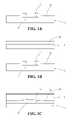
- FIGS. 1A to 1Hshow the various steps of a method of forming a metallic bump on an I/O pad according to an embodiment of the present invention.
- FIGS. 1A to 1Hshow the various steps of a method of forming a metallic bump on an I/O pad according to an embodiment of the present invention.
- an I/O pad 12is located on a side of a semiconductor device 10 which can be an integrated circuit (IC), a transistor, a diode, or a thyristor. For ease of reference, this side is referred to as the top side of the semiconductor device 10 .
- ICintegrated circuit
- a transistora transistor
- diodea diode
- a thyristora side of the semiconductor device 10
- an optional passivation layer 14which exposes part of the top surface of the I/O pad 12 .
- an UBM 16is formed to entirely cover the exposed top surface of the I/O pad 12 and part of the passivation layer 14 that is also on the top side of the I/O pad 12 .
- the formation of the UBM 16 and the passivation layer 14is conducted using any appropriate prior art technique. This should be well known to a skilled artisan in the related art and the details are therefore omitted here.
- an isolative layer 18 and a metallic foil 20are provided as shown in FIG. 1B .
- the isolative layer 18 and the metallic foil 20are arranged sequentially in this order on the top side of the structure of FIG. 1A and the result is shown in FIG. 1C .
- the material for the isolative layer 18is one such that the isolative layer 18 is in a liquid state or in a temporarily solid state within a specific temperature range. Then, by applying appropriate heat and pressure through the metallic foil 20 to the isolative layer 18 in the liquid state or in the temporarily solid state, the isolative layer 18 is permanently solidified and thereby tightly joined to the structure of FIG. 1A . If an isolative material with temporarily solid state is chosen, the isolative material should be able to turn into liquid state again within a certain temperature range while temperature is rising but before the permanently solidified state is reached. Alternatively, the metallic foil 20 can be attached to the isolative layer 18 first and, the combination is then attached to the top side of the structure of FIG. 1A .
- the metallic foil 20can be a copper foil, an aluminum foil, or a tin foil.
- the part of the metallic foil 20 directly covering the UBM 16is removed by laser ablation or chemical etching first and then the isolative layer 18 on the top side of the UBM 16 is removed by laser ablation or lithographic means. As such, the via 22 is formed and the UBM 16 is thereby exposed, as shown in FIG. 1D .
- a thin metallic layer 24 using electroless copper or nickelis formed at least in the via 22 using electroless deposition or sputtering, as shown in FIG. 1E .
- an additional metallic layercould be further formed by electroplating on the external surface of the thin metallic layer 24 .
- a resist 26is formed on a top side of the metallic foil 20 , without covering the via 22 coated with the thin metallic layer 24 .
- the metallic foil 20 and the thin metallic layer 24can jointly function as an electrode to conduct electrical current to form a metallic bump 28 in the via 22 on the top side of the UBM 16 using electroplating, as shown in FIG. 1G .
- the metallic bump 28can be either a solid one or a hollow one; and the metallic bump 28 can be formed to have a cylindrical body with a circular, rectangular, triangular, diamond-shaped, star-shaped, or polygonal cross section or with a cross section having two or more of the above shapes combined.
- the resist 26is removed and, by using laser or chemical etching, the metallic foil 20 is removed from both sides of the metallic bump 28 while a portion of the metallic foil 20 remains under the metallic bump 28 .
- Surface of copper bumpcan be coated with OSP (Organic Surface Protection), ENIG (Electroless Nickel Immersion Gold), Immersion Tin or Immersion Silver. The formation of the metallic bump 28 is therefore completed.
- the height of the metallic bump 28can be controlled by having the resist 26 to be of an appropriate height.
- the isolative layer 18 in the liquid stateis applied to the structure of FIG. 1A without the metallic foil 20
- the isolative layer 18can be solidified into the temporarily solid state first and the via 22 exposing the UBM 16 is formed using laser or lithographic means. Then, the metallic foil 20 is attached to the temporarily solidified isolative layer 18 and solidified permanently, and after part of metallic foil 20 on top of via 22 is removed by chemical etching or laser ablation the result is the same as what is shown in FIG. 1D .
- the same subsequent steps as described abovecan be conducted to form the metallic bump 28 .
- the isolative layer 18is applied to the structure of FIG. 1A and solidified. Then, the via 22 exposing the UBM 16 is formed using laser ablation or lithographic means. The thin metallic layer 24 is subsequently formed on the top side of the isolative layer 18 and in the via 22 by sputtering or electroless deposition. The thin metallic layer 24 is then thickened to achieve better conductivity by electroplating and the result would be similar to what is shown in FIG. 1E . The same subsequent steps as described above can be conducted to form the metallic bump 28 .
- the location of the UBM 16has to be determined first.
- fiducial markscan be prepared in advance on the bottom side of the semiconductor device 10 . Then, by inspecting the positions of the fiducial marks and their positional relationship to the I/O pad 12 , the exact location of the UBM 16 can be determined.
- An alternative approachis to utilize an X-ray apparatus that can “see” through the metallic foil 20 of FIG. 1C to directly determine the exact location of the UBM 16 .
- the most significant features of the present inventionare as follows. First, instead of only gold and solder, an element selected from a large collection of highly conductive metallic materials such as gold, silver, copper, tin, etc. or an alloy of these highly conductive metallic materials can be used to form the metallic bump 28 through electroless deposition and electroplating. Secondly, the metallic bump 28 's bonding to the I/O pad 12 is not solely relied on the adhesion between the metallic bump 28 and the UBM 16 . According to the present invention, the isolative layer 18 provides additional adhesion, thereby achieving a superior bonding between the metallic bump 28 and the I/O pad 12 .
Landscapes
- Engineering & Computer Science (AREA)
- Computer Hardware Design (AREA)
- Microelectronics & Electronic Packaging (AREA)
- Power Engineering (AREA)
- Physics & Mathematics (AREA)
- Condensed Matter Physics & Semiconductors (AREA)
- General Physics & Mathematics (AREA)
- Manufacturing & Machinery (AREA)
- Wire Bonding (AREA)
- Electroplating Methods And Accessories (AREA)
Abstract
Description
1. Field of the Invention
The present invention generally relates to chip packaging, and more particularly to a method of forming metallic bumps on the I/O pads of a semiconductor device
2. The Prior Arts
Flip-chip packaging utilizes bumps to establish electrical contact between a chip's I/O pads and the substrate (or lead frame) of the package. Structurally, a bump actually contains the bump itself and a so-called under bump metallurgy (UBM) located between the bump and an I/O pad.
An UBM generally contains an adhesion layer usually made of aluminum or chromium, a barrier layer usually made of copper, lead, or platinum, and a wetting layer usually made of gold, arranged in this order on the I/O pad. The bumps themselves, based on the material used, are classified as solder bumps and gold bumps.
To form solder bumps on the UBMs, usually either electroplating or printing method is used. For electroplating, patterned resists are first formed on the UBMs and then solders are plated. For printing, solders are first printed on the UBMs and the solders are thermally cured into the bumps. The two methods, however, all suffer disadvantages such as excessive bubbles, easy to peel off, etc and the production yield is therefore limited.
Electroplating similar to that used for solder bumps is also usually used to form gold bumps on UBMs so as to facilitate the subsequent Tape Carrier Package (TCP) or Chip On Glass (COG) process. Another method is to use a specialized wire bonding apparatus capable of melting gold wire into ball shape to perform bonding on the UBMs several times until the gold bumps reach a required height. Gold bumping, however, is not widely popular due to its high cost.
Therefore, a method of forming metallic bumps on I/O pads is provided herein. A major objective of the present invention is that the bumps can be formed using one or more materials selected from a large collection of highly conductive metallic materials. Another major objective of the present invention is to achieve enhanced bonding between the metallic bumps and the I/O pads, instead of relying on the UBMs alone.
To achieve the foregoing objectives, the method mainly contains the following steps. First, an UBM is formed on a top side of a semiconductor device's I/O pad. An isolative layer and a metallic foil are sequentially arranged in this order on the UBM. Then, a via is formed to expose the top surface of the UBM. Subsequently, a thin metallic layer is formed in the via and a resist is formed on the metallic foil. Then, by using the metallic foil and the thin metallic layer to conduct electrical current, a metallic bump is formed using electroplating in the via on the top side of the UBM. Finally, the resist and the metallic foil are removed and the formation of the metallic bump is completed.
The foregoing and other objects, features, aspects and advantages of the present invention will become better understood from a careful reading of a detailed description provided herein below with appropriate reference to the accompanying drawings.
The following descriptions are exemplary embodiments only, and are not intended to limit the scope, applicability or configuration of the invention in any way. Rather, the following description provides a convenient illustration for implementing exemplary embodiments of the invention. Various changes to the described embodiments may be made in the function and arrangement of the elements described without departing from the scope of the invention as set forth in the appended claims.
Then, according to the present embodiment, anisolative layer 18 and ametallic foil 20 are provided as shown inFIG. 1B . Theisolative layer 18 and themetallic foil 20 are arranged sequentially in this order on the top side of the structure ofFIG. 1A and the result is shown inFIG. 1C .
The material for theisolative layer 18 is one such that theisolative layer 18 is in a liquid state or in a temporarily solid state within a specific temperature range. Then, by applying appropriate heat and pressure through themetallic foil 20 to theisolative layer 18 in the liquid state or in the temporarily solid state, theisolative layer 18 is permanently solidified and thereby tightly joined to the structure ofFIG. 1A . If an isolative material with temporarily solid state is chosen, the isolative material should be able to turn into liquid state again within a certain temperature range while temperature is rising but before the permanently solidified state is reached. Alternatively, themetallic foil 20 can be attached to theisolative layer 18 first and, the combination is then attached to the top side of the structure ofFIG. 1A . Subsequently, by applying appropriate heat and pressure to theisolative layer 18, it is permanently solidified, thereby tightly joined to the structure ofFIG. 1A . Themetallic foil 20 can be a copper foil, an aluminum foil, or a tin foil.
Then, the part of themetallic foil 20 directly covering theUBM 16 is removed by laser ablation or chemical etching first and then theisolative layer 18 on the top side of theUBM 16 is removed by laser ablation or lithographic means. As such, thevia 22 is formed and the UBM16 is thereby exposed, as shown inFIG. 1D .
Subsequently, a thinmetallic layer 24 using electroless copper or nickel is formed at least in thevia 22 using electroless deposition or sputtering, as shown inFIG. 1E . For enhanced reliability, optionally an additional metallic layer could be further formed by electroplating on the external surface of the thinmetallic layer 24. Then, a resist26 is formed on a top side of themetallic foil 20, without covering the via22 coated with the thinmetallic layer 24. As such, themetallic foil 20 and the thinmetallic layer 24 can jointly function as an electrode to conduct electrical current to form ametallic bump 28 in the via22 on the top side of theUBM 16 using electroplating, as shown inFIG. 1G . Please note that, depending on the requirements of the subsequent packaging process, themetallic bump 28 can be either a solid one or a hollow one; and themetallic bump 28 can be formed to have a cylindrical body with a circular, rectangular, triangular, diamond-shaped, star-shaped, or polygonal cross section or with a cross section having two or more of the above shapes combined. Finally, as shown inFIG. 1H , the resist26 is removed and, by using laser or chemical etching, themetallic foil 20 is removed from both sides of themetallic bump 28 while a portion of themetallic foil 20 remains under themetallic bump 28. Surface of copper bump can be coated with OSP (Organic Surface Protection), ENIG (Electroless Nickel Immersion Gold), Immersion Tin or Immersion Silver. The formation of themetallic bump 28 is therefore completed. Please note that, the height of themetallic bump 28 can be controlled by having the resist26 to be of an appropriate height.
In an alternative embodiment where theisolative layer 18 in the liquid state is applied to the structure ofFIG. 1A without themetallic foil 20, theisolative layer 18 can be solidified into the temporarily solid state first and the via22 exposing theUBM 16 is formed using laser or lithographic means. Then, themetallic foil 20 is attached to the temporarily solidifiedisolative layer 18 and solidified permanently, and after part ofmetallic foil 20 on top of via22 is removed by chemical etching or laser ablation the result is the same as what is shown inFIG. 1D . The same subsequent steps as described above can be conducted to form themetallic bump 28.
In yet another alternative embodiment where themetallic foil 20 is not used at all, theisolative layer 18 is applied to the structure ofFIG. 1A and solidified. Then, the via22 exposing theUBM 16 is formed using laser ablation or lithographic means. The thinmetallic layer 24 is subsequently formed on the top side of theisolative layer 18 and in the via22 by sputtering or electroless deposition. The thinmetallic layer 24 is then thickened to achieve better conductivity by electroplating and the result would be similar to what is shown inFIG. 1E . The same subsequent steps as described above can be conducted to form themetallic bump 28.
To form the via22 so that it exposes theUBM 16 precisely, the location of theUBM 16 has to be determined first. To achieve that, fiducial marks can be prepared in advance on the bottom side of thesemiconductor device 10. Then, by inspecting the positions of the fiducial marks and their positional relationship to the I/O pad 12, the exact location of theUBM 16 can be determined. An alternative approach is to utilize an X-ray apparatus that can “see” through themetallic foil 20 ofFIG. 1C to directly determine the exact location of theUBM 16.
The most significant features of the present invention are as follows. First, instead of only gold and solder, an element selected from a large collection of highly conductive metallic materials such as gold, silver, copper, tin, etc. or an alloy of these highly conductive metallic materials can be used to form themetallic bump 28 through electroless deposition and electroplating. Secondly, themetallic bump 28's bonding to the I/O pad 12 is not solely relied on the adhesion between themetallic bump 28 and theUBM 16. According to the present invention, theisolative layer 18 provides additional adhesion, thereby achieving a superior bonding between themetallic bump 28 and the I/O pad 12.
Although the present invention has been described with reference to the preferred embodiments, it will be understood that the invention is not limited to the details described thereof. Various substitutions and modifications have been suggested in the foregoing description, and others will occur to those of ordinary skill in the art. Therefore, all such substitutions and modifications are intended to be embraced within the scope of the invention as defined in the appended claims.
Claims (10)
1. A method of forming a metallic bump for establishing electrical contact to an I/O pad of a semiconductor device, comprising the steps of:
preparing said semiconductor device having at least said I/O pad for electrical connection;
forming an under bump metallurgy (UBM) on a top side of said I/O pad for electrical connection to said I/O pad;
forming an isolative layer and a metallic foil sequentially in this order on a top side of said semiconductor device to cover said UBM entirely;
forming a via by removing a part of said isolative layer and said metallic foil until a substantial part of said top side of said UBM is exposed;
forming a thin metallic layer at least in said via;
forming resist on a top side of said metallic foil without covering said via coated with said thin metallic layer;
forming said metallic bump in said via on said top side of said UBM by using said metallic foil and said thin metallic layer jointly to conduct electrical current; and
removing said resist and said metallic foil.
2. The method according toclaim 1 , wherein said semiconductor device is one of an integrated circuit, a transistor, a diode, and a thyristor.
3. The method according toclaim 1 , wherein said UBM comprises an adhesion layer, a barrier layer, and a wetting layer.
4. The method according toclaim 1 , wherein said metallic foil is one of a copper foil, an aluminum foil, and a tin foil.
5. The method according toclaim 1 , wherein said thin metallic layer is made of one of electroless copper and nickel.
6. The method according toclaim 1 , wherein said metallic bump is made of one of the elements gold, silver, copper, tin, and an alloy of said elements.
7. The method according toclaim 1 , wherein said bump is one of a solid bump and a hollow bump.
8. The method according toclaim 1 , wherein said metallic bump has a cylindrical shape having one of a circular, rectangular, triangular, diamond-shaped, star-shaped, and polygonal cross section.
9. The method according toclaim 1 , further comprising the step of:
forming an additional metallic layer by electroplating on the external surface of said thin metallic layer before forming said resist.
10. The method according toclaim 3 , wherein said adhesion layer is made of one of aluminum and chromium; said barrier layer is made of one of copper, lead, and platinum; and said wetting layer is made of gold.
Priority Applications (2)
| Application Number | Priority Date | Filing Date | Title |
|---|---|---|---|
| US11/871,974US7713860B2 (en) | 2007-10-13 | 2007-10-13 | Method of forming metallic bump on I/O pad |
| US12/016,209US7713861B2 (en) | 2007-10-13 | 2008-01-18 | Method of forming metallic bump and seal for semiconductor device |
Applications Claiming Priority (1)
| Application Number | Priority Date | Filing Date | Title |
|---|---|---|---|
| US11/871,974US7713860B2 (en) | 2007-10-13 | 2007-10-13 | Method of forming metallic bump on I/O pad |
Related Child Applications (1)
| Application Number | Title | Priority Date | Filing Date |
|---|---|---|---|
| US12/016,209Continuation-In-PartUS7713861B2 (en) | 2007-10-13 | 2008-01-18 | Method of forming metallic bump and seal for semiconductor device |
Publications (2)
| Publication Number | Publication Date |
|---|---|
| US20090098723A1 US20090098723A1 (en) | 2009-04-16 |
| US7713860B2true US7713860B2 (en) | 2010-05-11 |
Family
ID=40534656
Family Applications (1)
| Application Number | Title | Priority Date | Filing Date |
|---|---|---|---|
| US11/871,974Expired - Fee RelatedUS7713860B2 (en) | 2007-10-13 | 2007-10-13 | Method of forming metallic bump on I/O pad |
Country Status (1)
| Country | Link |
|---|---|
| US (1) | US7713860B2 (en) |
Cited By (10)
| Publication number | Priority date | Publication date | Assignee | Title |
|---|---|---|---|---|
| US20100084763A1 (en)* | 2008-10-06 | 2010-04-08 | Wan-Ling Yu | Metallic Bump Structure Without Under Bump Metallurgy And Manufacturing Method Thereof |
| US20110057307A1 (en)* | 2009-09-10 | 2011-03-10 | Topacio Roden R | Semiconductor Chip with Stair Arrangement Bump Structures |
| CN102931099A (en)* | 2012-11-08 | 2013-02-13 | 南通富士通微电子股份有限公司 | Method for forming semiconductor component |
| US8816499B2 (en) | 2012-05-24 | 2014-08-26 | Samsung Electronics Co., Ltd. | Electrical interconnections of semiconductor devices and methods for fabricating the same |
| CN105023906A (en)* | 2014-04-16 | 2015-11-04 | 矽品精密工业股份有限公司 | Substrate with electrical connection structure and manufacturing method thereof |
| US9293432B2 (en) | 2012-11-08 | 2016-03-22 | Nantong Fujitsu Microelectronics Co., Ltd. | Metal contact for chip packaging structure |
| US9379077B2 (en) | 2012-11-08 | 2016-06-28 | Nantong Fujitsu Microelectronics Co., Ltd. | Metal contact for semiconductor device |
| US9548282B2 (en) | 2012-11-08 | 2017-01-17 | Nantong Fujitsu Microelectronics Co., Ltd. | Metal contact for semiconductor device |
| US20170084558A1 (en)* | 2015-09-18 | 2017-03-23 | Samsung Electronics Co., Ltd. | Semiconductor package |
| US20220068861A1 (en)* | 2011-12-15 | 2022-03-03 | Intel Corporation | Packaged semiconductor die with bumpless die-package interface for bumpless build-up layer (bbul) packages |
Families Citing this family (10)
| Publication number | Priority date | Publication date | Assignee | Title |
|---|---|---|---|---|
| US7994045B1 (en)* | 2009-09-08 | 2011-08-09 | Amkor Technology, Inc. | Bumped chip package fabrication method and structure |
| KR20110090344A (en)* | 2010-02-03 | 2011-08-10 | 삼성전자주식회사 | Bonding structure manufacturing apparatus, bonding structure and method of forming the same |
| US10833033B2 (en) | 2011-07-27 | 2020-11-10 | Taiwan Semiconductor Manufacturing Co., Ltd. | Bump structure having a side recess and semiconductor structure including the same |
| CN102931109B (en)* | 2012-11-08 | 2015-06-03 | 南通富士通微电子股份有限公司 | Method for forming semiconductor devices |
| US9761549B2 (en) | 2012-11-08 | 2017-09-12 | Tongfu Microelectronics Co., Ltd. | Semiconductor device and fabrication method |
| CN102915982B (en)* | 2012-11-08 | 2015-03-11 | 南通富士通微电子股份有限公司 | Semiconductor device |
| US9295163B2 (en)* | 2013-05-30 | 2016-03-22 | Dyi-chung Hu | Method of making a circuit board structure with embedded fine-pitch wires |
| DE102017122454A1 (en)* | 2017-09-27 | 2019-01-17 | Infineon Technologies Ag | Flexible crown-shaped bump for flip-chip mounting |
| WO2020103708A1 (en)* | 2018-11-20 | 2020-05-28 | Changxin Memory Technologies, Inc. | Copper pillar bump structure and fabricating method thereof |
| CN119852281B (en)* | 2025-03-19 | 2025-09-23 | 深圳市联合蓝海应用材料科技股份有限公司 | A semiconductor device structure and its manufacturing method and chip |
Citations (52)
| Publication number | Priority date | Publication date | Assignee | Title |
|---|---|---|---|---|
| US4742023A (en)* | 1986-08-28 | 1988-05-03 | Fujitsu Limited | Method for producing a semiconductor device |
| US5293006A (en)* | 1991-09-13 | 1994-03-08 | Mcnc | Solder bump including circular lip |
| US5418186A (en)* | 1993-07-15 | 1995-05-23 | Samsung Electronics Co., Ltd. | Method for manufacturing a bump on a semiconductor chip |
| US5445979A (en)* | 1993-12-28 | 1995-08-29 | Fujitsu Limited | Method of making field effect compound semiconductor device with eaves electrode |
| US5492235A (en)* | 1995-12-18 | 1996-02-20 | Intel Corporation | Process for single mask C4 solder bump fabrication |
| US5508229A (en)* | 1994-05-24 | 1996-04-16 | National Semiconductor Corporation | Method for forming solder bumps in semiconductor devices |
| US5888892A (en)* | 1995-05-24 | 1999-03-30 | Sony Corporation | Metal layer pattern forming method |
| US5895271A (en)* | 1994-12-29 | 1999-04-20 | Sony Corporation | Metal film forming method |
| US5933752A (en)* | 1996-11-28 | 1999-08-03 | Sony Corporation | Method and apparatus for forming solder bumps for a semiconductor device |
| US5946590A (en)* | 1996-12-10 | 1999-08-31 | Citizen Watch Co., Ltd. | Method for making bumps |
| US6117299A (en)* | 1997-05-09 | 2000-09-12 | Mcnc | Methods of electroplating solder bumps of uniform height on integrated circuit substrates |
| US6162652A (en)* | 1997-12-31 | 2000-12-19 | Intel Corporation | Process for sort testing C4 bumped wafers |
| US6169021B1 (en)* | 1998-07-06 | 2001-01-02 | Micron Technology, Inc. | Method of making a metallized recess in a substrate |
| US6268114B1 (en)* | 1998-09-18 | 2001-07-31 | Taiwan Semiconductor Manufacturing Company, Ltd | Method for forming fine-pitched solder bumps |
| US20020003160A1 (en)* | 1998-03-26 | 2002-01-10 | Masud Beroz | Components with conductive solder mask layers |
| US20020020551A1 (en)* | 1995-04-04 | 2002-02-21 | Mcnc | Controlled-shaped solder reservoirs for increasing the volume of solder bumps |
| US6372545B1 (en)* | 2001-03-22 | 2002-04-16 | Taiwan Semiconductor Manufacturing Company | Method for under bump metal patterning of bumping process |
| US6413851B1 (en)* | 2001-06-12 | 2002-07-02 | Advanced Interconnect Technology, Ltd. | Method of fabrication of barrier cap for under bump metal |
| US6426556B1 (en)* | 2001-01-16 | 2002-07-30 | Megic Corporation | Reliable metal bumps on top of I/O pads with test probe marks |
| US6555908B1 (en)* | 2000-02-10 | 2003-04-29 | Epic Technologies, Inc. | Compliant, solderable input/output bump structures |
| US6586322B1 (en)* | 2001-12-21 | 2003-07-01 | Taiwan Semiconductor Manufacturing Co., Ltd. | Method of making a bump on a substrate using multiple photoresist layers |
| US6649533B1 (en)* | 1999-05-05 | 2003-11-18 | Advanced Micro Devices, Inc. | Method and apparatus for forming an under bump metallurgy layer |
| US20030216039A1 (en)* | 2002-05-17 | 2003-11-20 | Taiwan Semiconductor Manufacturing Company | Method for fabricating an under bump metallization structure |
| US6667230B2 (en)* | 2001-07-12 | 2003-12-23 | Taiwan Semiconductor Manufacturing Co., Ltd. | Passivation and planarization process for flip chip packages |
| US6696356B2 (en)* | 2001-12-31 | 2004-02-24 | Taiwan Semiconductor Manufacturing Co., Ltd. | Method of making a bump on a substrate without ribbon residue |
| US20040115934A1 (en)* | 2002-12-13 | 2004-06-17 | Jerry Broz | Method of improving contact resistance |
| US20040182915A1 (en)* | 2002-12-20 | 2004-09-23 | Bachman Mark Adam | Structure and method for bonding to copper interconnect structures |
| US6815324B2 (en)* | 2001-02-15 | 2004-11-09 | Megic Corporation | Reliable metal bumps on top of I/O pads after removal of test probe marks |
| US20040247840A1 (en)* | 2003-01-30 | 2004-12-09 | Yoshihiro Sugiura | Electronic elements, method for manufacturing electronic elements, circuit substrates, method for manufacturing circuit substrates, electronic devices and method for manufacturing electronic devices |
| US6849534B2 (en)* | 2002-10-25 | 2005-02-01 | Via Technologies, Inc. | Process of forming bonding columns |
| US20050042872A1 (en)* | 2003-08-21 | 2005-02-24 | Siliconware Precision Industries Co., Ltd., Taiwan, R.O.C. | Process for forming lead-free bump on electronic component |
| US6878633B2 (en)* | 2002-12-23 | 2005-04-12 | Freescale Semiconductor, Inc. | Flip-chip structure and method for high quality inductors and transformers |
| US20050116340A1 (en)* | 2003-10-09 | 2005-06-02 | Seiko Epson Corporation | Semiconductor device and method of manufacturing the same |
| US20050164483A1 (en)* | 2003-08-21 | 2005-07-28 | Jeong Se-Young | Method of forming solder bump with reduced surface defects |
| US20050242436A1 (en)* | 2004-04-14 | 2005-11-03 | Hideaki Abe | Display device and manufacturing method of the same |
| US20050258539A1 (en)* | 2004-05-20 | 2005-11-24 | Nec Electronics Corporation | Semiconductor device |
| US20050272242A1 (en)* | 2003-07-18 | 2005-12-08 | Tsung-Yen Tseng | Formation method for conductive bump |
| US7007834B2 (en)* | 2000-12-20 | 2006-03-07 | PAC Tech—Packaging Technologies GmbH | Contact bump construction for the production of a connector construction for substrate connecting surfaces |
| US20060051954A1 (en)* | 2004-09-07 | 2006-03-09 | Siliconware Precision Industries Co, Ltd. | Bump structure of semiconductor package and method for fabricating the same |
| US20060134884A1 (en)* | 2004-11-30 | 2006-06-22 | Advanced Semiconductor Engineering, Inc. | Wafer structure, chip structure, and fabricating process thereof |
| US20060170102A1 (en)* | 2005-01-28 | 2006-08-03 | Samsung Electronics Co., Ltd. | Bump structure of semiconductor device and method of manufacturing the same |
| US20070087544A1 (en)* | 2005-10-19 | 2007-04-19 | Taiwan Semiconductor Manufacturing Co., Ltd. | Method for forming improved bump structure |
| US20070130763A1 (en)* | 2004-04-12 | 2007-06-14 | Phoenix Precision Technology Corporation | Method of fabricating electrical connection terminal of embedded chip |
| US20070155155A1 (en)* | 2003-03-10 | 2007-07-05 | Kazumasa Tanida | Manufacturing method for semiconductor device and semiconductor device |
| US7250362B2 (en)* | 2003-09-09 | 2007-07-31 | Advanced Semiconductor Engineering Inc. | Solder bump structure and method for forming the same |
| US20070182007A1 (en)* | 2006-02-06 | 2007-08-09 | Taiwan Semiconductor Manufacturing Co., Ltd. | Solder bump on a semiconductor substrate |
| US20070182004A1 (en)* | 2006-02-08 | 2007-08-09 | Rinne Glenn A | Methods of Forming Electronic Interconnections Including Compliant Dielectric Layers and Related Devices |
| US20070290343A1 (en)* | 2006-06-15 | 2007-12-20 | Sony Corporation | Electronic component, semiconductor device employing same, and method for manufacturing electronic component |
| US20080050905A1 (en)* | 2006-05-29 | 2008-02-28 | Kabushiki Kaisha Toshiba | Method of manufacturing semiconductor device |
| US20080169559A1 (en)* | 2007-01-16 | 2008-07-17 | Chipmos Technologies (Bermuda) Ltd. | Bump structure with annular support and manufacturing method thereof |
| US20090057909A1 (en)* | 2007-06-20 | 2009-03-05 | Flipchip International, Llc | Under bump metallization structure having a seed layer for electroless nickel deposition |
| US20090096099A1 (en)* | 2007-10-16 | 2009-04-16 | Phoenix Precision Technology Corporation | Package substrate and method for fabricating the same |
- 2007
- 2007-10-13USUS11/871,974patent/US7713860B2/ennot_activeExpired - Fee Related
Patent Citations (57)
| Publication number | Priority date | Publication date | Assignee | Title |
|---|---|---|---|---|
| US4742023A (en)* | 1986-08-28 | 1988-05-03 | Fujitsu Limited | Method for producing a semiconductor device |
| US5293006A (en)* | 1991-09-13 | 1994-03-08 | Mcnc | Solder bump including circular lip |
| US5418186A (en)* | 1993-07-15 | 1995-05-23 | Samsung Electronics Co., Ltd. | Method for manufacturing a bump on a semiconductor chip |
| US5445979A (en)* | 1993-12-28 | 1995-08-29 | Fujitsu Limited | Method of making field effect compound semiconductor device with eaves electrode |
| US5508229A (en)* | 1994-05-24 | 1996-04-16 | National Semiconductor Corporation | Method for forming solder bumps in semiconductor devices |
| US5895271A (en)* | 1994-12-29 | 1999-04-20 | Sony Corporation | Metal film forming method |
| US20020020551A1 (en)* | 1995-04-04 | 2002-02-21 | Mcnc | Controlled-shaped solder reservoirs for increasing the volume of solder bumps |
| US5888892A (en)* | 1995-05-24 | 1999-03-30 | Sony Corporation | Metal layer pattern forming method |
| US5492235A (en)* | 1995-12-18 | 1996-02-20 | Intel Corporation | Process for single mask C4 solder bump fabrication |
| US5933752A (en)* | 1996-11-28 | 1999-08-03 | Sony Corporation | Method and apparatus for forming solder bumps for a semiconductor device |
| US5946590A (en)* | 1996-12-10 | 1999-08-31 | Citizen Watch Co., Ltd. | Method for making bumps |
| US6117299A (en)* | 1997-05-09 | 2000-09-12 | Mcnc | Methods of electroplating solder bumps of uniform height on integrated circuit substrates |
| US6162652A (en)* | 1997-12-31 | 2000-12-19 | Intel Corporation | Process for sort testing C4 bumped wafers |
| US20020003160A1 (en)* | 1998-03-26 | 2002-01-10 | Masud Beroz | Components with conductive solder mask layers |
| US6169021B1 (en)* | 1998-07-06 | 2001-01-02 | Micron Technology, Inc. | Method of making a metallized recess in a substrate |
| US6268114B1 (en)* | 1998-09-18 | 2001-07-31 | Taiwan Semiconductor Manufacturing Company, Ltd | Method for forming fine-pitched solder bumps |
| US6649533B1 (en)* | 1999-05-05 | 2003-11-18 | Advanced Micro Devices, Inc. | Method and apparatus for forming an under bump metallurgy layer |
| US6555908B1 (en)* | 2000-02-10 | 2003-04-29 | Epic Technologies, Inc. | Compliant, solderable input/output bump structures |
| US7007834B2 (en)* | 2000-12-20 | 2006-03-07 | PAC Tech—Packaging Technologies GmbH | Contact bump construction for the production of a connector construction for substrate connecting surfaces |
| US6426556B1 (en)* | 2001-01-16 | 2002-07-30 | Megic Corporation | Reliable metal bumps on top of I/O pads with test probe marks |
| US20020105076A1 (en)* | 2001-01-16 | 2002-08-08 | Megic Corporation | Reliable metal bumps on top of i/o pads with test probe marks |
| US6815324B2 (en)* | 2001-02-15 | 2004-11-09 | Megic Corporation | Reliable metal bumps on top of I/O pads after removal of test probe marks |
| US6372545B1 (en)* | 2001-03-22 | 2002-04-16 | Taiwan Semiconductor Manufacturing Company | Method for under bump metal patterning of bumping process |
| US6413851B1 (en)* | 2001-06-12 | 2002-07-02 | Advanced Interconnect Technology, Ltd. | Method of fabrication of barrier cap for under bump metal |
| US6667230B2 (en)* | 2001-07-12 | 2003-12-23 | Taiwan Semiconductor Manufacturing Co., Ltd. | Passivation and planarization process for flip chip packages |
| US6586322B1 (en)* | 2001-12-21 | 2003-07-01 | Taiwan Semiconductor Manufacturing Co., Ltd. | Method of making a bump on a substrate using multiple photoresist layers |
| US6696356B2 (en)* | 2001-12-31 | 2004-02-24 | Taiwan Semiconductor Manufacturing Co., Ltd. | Method of making a bump on a substrate without ribbon residue |
| US20030216039A1 (en)* | 2002-05-17 | 2003-11-20 | Taiwan Semiconductor Manufacturing Company | Method for fabricating an under bump metallization structure |
| US6849534B2 (en)* | 2002-10-25 | 2005-02-01 | Via Technologies, Inc. | Process of forming bonding columns |
| US20040115934A1 (en)* | 2002-12-13 | 2004-06-17 | Jerry Broz | Method of improving contact resistance |
| US20040182915A1 (en)* | 2002-12-20 | 2004-09-23 | Bachman Mark Adam | Structure and method for bonding to copper interconnect structures |
| US6878633B2 (en)* | 2002-12-23 | 2005-04-12 | Freescale Semiconductor, Inc. | Flip-chip structure and method for high quality inductors and transformers |
| US20040247840A1 (en)* | 2003-01-30 | 2004-12-09 | Yoshihiro Sugiura | Electronic elements, method for manufacturing electronic elements, circuit substrates, method for manufacturing circuit substrates, electronic devices and method for manufacturing electronic devices |
| US20070155155A1 (en)* | 2003-03-10 | 2007-07-05 | Kazumasa Tanida | Manufacturing method for semiconductor device and semiconductor device |
| US20050272242A1 (en)* | 2003-07-18 | 2005-12-08 | Tsung-Yen Tseng | Formation method for conductive bump |
| US7132358B2 (en)* | 2003-08-21 | 2006-11-07 | Samsung Electronics Co., Ltd. | Method of forming solder bump with reduced surface defects |
| US20050164483A1 (en)* | 2003-08-21 | 2005-07-28 | Jeong Se-Young | Method of forming solder bump with reduced surface defects |
| US20050042872A1 (en)* | 2003-08-21 | 2005-02-24 | Siliconware Precision Industries Co., Ltd., Taiwan, R.O.C. | Process for forming lead-free bump on electronic component |
| US7250362B2 (en)* | 2003-09-09 | 2007-07-31 | Advanced Semiconductor Engineering Inc. | Solder bump structure and method for forming the same |
| US20050116340A1 (en)* | 2003-10-09 | 2005-06-02 | Seiko Epson Corporation | Semiconductor device and method of manufacturing the same |
| US20060237842A1 (en)* | 2003-10-09 | 2006-10-26 | Seiko Epson Corporation | Semiconductor device including an under electrode and a bump electrode |
| US20070130763A1 (en)* | 2004-04-12 | 2007-06-14 | Phoenix Precision Technology Corporation | Method of fabricating electrical connection terminal of embedded chip |
| US20050242436A1 (en)* | 2004-04-14 | 2005-11-03 | Hideaki Abe | Display device and manufacturing method of the same |
| US20070063346A1 (en)* | 2004-04-14 | 2007-03-22 | Hideaki Abe | Display device and manufacturing method of the same |
| US20050258539A1 (en)* | 2004-05-20 | 2005-11-24 | Nec Electronics Corporation | Semiconductor device |
| US20060051954A1 (en)* | 2004-09-07 | 2006-03-09 | Siliconware Precision Industries Co, Ltd. | Bump structure of semiconductor package and method for fabricating the same |
| US20060134884A1 (en)* | 2004-11-30 | 2006-06-22 | Advanced Semiconductor Engineering, Inc. | Wafer structure, chip structure, and fabricating process thereof |
| US20060170102A1 (en)* | 2005-01-28 | 2006-08-03 | Samsung Electronics Co., Ltd. | Bump structure of semiconductor device and method of manufacturing the same |
| US20070087544A1 (en)* | 2005-10-19 | 2007-04-19 | Taiwan Semiconductor Manufacturing Co., Ltd. | Method for forming improved bump structure |
| US20070182007A1 (en)* | 2006-02-06 | 2007-08-09 | Taiwan Semiconductor Manufacturing Co., Ltd. | Solder bump on a semiconductor substrate |
| US7449785B2 (en)* | 2006-02-06 | 2008-11-11 | Taiwan Semiconductor Manufacturing Co., Ltd. | Solder bump on a semiconductor substrate |
| US20070182004A1 (en)* | 2006-02-08 | 2007-08-09 | Rinne Glenn A | Methods of Forming Electronic Interconnections Including Compliant Dielectric Layers and Related Devices |
| US20080050905A1 (en)* | 2006-05-29 | 2008-02-28 | Kabushiki Kaisha Toshiba | Method of manufacturing semiconductor device |
| US20070290343A1 (en)* | 2006-06-15 | 2007-12-20 | Sony Corporation | Electronic component, semiconductor device employing same, and method for manufacturing electronic component |
| US20080169559A1 (en)* | 2007-01-16 | 2008-07-17 | Chipmos Technologies (Bermuda) Ltd. | Bump structure with annular support and manufacturing method thereof |
| US20090057909A1 (en)* | 2007-06-20 | 2009-03-05 | Flipchip International, Llc | Under bump metallization structure having a seed layer for electroless nickel deposition |
| US20090096099A1 (en)* | 2007-10-16 | 2009-04-16 | Phoenix Precision Technology Corporation | Package substrate and method for fabricating the same |
Cited By (14)
| Publication number | Priority date | Publication date | Assignee | Title |
|---|---|---|---|---|
| US20100084763A1 (en)* | 2008-10-06 | 2010-04-08 | Wan-Ling Yu | Metallic Bump Structure Without Under Bump Metallurgy And Manufacturing Method Thereof |
| US7968446B2 (en)* | 2008-10-06 | 2011-06-28 | Wan-Ling Yu | Metallic bump structure without under bump metallurgy and manufacturing method thereof |
| US20110057307A1 (en)* | 2009-09-10 | 2011-03-10 | Topacio Roden R | Semiconductor Chip with Stair Arrangement Bump Structures |
| US20220068861A1 (en)* | 2011-12-15 | 2022-03-03 | Intel Corporation | Packaged semiconductor die with bumpless die-package interface for bumpless build-up layer (bbul) packages |
| US8816499B2 (en) | 2012-05-24 | 2014-08-26 | Samsung Electronics Co., Ltd. | Electrical interconnections of semiconductor devices and methods for fabricating the same |
| US9293432B2 (en) | 2012-11-08 | 2016-03-22 | Nantong Fujitsu Microelectronics Co., Ltd. | Metal contact for chip packaging structure |
| CN102931099B (en)* | 2012-11-08 | 2016-05-18 | 南通富士通微电子股份有限公司 | The formation method of semiconductor devices |
| US9379077B2 (en) | 2012-11-08 | 2016-06-28 | Nantong Fujitsu Microelectronics Co., Ltd. | Metal contact for semiconductor device |
| US9548282B2 (en) | 2012-11-08 | 2017-01-17 | Nantong Fujitsu Microelectronics Co., Ltd. | Metal contact for semiconductor device |
| CN102931099A (en)* | 2012-11-08 | 2013-02-13 | 南通富士通微电子股份有限公司 | Method for forming semiconductor component |
| CN105023906A (en)* | 2014-04-16 | 2015-11-04 | 矽品精密工业股份有限公司 | Substrate with electrical connection structure and manufacturing method thereof |
| CN105023906B (en)* | 2014-04-16 | 2018-10-09 | 矽品精密工业股份有限公司 | Substrate with electrical connection structure and manufacturing method thereof |
| US20170084558A1 (en)* | 2015-09-18 | 2017-03-23 | Samsung Electronics Co., Ltd. | Semiconductor package |
| US10008462B2 (en)* | 2015-09-18 | 2018-06-26 | Samsung Electronics Co., Ltd. | Semiconductor package |
Also Published As
| Publication number | Publication date |
|---|---|
| US20090098723A1 (en) | 2009-04-16 |
Similar Documents
| Publication | Publication Date | Title |
|---|---|---|
| US7713860B2 (en) | Method of forming metallic bump on I/O pad | |
| US7713861B2 (en) | Method of forming metallic bump and seal for semiconductor device | |
| US7968446B2 (en) | Metallic bump structure without under bump metallurgy and manufacturing method thereof | |
| KR100514230B1 (en) | Method for forming bump and method for making semiconductor device | |
| JP3262497B2 (en) | Chip mounted circuit card structure | |
| JP3320979B2 (en) | How to mount a device directly on a device carrier | |
| TWI431701B (en) | Fusible I/O interconnection system and flip chip packaging method involving columnar bumps for substrate mounting | |
| US6787903B2 (en) | Semiconductor device with under bump metallurgy and method for fabricating the same | |
| US10600709B2 (en) | Bump-on-trace packaging structure and method for forming the same | |
| US8022530B2 (en) | Package substrate having electrically connecting structure | |
| US20090289360A1 (en) | Workpiece contact pads with elevated ring for restricting horizontal movement of terminals of ic during pressing | |
| KR101034161B1 (en) | Semiconductor package substrate | |
| US7956472B2 (en) | Packaging substrate having electrical connection structure and method for fabricating the same | |
| TWI502666B (en) | Electronic parts mounting body, electronic parts, substrate | |
| US6905915B2 (en) | Semiconductor device and method of manufacturing the same, and electronic instrument | |
| US7078272B2 (en) | Wafer scale integration packaging and method of making and using the same | |
| KR101115705B1 (en) | Method of forming metallic bump and seal for semiconductor device | |
| KR20100080352A (en) | Semiconductor package substrate with metal bumps | |
| US8174113B2 (en) | Methods of fabricating robust integrated heat spreader designs and structures formed thereby | |
| US20120126397A1 (en) | Semiconductor substrate and method thereof | |
| KR101050567B1 (en) | Metal bump formation method on semiconductor connection pad | |
| KR20100048622A (en) | A metallic bump structure without under bump metallurgy and a manufacturing method thereof | |
| US20050275097A1 (en) | Method of forming a solder bump and the structure thereof | |
| JP2008098210A (en) | Protruding electrode forming method, semiconductor device manufacturing method, and semiconductor device | |
| JP5436836B2 (en) | Manufacturing method of semiconductor device embedded substrate |
Legal Events
| Date | Code | Title | Description |
|---|---|---|---|
| FPAY | Fee payment | Year of fee payment:4 | |
| FEPP | Fee payment procedure | Free format text:MAINTENANCE FEE REMINDER MAILED (ORIGINAL EVENT CODE: REM.) | |
| LAPS | Lapse for failure to pay maintenance fees | Free format text:PATENT EXPIRED FOR FAILURE TO PAY MAINTENANCE FEES (ORIGINAL EVENT CODE: EXP.) | |
| STCH | Information on status: patent discontinuation | Free format text:PATENT EXPIRED DUE TO NONPAYMENT OF MAINTENANCE FEES UNDER 37 CFR 1.362 | |
| FP | Lapsed due to failure to pay maintenance fee | Effective date:20180511 |