US7713841B2 - Methods for thinning semiconductor substrates that employ support structures formed on the substrates - Google Patents
Methods for thinning semiconductor substrates that employ support structures formed on the substratesDownload PDFInfo
- Publication number
- US7713841B2 US7713841B2US10/666,742US66674203AUS7713841B2US 7713841 B2US7713841 B2US 7713841B2US 66674203 AUS66674203 AUS 66674203AUS 7713841 B2US7713841 B2US 7713841B2
- Authority
- US
- United States
- Prior art keywords
- semiconductor substrate
- support structure
- active surface
- support
- outer peripheral
- Prior art date
- Legal status (The legal status is an assumption and is not a legal conclusion. Google has not performed a legal analysis and makes no representation as to the accuracy of the status listed.)
- Expired - Lifetime
Links
Images


Classifications
- G—PHYSICS
- G03—PHOTOGRAPHY; CINEMATOGRAPHY; ANALOGOUS TECHNIQUES USING WAVES OTHER THAN OPTICAL WAVES; ELECTROGRAPHY; HOLOGRAPHY
- G03F—PHOTOMECHANICAL PRODUCTION OF TEXTURED OR PATTERNED SURFACES, e.g. FOR PRINTING, FOR PROCESSING OF SEMICONDUCTOR DEVICES; MATERIALS THEREFOR; ORIGINALS THEREFOR; APPARATUS SPECIALLY ADAPTED THEREFOR
- G03F7/00—Photomechanical, e.g. photolithographic, production of textured or patterned surfaces, e.g. printing surfaces; Materials therefor, e.g. comprising photoresists; Apparatus specially adapted therefor
- G03F7/0037—Production of three-dimensional images
- B—PERFORMING OPERATIONS; TRANSPORTING
- B33—ADDITIVE MANUFACTURING TECHNOLOGY
- B33Y—ADDITIVE MANUFACTURING, i.e. MANUFACTURING OF THREE-DIMENSIONAL [3-D] OBJECTS BY ADDITIVE DEPOSITION, ADDITIVE AGGLOMERATION OR ADDITIVE LAYERING, e.g. BY 3-D PRINTING, STEREOLITHOGRAPHY OR SELECTIVE LASER SINTERING
- B33Y30/00—Apparatus for additive manufacturing; Details thereof or accessories therefor
- B—PERFORMING OPERATIONS; TRANSPORTING
- B33—ADDITIVE MANUFACTURING TECHNOLOGY
- B33Y—ADDITIVE MANUFACTURING, i.e. MANUFACTURING OF THREE-DIMENSIONAL [3-D] OBJECTS BY ADDITIVE DEPOSITION, ADDITIVE AGGLOMERATION OR ADDITIVE LAYERING, e.g. BY 3-D PRINTING, STEREOLITHOGRAPHY OR SELECTIVE LASER SINTERING
- B33Y70/00—Materials specially adapted for additive manufacturing
- B33Y70/10—Composites of different types of material, e.g. mixtures of ceramics and polymers or mixtures of metals and biomaterials
- B—PERFORMING OPERATIONS; TRANSPORTING
- B33—ADDITIVE MANUFACTURING TECHNOLOGY
- B33Y—ADDITIVE MANUFACTURING, i.e. MANUFACTURING OF THREE-DIMENSIONAL [3-D] OBJECTS BY ADDITIVE DEPOSITION, ADDITIVE AGGLOMERATION OR ADDITIVE LAYERING, e.g. BY 3-D PRINTING, STEREOLITHOGRAPHY OR SELECTIVE LASER SINTERING
- B33Y80/00—Products made by additive manufacturing
- G—PHYSICS
- G03—PHOTOGRAPHY; CINEMATOGRAPHY; ANALOGOUS TECHNIQUES USING WAVES OTHER THAN OPTICAL WAVES; ELECTROGRAPHY; HOLOGRAPHY
- G03F—PHOTOMECHANICAL PRODUCTION OF TEXTURED OR PATTERNED SURFACES, e.g. FOR PRINTING, FOR PROCESSING OF SEMICONDUCTOR DEVICES; MATERIALS THEREFOR; ORIGINALS THEREFOR; APPARATUS SPECIALLY ADAPTED THEREFOR
- G03F7/00—Photomechanical, e.g. photolithographic, production of textured or patterned surfaces, e.g. printing surfaces; Materials therefor, e.g. comprising photoresists; Apparatus specially adapted therefor
- G03F7/004—Photosensitive materials
- G03F7/0047—Photosensitive materials characterised by additives for obtaining a metallic or ceramic pattern, e.g. by firing
Definitions
- the present inventionrelates to structures for supporting semiconductor substrates during and following thinning thereof. More specifically, the present invention relates to support structures that are configured to entirely cover at least the outer peripheral portions of the active surfaces of semiconductor substrates to impart the semiconductor substrates with some rigidity following thinning thereof.
- One of the approaches that has been taken for reducing the size of semiconductor device packages or for facilitating the incorporation of more semiconductor dice into packages of a standard sizehas been to reduce sizes of the various package features, including the wire bond heights, the thicknesses of adhesive layers, the thickness of packaging material which covers the package components, and the thicknesses of the semiconductor dice themselves.
- the thicknesses of semiconductor dicemay be reduced prior to singulation thereof from a semiconductor substrate, typically in the form of a silicon wafer, by reducing the thickness of the entire semiconductor substrate. This is typically done by so-called “backgrinding” processes, which include mechanical or chemical removal of material from the back side of the semiconductor substrate and, thus, from the devices, or dice, that have been fabricated on the opposite, active surface thereof.
- State-of-the-art backgrinding processesare useful for reducing the thicknesses of 200 mm diameter silicon wafers, which are typically about 728 ⁇ m thick, and 300 mm diameter wafers, which are typically about 800 ⁇ m thick, to as thin as about 50 ⁇ m.
- the semiconductor substratebecomes less robust.
- the semiconductor devices that have been fabricated thereonare more likely to be damaged when thinned semiconductor substrates are handled or packaged.
- semiconductor substrateswhen semiconductor substrates are thinned, they are typically secured, in active surface-down orientation, to a carrier, such as a vacuum chuck. While the semiconductor substrate may be adequately secured to the carrier, the active surface of the semiconductor substrate may not be completely sealed from chemical backgrinding/polishing agents or particles of removed material. Thus, material may be removed from the active surface of the semiconductor substrate or the active surface may become undesirably contaminated.
- the present inventionincludes a support structure, or carrier, for semiconductor substrates.
- the support structureis configured to be disposed upon an active surface of a semiconductor substrate and to structurally support and impart rigidity to at least an outer peripheral portion of the semiconductor substrate.
- the support structurecomprises a ring which covers only the outer peripheral portion of the active surface of the semiconductor substrate.
- An outer peripheral edge of the ringextends substantially to or beyond an outer peripheral edge of the semiconductor substrate.
- An inner peripheral edge of the ringlaterally surrounds an interior portion of the active surface of the semiconductor substrate, on which semiconductor devices have been fabricated. Thus, the semiconductor devices are laterally within the inner peripheral edge of the ring.
- the support structureincludes an outer peripheral section which covers the outer peripheral portion of the active surface of the semiconductor substrate, as well as an interior section which comprises a plurality of protective structures for each of the semiconductor devices that have been fabricated on the active surface of the semiconductor substrate.
- the outer peripheral and interior sections of the support structuremay be integral with one another. The thicknesses of these sections may be substantially the same as or different from one another.
- the present inventionincludes semiconductor substrates with support structures that incorporate teachings of the present invention on at least portions of active surfaces thereof.
- the present inventionin another aspect thereof, also includes methods for forming support structures on and securing support structures to the active surfaces of semiconductor substrates.
- a support structuremay be formed on an active surface of a semiconductor substrate by selectively consolidating regions of a layer of an unconsolidated material that has been applied to or otherwise formed over the active surface.
- a support structure of the present inventionmay be molded onto an active surface of a semiconductor substrate.
- a preformed filmmay be applied and laminated to an active surface of a semiconductor substrate, and then so-called “subtractive” processes may be used to form a support structure therefrom.
- the present inventionincludes methods for thinning and processing semiconductor substrates while support structures that incorporate teachings of the present invention are secured to active surfaces thereof.
- the present inventionalso includes methods for removing support structures of the present invention from semiconductor substrates.
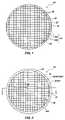
- FIG. 1is a top view of an exemplary semiconductor substrate, depicted as a wafer, which is shown as including a plurality of semiconductor devices on an active surface thereof;
- FIGS. 2 and 2Aare top views of the semiconductor substrate shown in FIG. 1 , with exemplary embodiments of support structures according to the present invention on the active surfaces thereof.
- FIG. 3is a cross-section taken along line 3 - 3 of FIG. 2 , depicting a first example of the manner in which the outer periphery of the support structure may be associated with an outer peripheral edge of the semiconductor substrate;
- FIGS. 4A through 4Dare cross-sections that are also taken along line 3 - 3 of FIG. 2 , illustrating second and third examples of the manner in which the outer periphery of the support structure may be associated with an outer peripheral edge of the semiconductor substrate;
- FIG. 5is a partial top view of the semiconductor substrate shown in FIG. 1 , depicting a variation of the support structure which includes a series of concentrically positioned upwardly protruding members, each of which extends along the full extent (e.g., length, circumference, etc.) of the support structure;
- FIG. 6is a cross-section taken along line 6 - 6 of FIG. 5 ;
- FIG. 7is a top view of the substrate shown in FIG. 1 , illustrating another exemplary embodiment of support structure that incorporates teachings of the present invention
- FIG. 8is an enlarged, partial cross-section taken along line 8 - 8 of FIG. 7 , showing a first example of the manner in which the outer periphery of the support structure may be associated with an outer peripheral edge of the semiconductor substrate;
- FIG. 9is also an enlarged, partial cross-section taken along line 8 - 8 of FIG. 7 , showing a second example of the manner in which the outer periphery of the support structure may be associated with an outer peripheral edge of the semiconductor substrate;
- FIG. 10is a schematic representation of an example of a layered manufacturing (e.g., stereolithography) apparatus that may be used to fabricate a support structure of the present invention upon an active surface of a semiconductor substrate;
- a layered manufacturinge.g., stereolithography
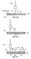
- FIGS. 11A through 11Eschematically depict use of the apparatus of FIG. 10 to fabricate the support structure shown in FIG. 4 upon the active surface of a semiconductor substrate;
- FIGS. 12A and 12Bschematically depict use of molding processes to form a support structure (e.g., that shown in FIG. 3 ) on the active surface of a semiconductor substrate;
- FIGS. 13A and 13Bschematically depict lamination of a preformed material film to the active surface of a semiconductor substrate and use of subtractive processes to remove material of the preformed film and to thereby form a support structure therefrom;
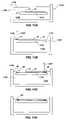
- FIGS. 14A and 14Bare schematic representations depicting thinning of a semiconductor substrate that has a support structure of the present invention secured to an active surface thereof;
- FIG. 15is a schematic representation of a method for transporting a thinned semiconductor substrate in accordance with teachings of the present invention.
- FIG. 16schematically depicts processing of a semiconductor substrate following thinning thereof.
- FIGS. 17A through 17Care schematic representations of a method for removing a support structure of the present invention from a thinned semiconductor substrate.
- semiconductor substrate 10may comprise a wafer of a semiconductor material, such as silicon, gallium arsenide, or indium phosphide.
- Semiconductor substrate 10includes two opposite major surfaces, one of which is commonly referred to in the art as an “active surface” 12 and the other of which is typically referred to in the art as a “back side” 16 (see FIGS. 3 , 4 A, 4 B, 6 , 8 , and 9 ). Both active surface 12 and back side 16 are bounded by an outer peripheral edge 18 of semiconductor substrate 10 . When semiconductor substrate 10 comprises a full wafer, as in the depicted example, outer peripheral edge 18 forms the circumference of the wafer.
- Edge bead removal area 20may be located on active surface 12 , adjacent to outer peripheral edge 18 .
- Edge bead removal area 20is a relatively narrow feature (e.g., three millimeters across) which may extend around the entire outer periphery of semiconductor substrate 10 .
- processing of semiconductor substrates 10 which lack edge bead removal areas 20is also within the scope of the present invention, although not specifically depicted in the drawings.
- semiconductor substrate 10may include a plurality of semiconductor devices 24 .
- Adjacent semiconductor devices 24are separated from one another by streets 30 , which extend across interior section 22 of active surface 12 , such as in the illustrated grid-like configuration.
- At least some of the semiconductor devices 24 that are located adjacent to outer peripheral edge 18 of semiconductor substrate 10comprise only blanks 24 p , while semiconductor devices 24 f are located somewhat internally from outer peripheral edge 18 .
- semiconductor substrate 10may lack semiconductor devices 24 on interior section 22 of active surface 12 thereof. This is because it may be desirable to thin a semiconductor substrate 10 prior to fabricating structures, such as semiconductor devices, thereon or therefrom. For example, the loss of semiconductor devices and the expenses incurred in fabricating the same may be avoided if a thinned semiconductor substrate 10 ′′ ( FIG. 14B ) without any semiconductor devices thereon breaks or is otherwise damaged during the thinning process. Alternatively, one entity may thin semiconductor substrates 10 , then provide the thinned semiconductor substrates 10 ′′ to one or more other entities for further processing (e.g., device fabrication).
- each semiconductor device 24includes one or more bond pads 27 ( FIGS. 8 and 9 ), which facilitate electrical communication with integrated circuitry of that semiconductor device 24 .
- FIGS. 2 through 4Ban example of a support structure according to the present invention, in this case a support ring 40 , 40 ′, 40 a ′, 40 b ′, 40 c ′ (shown in FIGS. 3 , 4 A, 4 B, 4 C, and 4 D, respectively) is depicted.
- support ring 40 , 40 ′, 40 a ′, 40 b ′, 40 c ′is positioned on active surface 12 of semiconductor substrate 10 , over edge bead removal area 20 thereof.
- Support ring 40 , 40 ′, 40 a ′, 40 b ′, 40 c ′extends completely around an outer periphery 13 of active surface 12 .
- An outer peripheral edge 42 , 42 ′ of support ring 40 , 40 ′, 40 a ′, 40 b ′, 40 c ′is in substantial alignment with ( FIG. 3 ) or is located outside ( FIGS. 4A and 4B ) of outer peripheral edge 18 .
- An interior edge 44 of support ring 40 , 40 ′, 40 a ′, 40 b ′, 40 c ′defines surfaces of an aperture 45 through support ring 40 , 40 ′, 40 a ′, 40 b ′, 40 c ′.
- Interior section 22 of active surface 12 and, thus, all of the semiconductor devices 24 f thereonare completely surrounded by interior edge 44 of support ring 40 , 40 ′, 40 a ′, 40 b ′, 40 c ′ and exposed through aperture 45 thereof.
- Support ring 40 , 40 ′, 40 a ′, 40 b ′, 40 c ′is formed from a material that is compatible with the material or materials of semiconductor substrate 10 .
- the material of support ring 40 , 40 ′, 40 a ′, 40 b ′, 40 c ′will, along with the thickness of support ring 40 , 40 ′, 40 a ′, 40 b ′, 40 c ′, impart a thinned semiconductor substrate 10 ′′ ( FIG. 14B ) with the desired amount of rigidity.
- support ring 40 , 40 ′, 40 a ′, 40 b ′, 40 c ′may be substantially impervious to chemicals (e.g., wet and dry etchants) that may be used in backgrinding processes, as well as compatible with conditions of any post-thinning processes.
- chemicalse.g., wet and dry etchants
- support ring 40 , 40 ′, 40 a ′, 40 b ′, 40 c ′may also facilitate or enhance sealing of support ring 40 , 40 ′, 40 a ′, 40 b ′, 40 c ′ to a support structure, such as a vacuum chuck, as semiconductor substrate 10 is being thinned or otherwise processed.
- support ring 40 , 40 ′, 40 a ′, 40 b ′, 40 c ′from a material that has a coefficient of thermal expansion (CTE) that is as close as possible to that of the material or materials from which semiconductor substrate 10 is formed (e.g., silicon has a CTE of about 2.9 ⁇ 10 ⁇ 6 /° C.), thereby preventing warpage of semiconductor substrate 10 and delamination of support ring 40 , 40 ′, 40 a ′, 40 b ′, 40 c ′ therefrom during processing of semiconductor substrate 10 (e.g., thinning or any processing that occurs thereafter).
- CTEcoefficient of thermal expansion
- Exemplary materials that may be used to form support ring 40 , 40 ′, 40 a ′, 40 b ′, 40 c ′include consolidatable materials that are useful in layered manufacturing processes (e.g., photoimageable polymers that are useful in stereolithography processes), photoresists, thermoset polymers (e.g., moldable silicones), and the like. While many of these materials may be less rigid than desired or have CTEs which differ significantly from the material or materials of semiconductor substrate 10 , fillers may be added thereto to impart the materials and, thus, support ring 40 , 40 ′, 40 a ′, 40 b ′, 40 c ′ with the desired properties.
- fillersexamples include, but are not limited to, silica (i.e., glass, silicon) particles, alumina (i.e., ceramic) particles, nitride (e.g., silicon nitride, boron nitride) particles, and polymeric particles or fibers (e.g., poly(p-phenyleneterephtalamide) fibers, which are marketed under the tradename KEVLAR® by E.I. du Pont de Nemours & Company of Wilmington, Del.).
- Photoimageable polymers that are useful in stereolithography processesmay have CTEs of about 55 ⁇ 10 ⁇ 6 /° C.
- a silica filler materialWhen a silica filler material is included therein, with the mixture including about 50%, by weight, photoimageable polymer and about 50%, by weight, silica particles, the CTE of the mixture is lowered significantly, to about 32 ⁇ 10 ⁇ 6 /° C. Fillers may also increase or enhance the fracture toughness (e.g., KEVLAR®), strength, rigidity, thermal properties (e.g., boron nitride), or structural integrity of the material (e.g., photoimageable polymer, photoresist, thermoset polymer, etc.) within which they are mixed.
- fracture toughnesse.g., KEVLAR®
- strengthe.g., rigidity
- thermal propertiese.g., boron nitride
- structural integrity of the materiale.g., photoimageable polymer, photoresist, thermoset polymer, etc.
- a support ring 40 , 40 ′, 40 a ′, 40 b ′, 40 c ′may have a width W which is at least as great as the width of edge bead removal area 20 (i.e., typically about 3 mm or more).
- the height H of support ring 40 , 40 ′, 40 a ′, 40 b ′, 40 c ′may impart support ring 40 , 40 ′, 40 a ′, 40 b ′, 40 c ′ and, thus, a thinned semiconductor substrate 10 ′′ ( FIG. 14B ) with which support ring 40 , 40 ′, 40 a ′, 40 b ′, 40 c ′ is to be used with a desired amount of rigidity.
- support ring 40 , 40 ′, 40 a ′, 40 b ′, 40 c ′may have a height of as small as about 25 ⁇ m (one mil) to about 200 ⁇ m (eight mils) or greater.
- the combined height H of support ring 40 , 40 ′, 40 a ′, 40 b ′, 40 c ′ and thickness of a thinned semiconductor substrate 10 ′′should not exceed the maximum substrate thickness (e.g., about 800 ⁇ m) that such equipment is configured to accommodate.
- the outer diameter (OD) of support ring 40 , 40 ′, 40 a ′, 40 b ′, 40 c ′should not exceed the maximum substrate diameter (e.g., 200 mm, 300 mm, etc.) that equipment for handling or processing a thinned semiconductor substrate 10 ′′ may be configured to accommodate.
- an outer peripheral edge 42 of support ring 40may be substantially coextensive and, thus, in substantial alignment with an outer peripheral edge 18 of semiconductor substrate 10 .
- a support ring 40 ′may extend beyond outer peripheral edge 18 of semiconductor substrate 10 , with an outer peripheral edge 42 ′ of a support ring 40 ′ being positioned outside of outer peripheral edge 18 of semiconductor substrate 10 . Accordingly, support ring 40 ′ includes an overhang region 46 ′, which is located beyond outer peripheral edge 18 of semiconductor substrate 10 .
- support ring 40 ′may include a circumferential support element 48 ′ beneath overhang region 46 ′, substantially coplanar with semiconductor substrate 10 , and in substantial contact with outer peripheral edge 18 .
- Circumferential support element 48 ′may have a height which is about the same as or less than the desired thickness of semiconductor substrate 10 following thinning thereof (i.e., the thickness of thinned semiconductor substrate 10 ′′ ( FIG. 14B ).
- Overhang region 46 ′ of support ring 40 ′ or a variation thereofmay include one or more ancillary features, such as one or more markings, locating features, or fixturing features.
- one or more dowel holes 55 , slots 56 , or fiducial marks 57may be formed on, in, or through overhang region 46 ′, as shown in FIG. 2A .
- the support ring 40 a ′ shown in FIG. 4Bincludes all of the features of support ring 40 ′, except for circumferential support element 48 ′ ( FIG. 4A ).
- FIG. 4CShown in FIG. 4C is another variation of support ring 40 b ′, which includes all of the features of support ring 40 ′ ( FIG. 4A ).
- Support ring 40 b ′differs from support ring 40 ′ in that circumferential support element 48 b ′ of support ring 40 b ′ extends from overhang region 46 ′ substantially to, as shown, or beyond a plane in which back side 16 of semiconductor substrate 10 is located.
- circumferential support element 48 b ′will protrude beyond back side 16 , forming a lip (not shown) that extends completely around outer peripheral edge 18 at back side 16 .
- a lipmay be useful for enhancing the rigidity of the thinned semiconductor substrate 10 ′′ (see FIG. 14B ), as well as for sealing back side 16 against a carrier while processing is being effected over active surface 12 of thinned semiconductor substrate 10 ′′.
- FIG. 4Dillustrates still another variation of support ring 40 c ′, which includes an overhang region 46 ′ and a circumferential support element 48 c ′.
- Circumferential support element 48 c ′differs from circumferential support element 48 ′ ( FIG. 4A ) in that circumferential support element 48 c ′ extends from overhang region 46 ′ to a location beyond a plane in which back side 16 of semiconductor substrate 10 is located.
- circumferential support element 48 c ′is spaced apart from outer peripheral edge 18 of semiconductor substrate 10 , providing a gap G that accommodates expansion or contraction of support ring 40 c ′ or semiconductor substrate 10 due to CTE mismatch therebetween.
- support ring 40 c ′also includes a retention ledge 49 ′ that extends inwardly from a lower edge of circumferential support element 48 c ′, along a plane which is parallel to a plane in which back side 16 of semiconductor substrate 10 is located, and over at least a peripheral portion 17 of back side 16 , thereby trapping outer peripheral edge 18 .
- support ring 40 ′′may comprise one or more sealing elements 50 ′′ which protrude from an upper surface 49 ′′ of support ring 40 ′′.
- Sealing elements 50 ′′are somewhat compliant features that are configured to facilitate the creation of a seal between upper surface 49 ′′ of support ring 40 ′′ and a surface or feature (not shown) against which support ring 40 ′′ is to be positioned, such as a surface of a sealing ring of a vacuum chuck.
- support members 140 , 140 ′are pictured in FIGS. 7 through 9 .
- support member 140 , 140 ′In addition to including an outer peripheral portion 150 , 150 ′ that covers an edge bead removal area 20 of active surface 12 of semiconductor substrate 10 , support member 140 , 140 ′ also includes an interior portion 160 , 160 ′ that forms protective structures 28 , 28 ′ over semiconductor devices 24 f that are carried by interior section 22 of active surface 12 .
- outer peripheral portion 150 , 150 ′ of support member 140 , 140 ′may be configured substantially the same as support rings 40 , 40 ′ depicted in FIGS. 3 and 4A , respectively.
- outer peripheral portion 150 , 150 ′ of support member 140 , 140 ′may include one or more sealing elements, such as the sealing elements 50 ′′ that are shown in FIGS. 5 and 6 .
- each protective structure 28 , 28 ′ of interior portion 160 , 160 ′ of support member 140 , 140 ′includes at least one aperture 162 , 162 ′ through which a corresponding bond pad 27 of the corresponding, underlying semiconductor device 24 f is exposed.
- FIG. 9shows a semiconductor substrate 10 ′ which includes trenches 32 at the locations of streets 30 , material of streets 30 having been removed by known processes, such as partial cutting with a wafer saw, photolithography (e.g., mask) and etch processes, or the like, to form trenches 32 .
- protective structure 28 ′covers an active surface 26 of each corresponding semiconductor device 24 f , as well as at least a portion of peripheral edges 25 thereof.
- support members 140 , 140 ′may be formed from a material which provides the desired degrees of rigidity and sealability. The thickness and other dimensions of support members 140 , 140 ′ may also factor into the rigidities thereof.
- support members 140 , 140 ′include protective structures 28 , 28 ′, the material from which support members 140 , 140 ′ also provides other desirable properties, such as a particular level of electrical insulation, an ability to withstand subsequent processing conditions (e.g., dicing, further packaging, etc.), an ability to withstand operating conditions (e.g., temperature) to which each semiconductor device 24 f is subjected when in use, a particular degree of impermeability to moisture, or the like.
- FIGS. 10 through 13Bvarious exemplary methods for forming support structures, including support rings 40 , 40 ′, 40 ′′ and support members 140 , 140 ′, are depicted. Although the description of these processes herein is limited to forming of a support ring 40 ′ ( FIGS. 11A through 12C ) or a support ring 40 ( FIGS. 13A and 13B ), they are also useful for forming other embodiments of support structures that incorporate teachings of the present invention.
- FIGS. 10 and 11A through 11 Eshow a layered manufacturing process that may be used to form a support ring 40 ′.
- FIG. 10an example of a stereolithography system 1000 , which effects a type of layered manufacturing process that employs selective irradiation of radiation-curable (e.g., by ultraviolet light, etc.) curable resin, is schematically represented.
- radiation-curablee.g., by ultraviolet light, etc.
- Stereolithography system 1000includes a fabrication tank 1100 and a material consolidation system 1200 , a machine vision system 1300 , a cleaning component 1400 , and a material reclamation system 1500 that are associated with fabrication tank 1100 .
- the depicted stereolithography system 1000also includes a substrate handling system 1600 , such as a rotary feed system or linear feed system available from Genmark Automation Inc. of Sunnyvale, Calif., for moving fabrication substrates (e.g., semiconductor substrates 10 ) from one system of stereolithography system 1000 to another.
- a substrate handling system 1600such as a rotary feed system or linear feed system available from Genmark Automation Inc. of Sunnyvale, Calif.
- fabrication substratese.g., semiconductor substrates 10
- controllers 1700such as computer processors or smaller groups of logic circuits, in such a way as to effect their operation in a desired manner.
- Controller 1700may comprise a computer or a computer processor, such as a so-called “microprocessor,” which may be programmed to effect a number of different functions. Alternatively, controller 1700 may be programmed to effect a specific set of related functions or even a single function. Each controller 1700 of stereolithography system 1000 may be associated with a single system thereof or a plurality of systems so as to orchestrate the operation of such systems relative to one another.
- Fabrication tank 1100includes a chamber 1110 which is configured to contain a support system 1130 .
- support system 1130is configured to carry one or more semiconductor substrates 10 .
- Fabrication tank 1100may also have a reservoir 1120 associated therewith.
- Reservoir 1120may be continuous with chamber 1110 .
- reservoir 1120may be separate from; but communicate with chamber 1110 in such a way as to provide unconsolidated material 1126 thereto.
- Reservoir 1120is configured to at least partially contain a volume 1124 of unconsolidated material 1126 , such as a photoimageable polymer, or “photopolymer,” particles of thermoplastic polymer, resin-coated particles, or the like.
- Photopolymers believed to be suitable for use with a stereolithography system 1000 and for fabricating support structures, such as support rings 40 ′, in accordance with teachings of the present inventioninclude, without limitation, Cibatool SL 5170, SL 5210, SL 5530, and SL 7510 resins. All of these photopolymers are available from Ciba Specialty Chemicals Inc. of Basel, Switzerland.
- Reservoir 1120 or another component associated with one or both of fabrication tank 1100 and reservoir 1120 thereofmay be configured to maintain a surface 1128 of a portion of volume 1124 located within chamber 1110 at a substantially constant elevation relative to chamber 1110 .
- a material consolidation system 1200is associated with fabrication tank 1100 in such a way as to direct consolidating energy 1220 into chamber 1110 thereof, toward at least areas of surface 1128 of volume 1124 of unconsolidated material 1126 within reservoir 1120 that are located over semiconductor substrate 10 .
- Consolidating energy 1220may comprise, for example, electromagnetic radiation of a selected wavelength or a range of wavelengths, an electron beam, or other suitable energy for consolidating unconsolidated material 1126 .
- Material consolidation system 1200includes a source 1210 of consolidating energy 1220 .
- source 1210 or a location control element 1212 associated therewithmay be configured to direct, or position, consolidating energy 1220 toward a plurality of desired areas of surface 1128 .
- a location control element 1212 associated therewithe.g., a set of galvanometers or mirrors, including one for x-axis movement and another for y-axis movement
- consolidating energy 1220remains relatively unfocused, it may be directed generally toward surface 1128 from a single, fixed location or from a plurality of different locations.
- operation of source 1210 , as well as movement thereof, if anymay be effected under the direction of controller 1700 .
- stereolithography system 1000may also include a machine vision system 1300 .
- Machine vision system 1300facilitates the direction of focused consolidating energy 1220 toward desired locations of features on semiconductor substrate 10 .
- operation of machine vision system 1300may be proscribed by controller 1700 . If any portion of machine vision system 1300 , such as a camera 1310 thereof, moves relative to chamber 1110 of fabrication tank 1100 , that portion of machine vision system 1300 may be positioned so as provide a clear path to all of the locations of surface 1128 that are located over each semiconductor substrate 10 within chamber 1110 .
- one or both of material consolidation system 1200(which may include a plurality of mirrors 1214 ) and machine vision system 1300 may be oriented and configured to operate in association with a plurality of fabrication tanks 1100 .
- one or more controllers 1700would be useful for orchestrating the operation of material consolidation system 1200 , machine vision system 1300 , and substrate handling system 1600 relative to a plurality of fabrication tanks 1100 .
- Cleaning component 1400 of stereolithography system 1000may also operate under the direction of controller 1700 .
- Cleaning component 1400 of stereolithography system 1000may be continuous with chamber 1110 of fabrication tank 1100 or positioned adjacent to fabrication tank 1100 . If cleaning component 1400 is continuous with chamber 1110 , any unconsolidated material 1126 that remains on a semiconductor substrate 10 may be removed therefrom prior to introduction of another semiconductor substrate 10 into chamber 1110 .
- cleaning component 1400is positioned adjacent to fabrication tank 1100 , residual unconsolidated material 1126 may be removed from a semiconductor substrate 10 as semiconductor substrate 10 is removed from chamber 1110 .
- any unconsolidated material 1126 remaining on semiconductor substrate 10may be removed therefrom after semiconductor substrate 10 has been removed from chamber 1110 , in which case the cleaning process may occur as another semiconductor substrate 10 is positioned within chamber 1110 .
- Material reclamation system 1500collects excess unconsolidated material 1126 that has been removed from a semiconductor substrate 10 by cleaning component 1400 , then returns the excess unconsolidated material 1126 to reservoir 1120 associated with fabrication tank 1100 .
- controller 1700under control of computer-aided drafting (CAD) or stereolithography (.stl) programming, may orchestrate operation of various components of stereolithography system 1000 to fabricate support structures, such as support rings 40 ′, as well as other features.
- CADcomputer-aided drafting
- .stlstereolithography
- FIGS. 11A through 11Edepict an example of the manner in which a support structure, such as support ring 40 ′, may be fabricated.
- semiconductor substrate 10is positioned on a support platen 1112 within chamber 1110 of fabrication tank 1100 ( FIG. 10 ). As depicted, semiconductor substrate 10 is submerged within volume 1124 of unconsolidated material 1126 so that unconsolidated material 1126 covers and fills all of the features that are located at active surface 12 of semiconductor substrate 10 .
- support platen 1112is raised such that the upper surface of semiconductor substrate 10 is brought to about the same level as (i.e., coplanar with) surface 1128 , as shown, or above surface 1128 of volume 1124 .
- Areas 1129 of unconsolidated material 1126 that are located adjacent to outer peripheral edge 18 of semiconductor substrate 10are then at least partially selectively consolidated (e.g., with a laser or other focused consolidating energy 1220 ) to initiate the formation of circumferential support element 48 ′ ( FIGS. 4A and 11C ) of support ring 40 ′ ( FIG. 4A ).
- This processmay be effected once if circumferential support element 48 ′ comprises a single material layer, or repeated multiple times, lowering semiconductor substrate 10 in multiple increments until active surface 12 thereof is substantially planar with surface 1128 of volume 1124 , if circumferential support element 48 ′ includes a plurality of superimposed, contiguous, mutually adhered layers of material.
- portions of support ring 40 ′ which are located above the plane in which active surface 12 of semiconductor substrate 10 is located, including overhang region 46 ′ thereof,may be fabricated, as shown in FIG. 11C .
- Support platen 1112is lowered such that active surface 12 is submerged beneath surface 1128 of volume 1124 a distance that, considering any change in the density of unconsolidated material 1126 upon consolidation thereof, will result in a layer or sublayer of consolidated material that protrudes above active surface 12 a desired height (e.g., about one mil, about four mils, about eight mils, etc.).
- Unconsolidated material 1126 at locations where the fabrication of a support structure, such as support ring 40 ′, is desiredmay then be selectively consolidated with focused consolidating energy 1220 (e.g., a laser beam) to form at least another layer of support ring 40 ′.
- focused consolidating energy 1220e.g., a laser beam
- these processesmay be repeated a number of times until a support structure, such as support ring 40 ′, and features thereof (e.g., the sealing elements 50 ′′ shown in FIGS. 5 and 6 , which may be formed as one or more separate layers from the remainder of support ring 40 ′) have been completely formed.
- a support structuresuch as support ring 40 ′, and features thereof (e.g., the sealing elements 50 ′′ shown in FIGS. 5 and 6 , which may be formed as one or more separate layers from the remainder of support ring 40 ′) have been completely formed.
- support platen 1112may be raised such that at least semiconductor substrate 10 and the support structure (e.g., support ring 40 ′) carried thereby are removed from volume 1124 of unconsolidated material 1126 , as shown in FIG. 11E . Thereafter, semiconductor substrate 10 and the support structure thereon may be cleaned, as known in the art.
- a support structure according to the present inventionmay be formed by applying a photoresist (e.g., by spin-on processes or otherwise, as known in the art) onto active surface 12 of semiconductor substrate 10 ( FIG. 1 ), then exposing desired regions of the photoresist to one or more suitable wavelengths of radiation (e.g., through a reticle), as in known photolithography processes, and developing the exposed regions with a chemical or chemicals that are suitable for consolidating the photoresist that has been exposed.
- a photoresiste.g., by spin-on processes or otherwise, as known in the art
- FIGS. 12A and 12Ban exemplary process for molding a support structure, such as a support ring 40 ′ ( FIGS. 4A and 12B ) in place upon a semiconductor substrate 10 is depicted.
- semiconductor substrate 10is positioned within a support cavity 212 of or otherwise supported by a first half 210 of a mold 200 , with active surface 12 of semiconductor substrate 10 remaining exposed. Thereafter, a second half 220 of mold 200 is then positioned over active surface 12 . Regions of active surface 12 , including edge bead removal area 20 thereof, upon which the support structure (e.g., support ring 40 ′) is to be positioned, communicate with one or more cavities 222 of second half 220 .
- first and second halves 210 , 220 of mold 200may include other features (e.g., runners, vents, etc.) that are positioned appropriately for the type of molding process in which mold 200 is to be used.
- known mold processese.g., transfer molding, pot molding, injection molding, etc.
- liquid mold materialfrom which the support structure (e.g., support ring 40 ′) is to be formed into each cavity 222 and onto regions of active surface 12 that communicate with each cavity 222 .
- semiconductor substrate 10 and the support structure (e.g., support ring 40 ′) that has been molded in place thereonmay be removed from mold 200 , as known in the art.
- FIGS. 13A and 13BAnother exemplary process for forming a support structure, such as support ring 40 ′ on at least an active surface 12 of a semiconductor substrate 10 is pictured in FIGS. 13A and 13B .
- a preformed sheet 300 of a material from which a support structure, such as support ring 40 ( FIG. 2 ), is to be formedis positioned over and secured to active surface 12 of semiconductor substrate 10 .
- Preformed sheet 300may be secured to active surface 12 by any technique which is compatible with the material of preformed sheet 300 and with semiconductor substrate 10 and semiconductor devices 24 ( FIGS. 1 and 2 ) that have been fabricated on active surface 12 thereof.
- preformed sheet 300may be secured to active surface 12 with a pressure-sensitive or curable adhesive, by heating preformed sheet 300 or active surface 12 , by applying solvent to at least a lower surface 302 of preformed sheet 300 or to active surface 12 , or by any other suitable process known in the art.
- a support structure(e.g., support ring 40 ) may be formed by the use of photolithography processes to form a mask 310 and removal of material through apertures 312 in mask 310 (e.g., with an etchant or solvent that is suitable for use in removing the material of preformed sheet 300 ), photoablation (e.g., which is useful with polymer films), or otherwise, as known in the art and suitable for use with the material of preformed sheet 300 and with semiconductor substrate 10 and semiconductor devices 24 ( FIGS. 1 and 2 ) that have been fabricated on active surface 12 thereof.
- Mask 310may then be removed by way of known resist strip processes.
- a support ring 40 , 40 ′, 40 a ′, 40 b ′, 40 c ′, 40 ′′may be formed separately from a semiconductor substrate 10 ( FIG.
- support ring 40 c ′may be formed in two or more pieces
- semiconductor substrate 10and, in the case of support ring 40 c ′, pieces are assembled with one another
- securedi.e., adhered
- uncured polymere.g., thermoset polymer or photopolymer
- FIGS. 14A and 14Bthinning of back side 16 of semiconductor substrate 10 is schematically depicted.
- FIGS. 14A and 14Billustrate backgrinding of a semiconductor substrate 10 that includes a support ring 40 on at least active surface 12 thereof, backgrinding may also be effected with another embodiment of support structure of the present invention on at least active surface 12 , as well as with another embodiment of semiconductor substrate (e.g., semiconductor substrate 10 ′, shown in FIG. 9 ).
- semiconductor substrate 10is positioned active surface 12 -down over a carrier 400 , for example, a vacuum chuck available from Semitool, Inc. of Kalispell, Mont.
- the support structuree.g., support ring 40
- active surface 12 of semiconductor substrate 10contacts a surface 410 of carrier 400 or a corresponding feature (e.g., an O-ring 412 ) thereon, and may form a seal thereagainst.
- Known processese.g., application of a negative pressure N to active surface 12 of semiconductor substrate 10 may be used to secure semiconductor substrate 10 against surface 410 or a feature (e.g., o-ring 412 ) thereon and, optionally, to seal active surface 12 from exposure to conditions that are present at the exterior (e.g., back side 16 and outer peripheral edge 18 ) of semiconductor substrate 10 .
- known techniquesmay be used to remove material from back side 16 of semiconductor substrate 10 and, thus, to thin semiconductor substrate 10 to a desired thickness, as depicted in FIG. 14B .
- known mechanical backgrinding or polishing processese.g., mechanical lapping techniques
- chemical backgrinding or polishing processese.g., wet etch processes, dry etch processes, such as that described in U.S. Pat. No. 6,498,074 to Siniaguine et al., the disclosure of which is hereby incorporated herein in its entirety by this reference, etc.
- a combination of mechanical and chemical backgrinding or polishing processesmay be employed to thin semiconductor substrate 10 .
- Such thinning processesmay be effected until the resulting thinned semiconductor substrate 10 ′′ has a desired thickness (e.g., a thickness of about 230 ⁇ m or less, a thickness of about 50 ⁇ m or less, etc.).
- a thinned semiconductor substrate 10 ′′which includes a support structure, such as support ring 40 , on at least active surface 12 thereof, is shown in FIG. 14B .
- FIG. 15schematically depicts thinned semiconductor substrates 10 ′′ of the present invention in substrate cartridges 510 of a multi-substrate cassette 500 .
- cassette 500includes a plurality of substrate cartridges 510 , each of which is somewhat horizontally oriented and configured to receive a semiconductor substrate of standard dimensions (e.g., a 200 mm or 300 mm silicon wafer that has not been thinned).
- Substrates, including thinned semiconductor substrates 10 ′′ that incorporate teachings of the present invention,may be introduced into and removed from substrate cartridges 510 , as known in the art (e.g., with robotic handling equipment).
- one or more thinned semiconductor substrates 10 ′′may be transported from process equipment in which backgrinding or thinning is effected to equipment by which thinned semiconductor substrates 10 ′′ will be further processed.
- thinned semiconductor substrates 10 ′′may be secured (e.g., with adhesive materials) to other substrates, such as insulators like ceramic, glass, or sapphire, to form silicon-on-insulator (SOI) type substrates, such as a silicon-on-ceramic (SOC), silicon-on-glass (SOG), silicon-on-sapphire (SOS), or similar substrates.
- SOIsilicon-on-insulator
- semiconductor devices 24 f that are carried by active surface 12 of a thinned semiconductor substrate 10 ′′may be packaged by known wafer level packaging (WLP) processes (e.g., by stereolithography, by use of known layer formation and patterning processes, etc.), which typically include the formation of protective structures 28 ′′ over each semiconductor device 24 f.
- WLPwafer level packaging
- FIGS. 17A through 17Care schematic representations of a method for removing a support structure of the present invention, such as a support ring 40 , 40 ′, 40 a ′, 40 b ′, 40 c ′, 40 ′′, as shown in FIG. 17A , a support member 140 , as shown in FIG. 17B , or a support member 140 ′, as shown in FIG. 17C , from a thinned semiconductor substrate 10 ′′.
- known dicing processesmay be used to singulate semiconductor devices 24 f from thinned semiconductor substrate 10 ′′. Since support ring 40 , 40 ′, 40 ′′ does not cover any of the semiconductor devices 24 f that are carried by active surface 12 ′ of thinned semiconductor substrate 10 ′′, support ring 40 , 40 ′, 40 ′′ will remain on the fragments 124 p ′ that result from the dicing process, with each of the resulting semiconductor dice 124 ′ being substantially bare (e.g., active surfaces 12 ′ thereof remaining exposed).
- the support structurecomprises a support structure (e.g., support member 140 ) that includes an interior portion (e.g., interior portion 160 ) that covers portions of the active surfaces 12 ′ of semiconductor devices 24 f
- dicing, or singulationof the semiconductor devices 24 f from one another proceeds through both the interior portion and thinned semiconductor substrate 10 ′′.
- the result of such dicing, or singulationis a plurality of low-profile packaged semiconductor devices 123 ′.
- FIG. 17Cillustrates dicing, or singulation, of a thinned semiconductor substrate 10 ′ that includes trenches 32 along streets 30 between adjacent semiconductor devices 24 f as well as a support member 140 ′ substantially covering active surfaces 12 ′ thereof.
- trenches 32 and material of protective structures 28 ′may be exposed through back side 16 of semiconductor substrate 10 ′, effectively separating semiconductor devices 24 f from one another. Nonetheless, protective structures 28 ′, which comprise portions of interior portion 160 ′ of support member 140 ′, remain connected to one another, preventing the physical separation of semiconductor devices 24 f from each another.
- Support member 140 ′may be diced, or singulated, as known in the art, such as by use of the illustrated wafer saw 600 .
- peripheral edges 125 of each singulated semiconductor die 124 ′will be at least partially covered with peripheral portions 129 ′ of singulated protective structures 128 ′, each of these elements together forming a low-profile packaged semiconductor device 123 ′.
- semiconductor devices 24 fFIGS. 17A through 17C ) have been physically separated from one another, further processing may occur, such as the selection of known good dice (KGDs), the connection thereof to one or more other semiconductor device components (e.g., a carrier substrate, an interposer, another semiconductor device, etc.), the incorporation thereof into a stacked multi-chip module (MCM) of standard dimensions but increased chip density, or packaging thereof with one or more other semiconductor device components may be conducted, as known in the art.
- GMDsknown good dice
- MCMstacked multi-chip module
Landscapes
- Chemical & Material Sciences (AREA)
- Engineering & Computer Science (AREA)
- Manufacturing & Machinery (AREA)
- Materials Engineering (AREA)
- Ceramic Engineering (AREA)
- Civil Engineering (AREA)
- Composite Materials (AREA)
- Structural Engineering (AREA)
- Physics & Mathematics (AREA)
- General Physics & Mathematics (AREA)
- Mechanical Treatment Of Semiconductor (AREA)
- Container, Conveyance, Adherence, Positioning, Of Wafer (AREA)
Abstract
Description
Claims (16)
Priority Applications (6)
| Application Number | Priority Date | Filing Date | Title |
|---|---|---|---|
| US10/666,742US7713841B2 (en) | 2003-09-19 | 2003-09-19 | Methods for thinning semiconductor substrates that employ support structures formed on the substrates |
| US10/928,381US20050064679A1 (en) | 2003-09-19 | 2004-08-27 | Consolidatable composite materials, articles of manufacture formed therefrom, and fabrication methods |
| US11/216,938US20060008739A1 (en) | 2003-09-19 | 2005-08-31 | Materials for use in programmed material consolidation processes |
| US11/216,617US7960829B2 (en) | 2003-09-19 | 2005-08-31 | Support structure for use in thinning semiconductor substrates and for supporting thinned semiconductor substrates |
| US11/216,599US20060003255A1 (en) | 2003-09-19 | 2005-08-31 | Methods for optimizing physical characteristics of selectively consolidatable materials |
| US11/216,866US20060003549A1 (en) | 2003-09-19 | 2005-08-31 | Assemblies including semiconductor substrates of reduced thickness and support structures therefor |
Applications Claiming Priority (1)
| Application Number | Priority Date | Filing Date | Title |
|---|---|---|---|
| US10/666,742US7713841B2 (en) | 2003-09-19 | 2003-09-19 | Methods for thinning semiconductor substrates that employ support structures formed on the substrates |
Related Child Applications (5)
| Application Number | Title | Priority Date | Filing Date |
|---|---|---|---|
| US10/928,381Continuation-In-PartUS20050064679A1 (en) | 2003-09-19 | 2004-08-27 | Consolidatable composite materials, articles of manufacture formed therefrom, and fabrication methods |
| US11/216,938DivisionUS20060008739A1 (en) | 2003-09-19 | 2005-08-31 | Materials for use in programmed material consolidation processes |
| US11/216,599DivisionUS20060003255A1 (en) | 2003-09-19 | 2005-08-31 | Methods for optimizing physical characteristics of selectively consolidatable materials |
| US11/216,866DivisionUS20060003549A1 (en) | 2003-09-19 | 2005-08-31 | Assemblies including semiconductor substrates of reduced thickness and support structures therefor |
| US11/216,617DivisionUS7960829B2 (en) | 2003-09-19 | 2005-08-31 | Support structure for use in thinning semiconductor substrates and for supporting thinned semiconductor substrates |
Publications (2)
| Publication Number | Publication Date |
|---|---|
| US20050064681A1 US20050064681A1 (en) | 2005-03-24 |
| US7713841B2true US7713841B2 (en) | 2010-05-11 |
Family
ID=34313183
Family Applications (5)
| Application Number | Title | Priority Date | Filing Date |
|---|---|---|---|
| US10/666,742Expired - LifetimeUS7713841B2 (en) | 2003-09-19 | 2003-09-19 | Methods for thinning semiconductor substrates that employ support structures formed on the substrates |
| US11/216,938AbandonedUS20060008739A1 (en) | 2003-09-19 | 2005-08-31 | Materials for use in programmed material consolidation processes |
| US11/216,866AbandonedUS20060003549A1 (en) | 2003-09-19 | 2005-08-31 | Assemblies including semiconductor substrates of reduced thickness and support structures therefor |
| US11/216,617Expired - Fee RelatedUS7960829B2 (en) | 2003-09-19 | 2005-08-31 | Support structure for use in thinning semiconductor substrates and for supporting thinned semiconductor substrates |
| US11/216,599AbandonedUS20060003255A1 (en) | 2003-09-19 | 2005-08-31 | Methods for optimizing physical characteristics of selectively consolidatable materials |
Family Applications After (4)
| Application Number | Title | Priority Date | Filing Date |
|---|---|---|---|
| US11/216,938AbandonedUS20060008739A1 (en) | 2003-09-19 | 2005-08-31 | Materials for use in programmed material consolidation processes |
| US11/216,866AbandonedUS20060003549A1 (en) | 2003-09-19 | 2005-08-31 | Assemblies including semiconductor substrates of reduced thickness and support structures therefor |
| US11/216,617Expired - Fee RelatedUS7960829B2 (en) | 2003-09-19 | 2005-08-31 | Support structure for use in thinning semiconductor substrates and for supporting thinned semiconductor substrates |
| US11/216,599AbandonedUS20060003255A1 (en) | 2003-09-19 | 2005-08-31 | Methods for optimizing physical characteristics of selectively consolidatable materials |
Country Status (1)
| Country | Link |
|---|---|
| US (5) | US7713841B2 (en) |
Cited By (4)
| Publication number | Priority date | Publication date | Assignee | Title |
|---|---|---|---|---|
| US20100244161A1 (en)* | 2007-11-30 | 2010-09-30 | Skyworks Solutions, Inc. | Wafer level packaging using flip chip mounting |
| US20100283144A1 (en)* | 2007-12-26 | 2010-11-11 | Steve Xin Liang | In-situ cavity circuit package |
| US20170263480A1 (en)* | 2013-04-11 | 2017-09-14 | Infineon Technologies Ag | Arrangement having a plurality of chips and a chip carrier, and a processing arrangement |
| US11594445B2 (en) | 2018-03-13 | 2023-02-28 | Applied Materials, Inc. | Support ring with plasma spray coating |
Families Citing this family (35)
| Publication number | Priority date | Publication date | Assignee | Title |
|---|---|---|---|---|
| US6740962B1 (en)* | 2000-02-24 | 2004-05-25 | Micron Technology, Inc. | Tape stiffener, semiconductor device component assemblies including same, and stereolithographic methods for fabricating same |
| US7198055B2 (en)* | 2002-09-30 | 2007-04-03 | Lam Research Corporation | Meniscus, vacuum, IPA vapor, drying manifold |
| US20050064683A1 (en)* | 2003-09-19 | 2005-03-24 | Farnworth Warren M. | Method and apparatus for supporting wafers for die singulation and subsequent handling |
| US20050064679A1 (en)* | 2003-09-19 | 2005-03-24 | Farnworth Warren M. | Consolidatable composite materials, articles of manufacture formed therefrom, and fabrication methods |
| US7713841B2 (en) | 2003-09-19 | 2010-05-11 | Micron Technology, Inc. | Methods for thinning semiconductor substrates that employ support structures formed on the substrates |
| US7468969B2 (en)* | 2003-11-07 | 2008-12-23 | Interdigital Technology Corporation | Apparatus and methods for central control of mesh networks |
| US7186629B2 (en)* | 2003-11-19 | 2007-03-06 | Advanced Materials Sciences, Inc. | Protecting thin semiconductor wafers during back-grinding in high-volume production |
| US7244665B2 (en)* | 2004-04-29 | 2007-07-17 | Micron Technology, Inc. | Wafer edge ring structures and methods of formation |
| US7547978B2 (en) | 2004-06-14 | 2009-06-16 | Micron Technology, Inc. | Underfill and encapsulation of semiconductor assemblies with materials having differing properties |
| US7235431B2 (en) | 2004-09-02 | 2007-06-26 | Micron Technology, Inc. | Methods for packaging a plurality of semiconductor dice using a flowable dielectric material |
| US20060211233A1 (en)* | 2005-03-21 | 2006-09-21 | Skyworks Solutions, Inc. | Method for fabricating a wafer level package having through wafer vias for external package connectivity and related structure |
| US8124455B2 (en)* | 2005-04-02 | 2012-02-28 | Stats Chippac Ltd. | Wafer strength reinforcement system for ultra thin wafer thinning |
| US20070045807A1 (en)* | 2005-09-01 | 2007-03-01 | Micron Technology, Inc. | Microelectronic devices and methods for manufacturing microelectronic devices |
| US8202460B2 (en)* | 2005-09-22 | 2012-06-19 | International Business Machines Corporation | Microelectronic substrate having removable edge extension element |
| US7846776B2 (en)* | 2006-08-17 | 2010-12-07 | Micron Technology, Inc. | Methods for releasably attaching sacrificial support members to microfeature workpieces and microfeature devices formed using such methods |
| SG143098A1 (en) | 2006-12-04 | 2008-06-27 | Micron Technology Inc | Packaged microelectronic devices and methods for manufacturing packaged microelectronic devices |
| US7988794B2 (en)* | 2007-02-07 | 2011-08-02 | Infineon Technologies Ag | Semiconductor device and method |
| US7662669B2 (en)* | 2007-07-24 | 2010-02-16 | Northrop Grumman Space & Mission Systems Corp. | Method of exposing circuit lateral interconnect contacts by wafer saw |
| US7923298B2 (en) | 2007-09-07 | 2011-04-12 | Micron Technology, Inc. | Imager die package and methods of packaging an imager die on a temporary carrier |
| US9117828B2 (en)* | 2009-03-27 | 2015-08-25 | Taiwan Semiconductor Manufacturing Company, Ltd. | Method of handling a thin wafer |
| US8062958B2 (en)* | 2009-04-01 | 2011-11-22 | Micron Technology, Inc. | Microelectronic device wafers and methods of manufacturing |
| US8823154B2 (en)* | 2009-05-08 | 2014-09-02 | The Regents Of The University Of California | Encapsulation architectures for utilizing flexible barrier films |
| US20110221053A1 (en)* | 2010-03-11 | 2011-09-15 | Qualcomm Incorporated | Pre-processing to reduce wafer level warpage |
| TWI505342B (en)* | 2010-09-02 | 2015-10-21 | United Microelectronics Corp | Method for thinning wafer |
| US8278189B2 (en)* | 2010-09-02 | 2012-10-02 | United Microelectronics Corp. | Method for thinning wafer |
| CN102403193A (en)* | 2010-09-17 | 2012-04-04 | 联华电子股份有限公司 | Methods of Thinning Wafers |
| US8580615B2 (en)* | 2011-02-18 | 2013-11-12 | Applied Materials, Inc. | Method and system for wafer level singulation |
| US8461019B2 (en)* | 2011-07-19 | 2013-06-11 | Disco Corporation | Method of processing device wafer |
| US8580655B2 (en)* | 2012-03-02 | 2013-11-12 | Disco Corporation | Processing method for bump-included device wafer |
| TWM464809U (en)* | 2012-10-20 | 2013-11-01 | Applied Materials Inc | Focus ring segment and assembly |
| US9589880B2 (en)* | 2013-10-09 | 2017-03-07 | Infineon Technologies Ag | Method for processing a wafer and wafer structure |
| US20150371956A1 (en)* | 2014-06-19 | 2015-12-24 | Globalfoundries Inc. | Crackstops for bulk semiconductor wafers |
| US20180122670A1 (en)* | 2016-11-01 | 2018-05-03 | Varian Semiconductor Equipment Associates, Inc. | Removable substrate plane structure ring |
| US10546916B2 (en)* | 2018-06-29 | 2020-01-28 | Intel Corporation | Package-integrated vertical capacitors and methods of assembling same |
| JP7323937B2 (en)* | 2020-05-22 | 2023-08-09 | アピックヤマダ株式会社 | Resin molding equipment |
Citations (78)
| Publication number | Priority date | Publication date | Assignee | Title |
|---|---|---|---|---|
| US3976288A (en) | 1975-11-24 | 1976-08-24 | Ibm Corporation | Semiconductor wafer dicing fixture |
| US4266334A (en) | 1979-07-25 | 1981-05-12 | Rca Corporation | Manufacture of thinned substrate imagers |
| EP0023231B1 (en) | 1979-07-27 | 1982-08-11 | Tabarelli, Werner, Dr. | Optical lithographic method and apparatus for copying a pattern onto a semiconductor wafer |
| US4925515A (en) | 1987-11-27 | 1990-05-15 | Takatori Corporation | Method and apparatus for applying a protective tape on a wafer and cutting it out to shape |
| US5114880A (en) | 1990-06-15 | 1992-05-19 | Motorola, Inc. | Method for fabricating multiple electronic devices within a single carrier structure |
| US5121256A (en) | 1991-03-14 | 1992-06-09 | The Board Of Trustees Of The Leland Stanford Junior University | Lithography system employing a solid immersion lens |
| US5268065A (en) | 1992-12-21 | 1993-12-07 | Motorola, Inc. | Method for thinning a semiconductor wafer |
| US5460703A (en) | 1992-11-12 | 1995-10-24 | Applied Materials, Inc. | Low thermal expansion clamping mechanism |
| US5547906A (en) | 1992-09-14 | 1996-08-20 | Badehi; Pierre | Methods for producing integrated circuit devices |
| US5610683A (en) | 1992-11-27 | 1997-03-11 | Canon Kabushiki Kaisha | Immersion type projection exposure apparatus |
| US5675402A (en) | 1994-10-21 | 1997-10-07 | Hyundai Electronics Industries Co., Ltd. | Stepper light control using movable blades |
| US5703493A (en) | 1995-10-25 | 1997-12-30 | Motorola, Inc. | Wafer holder for semiconductor applications |
| US5705016A (en) | 1994-11-29 | 1998-01-06 | Lintec Corporation | Method of preventing transfer of adhesive substance to dicing ring frame, pressure-sensitive adhesive sheet for use in the method and wafer working sheet having the pressure-sensitive adhesive sheet |
| US5723385A (en) | 1996-12-16 | 1998-03-03 | Taiwan Semiconductor Manufacturing Company, Ltd | Wafer edge seal ring structure |
| US5803797A (en) | 1996-11-26 | 1998-09-08 | Micron Technology, Inc. | Method and apparatus to hold intergrated circuit chips onto a chuck and to simultaneously remove multiple intergrated circuit chips from a cutting chuck |
| US5824457A (en) | 1996-10-02 | 1998-10-20 | Taiwan Semiconductor Manufacturing Company, Ltd. | Use of WEE (wafer edge exposure) to prevent polyimide contamination |
| US5827394A (en) | 1996-07-15 | 1998-10-27 | Vanguard International Semiconductor Corporation | Step and repeat exposure method for loosening integrated circuit dice from a radiation sensitive adhesive tape backing |
| US5833869A (en) | 1995-05-30 | 1998-11-10 | Motorola Inc. | Method for etching photolithographically produced quartz crystal blanks for singulation |
| US5843527A (en) | 1995-06-15 | 1998-12-01 | Dainippon Screen Mfg. Co., Ltd. | Coating solution applying method and apparatus |
| US5869354A (en)* | 1992-04-08 | 1999-02-09 | Elm Technology Corporation | Method of making dielectrically isolated integrated circuit |
| US5919520A (en) | 1996-08-30 | 1999-07-06 | Tokyo Electron Limited | Coating method and apparatus for semiconductor process |
| US6033589A (en) | 1997-09-30 | 2000-03-07 | Taiwan Semiconductor Manufacturing Co., Ltd. | Method for depositing a coating layer on a wafer without edge bead formation |
| US6040248A (en) | 1998-06-24 | 2000-03-21 | Taiwan Semiconductor Manufacturing Company | Chemistry for etching organic low-k materials |
| US6039830A (en) | 1997-07-25 | 2000-03-21 | Samsung Electronics Co., Ltd. | Method of and apparatus for laminating a semiconductor wafer with protective tape |
| US6042976A (en) | 1999-02-05 | 2000-03-28 | Taiwan Semiconductor Manufacturing Company, Ltd. | Method of calibrating WEE exposure tool |
| US6048948A (en) | 1994-09-07 | 2000-04-11 | Mazda Motor Corporation | Method for producing a polymer composite material |
| US6111306A (en) | 1993-12-06 | 2000-08-29 | Fujitsu Limited | Semiconductor device and method of producing the same and semiconductor device unit and method of producing the same |
| US6114253A (en) | 1999-03-15 | 2000-09-05 | Taiwan Semiconductor Manufacturing Company | Via patterning for poly(arylene ether) used as an inter-metal dielectric |
| US6140151A (en) | 1998-05-22 | 2000-10-31 | Micron Technology, Inc. | Semiconductor wafer processing method |
| US6143590A (en) | 1994-09-08 | 2000-11-07 | Fujitsu Limited | Multi-chip semiconductor device and method of producing the same |
| US6150240A (en) | 1998-07-27 | 2000-11-21 | Motorola, Inc. | Method and apparatus for singulating semiconductor devices |
| US6245646B1 (en) | 1999-04-16 | 2001-06-12 | Micron Technology, Inc. | Film frame substrate fixture |
| US6251488B1 (en) | 1999-05-05 | 2001-06-26 | Optomec Design Company | Precision spray processes for direct write electronic components |
| US6259962B1 (en) | 1999-03-01 | 2001-07-10 | Objet Geometries Ltd. | Apparatus and method for three dimensional model printing |
| US6268584B1 (en) | 1998-01-22 | 2001-07-31 | Optomec Design Company | Multiple beams and nozzles to increase deposition rate |
| US6303469B1 (en) | 2000-06-07 | 2001-10-16 | Micron Technology, Inc. | Thin microelectronic substrates and methods of manufacture |
| US6323295B1 (en) | 1995-02-09 | 2001-11-27 | Ciba Specialty Chemicals Corporation | Polymerizable composition, process for producing cross-linked polymers and crosslinkable polymers |
| US6322598B1 (en) | 1998-07-30 | 2001-11-27 | Imec Vzw | Semiconductor processing system for processing discrete pieces of substrate to form electronic devices |
| US6326698B1 (en) | 2000-06-08 | 2001-12-04 | Micron Technology, Inc. | Semiconductor devices having protective layers thereon through which contact pads are exposed and stereolithographic methods of fabricating such semiconductor devices |
| US6339255B1 (en) | 1998-10-24 | 2002-01-15 | Hyundai Electronics Industries Co., Ltd. | Stacked semiconductor chips in a single semiconductor package |
| US6344402B1 (en) | 1999-07-28 | 2002-02-05 | Disco Corporation | Method of dicing workpiece |
| US6391251B1 (en) | 1999-07-07 | 2002-05-21 | Optomec Design Company | Forming structures from CAD solid models |
| US6399464B1 (en) | 1998-02-23 | 2002-06-04 | Micron Technology, Inc. | Packaging die preparation |
| US6413150B1 (en) | 1999-05-27 | 2002-07-02 | Texas Instruments Incorporated | Dual dicing saw blade assembly and process for separating devices arrayed a substrate |
| US20020091173A1 (en) | 1999-06-14 | 2002-07-11 | Nitto Denko Corporation | Re-release adhesive and re-release adhesive sheet |
| US6432752B1 (en) | 2000-08-17 | 2002-08-13 | Micron Technology, Inc. | Stereolithographic methods for fabricating hermetic semiconductor device packages and semiconductor devices including stereolithographically fabricated hermetic packages |
| US6462273B1 (en) | 2001-03-16 | 2002-10-08 | Micron Technology, Inc. | Semiconductor card and method of fabrication |
| US6462401B2 (en) | 2000-03-27 | 2002-10-08 | Nec Corporation | Semiconductor wafer having a bank on a scribe line |
| US6465329B1 (en) | 1999-01-20 | 2002-10-15 | Amkor Technology, Inc. | Microcircuit die-sawing protector and method |
| US6468832B1 (en) | 2000-07-19 | 2002-10-22 | National Semiconductor Corporation | Method to encapsulate bumped integrated circuit to create chip scale package |
| US6471806B1 (en) | 1997-06-05 | 2002-10-29 | Texas Instruments Incorporated | Method of adhering a wafer to wafer tape |
| US20020171177A1 (en) | 2001-03-21 | 2002-11-21 | Kritchman Elisha M. | System and method for printing and supporting three dimensional objects |
| US6486939B2 (en) | 1998-10-19 | 2002-11-26 | Vanguard International Semiconductor Corporation | Electronically controlled universal phase-shifting mask for stepper exposure system |
| US6489042B2 (en) | 1998-12-23 | 2002-12-03 | 3M Innovative Properties Company | Photoimageable dielectric material for circuit protection |
| US6498074B2 (en) | 1996-10-29 | 2002-12-24 | Tru-Si Technologies, Inc. | Thinning and dicing of semiconductor wafers using dry etch, and obtaining semiconductor chips with rounded bottom edges and corners |
| US20030003688A1 (en) | 2000-08-25 | 2003-01-02 | Tandy William D. | Method and apparatus for marking a bare semiconductor die |
| US6506688B2 (en) | 2001-01-24 | 2003-01-14 | Macronix International Co., Inc. | Method for removing photoresist layer on wafer edge |
| US6537482B1 (en) | 2000-08-08 | 2003-03-25 | Micron Technology, Inc. | Underfill and encapsulation of carrier substrate-mounted flip-chip components using stereolithography |
| US20030059708A1 (en) | 2000-06-09 | 2003-03-27 | Tetsuya Yamamura | Resin composition and three-dimensional object |
| US6551906B2 (en) | 2000-07-06 | 2003-04-22 | Oki Electric Industry Co., Ltd. | Method of fabricating semiconductor device |
| US20030077399A1 (en) | 2001-10-23 | 2003-04-24 | Potyrailo Radislav Alexandrovich | Systems and methods for the deposition and curing of coating compositions |
| US6562661B2 (en)* | 2000-02-24 | 2003-05-13 | Micron Technology, Inc. | Tape stiffener, semiconductor device component assemblies including same, and stereolithographic methods for fabricating same |
| US6582983B1 (en) | 2002-07-12 | 2003-06-24 | Keteca Singapore Singapore | Method and wafer for maintaining ultra clean bonding pads on a wafer |
| US6589818B2 (en) | 1995-05-18 | 2003-07-08 | Hitachi. Ltd. | Method for mounting a thin semiconductor device |
| US20030151167A1 (en) | 2002-01-03 | 2003-08-14 | Kritchman Eliahu M. | Device, system and method for accurate printing of three dimensional objects |
| US6621161B2 (en) | 1999-03-30 | 2003-09-16 | Mitsubishi Denki Kabushiki Kaisha | Semiconductor device having a package structure |
| US6680241B2 (en) | 2000-07-25 | 2004-01-20 | Fujitsu Limited | Method of manufacturing semiconductor devices by dividing wafer into chips and such semiconductor devices |
| US6683378B2 (en) | 2001-08-30 | 2004-01-27 | Micron Technology, Inc. | System for singulating semiconductor components utilizing alignment pins |
| US6686225B2 (en) | 2001-07-27 | 2004-02-03 | Texas Instruments Incorporated | Method of separating semiconductor dies from a wafer |
| US6736896B2 (en) | 2002-10-10 | 2004-05-18 | Taiwan Semiconductor Manufacturing Co., Ltd | Gas spray arm for spin coating apparatus |
| US20040229002A1 (en) | 2003-05-15 | 2004-11-18 | 3D Systems, Inc. | Stereolithographic seal and support structure for semiconductor wafer |
| US20050064681A1 (en) | 2003-09-19 | 2005-03-24 | Wood Alan G. | Support structure for thinning semiconductor substrates and thinning methods employing the support structure |
| US6908784B1 (en) | 2002-03-06 | 2005-06-21 | Micron Technology, Inc. | Method for fabricating encapsulated semiconductor components |
| US6940181B2 (en) | 2003-10-21 | 2005-09-06 | Micron Technology, Inc. | Thinned, strengthened semiconductor substrates and packages including same |
| US6974721B2 (en) | 2002-09-26 | 2005-12-13 | Shinko Electric Industries Co., Ltd. | Method for manufacturing thin semiconductor chip |
| US20060109630A1 (en) | 2004-11-19 | 2006-05-25 | Colgan Evan G | Apparatus and methods for cooling semiconductor integrated circuit package structures |
| US7118938B2 (en) | 2002-12-30 | 2006-10-10 | Dongbu Electronics Co., Ltd. | Method for packaging a multi-chip module of a semiconductor device |
| US7140951B2 (en) | 2003-01-10 | 2006-11-28 | Kabushiki Kaisha Toshiba | Semiconductor device manufacturing apparatus and semiconductor device manufacturing method for forming semiconductor chips by dividing semiconductor wafer |
Family Cites Families (14)
| Publication number | Priority date | Publication date | Assignee | Title |
|---|---|---|---|---|
| US6018463A (en)* | 1997-08-22 | 2000-01-25 | Raytheon Company | Large non-hermetic multichip module package |
| US6217972B1 (en)* | 1997-10-17 | 2001-04-17 | Tessera, Inc. | Enhancements in framed sheet processing |
| JP4087000B2 (en)* | 1999-03-08 | 2008-05-14 | 日鉱金属株式会社 | Ladle and ladle lining method |
| WO2000059036A1 (en)* | 1999-03-26 | 2000-10-05 | Hitachi, Ltd. | Semiconductor module and method of mounting |
| US6617671B1 (en)* | 1999-06-10 | 2003-09-09 | Micron Technology, Inc. | High density stackable and flexible substrate-based semiconductor device modules |
| US6198163B1 (en)* | 1999-10-18 | 2001-03-06 | Amkor Technology, Inc. | Thin leadframe-type semiconductor package having heat sink with recess and exposed surface |
| US6582938B1 (en)* | 2001-05-11 | 2003-06-24 | Affymetrix, Inc. | Amplification of nucleic acids |
| US6461881B1 (en)* | 2000-06-08 | 2002-10-08 | Micron Technology, Inc. | Stereolithographic method and apparatus for fabricating spacers for semiconductor devices and resulting structures |
| TW452873B (en)* | 2000-06-21 | 2001-09-01 | Advanced Semiconductor Eng | Manufacturing method of wafer scale semiconductor package structure |
| US6649494B2 (en)* | 2001-01-29 | 2003-11-18 | Matsushita Electric Industrial Co., Ltd. | Manufacturing method of compound semiconductor wafer |
| US6949158B2 (en)* | 2001-05-14 | 2005-09-27 | Micron Technology, Inc. | Using backgrind wafer tape to enable wafer mounting of bumped wafers |
| US20050064679A1 (en)* | 2003-09-19 | 2005-03-24 | Farnworth Warren M. | Consolidatable composite materials, articles of manufacture formed therefrom, and fabrication methods |
| US20050064683A1 (en)* | 2003-09-19 | 2005-03-24 | Farnworth Warren M. | Method and apparatus for supporting wafers for die singulation and subsequent handling |
| US7244665B2 (en)* | 2004-04-29 | 2007-07-17 | Micron Technology, Inc. | Wafer edge ring structures and methods of formation |
- 2003
- 2003-09-19USUS10/666,742patent/US7713841B2/ennot_activeExpired - Lifetime
- 2005
- 2005-08-31USUS11/216,938patent/US20060008739A1/ennot_activeAbandoned
- 2005-08-31USUS11/216,866patent/US20060003549A1/ennot_activeAbandoned
- 2005-08-31USUS11/216,617patent/US7960829B2/ennot_activeExpired - Fee Related
- 2005-08-31USUS11/216,599patent/US20060003255A1/ennot_activeAbandoned
Patent Citations (85)
| Publication number | Priority date | Publication date | Assignee | Title |
|---|---|---|---|---|
| US3976288A (en) | 1975-11-24 | 1976-08-24 | Ibm Corporation | Semiconductor wafer dicing fixture |
| US4266334A (en) | 1979-07-25 | 1981-05-12 | Rca Corporation | Manufacture of thinned substrate imagers |
| EP0023231B1 (en) | 1979-07-27 | 1982-08-11 | Tabarelli, Werner, Dr. | Optical lithographic method and apparatus for copying a pattern onto a semiconductor wafer |
| US4925515A (en) | 1987-11-27 | 1990-05-15 | Takatori Corporation | Method and apparatus for applying a protective tape on a wafer and cutting it out to shape |
| US5114880A (en) | 1990-06-15 | 1992-05-19 | Motorola, Inc. | Method for fabricating multiple electronic devices within a single carrier structure |
| US5121256A (en) | 1991-03-14 | 1992-06-09 | The Board Of Trustees Of The Leland Stanford Junior University | Lithography system employing a solid immersion lens |
| US5869354A (en)* | 1992-04-08 | 1999-02-09 | Elm Technology Corporation | Method of making dielectrically isolated integrated circuit |
| US5547906A (en) | 1992-09-14 | 1996-08-20 | Badehi; Pierre | Methods for producing integrated circuit devices |
| US5460703A (en) | 1992-11-12 | 1995-10-24 | Applied Materials, Inc. | Low thermal expansion clamping mechanism |
| US5610683A (en) | 1992-11-27 | 1997-03-11 | Canon Kabushiki Kaisha | Immersion type projection exposure apparatus |
| US5268065A (en) | 1992-12-21 | 1993-12-07 | Motorola, Inc. | Method for thinning a semiconductor wafer |
| US6111306A (en) | 1993-12-06 | 2000-08-29 | Fujitsu Limited | Semiconductor device and method of producing the same and semiconductor device unit and method of producing the same |
| US6048948A (en) | 1994-09-07 | 2000-04-11 | Mazda Motor Corporation | Method for producing a polymer composite material |
| US6143590A (en) | 1994-09-08 | 2000-11-07 | Fujitsu Limited | Multi-chip semiconductor device and method of producing the same |
| US5675402A (en) | 1994-10-21 | 1997-10-07 | Hyundai Electronics Industries Co., Ltd. | Stepper light control using movable blades |
| US5705016A (en) | 1994-11-29 | 1998-01-06 | Lintec Corporation | Method of preventing transfer of adhesive substance to dicing ring frame, pressure-sensitive adhesive sheet for use in the method and wafer working sheet having the pressure-sensitive adhesive sheet |
| US6323295B1 (en) | 1995-02-09 | 2001-11-27 | Ciba Specialty Chemicals Corporation | Polymerizable composition, process for producing cross-linked polymers and crosslinkable polymers |
| US6589818B2 (en) | 1995-05-18 | 2003-07-08 | Hitachi. Ltd. | Method for mounting a thin semiconductor device |
| US5833869A (en) | 1995-05-30 | 1998-11-10 | Motorola Inc. | Method for etching photolithographically produced quartz crystal blanks for singulation |
| US5843527A (en) | 1995-06-15 | 1998-12-01 | Dainippon Screen Mfg. Co., Ltd. | Coating solution applying method and apparatus |
| US5703493A (en) | 1995-10-25 | 1997-12-30 | Motorola, Inc. | Wafer holder for semiconductor applications |
| US5827394A (en) | 1996-07-15 | 1998-10-27 | Vanguard International Semiconductor Corporation | Step and repeat exposure method for loosening integrated circuit dice from a radiation sensitive adhesive tape backing |
| US6749688B2 (en) | 1996-08-30 | 2004-06-15 | Tokyo Electron Limited | Coating method and apparatus for semiconductor process |
| US5919520A (en) | 1996-08-30 | 1999-07-06 | Tokyo Electron Limited | Coating method and apparatus for semiconductor process |
| US5824457A (en) | 1996-10-02 | 1998-10-20 | Taiwan Semiconductor Manufacturing Company, Ltd. | Use of WEE (wafer edge exposure) to prevent polyimide contamination |
| US6498074B2 (en) | 1996-10-29 | 2002-12-24 | Tru-Si Technologies, Inc. | Thinning and dicing of semiconductor wafers using dry etch, and obtaining semiconductor chips with rounded bottom edges and corners |
| US5953590A (en) | 1996-11-26 | 1999-09-14 | Micron Technology, Inc. | Method and apparatus to hold integrated circuit chips onto a chuck and to simultaneously remove multiple integrated circuit chips from a cutting chuck |
| US5803797A (en) | 1996-11-26 | 1998-09-08 | Micron Technology, Inc. | Method and apparatus to hold intergrated circuit chips onto a chuck and to simultaneously remove multiple intergrated circuit chips from a cutting chuck |
| US5723385A (en) | 1996-12-16 | 1998-03-03 | Taiwan Semiconductor Manufacturing Company, Ltd | Wafer edge seal ring structure |
| US6471806B1 (en) | 1997-06-05 | 2002-10-29 | Texas Instruments Incorporated | Method of adhering a wafer to wafer tape |
| US6039830A (en) | 1997-07-25 | 2000-03-21 | Samsung Electronics Co., Ltd. | Method of and apparatus for laminating a semiconductor wafer with protective tape |
| US6033589A (en) | 1997-09-30 | 2000-03-07 | Taiwan Semiconductor Manufacturing Co., Ltd. | Method for depositing a coating layer on a wafer without edge bead formation |
| US6268584B1 (en) | 1998-01-22 | 2001-07-31 | Optomec Design Company | Multiple beams and nozzles to increase deposition rate |
| US6399464B1 (en) | 1998-02-23 | 2002-06-04 | Micron Technology, Inc. | Packaging die preparation |
| US6140151A (en) | 1998-05-22 | 2000-10-31 | Micron Technology, Inc. | Semiconductor wafer processing method |
| US6040248A (en) | 1998-06-24 | 2000-03-21 | Taiwan Semiconductor Manufacturing Company | Chemistry for etching organic low-k materials |
| US6150240A (en) | 1998-07-27 | 2000-11-21 | Motorola, Inc. | Method and apparatus for singulating semiconductor devices |
| US6322598B1 (en) | 1998-07-30 | 2001-11-27 | Imec Vzw | Semiconductor processing system for processing discrete pieces of substrate to form electronic devices |
| US6472294B2 (en) | 1998-07-30 | 2002-10-29 | Imec Vzw | Semiconductor processing method for processing discrete pieces of substrate to form electronic devices |
| US6486939B2 (en) | 1998-10-19 | 2002-11-26 | Vanguard International Semiconductor Corporation | Electronically controlled universal phase-shifting mask for stepper exposure system |
| US6339255B1 (en) | 1998-10-24 | 2002-01-15 | Hyundai Electronics Industries Co., Ltd. | Stacked semiconductor chips in a single semiconductor package |
| US6489042B2 (en) | 1998-12-23 | 2002-12-03 | 3M Innovative Properties Company | Photoimageable dielectric material for circuit protection |
| US6465329B1 (en) | 1999-01-20 | 2002-10-15 | Amkor Technology, Inc. | Microcircuit die-sawing protector and method |
| US6042976A (en) | 1999-02-05 | 2000-03-28 | Taiwan Semiconductor Manufacturing Company, Ltd. | Method of calibrating WEE exposure tool |
| US6259962B1 (en) | 1999-03-01 | 2001-07-10 | Objet Geometries Ltd. | Apparatus and method for three dimensional model printing |
| US6114253A (en) | 1999-03-15 | 2000-09-05 | Taiwan Semiconductor Manufacturing Company | Via patterning for poly(arylene ether) used as an inter-metal dielectric |
| US6621161B2 (en) | 1999-03-30 | 2003-09-16 | Mitsubishi Denki Kabushiki Kaisha | Semiconductor device having a package structure |
| US6245646B1 (en) | 1999-04-16 | 2001-06-12 | Micron Technology, Inc. | Film frame substrate fixture |
| US6251488B1 (en) | 1999-05-05 | 2001-06-26 | Optomec Design Company | Precision spray processes for direct write electronic components |
| US6413150B1 (en) | 1999-05-27 | 2002-07-02 | Texas Instruments Incorporated | Dual dicing saw blade assembly and process for separating devices arrayed a substrate |
| US20020091173A1 (en) | 1999-06-14 | 2002-07-11 | Nitto Denko Corporation | Re-release adhesive and re-release adhesive sheet |
| US6391251B1 (en) | 1999-07-07 | 2002-05-21 | Optomec Design Company | Forming structures from CAD solid models |
| US6344402B1 (en) | 1999-07-28 | 2002-02-05 | Disco Corporation | Method of dicing workpiece |
| US20030176021A1 (en) | 2000-02-24 | 2003-09-18 | Grigg Ford B. | Tape stiffener, semiconductor device component assemblies including same, and stereolithographic methods for fabricating same |
| US6562661B2 (en)* | 2000-02-24 | 2003-05-13 | Micron Technology, Inc. | Tape stiffener, semiconductor device component assemblies including same, and stereolithographic methods for fabricating same |
| US6462401B2 (en) | 2000-03-27 | 2002-10-08 | Nec Corporation | Semiconductor wafer having a bank on a scribe line |
| US6303469B1 (en) | 2000-06-07 | 2001-10-16 | Micron Technology, Inc. | Thin microelectronic substrates and methods of manufacture |
| US6326698B1 (en) | 2000-06-08 | 2001-12-04 | Micron Technology, Inc. | Semiconductor devices having protective layers thereon through which contact pads are exposed and stereolithographic methods of fabricating such semiconductor devices |
| US20030059708A1 (en) | 2000-06-09 | 2003-03-27 | Tetsuya Yamamura | Resin composition and three-dimensional object |
| US6551906B2 (en) | 2000-07-06 | 2003-04-22 | Oki Electric Industry Co., Ltd. | Method of fabricating semiconductor device |
| US6468832B1 (en) | 2000-07-19 | 2002-10-22 | National Semiconductor Corporation | Method to encapsulate bumped integrated circuit to create chip scale package |
| US6680241B2 (en) | 2000-07-25 | 2004-01-20 | Fujitsu Limited | Method of manufacturing semiconductor devices by dividing wafer into chips and such semiconductor devices |
| US6537482B1 (en) | 2000-08-08 | 2003-03-25 | Micron Technology, Inc. | Underfill and encapsulation of carrier substrate-mounted flip-chip components using stereolithography |
| US6593171B2 (en) | 2000-08-17 | 2003-07-15 | Micron Technology, Inc. | Stereolithographic methods for fabricating hermetic semiconductor device packages and semiconductor devices including stereolithographically fabricated hermetic packages |
| US6432752B1 (en) | 2000-08-17 | 2002-08-13 | Micron Technology, Inc. | Stereolithographic methods for fabricating hermetic semiconductor device packages and semiconductor devices including stereolithographically fabricated hermetic packages |
| US6734032B2 (en) | 2000-08-25 | 2004-05-11 | Micron Technology, Inc. | Method and apparatus for marking a bare semiconductor die |
| US6524881B1 (en)* | 2000-08-25 | 2003-02-25 | Micron Technology, Inc. | Method and apparatus for marking a bare semiconductor die |
| US20030003688A1 (en) | 2000-08-25 | 2003-01-02 | Tandy William D. | Method and apparatus for marking a bare semiconductor die |
| US6506688B2 (en) | 2001-01-24 | 2003-01-14 | Macronix International Co., Inc. | Method for removing photoresist layer on wafer edge |
| US6462273B1 (en) | 2001-03-16 | 2002-10-08 | Micron Technology, Inc. | Semiconductor card and method of fabrication |
| US20020171177A1 (en) | 2001-03-21 | 2002-11-21 | Kritchman Elisha M. | System and method for printing and supporting three dimensional objects |
| US6686225B2 (en) | 2001-07-27 | 2004-02-03 | Texas Instruments Incorporated | Method of separating semiconductor dies from a wafer |
| US6683378B2 (en) | 2001-08-30 | 2004-01-27 | Micron Technology, Inc. | System for singulating semiconductor components utilizing alignment pins |
| US20030077399A1 (en) | 2001-10-23 | 2003-04-24 | Potyrailo Radislav Alexandrovich | Systems and methods for the deposition and curing of coating compositions |
| US20030151167A1 (en) | 2002-01-03 | 2003-08-14 | Kritchman Eliahu M. | Device, system and method for accurate printing of three dimensional objects |
| US6908784B1 (en) | 2002-03-06 | 2005-06-21 | Micron Technology, Inc. | Method for fabricating encapsulated semiconductor components |
| US6582983B1 (en) | 2002-07-12 | 2003-06-24 | Keteca Singapore Singapore | Method and wafer for maintaining ultra clean bonding pads on a wafer |
| US6974721B2 (en) | 2002-09-26 | 2005-12-13 | Shinko Electric Industries Co., Ltd. | Method for manufacturing thin semiconductor chip |
| US6736896B2 (en) | 2002-10-10 | 2004-05-18 | Taiwan Semiconductor Manufacturing Co., Ltd | Gas spray arm for spin coating apparatus |
| US7118938B2 (en) | 2002-12-30 | 2006-10-10 | Dongbu Electronics Co., Ltd. | Method for packaging a multi-chip module of a semiconductor device |
| US7140951B2 (en) | 2003-01-10 | 2006-11-28 | Kabushiki Kaisha Toshiba | Semiconductor device manufacturing apparatus and semiconductor device manufacturing method for forming semiconductor chips by dividing semiconductor wafer |
| US20040229002A1 (en) | 2003-05-15 | 2004-11-18 | 3D Systems, Inc. | Stereolithographic seal and support structure for semiconductor wafer |
| US20050064681A1 (en) | 2003-09-19 | 2005-03-24 | Wood Alan G. | Support structure for thinning semiconductor substrates and thinning methods employing the support structure |
| US6940181B2 (en) | 2003-10-21 | 2005-09-06 | Micron Technology, Inc. | Thinned, strengthened semiconductor substrates and packages including same |
| US20060109630A1 (en) | 2004-11-19 | 2006-05-25 | Colgan Evan G | Apparatus and methods for cooling semiconductor integrated circuit package structures |
Non-Patent Citations (7)
| Title |
|---|
| Miller et al., "Maskless Mesoscale Materials Deposition", Deposition Technology, Sep. 2001, pp. 20-22. |
| Miller, "New Laser-Directed Deposition Technology", Microelectronic Fabrication, Aug. 2001, p. 16. |
| U.S. Appl. No. 09/512,203, filed Feb. 24, 2000, entitled "Tape Stiffenner, Semiconductor Device Component Assemblies Including Same, and Stereolithographic Methods for Fabricating Same", inventor Ford B. Grigg. |
| U.S. Appl. No. 10/094,161, filed Mar. 6, 2002, for "Encapsulated Semiconductor Components and Methods of Fabrication." |
| U.S. Appl. No. 10/666,930, filed Sep. 19, 2003, entitled "Method and Apparatus for Supporting Wafers For Die Singulation and Subsequent Handling", inventor Farnworth et al. |
| Webpage, Objet Prototyping the Future, Objet FullCure700 Series, 1 page. |
| Webpage, Objet Prototyping the Future. How it Works, 2 pages. |
Cited By (9)
| Publication number | Priority date | Publication date | Assignee | Title |
|---|---|---|---|---|
| US20100244161A1 (en)* | 2007-11-30 | 2010-09-30 | Skyworks Solutions, Inc. | Wafer level packaging using flip chip mounting |
| US8324728B2 (en) | 2007-11-30 | 2012-12-04 | Skyworks Solutions, Inc. | Wafer level packaging using flip chip mounting |
| US8809116B2 (en) | 2007-11-30 | 2014-08-19 | Skyworks Solutions, Inc. | Method for wafer level packaging of electronic devices |
| US20100283144A1 (en)* | 2007-12-26 | 2010-11-11 | Steve Xin Liang | In-situ cavity circuit package |
| US8900931B2 (en) | 2007-12-26 | 2014-12-02 | Skyworks Solutions, Inc. | In-situ cavity integrated circuit package |
| US9153551B2 (en) | 2007-12-26 | 2015-10-06 | Skyworks Solutions, Inc. | Integrated circuit package including in-situ formed cavity |
| US20170263480A1 (en)* | 2013-04-11 | 2017-09-14 | Infineon Technologies Ag | Arrangement having a plurality of chips and a chip carrier, and a processing arrangement |
| US10361138B2 (en)* | 2013-04-11 | 2019-07-23 | Infineon Technologies Ag | Method for manufacturing an arrangement including a chip carrier notch |
| US11594445B2 (en) | 2018-03-13 | 2023-02-28 | Applied Materials, Inc. | Support ring with plasma spray coating |
Also Published As
| Publication number | Publication date |
|---|---|
| US20060001139A1 (en) | 2006-01-05 |
| US20060003549A1 (en) | 2006-01-05 |
| US20050064681A1 (en) | 2005-03-24 |
| US20060003255A1 (en) | 2006-01-05 |
| US7960829B2 (en) | 2011-06-14 |
| US20060008739A1 (en) | 2006-01-12 |
Similar Documents
| Publication | Publication Date | Title |
|---|---|---|
| US7713841B2 (en) | Methods for thinning semiconductor substrates that employ support structures formed on the substrates | |
| US7489020B2 (en) | Semiconductor wafer assemblies | |
| US7192805B2 (en) | Semiconductor device and method of manufacturing the same | |
| KR102508551B1 (en) | Wafer level package and method for manufacturing the same | |
| US6777310B2 (en) | Method of fabricating semiconductor devices on a semiconductor wafer using a carrier plate during grinding and dicing steps | |
| US20060197235A1 (en) | Electronic device components including protective layers on surfaces thereof | |
| KR20200135161A (en) | Method for manufacturing molded chip | |
| KR20170053115A (en) | Processing method of wafer | |
| JP2016219564A (en) | Wafer processing method | |
| TWI813624B (en) | Wafer processing method | |
| JP7330284B2 (en) | Method for manufacturing substrate with chip, and substrate processing apparatus | |
| WO2019009123A1 (en) | Substrate treatment method and substrate treatment system | |
| TW201533793A (en) | Method of manufacturing a semiconductor device | |
| US5904502A (en) | Multiple 3-dimensional semiconductor device processing method and apparatus | |
| US20170069522A1 (en) | Method of forming mask pattern, method of processing substrate, and method of fabricating element chips | |
| JP2004296740A (en) | Solid state imaging device and its manufacturing method | |
| JP5223215B2 (en) | Wafer structure and manufacturing method thereof | |
| TWI858205B (en) | Processing method of the workpiece | |
| JP2008016606A (en) | Semiconductor device and manufacturing method thereof | |
| JP2007266421A (en) | Semiconductor device and manufacturing method thereof | |
| CN115939104A (en) | Semiconductor assembly having system and method for aligning die using alignment marks | |
| CN113948387A (en) | Method for manufacturing semiconductor device | |
| JP2014100828A (en) | Method for manufacturing a resin molding and resin stripper | |
| JP2019212842A (en) | Wafer spacer | |
| JP7305276B2 (en) | Workpiece holding method |
Legal Events
| Date | Code | Title | Description |
|---|---|---|---|
| AS | Assignment | Owner name:MICRON TECHNOLOGY, INC., IDAHO Free format text:ASSIGNMENT OF ASSIGNORS INTEREST;ASSIGNORS:WOOD, ALAN G.;FARNWORTH, WARREN M.;HEMBREE, DAVID R.;AND OTHERS;REEL/FRAME:015025/0337;SIGNING DATES FROM 20040107 TO 20040116 Owner name:MICRON TECHNOLOGY, INC.,IDAHO Free format text:ASSIGNMENT OF ASSIGNORS INTEREST;ASSIGNORS:WOOD, ALAN G.;FARNWORTH, WARREN M.;HEMBREE, DAVID R.;AND OTHERS;SIGNING DATES FROM 20040107 TO 20040116;REEL/FRAME:015025/0337 | |
| FEPP | Fee payment procedure | Free format text:PAYOR NUMBER ASSIGNED (ORIGINAL EVENT CODE: ASPN); ENTITY STATUS OF PATENT OWNER: LARGE ENTITY | |
| STCF | Information on status: patent grant | Free format text:PATENTED CASE | |
| FPAY | Fee payment | Year of fee payment:4 | |
| AS | Assignment | Owner name:U.S. BANK NATIONAL ASSOCIATION, AS COLLATERAL AGENT, CALIFORNIA Free format text:SECURITY INTEREST;ASSIGNOR:MICRON TECHNOLOGY, INC.;REEL/FRAME:038669/0001 Effective date:20160426 Owner name:U.S. BANK NATIONAL ASSOCIATION, AS COLLATERAL AGEN Free format text:SECURITY INTEREST;ASSIGNOR:MICRON TECHNOLOGY, INC.;REEL/FRAME:038669/0001 Effective date:20160426 | |
| AS | Assignment | Owner name:MORGAN STANLEY SENIOR FUNDING, INC., AS COLLATERAL AGENT, MARYLAND Free format text:PATENT SECURITY AGREEMENT;ASSIGNOR:MICRON TECHNOLOGY, INC.;REEL/FRAME:038954/0001 Effective date:20160426 Owner name:MORGAN STANLEY SENIOR FUNDING, INC., AS COLLATERAL Free format text:PATENT SECURITY AGREEMENT;ASSIGNOR:MICRON TECHNOLOGY, INC.;REEL/FRAME:038954/0001 Effective date:20160426 | |
| AS | Assignment | Owner name:U.S. BANK NATIONAL ASSOCIATION, AS COLLATERAL AGENT, CALIFORNIA Free format text:CORRECTIVE ASSIGNMENT TO CORRECT THE REPLACE ERRONEOUSLY FILED PATENT #7358718 WITH THE CORRECT PATENT #7358178 PREVIOUSLY RECORDED ON REEL 038669 FRAME 0001. ASSIGNOR(S) HEREBY CONFIRMS THE SECURITY INTEREST;ASSIGNOR:MICRON TECHNOLOGY, INC.;REEL/FRAME:043079/0001 Effective date:20160426 Owner name:U.S. BANK NATIONAL ASSOCIATION, AS COLLATERAL AGEN Free format text:CORRECTIVE ASSIGNMENT TO CORRECT THE REPLACE ERRONEOUSLY FILED PATENT #7358718 WITH THE CORRECT PATENT #7358178 PREVIOUSLY RECORDED ON REEL 038669 FRAME 0001. ASSIGNOR(S) HEREBY CONFIRMS THE SECURITY INTEREST;ASSIGNOR:MICRON TECHNOLOGY, INC.;REEL/FRAME:043079/0001 Effective date:20160426 | |
| FEPP | Fee payment procedure | Free format text:MAINTENANCE FEE REMINDER MAILED (ORIGINAL EVENT CODE: REM.) | |
| FEPP | Fee payment procedure | Free format text:7.5 YR SURCHARGE - LATE PMT W/IN 6 MO, LARGE ENTITY (ORIGINAL EVENT CODE: M1555) | |
| MAFP | Maintenance fee payment | Free format text:PAYMENT OF MAINTENANCE FEE, 8TH YEAR, LARGE ENTITY (ORIGINAL EVENT CODE: M1552) Year of fee payment:8 | |
| AS | Assignment | Owner name:JPMORGAN CHASE BANK, N.A., AS COLLATERAL AGENT, ILLINOIS Free format text:SECURITY INTEREST;ASSIGNORS:MICRON TECHNOLOGY, INC.;MICRON SEMICONDUCTOR PRODUCTS, INC.;REEL/FRAME:047540/0001 Effective date:20180703 Owner name:JPMORGAN CHASE BANK, N.A., AS COLLATERAL AGENT, IL Free format text:SECURITY INTEREST;ASSIGNORS:MICRON TECHNOLOGY, INC.;MICRON SEMICONDUCTOR PRODUCTS, INC.;REEL/FRAME:047540/0001 Effective date:20180703 | |
| AS | Assignment | Owner name:MICRON TECHNOLOGY, INC., IDAHO Free format text:RELEASE BY SECURED PARTY;ASSIGNOR:U.S. BANK NATIONAL ASSOCIATION, AS COLLATERAL AGENT;REEL/FRAME:047243/0001 Effective date:20180629 | |
| AS | Assignment | Owner name:MICRON TECHNOLOGY, INC., IDAHO Free format text:RELEASE BY SECURED PARTY;ASSIGNOR:MORGAN STANLEY SENIOR FUNDING, INC., AS COLLATERAL AGENT;REEL/FRAME:050937/0001 Effective date:20190731 | |
| AS | Assignment | Owner name:MICRON SEMICONDUCTOR PRODUCTS, INC., IDAHO Free format text:RELEASE BY SECURED PARTY;ASSIGNOR:JPMORGAN CHASE BANK, N.A., AS COLLATERAL AGENT;REEL/FRAME:051028/0001 Effective date:20190731 Owner name:MICRON TECHNOLOGY, INC., IDAHO Free format text:RELEASE BY SECURED PARTY;ASSIGNOR:JPMORGAN CHASE BANK, N.A., AS COLLATERAL AGENT;REEL/FRAME:051028/0001 Effective date:20190731 | |
| MAFP | Maintenance fee payment | Free format text:PAYMENT OF MAINTENANCE FEE, 12TH YEAR, LARGE ENTITY (ORIGINAL EVENT CODE: M1553); ENTITY STATUS OF PATENT OWNER: LARGE ENTITY Year of fee payment:12 |