US7713369B2 - Detachable substrate or detachable structure and method for the production thereof - Google Patents
Detachable substrate or detachable structure and method for the production thereofDownload PDFInfo
- Publication number
- US7713369B2 US7713369B2US10/468,223US46822304AUS7713369B2US 7713369 B2US7713369 B2US 7713369B2US 46822304 AUS46822304 AUS 46822304AUS 7713369 B2US7713369 B2US 7713369B2
- Authority
- US
- United States
- Prior art keywords
- layer
- substrate
- interface
- bonding
- region
- Prior art date
- Legal status (The legal status is an assumption and is not a legal conclusion. Google has not performed a legal analysis and makes no representation as to the accuracy of the status listed.)
- Expired - Lifetime
Links
- 239000000758substrateSubstances0.000titleclaimsabstractdescription208
- 238000000034methodMethods0.000titleclaimsdescription109
- 238000004519manufacturing processMethods0.000titledescription34
- 238000004026adhesive bondingMethods0.000claimsabstractdescription8
- KRHYYFGTRYWZRS-UHFFFAOYSA-NFluoraneChemical compoundFKRHYYFGTRYWZRS-UHFFFAOYSA-N0.000claimsdescription52
- 238000005530etchingMethods0.000claimsdescription37
- 239000000126substanceSubstances0.000claimsdescription32
- 238000005498polishingMethods0.000claimsdescription28
- 238000011282treatmentMethods0.000claimsdescription28
- 230000010070molecular adhesionEffects0.000claimsdescription27
- 239000012634fragmentSubstances0.000claimsdescription22
- 238000005520cutting processMethods0.000claimsdescription20
- 150000004767nitridesChemical class0.000claimsdescription15
- 239000000853adhesiveSubstances0.000claimsdescription10
- 230000001070adhesive effectEffects0.000claimsdescription10
- 238000004377microelectronicMethods0.000claimsdescription8
- 230000002829reductive effectEffects0.000claimsdescription8
- 239000002253acidSubstances0.000claimsdescription7
- 229910021421monocrystalline siliconInorganic materials0.000claimsdescription6
- 230000003287optical effectEffects0.000claimsdescription5
- 238000001312dry etchingMethods0.000claimsdescription3
- 230000005855radiationEffects0.000claimsdescription3
- 238000004381surface treatmentMethods0.000claims4
- 238000002360preparation methodMethods0.000abstractdescription12
- 239000010410layerSubstances0.000description232
- 238000000926separation methodMethods0.000description47
- 239000000463materialSubstances0.000description36
- XUIMIQQOPSSXEZ-UHFFFAOYSA-NSiliconChemical compound[Si]XUIMIQQOPSSXEZ-UHFFFAOYSA-N0.000description35
- 229910052814silicon oxideInorganic materials0.000description35
- 229910052710siliconInorganic materials0.000description34
- VYPSYNLAJGMNEJ-UHFFFAOYSA-Nsilicon dioxideInorganic materialsO=[Si]=OVYPSYNLAJGMNEJ-UHFFFAOYSA-N0.000description34
- 239000010703siliconSubstances0.000description32
- 238000012546transferMethods0.000description32
- 235000012431wafersNutrition0.000description27
- 235000019592roughnessNutrition0.000description22
- 238000010438heat treatmentMethods0.000description17
- 238000003486chemical etchingMethods0.000description16
- 238000000137annealingMethods0.000description15
- 230000008569processEffects0.000description14
- 239000004065semiconductorSubstances0.000description13
- 230000008901benefitEffects0.000description12
- 238000000151depositionMethods0.000description12
- 238000002513implantationMethods0.000description10
- HBMJWWWQQXIZIP-UHFFFAOYSA-Nsilicon carbideChemical compound[Si+]#[C-]HBMJWWWQQXIZIP-UHFFFAOYSA-N0.000description10
- 229910010271silicon carbideInorganic materials0.000description10
- 230000009286beneficial effectEffects0.000description8
- 230000032798delaminationEffects0.000description8
- 230000008021depositionEffects0.000description8
- 239000010408filmSubstances0.000description8
- 230000000694effectsEffects0.000description7
- 238000005516engineering processMethods0.000description7
- 230000003313weakening effectEffects0.000description7
- 238000007788rougheningMethods0.000description6
- 239000002344surface layerSubstances0.000description6
- JBRZTFJDHDCESZ-UHFFFAOYSA-NAsGaChemical compound[As]#[Ga]JBRZTFJDHDCESZ-UHFFFAOYSA-N0.000description5
- 229910000577Silicon-germaniumInorganic materials0.000description5
- 239000007789gasSubstances0.000description5
- 239000000203mixtureSubstances0.000description5
- 230000036961partial effectEffects0.000description5
- 229910052594sapphireInorganic materials0.000description5
- 239000010980sapphireSubstances0.000description5
- 229910002601GaNInorganic materials0.000description4
- 229910003327LiNbO3Inorganic materials0.000description4
- 229910012463LiTaO3Inorganic materials0.000description4
- NBIIXXVUZAFLBC-UHFFFAOYSA-NPhosphoric acidChemical compoundOP(O)(O)=ONBIIXXVUZAFLBC-UHFFFAOYSA-N0.000description4
- 230000007547defectEffects0.000description4
- 238000009826distributionMethods0.000description4
- 239000002305electric materialSubstances0.000description4
- 229910052732germaniumInorganic materials0.000description4
- 229910003465moissaniteInorganic materials0.000description4
- 230000002093peripheral effectEffects0.000description4
- 239000010409thin filmSubstances0.000description4
- XLYOFNOQVPJJNP-UHFFFAOYSA-NwaterSubstancesOXLYOFNOQVPJJNP-UHFFFAOYSA-N0.000description4
- 229910017214AsGaInorganic materials0.000description3
- GPXJNWSHGFTCBW-UHFFFAOYSA-NIndium phosphideChemical compound[In]#PGPXJNWSHGFTCBW-UHFFFAOYSA-N0.000description3
- 239000002313adhesive filmSubstances0.000description3
- 238000005452bendingMethods0.000description3
- 230000015572biosynthetic processEffects0.000description3
- 239000011248coating agentSubstances0.000description3
- 238000000576coating methodMethods0.000description3
- 238000011109contaminationMethods0.000description3
- 238000005868electrolysis reactionMethods0.000description3
- 230000008030eliminationEffects0.000description3
- 238000003379elimination reactionMethods0.000description3
- 239000012530fluidSubstances0.000description3
- 239000001257hydrogenSubstances0.000description3
- 229910052739hydrogenInorganic materials0.000description3
- 238000003698laser cuttingMethods0.000description3
- 230000000670limiting effectEffects0.000description3
- 239000000696magnetic materialSubstances0.000description3
- 230000005693optoelectronicsEffects0.000description3
- 239000004033plasticSubstances0.000description3
- 229920003023plasticPolymers0.000description3
- 239000011148porous materialSubstances0.000description3
- 239000010453quartzSubstances0.000description3
- 230000009467reductionEffects0.000description3
- 229910001218Gallium arsenideInorganic materials0.000description2
- 229910000530Gallium indium arsenideInorganic materials0.000description2
- UFHFLCQGNIYNRP-UHFFFAOYSA-NHydrogenChemical compound[H][H]UFHFLCQGNIYNRP-UHFFFAOYSA-N0.000description2
- QVGXLLKOCUKJST-UHFFFAOYSA-Natomic oxygenChemical compound[O]QVGXLLKOCUKJST-UHFFFAOYSA-N0.000description2
- 239000003990capacitorSubstances0.000description2
- 229910052681coesiteInorganic materials0.000description2
- 230000006835compressionEffects0.000description2
- 238000007906compressionMethods0.000description2
- 229910052906cristobaliteInorganic materials0.000description2
- 230000004069differentiationEffects0.000description2
- 238000000605extractionMethods0.000description2
- GNPVGFCGXDBREM-UHFFFAOYSA-Ngermanium atomChemical compound[Ge]GNPVGFCGXDBREM-UHFFFAOYSA-N0.000description2
- 239000011521glassSubstances0.000description2
- 238000003780insertionMethods0.000description2
- 230000037431insertionEffects0.000description2
- 239000012212insulatorSubstances0.000description2
- 239000007788liquidSubstances0.000description2
- 238000003754machiningMethods0.000description2
- 230000000873masking effectEffects0.000description2
- 230000003647oxidationEffects0.000description2
- 238000007254oxidation reactionMethods0.000description2
- 239000001301oxygenSubstances0.000description2
- 229910052760oxygenInorganic materials0.000description2
- 238000000206photolithographyMethods0.000description2
- 229910021426porous siliconInorganic materials0.000description2
- 238000012545processingMethods0.000description2
- 230000001681protective effectEffects0.000description2
- 239000011347resinSubstances0.000description2
- 229920005989resinPolymers0.000description2
- 229910021332silicideInorganic materials0.000description2
- 239000000377silicon dioxideSubstances0.000description2
- 230000006641stabilisationEffects0.000description2
- 238000011105stabilizationMethods0.000description2
- 229910052682stishoviteInorganic materials0.000description2
- WGTYBPLFGIVFAS-UHFFFAOYSA-Mtetramethylammonium hydroxideChemical compound[OH-].C[N+](C)(C)CWGTYBPLFGIVFAS-UHFFFAOYSA-M0.000description2
- 229910052905tridymiteInorganic materials0.000description2
- 238000007514turningMethods0.000description2
- -1AlGaSbInorganic materials0.000description1
- VHUUQVKOLVNVRT-UHFFFAOYSA-NAmmonium hydroxideChemical compound[NH4+].[OH-]VHUUQVKOLVNVRT-UHFFFAOYSA-N0.000description1
- 229910004613CdTeInorganic materials0.000description1
- RYGMFSIKBFXOCR-UHFFFAOYSA-NCopperChemical compound[Cu]RYGMFSIKBFXOCR-UHFFFAOYSA-N0.000description1
- 229910000673Indium arsenideInorganic materials0.000description1
- GRYLNZFGIOXLOG-UHFFFAOYSA-NNitric acidChemical compoundO[N+]([O-])=OGRYLNZFGIOXLOG-UHFFFAOYSA-N0.000description1
- 229910052581Si3N4Inorganic materials0.000description1
- 229920006362Teflon®Polymers0.000description1
- 230000009471actionEffects0.000description1
- 238000003491arrayMethods0.000description1
- 230000000712assemblyEffects0.000description1
- 238000000429assemblyMethods0.000description1
- 238000001311chemical methods and processMethods0.000description1
- 238000012993chemical processingMethods0.000description1
- 238000005229chemical vapour depositionMethods0.000description1
- 238000003776cleavage reactionMethods0.000description1
- 238000004891communicationMethods0.000description1
- 239000002131composite materialSubstances0.000description1
- 239000004020conductorSubstances0.000description1
- 239000000470constituentSubstances0.000description1
- 229910052802copperInorganic materials0.000description1
- 239000010949copperSubstances0.000description1
- 238000005336crackingMethods0.000description1
- 239000013078crystalSubstances0.000description1
- 229910021419crystalline siliconInorganic materials0.000description1
- 230000003247decreasing effectEffects0.000description1
- 238000013461designMethods0.000description1
- 239000010432diamondSubstances0.000description1
- 229910003460diamondInorganic materials0.000description1
- 238000010494dissociation reactionMethods0.000description1
- 230000005593dissociationsEffects0.000description1
- 238000005108dry cleaningMethods0.000description1
- 238000010292electrical insulationMethods0.000description1
- 239000012776electronic materialSubstances0.000description1
- 239000004744fabricSubstances0.000description1
- 238000011049fillingMethods0.000description1
- 238000009499grossingMethods0.000description1
- 239000001307heliumSubstances0.000description1
- 229910052734heliumInorganic materials0.000description1
- SWQJXJOGLNCZEY-UHFFFAOYSA-Nhelium atomChemical compound[He]SWQJXJOGLNCZEY-UHFFFAOYSA-N0.000description1
- 238000001534heteroepitaxyMethods0.000description1
- 150000002431hydrogenChemical class0.000description1
- RPQDHPTXJYYUPQ-UHFFFAOYSA-Nindium arsenideChemical compound[In]#[As]RPQDHPTXJYYUPQ-UHFFFAOYSA-N0.000description1
- 238000010297mechanical methods and processMethods0.000description1
- 238000007521mechanical polishing techniqueMethods0.000description1
- 238000003801millingMethods0.000description1
- 238000001451molecular beam epitaxyMethods0.000description1
- 229910017604nitric acidInorganic materials0.000description1
- 230000006911nucleationEffects0.000description1
- 238000010899nucleationMethods0.000description1
- 238000004806packaging method and processMethods0.000description1
- 235000011007phosphoric acidNutrition0.000description1
- 238000000623plasma-assisted chemical vapour depositionMethods0.000description1
- 229910021420polycrystalline siliconInorganic materials0.000description1
- 229920000642polymerPolymers0.000description1
- 238000012805post-processingMethods0.000description1
- 238000007781pre-processingMethods0.000description1
- 239000002243precursorSubstances0.000description1
- 230000002028prematureEffects0.000description1
- 239000011241protective layerSubstances0.000description1
- 238000004064recyclingMethods0.000description1
- 238000011160researchMethods0.000description1
- 230000004044responseEffects0.000description1
- 238000005070samplingMethods0.000description1
- 230000007017scissionEffects0.000description1
- 230000035945sensitivityEffects0.000description1
- HQVNEWCFYHHQES-UHFFFAOYSA-Nsilicon nitrideChemical compoundN12[Si]34N5[Si]62N3[Si]51N64HQVNEWCFYHHQES-UHFFFAOYSA-N0.000description1
- 239000002904solventSubstances0.000description1
- 229910052950sphaleriteInorganic materials0.000description1
- 238000005728strengtheningMethods0.000description1
- 238000002604ultrasonographyMethods0.000description1
- 238000001039wet etchingMethods0.000description1
- 229910052984zinc sulfideInorganic materials0.000description1
Images


Classifications
- H—ELECTRICITY
- H01—ELECTRIC ELEMENTS
- H01L—SEMICONDUCTOR DEVICES NOT COVERED BY CLASS H10
- H01L21/00—Processes or apparatus adapted for the manufacture or treatment of semiconductor or solid state devices or of parts thereof
- H01L21/70—Manufacture or treatment of devices consisting of a plurality of solid state components formed in or on a common substrate or of parts thereof; Manufacture of integrated circuit devices or of parts thereof
- H01L21/77—Manufacture or treatment of devices consisting of a plurality of solid state components or integrated circuits formed in, or on, a common substrate
- H01L21/78—Manufacture or treatment of devices consisting of a plurality of solid state components or integrated circuits formed in, or on, a common substrate with subsequent division of the substrate into plural individual devices
- H01L21/7806—Manufacture or treatment of devices consisting of a plurality of solid state components or integrated circuits formed in, or on, a common substrate with subsequent division of the substrate into plural individual devices involving the separation of the active layers from a substrate
- H01L21/7813—Manufacture or treatment of devices consisting of a plurality of solid state components or integrated circuits formed in, or on, a common substrate with subsequent division of the substrate into plural individual devices involving the separation of the active layers from a substrate leaving a reusable substrate, e.g. epitaxial lift off
- H—ELECTRICITY
- H10—SEMICONDUCTOR DEVICES; ELECTRIC SOLID-STATE DEVICES NOT OTHERWISE PROVIDED FOR
- H10D—INORGANIC ELECTRIC SEMICONDUCTOR DEVICES
- H10D48/00—Individual devices not covered by groups H10D1/00 - H10D44/00
- H10D48/50—Devices controlled by mechanical forces, e.g. pressure
- H—ELECTRICITY
- H01—ELECTRIC ELEMENTS
- H01L—SEMICONDUCTOR DEVICES NOT COVERED BY CLASS H10
- H01L21/00—Processes or apparatus adapted for the manufacture or treatment of semiconductor or solid state devices or of parts thereof
- H01L21/67—Apparatus specially adapted for handling semiconductor or electric solid state devices during manufacture or treatment thereof; Apparatus specially adapted for handling wafers during manufacture or treatment of semiconductor or electric solid state devices or components ; Apparatus not specifically provided for elsewhere
- H01L21/683—Apparatus specially adapted for handling semiconductor or electric solid state devices during manufacture or treatment thereof; Apparatus specially adapted for handling wafers during manufacture or treatment of semiconductor or electric solid state devices or components ; Apparatus not specifically provided for elsewhere for supporting or gripping
- H01L21/6835—Apparatus specially adapted for handling semiconductor or electric solid state devices during manufacture or treatment thereof; Apparatus specially adapted for handling wafers during manufacture or treatment of semiconductor or electric solid state devices or components ; Apparatus not specifically provided for elsewhere for supporting or gripping using temporarily an auxiliary support
- H—ELECTRICITY
- H01—ELECTRIC ELEMENTS
- H01L—SEMICONDUCTOR DEVICES NOT COVERED BY CLASS H10
- H01L21/00—Processes or apparatus adapted for the manufacture or treatment of semiconductor or solid state devices or of parts thereof
- H01L21/70—Manufacture or treatment of devices consisting of a plurality of solid state components formed in or on a common substrate or of parts thereof; Manufacture of integrated circuit devices or of parts thereof
- H01L21/71—Manufacture of specific parts of devices defined in group H01L21/70
- H01L21/76—Making of isolation regions between components
- H01L21/762—Dielectric regions, e.g. EPIC dielectric isolation, LOCOS; Trench refilling techniques, SOI technology, use of channel stoppers
- H01L21/7624—Dielectric regions, e.g. EPIC dielectric isolation, LOCOS; Trench refilling techniques, SOI technology, use of channel stoppers using semiconductor on insulator [SOI] technology
- H01L21/76251—Dielectric regions, e.g. EPIC dielectric isolation, LOCOS; Trench refilling techniques, SOI technology, use of channel stoppers using semiconductor on insulator [SOI] technology using bonding techniques
- H01L21/76254—Dielectric regions, e.g. EPIC dielectric isolation, LOCOS; Trench refilling techniques, SOI technology, use of channel stoppers using semiconductor on insulator [SOI] technology using bonding techniques with separation/delamination along an ion implanted layer, e.g. Smart-cut, Unibond
- H—ELECTRICITY
- H01—ELECTRIC ELEMENTS
- H01L—SEMICONDUCTOR DEVICES NOT COVERED BY CLASS H10
- H01L21/00—Processes or apparatus adapted for the manufacture or treatment of semiconductor or solid state devices or of parts thereof
- H01L21/70—Manufacture or treatment of devices consisting of a plurality of solid state components formed in or on a common substrate or of parts thereof; Manufacture of integrated circuit devices or of parts thereof
- H01L21/71—Manufacture of specific parts of devices defined in group H01L21/70
- H01L21/76—Making of isolation regions between components
- H01L21/762—Dielectric regions, e.g. EPIC dielectric isolation, LOCOS; Trench refilling techniques, SOI technology, use of channel stoppers
- H01L21/7624—Dielectric regions, e.g. EPIC dielectric isolation, LOCOS; Trench refilling techniques, SOI technology, use of channel stoppers using semiconductor on insulator [SOI] technology
- H01L21/76251—Dielectric regions, e.g. EPIC dielectric isolation, LOCOS; Trench refilling techniques, SOI technology, use of channel stoppers using semiconductor on insulator [SOI] technology using bonding techniques
- H01L21/76259—Dielectric regions, e.g. EPIC dielectric isolation, LOCOS; Trench refilling techniques, SOI technology, use of channel stoppers using semiconductor on insulator [SOI] technology using bonding techniques with separation/delamination along a porous layer
- H—ELECTRICITY
- H01—ELECTRIC ELEMENTS
- H01L—SEMICONDUCTOR DEVICES NOT COVERED BY CLASS H10
- H01L2221/00—Processes or apparatus adapted for the manufacture or treatment of semiconductor or solid state devices or of parts thereof covered by H01L21/00
- H01L2221/67—Apparatus for handling semiconductor or electric solid state devices during manufacture or treatment thereof; Apparatus for handling wafers during manufacture or treatment of semiconductor or electric solid state devices or components; Apparatus not specifically provided for elsewhere
- H01L2221/683—Apparatus for handling semiconductor or electric solid state devices during manufacture or treatment thereof; Apparatus for handling wafers during manufacture or treatment of semiconductor or electric solid state devices or components; Apparatus not specifically provided for elsewhere for supporting or gripping
- H01L2221/68304—Apparatus for handling semiconductor or electric solid state devices during manufacture or treatment thereof; Apparatus for handling wafers during manufacture or treatment of semiconductor or electric solid state devices or components; Apparatus not specifically provided for elsewhere for supporting or gripping using temporarily an auxiliary support
- H01L2221/68318—Auxiliary support including means facilitating the separation of a device or wafer from the auxiliary support
- H—ELECTRICITY
- H01—ELECTRIC ELEMENTS
- H01L—SEMICONDUCTOR DEVICES NOT COVERED BY CLASS H10
- H01L2221/00—Processes or apparatus adapted for the manufacture or treatment of semiconductor or solid state devices or of parts thereof covered by H01L21/00
- H01L2221/67—Apparatus for handling semiconductor or electric solid state devices during manufacture or treatment thereof; Apparatus for handling wafers during manufacture or treatment of semiconductor or electric solid state devices or components; Apparatus not specifically provided for elsewhere
- H01L2221/683—Apparatus for handling semiconductor or electric solid state devices during manufacture or treatment thereof; Apparatus for handling wafers during manufacture or treatment of semiconductor or electric solid state devices or components; Apparatus not specifically provided for elsewhere for supporting or gripping
- H01L2221/68304—Apparatus for handling semiconductor or electric solid state devices during manufacture or treatment thereof; Apparatus for handling wafers during manufacture or treatment of semiconductor or electric solid state devices or components; Apparatus not specifically provided for elsewhere for supporting or gripping using temporarily an auxiliary support
- H01L2221/68359—Apparatus for handling semiconductor or electric solid state devices during manufacture or treatment thereof; Apparatus for handling wafers during manufacture or treatment of semiconductor or electric solid state devices or components; Apparatus not specifically provided for elsewhere for supporting or gripping using temporarily an auxiliary support used as a support during manufacture of interconnect decals or build up layers
- H—ELECTRICITY
- H01—ELECTRIC ELEMENTS
- H01L—SEMICONDUCTOR DEVICES NOT COVERED BY CLASS H10
- H01L2221/00—Processes or apparatus adapted for the manufacture or treatment of semiconductor or solid state devices or of parts thereof covered by H01L21/00
- H01L2221/67—Apparatus for handling semiconductor or electric solid state devices during manufacture or treatment thereof; Apparatus for handling wafers during manufacture or treatment of semiconductor or electric solid state devices or components; Apparatus not specifically provided for elsewhere
- H01L2221/683—Apparatus for handling semiconductor or electric solid state devices during manufacture or treatment thereof; Apparatus for handling wafers during manufacture or treatment of semiconductor or electric solid state devices or components; Apparatus not specifically provided for elsewhere for supporting or gripping
- H01L2221/68304—Apparatus for handling semiconductor or electric solid state devices during manufacture or treatment thereof; Apparatus for handling wafers during manufacture or treatment of semiconductor or electric solid state devices or components; Apparatus not specifically provided for elsewhere for supporting or gripping using temporarily an auxiliary support
- H01L2221/68363—Apparatus for handling semiconductor or electric solid state devices during manufacture or treatment thereof; Apparatus for handling wafers during manufacture or treatment of semiconductor or electric solid state devices or components; Apparatus not specifically provided for elsewhere for supporting or gripping using temporarily an auxiliary support used in a transfer process involving transfer directly from an origin substrate to a target substrate without use of an intermediate handle substrate
- H—ELECTRICITY
- H01—ELECTRIC ELEMENTS
- H01L—SEMICONDUCTOR DEVICES NOT COVERED BY CLASS H10
- H01L2924/00—Indexing scheme for arrangements or methods for connecting or disconnecting semiconductor or solid-state bodies as covered by H01L24/00
- H01L2924/19—Details of hybrid assemblies other than the semiconductor or other solid state devices to be connected
- H01L2924/1901—Structure
- H01L2924/1904—Component type
- H01L2924/19041—Component type being a capacitor
- Y—GENERAL TAGGING OF NEW TECHNOLOGICAL DEVELOPMENTS; GENERAL TAGGING OF CROSS-SECTIONAL TECHNOLOGIES SPANNING OVER SEVERAL SECTIONS OF THE IPC; TECHNICAL SUBJECTS COVERED BY FORMER USPC CROSS-REFERENCE ART COLLECTIONS [XRACs] AND DIGESTS
- Y10—TECHNICAL SUBJECTS COVERED BY FORMER USPC
- Y10T—TECHNICAL SUBJECTS COVERED BY FORMER US CLASSIFICATION
- Y10T156/00—Adhesive bonding and miscellaneous chemical manufacture
- Y10T156/11—Methods of delaminating, per se; i.e., separating at bonding face
Definitions
- the inventionrelates to the production of components from a thin layer on a substrate and the production of this thin layer/substrate assembly.
- the substratecan be an initial or intermediate substrate and can be detachable, such as adapted to be separated from the thin layer.
- componentis meant any microelectronic, opto-electronic or sensor (for example chemical, mechanical, thermal, biological or biochemical sensor) device that is completely or partly “processed”, such as completely or partly produced.
- a layer transfer methodcan be used to integrate the components onto flexible supports.
- layer transfer techniquescan provide a suitable solution for integrating components or layers onto a support that is a priori unsuited to their production.
- layer transfer techniquesare also very useful when it is required to isolate a thin layer, with or without components, from its original substrate, for example by separating or eliminating the latter.
- turning over a thin layer and transferring it onto another supportprovides engineers with valuable freedom to design structures that would otherwise be impossible.
- Sampling and turning over thin filmscan be used to produce buried structures, for example, such as buried capacitors for dynamic random access memory (DRAM) where, in contradistinction to the usual situation, the capacitors are formed first and then transferred onto another silicon substrate before fabricating the remainder of the circuits on the new substrate.
- DRAMdynamic random access memory
- Another examplerelates to the production of transistor structures referred to as double gate structures.
- the first gate of the CMOS transistoris produced on a substrate using a conventional technology and then turned over and transferred to a second substrate to produce the second gate and finish the transistor, thereby leaving the first gate buried in the structure (see, for example, K. Suzuki, T. Tanaka, Y. Tosaka, H. Horie and T. Sugii, “High-Speed and Low-Power n+-p+ Double-Gate SOI CMOS”, IEICE Trans. Electron., vol. E78-C, 1995, pp. 360-367).
- the substrate that is beneficial for the production of the componentsis excessively costly.
- silicon carbideoffering improved performance (higher temperatures of use, significantly improved maximum powers and frequencies of use, and the like), but whose cost compared to silicon is very high, it would be beneficial to transfer a thin layer of the costly substrate (in this instance silicon carbide) onto the inexpensive substrate (here silicon), and to recover the remainder of the costly substrate for re-use, possibly after a recycling operation.
- the transfer operationcan be carried out before, during or after the production of the components.
- the above techniquescan also prove beneficial in all fields in which obtaining a thin substrate is important for the final application.
- Power applicationsin particular may be cited, whether for reasons associated with the evacuation of heat, which is improved if the substrate is thin, or because in some cases the current must flow through the thickness of the substrates with losses that are to a first approximation proportional to the thickness through which the current passes.
- Smart card applications for which a thin substrate is required for reasons of flexibilitymay also be cited.
- the circuitsare produced on thick or standard thickness substrates, which has the advantage, firstly, of good mechanical resistance to the various process steps, and, secondly, of conforming to standards with regard to their use on certain production equipment.
- the final thinningis achieved by separation. This separation can be accompanied by transfer to another support. In some cases the transfer to another support is not indispensable, especially if the final thickness aimed at during thinning is sufficient to produce self-supporting structures.
- These methodsare generally used with the objective of detaching the whole of a film from an original substrate to transfer it onto a support.
- the thin film obtainedmay then contain a portion of the original substrate.
- These filmscan serve as active layers for the production of electronic or optical components. They may contain some or all of a component.
- the ELTRAN® methodmay be cited (Japanese Patent Publication Number 07302889).
- a stack based on monocrystalline siliconis locally weakened by the formation of a porous region.
- Another similar situationconsists in exploiting the presence of a buried oxide in the case of a silicon on insulator (SOI) structure, however standard the latter may otherwise be (i.e. produced without seeking any particular detachability effect). If the structure is bonded sufficiently strongly to another substrate and a high stress is applied to the structure, localized fracture, preferentially achieved in the oxide, can lead to a cutting effect on the scale of the entire substrate.
- SOIsilicon on insulator
- buried fragile layer methodsare that they can be used to produce layers based on crystalline silicon (or SiC, InP, AsGa, LiNbO3, LiTaO 3 , and the like) in a range of thickness from a few tens of angstrom units (A) to a few micrometers ( ⁇ m), with very good homogeneity. Greater thicknesses can also be achieved.
- the inventors of this patentare also aware that, to produce a detachable substrate, it is also possible to use methods involving the control of bonding forces existing at the “detachment” surface to assemble together temporarily the thin layer and the substrate from which it is subsequently to be detached.
- the situation in which the bonding is obtained by molecular adhesionis of particular benefit.
- silicon on insulator (SOI) substrates produced by these bonding techniquesconstitute a particularly beneficial category.
- the categoryencompasses a number of variants, the principles of which are described in the book “Semiconductor Wafer bonding Science and Technology”, Q.-Y. Tong and U.
- the surface preparation operationsare intended finally to provide, and often with the aid of annealing carried out after bonding, high bonding energies typically from 1 to 2 J/m 2 .
- the bonding energy of the structureis of the order of 100 mJ/m 2 at room temperature and 500 mJ/m 2 after annealing at 400° C. for 30 minutes, in the case of SiO 2 /SiO 2 bonding (bonding energy determined by the blade method developed by Maszara (see: Maszara et al., J. Appl. Phys., 64 (10), p. 4943, 1988)).
- the bonding energycan be as high as 2 J/m 2 (C. Maleville et al., Semiconductor wafer bonding, Science Technology and Application IV, PV 97-36, 46, The Electrochemical Society Proceedings Series, Pennington, N.J. (1998)).
- Other forms of preparation prior to bondingexist, for example exposure of the surfaces to be bonded to a plasma (for example an oxygen plasma), and can yield equivalent bonding energies without always necessitating such annealing (Y A, Li and R. W. Bower, Jpn. J: Appl. Phys., vol. 37, p. 737, 1998).
- SiO 2 /SiO 2 bonding with RMS roughnesses of 0.625 nm and 0.625 nm for the facing surfacesyields a bonding energy value of the order of 500 mJ/m 2 after annealing at 1000° C., which is much lower than in the standard situation previously cited.
- the inventorshave shown that in this case the roughening can be exploited to provide detachable bonding interfaces, even after annealing at high temperatures, as high as 1000° C.
- detachable SOI substratescan withstand, without untimely separation at the assembly interface, most steps of a process for producing CMOS transistors (including in particular heat treatment steps at high temperatures, typically 1000° C., as well as steps of depositing constrained layers, for example layers of nitride), and could a posteriori be detached at the bonding interface by the intentional application of controlled mechanical stress.
- Delaminationis a well-known problem in the context of multilayer structures, in particular in the field of fabrication techniques for microelectronic components, sensors, and the like. This is because heat treatment, chemical treatment (hydrofluoric etching, and the like), mechanical and/or physical operations of removing materials (polishing, and the like) necessary for producing components, deposition and/or epitaxial growth steps, and the mechanical stresses generated during the production of non-homogeneous stacks, often generate cleavages at the layer edge or start lift-off at the edges of the structures. In the case of SOI, for example, the many hydrofluoric treatments used to deoxidize the Si surface can in some cases lead to important overetching of the buried oxide and thereby weaken the surface film at the edge of the wafer.
- Layer transfer techniques(with or without components) based on the production of detachable substrates by forming an intermediate layer or fragile interface (whether by weakening by implantation of substances, by formation of a porous region, by control of the bonding energy, and the like) come up against certain problems associated with untimely delamination if the processing prior to intentional separation is too aggressive. Cracking can start unintentionally at the edges, during the process of fabrication of the whole or part of the component, and can reduce the yield. Apart from the reduction of the surface area of the active film caused by peeling of the film at the edge, these problems can lead to a high increase in particulate contamination of the wafers, and therefore a high reduction of yield in the fabrication of components and contamination of the plant used (in particular furnaces).
- An object of the inventionis to alleviate the drawbacks previously cited thanks to a layer/substrate interface that reliably combines the imperative of easy separation at the right time and the imperative of, where necessary, withstanding the application of heat or mechanical treatment necessary for the production of all or some of the microelectronic, optical, or acoustic components or sensors, or epitaxial growth steps, without causing premature separation or delamination.
- the inventionconsists in a combination comprising a thin layer on a substrate, said layer being connected to said substrate by an interface or an intermediate layer having a controlled level of mechanical strength.
- a method of preparing a thin layerincluding a step of producing an interface or an intermediate layer between said thin layer and a substrate, characterized in that said interface is produced so as to have a first region having a first level of mechanical strength and at least one second region having a second level of mechanical strength significantly greater than the first level.
- the inventionproposes a method of obtaining a structure having a buried structure (interface or layer) whose mechanical strength is higher in one region than in another.
- the interfaceor the intermediate layer
- the interfacecan be optimized as a function of requirements, allowing for processing that it is intended to apply to it.
- mechanical strengthmeans the mechanical strength in the “strength of materials” sense, but can also refer more generally to the susceptibility to rupture or dissociation of a continuous or discontinuous medium (such as an interface or a stack, which could suffer delamination, for example), whether this is in response to pure mechanical stress (traction, bending, shear, compression, torsion, and the like), during heat treatment, or during chemical attack, as well as all feasible combinations.
- the first region having a lower mechanical strengthis a region included within the second region.
- the region with the highest mechanical strengthis preferably a ring (an annular ring in the case of round substrates), whose width can vary from a few hundred micrometers to a few millimeters, or even be of the order of one centimeter.
- the ringcan constitute the periphery of a round, square, polygonal or other shape plate whose core is of lower mechanical strength.
- the preparation of said layerpreferably includes a step wherein at least one fragment of said layer is isolated on the substrate and said second region extends along the contour of said fragment.
- the first regioncan be fragmented, each fragment being surrounded by a region of greater mechanical strength.
- the interface or intermediate layer produced between the thin layer and the substrateis mechanically weaker in its central portion that at its periphery. This greatly reduces the risk of untimely delamination.
- the interface or buried layer according to the inventioncan take various forms. It can in particular be defined as:
- a bonding interface(with or without adhesive, for example bonding by molecular adhesion), and with or without an intermediate layer (oxide, nitride),
- microcavitiesand/or gas microbubbles and/or platelets
- defectsmore generally a layer of defects
- an intermediate layer having characteristics different from those of the substrate and the layerfor example a porous silicon layer, which can be differentiated in terms of its mechanical strength or its susceptibility to chemical etching (chemical and mechanical), and the like, and
- the chemical compositionwhich can be a doping difference or a composition percentage difference for a semiconductor substance, for example, which would have a direct impact on any variation in sensitivity to chemical etching.
- the step of producing the interfacethere are effected a step of isolating a fragment of the layer containing said first region and said second region so that said second region runs along the periphery of said fragment, followed by a separation operation in which the substrate and the thin layer are lifted off; in this case, the lift-off step is sometimes advantageously preceded by a step of physical delimitation of the second region vis à vis the first region, for example after partial or total cutting, by total or partial chemical etching, by total or partial mechanical fracture, and the like.
- the interfaceis produced between a surface of the substrate and a surface of the layer, and the step of producing the interface includes a step of preparing at least one of these surfaces and a bonding step during which that surface is bonded to the other surface by molecular adhesion bonding; the step of producing the interface preferably and advantageously includes a preparation step for each of the substrate and layer surfaces.
- the surface preparation steppreferably includes a treatment step during which said surface in said first region is made less hydrophilic or its roughness is locally increased, for example; this refers, for example, to localized acid etching of the surface in this first region; to be more precise, it is even more preferable if at least one surface includes an oxide layer and the acid etching is effected with hydrofluoric acid, the surface in this second region being protected from said etching by a protection (for example nitride) layer which is eliminated afterwards.
- a treatment stepduring which said surface in said first region is made less hydrophilic or its roughness is locally increased, for example; this refers, for example, to localized acid etching of the surface in this first region; to be more precise, it is even more preferable if at least one surface includes an oxide layer and the acid etching is effected with hydrofluoric acid, the surface in this second region being protected from said etching by a protection (for example nitride) layer which is eliminated afterwards.
- the surface of at least one of the two wafersis entirely roughened and in some portions the roughness is then modified, essentially improved, to obtain greater bonding forces, for example with the aid of chemical polishing treatment, mechanical or chemical-mechanical or ionic treatment, or by dry etching.
- partial acid etchingcan be effected using hydrofluoric acid.
- the step of producing the interfaceincludes a step of weakening a buried layer in a starting substrate, whereby at least the first region is made weaker than the second region, said buried layer being disposed between a portion forming the layer and a portion forming the substrate.
- the weakening steppreferably includes a step of implanting at least one element, preferably a gas, this implantation step being conducted in a different way for the first and second regions.
- the step of producing the interface or intermediate layerincludes a treatment step adapted to render a surface layer of the substrate porous, this treatment step being conducted in a different manner for the first and second regions, followed by a coverage step in which the layer is produced on top of said porous layer.
- this treatment stepadvantageously includes electrolysis in a hydrofluoric acid medium.
- the mechanical and/or chemical strength of the interface or connecting layeris modified by non-uniform heat treatment to selectively strengthen or selectively weaken some regions compared to others, according to whether it is a matter of bonding roughened surfaces, porous materials, buried defects, gaseous or other microcavities.
- the step of producing the interfaceis followed by a step of separating the layer from the substrate.
- a bonding stepduring which the layer is bonded to a second substrate.
- Said bonding stepadvantageously consists of molecular adhesion bonding or adhesive bonding, in the latter case using an adhesive hardened by UV, a resin, or a polymer adhesive, for example.
- the separation stepis advantageously effected by acid etching and/or application of mechanical stress.
- the layeris of semiconductor materials (Si, Ge, SiGe, SiC, GaN and other equivalent nitrides, AsGa, InP, Ge, and the like) or ferro-electric materials or piezo-electric materials (LiNbO 3 , LiTaO 3 ), or processed or unprocessed magnetic materials.
- the thin layer on the separable substratewas obtained by thinning an original semiconductor material substrate.
- the thinningis obtained by machining and/or chemical-mechanical or other polishing and/or chemical etching.
- the thin layer on the separable substratewas obtained by cutting into the original semiconductor material substrate.
- the cuttingis achieved by cutting at the level of a buried weak layer.
- the buried weak layeris obtained by implantation and separation is obtained by heat and/or mechanical and/or chemical treatment.
- the substance implantedis a gas (hydrogen, helium, and the like).
- the inventionproposes an assembly comprising a layer on a substrate, said layer being connected to said substrate by an interface of which at least a first chosen region has a first level of mechanical strength and a second chosen region has a level of mechanical strength significantly higher than the first level, and the second region surrounding the first region.
- a fragmentis totally or partially delimited (by cutting, etching, and the like) in said layer containing said first region and said second region so that said second region runs along the periphery of said fragment.
- the interfaceis produced between a surface of the substrate and a surface of the layer that are bonded by molecular adhesion. At least one surface of the interface has a lower roughness in said second region than in the first region.
- the interfaceis formed by a buried layer in an original substrate, the first region being weakened more than the second region.
- the interfaceis formed by a porous layer between said layer and said substrate, said layer having differences of porosity between said first and second regions.
- Said layeris further bonded to a second substrate, advantageously by molecular adhesion bonding or adhesive bonding, for example by an adhesive hardened by UV radiation.
- the mechanical and/or chemical strength of the interface or connecting layeris selectively modified with the aid of treatments (heat treatments, UV exposure treatments, laser irradiation treatments, and the like) that are localized or non-uniform to selectively strengthen or selectively weaken some regions more than others, according to whether it is a question of bonding roughened surfaces, porous materials, buried defects, or gaseous or non-gaseous microcavities.
- treatmentsheat treatments, UV exposure treatments, laser irradiation treatments, and the like
- the layeris of semiconductor materials (Si, Ge, SiGe, SiC, GaN and other equivalent nitrides, AsGa, InP, and the like) or ferro-electric or piezo-electric materials (LiNbO 3 , LiTaO 3 ), or processed or unprocessed magnetic materials.
- FIG. 1is a diagrammatic partial plan view of a surface on which two regions are prepared so that they have different molecular bonding characteristics
- FIG. 2is a view in section taken along the line II-II in FIG. 1 ,
- FIG. 3is a view of a combination comprising a thin layer on a substrate with an interface in accordance with FIG. 1 ,
- FIG. 4is a diagrammatic view in section of the whole of a thin layer on a substrate
- FIG. 5is a view in section of a substrate wafer provided with a protective layer
- FIG. 6is a view of the wafer illustrated in FIG. 5 after recessing it
- FIG. 7is a view of the wafer illustrated in FIG. 6 after filling the recess with a deposit of oxide
- FIG. 8is a view of the wafer illustrated in FIG. 7 covered with the oxide deposit after polishing
- FIG. 9is a view of the wafer illustrated in FIG. 8 after elimination of surplus oxide coating
- FIG. 10is a view of the wafer illustrated in FIG. 9 after fixing a thin layer or after fixing a thick layer and then thinning it,
- FIG. 11is an alternate embodiment of FIG. 10 , in which the oxide coating penetrates into the substrate and into the thin layer,
- FIG. 12is an alternate embodiment of FIG. 10 , in which the oxide coating is on the thin layer
- FIG. 13is an alternate embodiment of FIG. 11 , in which the oxide occupies different regions in the substrate and in the thin layer,
- FIG. 14shows an alternate embodiment in which the interface is formed of a layer formed by regions of different materials (in this example SiO 2 and Si 3 N 4 ),
- FIG. 15is an alternate embodiment of FIG. 10 , showing a plurality of regions formed by the oxide
- FIG. 16is an alternate embodiment of FIG. 14 , showing an intermediate layer formed of a plurality of regions of different materials
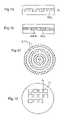
- FIG. 17illustrates an embodiment having concentric and alternating rings Z 1 and Z 2 .
- FIG. 18illustrates an embodiment having an array of regions Z 1 in an overall region
- FIG. 19is a diagrammatic view of the assembly of FIG. 4 after depositing a surface layer
- FIG. 20illustrates the assembly of FIG. 19 after molecular bonding of a final substrate
- FIG. 21illustrates the assembly of FIG. 20 during application of a lift-off operation
- FIG. 22is a diagrammatic view of a wafer obtained after lifting off of the assembly of FIG. 20 and subsequent polishing,
- FIG. 23is a view of a separable assembly of the embodiment illustrated in FIG. 4 .
- FIG. 24illustrates the assembly of FIG. 23 after production of some or all of the components, for example a first transistor gate,
- FIG. 25illustrates the assembly of FIG. 24 after deposition of oxide
- FIG. 26illustrates the assembly of FIG. 25 after planarization by CMP
- FIG. 27illustrates the assembly of FIG. 26 after molecular adhesion bonding (including heat treatment),
- FIG. 28illustrates a portion of the assembly of FIG. 27 after separation and deoxidization
- FIG. 29is a view of a separable assembly of the embodiment illustrated in FIG. 4 .
- FIG. 30illustrates the assembly of FIG. 29 after production of components
- FIG. 31illustrates the assembly of FIG. 30 after separation with no transfer to a target substrate, by hydrofluoric etching and/or application of mechanical forces,
- FIG. 32illustrates the assembly of FIG. 31 after separation into a final substrate and a substrate that can be recycled
- FIG. 33is an alternate embodiment of the assembly of FIG. 30 , after cutting of trenches or notches between components,
- FIG. 34illustrates the assembly of FIG. 33 showing a component in the process of being lifted off, for example after hydrofluoric etching,
- FIG. 35is a view of an assembly analogous to the assembly illustrated in FIG. 4 .
- FIG. 36illustrates the assembly of FIG. 35 after adhesive bonding of a transparent substrate
- FIG. 37is a view of the lower portion of the assembly illustrated in FIG. 36 after lifting off
- FIG. 36is a view of the upper portion of assembly illustrated in FIG. 37 after lifting off and polishing,
- FIG. 39is a view of an assembly analogous to that of FIG. 4 showing regions eliminated by chemical and mechanical cutting,
- FIG. 40illustrates the assembly of FIG. 39 after bonding an upper substrate
- FIG. 41is a view of a larger scale of an assembly including interleaved regions Z 1 and Z 2 ,
- FIG. 42is a view of an assembly analogous to that of FIG. 4 .
- FIG. 43illustrates the assembly of FIG. 42 after deposition of an epitaxial stack based on GaN
- FIG. 44illustrates the assembly of FIG. 43 after bonding a substrate
- FIG. 45illustrates the assembly of FIG. 44 at the time of lifting off
- FIG. 46is a view of the upper portion of the assembly illustrated in FIG. 45 after polishing
- FIG. 47illustrates the assembly of FIG. 45 after removal of the layer under the stack
- FIG. 48is a view of a substrate including a buried weak layer
- FIG. 49is a view of a substrate including a buried weak layer portion.
- Some embodiments of the method according to the inventiontend to encourage lifting of the layer off its substrate at the overall level, more specifically on the scale of the whole of the substrate, while others tend to delimit fragments.
- FIGS. 1 and 2An assembly to be produced in the former case is shown diagrammatically in FIGS. 1 and 2 , the interface or intermediate layer shown diagrammatically in FIG. 2 representing the region in which local bonding differences are to be created.
- FIG. 3in particular shows one example of the preparation of a surface intended to participate in an interface having, in accordance with the invention, two regions having different mechanical strengths.
- the objectis to obtain a central region Z 1 whose mechanical strength E c1 is less than that E c2 of a peripheral region.
- Z 2around the central region.
- FIG. 4shows the option in which the substrate 11 and the thin layer 14 are of monocrystalline silicon and two intermediate layers 12 and 13 are formed prior to bonding on the substrate 11 and the thin layer 14 , respectively.
- the two intermediate layers 12 or 13may suffice, and the situation in which neither of them exists (i.e. that of Si/Si bonding) must be considered (i.e. there are two special cases). If the intermediate layers 12 and 13 exist and are both of SiO 2 , the system is referred to as SiO 2 /SiO 2 bondinG. If only one of the two exists, and consists of SiO 2 , then the system is referred to as Si/SiO 2 bonding.
- the layer 14is referred to as the active layer, being the layer comprising the components, except for certain special cases in which an additional, for example epitaxial, layer is deposited onto the layer 14 .
- the thin layeris obtained by thinning the structure chemically and/or mechanically.
- BSOIbonded SOI
- BESOIbond and etch back SOI
- these variantsare based on physical removal of the original substrate by polishing techniques and/or chemical etching techniques.
- Other variants, partially described hereinbefore as layer transfer techniques,are based, in addition to molecular adhesion bonding, on separation by “cutting” or cleaving along a weakened region, such as the methods described in the documents U.S. Pat. No. 5,374,564 (or EP-A-533551) and U.S. Pat. No. 6,020,252 (or EP-A-807970): separation along an implanted region, or in the document EP 0925888: separation by fracture along a buried layer that has been rendered porous.
- a temporary maskcan first be used to deposit a protection layer, for example a layer of silicon nitride Si 3 N 4 , onto only the ring of the silicon oxide SiO 2 layer(s) 12 and/or 13 .
- the oxide layercan be prepared in several ways (deposition, thermal oxidation of the silicon) and can have a thickness that varies according to the application. For this example, a 1 ⁇ m thick thermal oxide is chosen. The following structure is therefore obtained: the surface of the central disc is formed of oxide only and the surface of the external ring (which is typically a few mm wide) is formed of the oxide covered with an additional protection layer (for example of nitride).
- hydrofluoric acid etchingto roughen the surface of the oxide, the roughening required increasing with the thickness of oxide removed.
- the roughnesscan be optimized, in particular as a function of the method of producing the components (or of epitaxial growth), which must be formed without delamination, and the method adopted for the final separation.
- hydrofluoric acid etching to remove a thickness of oxide of the order of a few hundred to a few thousand ⁇is a good starting compromise.
- a nitride thickness of the order of 1000 ⁇protects the underlying oxide from hydrofluoric acid etching, which increases the roughness of the central region of the oxide layer(s) 12 and/or 13 .
- the nitrideis subsequently removed by etching with hot (>110° C.) orthophosphoric acid (H 3 PO 4 ), for example.
- H 3 PO 4orthophosphoric acid
- Thiscan be combined with selective wet or dry cleaning to obtain different hydrophilic properties between the regions Z 1 and Z 2 .
- the resulting effectis one of weaker bonding than the standard bonding at the center and bonding identical to the standard bonding at the location of the ring.
- the oxide removedis thick, in particular because the application requires this (especially in the range of a few thousand ⁇ , knowing that 5000 ⁇ is a good starting compromise in many cases), it must be noted that in addition to the required effect of locally increased roughness, a difference in level is created between the central region (which has been hydrofluoric acid etched) and the ring (which has been protected from this etching). To obtain bonding of very high quality in the ring, in combination with bonding of satisfactory quality in the central region, it may be necessary to eliminate or reduce the difference in level in some cases. It can be appropriate to use polishing for this (for example chemical/mechanical polishing).
- polishingthat is a priori uniform results, through a planarizing effect that is well known to the person skilled in the art of microelectronics, in preferential polishing of the emergent region, i.e. the region of the ring in the present instance.
- the polishingcan also be intentionally localized to the rinG.
- the ringcan be preferentially polished by using a polishing cloth with a central opening, for example, thereby reducing the level of the ring to that of the central region that has been hydrofluoric acid etched.
- polishingleads to higher bonding energies than are obtained by conventional molecular adhesion bonding (with no polishing).
- An alternative to thisis to roughen all of the intermediate layer(s) 12 and/or 13 , more specifically without protecting the ring, but to add treatment localized to the ring that significantly increases the bonding strength.
- treatmentsinclude, for example, the use of an oxygen plasma or localized annealing, one aim of which would be, through a flow effect, to reconstruct and reduce the roughness of the surface of the oxide, or any other treatment known to the person skilled in the art to improve the cohesion of the assembly. These treatments have the advantage that they do not create any relief.
- Another alternativerelates to the use of localized thermal annealing (laser beam, non-uniform furnaces, heating by lamps, and the like) after the bonding operation.
- localized thermal annealinglaser beam, non-uniform furnaces, heating by lamps, and the like
- a 100° C. annealing temperature difference after bondingcan significantly vary the bonding energy, especially in the range of temperatures beyond 800° C.
- This alternativecan be used in combination with roughening at least one intermediate layer 12 or 13 , or alone (more specifically with no step of roughening everything).
- SiO 2 /SiO 2 bondingis to anneal the whole of the structure at 1000° C. and to heat the ring selectively to 1200° C. Another is not to anneal the whole of the ring at a temperature of 1000° C.
- the annealing temperaturecan be considered to be at a maximum at the edges of the substrate and to fall on approaching the center of the substrate.
- Another variant of the method of producing a separable substratecan be based on a difference in chemical nature between the region Z 1 and the region Z 2 .
- the following pairsmay be cited by way of non-exhaustive example: Z 1 ⁇ SiO 2 and Z 2 ⁇ Si; Z 1 ⁇ Si 3 N 4 and Z 2 ⁇ SiO 2 ; Z 1 ⁇ Si 3 N 4 and Z 2 ⁇ Si, and the like. Only the pair Z 1 ⁇ SiO 2 and Z 2 ⁇ Si is described here.
- a protective ring(of resin, deposited PECVD, and the like) a few mm wide is deposited onto a silicon substrate to define the dimensions of the region Z 2 .
- the structureis then etched (wet or dry, by any of the techniques conventionally employed to etch silicon) so that the etching attacks only the unprotected region.
- Mechanical attackmilling, polishing, and the like.
- the operation of depositing a protection layeris no longer indispensable.
- a silicon waferis obtained with a recess at the center, as shown in FIG. 6 .
- An oxideis deposited by the CVD process on the resulting substrate with a recess.
- the thickness of the layer of oxide depositedis much greater than the depth of the recess, producing the structure shown in FIG. 7 .
- Planarizing by polishingeliminates the difference in level between the ring and the center of the structure as well as the high inherent roughness of this type of deposit (see FIG. 8 ).
- Hydrofluoric acid etchingthen produces the structure shown in FIG. 9 .
- hydrofluoric acid etchingis stopped when the silicon is flush with the rinG. This produces a “silicon ring and roughened oxide at the center” configuration, which defines an energy difference between the regions Z 1 and Z 2 , firstly because these two regions have different roughnesses and secondly because the nature of the material is different (different molecular adhesion bonding properties).
- the above sequencecan be modified to yield a “silicon ring and non-roughened oxide at the center” configuration.
- the hydrofluoric acid etching stepcan be eliminated, for example, and the previous polishing step extended so that polishing the silicon ring results in a flush surface.
- the energy difference between the regions Z 1 and Z 2is essentially caused by the difference in the nature of the materials. In this case, the difference is smaller.
- a recess and an oxide deposithave been cited in the situation where they are produced on the substrate 11 (with the result that the FIG. 10 configuration is obtained after bonding).
- a variantconsists in carrying out these operations on the side of the thin layer 14 (see FIG. 12 ), or even on both sides (see FIG. 11 ).
- Methods for other pairs of materials that can exhibit a difference in mechanical strengthcan include a small number of additional steps. For example, if the aim is to obtain the pair Z 1 ⁇ Si 3 N 4 and Z 2 ⁇ SiO 2 , Si 3 N 4 must be deposited in addition to the oxide, taking care to define the required ring for the whole of the structure using conventional masking techniques (photolithography, mechanical methods, and the like).
- This structurehas the advantage of excellent chemical etching (for example hydrofluoric acid etching) selectivity between the two materials concerned, which could facilitate separation through easy and selective removal of the ring by chemical etching.
- FIG. 13is a variant of FIG. 11 in which the central layer does not have the same dimensions in the substrate and in the thin layer,
- FIG. 14shows an assembly in which the interface layer between the substrate and the thin layer has a central portion Z 1 of a material (Si 3 N 4 ) different from that (SiO 2 ) of the peripheral portion Z 2 , these two portions being of different materials (here Si) than the substrate and the thin layer,
- FIG. 15is a variant of FIG. 10 in which there is a plurality of regions Z 1 of a material different from that of the support,
- FIG. 16is a variant of FIG. 14 in which there is a plurality of regions Z 1 and a plurality of regions Z 2 of materials (here Si 3 N 4 and SiO 2 ) different from those (here Si) of the substrate and the thin layer.
- FIGS. 15 and 16can correspond to a plurality of geometries of which FIGS. 17 and 18 are examples (at the die level or otherwise):
- FIG. 17shows a configuration with a plurality of concentric bands Z 1 or Z 2 .
- FIG. 18shows a configuration having an array (made up of rows and columns) of regions of one type (here Z 1 ) in an overall region of the other type (Z 2 ).
- the benefit of the separable substratedepending on the thickness of the unprocessed active layer or of the processed active layer (i.e. its thickness when it has been processed to produce all or part of a component), is that it allows separation of the active layer to obtain either a self-supporting layer (a relatively thick layer, whether the thickness is already present in the separable substrate as manufactured or obtained during deposition steps subsequent to its fabrication, as is the case in an epitaxial growth step) or a surface layer, which is generally thinner, transferred onto a target support, whether the latter is the final support or merely a temporary support which is itself intended to be detached.
- a self-supporting layera relatively thick layer, whether the thickness is already present in the separable substrate as manufactured or obtained during deposition steps subsequent to its fabrication, as is the case in an epitaxial growth step
- a surface layerwhich is generally thinner, transferred onto a target support, whether the latter is the final support or merely a temporary support which is itself intended to be detached.
- transfercan be effected by molecular adhesion bonding of what is to become the thin layer to be transferred to another substrate.
- a separation methodis described next in the context of producing a new SOI structure that is referred to herein as the second SOI structure.
- This kind of methoda priori less direct than the techniques previously mentioned, nevertheless has a number of benefits.
- the example chosen hererelates to the production of a second SOI substrate with a buried oxide layer 500 ⁇ thick, which thickness is difficult to obtain using this kind of method directly.
- the first structureis obtained by one of the methods previously described, yielding a separable substrate corresponding to FIG. 4 .
- the monocrystalline silicon layer 14is to become the active layer.
- this separable substratein which the central region of the connecting layer has been roughened before bonding and has not undergone any strengthening heat treatment at very high temperatures (preferably less than 1000° C. and even better less than 1000° C. or even 900° C.), a 500 ⁇ oxide layer is formed by thermal oxidation to yield the structure shown in FIG. 20 . This oxide is to become the buried oxide of the second SOI structure.
- the separable substrate( 11 + 12 + 13 + 14 + 15 ) is molecular adhesion bonded to a silicon substrate 16 that is to become the final support of the active layer (see FIG. 2 ).
- the stack obtainedis preferably stabilized at a high temperature (1000° C.) to consolidate strongly the second bond at the interface of the layers 15 and 16 .
- This second bondis conventional in the sense that there is no differentiation between regions of different mechanical strength.
- the first bondif subjected to the same treatment, nevertheless has, at least in its central portion, corresponding to the region Z 1 , a mechanical strength less than that of the second bond.
- a chemical and/or mechanical separation methodcan be used.
- the stack obtained as aboveis first immersed in a hydrofluoric acid bath, one object of which is to overetch the oxide layers 12 and 13 , starting from the edges of the assembly, to eliminate the ring corresponding to the region Z 2 and reach the region Z 1 .
- the two interfaces 12 / 13 and 15 / 16are preferentially etched.
- the interface 12 / 13 of the separable substrateis advantageously an oxide/oxide interface. It therefore yields more readily than the interface 15 / 16 between the oxide and the silicon. Accordingly, during this step of lifting off the ring of higher mechanical strength, there is less surface etching at the interface of the second bond than at the interface of the separable substrate.
- the acidreaches the low energy region (the central region, see FIG.
- the 500 ⁇ thick buried oxide layer 15 formed previously on the layer 14could have been formed on the substrate 16 before bonding rather than on the layer 14 .
- Another variantdivides the 500 ⁇ thickness into two portions, with one portion on the substrate 16 , for example 250 ⁇ thick, and the other portion on the layer 14 , also 250 ⁇ thick in this example.
- the two molecular adhesion bonded interfacesare both of the oxide/oxide type, stabilization of the second bond at high temperature can be carried out in such a way as to guarantee that preferential hydrofluoric acid etching occurs at the first interface.
- the creation of a mechanically weak region Z 1achieves preferential separation of the complete stack at the first bond interface, and the region Z 2 firstly yields an active layer 14 of good quality and secondly prevents the onset of cracks that can cause losses of yield and a reduction in the surface of the active film caused by peeling of the film at the edge, and thus a strong increase in particulate contamination of the wafers.
- the first operations relating to the fabrication of the transistorsessentially consist in producing the first CMOS transistor gate (see FIG. 24 ) on a separable substrate using conventional technology (see FIG. 23 ), as shown in FIG. 4 , for example, in exactly the same way as previously described for the production of SOI structures with a thin buried oxide layer.
- the bonding stabilization temperaturecan be reduced in a temperature range of the order of 900° C. to 1000° C.
- An oxide layer with a thickness of the order of 1 ⁇ mis then deposited onto this substrate (see FIG. 25 ) using a conventional deposition technique (for example CVD).
- the oxideis planarized using a conventional chemical/mechanical polishing technique (see FIG. 26 ). This is followed by molecular adhesion bonding to another silicon substrate 16 (see FIG. 27 ). The bonding is preferentially stabilized at a temperature from 1000° C. to 1100° C. if the structures formed for the first gate can withstand this high a temperature, or at temperatures of the order of 900° C. to 1000° C. otherwise. Finally (see FIG. 28 ), separation is carried out in exactly the same way as previously (insertion of a blade, pressurized water jet, compressed air jet, etc.). Before resuming the transistor fabrication process, in particular to produce the second gate (on the new “substrate” shown in FIG.
- the remainder of the oxide layer 13is removed by chemical etchinG. Because the oxide is etched with a hydrofluoric acid solution of known etching selectivity with respect to silicon, etching stops naturally once the oxide has been entirely etched, revealing a silicon surface.
- the major advantage of this technique over other fracture techniques, for example obtained by way of implantation,is that it does not necessitate excessively complex finishing sequences that are problematic in terms of their potential to create defects, as for a final polishing operation, for example.
- the remainder of the double-gate transistor fabrication processwill be obvious to the person skilled in the art.
- the same processcan be used in many other applications. If the first SOI structure (see FIG. 4 ) is used to produce transistors, circuits, components, and the like, these can be finally transferred onto many types of dedicated support.
- the substrate 16can be chosen for its electrical insulation properties (high-resistivity silicon, quartz, sapphire, and the like) to provide an ideal support for microwave and telecommunication circuits, thereby limiting losses in the substrate.
- a transparent substrateis chosen for the final support.
- FIGS. 29 to 32Another example of separation is briefly described here (see FIGS. 29 to 32 ) in the case of producing circuits on thin substrates.
- the final thicknesses of interestare typically less than a few hundred ⁇ m, even of the order of a few tens of ⁇ m. They relate, for example, to power applications or applications to smart cards and other circuits for which some flexibility is required (plastics material supports, curved supports, and the like).
- One variantrelates to a type of separation necessitating no transfer to a target substrate.
- the objectis to achieve separation without transferring the layer 14 after producing the circuits or components C, when the layer 14 is sufficiently thick to be self-supporting but too thin to withstand without damage a circuit production process (typically less than a few hundred ⁇ m thick, and even of the order of a few tens of ⁇ m).
- the method of producing the separable substrateis identical in every respect to any of those described previously to produce the FIG. 4 structure, for example.
- This 645 ⁇ m thick substrateis then molecular adhesion bonded, for example, to a 725 ⁇ m wafer, forming areas of lower mechanical strength.
- the 725 ⁇ m waferis then thinned to the required thickness of 80 ⁇ m, for example by planning and chemical/mechanical polishing.
- the resulting assemblytherefore corresponds to the standards and offers sufficient resistance to the processes for fabricating some or all of the components.
- one of the separation techniques previously citedmay be used (see FIG. 31 , hydrofluoric acid etching and mechanical stresses), except that the substrate 16 can be omitted. Its presence can be beneficial in some cases, however.
- the self-supporting layer 14alone represents the final substrate of interest, characterized by a substrate thickness of 80 ⁇ m, including the components. The remainder of the substrate can be recycled.
- FIG. 33shows cuts between the components, extending to just below the future separation region
- FIG. 34shows a pull-off support SA bonded to one of the fragments and adapted to allow pulling off after hydrofluoric acid etching, if any.
- the weakening parametershave to be adapted to the technological operations that have to be carried out on the separable substrate prior to separation, in particular thermal and chemical treatments, and according to the nature of the mechanical stresses.
- the separable substrateconsists of a surface layer of germanium having an SiO 2 —SiO 2 bonding interface that has to withstand an epitaxial growth temperature of 550° C. (which is typical in the case of growing GaInAs to constitute a solar cell for use in space), then the rms roughness must advantageously be 0.4 nm for the substrate to be separable.
- a monocrystalline silicon support whose thickness is greater than around 50 ⁇ mis too fragile in this context, because its thickness is too high if it is subjected to a bending force, as can happen regularly with a smart card.
- FIG. 35shows a starting assembly similar to that shown in FIG. 4 , with a starting substrate 11 ′ covered with a layer 12 ′ of silicon oxide that is molecular adhesion bonded to a second layer 13 ′ of silicon oxide, in turn covered with a silicon layer 14 ′.
- the circuitsare produced within the silicon layer 14 ′.
- an adhesiveis preferably chosen that produces a very thin layer 15 ′, whilst having the highest possible mechanical strength at low temperature, for example less than 400° C., so as not to risk damaging the components of the active layer produced after this bonding step.
- Thesecan advantageously be adhesives hardened by heat or by exposure to UV radiation (in this latter case, it is sufficient to choose a final substrate 16 ′ that is transparent to UV).
- the ringApart from limited chemical etching of the ring, it is further possible to eliminate the ring by making a circular cut in the structure after adhesive bonding.
- the cuttingcan advantageously be effected by a laser at the boundary between the high bonding energy region and the low bonding energy region. If the ring is only a few mm wide, or even narrower, it is then possible to reuse the substrate.
- the residue of the first substrateis obtained, the support of the substrate referred to until now as “separable” (see FIG. 37 ) and reusable, preferably after polishing the layer 12 ′ and the active layer 14 ′ ( FIG. 38 ) that is transferred onto the other support 16 ′ or alternatively is free and self-supporting if the thickness of the layer 14 ′ is appropriate.
- the second substrate 16 ′can instead be merely an intermediate substrate in a much longer process that will continue either with the pure and simple elimination of the intermediate substrate 16 ′ or another layer transfer operation onto a yet further support, generally involving elimination of the substrate 16 ′.
- the separable substrate obtained with the aid of the technique previously describedis bonded to the intermediate substrate after it has been “processed”.
- the intermediate substratecan be rigid or flexible (see the above examples). If it is rigid, it can even be a silicon wafer.
- adhesive filmsknown to the person skilled in the art can be envisaged for the adhesive bonding, in particular for the operations of cutting silicon wafers and encapsulating integrated circuits or packaging or back-ending (“Blu Tak”, Teflon® adhesive film, and the like). If the adhesive film is double-sided, it may be as well to stick an intermediate substrate to the rear face of the film, to act as a substrate or support for stiffening the assembly at cutting time.
- the lift-off techniquesinclude the application of traction and/or shear and/or bending forces. It may be as well to combine the application of force with chemical etching of the interface, or other means, such as ultrasound. If the interface to be lifted off is of the oxide type, etching the low energy interface makes it easier for the bonding interface to yield and therefore facilitates the transfer of the processed layer to the intermediate substrate. Under these conditions, it is advantageous for the processed layers to be protected (for example by an additional deposit of nitride in the case of hydrofluoric acid etching).
- Stressescan be applied directly to the thin film or to the intermediate substrate (known as a handle). They can be mechanical stresses (in particular applied by inserting a blade at the bonding interface), and/or use a lift-off tool (see WO 00/26000), and/or a jet, or involve inserting a gas flow, as described in the document FR 2796491, and/or a liquid (see EP 0925888, EP 0989593).
- a gas flowor even a liquid flow, for example a flow of hydrofluoric acid if the interface is of oxide
- the separable substratecan advantageously be prepared beforehand (for example by chemical etching) to feed the fluid locally to the bonding interface.
- the intermediate substratewhich is sometimes referred to as a “handle”
- the intermediate substratecan then be cut, totally or in part (to form notches or cutting precursors), into elements corresponding to the electronic components, which can be transferred to different supports.
- the transfercan be collective, in which case all of the components, even if they are interconnected only by a support, are transferred at the same time in the same technological operation, or component by component (or die by die), if the latter are transferred one after the other.
- the supportscan be of plastics material, as in the case of a smart card, and in this case an adhesive is advantageously used for the transfer.
- the elementscan also be transferred onto a wafer incorporating other electronic or opto-electronic devices, in which case the transfer can again use a molecular adhesion technique (see FIGS. 4 and 19 to 22 , imagining the additional presence of components formed in the layer 14 ).
- the elementscan be transferred by conventional means such as pick and place means.
- the elementscan also be transferred onto another support to improve the thermal properties, for example.
- the thin layer, previously bonded to its final supportcan be separated (element by element, or globally) from its handle by means of mechanical forces.
- the regions Z 1 and Z 2may not define a system comprising a central circular region Z 1 surrounded by an outer ring Z 2 .
- a multitude of other structurescan be envisaged.
- the array of squares in FIG. 18can be replaced by arrays of other shapes (rows, columns, concentric circles, and the like) whose pitch and other geometrical dimensions can vary as a function of the application and the separation technique employed.
- the benefit of adopting an arraymay prove to be preferable if the structure to be produced imposes high mechanical stresses that are transmitted to the connecting interface (in this case short-range repetition of areas of good mechanical strength is preferable), or if the layer 14 may feature holes, whether intentional or otherwise, locally uncovering the connecting region, which may in turn be subject to untimely delamination whose epicenter is the hole, or to simplify the method (for example for cutting into individual dies) in the case of producing dies.
- dimensions of the order of 1 ⁇ mare preferred for structures having to withstand high stresses (for example hetero-epitaxy or any other deposition or technological step applying significant tension or compression to the structure), or in the case of small circuits, or of circuits produced with submicron photolithographic resolution.
- scales of the order of 1 mm or even 1 cmare preferable.
- Many combinations of more than two regionscan of course be envisaged (Z 1 ; Z 2 , Z 3 , and so on).
- a continuum of regions characterized by a continuous variation of the mechanical strengthcan be envisaged.
- the mechanical strength decreasing continuously from a maximum value in the vicinity of the edge to a minimum value at its centercan be envisaged.
- the variationcan optionally be circularly symmetrical about an axis perpendicular to the plane of the substrate.
- Production processes yielding this type of substrate and their use in separationare in all respects similar to those described with reference to FIGS. 1 to 8 , provided that the geometrical shapes employed are suitable (mask shapes for formation of protection layers for selective roughness, mask shapes for selective deposition, shape of polishing tissues for preferentially polishing eccentric rings, and the like).
- the above geometrical shapesare compatible with the transfer of a layer 14 as a whole from the separable original substrate 11 + 12 + 13 + 14 to the target substrate 16 .
- FIG. 41shows one example of this, with enlargement of the region that subsequently accommodates the die (or any other component).
- This structurecan be repeated as many times as there are components to be separated on the original substrate.
- each region Z 2surrounds or simply extends along the contour of each fragment of the region Z 1 .
- the surface area of the componentcan correspond exactly to the region Z 1 , or be greater than or less than the latter, in configurations where one of the surfaces of the component and of the region Z 1 encompasses the other.
- the configuration adopteddepends on the separation technique to be used, which can be the same as those previously described for separating a substrate having only a ring Z 2 around a central disc Z 1 .
- One interesting variantconsists in using conventional component cutting techniques (sawing, laser cutting, and the like) to cut or delimit trenches, at least partially around dies, fragments, and the like.
- Another beneficial variantis based on the use of chemical etching associated with a photolithography operation to produce identical trenches and/or to remove the connecting region corresponding to the region Z 2 .
- FIG. 41shows in the case of one particular example, the vertical dashed lines indicate the contour of the required fragments. For example, after preparing molecular adhesion bonding over a large area, only layers 3 and 4 are cut to the contour shown, after which each fragment is lifted off the substrate 1 , which amounts to considering that the substrate is lifted off each fragment (as an alternative, all the layers or all of the fragments can be cut at one and the same time).
- the risk of delamination during treatment stepsfor example to produce electronic, optical or other components on the layers 3 or 4 , is reduced, whereas, when lifting off is required, it propagates without difficulty, in a controlled manner, in the central region (it may have been initiated at the periphery).
- the embodiments previously describedare not limited to the single case of monocrystalline silicon, and can be extended to many materials, such as other semiconductor materials (Ge, SiGe, SiC, GaN and other equivalent nitrides, AsGaInP, and the like), ferro-electric and piezo-electric materials (LiNbO 3 , LiTaO 3 ), and “treated” magnetic materials, whether components are produced before separation or not.
- other semiconductor materialsGe, SiGe, SiC, GaN and other equivalent nitrides, AsGaInP, and the like
- ferro-electric and piezo-electric materialsLiNbO 3 , LiTaO 3
- “treated” magnetic materialswhether components are produced before separation or not.
- the root mean square (rms) roughnessshould advantageously be 0.4 nm for the substrate to be separable.
- Another exampleis that of epitaxially growing an epitaxial stack on a separable substrate.
- the epitaxial stack concernedis based on composite semiconductors derived from GaN (AlN, GaAlN, GaAlInN, and the like).
- One methodconsists of using one of the processes previously described to form a separable structure equivalent to that of FIG. 4 (or FIG. 26 or FIG.
- the layer 14is of SiC (the transferred Si face is at the top in the figures)
- the layers 12 and 13are of silicon oxide, as in the FIG. 4 example
- the substrate 11is of polycrystalline SiC (or sapphire).
- the stack 15 ′′ based on nitrides( FIG. 43 ) is grown epitaxially on this structure (FIG. 42 ).
- the epitaxial techniques usedcan be those well known to the person skilled in the art such as molecular beam epitaxy (MBE) for one category, and metallo-organic chemical vapor deposition (MOCVD) for another category. In the former case, the epitaxial growth temperatures rarely exceed 600° C., whereas the typical temperatures for the second category are of the order of 1050° C.
- the choice of the pairs or sets of regions Z 1 , Z 2 , etc.must be optimized.
- one of the processes previously described based on roughening of the two oxide layers 12 and 13 by hydrofluoric acid etchingis chosen, for example, and another variant consists in forming a 5 mm wide ring from the edge of the substrate.
- Subsequent MOCVD epitaxial growth at 1100° C.produces a stack whose thickness is of the order of 1 ⁇ m.
- the structureis optionally annealed before the epitaxial growth stage, typically in the temperature range from 900° C. to 1200° C., in order to consolidate strongly the mechanical strength of the ring.
- the assemblyis subjected to deposition of oxide, planarization by CMP, molecular adhesion bonding (for example onto a silicon substrate), and annealing at 1100° C. to strength this latter bonding. and the layer 16 is produced ( FIG. 44 ). Finally, there is separation at the bonding interface ( FIG. 45 ). A few hours in a 50% hydrofluoric acid bath are sufficient to etch the oxide layer laterally to a depth of a few mm where this interface corresponds to the region Z 2 , thereby uncovering the region Z 1 . This is followed by separation by means of mechanical forces, for example by inserting a blade (not shown), applying a pressurized water jet, or applying a compressed air jet, using the techniques previously described, for example.
- a final deoxidation stepremoves the residue of the oxide layer 13 ( FIG. 46 ).
- the SiC layer 14 that served as a nucleation layer for the epitaxial stackcan optionally be eliminated by etching ( FIG. 47 ).
- Diodescan be produced before or after the final transfer.
- the interface between the substrate and what is to form the “active” layercan instead take the form of a buried weak layer, formed of microcavities, microbubbles, or platelets, for example. This process can be used with many semiconductor and other materials.
- the difference between regions with different mechanical strengthsis obtained by different levels of weakening; in the case where, as in FIGS. 1 to 3 , a central region is required to be surrounded by a peripheral region of greater mechanical strength, it is sufficient to weaken the structure less at the periphery than at the center, for example, by introducing at the periphery smaller amounts of the substances for weakening the region (for example by hydrogen implantation); this can be obtained by masking a portion of the layer during a portion of the implantation operation, for example, or by modifying the sweep during implantation; it can also be achieved by carrying out successive implantations, under different conditions, in the various regions whose properties are to be different. Regions can also be weakened differently by applying different heat treatments to them to obtain different levels of weakening.
- a porous layercan be obtained from the following materials in particular: Si, GaAs, InP, GaAsP, GaAlAs, InAs, AlGaSb, ZnS, CdTe and SiGe, in monocrystalline, polycrystalline or amorphous forms.
- porous siliconby electrolysis in hydrofluoric acid.
- the person skilled in the artknows how to vary the porosity of the Si by modifying the concentration of the hydrofluoric acid or by varying the current. For example, reducing the hydrofluoric acid concentration from 50% to 20% changes the porosity from 2.1 g/cm 3 to 0.6 g/cm 3 .
- a monocrystalline layer of Siis then produced on this porous layer by epitaxial growth (see FIG. 48 , which represents a structure comprising a substrate 21 , the porous layer 22 , having controlled differences in porosity between the regions Z 1 ′ and Z 2 ′, and a thin layer 23 ).
- Smoothing annealing of the hydrogen annealing typeis advantageously employed before the epitaxial growth step to stop up the surface of the pores at least in part.
- This monocrystalline layerwhich thus becomes the active layer, depends on the intended applications.
- the active layerafter separation it can become a self-supporting layer (if it is relatively thick) or it can be transferred to a target substrate (for example by molecular adhesion), especially if the layer is thin.
- the active layercan be lifted off its substrate by chemical means or by introducing a fluid locally into the porous layer.
- the interfacecan be a simple contact surface or a connecting layer
- the fragmentscan be distributed in a network of squares, lines, concentric circles, etc.,
- the geometrical definition of the fragmentsis preferably related to the location and the size of the dies (to the nearest region Z 2 or the nearest sawing line),
- the surface preparation step before bondingcan include roughening of the oxide layer
- the preparation before bondingcan affect the roughness but also the hydrophilic properties
- both regionscan be roughened and the roughness of only the second region reduced
- the difference between Z 1 , Z 2can result from heat treatment after localized molecular bonding; alternatively, localized thermal annealing can be used after the bonding operation (laser beam, non-uniform furnace, heating by lamps, and the like),
- the latterwhen the interface is a buried layer weakened by implanting a gaseous element, the latter preferably remains gaseous
- portions of material corresponding to the region Z 2can advantageously be eliminated by chemical etching and/or by mechanical removal of material (machining),
- the lift-off stepcan be effected by etching in a vacuum and/or application of stresses; a jet of water, air or pressurized fluid can be used,
- regions Z 3 , and even Z 4there can be regions Z 3 , and even Z 4 , having levels of mechanical strength different from those of the regions Z 1 and Z 2 ,
- the difference in mechanical strength between the regionscan result from a difference of composition (interface formed of a layer with one region of one material and the other region of another material, or an interface formed in part by the material of the substrate or the layer and in part by a transferred layer).
Landscapes
- Engineering & Computer Science (AREA)
- Microelectronics & Electronic Packaging (AREA)
- Condensed Matter Physics & Semiconductors (AREA)
- General Physics & Mathematics (AREA)
- Manufacturing & Machinery (AREA)
- Computer Hardware Design (AREA)
- Physics & Mathematics (AREA)
- Power Engineering (AREA)
- Recrystallisation Techniques (AREA)
- Element Separation (AREA)
- Mechanical Treatment Of Semiconductor (AREA)
- Weting (AREA)
- Laminated Bodies (AREA)
- Materials For Medical Uses (AREA)
Abstract
Description
Claims (18)
Applications Claiming Priority (4)
| Application Number | Priority Date | Filing Date | Title |
|---|---|---|---|
| FR0105129 | 2001-04-13 | ||
| FR01/05129 | 2001-04-13 | ||
| FR0105129AFR2823596B1 (en) | 2001-04-13 | 2001-04-13 | SUBSTRATE OR DISMOUNTABLE STRUCTURE AND METHOD OF MAKING SAME |
| PCT/FR2002/001266WO2002084721A2 (en) | 2001-04-13 | 2002-04-11 | Detachable substrate or detachable structure and method for the production thereof |
Publications (2)
| Publication Number | Publication Date |
|---|---|
| US20050029224A1 US20050029224A1 (en) | 2005-02-10 |
| US7713369B2true US7713369B2 (en) | 2010-05-11 |
Family
ID=8862351
Family Applications (1)
| Application Number | Title | Priority Date | Filing Date |
|---|---|---|---|
| US10/468,223Expired - LifetimeUS7713369B2 (en) | 2001-04-13 | 2002-04-11 | Detachable substrate or detachable structure and method for the production thereof |
Country Status (9)
| Country | Link |
|---|---|
| US (1) | US7713369B2 (en) |
| EP (1) | EP1378003B1 (en) |
| JP (2) | JP4540933B2 (en) |
| KR (1) | KR100933897B1 (en) |
| CN (1) | CN100355025C (en) |
| AU (1) | AU2002304525A1 (en) |
| FR (1) | FR2823596B1 (en) |
| TW (1) | TW577102B (en) |
| WO (1) | WO2002084721A2 (en) |
Cited By (27)
| Publication number | Priority date | Publication date | Assignee | Title |
|---|---|---|---|---|
| US20060252229A1 (en)* | 2003-06-24 | 2006-11-09 | Jean-Pierre Joly | Integrated circuit on high performance chip |
| US20070281445A1 (en)* | 2003-10-28 | 2007-12-06 | Nguyet-Phuong Nguyen | Method for Self-Supported Transfer of a Fine Layer by Pulsation after Implantation or Co-Implantation |
| US20080038564A1 (en)* | 2003-09-30 | 2008-02-14 | Michel Bruel | Method of Producing a Plate-Shaped Structure, in Particular, From Silicon, Use of Said Method and Plate-Shaped Structure Thus Produced, in Particular From Silicon |
| US20080128868A1 (en)* | 2004-12-24 | 2008-06-05 | Tracit Technologies | Method of Transferring a Circuit Onto a Ground Plane |
| US20080237780A1 (en)* | 2007-03-26 | 2008-10-02 | Semiconductor Energy Laboratory Co., Ltd. | SOI substrate and method for manufacturing SOI substrate |
| US20080254591A1 (en)* | 2005-09-28 | 2008-10-16 | Chrystel Deguet | Method for Making a Thin-Film Element |
| US20080254596A1 (en)* | 2004-06-02 | 2008-10-16 | Tracit Technologies | Method for Transferring Wafers |
| US20090218560A1 (en)* | 2008-01-24 | 2009-09-03 | Brewer Science Inc. | Method for reversibly mounting a device wafer to a carrier substrate |
| US20100167499A1 (en)* | 2002-12-09 | 2010-07-01 | Commissariat A L'energie Atomique | Method for making a stressed structure designed to be dissociated |
| US20110092051A1 (en)* | 1997-12-30 | 2011-04-21 | Commissariat A L'energie Atomique | Process for the transfer of a thin film comprising an inclusion creation step |
| US8101503B2 (en) | 1996-05-15 | 2012-01-24 | Commissariat A L'energie Atomique | Method of producing a thin layer of semiconductor material |
| US8252663B2 (en) | 2009-06-18 | 2012-08-28 | Commissariat A L'energie Atomique Et Aux Energies Alternatives | Method of transferring a thin layer onto a target substrate having a coefficient of thermal expansion different from that of the thin layer |
| US8475693B2 (en) | 2003-09-30 | 2013-07-02 | Soitec | Methods of making substrate structures having a weakened intermediate layer |
| WO2014026292A1 (en)* | 2012-08-15 | 2014-02-20 | Mcmaster University | Arbitrarily thin ultra smooth film with built-in separation ability and method of forming the same |
| WO2014037792A2 (en) | 2012-09-07 | 2014-03-13 | Soitec | Method for separating at least two substrates along a selected interface |
| US8778775B2 (en) | 2006-12-19 | 2014-07-15 | Commissariat A L'energie Atomique | Method for preparing thin GaN layers by implantation and recycling of a starting substrate |
| US20140235032A1 (en)* | 2011-10-17 | 2014-08-21 | Shin-Etsu Chemical Co., Ltd. | Method for producing transparent soi wafer |
| US8852391B2 (en) | 2010-06-21 | 2014-10-07 | Brewer Science Inc. | Method and apparatus for removing a reversibly mounted device wafer from a carrier substrate |
| US9028628B2 (en) | 2013-03-14 | 2015-05-12 | International Business Machines Corporation | Wafer-to-wafer oxide fusion bonding |
| US9058974B2 (en) | 2013-06-03 | 2015-06-16 | International Business Machines Corporation | Distorting donor wafer to corresponding distortion of host wafer |
| US20150214098A1 (en)* | 2012-09-07 | 2015-07-30 | Soitec | Processing for fabrication of a structure with a view to a subsequent sepration |
| US9224630B2 (en) | 2010-03-31 | 2015-12-29 | Ev Group E. Thallner Gmbh | Method for producing a wafer provided with chips |
| US9263314B2 (en) | 2010-08-06 | 2016-02-16 | Brewer Science Inc. | Multiple bonding layers for thin-wafer handling |
| US9481566B2 (en) | 2012-07-31 | 2016-11-01 | Soitec | Methods of forming semiconductor structures including MEMS devices and integrated circuits on opposing sides of substrates, and related structures and devices |
| US20180096848A1 (en)* | 2014-01-23 | 2018-04-05 | Arizona Board Of Regents, Acting For And On Behalf Of Arizona State University | Method of providing an electronic device and electronic device thereof |
| US20180102272A1 (en)* | 2014-01-23 | 2018-04-12 | Arizona Board Of Regents, Acting For And On Behalf Of Arizona State University | Method of providing an electronic device and electronic device thereof |
| US10438884B2 (en) | 2017-11-28 | 2019-10-08 | Samsung Electronics Co., Ltd. | Carrier substrate and method of manufacturing semiconductor package using the same |
Families Citing this family (93)
| Publication number | Priority date | Publication date | Assignee | Title |
|---|---|---|---|---|
| FR2823599B1 (en)* | 2001-04-13 | 2004-12-17 | Commissariat Energie Atomique | DEMOMTABLE SUBSTRATE WITH CONTROLLED MECHANICAL HOLDING AND METHOD OF MAKING |
| FR2823596B1 (en) | 2001-04-13 | 2004-08-20 | Commissariat Energie Atomique | SUBSTRATE OR DISMOUNTABLE STRUCTURE AND METHOD OF MAKING SAME |
| FR2846788B1 (en) | 2002-10-30 | 2005-06-17 | PROCESS FOR PRODUCING DETACHABLE SUBSTRATES | |
| FR2847077B1 (en) | 2002-11-12 | 2006-02-17 | Soitec Silicon On Insulator | SEMICONDUCTOR COMPONENTS, PARTICULARLY OF THE MIXED SOI TYPE, AND METHOD OF MAKING SAME |
| FR2892228B1 (en)* | 2005-10-18 | 2008-01-25 | Soitec Silicon On Insulator | METHOD FOR RECYCLING AN EPITAXY DONOR PLATE |
| US20090325362A1 (en)* | 2003-01-07 | 2009-12-31 | Nabil Chhaimi | Method of recycling an epitaxied donor wafer |
| EP1437426A1 (en)* | 2003-01-10 | 2004-07-14 | Siemens Aktiengesellschaft | Process for producing single crystal structures |
| US6759277B1 (en)* | 2003-02-27 | 2004-07-06 | Sharp Laboratories Of America, Inc. | Crystalline silicon die array and method for assembling crystalline silicon sheets onto substrates |
| US7122095B2 (en) | 2003-03-14 | 2006-10-17 | S.O.I.Tec Silicon On Insulator Technologies S.A. | Methods for forming an assembly for transfer of a useful layer |
| FR2852445B1 (en)* | 2003-03-14 | 2005-05-20 | Soitec Silicon On Insulator | PROCESS FOR PRODUCING SUBSTRATES OR COMPONENTS ON SUBSTRATES WITH USEFUL LAYER TRANSFER FOR MICROELECTRONICS, OPTOELECTRONICS OR OPTICS |
| JP4794810B2 (en)* | 2003-03-20 | 2011-10-19 | シャープ株式会社 | Manufacturing method of semiconductor device |
| JP4581349B2 (en)* | 2003-08-29 | 2010-11-17 | 株式会社Sumco | Manufacturing method of bonded SOI wafer |
| JP4809600B2 (en)* | 2003-10-28 | 2011-11-09 | 株式会社半導体エネルギー研究所 | Method for manufacturing semiconductor device |
| JP4838504B2 (en)* | 2004-09-08 | 2011-12-14 | キヤノン株式会社 | Manufacturing method of semiconductor device |
| FR2876220B1 (en)* | 2004-10-06 | 2007-09-28 | Commissariat Energie Atomique | METHOD FOR PRODUCING MIXED STACKED STRUCTURES, VARIOUS INSULATING AREAS AND / OR LOCALIZED VERTICAL ELECTRICAL CONDUCTION ZONES. |
| US7405108B2 (en)* | 2004-11-20 | 2008-07-29 | International Business Machines Corporation | Methods for forming co-planar wafer-scale chip packages |
| FR2878648B1 (en)* | 2004-11-30 | 2007-02-02 | Commissariat Energie Atomique | RECTANGULAR SEMICONDUCTOR SUPPORT FOR MICROELECTRONICS AND METHOD OF MAKING SUCH A SUPPORT |
| JP2006216891A (en)* | 2005-02-07 | 2006-08-17 | Tokyo Univ Of Agriculture & Technology | Thin film element structure fabrication method and functional substrate for thin film element structure fabrication |
| JPWO2006118033A1 (en)* | 2005-04-27 | 2008-12-18 | リンテック株式会社 | Sheet-like underfill material and method for manufacturing semiconductor device |
| FR2888400B1 (en)* | 2005-07-08 | 2007-10-19 | Soitec Silicon On Insulator | LAYER TAKING METHOD |
| FR2889887B1 (en)* | 2005-08-16 | 2007-11-09 | Commissariat Energie Atomique | METHOD FOR DEFERING A THIN LAYER ON A SUPPORT |
| EP1777735A3 (en)* | 2005-10-18 | 2009-08-19 | S.O.I.Tec Silicon on Insulator Technologies | Recycling process of an epitaxial donor wafer |
| FR2893750B1 (en)* | 2005-11-22 | 2008-03-14 | Commissariat Energie Atomique | METHOD FOR MANUFACTURING SCREEN TYPE FLEXIBLE ELECTRONIC DEVICE COMPRISING A PLURALITY OF THIN FILM COMPONENTS |
| TWI285424B (en)* | 2005-12-22 | 2007-08-11 | Princo Corp | Substrate including a multi-layer interconnection structure, methods of manufacturing and recycling the same, method of packaging electronic devices by using the same, and method of manufacturing an interconnection device |
| US7829436B2 (en) | 2005-12-22 | 2010-11-09 | Sumco Corporation | Process for regeneration of a layer transferred wafer and regenerated layer transferred wafer |
| EP1801870A1 (en)* | 2005-12-22 | 2007-06-27 | Princo Corp. | Partial adherent temporary substrate and method of using the same |
| US7781309B2 (en) | 2005-12-22 | 2010-08-24 | Sumco Corporation | Method for manufacturing direct bonded SOI wafer and direct bonded SOI wafer manufactured by the method |
| CN1996582B (en)* | 2006-01-06 | 2012-02-15 | 巨擘科技股份有限公司 | Carrier board comprising multilayer interconnect structure and methods of manufacture, recycling and application thereof |
| DE102006059394B4 (en)* | 2006-12-08 | 2019-11-21 | Institut Für Mikroelektronik Stuttgart | Integrated circuit and method for its manufacture |
| DE102006013419B4 (en)* | 2006-03-14 | 2008-05-29 | Institut Für Mikroelektronik Stuttgart | Method for producing an integrated circuit |
| EP1997137B1 (en) | 2006-03-14 | 2014-05-07 | Institut Für Mikroelektronik Stuttgart | Method for producing an integrated circuit |
| US8051557B2 (en) | 2006-03-31 | 2011-11-08 | Princo Corp. | Substrate with multi-layer interconnection structure and method of manufacturing the same |
| US20080057678A1 (en)* | 2006-08-31 | 2008-03-06 | Kishor Purushottam Gadkaree | Semiconductor on glass insulator made using improved hydrogen reduction process |
| FR2912839B1 (en)* | 2007-02-16 | 2009-05-15 | Soitec Silicon On Insulator | IMPROVING THE QUALITY OF COLD CLEANING INTERFACE BY COLD CLEANING AND HOT COLLAGE |
| FR2913968B1 (en) | 2007-03-23 | 2009-06-12 | Soitec Silicon On Insulator | PROCESS FOR MAKING MEMBRANES AUTOPORTEES |
| FR2914493B1 (en) | 2007-03-28 | 2009-08-07 | Soitec Silicon On Insulator | DEMONTABLE SUBSTRATE. |
| US7605054B2 (en) | 2007-04-18 | 2009-10-20 | S.O.I.Tec Silicon On Insulator Technologies | Method of forming a device wafer with recyclable support |
| FR2922359B1 (en)* | 2007-10-12 | 2009-12-18 | Commissariat Energie Atomique | METHOD FOR MANUFACTURING A MICROELECTRONIC STRUCTURE INVOLVING MOLECULAR COLLAGE |
| FR2925221B1 (en)* | 2007-12-17 | 2010-02-19 | Commissariat Energie Atomique | METHOD FOR TRANSFERRING A THIN LAYER |
| FR2926671B1 (en)* | 2008-01-17 | 2010-04-02 | Soitec Silicon On Insulator | METHOD FOR TREATING DEFECTS WHEN BONDING PLATES |
| FR2926672B1 (en)* | 2008-01-21 | 2010-03-26 | Soitec Silicon On Insulator | PROCESS FOR MANUFACTURING LAYERS OF EPITAXY MATERIAL |
| FR2929758B1 (en)* | 2008-04-07 | 2011-02-11 | Commissariat Energie Atomique | TRANSFER METHOD USING A FERROELECTRIC SUBSTRATE |
| TWI424587B (en)* | 2008-06-30 | 2014-01-21 | Luxtaltek Corp | Light emitting diodes with nanoscale surface structure and embossing molds forming nanometer scale surface structures |
| JP5478199B2 (en)* | 2008-11-13 | 2014-04-23 | 株式会社半導体エネルギー研究所 | Method for manufacturing semiconductor device |
| US7927975B2 (en)* | 2009-02-04 | 2011-04-19 | Micron Technology, Inc. | Semiconductor material manufacture |
| US9847243B2 (en) | 2009-08-27 | 2017-12-19 | Corning Incorporated | Debonding a glass substrate from carrier using ultrasonic wave |
| US8187901B2 (en)* | 2009-12-07 | 2012-05-29 | Micron Technology, Inc. | Epitaxial formation support structures and associated methods |
| JP5961557B2 (en) | 2010-01-27 | 2016-08-02 | イェイル ユニヴァーシティ | Conductivity-based selective etching for GaN devices and applications thereof |
| WO2012015022A1 (en)* | 2010-07-30 | 2012-02-02 | 京セラ株式会社 | Composite substrate, electronic component, method for producing composite substrate, and method for manufacturing electronic component |
| TWI500118B (en)* | 2010-11-12 | 2015-09-11 | Semiconductor Energy Lab | Semiconductor substrate manufacturing method |
| US8975157B2 (en) | 2012-02-08 | 2015-03-10 | Advanced Semiconductor Engineering, Inc. | Carrier bonding and detaching processes for a semiconductor wafer |
| US10543662B2 (en) | 2012-02-08 | 2020-01-28 | Corning Incorporated | Device modified substrate article and methods for making |
| WO2013190793A1 (en)* | 2012-06-18 | 2013-12-27 | パナソニック株式会社 | Infrared detection device |
| US9583353B2 (en) | 2012-06-28 | 2017-02-28 | Yale University | Lateral electrochemical etching of III-nitride materials for microfabrication |
| KR101392133B1 (en)* | 2012-08-20 | 2014-05-07 | 세종대학교산학협력단 | Carrier Substrate Including Regions Having Different Wettablities and Method for Processing Device Substrate Using the Same |
| US9340443B2 (en) | 2012-12-13 | 2016-05-17 | Corning Incorporated | Bulk annealing of glass sheets |
| US10086584B2 (en) | 2012-12-13 | 2018-10-02 | Corning Incorporated | Glass articles and methods for controlled bonding of glass sheets with carriers |
| TWI617437B (en) | 2012-12-13 | 2018-03-11 | 康寧公司 | Facilitated processing for controlling bonding between sheet and carrier |
| US10014177B2 (en) | 2012-12-13 | 2018-07-03 | Corning Incorporated | Methods for processing electronic devices |
| DE102012112989A1 (en)* | 2012-12-21 | 2014-06-26 | Ev Group E. Thallner Gmbh | Method for applying a temporary boundary layer |
| JP2015035453A (en)* | 2013-08-07 | 2015-02-19 | アズビル株式会社 | Wafer |
| US10510576B2 (en) | 2013-10-14 | 2019-12-17 | Corning Incorporated | Carrier-bonding methods and articles for semiconductor and interposer processing |
| CN106132688B (en) | 2014-01-27 | 2020-07-14 | 康宁股份有限公司 | Article and method for controlled bonding of a sheet to a carrier |
| FR3019374A1 (en)* | 2014-03-28 | 2015-10-02 | Soitec Silicon On Insulator | METHOD FOR SEPARATING AND TRANSFERTING LAYERS |
| EP3129221A1 (en) | 2014-04-09 | 2017-02-15 | Corning Incorporated | Device modified substrate article and methods for making |
| US11095096B2 (en) | 2014-04-16 | 2021-08-17 | Yale University | Method for a GaN vertical microcavity surface emitting laser (VCSEL) |
| CN107078190B (en) | 2014-09-30 | 2020-09-08 | 耶鲁大学 | Methods for GaN Vertical Microcavity Surface Emitting Lasers (VCSELs) |
| US11018231B2 (en) | 2014-12-01 | 2021-05-25 | Yale University | Method to make buried, highly conductive p-type III-nitride layers |
| US10554017B2 (en) | 2015-05-19 | 2020-02-04 | Yale University | Method and device concerning III-nitride edge emitting laser diode of high confinement factor with lattice matched cladding layer |
| EP3297824A1 (en) | 2015-05-19 | 2018-03-28 | Corning Incorporated | Articles and methods for bonding sheets with carriers |
| KR102524620B1 (en) | 2015-06-26 | 2023-04-21 | 코닝 인코포레이티드 | Methods and articles including sheets and carriers |
| KR20170033163A (en) | 2015-09-16 | 2017-03-24 | 임종순 | Water conduit and its construction method |
| DE102016106351A1 (en)* | 2016-04-07 | 2017-10-12 | Ev Group E. Thallner Gmbh | Method and device for bonding two substrates |
| US20180019169A1 (en)* | 2016-07-12 | 2018-01-18 | QMAT, Inc. | Backing substrate stabilizing donor substrate for implant or reclamation |
| TW201825623A (en) | 2016-08-30 | 2018-07-16 | 美商康寧公司 | Peptide plasma polymer for sheet bonding |
| TWI821867B (en) | 2016-08-31 | 2023-11-11 | 美商康寧公司 | Articles of controllably bonded sheets and methods for making same |
| CN117878055A (en) | 2016-12-28 | 2024-04-12 | 艾德亚半导体接合科技有限公司 | Stacking substrate processing |
| FR3063176A1 (en)* | 2017-02-17 | 2018-08-24 | Soitec | MASKING A ZONE AT THE EDGE OF A DONOR SUBSTRATE DURING AN ION IMPLANTATION STEP |
| TWI756384B (en)* | 2017-03-16 | 2022-03-01 | 美商康寧公司 | Method and process for mass transfer of micro-leds |
| JP7260523B2 (en) | 2017-08-18 | 2023-04-18 | コーニング インコーポレイテッド | Temporary binding using polycationic polymers |
| FR3074960B1 (en) | 2017-12-07 | 2019-12-06 | Soitec | METHOD FOR TRANSFERRING A LAYER USING A REMOVABLE STRUCTURE |
| US11331692B2 (en) | 2017-12-15 | 2022-05-17 | Corning Incorporated | Methods for treating a substrate and method for making articles comprising bonded sheets |
| KR102719938B1 (en)* | 2018-03-14 | 2024-10-23 | 도쿄엘렉트론가부시키가이샤 | Substrate processing system, substrate processing method and computer storage medium |
| TWI791099B (en)* | 2018-03-29 | 2023-02-01 | 日商日本碍子股份有限公司 | Junction body and elastic wave element |
| US10964664B2 (en) | 2018-04-20 | 2021-03-30 | Invensas Bonding Technologies, Inc. | DBI to Si bonding for simplified handle wafer |
| US11101158B1 (en)* | 2018-08-08 | 2021-08-24 | United States Of America As Represented By The Administrator Of Nasa | Wafer-scale membrane release laminates, devices and processes |
| DE102019124181B4 (en) | 2018-09-28 | 2023-06-15 | Taiwan Semiconductor Manufacturing Co., Ltd. | Singulation method for stacked semiconductor components and stacked semiconductor device |
| US11081392B2 (en)* | 2018-09-28 | 2021-08-03 | Taiwan Semiconductor Manufacturing Co., Ltd. | Dicing method for stacked semiconductor devices |
| FR3108439B1 (en) | 2020-03-23 | 2022-02-11 | Soitec Silicon On Insulator | PROCESS FOR MANUFACTURING A STACKED STRUCTURE |
| FR3109016B1 (en)* | 2020-04-01 | 2023-12-01 | Soitec Silicon On Insulator | DEMOUNTABLE STRUCTURE AND METHOD FOR TRANSFERRING A LAYER USING SAID DEMOUNTABLE STRUCTURE |
| US20230025444A1 (en)* | 2021-07-22 | 2023-01-26 | Lawrence Livermore National Security, Llc | Systems and methods for silicon microstructures fabricated via greyscale drie with soi release |
| CN114937649A (en)* | 2022-06-15 | 2022-08-23 | 北京青禾晶元半导体科技有限责任公司 | Semiconductor detachable substrate structure, detachable method and application |
| CN115101705B (en)* | 2022-06-29 | 2025-01-03 | 深圳市华星光电半导体显示技术有限公司 | Display panel and evaporation device |
Citations (93)
| Publication number | Priority date | Publication date | Assignee | Title |
|---|---|---|---|---|
| JPS53104156A (en) | 1977-02-23 | 1978-09-11 | Hitachi Ltd | Manufacture for semiconductor device |
| US4121334A (en) | 1974-12-17 | 1978-10-24 | P. R. Mallory & Co. Inc. | Application of field-assisted bonding to the mass production of silicon type pressure transducers |
| US4179324A (en) | 1977-11-28 | 1979-12-18 | Spire Corporation | Process for fabricating thin film and glass sheet laminate |
| JPS5831519A (en) | 1981-08-18 | 1983-02-24 | Toshiba Corp | Manufacturing method of semiconductor device |
| JPS62265717A (en) | 1986-05-13 | 1987-11-18 | Nippon Telegr & Teleph Corp <Ntt> | Heat treating method for substrate for gallium arsenide integrated circuit |
| GB2211991A (en) | 1987-10-30 | 1989-07-12 | Atomic Energy Authority Uk | Electrical isolation of regions within semiconductor bodies |
| EP0410679A1 (en) | 1989-07-25 | 1991-01-30 | Shin-Etsu Handotai Company Limited | Method for preparing a substrate for forming semiconductor devices |
| US5013681A (en) | 1989-09-29 | 1991-05-07 | The United States Of America As Represented By The Secretary Of The Navy | Method of producing a thin silicon-on-insulator layer |
| US5034343A (en) | 1990-03-08 | 1991-07-23 | Harris Corporation | Manufacturing ultra-thin wafer using a handle wafer |
| JPH04199504A (en) | 1990-11-28 | 1992-07-20 | Mitsubishi Electric Corp | Manufacture of semiconductor device |
| EP0504714A2 (en) | 1991-03-15 | 1992-09-23 | Shin-Etsu Handotai Company Limited | Semiconductor substrate having a SOI structure and method of producing the same |
| US5232870A (en) | 1990-09-10 | 1993-08-03 | Shin-Etsu Handotai Co., Ltd. | Method for production of bonded wafer |
| US5234535A (en) | 1992-12-10 | 1993-08-10 | International Business Machines Corporation | Method of producing a thin silicon-on-insulator layer |
| US5256581A (en) | 1991-08-28 | 1993-10-26 | Motorola, Inc. | Silicon film with improved thickness control |
| US5310446A (en) | 1990-01-10 | 1994-05-10 | Ricoh Company, Ltd. | Method for producing semiconductor film |
| US5405802A (en) | 1992-01-31 | 1995-04-11 | Canon Kabushiki Kaisha | Process of fabricating a semiconductor substrate |
| US5413951A (en) | 1992-02-19 | 1995-05-09 | Fujitsu Limited | Composite semiconductor substrate and a fabrication process thereof |
| WO1995020824A1 (en) | 1994-01-26 | 1995-08-03 | Commissariat A L'energie Atomique | Cavity-containing structure and method for making same |
| JPH07254690A (en) | 1994-01-26 | 1995-10-03 | Commiss Energ Atom | Semiconductor board formation method |
| JPH07302889A (en) | 1994-03-10 | 1995-11-14 | Canon Inc | Method for manufacturing semiconductor substrate |
| JPH0817777A (en) | 1994-07-01 | 1996-01-19 | Mitsubishi Materials Shilicon Corp | Method for washing silicon wafer |
| JPH08133878A (en) | 1994-11-11 | 1996-05-28 | Mitsubishi Materials Corp | Method for producing glazed ceramic base substrate |
| US5567654A (en) | 1994-09-28 | 1996-10-22 | International Business Machines Corporation | Method and workpiece for connecting a thin layer to a monolithic electronic module's surface and associated module packaging |
| US5618739A (en) | 1990-11-15 | 1997-04-08 | Seiko Instruments Inc. | Method of making light valve device using semiconductive composite substrate |
| JPH09213594A (en) | 1996-01-25 | 1997-08-15 | Commiss Energ Atom | Method of transferring thin film from first substratum to objective substratum |
| US5661333A (en) | 1994-01-26 | 1997-08-26 | Commissariat A L'energie Atomique | Substrate for integrated components comprising a thin film and an intermediate film |
| EP0793263A2 (en) | 1996-02-28 | 1997-09-03 | Canon Kabushiki Kaisha | Fabrication process of a semiconductor substrate |
| JPH09307719A (en) | 1996-05-16 | 1997-11-28 | Ricoh Co Ltd | Image forming device |
| JPH10104013A (en) | 1988-12-05 | 1998-04-24 | Sumitomo Electric Ind Ltd | In-vehicle navigator |
| JPH10163166A (en) | 1996-11-28 | 1998-06-19 | Mitsubishi Electric Corp | Semiconductor device manufacturing method and manufacturing apparatus |
| EP0849788A2 (en) | 1996-12-18 | 1998-06-24 | Canon Kabushiki Kaisha | Process for producing semiconductor article by making use of a substrate having a porous semiconductor layer |
| JPH10233352A (en) | 1996-12-18 | 1998-09-02 | Canon Inc | Semiconductor member manufacturing method and semiconductor member |
| US5811348A (en) | 1995-02-02 | 1998-09-22 | Sony Corporation | Method for separating a device-forming layer from a base body |
| US5817368A (en) | 1994-08-08 | 1998-10-06 | Fuji Electric Co., Ltd. | Method for forming a thin film |
| US5854123A (en) | 1995-10-06 | 1998-12-29 | Canon Kabushiki Kaisha | Method for producing semiconductor substrate |
| EP0889509A2 (en) | 1997-06-30 | 1999-01-07 | Harris Corporation | Lifetime control for semiconductor devices |
| JPH1145862A (en) | 1997-07-24 | 1999-02-16 | Denso Corp | Manufacture of semiconductor substrate |
| WO1999008316A1 (en) | 1997-08-12 | 1999-02-18 | Commissariat A L'energie Atomique | Method for making a thin film of solid material |
| US5877070A (en) | 1997-05-31 | 1999-03-02 | Max-Planck Society | Method for the transfer of thin layers of monocrystalline material to a desirable substrate |
| JPH1174208A (en) | 1997-08-27 | 1999-03-16 | Denso Corp | Manufacture of semiconductor substrate |
| JPH1187668A (en) | 1997-09-04 | 1999-03-30 | Mitsubishi Materials Shilicon Corp | Method for manufacturing SOI substrate |
| JPH11145436A (en) | 1997-11-10 | 1999-05-28 | Nec Corp | Laminated soi substrate and manufacture thereof |
| FR2771852A1 (en) | 1997-12-02 | 1999-06-04 | Commissariat Energie Atomique | METHOD FOR THE SELECTIVE TRANSFER OF A MICROSTRUCTURE, FORMED ON AN INITIAL SUBSTRATE, TO A FINAL SUBSTRATE |
| WO1999035674A1 (en) | 1997-12-30 | 1999-07-15 | Commissariat A L'energie Atomique | Method for transferring a thin film comprising a step of generating inclusions |
| WO1999039378A1 (en) | 1998-02-02 | 1999-08-05 | S.O.I.Tec Silicon On Insulator Technologies | Method for forming cavities in a semiconductor substrate by implanting atoms |
| EP0938129A1 (en) | 1998-02-18 | 1999-08-25 | Canon Kabushiki Kaisha | Composite member, its separation method, and preparation method of semiconductor substrate by utilization thereof |
| US5953622A (en) | 1996-11-23 | 1999-09-14 | Hyundai Electronics Industries Co., Ltd. | Method for fabricating semiconductor wafers |
| US5966620A (en) | 1996-11-15 | 1999-10-12 | Canon Kabshiki Kaisha | Process for producing semiconductor article |
| US5981400A (en) | 1997-09-18 | 1999-11-09 | Cornell Research Foundation, Inc. | Compliant universal substrate for epitaxial growth |
| US5985412A (en) | 1996-11-25 | 1999-11-16 | Max-Planck-Gesellschaft Zur Foerderung Der Wissenschaften E.V. | Method of manufacturing microstructures and also microstructure |
| US5994207A (en) | 1997-05-12 | 1999-11-30 | Silicon Genesis Corporation | Controlled cleavage process using pressurized fluid |
| US6010591A (en) | 1996-11-22 | 2000-01-04 | Max-Planck-Gesellschaft Zur Foerderung Der Wissenschaften E.V. | Method for the releasable bonding and subsequent separation of reversibly bonded and polished wafers and also a wafer structure and wafer |
| US6020252A (en) | 1996-05-15 | 2000-02-01 | Commissariat A L'energie Atomique | Method of producing a thin layer of semiconductor material |
| US6033974A (en) | 1997-05-12 | 2000-03-07 | Silicon Genesis Corporation | Method for controlled cleaving process |
| EP0989593A2 (en) | 1998-09-25 | 2000-03-29 | Canon Kabushiki Kaisha | Substrate separating apparatus and method, and substrate manufacturing method |
| US6054363A (en) | 1996-11-15 | 2000-04-25 | Canon Kabushiki Kaisha | Method of manufacturing semiconductor article |
| US6054370A (en)* | 1998-06-30 | 2000-04-25 | Intel Corporation | Method of delaminating a pre-fabricated transistor layer from a substrate for placement on another wafer |
| US6057212A (en) | 1998-05-04 | 2000-05-02 | International Business Machines Corporation | Method for making bonded metal back-plane substrates |
| SU1282757A1 (en) | 1983-12-30 | 2000-06-27 | Институт Ядерной Физики Ан Казсср | METHOD OF MANUFACTURING THIN SILICON PLATES |
| US6096433A (en) | 1997-02-20 | 2000-08-01 | Nec Corporation | Laminated substrate fabricated from semiconductor wafers bonded to each other without contact between insulating layer and semiconductor layer and process of fabrication thereof |
| US6103599A (en) | 1997-07-25 | 2000-08-15 | Silicon Genesis Corporation | Planarizing technique for multilayered substrates |
| US6103597A (en) | 1996-04-11 | 2000-08-15 | Commissariat A L'energie Atomique | Method of obtaining a thin film of semiconductor material |
| WO2000048238A1 (en) | 1999-02-10 | 2000-08-17 | Commissariat A L'energie Atomique | Multilayer structure with controlled internal stresses and method for making same |
| US6118181A (en) | 1998-07-29 | 2000-09-12 | Agilent Technologies, Inc. | System and method for bonding wafers |
| WO2000063965A1 (en) | 1999-04-21 | 2000-10-26 | Silicon Genesis Corporation | Treatment method of cleaved film for the manufacture of substrates |
| EP1050901A2 (en) | 1999-04-30 | 2000-11-08 | Canon Kabushiki Kaisha | Method of separating composite member and process for producing thin film |
| EP1059663A2 (en) | 1999-06-08 | 2000-12-13 | Canon Kabushiki Kaisha | Process for producing a semiconductor thin film with a bonding and separating steps, solar cell fabrication and anodizing apparatus |
| WO2001011930A2 (en) | 1999-08-10 | 2001-02-15 | Silicon Genesis Corporation | A cleaving process to fabricate multilayered substrates using low implantation doses |
| US6190998B1 (en) | 1996-05-15 | 2001-02-20 | Commissariat A L'energie Atomique | Method for achieving a thin film of solid material and applications of this method |
| US6204079B1 (en) | 1998-07-30 | 2001-03-20 | Commissariat A L'energie Atomique | Selective transfer of elements from one support to another support |
| US6225190B1 (en) | 1996-12-09 | 2001-05-01 | Commissariat A L'energie Atomique | Process for the separation of at least two elements of a structure in contact with one another by ion implantation |
| WO2001043168A2 (en) | 1999-12-07 | 2001-06-14 | Fraunhofer-Gesellschaft zur Förderung der angewandten Forschung e.V. | Method for handling semiconductor substrates during processing and/or machining |
| US6271101B1 (en) | 1998-07-29 | 2001-08-07 | Semiconductor Energy Laboratory Co., Ltd. | Process for production of SOI substrate and process for production of semiconductor device |
| US6316333B1 (en)* | 1997-01-27 | 2001-11-13 | Commissariat A L'energie Atomique | Method for obtaining a thin film in particular semiconductor, comprising a protected ion zone and involving an ion implantation |
| US6362077B1 (en) | 1998-10-16 | 2002-03-26 | Commissariat A L'atomique | Structure comprising a thin layer of material made up of conductive zones and insulating zones and a method of manufacturing such a structure |
| US6362082B1 (en)* | 1999-06-28 | 2002-03-26 | Intel Corporation | Methodology for control of short channel effects in MOS transistors |
| EP0717437B1 (en) | 1994-12-12 | 2002-04-24 | Advanced Micro Devices, Inc. | Method of forming buried oxide layers |
| WO2002047156A1 (en) | 2000-12-08 | 2002-06-13 | Commissariat A L'energie Atomique | Method for producing a thin film comprising introduction of gaseous species |
| WO2002083387A1 (en) | 2001-04-10 | 2002-10-24 | S.O.I.Tec. Silicon On Insulator Technologies | Substrate- layer cutting device and method associated therewith |
| US20020185684A1 (en) | 2001-06-12 | 2002-12-12 | International Business Machines Corporation | Method and structure for buried circuits and devices |
| US6534380B1 (en) | 1997-07-18 | 2003-03-18 | Denso Corporation | Semiconductor substrate and method of manufacturing the same |
| US6645831B1 (en) | 2002-05-07 | 2003-11-11 | Intel Corporation | Thermally stable crystalline defect-free germanium bonded to silicon and silicon dioxide |
| US6645833B2 (en) | 1997-06-30 | 2003-11-11 | Max-Planck-Gesellschaft Zur Foerderung Der Wissenschaften E. V. | Method for producing layered structures on a substrate, substrate and semiconductor components produced according to said method |
| US20040009649A1 (en) | 2002-07-12 | 2004-01-15 | Kub Francis J. | Wafer bonding of thinned electronic materials and circuits to high performance substrates |
| US6774010B2 (en) | 2001-01-25 | 2004-08-10 | International Business Machines Corporation | Transferable device-containing layer for silicon-on-insulator applications |
| US20040209441A1 (en) | 2003-03-26 | 2004-10-21 | Christophe Maleville | Method for preparing a bonding surface of a semiconductor layer of a wafer |
| US20050029224A1 (en) | 2001-04-13 | 2005-02-10 | Bernard Aspar | Detachable substrate or detachable structure and method for the production thereof |
| US7029548B2 (en) | 2000-07-12 | 2006-04-18 | Commissariat A L'energie Atomique | Method for cutting a block of material and forming a thin film |
| EP1014452B1 (en) | 1998-02-25 | 2006-05-03 | Seiko Epson Corporation | Method of detaching thin-film device |
| US20070020895A1 (en) | 2003-06-06 | 2007-01-25 | Commissariat A L'energie Atomique | Method for production of a very thin layer with thinning by means of induced self-support |
| US20070202660A1 (en) | 2004-10-06 | 2007-08-30 | Commissariat A L'energie Atomique | Method For Producing Mixed Stacked Structures, Different Insulating Areas And/Or Localised Vertical Electrical conducting Areas |
| US20070259528A1 (en) | 2004-10-06 | 2007-11-08 | Commissariat A L'energie Atomique | Method for Providing Mixed Stacked Structures, with Various Insulating Zones and/or Electrically Conductiong Zones Vertically Localized |
| JP4199504B2 (en) | 2002-09-24 | 2008-12-17 | イーグル工業株式会社 | Sliding parts and manufacturing method thereof |
Family Cites Families (5)
| Publication number | Priority date | Publication date | Assignee | Title |
|---|---|---|---|---|
| JP3352118B2 (en)* | 1992-08-25 | 2002-12-03 | キヤノン株式会社 | Semiconductor device and manufacturing method thereof |
| JPH07211876A (en)* | 1994-01-21 | 1995-08-11 | Canon Inc | Method for making semiconductor substrate |
| FR2767604B1 (en)* | 1997-08-19 | 2000-12-01 | Commissariat Energie Atomique | TREATMENT PROCESS FOR MOLECULAR GLUING AND TAKING OFF TWO STRUCTURES |
| JP3031904B2 (en)* | 1998-02-18 | 2000-04-10 | キヤノン株式会社 | Composite member, method of separating the same, and method of manufacturing semiconductor substrate using the same |
| FR2796491B1 (en)* | 1999-07-12 | 2001-08-31 | Commissariat Energie Atomique | METHOD FOR TAKING OFF TWO ELEMENTS AND DEVICE FOR IMPLEMENTING SAME |
- 2001
- 2001-04-13FRFR0105129Apatent/FR2823596B1/ennot_activeExpired - Fee Related
- 2002
- 2002-04-11CNCNB028096819Apatent/CN100355025C/ennot_activeExpired - Lifetime
- 2002-04-11WOPCT/FR2002/001266patent/WO2002084721A2/enactiveApplication Filing
- 2002-04-11EPEP02732806.1Apatent/EP1378003B1/ennot_activeExpired - Lifetime
- 2002-04-11AUAU2002304525Apatent/AU2002304525A1/ennot_activeAbandoned
- 2002-04-11JPJP2002581571Apatent/JP4540933B2/ennot_activeExpired - Lifetime
- 2002-04-11KRKR1020037013311Apatent/KR100933897B1/ennot_activeExpired - Lifetime
- 2002-04-11USUS10/468,223patent/US7713369B2/ennot_activeExpired - Lifetime
- 2002-04-12TWTW091107432Apatent/TW577102B/ennot_activeIP Right Cessation
- 2009
- 2009-12-28JPJP2009297080Apatent/JP2010114456A/ennot_activeWithdrawn
Patent Citations (107)
| Publication number | Priority date | Publication date | Assignee | Title |
|---|---|---|---|---|
| US4121334A (en) | 1974-12-17 | 1978-10-24 | P. R. Mallory & Co. Inc. | Application of field-assisted bonding to the mass production of silicon type pressure transducers |
| JPS53104156A (en) | 1977-02-23 | 1978-09-11 | Hitachi Ltd | Manufacture for semiconductor device |
| US4179324A (en) | 1977-11-28 | 1979-12-18 | Spire Corporation | Process for fabricating thin film and glass sheet laminate |
| JPS5831519A (en) | 1981-08-18 | 1983-02-24 | Toshiba Corp | Manufacturing method of semiconductor device |
| SU1282757A1 (en) | 1983-12-30 | 2000-06-27 | Институт Ядерной Физики Ан Казсср | METHOD OF MANUFACTURING THIN SILICON PLATES |
| JPS62265717A (en) | 1986-05-13 | 1987-11-18 | Nippon Telegr & Teleph Corp <Ntt> | Heat treating method for substrate for gallium arsenide integrated circuit |
| GB2211991A (en) | 1987-10-30 | 1989-07-12 | Atomic Energy Authority Uk | Electrical isolation of regions within semiconductor bodies |
| JPH10104013A (en) | 1988-12-05 | 1998-04-24 | Sumitomo Electric Ind Ltd | In-vehicle navigator |
| EP0410679A1 (en) | 1989-07-25 | 1991-01-30 | Shin-Etsu Handotai Company Limited | Method for preparing a substrate for forming semiconductor devices |
| US5013681A (en) | 1989-09-29 | 1991-05-07 | The United States Of America As Represented By The Secretary Of The Navy | Method of producing a thin silicon-on-insulator layer |
| US5310446A (en) | 1990-01-10 | 1994-05-10 | Ricoh Company, Ltd. | Method for producing semiconductor film |
| US5034343A (en) | 1990-03-08 | 1991-07-23 | Harris Corporation | Manufacturing ultra-thin wafer using a handle wafer |
| US5232870A (en) | 1990-09-10 | 1993-08-03 | Shin-Etsu Handotai Co., Ltd. | Method for production of bonded wafer |
| US5618739A (en) | 1990-11-15 | 1997-04-08 | Seiko Instruments Inc. | Method of making light valve device using semiconductive composite substrate |
| JPH04199504A (en) | 1990-11-28 | 1992-07-20 | Mitsubishi Electric Corp | Manufacture of semiconductor device |
| EP0504714A2 (en) | 1991-03-15 | 1992-09-23 | Shin-Etsu Handotai Company Limited | Semiconductor substrate having a SOI structure and method of producing the same |
| US5256581A (en) | 1991-08-28 | 1993-10-26 | Motorola, Inc. | Silicon film with improved thickness control |
| US5405802A (en) | 1992-01-31 | 1995-04-11 | Canon Kabushiki Kaisha | Process of fabricating a semiconductor substrate |
| US5413951A (en) | 1992-02-19 | 1995-05-09 | Fujitsu Limited | Composite semiconductor substrate and a fabrication process thereof |
| US5234535A (en) | 1992-12-10 | 1993-08-10 | International Business Machines Corporation | Method of producing a thin silicon-on-insulator layer |
| US5559043A (en)* | 1994-01-26 | 1996-09-24 | Commissariat A L'energie Atomique | Method for placing semiconductive plates on a support |
| US5661333A (en) | 1994-01-26 | 1997-08-26 | Commissariat A L'energie Atomique | Substrate for integrated components comprising a thin film and an intermediate film |
| JPH07254690A (en) | 1994-01-26 | 1995-10-03 | Commiss Energ Atom | Semiconductor board formation method |
| WO1995020824A1 (en) | 1994-01-26 | 1995-08-03 | Commissariat A L'energie Atomique | Cavity-containing structure and method for making same |
| JPH07302889A (en) | 1994-03-10 | 1995-11-14 | Canon Inc | Method for manufacturing semiconductor substrate |
| JPH0817777A (en) | 1994-07-01 | 1996-01-19 | Mitsubishi Materials Shilicon Corp | Method for washing silicon wafer |
| US5817368A (en) | 1994-08-08 | 1998-10-06 | Fuji Electric Co., Ltd. | Method for forming a thin film |
| US5567654A (en) | 1994-09-28 | 1996-10-22 | International Business Machines Corporation | Method and workpiece for connecting a thin layer to a monolithic electronic module's surface and associated module packaging |
| JPH08133878A (en) | 1994-11-11 | 1996-05-28 | Mitsubishi Materials Corp | Method for producing glazed ceramic base substrate |
| EP0717437B1 (en) | 1994-12-12 | 2002-04-24 | Advanced Micro Devices, Inc. | Method of forming buried oxide layers |
| US5811348A (en) | 1995-02-02 | 1998-09-22 | Sony Corporation | Method for separating a device-forming layer from a base body |
| EP0767486B1 (en) | 1995-10-06 | 2004-01-02 | Canon Kabushiki Kaisha | Method of producing a semiconductor substrate |
| US5854123A (en) | 1995-10-06 | 1998-12-29 | Canon Kabushiki Kaisha | Method for producing semiconductor substrate |
| JPH09213594A (en) | 1996-01-25 | 1997-08-15 | Commiss Energ Atom | Method of transferring thin film from first substratum to objective substratum |
| US6294478B1 (en) | 1996-02-28 | 2001-09-25 | Canon Kabushiki Kaisha | Fabrication process for a semiconductor substrate |
| EP0793263A2 (en) | 1996-02-28 | 1997-09-03 | Canon Kabushiki Kaisha | Fabrication process of a semiconductor substrate |
| US6103597A (en) | 1996-04-11 | 2000-08-15 | Commissariat A L'energie Atomique | Method of obtaining a thin film of semiconductor material |
| US6190998B1 (en) | 1996-05-15 | 2001-02-20 | Commissariat A L'energie Atomique | Method for achieving a thin film of solid material and applications of this method |
| US6020252A (en) | 1996-05-15 | 2000-02-01 | Commissariat A L'energie Atomique | Method of producing a thin layer of semiconductor material |
| US20010007789A1 (en) | 1996-05-15 | 2001-07-12 | Bernard Aspar | Method of producing a thin layer of semiconductor material |
| US6225192B1 (en) | 1996-05-15 | 2001-05-01 | Commissariat A L'energie Atomique | Method of producing a thin layer of semiconductor material |
| JPH09307719A (en) | 1996-05-16 | 1997-11-28 | Ricoh Co Ltd | Image forming device |
| US5966620A (en) | 1996-11-15 | 1999-10-12 | Canon Kabshiki Kaisha | Process for producing semiconductor article |
| US6054363A (en) | 1996-11-15 | 2000-04-25 | Canon Kabushiki Kaisha | Method of manufacturing semiconductor article |
| US6010591A (en) | 1996-11-22 | 2000-01-04 | Max-Planck-Gesellschaft Zur Foerderung Der Wissenschaften E.V. | Method for the releasable bonding and subsequent separation of reversibly bonded and polished wafers and also a wafer structure and wafer |
| US5953622A (en) | 1996-11-23 | 1999-09-14 | Hyundai Electronics Industries Co., Ltd. | Method for fabricating semiconductor wafers |
| US5985412A (en) | 1996-11-25 | 1999-11-16 | Max-Planck-Gesellschaft Zur Foerderung Der Wissenschaften E.V. | Method of manufacturing microstructures and also microstructure |
| JPH10163166A (en) | 1996-11-28 | 1998-06-19 | Mitsubishi Electric Corp | Semiconductor device manufacturing method and manufacturing apparatus |
| US6225190B1 (en) | 1996-12-09 | 2001-05-01 | Commissariat A L'energie Atomique | Process for the separation of at least two elements of a structure in contact with one another by ion implantation |
| JPH10233352A (en) | 1996-12-18 | 1998-09-02 | Canon Inc | Semiconductor member manufacturing method and semiconductor member |
| EP0849788A2 (en) | 1996-12-18 | 1998-06-24 | Canon Kabushiki Kaisha | Process for producing semiconductor article by making use of a substrate having a porous semiconductor layer |
| US6316333B1 (en)* | 1997-01-27 | 2001-11-13 | Commissariat A L'energie Atomique | Method for obtaining a thin film in particular semiconductor, comprising a protected ion zone and involving an ion implantation |
| US6096433A (en) | 1997-02-20 | 2000-08-01 | Nec Corporation | Laminated substrate fabricated from semiconductor wafers bonded to each other without contact between insulating layer and semiconductor layer and process of fabrication thereof |
| US5994207A (en) | 1997-05-12 | 1999-11-30 | Silicon Genesis Corporation | Controlled cleavage process using pressurized fluid |
| US6033974A (en) | 1997-05-12 | 2000-03-07 | Silicon Genesis Corporation | Method for controlled cleaving process |
| US6048411A (en) | 1997-05-12 | 2000-04-11 | Silicon Genesis Corporation | Silicon-on-silicon hybrid wafer assembly |
| US6013563A (en) | 1997-05-12 | 2000-01-11 | Silicon Genesis Corporation | Controlled cleaning process |
| US5877070A (en) | 1997-05-31 | 1999-03-02 | Max-Planck Society | Method for the transfer of thin layers of monocrystalline material to a desirable substrate |
| US6645833B2 (en) | 1997-06-30 | 2003-11-11 | Max-Planck-Gesellschaft Zur Foerderung Der Wissenschaften E. V. | Method for producing layered structures on a substrate, substrate and semiconductor components produced according to said method |
| EP0889509A2 (en) | 1997-06-30 | 1999-01-07 | Harris Corporation | Lifetime control for semiconductor devices |
| US6534380B1 (en) | 1997-07-18 | 2003-03-18 | Denso Corporation | Semiconductor substrate and method of manufacturing the same |
| JPH1145862A (en) | 1997-07-24 | 1999-02-16 | Denso Corp | Manufacture of semiconductor substrate |
| US6103599A (en) | 1997-07-25 | 2000-08-15 | Silicon Genesis Corporation | Planarizing technique for multilayered substrates |
| WO1999008316A1 (en) | 1997-08-12 | 1999-02-18 | Commissariat A L'energie Atomique | Method for making a thin film of solid material |
| US6303468B1 (en) | 1997-08-12 | 2001-10-16 | Commissariat A L'energie Atomique | Method for making a thin film of solid material |
| JPH1174208A (en) | 1997-08-27 | 1999-03-16 | Denso Corp | Manufacture of semiconductor substrate |
| JPH1187668A (en) | 1997-09-04 | 1999-03-30 | Mitsubishi Materials Shilicon Corp | Method for manufacturing SOI substrate |
| US5981400A (en) | 1997-09-18 | 1999-11-09 | Cornell Research Foundation, Inc. | Compliant universal substrate for epitaxial growth |
| JPH11145436A (en) | 1997-11-10 | 1999-05-28 | Nec Corp | Laminated soi substrate and manufacture thereof |
| FR2771852A1 (en) | 1997-12-02 | 1999-06-04 | Commissariat Energie Atomique | METHOD FOR THE SELECTIVE TRANSFER OF A MICROSTRUCTURE, FORMED ON AN INITIAL SUBSTRATE, TO A FINAL SUBSTRATE |
| US6159323A (en) | 1997-12-02 | 2000-12-12 | Commissariat A L'energie Atomique | Process for selective transfer of a microstructure formed on an initial substrate to a final substrate |
| JPH11317577A (en) | 1997-12-02 | 1999-11-16 | Commiss Energ Atom | Process for selective transfer of fine strcuture formed on first board onto final board |
| US6756286B1 (en) | 1997-12-30 | 2004-06-29 | Commissariat A L'energie Atomique | Method for transferring a thin film comprising a step of generating inclusions |
| WO1999035674A1 (en) | 1997-12-30 | 1999-07-15 | Commissariat A L'energie Atomique | Method for transferring a thin film comprising a step of generating inclusions |
| WO1999039378A1 (en) | 1998-02-02 | 1999-08-05 | S.O.I.Tec Silicon On Insulator Technologies | Method for forming cavities in a semiconductor substrate by implanting atoms |
| EP0938129A1 (en) | 1998-02-18 | 1999-08-25 | Canon Kabushiki Kaisha | Composite member, its separation method, and preparation method of semiconductor substrate by utilization thereof |
| EP1014452B1 (en) | 1998-02-25 | 2006-05-03 | Seiko Epson Corporation | Method of detaching thin-film device |
| US6057212A (en) | 1998-05-04 | 2000-05-02 | International Business Machines Corporation | Method for making bonded metal back-plane substrates |
| US6727549B1 (en) | 1998-06-30 | 2004-04-27 | Intel Corporation | Method of delaminating a pre-fabricated transistor layer from a substrate for placement on another wafer |
| US6054370A (en)* | 1998-06-30 | 2000-04-25 | Intel Corporation | Method of delaminating a pre-fabricated transistor layer from a substrate for placement on another wafer |
| US6118181A (en) | 1998-07-29 | 2000-09-12 | Agilent Technologies, Inc. | System and method for bonding wafers |
| US6271101B1 (en) | 1998-07-29 | 2001-08-07 | Semiconductor Energy Laboratory Co., Ltd. | Process for production of SOI substrate and process for production of semiconductor device |
| US6204079B1 (en) | 1998-07-30 | 2001-03-20 | Commissariat A L'energie Atomique | Selective transfer of elements from one support to another support |
| EP0989593A2 (en) | 1998-09-25 | 2000-03-29 | Canon Kabushiki Kaisha | Substrate separating apparatus and method, and substrate manufacturing method |
| US6362077B1 (en) | 1998-10-16 | 2002-03-26 | Commissariat A L'atomique | Structure comprising a thin layer of material made up of conductive zones and insulating zones and a method of manufacturing such a structure |
| WO2000048238A1 (en) | 1999-02-10 | 2000-08-17 | Commissariat A L'energie Atomique | Multilayer structure with controlled internal stresses and method for making same |
| US6756285B1 (en) | 1999-02-10 | 2004-06-29 | Commissariat A L'energie Atomique | Multilayer structure with controlled internal stresses and making same |
| WO2000063965A1 (en) | 1999-04-21 | 2000-10-26 | Silicon Genesis Corporation | Treatment method of cleaved film for the manufacture of substrates |
| EP1050901A2 (en) | 1999-04-30 | 2000-11-08 | Canon Kabushiki Kaisha | Method of separating composite member and process for producing thin film |
| EP1059663A2 (en) | 1999-06-08 | 2000-12-13 | Canon Kabushiki Kaisha | Process for producing a semiconductor thin film with a bonding and separating steps, solar cell fabrication and anodizing apparatus |
| US6362082B1 (en)* | 1999-06-28 | 2002-03-26 | Intel Corporation | Methodology for control of short channel effects in MOS transistors |
| WO2001011930A2 (en) | 1999-08-10 | 2001-02-15 | Silicon Genesis Corporation | A cleaving process to fabricate multilayered substrates using low implantation doses |
| WO2001043168A2 (en) | 1999-12-07 | 2001-06-14 | Fraunhofer-Gesellschaft zur Förderung der angewandten Forschung e.V. | Method for handling semiconductor substrates during processing and/or machining |
| US7029548B2 (en) | 2000-07-12 | 2006-04-18 | Commissariat A L'energie Atomique | Method for cutting a block of material and forming a thin film |
| US6946365B2 (en) | 2000-12-08 | 2005-09-20 | Commissariat A L'energie Atomique | Method for producing a thin film comprising introduction of gaseous species |
| WO2002047156A1 (en) | 2000-12-08 | 2002-06-13 | Commissariat A L'energie Atomique | Method for producing a thin film comprising introduction of gaseous species |
| US6774010B2 (en) | 2001-01-25 | 2004-08-10 | International Business Machines Corporation | Transferable device-containing layer for silicon-on-insulator applications |
| WO2002083387A1 (en) | 2001-04-10 | 2002-10-24 | S.O.I.Tec. Silicon On Insulator Technologies | Substrate- layer cutting device and method associated therewith |
| US20050029224A1 (en) | 2001-04-13 | 2005-02-10 | Bernard Aspar | Detachable substrate or detachable structure and method for the production thereof |
| US20020185684A1 (en) | 2001-06-12 | 2002-12-12 | International Business Machines Corporation | Method and structure for buried circuits and devices |
| US6645831B1 (en) | 2002-05-07 | 2003-11-11 | Intel Corporation | Thermally stable crystalline defect-free germanium bonded to silicon and silicon dioxide |
| US20040009649A1 (en) | 2002-07-12 | 2004-01-15 | Kub Francis J. | Wafer bonding of thinned electronic materials and circuits to high performance substrates |
| JP4199504B2 (en) | 2002-09-24 | 2008-12-17 | イーグル工業株式会社 | Sliding parts and manufacturing method thereof |
| US20040209441A1 (en) | 2003-03-26 | 2004-10-21 | Christophe Maleville | Method for preparing a bonding surface of a semiconductor layer of a wafer |
| US20070020895A1 (en) | 2003-06-06 | 2007-01-25 | Commissariat A L'energie Atomique | Method for production of a very thin layer with thinning by means of induced self-support |
| US20070202660A1 (en) | 2004-10-06 | 2007-08-30 | Commissariat A L'energie Atomique | Method For Producing Mixed Stacked Structures, Different Insulating Areas And/Or Localised Vertical Electrical conducting Areas |
| US20070259528A1 (en) | 2004-10-06 | 2007-11-08 | Commissariat A L'energie Atomique | Method for Providing Mixed Stacked Structures, with Various Insulating Zones and/or Electrically Conductiong Zones Vertically Localized |
Non-Patent Citations (84)
| Title |
|---|
| Almedia et al. "Bond formation in ion beam synthesized amorphous gallium nitride", Elsevier, This Solid Films, 343-344 1999, pp. 632-636. |
| Answer to 1 Complaint, with Jury Trial Demanded, Counterclaim against all plaintiffs by MEMC Electronic Materials Inc.. (Attachments: # 1 Exhibit A)(Rogowski, Patricia) (Entered: Mar. 6, 2009) (55 pgs). |
| Answer to 19 Answer to Complaint, Counterclaim Partial Answer to Defendant's Counterclaims, Affirmative Defenses and Soitec Counterclaims, Counterclaim against MEMC Electronic Materials Inc. by SOITEC Silicon On Insulator Technologies SA, Commissariat a LEnergie Atomique. (Attachments: # 1 Certificate of Service)(Kraft, Denise) (Entered: Apr. 7, 2009) (18 pgs). |
| Answer to 32 Answer to Counterclaim,,, of S.O.I. TEC Silicon on Insulator Technologies, S.A. and SOITEC U.S.A., Inc. By MEMC Electronic Materials Inc. (Rogowski, Patricia) (Entered: Apr. 23, 2009) (4 pgs). |
| Answer to 60 Answer to Amended Complaint, Counterclaim,,, Counterclaim Reply to Defendant's Amended Counterclaims, Counterclaims And Affirmative Defenses against MEMC Electronic Materials Inc. By SOITEC Silicon On Insulator Technologies SA, Commissariat a L'Energie Atomique, SOITEC U.S.A., Inc.. (Attachments: # 1 Certificate of Service)(Kraft, Denise) (Entered: Aug. 31, 2009). |
| Answer to Amended Complaint Answer to 57 Amended Complaint, with Under Federal Rule of Civil Procedure 38, MEMC demands a trial by jury on all issues so triable., Counterclaim against all plaintiffs by MEMC Electronic Materials Inc.. (Attachments: # 1 Exhibit A, # 2 Certificate of Service)(Rogowski, Patricia) (Entered: Aug. 3, 2009). |
| Answering Brief in Opposition re 10 Motion to Dismiss Based upon or, in the Alternative, Motion for a More Definite Statement filed by Commissariat a L'Energie Atomique. Reply Brief due date per Local Rules is Aug. 7, 2008. (Attachments: # 6 Exhibit A, # 7 Exhibit B, # Certificate of Service) (Kraft, Denise) (Modified on Jul. 29, 2008 (lid). (Entered: Jul. 28, 2008) (29 pgs). |
| Aspar et al., Smart-Cute®: The basic fabrication process for UNIBOND® SOI wafers, SEMI 1996, pp. 37-46. |
| Complaint filed with Jury Demand against MEMC Electronic Materials Inc.-Magistrate Consent Notice to Pltf. ( Filing fee $ 350, receipt No. 152004.)-filed by SOITEC Silicon On Insulator Technologies SA, Commissariat a LEnergie Atomique. (Attachments: # 1 Exhibit 1, # 2 Exhibit 2, # 3 Exhibit 3, # 4 Civil Cover Sheet, # 5 Acknowledgement of Consent Form) (sns, ) (Entered: May 20, 2008) (47 pgs). |
| Disclosure Statement pursuant to Rule 7.1 filed by MEMC Electronic Materials Inc. (Rogowski, Patricia) (Entered: Jul. 9, 2008) (3 pgs). |
| Disclosure Statement pursuant to Rule 7.1 filed by SOITEC Silicon On Insulator Technologies SA, Commissariat a LEnergie Atomique. (Attachments: # 1 Certificate of Service)(Kraft, Denise) (Entered: Jun. 16, 2008) (3 pgs). |
| First Amended Complaint for Patent Infringement against MEMC Electronic Materials Inc.-filed by SOITEC Silicon On Insulator Technologies SA, Commissariat a L'Energie Atomique. (Attachments: # 1 Exhibit Exhibit 1, # 2 Exhibit Exhibit 2, # 3 Exhibit Exhibit 3, # 4 Exhibit Exhibit 4, # 5 Certificate of Service)(Kraft, Denise) (Entered: Jul. 21, 2009). |
| Haisma et al., Silicon-on-Insulator Wafer Bonding-Wafer Thinning Technological Evaluations, JAPANese Journal of Applied Physics, Aug. 28, 1989, No. 8, Part 1, Tokyo, Japan, pp. 1426-1443. |
| Letter to Honorable Sue L. Robinson from Patricia Smink Rogowski regarding Transmitting Form of Protective Order. (Attachments: # 1 Form of Protective Order, # 2 Exhibit Exhibit A to Form of Protective Order)(Rogowski, Patricia) (Entered: Jun. 16, 2009). |
| Letter to the Honorable Sue L. Robinson from Denise Seastone Kraft regarding Revised Scheduling Order Pursuant to Mar 12, 2009 Telephonic Scheduling Conference-re 24 Proposed Order. (Kraft, Denise) (Entered: Mar. 12, 2009) (1 pg). |
| Letter to The Honorable Sue L. Robinson from Denise Seastone Kraft, Esq. regarding [Proposed] Scheduling Order-re 21 Proposed Order, 16 Memorandum and Order, Set Hearings,. (Kraft, Denise) (Entered: Mar. 10, 2009) (1 pg). |
| Maleville, C. et al, "Wafer Bonding and Hi-Implantation Mechanisms Involved In The Smart-Cut Technology", 1997, pp. 14-19. |
| Motion for Pro Hac Vice Appearance of Attorney George W. Neuner, Alan M. Spiro, Brian M. Gaff and Carolyn D'Agincourt-filed by SOITEC Silicon On Insulator Technologies SA, Commissariat a LEnergie Atomique. (Attachments: # 1 Certificate of Compliance Certification by Counsel To Be Admitted Pro Hac Vice, # 2 Certificate of Compliance Certification by Counsel To Be Admitted Pro Hac Vice, # 3 Certificate of Compliance Certification by Counsel To Be Admitted Pro Hac Vice, # 4 Certificate of Compliance Certification by Counsel To Be Admitted Pro Hac Vice, # 5 Certificate of Service)(Kraft, Denise) (Entered: May 23, 2008) (6 pgs). |
| Motion for Pro Hac Vice Appearance of Attorney Michael L. Brody, Richard P. Gilly, Gail J. Standish, Marcus T. Hall and Jason S. Charkow-filed by SOITEC Silicon On Insulator Technologies SA. (Attachments: # 1 Certification By Counsel to be Admitted Pro Hac Vice, # 2 Certification By Counsel to be Admitted Pro Hac Vice, # 3 Certification By Counsel to be Admitted Pro Hac Vice, # 4 Certification By Counsel to be Admitted Pro Hac Vice, # 5 Certification By Counsel to be Admitted Pro Hac Vice)(Kraft, Denise) (Entered: Jun. 10, 2008) (8 pgs). |
| Motion for Pro Hac Vice Appearance of Attorney Robert M. Evans, Jr., David W. Harlan, Richard L. Brophy, Marc W. Vander Tuig-filed by MEMC Electronic Materials Inc.. (Attachments: # 1 Certification of Robert M. Evans, Jr., # 2 Certification of David W. Harlan, # 3 Certification of Richard L. Brophy, # 4 Certification of Marc W. Vander Tuig)(Rogowski, Patricia) (Entered: Jun. 9, 2008) (6 pgs). |
| Motion to Dismiss Based upon Fed. R. Civ. P. 12(b)(1) and (6) and Article III of the United States Constitution-filed by SOITEC Silicon On Insulator Technologies SA, Commissariat a LEnergie Atomique. (Attachments: # 1 Text of Proposed Order, # 2 Certificate of Service)(Kraft, Denise) (Entered: Apr. 7, 2009) (5 pgs). |
| Motion to Dismiss Based upon or, in the Alternative, Motion for a More Definite Statement-filed by MEMC Electronic Materials Inc. (Rogowski, Patricia) (Entered: Jul. 9, 2008) (4 pgs). |
| Notice of by SOITEC Silicon On Insulator Technologies SA, Commissariat a L'Energie Atomique re 30 Motion to Dismiss Based upon Fed. R. Civ. P. 12(b)(1) and (6) and Article III of the United States Constitution Motion to Dismiss Based upon Fed. R. Civ. P. 12(b)(1) and (6) and Article III of the United States Constitution Notice of Withdrawal of Plaintiffs' Partial Motion to Dismiss Counterclaim Counts II, III, IV, V, and VIII (Attachments: # 1 Certificate of Service)(Kraft, Denise) (Entered: Jul. 2, 2009). |
| Notice of Service of (1) Soitec's Objections and Responses to MEMC's First Set of Interrogatories; (2) Soitecs Objections and Responses to MEMC's First Request for Production of Documents and Things; (3) CEAs Objections and Responses to MEMC's First Set of Interrogatories; and (4) CEAs Objections and Responses to MEMC's First Request For Production of Documents and Things by SOITEC Silicon On Insulator Technologies SA, Commissariat a L'Energie Atomique. (Attachments: # 1 Certificate of Service) (Kraft, Denise) (Entered: May 29, 2009). |
| Notice of Service of (1) SOITECs Supplemental Responses to MEMC Electronic Materials, Inc's First Set of Interrogatories; and (2) CEAs Supplemental Responses to MEMC Electronic Materials, Inc.s First Set of Interrogatories re 41 Notice of Service,, by SOITEC Silicon On Insulator Technologies SA, SOITEC U.S.A., Inc., Commissariat a L'Energie Atomique. Related document: 41 Notice of Service,, filed by SOITEC Silicon On Insulator Technologies SA, Commissariat a L'Energie Atomique. (Attachments: # 1 Certificate of Service)(Kraft, Denise) (Entered: Aug. 26, 2009). |
| Notice of Service of (1) Subpoena to Hayes Soloway, P.C., (2) Subpoena to Pearne & Gordon, LLP, (3) Subpoena to Brinks Hofer Gilson & Lione, and (4) Subpoena to Winston & Strawn by MEMC Electronic Materials Inc. (Rogowski, Patricia) (Entered: May 14, 2009) So Ordered- re 38 Stipulation to Extend Time. Set Briefing Schedule: re 30 Motion to Dismiss. (Answering Brief due May 29, 2009.) (Refer to Stipulation for Further Details.). Signed by Judge Sue L. Robinson on May 15, 2009. (lid) (Entered: May 15, 2009). |
| Notice of Service of First Request for Production of Documents and Things Directed to Commissariat A L'Energie Atomique; First Request for Production of Documents and Things Directed to SOITEC Silicon on Insulator Technologies, S.A. and Soitec USA, Inc.; and First Set of Interrogatories Directed to SOITEC Silicon on Insulator Technologies, S.A., Soitec USA, Inc. and Commissariat A L'Energie Atomique by MEMC Electronic Materials Inc. (Rogowski, Patricia) (Entered: Apr. 14, 2009) (3 pgs). |
| Notice of Service of MEMC Electronic Materials, Inc.'s Initial Disclosures by MEMC Electronic Materials Inc. (Rogowski, Patricia) (Entered: Mar. 6, 2009) (3 pgs). |
| Notice of Service of MEMC Electronic Materials, Inc.'s Second Set of Interrogatories Directed to S.O.I.TEC Silicon on Insulator Technologies, S.A., SOITEC USA, Inc. and Commissariat A L'Energie Atomique by MEMC Electronic Materials Inc..(Rogowski, Patricia) (Entered: Jul. 17, 2009). |
| Notice of Service of MEMC's Answers to SOITEC's First Set of Interrogatories (Nos. 1-17) and MEMC's Responses to SOITEC's First Set of Requests for Production of Documents and Things (Nos. 1-132) by MEMC Electronic Materials Inc..(Rogowski, Patricia) (Entered: Jun. 5, 2009) So Ordered- re 42 Stipulation to Extend Time. Set Briefing Schedule: re 30 Motion to Dismiss. (Answering Brief due Jun. 19, 2009.). Signed by Judge Sue L. Robinson on Jun. 8, 2009. (lid) (Entered: Jun. 8, 2009). |
| Notice of Service of MEMC's Production of Documents Bates Numbered MEMC0300000 to MEMC0306530 by MEMC Electronic Materials Inc. (Rogowski, Patricia) (Entered: Jul. 20, 2009). |
| Notice of Service of MEMC's Production of Documents Bates Numbered MEMC0300000-MEMC0337055 by MEMC Electronic Materials Inc. (Rogowski, Patricia) (Entered: Aug. 5, 2009). |
| Notice of Service of MEMC's Production of Documents Bates Numbered MEMC0337056 to MEMC0337503 and MEMC0337504-MEMC0338047 by MEMC Electronic Materials Inc..(Rogowski, Patricia) (Entered: Aug. 26, 2009). |
| Notice of Service of MEMC's Responses to SOITEC's Second Set of Requests for Production of Documents and Things Directed to MEMC by MEMC Electronic Materials Inc..(Rogowski, Patricia) (Entered: Jul. 14, 2009). |
| Notice of Service of MEMC's Third Set of Interrogatories Directed to S.O.I.TEC Silicon on Insulator Technologies, S.A., SOITEC USA, Inc., and Commissariat a L'Energie Atomique by MEMC Electronic Materials Inc. (Rogowski, Patricia) (Entered: Sep. 1, 2009). |
| Notice of Service of Plaintiffs' Initial Disclosures Pursuant to Fed. R. Civ. P. 26(a)(1) by SOITEC Silicon On Insulator Technologies SA, Commissariat a L'Energie Atomique. (Attachments: # 1 Certificate of Service) (Kraft, Denise) (Entered: Feb. 27, 2009) (4 pgs). |
| Notice of Service of S.O.I.TEC Silicon on Insulator Technologies, S.A. and Commissariat a L Energie Atomique's Revised Supplemental Production of Documents Bates Numbered SLIT00000001-SLIT0004886; SLIT00004931 SLIT00004985; SLIT00005169 SLIT00005174; SLIT00005241 SLIT00006368; and SLIT00006886-SLIT00049728 re 59 Notice of Service, by SOITEC U.S.A., Inc., SOITEC Silicon On Insulator Technologies SA, Commissariat a LEnergie Atomique. Related document: 59 Notice of Service, filed by SOITEC Silicon On Insulator Technologies SA, Commissariat a LEnergie Atomique. (Attachments: # 1 Certificate of Service)(Kraft, Denise) (Entered: Aug. 6, 2009). |
| Notice of Service of S.O.I.TEC Silicon on Insulator Technologies, S.A. and Commissariat a Lenergie Atomique Supplemental Production of Documents Bates Numbered Slit 00000001 to Slit 00049728 re 43 Notice of Service, by SOITEC Silicon On Insulator Technologies SA, Commissariat a LEnergie Atomique. Related document: 43 Notice of Service, filed by MEMC Electronic Materials Inc.. (Attachments: # 1 Certificate of Service)(Kraft, Denise) (Entered: Jul. 27, 2009). |
| Notice of Service of S.O.I.TEC Silicon on Insulator Technologies, S.A. and Commissariat a L'Energie Atomique's Supplemental Production of Documents Bates Numbered SOIT 00000001 to SOIT 00003528 and SLIT 00049729 to SLIT 00060612 by SOITEC Silicon On Insulator Technologies SA, SOITEC U.S.A., Inc., Commissariat a L'Energie Atomique. (Attachments: # 1 Certificate of Service)(Kraft, Denise) (Entered: Aug. 25, 2009). |
| Notice of Service of Soitec S.A.'s Second Set of Interrogatories (Nos. 18-22) and CEA's First Set of Interrogatories (Nos. 1-11) by Soitec Silicon On Insulator Technologies SA, Commissariat a L'Energie Atomique. (Attachments: # 1 Certificate of Service)(Kraft, Denise) (Entered: Jul. 23, 2009). |
| Notice of Service of Soitec's First Set of Interrogatories (Nos. 1-17) and Soitec's First Set of Requests for Production of Documents and Things (Nos. 1-132) by SOITEC Silicon On Insulator Technologies SA, Commissariat a 'LEnergie Atomique. (Attachments: # 1 Certificate of Service)(Kraft, Denise) (Entered: May 6, 2009) (2 pgs). |
| Notice of Service of Soitec's Objections and Responses to MEMC's Second Request For Production of Documents and Things Directed To Soitec re 46 Notice of Service by SOITEC Silicon On Insulator Technologies SA, Commissariat a LEnergie Atomique. Related document: 46 Notice of Service filed by MEMC Electronic Materials Inc. (Attachments: # 1 Certificate of Service)(Kraft, Denise) (Entered: Jul. 16, 2009). |
| Notice of Service of SOITEC's Objections and Responses to MEMC's Second Request for Production of Documents and Things Directed to SOITEC re 46 Notice of Service by SOITEC Silicon On Insulator Technologies SA, Commissariat a L'Energie Atomique. Related document: 46 Notice of Service filed by MEMC Electronic Materials Inc.. (Attachments: # 1 Certificate of Service)(Kraft, Denise) (Entered: Jul. 17, 2009). |
| Notice of Service of Soitec's Production of Documents Bates Numbered SCEA 00000001 to SCEA 00002442 by SOITEC Silicon On Insulator Technologies SA, Commissariat a L'Energie Atomique. (Attachments: # 1 Certificate of Service)(Kraft, Denise) (Entered: Jul. 17, 2009) So Ordered, re 50 Stipulation. Signed by Judge Sue L. Robinson on Jul. 20, 2009. (nmf) (Entered: Jul. 20, 2009). |
| Notice of Service of Soitec's Second Set of Requests For Production of Documents and Things (Nos. 133-135) re 41 Notice of Service,, by SOITEC Silicon On Insulator Technologies SA, Commissariat a LEnergie Atomique. Related document: 41 Notice of Service,, filed by SOITEC Silicon On Insulator Technologies SA, Commissariat a L'Energie Atomique. (Attachments: # 1 Certificate of Service)(Kraft, Denise) (Entered: Jun. 11, 2009). |
| Notice of Withdrawal of Docket Entry 51 by SOITEC Silicon On Insulator Technologies SA, Commissariat a L'Energie Atomique re 51 Notice of Service, (Attachments: # 1 Certificate of Service)(Kraft, Denise) (Entered: Jul. 17, 2009). |
| Office Action (Final) for U.S. Appl. No. 10/474,984-Dated Oct. 17, 2008. |
| Office Action (Final) for U.S. Appl. No. 10/565,621-Dated Feb. 11, 2008. |
| Office Action (Final) for U.S. Appl. No. 10/565,621-Dated Mar. 12, 2009. |
| Office Action (Non-Final) for U.S. Appl. No. 10/474,984-Dated Feb. 6, 2008. |
| Office Action (Non-Final) for U.S. Appl. No. 10/474,984-Dated Jul. 7, 2009. |
| Office Action (Non-Final) for U.S. Appl. No. 10/474,984-Dated Jun. 6, 2005. |
| Office Action (Non-Final) for U.S. Appl. No. 10/474,984-Dated May 17, 2006. |
| Office Action (Non-Final) for U.S. Appl. No. 10/474,984-Dated May 7, 2007. |
| Office Action (Non-Final) for U.S. Appl. No. 10/474,984-Dated Nov. 16, 2005. |
| Office Action (Non-Final) for U.S. Appl. No. 10/474,984-Dated Sep. 24, 2004. |
| Office Action (Non-Final) for U.S. Appl. No. 10/565,621-Dated May 15, 2007. |
| Office Action (Non-Final) for U.S. Appl. No. 10/565,621-Dated Sep. 12, 2008. |
| Opening Brief in Support re 10 Motion to Dismiss Based upon or, in the Alternative, Motion for a More Definite Statement filed by MEMC Electronic Materials Inc. .Answering Brief/Response due date per Local Rules is Jul. 28, 2008. (Rogowski, Patricia) (Entered: Jul. 9, 2008) (15 pgs). |
| Opening Brief in Support re 30 Motion to Dismiss Based upon Fed. R. Civ. P. 12(b)(1) and (6) and Article III of the United States Constitution Motion to Dismiss Based upon Fed. R. Civ. P. 12(b)(1) and (6) and Article III of the United States Constitution filed by SOITEC Silicon On Insulator Technologies SA, Commissariat a L'Energie Atomique Answering Brief/Response due date per Local Rules is Apr. 27, 2009. (Attachments: # 1 Certificate of Service)(Kraft, Denise) (Entered: Apr. 7, 2009) (13 pgs). |
| Order Setting Mediation Conferences: Mediation Conference Tentatively set for Sep. 15, 2009 at 10:00 AM in Courtroom 2B before Judge Mary Pat Thynge. See order for details. Signed by Judge Mary Pat Thynge on Mar. 24, 2009. (cak) (Entered: Mar. 24, 2009) (6 pgs). |
| Order Setting Teleconference: a teleconference has been scheduled for Monday, Jun. 1, 2009 at 10:00 a.m. with Magistrate Judge Thynge to discuss the status of the case and the parties negotiations. Counsel for MEMC shall initiate the teleconference call to 302-573-6173. It is Further Ordered that the Court is holding Sep. 10, Sep. 14 and Sep. 15, 2009 as possible mediation dates. Counsel are to advise Judge Thynge by Mar. 30, 2009 if any of these dates works for everyone to schedule the mediation. Signed by Judge Mary Pat Thynge on Mar. 23, 2009. (cak) (Entered: Mar. 23, 2009) (2 pgs). |
| Order Setting Teleconference: Telephone Conference set for Mar. 23, 2009 at 11:00 AM before Judge Mary Pat Thynge to discuss ADR. Signed by Judge Mary Pat Thynge on Mar. 16, 2009. (cak) (Entered: Mar. 16, 2009) (4 pgs). |
| Proposed Order Proposed Scheduling Order re 16 Memorandum and Order, Set Hearings, by SOITEC Silicon On Insulator Technologies SA, Commissariat a 'LEnergie Atomique. (Kraft, Denise) (Entered: Mar. 10, 2009) (7 pgs). |
| Proposed Order Revised Scheduling Order re 21 Proposed Order, 16 Memorandum and Order,, Set Hearings, by SOITEC Silicon On Insulator Technologies SA, Commissariat a L'Energie Atomique. (Kraft, Denise) (Entered: Mar. 12, 2009) (7 pgs). |
| Report to the Commissioner of Patents and Trademarks for Patent/Trademark Nos. RE39,484 E; 6,809,009; 7,067,396 B2; (sns,) (Entered: May 20, 2008) (1 pg). |
| Scheduling Order: Case referred to the Magistrate Judge for the purpose of exploring ADR. Joiner of Parties due by Aug. 14, 2009. Amended Pleadings due by Aug. 14, 2009. Discovery due by Apr. 23, 2010. Discovery Conference set for Jun. 25, 2009 04:30 PM in Courtroom 6B before Judge Sue L. Robinson. Dispositive Motions due by Jun. 25, 2010. Answering Brief due Jul. 16, 2010. Reply Brief due Jul. 30, 2010. Oral Argument set for Aug. 27, 2010 09:30 AM in Courtroom 6B before Judge Sue L. Robinson. Claim Construction Opening Briefs due by Jun. 18, 2010. Response Briefs due Jul. 9, 2010. Final Pretrial Conference set for Oct. 14, 2010 04:30 PM in Courtroom 6B before Judge Sue L. Robinson. Jury Trial set for Oct. 25, 2010 09:30 AM in Courtroom 6B before Judge Sue L. Robinson. Signed by Judge Sue L. Robinson on Mar. 16, 2009. (nmf) (Entered: Mar. 16, 2009) (7 pgs). |
| Sealed Reply Brief re 10 Motion to Dismiss Based upon or, in the Alternative, Motion for a More Definite Statement filed by MEMC Electronic Materials Inc. (Rogowski, Patricia) (Entered: Aug. 7, 2008) Redacted Reply Brief re 14-re 10 Motion to Dismiss Based upon or, in the Alternative, Motion for a More Definite Statement filed by MEMC Electronic Materials Inc. (Attachments: # 1 Exhibit 2, # 2 Exhibit 3, # 3 Exhibit 4, # 4 Exhibit 5, # 5 Unreported Cases, # 6 Certificate of Service) (Rogowski, Patricia) Modified on Aug. 8, 2008 (lid). (Entered: Aug. 7, 2008) (98 pgs). |
| Stipulation and [Proposed] Order to File an Amended Complaint by SOITEC Silicon On Insulator Technologies SA, Commissariat a LEnergie Atomique. (Attachments: # 1 Exhibit A, # 2 Certificate of Service)(Kraft, Denise) (Entered: Jul. 16, 2009). |
| Stipulation To extend date to Jun. 19, 2009 by which defendant may file an answering brief in opposition to plaintiffs' Partial Motion to Dismiss Counterclaim Counts II, III, IV, V, and VIII by MEMC Electronic Materials Inc.. (Rogowski, Patricia) (Entered: Jun. 5, 2009). |
| Stipulation to Extend Time Answer to Complaint to Jul. 9, 2008-filed by MEMC Electronic Materials Inc.. (Rogowski, Patricia) (Entered: Jun. 5, 2008) (1 pg). |
| Stipulation to Extend Time Answering Brief in Opposition to Plaintiffs' Partial Motion to Dismiss Counterclaim Counts II, Ill, IV, V and VIII to May 15, 2009-filed by MEMC Electronic Materials Inc.. (Rogowski, Patricia) (Entered: May 6, 2009) (3 pgs). |
| Stipulation to Extend Time Defendant's Answering Brief in Opposition to Plaintiffs' Partial Motion to Dismiss Counterclaim Counts II, III, IV, V, and VIII to Jul. 2, 2009-filed by MEMC Electronic Materials Inc.. (Rogowski, Patricia) (Entered: Jun. 19, 2009) So Ordered- re 47 Stipulation to Extend Time. Set Briefing Schedule: re 30 Motion to Dismiss (Answering Brief due Jul. 2, 2009.). Signed by Judge Sue L. Robinson on Jun. 23, 2009. (lid) (Entered: Jun. 23, 2009) So Ordered, re 45 Protective Order. Signed by Judge Sue L. Robinson on Jun. 30, 2009. (nmf) (Entered: Jun. 30, 2009). |
| Stipulation to Extend Time for Defendant to File an Answering Brief in Opposition to Plaintiffs' Partial Motion to Dismiss Counterclaim Counts II, III, IV, V, and VIII; and Stipulation to Extend Time for Plaintiffs to File Responses to MEMC's First Requests For Production of Documents and to MEMC's First Set of Interrogatories to May 29, 2009-filed by SOITEC Silicon On Insulator Technologies SA, Commissariat a L'Energie Atomique. (Attachments: # 1 Certificate of Service)(Kraft, Denise) (Entered: May 13, 2009). |
| Stipulation to Extend Time for Defendant to File an Answering Brief in Opposition to Plaintiffs' Partial Motion to Dismiss Counterclaim Counts II, Ill, IV, V, and VIII; and Stipulation to Extend Time for Plaintiffs to File Responses to MEMC's First Requests For Production of Documents and to MEMC's First Set of Interrogatories to May 29, 2009-filed by SOITEC Silicon On Insulator Technologies SA, Commissariat a L'Energie Atomique. (Attachments: # 1 Certificate of Service)(Kraft, Denise) (Entered: May 13, 2009). |
| Stipulation To Extend Time for Defendant to File Its Answering Brief until Jun. 5, 2009 by MEMC Electronic Materials Inc.. (Rogowski, Patricia) (Entered: May 28, 2009) So Ordered, re 40 Stipulation, Set Briefing Schedule: re 30 Motion to Dismiss Based upon Fed. R. Civ. P. 12(b)(1) and (6) and Article III of the United States Constitution. (Answering Brief due Jun. 5, 2009.). Signed by Judge Sue L. Robinson on May 29, 2009. (nmf) (Entered: May 29, 2009). |
| Stipulation to Extend Time to Answer or Otherwise Respond to MEMC's Amended Counterclaims to Aug. 31, 2009-filed by SOITEC Silicon On Insulator Technologies SA, SOITEC U.S.A., Inc., Commissariat a L'Energie Atomique. (Attachments: # 1 Certificate of Service)(Kraft, Denise) (Entered: Aug. 25, 2009). |
| Stipulation to Extend Time to Respond or Otherwise Plead to Defendant's Counterclaim to Apr. 7, 2009-filed by SOITEC Silicon On Insulator Technologies SA, Commissariat a L'Energie Atomique. (Attachments: # 1 Certificate of Service)(Kraft, Denise) (Entered: Mar. 11, 2009) (2 pgs). |
| Summons Returned Executed by SOITEC Silicon on Insulator Technologies SA, Commissariat a LEnergie Atomique. MEMC Electronic Materials Inc. served on May 19, 2008, answer due Jun. 9, 2008. (Kraft, Denise) (Entered: May 20, 2008) (2 pgs). |
| Theodore, N. David et al., TFSOI With Improved Oxidation Resistance (to Reduce Isolation Induced Stresses and Leakage), Motorola (bulletin) XP 000691920, Technical Developments, Nov. 1996, pp. 158-159. |
| U.S. Appl. No. 10/474,984, filed Jun. 10, 2004, Aspar et al. |
| U.S. District Court District of Delaware (Wilmington) Civil Docket For Case #: 1:08-cv-00292-SLR-(19 pgs). |
| Wiegand, M. et al., "Wafer Bonding of Silicon Wafers Covered With Various Surface Layers", Sensors and Actuators, Elsevier Science B.V., vol. 86, 2000, pp. 91-95. |
| Wiegand, M. et al., "Wafer Bonding of Silicon Wafers Covered with Various Surface Layers," Sensors and Actuators, 86 (2000), pp. 91-95, Elsevier Science B.V. |
Cited By (48)
| Publication number | Priority date | Publication date | Assignee | Title |
|---|---|---|---|---|
| US8101503B2 (en) | 1996-05-15 | 2012-01-24 | Commissariat A L'energie Atomique | Method of producing a thin layer of semiconductor material |
| US8609514B2 (en) | 1997-12-10 | 2013-12-17 | Commissariat A L'energie Atomique | Process for the transfer of a thin film comprising an inclusion creation step |
| US20110092051A1 (en)* | 1997-12-30 | 2011-04-21 | Commissariat A L'energie Atomique | Process for the transfer of a thin film comprising an inclusion creation step |
| US8470712B2 (en) | 1997-12-30 | 2013-06-25 | Commissariat A L'energie Atomique | Process for the transfer of a thin film comprising an inclusion creation step |
| US20100167499A1 (en)* | 2002-12-09 | 2010-07-01 | Commissariat A L'energie Atomique | Method for making a stressed structure designed to be dissociated |
| US8389379B2 (en) | 2002-12-09 | 2013-03-05 | Commissariat A L'energie Atomique | Method for making a stressed structure designed to be dissociated |
| US20060252229A1 (en)* | 2003-06-24 | 2006-11-09 | Jean-Pierre Joly | Integrated circuit on high performance chip |
| US8048766B2 (en) | 2003-06-24 | 2011-11-01 | Commissariat A L'energie Atomique | Integrated circuit on high performance chip |
| US8475693B2 (en) | 2003-09-30 | 2013-07-02 | Soitec | Methods of making substrate structures having a weakened intermediate layer |
| US8062564B2 (en)* | 2003-09-30 | 2011-11-22 | S.O.I.Tec Silicon On Insulator Technologies | Method of producing a plate-shaped structure, in particular, from silicon, use of said method and plate-shaped structure thus produced, in particular from silicon |
| US20080038564A1 (en)* | 2003-09-30 | 2008-02-14 | Michel Bruel | Method of Producing a Plate-Shaped Structure, in Particular, From Silicon, Use of Said Method and Plate-Shaped Structure Thus Produced, in Particular From Silicon |
| US20070281445A1 (en)* | 2003-10-28 | 2007-12-06 | Nguyet-Phuong Nguyen | Method for Self-Supported Transfer of a Fine Layer by Pulsation after Implantation or Co-Implantation |
| US8309431B2 (en) | 2003-10-28 | 2012-11-13 | Commissariat A L'energie Atomique | Method for self-supported transfer of a fine layer by pulsation after implantation or co-implantation |
| US20080254596A1 (en)* | 2004-06-02 | 2008-10-16 | Tracit Technologies | Method for Transferring Wafers |
| US7807482B2 (en)* | 2004-06-02 | 2010-10-05 | S.O.I.Tec Silicon On Insulator Technologies | Method for transferring wafers |
| US8298915B2 (en) | 2004-12-24 | 2012-10-30 | S.O.I. Tec Silicon On Insulator Technologies | Method of transferring a circuit onto a ground plane |
| US20080128868A1 (en)* | 2004-12-24 | 2008-06-05 | Tracit Technologies | Method of Transferring a Circuit Onto a Ground Plane |
| US8664084B2 (en) | 2005-09-28 | 2014-03-04 | Commissariat A L'energie Atomique | Method for making a thin-film element |
| US20080254591A1 (en)* | 2005-09-28 | 2008-10-16 | Chrystel Deguet | Method for Making a Thin-Film Element |
| US8778775B2 (en) | 2006-12-19 | 2014-07-15 | Commissariat A L'energie Atomique | Method for preparing thin GaN layers by implantation and recycling of a starting substrate |
| US8222117B2 (en)* | 2007-03-26 | 2012-07-17 | Semiconductor Energy Laboratory Co., Ltd. | SOI substrate and method for manufacturing SOI substrate |
| US20080237780A1 (en)* | 2007-03-26 | 2008-10-02 | Semiconductor Energy Laboratory Co., Ltd. | SOI substrate and method for manufacturing SOI substrate |
| US20090218560A1 (en)* | 2008-01-24 | 2009-09-03 | Brewer Science Inc. | Method for reversibly mounting a device wafer to a carrier substrate |
| US9099512B2 (en) | 2008-01-24 | 2015-08-04 | Brewer Science Inc. | Article including a device wafer reversibly mountable to a carrier substrate |
| US20110069467A1 (en)* | 2008-01-24 | 2011-03-24 | Brewer Science Inc. | Method for reversibly mounting a device wafer to a carrier substrate |
| US9111981B2 (en)* | 2008-01-24 | 2015-08-18 | Brewer Science Inc. | Method for reversibly mounting a device wafer to a carrier substrate |
| US8252663B2 (en) | 2009-06-18 | 2012-08-28 | Commissariat A L'energie Atomique Et Aux Energies Alternatives | Method of transferring a thin layer onto a target substrate having a coefficient of thermal expansion different from that of the thin layer |
| US9224630B2 (en) | 2010-03-31 | 2015-12-29 | Ev Group E. Thallner Gmbh | Method for producing a wafer provided with chips |
| US8852391B2 (en) | 2010-06-21 | 2014-10-07 | Brewer Science Inc. | Method and apparatus for removing a reversibly mounted device wafer from a carrier substrate |
| TWI495030B (en)* | 2010-06-21 | 2015-08-01 | Brewer Science Inc | Method and apparatus for removing a reversibly mounted device wafer from a carrier substrate |
| US9472436B2 (en) | 2010-08-06 | 2016-10-18 | Brewer Science Inc. | Multiple bonding layers for thin-wafer handling |
| US9263314B2 (en) | 2010-08-06 | 2016-02-16 | Brewer Science Inc. | Multiple bonding layers for thin-wafer handling |
| US20140235032A1 (en)* | 2011-10-17 | 2014-08-21 | Shin-Etsu Chemical Co., Ltd. | Method for producing transparent soi wafer |
| US9481566B2 (en) | 2012-07-31 | 2016-11-01 | Soitec | Methods of forming semiconductor structures including MEMS devices and integrated circuits on opposing sides of substrates, and related structures and devices |
| WO2014026292A1 (en)* | 2012-08-15 | 2014-02-20 | Mcmaster University | Arbitrarily thin ultra smooth film with built-in separation ability and method of forming the same |
| US9607879B2 (en)* | 2012-09-07 | 2017-03-28 | Soitec | Process for fabrication of a structure with a view to a subsequent separation |
| US9437473B2 (en) | 2012-09-07 | 2016-09-06 | Soitec | Method for separating at least two substrates along a selected interface |
| WO2014037792A2 (en) | 2012-09-07 | 2014-03-13 | Soitec | Method for separating at least two substrates along a selected interface |
| US20150214098A1 (en)* | 2012-09-07 | 2015-07-30 | Soitec | Processing for fabrication of a structure with a view to a subsequent sepration |
| US10093086B2 (en) | 2012-09-07 | 2018-10-09 | Soitec | Method for separating at least two substrates along a selected interface |
| US9028628B2 (en) | 2013-03-14 | 2015-05-12 | International Business Machines Corporation | Wafer-to-wafer oxide fusion bonding |
| US9058974B2 (en) | 2013-06-03 | 2015-06-16 | International Business Machines Corporation | Distorting donor wafer to corresponding distortion of host wafer |
| US20180096848A1 (en)* | 2014-01-23 | 2018-04-05 | Arizona Board Of Regents, Acting For And On Behalf Of Arizona State University | Method of providing an electronic device and electronic device thereof |
| US20180102272A1 (en)* | 2014-01-23 | 2018-04-12 | Arizona Board Of Regents, Acting For And On Behalf Of Arizona State University | Method of providing an electronic device and electronic device thereof |
| US10381224B2 (en)* | 2014-01-23 | 2019-08-13 | Arizona Board Of Regents On Behalf Of Arizona State University | Method of providing an electronic device and electronic device thereof |
| US10410903B2 (en)* | 2014-01-23 | 2019-09-10 | Arizona Board Of Regents On Behalf Of Arizona State University | Method of providing an electronic device and electronic device thereof |
| US10438884B2 (en) | 2017-11-28 | 2019-10-08 | Samsung Electronics Co., Ltd. | Carrier substrate and method of manufacturing semiconductor package using the same |
| US10790224B2 (en) | 2017-11-28 | 2020-09-29 | Samsung Electronics Co., Ltd. | Carrier substrate and method of manufacturing semiconductor package using the same |
Also Published As
| Publication number | Publication date |
|---|---|
| US20050029224A1 (en) | 2005-02-10 |
| WO2002084721A3 (en) | 2003-11-06 |
| WO2002084721A2 (en) | 2002-10-24 |
| EP1378003A2 (en) | 2004-01-07 |
| JP2010114456A (en) | 2010-05-20 |
| CN100355025C (en) | 2007-12-12 |
| CN1528009A (en) | 2004-09-08 |
| KR20040000425A (en) | 2004-01-03 |
| FR2823596B1 (en) | 2004-08-20 |
| JP4540933B2 (en) | 2010-09-08 |
| TW577102B (en) | 2004-02-21 |
| JP2004535664A (en) | 2004-11-25 |
| AU2002304525A1 (en) | 2002-10-28 |
| EP1378003B1 (en) | 2017-11-08 |
| KR100933897B1 (en) | 2009-12-28 |
| FR2823596A1 (en) | 2002-10-18 |
Similar Documents
| Publication | Publication Date | Title |
|---|---|---|
| US7713369B2 (en) | Detachable substrate or detachable structure and method for the production thereof | |
| US7902038B2 (en) | Detachable substrate with controlled mechanical strength and method of producing same | |
| US7045878B2 (en) | Selectively bonded thin film layer and substrate layer for processing of useful devices | |
| US8372728B2 (en) | Process for fabricating a multilayer structure with trimming using thermo-mechanical effects | |
| US7615463B2 (en) | Method for making thin layers containing microcomponents | |
| US8420506B2 (en) | Process for cleaving a substrate | |
| US8951887B2 (en) | Process for fabricating a semiconductor structure employing a temporary bond | |
| US20120018855A1 (en) | Method of producing a heterostructure with local adaptation of the thermal expansion coefficient | |
| JP2010538459A (en) | Reuse of semiconductor wafers in delamination processes using heat treatment | |
| JP2006173354A (en) | Manufacturing method of SOI substrate | |
| JP5888842B2 (en) | Method of ultrasonically planarizing a substrate from a surface where a buried embrittled layer is exposed by splitting | |
| TW202501566A (en) | Method for manufacturing a composite structure comprising tiles | |
| US20230120346A1 (en) | Method for producing a stacked structure | |
| US11424156B2 (en) | Removable structure and removal method using the structure | |
| TW202247252A (en) | Process for fabricating a composite structure comprising a thin layer made of single-crystal semiconductor on a carrier substrate |
Legal Events
| Date | Code | Title | Description |
|---|---|---|---|
| AS | Assignment | Owner name:COMMISSARIAT A L'ENERGIE ATOMIQUE, FRANCE Free format text:ASSIGNMENT OF ASSIGNORS INTEREST;ASSIGNORS:ASPAR, BERNARD;MORICEAU, HUBERT;ZUSSY, MARC;AND OTHERS;REEL/FRAME:015288/0350 Effective date:20040409 Owner name:COMMISSARIAT A L'ENERGIE ATOMIQUE,FRANCE Free format text:ASSIGNMENT OF ASSIGNORS INTEREST;ASSIGNORS:ASPAR, BERNARD;MORICEAU, HUBERT;ZUSSY, MARC;AND OTHERS;REEL/FRAME:015288/0350 Effective date:20040409 | |
| AS | Assignment | Owner name:COMMISSARIAT A L'ENERGIE ATOMIQUE, FRANCE Free format text:ASSIGNMENT OF ASSIGNORS INTEREST;ASSIGNORS:ASPAR, BERNARD;MORICEAU, HUBERT;ZUSSY, MARC;AND OTHERS;REEL/FRAME:015366/0934;SIGNING DATES FROM 20040330 TO 20040409 Owner name:COMMISSARIAT A L'ENERGIE ATOMIQUE, FRANCE Free format text:ASSIGNMENT OF ASSIGNORS INTEREST;ASSIGNORS:ASPAR, BERNARD;MORICEAU, HUBERT;ZUSSY, MARC;AND OTHERS;REEL/FRAME:015367/0022;SIGNING DATES FROM 20040330 TO 20040409 Owner name:COMMISSARIAT A L'ENERGIE ATOMIQUE,FRANCE Free format text:ASSIGNMENT OF ASSIGNORS INTEREST;ASSIGNORS:ASPAR, BERNARD;MORICEAU, HUBERT;ZUSSY, MARC;AND OTHERS;SIGNING DATES FROM 20040330 TO 20040409;REEL/FRAME:015366/0934 Owner name:COMMISSARIAT A L'ENERGIE ATOMIQUE,FRANCE Free format text:ASSIGNMENT OF ASSIGNORS INTEREST;ASSIGNORS:ASPAR, BERNARD;MORICEAU, HUBERT;ZUSSY, MARC;AND OTHERS;SIGNING DATES FROM 20040330 TO 20040409;REEL/FRAME:015367/0022 | |
| STCF | Information on status: patent grant | Free format text:PATENTED CASE | |
| FPAY | Fee payment | Year of fee payment:4 | |
| MAFP | Maintenance fee payment | Free format text:PAYMENT OF MAINTENANCE FEE, 8TH YEAR, LARGE ENTITY (ORIGINAL EVENT CODE: M1552) Year of fee payment:8 | |
| MAFP | Maintenance fee payment | Free format text:PAYMENT OF MAINTENANCE FEE, 12TH YEAR, LARGE ENTITY (ORIGINAL EVENT CODE: M1553); ENTITY STATUS OF PATENT OWNER: LARGE ENTITY Year of fee payment:12 |