US7712147B2 - Method and device for protection of an mram device against tampering - Google Patents
Method and device for protection of an mram device against tamperingDownload PDFInfo
- Publication number
- US7712147B2 US7712147B2US10/539,548US53954805AUS7712147B2US 7712147 B2US7712147 B2US 7712147B2US 53954805 AUS53954805 AUS 53954805AUS 7712147 B2US7712147 B2US 7712147B2
- Authority
- US
- United States
- Prior art keywords
- mram
- cells
- magnetic
- array
- soft
- Prior art date
- Legal status (The legal status is an assumption and is not a legal conclusion. Google has not performed a legal analysis and makes no representation as to the accuracy of the status listed.)
- Active, expires
Links
Images


Classifications
- G—PHYSICS
- G11—INFORMATION STORAGE
- G11C—STATIC STORES
- G11C11/00—Digital stores characterised by the use of particular electric or magnetic storage elements; Storage elements therefor
- G11C11/02—Digital stores characterised by the use of particular electric or magnetic storage elements; Storage elements therefor using magnetic elements
- G11C11/14—Digital stores characterised by the use of particular electric or magnetic storage elements; Storage elements therefor using magnetic elements using thin-film elements
- G11C11/15—Digital stores characterised by the use of particular electric or magnetic storage elements; Storage elements therefor using magnetic elements using thin-film elements using multiple magnetic layers
- G—PHYSICS
- G06—COMPUTING OR CALCULATING; COUNTING
- G06K—GRAPHICAL DATA READING; PRESENTATION OF DATA; RECORD CARRIERS; HANDLING RECORD CARRIERS
- G06K19/00—Record carriers for use with machines and with at least a part designed to carry digital markings
- G06K19/06—Record carriers for use with machines and with at least a part designed to carry digital markings characterised by the kind of the digital marking, e.g. shape, nature, code
- G06K19/067—Record carriers with conductive marks, printed circuits or semiconductor circuit elements, e.g. credit or identity cards also with resonating or responding marks without active components
- G06K19/07—Record carriers with conductive marks, printed circuits or semiconductor circuit elements, e.g. credit or identity cards also with resonating or responding marks without active components with integrated circuit chips
- G06K19/073—Special arrangements for circuits, e.g. for protecting identification code in memory
- G06K19/07309—Means for preventing undesired reading or writing from or onto record carriers
- G06K19/07372—Means for preventing undesired reading or writing from or onto record carriers by detecting tampering with the circuit
- G—PHYSICS
- G11—INFORMATION STORAGE
- G11C—STATIC STORES
- G11C11/00—Digital stores characterised by the use of particular electric or magnetic storage elements; Storage elements therefor
- G11C11/02—Digital stores characterised by the use of particular electric or magnetic storage elements; Storage elements therefor using magnetic elements
- G11C11/16—Digital stores characterised by the use of particular electric or magnetic storage elements; Storage elements therefor using magnetic elements using elements in which the storage effect is based on magnetic spin effect
- H—ELECTRICITY
- H01—ELECTRIC ELEMENTS
- H01L—SEMICONDUCTOR DEVICES NOT COVERED BY CLASS H10
- H01L23/00—Details of semiconductor or other solid state devices
- H01L23/57—Protection from inspection, reverse engineering or tampering
- H—ELECTRICITY
- H01—ELECTRIC ELEMENTS
- H01L—SEMICONDUCTOR DEVICES NOT COVERED BY CLASS H10
- H01L2924/00—Indexing scheme for arrangements or methods for connecting or disconnecting semiconductor or solid-state bodies as covered by H01L24/00
- H01L2924/0001—Technical content checked by a classifier
- H01L2924/0002—Not covered by any one of groups H01L24/00, H01L24/00 and H01L2224/00
Definitions
- the present inventionrelates to magnetic or magnetoresistive random access memories (MRAMs), and more particularly to a method and device for protecting MRAM cells against tampering.
- MRAMsmagnetic or magnetoresistive random access memories
- MRAMMagnetic or Magnetoresistive Random Access Memory
- SoCSystem on Chip
- NVM devicenon-volatile memory
- the MRAM conceptwas originally developed at Honeywell Corp. USA, and uses magnetization direction in a magnetic multilayer device as information storage and the resultant resistance difference for information readout. As with all memory devices, each cell in an MRAM array must be able to store at least two states which represent either a “1” or a “0”.
- MRmagnetoresistive
- GMRGiant Magneto-Resistance
- TMRTunnel Magneto-Resistance
- MTJMagnetic Tunnel Junction
- SDTSpin Dependent Tunneling
- the effective in-plane resistance of the composite multilayer structureis smallest when the magnetization directions of the films are parallel and largest when the magnetization directions of the films are anti-parallel. If a thin dielectric interlayer is placed between two ferromagnetic or ferrimagnetic films, tunneling current between the films is observed to be the largest (or thus resistance to be the smallest) when the magnetization directions of the films are parallel and tunneling current between the films is the smallest (or thus resistance the largest) when the magnetization directions of the films are anti-parallel.
- Magneto-resistanceis usually measured as the percentage increase in resistance of the above structures going from parallel to anti-parallel magnetization states. TMR devices provide higher percentage magneto-resistance than GMR structures, and thus have the potential for higher signals and higher speed. Recent results indicate tunneling giving over 40% magneto-resistance, compared to 10-14% magneto-resistance in good GMR cells.
- a typical MRAM devicecomprises a plurality of magnetoresistive memory elements, e.g. magnetic tunneling junction (MTJ) elements, arranged in an array.
- MTJ memory elementsgenerally include a layered structure comprising a fixed or pinned layer, a free layer and a dielectric barrier in between.
- the pinned layer of magnetic materialhas a magnetic vector that always points in the same direction.
- the magnetic vector of the free layeris free, but constrained within the easy axis of the layer, which is determined chiefly by the physical dimensions of the element.
- the magnetic vector of the free layerpoints in either of two directions: parallel or anti-parallel with the magnetization direction of the pinned layer, which coincides with the said easy axis.
- MRAMThe fundamental principle of MRAM is the storage of information as binary data, e.g. as “0” and “1”, based on directions of magnetization. This is why the magnetic data is non-volatile and will not change until it is affected by an external magnetic field.
- the datais either of two binary values, e.g. “0”, otherwise, if both magnetic film of the layered structure of the MRAM-cell are magnetized with inverse orientation (anti-parallel), the data is the other binary value, e.g. “1”.
- the systemcan discriminate both binary values of the data, e.g. “0” or “1”.
- the data stored in the MRAM-cellsis secret. It is essential that the data is secure, and cannot be retrieved in other ways than via the normal, controlled electrical connections, e.g. from the pins of an IC. The data has to be protected to prevent anyone from reading it in an unauthorized way.
- magnetoresistive memory cellseach include a magnetic memory cell element such as a multilayer GMR material, in which data is stored in the form of magnetizing vectors.
- Data stored in the MRAM-cellsis read by a reader which has the ability to exert magnetic fields sufficient to erase the data. Therefore, while reading or accessing information, a magnetic field which destroys the recorded data is produced.
- a disadvantage of the solution described aboveis the fact that recorded data becomes inaccessible even if it is not being misused. Access to the data is denied or data is destroyed even if it is just used in a normal and authorized way.
- the present inventionprovides an array of MRAM-cells provided with a security device for destroying data stored in the MRAM-cells when the array is subject to tampering, wherein the security device is a magnetic device.
- An advantage of the present inventionis that data content of MRAM cells is destroyed when the MRAM-array is tampered with, e.g. by removing its protective shielding, but not when it is used normally.
- the security devicemay comprise a magnetic field source in combination with a first soft-magnetic flux-closing layer.
- the security devicecan be easily added to an embedded or stand-alone MRAM-array.
- the magnetic field sourcemay for example be a permanent magnet or an electromagnet.
- the permanent magnethas an advantage of being passive, i.e. it does not require power to operate, nor does it require the device being operated.
- An electromagnetmay generally be less preferred, because in that case the protection only works during operation of the MRAM-array. It may however be useful, for example when the MRAM-array is used like an SRAM (Static Random Access Memory) device for temporary storage of data.
- the security devicemay be built near the array of MRAM-cells, and this in any direction, i.e. next to the MRAM-cells, underneath the MRAM-cells or on top of the MRAM-cells.
- the distance between the security device and the MRAM-cellsis such that, in case of tampering, the magnetic flux lines of the security device, go through the MRAM-cells thus destroying their data content when the MRAM-array is tampered with.
- the security devicewhen the MRAM-cells are built on a first surface of a substrate, the security device may be built at the side of the substrate corresponding to this first surface, or at the side of the substrate corresponding to a second surface, which second surface is opposite to the first surface of the substrate.
- a plurality of security devicesmay also be provided. They may be dispersed over the substrate. They may either be located all at the side corresponding to the first surface of the substrate, or all at the side corresponding to the second surface of the substrate, or at least one at the side corresponding to the first surface and at least one at the side corresponding to the second surface.
- the first soft-magnetic flux-closing layermay be so as to separate from the magnetic field source when the array of MRAM-cells is tampered with. Through this the magnetic flux lines of the security device are no longer deviated and go through the MRAM-cells, thus destroying their data content by aligning all magnetic fields of the free layers of the MRAM-cells.
- the security devicemay furthermore comprise a magnetic field shaping device.
- the magnetic field shaping devicemay for example be a second soft-magnetic layer being located adjacent the array of MRAM-cells at the opposite side (with respect to the MRAM-cells) of the magnetic field source and first soft-magnetic layer.
- the first soft-magnetic layer and/or the second soft-magnetic layermay be part of a shielding layer of the MRAM-array.
- the present inventionalso provides a method for protecting from unauthorised read-out an array of MRAM-cells having a data content.
- the methodcomprises automatically destroying the data content of at least some of the MRAM-cells by a magnetic field when the array is tampered with.
- the methodmay comprise generation of the magnetic field at the MRAM-cells by separating a soft-magnetic flux-closing layer from a magnetic field source such as for example a permanent magnet or an electromagnet.
- a magnetic field sourcesuch as for example a permanent magnet or an electromagnet.
- a method according to the present inventionmay further comprise enhancement of the magnetic field at the MRAM-cells by a magnetic field shaping device located adjacent the array of MRAM-cells.
- FIG. 1is a schematic illustration of an unaffected MRAM array provided with a security device according to a first embodiment of the present invention.
- FIG. 2is a schematic illustration of the MRAM array of FIG. 1 when it is tampered with.
- FIG. 3is a schematic illustration of an MRAM array provided with a security device according to a second embodiment of the present invention.
- FIG. 4is a schematic illustration of an MRAM array provided with a security device according to a further embodiment of the present invention.
- an array 10 of MRAM-cells 12having a data content is provided, which array 10 is protected with a security device 14 , as shown in FIG. 1 .
- the security device 14comprises a permanent magnet 16 , which for example, but not limited thereto, may be a thin-film magnet.
- the security device 14also comprises a first soft-magnetic flux-closing layer 18 positioned adjacent, e.g. above, the permanent magnet 16 .
- the layer 18is sometimes known as a “keeper”.
- the security device 14is built near the MRAM array 10 . As long as the soft-magnetic layer 18 is present adjacent, e.g. above, the permanent magnet 16 , as in FIG. 1 , magnetic field lines 20 of the permanent magnet 16 are deviated and flow through this soft-magnetic layer 18 . The magnetic flux of the permanent magnet 16 is thus closed by the soft-magnetic layer 18 .
- the magnetic field lines 20are no longer deviated and extend over the array 10 of MRAM-cells 12 as shown in FIG. 2 .
- the magnetic field lines 20now effect the MRAM-cells 12 of the array 10 , by changing the magnetization direction of the free layers of the MRAM-cells 12 , thus destroying the stored data of at least some of the MRAM-cells 12 by changing their magnetization direction.
- the magnetic field shaping devicemay be a second soft-magnetic layer 22 .
- This second soft-magnetic layer 22is located so that the permanent magnet 16 and the second soft-magnetic layer 22 each are at opposite sides of the MRAM-cells. For example, if the permanent magnet 16 is located at the left-hand side of the array 10 of MRAM-cells 12 , the second soft-magnetic layer 22 is located at the right-hand side thereof as in FIG. 3 .
- the magnetic field lines 20 from the magnet 16will always try to go to the nearest soft-magnetic layer 18 , 22 .
- the magnetic field lines 20flow through the first soft-magnetic layer 18 adjacent the permanent magnet 16 .
- the magnetic field lines 20flow through the second soft-magnetic layer 22 at the other side (with respect to the position of the permanent magnet 16 ) of the MRAM-cells 12 .
- An advantage of this embodiment over the first embodimentis that the magnetic field lines 20 now approach the MRAM-cells 12 better, and thus easier destroy the content of at least some of the MRAM-cells 12 by aligning the magnetization direction of their free layers with the direction of the magnetic field of the permanent magnet 16 of the security device 14 .
- a normal shielding layer of the array 10 of MRAM-cells 12can be used as flux-closing layer 18 for the permanent magnet 16 .
- the magnetic field from the magnetshould not be so high at the position of the shielding layer that it can saturate the shielding layer.
- the shielding layer of the array 10 of MRAM-cells 12should therefore be thick enough so that it is not saturated by the field from the magnet, because in saturation it cannot serve as shielding anymore.
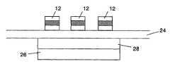
- the protectionis aimed at reverse engineering from the top, i.e. that side of a substrate 24 onto which the MRAM-cells 12 are implemented.
- a soft magnetic layer 26below the plane of the MRAM-cells 12 , with an additional permanent magnet 28 between the MRAM-cells 12 and this soft-magnetic layer 26 , the protection works against reverse engineering from the substrate-side.
- This protectionmay be placed at the backside of the substrate 24 , as shown in FIG. 4 .
- the protection as shown in FIG. 4can be combined e.g. with a security device 14 next to the array 10 , as in FIG. 1 or with a security device next to the array 10 and a magnetic field shaping device 22 as in FIG. 3 .
- distancesshould be chosen such that the field from magnet 16 will not be influenced too much by the soft magnetic layer 26 , and that the field from magnet 28 will not be influenced too much by the soft magnetic layers 18 and/or 22 .
- protection at the top and bottom side of the substrate 24can be alternating i.e. when there is a topside protection 14 in a certain area of the memory array 10 there is no back protection and vice versa.
- the present inventionprovides a hardware protection against tampering that can easily be added to an embedded or stand-alone MRAM.
- securityis essential, such as for example in smartcards, or in which the integrity of data is crucial, e.g. program code of the operation system in embedded MRAM in a System on Chip (SoC)
- SoCSystem on Chip
- the protection according to the present inventionhas the advantage of being passive, i.e. it does not require power to operate.
Landscapes
- Engineering & Computer Science (AREA)
- Computer Hardware Design (AREA)
- Physics & Mathematics (AREA)
- General Physics & Mathematics (AREA)
- Microelectronics & Electronic Packaging (AREA)
- Condensed Matter Physics & Semiconductors (AREA)
- Power Engineering (AREA)
- Computer Security & Cryptography (AREA)
- General Engineering & Computer Science (AREA)
- Theoretical Computer Science (AREA)
- Storage Device Security (AREA)
Abstract
Description
Claims (6)
Priority Applications (2)
| Application Number | Priority Date | Filing Date | Title |
|---|---|---|---|
| US10/539,548US7712147B2 (en) | 2002-12-18 | 2003-12-15 | Method and device for protection of an mram device against tampering |
| US12/708,874US8261367B2 (en) | 2003-02-20 | 2010-02-19 | Method and device for protection of an MRAM device against tampering |
Applications Claiming Priority (8)
| Application Number | Priority Date | Filing Date | Title |
|---|---|---|---|
| US43482902P | 2002-12-18 | 2002-12-18 | |
| US43452002P | 2002-12-18 | 2002-12-18 | |
| US43998603P | 2003-01-14 | 2003-01-14 | |
| EP03100402 | 2003-02-20 | ||
| EP03100402 | 2003-02-20 | ||
| EP03100402.1 | 2003-02-20 | ||
| US10/539,548US7712147B2 (en) | 2002-12-18 | 2003-12-15 | Method and device for protection of an mram device against tampering |
| PCT/IB2003/006005WO2004055824A2 (en) | 2002-12-18 | 2003-12-15 | Method and device for protection of an mram device against tampering |
Related Child Applications (1)
| Application Number | Title | Priority Date | Filing Date |
|---|---|---|---|
| US12/708,874ContinuationUS8261367B2 (en) | 2003-02-20 | 2010-02-19 | Method and device for protection of an MRAM device against tampering |
Publications (2)
| Publication Number | Publication Date |
|---|---|
| US20060179490A1 US20060179490A1 (en) | 2006-08-10 |
| US7712147B2true US7712147B2 (en) | 2010-05-04 |
Family
ID=32600965
Family Applications (1)
| Application Number | Title | Priority Date | Filing Date |
|---|---|---|---|
| US10/539,548Active2027-09-02US7712147B2 (en) | 2002-12-18 | 2003-12-15 | Method and device for protection of an mram device against tampering |
Country Status (1)
| Country | Link |
|---|---|
| US (1) | US7712147B2 (en) |
Cited By (13)
| Publication number | Priority date | Publication date | Assignee | Title |
|---|---|---|---|---|
| US20100050275A1 (en)* | 2008-08-21 | 2010-02-25 | Burch Kenneth R | Device that can be rendered useless and method thereof |
| US20100146641A1 (en)* | 2003-02-20 | 2010-06-10 | Nxp B.V. | Method and device for protection of an mram device against tampering |
| US20110185483A1 (en)* | 2008-06-23 | 2011-08-04 | Christopher Mark Lewis | Articulated body armour |
| US8213207B2 (en) | 2010-08-25 | 2012-07-03 | Honeywell International Inc. | Printed board assembly movement detection |
| US20130241014A1 (en)* | 2012-03-13 | 2013-09-19 | Honeywell International Inc. | Magnetoresistive random access memory (mram) package including a multilayer magnetic security structure |
| US8854870B2 (en) | 2012-03-13 | 2014-10-07 | Honeywell International Inc. | Magnetoresistive random access memory (MRAM) die including an integrated magnetic security structure |
| US8909942B1 (en) | 2012-03-30 | 2014-12-09 | Western Digital Technologies, Inc. | MRAM-based security for data storage systems |
| US9153332B2 (en) | 2012-10-23 | 2015-10-06 | Samsung Electronics Co., Ltd. | Data storage device, controller, and operating method of data storage device |
| US9251099B2 (en) | 2012-11-30 | 2016-02-02 | Samsung Electronics Co., Ltd. | Nonvolatile memory modules and authorization systems and operating methods thereof |
| US20170116440A1 (en)* | 2014-06-27 | 2017-04-27 | Jerry Huang | System for data protection in power off mode |
| US10192039B2 (en) | 2014-06-27 | 2019-01-29 | Microsoft Technology Licensing, Llc | System for context-based data protection |
| US10372937B2 (en) | 2014-06-27 | 2019-08-06 | Microsoft Technology Licensing, Llc | Data protection based on user input during device boot-up, user login, and device shut-down states |
| US10423766B2 (en) | 2014-06-27 | 2019-09-24 | Microsoft Technology Licensing, Llc | Data protection system based on user input patterns on device |
Families Citing this family (7)
| Publication number | Priority date | Publication date | Assignee | Title |
|---|---|---|---|---|
| US7224634B2 (en)* | 2002-12-18 | 2007-05-29 | Nxp B.V. | Hardware security device for magnetic memory cells |
| US20060152173A1 (en)* | 2004-12-27 | 2006-07-13 | M-Systems Flash Disk Pioneers Ltd. | Method and apparatus for intentionally damaging a solid-state disk |
| US7468664B2 (en)* | 2006-04-20 | 2008-12-23 | Nve Corporation | Enclosure tamper detection and protection |
| US20070279969A1 (en)* | 2006-06-02 | 2007-12-06 | Raytheon Company | Intrusion detection apparatus and method |
| EP2135254B1 (en) | 2007-03-09 | 2016-05-25 | NVE Corporation | Stressed magnetoresistive tamper detection devices |
| US9218509B2 (en) | 2013-02-08 | 2015-12-22 | Everspin Technologies, Inc. | Response to tamper detection in a memory device |
| WO2014124271A1 (en)* | 2013-02-08 | 2014-08-14 | Everspin Technologies, Inc. | Tamper detection and response in a memory device |
Citations (14)
| Publication number | Priority date | Publication date | Assignee | Title |
|---|---|---|---|---|
| US5902690A (en)* | 1997-02-25 | 1999-05-11 | Motorola, Inc. | Stray magnetic shielding for a non-volatile MRAM |
| US6172902B1 (en)* | 1998-08-12 | 2001-01-09 | Ecole Polytechnique Federale De Lausanne (Epfl) | Non-volatile magnetic random access memory |
| US6219789B1 (en)* | 1995-07-20 | 2001-04-17 | Dallas Semiconductor Corporation | Microprocessor with coprocessing capabilities for secure transactions and quick clearing capabilities |
| US20010033012A1 (en) | 1999-12-30 | 2001-10-25 | Koemmerling Oliver | Anti tamper encapsulation for an integrated circuit |
| US20020008988A1 (en)* | 2000-06-23 | 2002-01-24 | Koninklijke Philips Electronics N.V. | Magnetic memory |
| US6501678B1 (en)* | 1999-06-18 | 2002-12-31 | Koninklijke Philips Electronics N.V. | Magnetic systems with irreversible characteristics and a method of manufacturing and repairing and operating such systems |
| US6522577B1 (en)* | 2002-06-05 | 2003-02-18 | Micron Technology, Inc. | System and method for enabling chip level erasing and writing for magnetic random access memory devices |
| US20040032010A1 (en)* | 2002-08-14 | 2004-02-19 | Kools Jacques Constant Stefan | Amorphous soft magnetic shielding and keeper for MRAM devices |
| US20050230788A1 (en)* | 2004-02-23 | 2005-10-20 | Yoshihiro Kato | Magnetic shield member, magnetic shield structure, and magnetic memory device |
| US20060081497A1 (en)* | 2002-12-18 | 2006-04-20 | Koninklijke Philips Electronics N.V. | Tamper-resistant packaging and approach |
| US20060108668A1 (en)* | 2002-12-18 | 2006-05-25 | Carl Knudsen | Tamper resistant packaging and approach |
| US20060146597A1 (en)* | 2002-12-18 | 2006-07-06 | Lenssen Kars-Michiel H | Hardware security device for magnetic memory cells |
| US7205883B2 (en)* | 2002-10-07 | 2007-04-17 | Safenet, Inc. | Tamper detection and secure power failure recovery circuit |
| US20070139989A1 (en)* | 2003-01-14 | 2007-06-21 | Koninklijke Philips Electronics N.V. | Tamper-resistant packaging and approach using magnetically-set data |
- 2003
- 2003-12-15USUS10/539,548patent/US7712147B2/enactiveActive
Patent Citations (18)
| Publication number | Priority date | Publication date | Assignee | Title |
|---|---|---|---|---|
| US6219789B1 (en)* | 1995-07-20 | 2001-04-17 | Dallas Semiconductor Corporation | Microprocessor with coprocessing capabilities for secure transactions and quick clearing capabilities |
| US5902690A (en)* | 1997-02-25 | 1999-05-11 | Motorola, Inc. | Stray magnetic shielding for a non-volatile MRAM |
| US6172902B1 (en)* | 1998-08-12 | 2001-01-09 | Ecole Polytechnique Federale De Lausanne (Epfl) | Non-volatile magnetic random access memory |
| US6501678B1 (en)* | 1999-06-18 | 2002-12-31 | Koninklijke Philips Electronics N.V. | Magnetic systems with irreversible characteristics and a method of manufacturing and repairing and operating such systems |
| US20010033012A1 (en) | 1999-12-30 | 2001-10-25 | Koemmerling Oliver | Anti tamper encapsulation for an integrated circuit |
| US20020008988A1 (en)* | 2000-06-23 | 2002-01-24 | Koninklijke Philips Electronics N.V. | Magnetic memory |
| US6522577B1 (en)* | 2002-06-05 | 2003-02-18 | Micron Technology, Inc. | System and method for enabling chip level erasing and writing for magnetic random access memory devices |
| US6650564B1 (en)* | 2002-06-05 | 2003-11-18 | Micron Technology, Inc. | System and method for enabling chip level erasing and writing for magnetic random access memory devices |
| US20040032010A1 (en)* | 2002-08-14 | 2004-02-19 | Kools Jacques Constant Stefan | Amorphous soft magnetic shielding and keeper for MRAM devices |
| US20050045998A1 (en)* | 2002-08-14 | 2005-03-03 | Kools Jacques Constant Stefan | Amorphous soft magnetic shielding and keeper for MRAM devices |
| US7205883B2 (en)* | 2002-10-07 | 2007-04-17 | Safenet, Inc. | Tamper detection and secure power failure recovery circuit |
| US20060081497A1 (en)* | 2002-12-18 | 2006-04-20 | Koninklijke Philips Electronics N.V. | Tamper-resistant packaging and approach |
| US20060108668A1 (en)* | 2002-12-18 | 2006-05-25 | Carl Knudsen | Tamper resistant packaging and approach |
| US20060146597A1 (en)* | 2002-12-18 | 2006-07-06 | Lenssen Kars-Michiel H | Hardware security device for magnetic memory cells |
| US7224634B2 (en)* | 2002-12-18 | 2007-05-29 | Nxp B.V. | Hardware security device for magnetic memory cells |
| US7485976B2 (en)* | 2002-12-18 | 2009-02-03 | Nxp B.V. | Tamper resistant packaging and approach |
| US20070139989A1 (en)* | 2003-01-14 | 2007-06-21 | Koninklijke Philips Electronics N.V. | Tamper-resistant packaging and approach using magnetically-set data |
| US20050230788A1 (en)* | 2004-02-23 | 2005-10-20 | Yoshihiro Kato | Magnetic shield member, magnetic shield structure, and magnetic memory device |
Non-Patent Citations (1)
| Title |
|---|
| Lenssen, Kars-Michiel H. et al. Expectations of MRAM in comparison with other non-volatile memory technologies. NVMT Symposium. 2000. p. 1-24.* |
Cited By (17)
| Publication number | Priority date | Publication date | Assignee | Title |
|---|---|---|---|---|
| US20100146641A1 (en)* | 2003-02-20 | 2010-06-10 | Nxp B.V. | Method and device for protection of an mram device against tampering |
| US8261367B2 (en)* | 2003-02-20 | 2012-09-04 | Crocus Technology, Inc. | Method and device for protection of an MRAM device against tampering |
| US20110185483A1 (en)* | 2008-06-23 | 2011-08-04 | Christopher Mark Lewis | Articulated body armour |
| US20100050275A1 (en)* | 2008-08-21 | 2010-02-25 | Burch Kenneth R | Device that can be rendered useless and method thereof |
| US8254161B2 (en)* | 2008-08-21 | 2012-08-28 | Freescale Semiconductor, Inc. | Device that can be rendered useless and method thereof |
| US8213207B2 (en) | 2010-08-25 | 2012-07-03 | Honeywell International Inc. | Printed board assembly movement detection |
| US8854870B2 (en) | 2012-03-13 | 2014-10-07 | Honeywell International Inc. | Magnetoresistive random access memory (MRAM) die including an integrated magnetic security structure |
| US8811072B2 (en)* | 2012-03-13 | 2014-08-19 | Honeywell International Inc. | Magnetoresistive random access memory (MRAM) package including a multilayer magnetic security structure |
| US20130241014A1 (en)* | 2012-03-13 | 2013-09-19 | Honeywell International Inc. | Magnetoresistive random access memory (mram) package including a multilayer magnetic security structure |
| US8909942B1 (en) | 2012-03-30 | 2014-12-09 | Western Digital Technologies, Inc. | MRAM-based security for data storage systems |
| US9153332B2 (en) | 2012-10-23 | 2015-10-06 | Samsung Electronics Co., Ltd. | Data storage device, controller, and operating method of data storage device |
| US9251099B2 (en) | 2012-11-30 | 2016-02-02 | Samsung Electronics Co., Ltd. | Nonvolatile memory modules and authorization systems and operating methods thereof |
| US20170116440A1 (en)* | 2014-06-27 | 2017-04-27 | Jerry Huang | System for data protection in power off mode |
| US10192039B2 (en) | 2014-06-27 | 2019-01-29 | Microsoft Technology Licensing, Llc | System for context-based data protection |
| US10372937B2 (en) | 2014-06-27 | 2019-08-06 | Microsoft Technology Licensing, Llc | Data protection based on user input during device boot-up, user login, and device shut-down states |
| US10423766B2 (en) | 2014-06-27 | 2019-09-24 | Microsoft Technology Licensing, Llc | Data protection system based on user input patterns on device |
| US10474849B2 (en)* | 2014-06-27 | 2019-11-12 | Microsoft Technology Licensing, Llc | System for data protection in power off mode |
Also Published As
| Publication number | Publication date |
|---|---|
| US20060179490A1 (en) | 2006-08-10 |
Similar Documents
| Publication | Publication Date | Title |
|---|---|---|
| US8261367B2 (en) | Method and device for protection of an MRAM device against tampering | |
| US7712147B2 (en) | Method and device for protection of an mram device against tampering | |
| CN100547678C (en) | Hardware security device and method for magnetic storage unit | |
| US8294577B2 (en) | Stressed magnetoresistive tamper detection devices | |
| US7468664B2 (en) | Enclosure tamper detection and protection | |
| US7911830B2 (en) | Scalable nonvolatile memory | |
| US20050254288A1 (en) | Magnetic random access memory and method of writing data in magnetic random access memory | |
| US20070058422A1 (en) | Programmable magnetic memory device | |
| US20140062530A1 (en) | Switching mechanism of magnetic storage cell and logic unit using current induced domain wall motions | |
| US7224634B2 (en) | Hardware security device for magnetic memory cells | |
| US7411814B2 (en) | Programmable magnetic memory device FP-MRAM | |
| JP2004282074A (en) | Magnetic sensor | |
| EP1690263B1 (en) | Data retention indicator for magnetic memories | |
| KR20050048667A (en) | Read-only magnetic memory device mrom | |
| EP1576615B1 (en) | Hardware security device for magnetic memory cells |
Legal Events
| Date | Code | Title | Description |
|---|---|---|---|
| AS | Assignment | Owner name:KONINKLIJKE PHILIPS ELECTRONICS N.V.,NETHERLANDS Free format text:ASSIGNMENT OF ASSIGNORS INTEREST;ASSIGNORS:LENSSEN, KARS-MICHIEL;JOCHEMSEN, ROBERT;REEL/FRAME:017440/0936 Effective date:20040715 Owner name:KONINKLIJKE PHILIPS ELECTRONICS N.V., NETHERLANDS Free format text:ASSIGNMENT OF ASSIGNORS INTEREST;ASSIGNORS:LENSSEN, KARS-MICHIEL;JOCHEMSEN, ROBERT;REEL/FRAME:017440/0936 Effective date:20040715 | |
| AS | Assignment | Owner name:NXP B.V., NETHERLANDS Free format text:ASSIGNMENT OF ASSIGNORS INTEREST;ASSIGNOR:KONINKLIJKE PHILIPS ELECTRONICS N.V.;REEL/FRAME:021085/0959 Effective date:20080423 Owner name:NXP B.V.,NETHERLANDS Free format text:ASSIGNMENT OF ASSIGNORS INTEREST;ASSIGNOR:KONINKLIJKE PHILIPS ELECTRONICS N.V.;REEL/FRAME:021085/0959 Effective date:20080423 | |
| STCF | Information on status: patent grant | Free format text:PATENTED CASE | |
| AS | Assignment | Owner name:NXP B.V., NETHERLANDS Free format text:LIEN;ASSIGNOR:CROCUS TECHNOLOGY, INC.;REEL/FRAME:027222/0049 Effective date:20110805 | |
| AS | Assignment | Owner name:CROCUS TECHNOLOGY, INC., CALIFORNIA Free format text:ASSIGNMENT OF ASSIGNORS INTEREST;ASSIGNOR:NXP B.V.;REEL/FRAME:028092/0605 Effective date:20110411 | |
| FPAY | Fee payment | Year of fee payment:4 | |
| AS | Assignment | Owner name:KREOS CAPITAL IV (LUXEMBOURG) SARL, UNITED KINGDOM Free format text:SECURITY INTEREST;ASSIGNOR:CROCUS TECHNOLOGY, INC.;REEL/FRAME:033917/0259 Effective date:20140912 | |
| AS | Assignment | Owner name:KREOS CAPITAL IV (LUXEMBOURG) SARL, UNITED KINGDOM Free format text:SECURITY INTEREST;ASSIGNOR:CROCUS TECHNOLOGY, INC.;REEL/FRAME:036031/0327 Effective date:20150603 | |
| MAFP | Maintenance fee payment | Free format text:PAYMENT OF MAINTENANCE FEE, 8TH YEAR, LARGE ENTITY (ORIGINAL EVENT CODE: M1552) Year of fee payment:8 | |
| AS | Assignment | Owner name:CROCUS TECHNOLOGY, INC., CALIFORNIA Free format text:RELEASE BY SECURED PARTY;ASSIGNOR:KREOS CAPITAL IV (LUXEMBOURG) SARL;REEL/FRAME:045871/0622 Effective date:20180405 Owner name:CROCUS TECHNOLOGY, INC., CALIFORNIA Free format text:RELEASE BY SECURED PARTY;ASSIGNOR:KREOS CAPITAL IV (LUXEMBOURG) SARL;REEL/FRAME:045865/0555 Effective date:20180405 | |
| AS | Assignment | Owner name:LLC "SBERBANK INVESTMENTS", RUSSIAN FEDERATION Free format text:SECURITY INTEREST;ASSIGNOR:CROCUS TECHNOLOGY, INC.;REEL/FRAME:045938/0810 Effective date:20180314 | |
| MAFP | Maintenance fee payment | Free format text:PAYMENT OF MAINTENANCE FEE, 12TH YEAR, LARGE ENTITY (ORIGINAL EVENT CODE: M1553); ENTITY STATUS OF PATENT OWNER: LARGE ENTITY Year of fee payment:12 | |
| AS | Assignment | Owner name:CROCUS TECHNOLOGY, INC., FRANCE Free format text:RELEASE BY SECURED PARTY;ASSIGNOR:LLC "SBERBANK INVESTMENTS";REEL/FRAME:064783/0420 Effective date:20220412 | |
| AS | Assignment | Owner name:NXP B.V., NETHERLANDS Free format text:CORRECTIVE ASSIGNMENT TO CORRECT THE THE SPELLING OF THE CONVEYING PARTY NAME AND ADDRESS ON THE DOCUMENT. PREVIOUSLY RECORDED AT REEL: 02722 FRAME: 0049. ASSIGNOR(S) HEREBY CONFIRMS THE ASSIGNMENT;ASSIGNOR:CROCUS TECHNOLOGY INC.;REEL/FRAME:065345/0304 Effective date:20110805 Owner name:CROCUS TECHNOLOGY INC., CALIFORNIA Free format text:CORRECTIVE ASSIGNMENT TO CORRECT THE TYPOGRAPHICAL ERROR IN THE NAME OF THE RECEIVING PARTY AND TO UPDATE THE ADDRESS OF THE RECEIVING PARTY PREVIOUSLY RECORDED AT REEL: 028092 FRAME: 0605. ASSIGNOR(S) HEREBY CONFIRMS THE ASSIGNMENT;ASSIGNOR:NXP B.V.;REEL/FRAME:065350/0786 Effective date:20110411 Owner name:CROCUS TECHNOLOGY INC., CALIFORNIA Free format text:RELEASE BY SECURED PARTY;ASSIGNOR:NXP B.V.;REEL/FRAME:065334/0488 Effective date:20231024 | |
| AS | Assignment | Owner name:ALLEGRO MICROSYSTEMS, LLC, NEW HAMPSHIRE Free format text:ASSIGNMENT OF ASSIGNORS INTEREST;ASSIGNOR:CROCUS TECHNOLOGY SA;REEL/FRAME:066350/0669 Effective date:20240101 |