US7711926B2 - Mapping system and method for instruction set processing - Google Patents
Mapping system and method for instruction set processingDownload PDFInfo
- Publication number
- US7711926B2 US7711926B2US09/836,541US83654101AUS7711926B2US 7711926 B2US7711926 B2US 7711926B2US 83654101 AUS83654101 AUS 83654101AUS 7711926 B2US7711926 B2US 7711926B2
- Authority
- US
- United States
- Prior art keywords
- instruction
- piwf
- tag
- instructions
- mapping
- Prior art date
- Legal status (The legal status is an assumption and is not a legal conclusion. Google has not performed a legal analysis and makes no representation as to the accuracy of the status listed.)
- Expired - Lifetime, expires
Links
Images


Classifications
- G—PHYSICS
- G06—COMPUTING OR CALCULATING; COUNTING
- G06F—ELECTRIC DIGITAL DATA PROCESSING
- G06F12/00—Accessing, addressing or allocating within memory systems or architectures
- G06F12/02—Addressing or allocation; Relocation
- G06F12/08—Addressing or allocation; Relocation in hierarchically structured memory systems, e.g. virtual memory systems
- G06F12/0802—Addressing of a memory level in which the access to the desired data or data block requires associative addressing means, e.g. caches
- G06F12/0864—Addressing of a memory level in which the access to the desired data or data block requires associative addressing means, e.g. caches using pseudo-associative means, e.g. set-associative or hashing
- G—PHYSICS
- G06—COMPUTING OR CALCULATING; COUNTING
- G06F—ELECTRIC DIGITAL DATA PROCESSING
- G06F9/00—Arrangements for program control, e.g. control units
- G06F9/06—Arrangements for program control, e.g. control units using stored programs, i.e. using an internal store of processing equipment to receive or retain programs
- G06F9/30—Arrangements for executing machine instructions, e.g. instruction decode
- G06F9/3017—Runtime instruction translation, e.g. macros
- G06F9/30174—Runtime instruction translation, e.g. macros for non-native instruction set, e.g. Javabyte, legacy code
- G—PHYSICS
- G06—COMPUTING OR CALCULATING; COUNTING
- G06F—ELECTRIC DIGITAL DATA PROCESSING
- G06F12/00—Accessing, addressing or allocating within memory systems or architectures
- G06F12/02—Addressing or allocation; Relocation
- G06F12/08—Addressing or allocation; Relocation in hierarchically structured memory systems, e.g. virtual memory systems
- G06F12/0802—Addressing of a memory level in which the access to the desired data or data block requires associative addressing means, e.g. caches
- G06F12/0875—Addressing of a memory level in which the access to the desired data or data block requires associative addressing means, e.g. caches with dedicated cache, e.g. instruction or stack
Definitions
- the present inventionrelates generally to computer architecture, and more specifically to a processor capable of executing instructions from multiple instruction sets.
- Such instructionsmay execute routines slower than those from the first instruction set (because more and possibly different instructions are required to carry out the same function), but the narrower format contributes to a potential reduction in overall memory space required.
- a third instruction setcould be made available to provide backwards compatibility to earlier generation machines that, again, may utilize instruction width formats of differing size (e.g., older 16-bit machines).
- a fourth (or more) instruction setcould be made available to provide upwards compatibility to new developments in instruction sets that may also require different instruction width formats (e.g., 8-bit JAVA bytecodes).
- mappingmay be achieved in such a system through a series of operations carried out in one or more pipeline stages (of a pipelined processor). These operations include reading a plurality of instructions from a cache memory, and processing such instructions by tag comparing each instruction, selecting a desired instruction from the plurality (based on the tag compare) and then mapping the desired instruction.
- these operationsinclude reading a plurality of instructions from a cache memory, and processing such instructions by tag comparing each instruction, selecting a desired instruction from the plurality (based on the tag compare) and then mapping the desired instruction.
- the processing of these instructionsresults in a branch penalty and/or increased cycle time.
- the tag compare devicecompares each tag having an associated data component in cache memory with the address being sought to determine if the cache contains a “hit.” If there is not a hit, the instruction of the address being sought is read from main memory. If there is a hit in the cache, the tag comparison device transmits a signal to the multiplexor indicating which of the mapped instructions is the “desired” instruction.
- the multiplexorthen selects the desired instruction and transmits it downstream to the execution core.
- the systemreduces processor cycle time and results in improved performance of the processor.
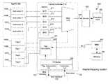
- FIG. 1is a block diagram illustrating the system architecture of a traditional serial mapping system.
- FIG. 2is a block diagram illustrating the system architecture of a parallel mapping system utilized in the present invention.
- FIG. 3is a timing diagram depicting a comparison of time in the system of FIG. 1 with that of FIG. 2 .
- FIG. 4is a flowchart representing the general operational flow of the steps executed in the parallel mapping system of the present invention.
- FIG. 5is a block diagram illustrating the system architecture of a parallel mapping system utilized in an alternate embodiment of the present invention.
- the present inventionis described in the environment of a processor that maps instructions of a first instruction set to a predetermined instruction width format (“PIWF”) that is sufficiently wide to, and does, accommodate two or more instruction sets.
- the PIWFis wider than the instruction width formats of the plurality of instructions sets supported by the host computer system.
- the extra widthmay be used to support functionality that is unique and exclusive to each respective instruction set. That is, a first instruction set may have unique functionality not available in one or more other instruction sets. Further, a second instruction set may have unique functionality that is not available in the first instruction set.
- the PIWFis the same width as at least one of the instruction width formats of the instruction sets supported by the computer system.
- the PIWFcould be identical to one of the supported instruction sets. For example, if one of the supported instruction sets has an instruction width of 32 bits, the PIWF would be identical to such set if the PIWF also had a width of 32 bits and had the same encoding (with no additions or deletions) as the supported instruction set.
- the PIWFis a format with a sufficient number of bits to provide a corresponding representation for each instruction in the plurality of instruction sets supported by the host computer system. Each instruction in the plurality of instruction sets is mapped to a PIWF configuration representing that instruction.
- the PIWFmay itself be an instruction set (if identical to a supported instruction set) or it may be an intermediate instruction representation (if different from all the supported instructions sets). In either case, a decoder is required to decode the PIWF for execution by a processor core.
- 16-bit instructionsare mapped to a 34-bit PIWF configuration that supports 16-bit and 32-bit instructions.
- the PIWFmay have fewer or more than 34 bits.
- This environmentis used for purposes of illustration. The invention, however, is not so limited. A person skilled in the art will recognize that the invention has applicability for mapping instructions (or, more generically, “data”) from any first format to any PIWF configuration.
- each 32-bit instruction in the exemplary embodimentmust also be mapped to a PIWF configuration. This may be achieved through a mapper scheme (as described below), bit stuffing, or any other mapping method known to those skilled in the art.
- FIG. 1the system architecture of a traditional serial mapping system utilized by a processor executing a computer instruction fetch operation is shown.
- a read operationexecuted by a processor or central processing unit (CPU) 100 .
- CPUcentral processing unit
- a cache setis accessed from a cache memory 102 by a cache controller 110 .
- each cache setis comprised of a set of sixteen byte fields or lines plus respective tag components.
- the cache setincludes four cache lines.
- Each cache linecomprises a data component 140 A-D and a tag component 145 A-D.
- data component 140 A and its corresponding tag component 145 Acombine to form one cache line.
- Data component 140 B and tag component 145 Bcombine to form a second cache line.
- Data component 140 C and tag component 145 Ccombine to form a third cache line.
- Data component 140 D and tag component 145 Dcombine to form a fourth cache line. This configuration is present for each line in the cache.
- each data component 140 of a cache linean instruction is stored, i.e. an opcode value and operand description.
- data component 140 Acontains instruction 0.
- Data component 140 Bcontains instruction 1;
- data component 140 Ccontains instruction 2;
- data component 140 Dcontains instruction 3, and so forth. Note, however, that instructions in multiple lines of the same set (i.e., instructions 0-3) are not sequential instructions.
- the numbering convention 0, 1, 2 and 3is used simply for convenience and does not imply an ordering.
- Memory Management Unit (MMU) 160generates a sought address.
- a tag component of the sought addressis used to determine if the instruction being sought is actually stored in cache memory 102 . If the instruction sought resides in cache memory 102 , the cache is said to contain a “hit.” If not, a miss occurs and the instruction sought must be read into cache memory 102 from main memory 104 .
- tag component 145 Acontains tag 0.
- Tag 0represents the tag associated with instruction 0, stored in data component 140 A
- tag 1represents the tag associated with instruction 1, stored in data component 140 B
- tag 2represents the tag associated with instruction 2, stored in data component 140 C
- tag 3represents the tag associated with instruction 3, stored in data component 140 D, etc.
- each sixteen bit instructionmust be mapped to a PIWF configuration.
- the cache controller 110 of the serial mapping system depicted in FIG. 1contains a mapper 120 for mapping each instruction of a first instruction set to a corresponding PIWF configuration; a multiplexor 115 ; and a tag comparator 125 .
- the cache linecomprising data component 140 A and tag component 145 A is accessed.
- Instruction 0, stored in data component 140 Ais read into multiplexer 115 .
- instruction 1, stored in data component 140 Bis read into multiplexor 115 .
- Instruction 2, stored in data component 140 Cis read into multiplexor 115 .
- Instruction 3, stored in data component 140 Dis read into multiplexor 115 , and so forth.
- Tag comparator 125performs a tag comparison operation on all of the tags stored in the tag components 145 . More specifically, tag comparator 125 compares tag 0, associated with instruction 0, to the address generated by MMU 160 , the “sought address.” Likewise, tag comparator 125 compares tag 1, associated with instruction 1, to the tag of the sought address. Tag comparator 125 compares tag 2, associated with instruction 2, to the tag of the sought address. Tag comparator 125 compares tag 3, associated with instruction 3, to the tag of the sought address. These tag comparison operations are executed in parallel.
- the cachedoes not contain a hit, and the value sought must be read from main memory. If the tag of the sought address matches a tag associated with any data stored in any particular cache line, the cache contains a hit.
- the cachecontains a hit because tag 2 is the value stored in tag component 145 C, which is associated with data component 140 C.
- instruction 2 stored in data component 140 Cis the desired instruction because its associated tag, tag 2, matches the tag of the sought address.
- Tag comparator 125then transmits an indicator signal to multiplexor 115 to select the desired instruction. Multiplexor 115 then selects the desired instruction. In the above referenced example, where the tag comparison device located instruction 2, the desired instruction, tag comparator 125 transmits an indication to multiplexor 115 to select instruction 2.
- Multiplexor 115receives the indicator signal from tag comparator 125 , selects the desired instruction, and then transmits the desired instruction to mapper 120 .
- Mapper 120maps the desired instruction of the first instruction set to a PIWF configuration and transmits a mapped instruction 150 to a decoder 152 .
- Decoder 152decodes the mapped instruction and provides control signals to execution core 155 for execution.
- fill buffer 130is present and serves as a staging point for cache memory.
- Fill buffer 130comprises a tag component 131 and its associated data component or instruction 132 . If the processor determines that there was a “miss” upon reading instruction cache 102 , the processor accesses bus interface 103 to obtain instruction 132 from memory 104 (interconnection of bus interface 103 and memory 104 not shown). The processor supplies the memory address 133 of the instruction that was not identified in the cache memory 102 to memory 104 via bus interface 103 .
- fill buffer 130is accessed.
- Tag 131 of fill buffer 130is compared to the tag of the sought address. If there is a hit, tag comparator 125 transmits a signal to multiplexor 125 to select data 132 because its associated tag 131 was the hit. Multiplexor 125 then passes the selected instruction to be processed to mapper 120 and transmits it downstream to the execution core, just as if the selected instruction had been stored in cache memory.
- downstreamis used throughout this document to reference the direction that data flows through processor 100 over time (i.e., heading away from the cache controller to the execution core, etc.).
- upstreamis used to reference the reverse direction (i.e., heading away from the execution core to the cache controller).
- FIG. 2illustrates the system architecture of a parallel mapping system utilized by a CPU or processor 200 initiating a computer instruction fetch operation.
- a cache setis accessed by cache controller 210 .
- Each cache setis comprised of four sixteen byte lines or fields plus respective tag components.
- Each cache linecomprises a data component and a tag component, as described above.
- Instruction fetchbegins as described above with respect to FIG. 1 . However, the mapping and selection processes are different. Continuing with the example of the read operation, each of the data components 140 is read in parallel into a corresponding one of a plurality of mappers 211 - 214 . For example, instruction 0 stored in data component 140 A is read into corresponding mapper 211 . Simultaneously, instruction 1 stored in data component 140 B is read into corresponding mapper 212 . Instruction 2, stored in data component 140 C, is simultaneously read into corresponding mapper 213 . Instruction 3 stored in data component 140 D is simultaneously read into mapper 214 . As further described below, an instruction is provided to mapper 215 via line 244 .
- each instruction of a first instruction set stored in cache memory 102is read into a corresponding one of the plurality of mappers 211 - 214 in parallel.
- Each of the plurality of mappers 211 - 214maps an instruction of a first instruction set to a PIWF configuration.
- Each of the mapped instructionsis then provided to multiplexor 115 for selection.
- tag comparator 125performs a tag comparison operation on all of the tags stored in tag components 145 . More specifically, tag comparator 125 compares tag 0, associated with instruction 0, to the tag of the sought address. Likewise, tag comparator 125 compares tag 1, associated with instruction 1, to the tag of the sought address. Tag comparator 125 compares tag 2, associated with instruction 2, to the tag of the sought address. Tag comparator 125 compares tag 3, associated with instruction 3, to the tag of the sought address. These tag comparison operations continue until the tag associated with the last line of data in the cache is compared to the tag of the sought address.
- the cachedoes not contain a hit, and the value sought must be read from main memory.
- the cachecontains a hit. For example, if the tag of the sought address is tag 2, the cache contains a hit because tag 2 is the value stored in tag component 145 C, which is associated with data component 140 C. Thus, instruction 2, stored in data component 140 C, is the desired instruction because its associated tag, tag 2, matches the tag associated with the instruction sought.
- Tag comparator 125provides an indicator signal to multiplexor 115 to select the value located in the cache (i.e., the desired instruction). Multiplexor 115 then selects the desired instruction. In the above referenced example, where tag comparator 125 identified instruction 2, the desired instruction, tag comparator 125 transmits an indicator signal to multiplexor 115 to select instruction 2.
- Multiplexor 115selects the desired instruction and transmits the selected instruction to the execution core for further processing (i.e., for instruction decoding and execution).
- mappingoperations of mapping, tag comparing, and selecting a desired instruction each occur in a single pipeline stage in the present invention. By performing tag comparison in parallel with mapping, processing time is improved.
- fill buffer 130is present and serves as a staging point for cache memory 102 .
- Fill buffer 130comprises a tag component 131 and its associated data component 132 . If the processor determines that there was a “miss” upon reading instruction cache 102 , the processor accesses bus interface 103 to obtain instruction 132 from memory 104 (interconnection of bus interface 103 and memory 104 not shown). The processor supplies the memory address of the instruction that was not identified in the cache memory 102 to memory 104 via bus interface 103 . Next, just as a cache line is accessed upon the data read operation, fill buffer 130 is accessed. Thus, data 132 is read into corresponding mapper 215 . Data component 132 , containing an instruction, is then mapped to a PIWF configuration.
- Tag comparator 125compares tag 131 of fill buffer 130 to the tag of the sought address. If there is a hit, tag comparator 125 transmits a signal to multiplexor 115 . Multiplexor 115 then selects data 132 if its associated tag 131 is the hit. Multiplexor 115 then passes the selected instruction to be processed downstream to the execution core, just as if the instruction was stored in a cache line of cache 102 .
- FIG. 3is a timing diagram comparing timing of the serial system (processor 100 ) in FIG. 1 with timing of the parallel system (processor 200 ) of FIG. 2 .
- FIG. 3shows three time lines, T 1 , T 2 , and T 3 .
- Time line T 1illustrates the timing tag comparison by tag comparator 125 .
- Time line T 2illustrates the timing of instruction fetch and mapping operations by cache controller 110 of processor 100 (i.e., the serial system).
- Time line T 3illustrates the timing of instruction fetch and mapping operations by cache controller 210 of processor 200 (i.e., the parallel system).
- a tag of an instructionis fetched during period P 1 (between t 0 and t 1 ).
- Tag comparisonthen occurs during period P 2 (between t 1 and t 3 ).
- period P 3between t 3 and t 5
- instruction selectionoccurs. That is, during period P 3 , comparator 125 produces the select signal and provides it to multiplexor 115 . Note that the data path through multiplexor 115 is much faster than the select path through comparator 125 . If data arrives at multiplexor 115 prior to arrival of the select signal, the data will wait for the select signal.
- time line T 2(illustrating the timing of instruction fetch and mapping operations in the serial system)
- the data or instructionsare fetched during period P 4 (between t 0 and t 2 ).
- period P 5between t 2 and t 4
- selection by multiplexor 115awaits completion of tag comparison at period P 2 .
- the select signalis generated at time t 5 and selection occurs.
- Mappingthen occurs during period P 6 (between t 5 and t 8 ) and ends by time t 8
- time line T 3In contrast to time line T 2 , note the absence of a wait state in time line T 3 .
- time line T 3(illustrating the timing of instruction fetch and mapping operations in the parallel system), data or instructions are fetched during period P 7 (between t 0 and t 2 ). Then, during period P 8 (between t 2 and t 6 ), mapping occurs. Note that mapping occurs substantially in parallel with tag comparison. Thus, while tag comparison is being done, mapping is also being done. Mapping may complete before or after tag comparison is complete.
- mappingends at time t 6 after completion of tag comparison.
- the select signalis used during a period P 9 (between t 6 and t 7 ) to select the appropriate data/instruction fed to multiplexor 115 .
- time line T 3is shorter than T 2 . Because of the wait period P 5 in the serial system, valuable time is wasted while the system waits for the tag comparison operation to complete.
- the time saved by the parallel system of the inventionis illustrated in FIG. 3 as the difference in time between t 7 and t 8 . This time can be significant.
- FIG. 4is a flowchart representing the general operational flow of the steps executed in the parallel mapping system of the present invention.
- a step 410each sixteen bit instruction and its corresponding tag of the first instruction set is read from the instruction cache into a corresponding one of a plurality of mappers and tag comparator, respectively.
- a step 420each sixteen bit instruction of the first instruction set is mapped to a 34-bit PIWF configuration.
- the tag comparatorcompares a tag of each sixteen bit instruction to the tag of the address being sought.
- the tag comparatortransmits a signal to the multiplexor indicating the desired instruction to be selected.
- step 450the multiplexor selects the desired instruction and transmits it to the execution core.
- FIG. 5depicts an alternate embodiment of the present invention. Specifically, FIG. 5 shows a CPU 500 that is substantially identical to CPU 200 of FIG. 2 . However, mappers 211 - 215 of FIG. 2 have been replaced with partial mappers 511 - 515 in FIG. 5 . Furthermore, a mapper 520 has been added to FIG. 5 .
- Each of partial mappers 511 - 515maps only a portion of an instruction to a portion of a mapped instruction of a PIWF configuration. For example, the mapped portion may be only the portion necessary to identify operand registers. Other, less time critical, mapping can occur later.
- the partially mapped instructionsare then provide to multiplexor 115 for selection. Once the desired instruction is selected, mapper 520 completes the task of mapping the remainder of the selected instruction to a PIWF configuration.
- each of partial mappers 511 - 515can be implemented in silicon so that it occupies only a fraction of the area required to implement a full mapper. This can result in a savings of total area required to implement the mapper function as compared with the previously described embodiment which requires five full mappers.
- implementationsin addition to mapping system implementations using hardware (e.g., within a microprocessor or microcontroller), implementations also may be embodied in software disposed, for example, in a computer usable (e.g., readable) medium configured to store the software (i.e., a computer readable program code).
- the program codecauses the enablement of the functions or fabrication, or both, of the systems and techniques disclosed herein. For example, this can be accomplished through the use of general programming languages (e.g., C or C++), hardware description languages (HDL) including Verilog HDL, VHDL, and so on, or other available programming and/or circuit (i.e., schematic) capture tools.
- the program codecan be disposed in any known computer usable medium including semiconductor, magnetic disk, optical disk (e.g., CD-ROM, DVD-ROM) and as a computer data signal embodied in a computer usable (e.g., readable) transmission medium (e.g., carrier wave or any other medium including digital, optical, or analog-based medium).
- a computer usable (e.g., readable) transmission mediume.g., carrier wave or any other medium including digital, optical, or analog-based medium.
- the codecan be transmitted over communication networks including the Internet and intranets.
Landscapes
- Engineering & Computer Science (AREA)
- Theoretical Computer Science (AREA)
- Software Systems (AREA)
- Physics & Mathematics (AREA)
- General Engineering & Computer Science (AREA)
- General Physics & Mathematics (AREA)
- Advance Control (AREA)
Abstract
Description
Claims (23)
Priority Applications (1)
| Application Number | Priority Date | Filing Date | Title |
|---|---|---|---|
| US09/836,541US7711926B2 (en) | 2001-04-18 | 2001-04-18 | Mapping system and method for instruction set processing |
Applications Claiming Priority (1)
| Application Number | Priority Date | Filing Date | Title |
|---|---|---|---|
| US09/836,541US7711926B2 (en) | 2001-04-18 | 2001-04-18 | Mapping system and method for instruction set processing |
Publications (2)
| Publication Number | Publication Date |
|---|---|
| US20020156996A1 US20020156996A1 (en) | 2002-10-24 |
| US7711926B2true US7711926B2 (en) | 2010-05-04 |
Family
ID=25272185
Family Applications (1)
| Application Number | Title | Priority Date | Filing Date |
|---|---|---|---|
| US09/836,541Expired - LifetimeUS7711926B2 (en) | 2001-04-18 | 2001-04-18 | Mapping system and method for instruction set processing |
Country Status (1)
| Country | Link |
|---|---|
| US (1) | US7711926B2 (en) |
Families Citing this family (1)
| Publication number | Priority date | Publication date | Assignee | Title |
|---|---|---|---|---|
| US6826681B2 (en)* | 2001-06-18 | 2004-11-30 | Mips Technologies, Inc. | Instruction specified register value saving in allocated caller stack or not yet allocated callee stack |
Citations (63)
| Publication number | Priority date | Publication date | Assignee | Title |
|---|---|---|---|---|
| US3631405A (en) | 1969-11-12 | 1971-12-28 | Honeywell Inc | Sharing of microprograms between processors |
| US3794980A (en) | 1971-04-21 | 1974-02-26 | Cogar Corp | Apparatus and method for controlling sequential execution of instructions and nesting of subroutines in a data processor |
| US3811114A (en) | 1973-01-11 | 1974-05-14 | Honeywell Inf Systems | Data processing system having an improved overlap instruction fetch and instruction execution feature |
| US3840861A (en) | 1972-10-30 | 1974-10-08 | Amdahl Corp | Data processing system having an instruction pipeline for concurrently processing a plurality of instructions |
| US3983541A (en) | 1969-05-19 | 1976-09-28 | Burroughs Corporation | Polymorphic programmable units employing plural levels of phased sub-instruction sets |
| US4110822A (en) | 1975-03-26 | 1978-08-29 | Honeywell Information Systems, Inc. | Instruction look ahead having prefetch concurrency and pipeline features |
| US4149244A (en) | 1976-06-07 | 1979-04-10 | Amdahl Corporation | Data processing system including a program-executing secondary system controlling a program-executing primary system |
| GB2016755A (en) | 1978-03-13 | 1979-09-26 | Motorola Inc | Instruction set modifier register |
| US4229790A (en) | 1978-10-16 | 1980-10-21 | Denelcor, Inc. | Concurrent task and instruction processor and method |
| US4295193A (en) | 1979-06-29 | 1981-10-13 | International Business Machines Corporation | Machine for multiple instruction execution |
| EP0073424A2 (en) | 1981-08-26 | 1983-03-09 | Hitachi, Ltd. | Central processing unit for executing instructions of variable length |
| US4388682A (en) | 1979-09-04 | 1983-06-14 | Raytheon Company | Microprogrammable instruction translator |
| US4432056A (en) | 1979-06-05 | 1984-02-14 | Canon Kabushiki Kaisha | Programmable electronic computer |
| EP0109567A2 (en) | 1982-10-22 | 1984-05-30 | International Business Machines Corporation | Accelerated instruction mapping external to source and target instruction streams for near realtime injection into the latter |
| US4467409A (en) | 1980-08-05 | 1984-08-21 | Burroughs Corporation | Flexible computer architecture using arrays of standardized microprocessors customized for pipeline and parallel operations |
| US4484268A (en) | 1982-02-22 | 1984-11-20 | Thoma Nandor G | Apparatus and method for decoding an operation code using a plurality of multiplexed programmable logic arrays |
| US4507728A (en) | 1981-03-20 | 1985-03-26 | Fujitsu Limited | Data processing system for parallel processing of different instructions |
| EP0170398A2 (en) | 1984-06-28 | 1986-02-05 | Unisys Corporation | Programme scanner for a processor having plural data and instruction streams |
| US4685080A (en) | 1982-02-22 | 1987-08-04 | International Business Machines Corp. | Microword generation mechanism utilizing separate programmable logic arrays for first and second microwords |
| US4724517A (en) | 1982-11-26 | 1988-02-09 | Inmos Limited | Microcomputer with prefixing functions |
| US4777594A (en) | 1983-07-11 | 1988-10-11 | Prime Computer, Inc. | Data processing apparatus and method employing instruction flow prediction |
| US4782441A (en) | 1985-06-14 | 1988-11-01 | Hitachi, Ltd. | Vector processor capable of parallely executing instructions and reserving execution status order for restarting interrupted executions |
| US4876639A (en) | 1983-09-20 | 1989-10-24 | Mensch Jr William D | Method and circuitry for causing sixteen bit microprocessor to execute eight bit op codes to produce either internal sixteen bit operation or internal eight bit operation in accordance with an emulation bit |
| US5031096A (en) | 1988-06-30 | 1991-07-09 | International Business Machines Corporation | Method and apparatus for compressing the execution time of an instruction stream executing in a pipelined processor |
| US5115500A (en) | 1988-01-11 | 1992-05-19 | International Business Machines Corporation | Plural incompatible instruction format decode method and apparatus |
| US5132898A (en) | 1987-09-30 | 1992-07-21 | Mitsubishi Denki Kabushiki Kaisha | System for processing data having different formats |
| US5241636A (en) | 1990-02-14 | 1993-08-31 | Intel Corporation | Method for parallel instruction execution in a computer |
| US5355460A (en) | 1990-06-26 | 1994-10-11 | International Business Machines Corporation | In-memory preprocessor for compounding a sequence of instructions for parallel computer system execution |
| US5371864A (en) | 1992-04-09 | 1994-12-06 | International Business Machines Corporation | Apparatus for concurrent multiple instruction decode in variable length instruction set computer |
| US5392408A (en) | 1993-09-20 | 1995-02-21 | Apple Computer, Inc. | Address selective emulation routine pointer address mapping system |
| US5394558A (en) | 1992-02-20 | 1995-02-28 | Hitachi, Ltd. | Data processor having an execution unit controlled by an instruction decoder and a microprogram ROM |
| US5396634A (en) | 1992-09-30 | 1995-03-07 | Intel Corporation | Method and apparatus for increasing the decoding speed of a microprocessor |
| US5404472A (en) | 1988-11-11 | 1995-04-04 | Hitachi, Ltd. | Parallel processing apparatus and method capable of switching parallel and successive processing modes |
| EP0239081B1 (en) | 1986-03-26 | 1995-09-06 | Hitachi, Ltd. | Pipelined data processor capable of decoding and executing plural instructions in parallel |
| EP0449661B1 (en) | 1990-03-30 | 1995-11-08 | Kabushiki Kaisha Toshiba | Computer for Simultaneously executing plural instructions |
| WO1995030187A1 (en) | 1994-05-03 | 1995-11-09 | Advanced Risc Machines Limited | Multiple instruction set mapping |
| US5475853A (en) | 1990-05-10 | 1995-12-12 | International Business Machines Corporation | Cache store of instruction pairs with tags to indicate parallel execution |
| US5475824A (en) | 1992-01-23 | 1995-12-12 | Intel Corporation | Microprocessor with apparatus for parallel execution of instructions |
| US5506974A (en) | 1990-03-23 | 1996-04-09 | Unisys Corporation | Method and means for concatenating multiple instructions |
| US5539680A (en)* | 1994-08-03 | 1996-07-23 | Sun Microsystem, Inc. | Method and apparatus for analyzing finite state machines |
| US5542060A (en) | 1991-01-21 | 1996-07-30 | Mitsubishi Denki Kabushiki Kaisha | Data processor including a decoding unit for decomposing a multifunctional data transfer instruction into a plurality of control codes |
| US5574873A (en) | 1993-05-07 | 1996-11-12 | Apple Computer, Inc. | Decoding guest instruction to directly access emulation routines that emulate the guest instructions |
| US5574941A (en) | 1989-05-24 | 1996-11-12 | Tandem Computers Incorporated | Computer architecture capable of concurrent issuance and execution of general purpose multiple instruction |
| US5581718A (en) | 1992-02-06 | 1996-12-03 | Intel Corporation | Method and apparatus for selecting instructions for simultaneous execution |
| US5619667A (en) | 1996-03-29 | 1997-04-08 | Integrated Device Technology, Inc. | Method and apparatus for fast fill of translator instruction queue |
| US5664136A (en) | 1993-10-29 | 1997-09-02 | Advanced Micro Devices, Inc. | High performance superscalar microprocessor including a dual-pathway circuit for converting cisc instructions to risc operations |
| EP0368332B1 (en) | 1988-11-11 | 1997-09-24 | Hitachi, Ltd. | Pipeline data processor |
| US5732234A (en) | 1990-05-04 | 1998-03-24 | International Business Machines Corporation | System for obtaining parallel execution of existing instructions in a particulr data processing configuration by compounding rules based on instruction categories |
| US5740461A (en) | 1994-05-03 | 1998-04-14 | Advanced Risc Machines Limited | Data processing with multiple instruction sets |
| US5740392A (en)* | 1995-12-27 | 1998-04-14 | Intel Corporation | Method and apparatus for fast decoding of 00H and OFH mapped instructions |
| US5796973A (en) | 1993-10-29 | 1998-08-18 | Advanced Micro Devices, Inc. | Method and apparatus for decoding one or more complex instructions into concurrently dispatched simple instructions |
| US5954830A (en) | 1997-04-08 | 1999-09-21 | International Business Machines Corporation | Method and apparatus for achieving higher performance data compression in ABIST testing by reducing the number of data outputs |
| US6021265A (en) | 1994-06-10 | 2000-02-01 | Arm Limited | Interoperability with multiple instruction sets |
| US6049863A (en)* | 1996-07-24 | 2000-04-11 | Advanced Micro Devices, Inc. | Predecoding technique for indicating locations of opcode bytes in variable byte-length instructions within a superscalar microprocessor |
| US6199154B1 (en)* | 1997-11-17 | 2001-03-06 | Advanced Micro Devices, Inc. | Selecting cache to fetch in multi-level cache system based on fetch address source and pre-fetching additional data to the cache for future access |
| US6272620B1 (en) | 1991-06-24 | 2001-08-07 | Hitachi, Ltd. | Central processing unit having instruction queue of 32-bit length fetching two instructions of 16-bit fixed length in one instruction fetch operation |
| US20020107678A1 (en)* | 2001-02-07 | 2002-08-08 | Chuan-Lin Wu | Virtual computer verification platform |
| US6442674B1 (en)* | 1998-12-30 | 2002-08-27 | Intel Corporation | Method and system for bypassing a fill buffer located along a first instruction path |
| US6584558B2 (en)* | 1995-06-07 | 2003-06-24 | Intel Corporation | Article for providing event handling functionality in a processor supporting different instruction sets |
| US6651160B1 (en) | 2000-09-01 | 2003-11-18 | Mips Technologies, Inc. | Register set extension for compressed instruction set |
| US20040054872A1 (en) | 1991-07-08 | 2004-03-18 | Seiko Epson Corporation | High-performance, superscalar-based computer system with out-of-order intstruction execution |
| US6952754B2 (en)* | 2003-01-03 | 2005-10-04 | Intel Corporation | Predecode apparatus, systems, and methods |
| US7069420B1 (en)* | 2000-09-28 | 2006-06-27 | Intel Corporation | Decode and dispatch of multi-issue and multiple width instructions |
- 2001
- 2001-04-18USUS09/836,541patent/US7711926B2/ennot_activeExpired - Lifetime
Patent Citations (67)
| Publication number | Priority date | Publication date | Assignee | Title |
|---|---|---|---|---|
| US3983541A (en) | 1969-05-19 | 1976-09-28 | Burroughs Corporation | Polymorphic programmable units employing plural levels of phased sub-instruction sets |
| US3631405A (en) | 1969-11-12 | 1971-12-28 | Honeywell Inc | Sharing of microprograms between processors |
| US3794980A (en) | 1971-04-21 | 1974-02-26 | Cogar Corp | Apparatus and method for controlling sequential execution of instructions and nesting of subroutines in a data processor |
| US3840861A (en) | 1972-10-30 | 1974-10-08 | Amdahl Corp | Data processing system having an instruction pipeline for concurrently processing a plurality of instructions |
| US3811114A (en) | 1973-01-11 | 1974-05-14 | Honeywell Inf Systems | Data processing system having an improved overlap instruction fetch and instruction execution feature |
| US4110822A (en) | 1975-03-26 | 1978-08-29 | Honeywell Information Systems, Inc. | Instruction look ahead having prefetch concurrency and pipeline features |
| US4149244A (en) | 1976-06-07 | 1979-04-10 | Amdahl Corporation | Data processing system including a program-executing secondary system controlling a program-executing primary system |
| GB2016755A (en) | 1978-03-13 | 1979-09-26 | Motorola Inc | Instruction set modifier register |
| US4229790A (en) | 1978-10-16 | 1980-10-21 | Denelcor, Inc. | Concurrent task and instruction processor and method |
| US4432056A (en) | 1979-06-05 | 1984-02-14 | Canon Kabushiki Kaisha | Programmable electronic computer |
| US4295193A (en) | 1979-06-29 | 1981-10-13 | International Business Machines Corporation | Machine for multiple instruction execution |
| US4388682A (en) | 1979-09-04 | 1983-06-14 | Raytheon Company | Microprogrammable instruction translator |
| US4467409A (en) | 1980-08-05 | 1984-08-21 | Burroughs Corporation | Flexible computer architecture using arrays of standardized microprocessors customized for pipeline and parallel operations |
| US4507728A (en) | 1981-03-20 | 1985-03-26 | Fujitsu Limited | Data processing system for parallel processing of different instructions |
| EP0073424A2 (en) | 1981-08-26 | 1983-03-09 | Hitachi, Ltd. | Central processing unit for executing instructions of variable length |
| US4685080A (en) | 1982-02-22 | 1987-08-04 | International Business Machines Corp. | Microword generation mechanism utilizing separate programmable logic arrays for first and second microwords |
| US4484268A (en) | 1982-02-22 | 1984-11-20 | Thoma Nandor G | Apparatus and method for decoding an operation code using a plurality of multiplexed programmable logic arrays |
| EP0109567A2 (en) | 1982-10-22 | 1984-05-30 | International Business Machines Corporation | Accelerated instruction mapping external to source and target instruction streams for near realtime injection into the latter |
| US4724517A (en) | 1982-11-26 | 1988-02-09 | Inmos Limited | Microcomputer with prefixing functions |
| US4777594A (en) | 1983-07-11 | 1988-10-11 | Prime Computer, Inc. | Data processing apparatus and method employing instruction flow prediction |
| US4876639A (en) | 1983-09-20 | 1989-10-24 | Mensch Jr William D | Method and circuitry for causing sixteen bit microprocessor to execute eight bit op codes to produce either internal sixteen bit operation or internal eight bit operation in accordance with an emulation bit |
| EP0170398A2 (en) | 1984-06-28 | 1986-02-05 | Unisys Corporation | Programme scanner for a processor having plural data and instruction streams |
| US4782441A (en) | 1985-06-14 | 1988-11-01 | Hitachi, Ltd. | Vector processor capable of parallely executing instructions and reserving execution status order for restarting interrupted executions |
| EP0239081B1 (en) | 1986-03-26 | 1995-09-06 | Hitachi, Ltd. | Pipelined data processor capable of decoding and executing plural instructions in parallel |
| US5132898A (en) | 1987-09-30 | 1992-07-21 | Mitsubishi Denki Kabushiki Kaisha | System for processing data having different formats |
| US5115500A (en) | 1988-01-11 | 1992-05-19 | International Business Machines Corporation | Plural incompatible instruction format decode method and apparatus |
| EP0324308B1 (en) | 1988-01-11 | 1996-03-27 | International Business Machines Corporation | Method and system for decoding plural incompatible format instructions |
| US5031096A (en) | 1988-06-30 | 1991-07-09 | International Business Machines Corporation | Method and apparatus for compressing the execution time of an instruction stream executing in a pipelined processor |
| US5404472A (en) | 1988-11-11 | 1995-04-04 | Hitachi, Ltd. | Parallel processing apparatus and method capable of switching parallel and successive processing modes |
| EP0368332B1 (en) | 1988-11-11 | 1997-09-24 | Hitachi, Ltd. | Pipeline data processor |
| US20010021970A1 (en) | 1988-11-11 | 2001-09-13 | Takashi Hotta | Data processor |
| US6266765B1 (en) | 1989-05-24 | 2001-07-24 | Compaq Computer Corp | Computer architecture capable of execution of general purpose multiple instructions |
| US5574941A (en) | 1989-05-24 | 1996-11-12 | Tandem Computers Incorporated | Computer architecture capable of concurrent issuance and execution of general purpose multiple instruction |
| US5241636A (en) | 1990-02-14 | 1993-08-31 | Intel Corporation | Method for parallel instruction execution in a computer |
| US5506974A (en) | 1990-03-23 | 1996-04-09 | Unisys Corporation | Method and means for concatenating multiple instructions |
| EP0449661B1 (en) | 1990-03-30 | 1995-11-08 | Kabushiki Kaisha Toshiba | Computer for Simultaneously executing plural instructions |
| US5732234A (en) | 1990-05-04 | 1998-03-24 | International Business Machines Corporation | System for obtaining parallel execution of existing instructions in a particulr data processing configuration by compounding rules based on instruction categories |
| US5475853A (en) | 1990-05-10 | 1995-12-12 | International Business Machines Corporation | Cache store of instruction pairs with tags to indicate parallel execution |
| US5355460A (en) | 1990-06-26 | 1994-10-11 | International Business Machines Corporation | In-memory preprocessor for compounding a sequence of instructions for parallel computer system execution |
| US5542060A (en) | 1991-01-21 | 1996-07-30 | Mitsubishi Denki Kabushiki Kaisha | Data processor including a decoding unit for decomposing a multifunctional data transfer instruction into a plurality of control codes |
| US6272620B1 (en) | 1991-06-24 | 2001-08-07 | Hitachi, Ltd. | Central processing unit having instruction queue of 32-bit length fetching two instructions of 16-bit fixed length in one instruction fetch operation |
| US20040054872A1 (en) | 1991-07-08 | 2004-03-18 | Seiko Epson Corporation | High-performance, superscalar-based computer system with out-of-order intstruction execution |
| US5475824A (en) | 1992-01-23 | 1995-12-12 | Intel Corporation | Microprocessor with apparatus for parallel execution of instructions |
| US5581718A (en) | 1992-02-06 | 1996-12-03 | Intel Corporation | Method and apparatus for selecting instructions for simultaneous execution |
| US5394558A (en) | 1992-02-20 | 1995-02-28 | Hitachi, Ltd. | Data processor having an execution unit controlled by an instruction decoder and a microprogram ROM |
| US5371864A (en) | 1992-04-09 | 1994-12-06 | International Business Machines Corporation | Apparatus for concurrent multiple instruction decode in variable length instruction set computer |
| US5396634A (en) | 1992-09-30 | 1995-03-07 | Intel Corporation | Method and apparatus for increasing the decoding speed of a microprocessor |
| US5574873A (en) | 1993-05-07 | 1996-11-12 | Apple Computer, Inc. | Decoding guest instruction to directly access emulation routines that emulate the guest instructions |
| US5392408A (en) | 1993-09-20 | 1995-02-21 | Apple Computer, Inc. | Address selective emulation routine pointer address mapping system |
| US5664136A (en) | 1993-10-29 | 1997-09-02 | Advanced Micro Devices, Inc. | High performance superscalar microprocessor including a dual-pathway circuit for converting cisc instructions to risc operations |
| US5796973A (en) | 1993-10-29 | 1998-08-18 | Advanced Micro Devices, Inc. | Method and apparatus for decoding one or more complex instructions into concurrently dispatched simple instructions |
| US5740461A (en) | 1994-05-03 | 1998-04-14 | Advanced Risc Machines Limited | Data processing with multiple instruction sets |
| WO1995030187A1 (en) | 1994-05-03 | 1995-11-09 | Advanced Risc Machines Limited | Multiple instruction set mapping |
| US5568646A (en) | 1994-05-03 | 1996-10-22 | Advanced Risc Machines Limited | Multiple instruction set mapping |
| US6021265A (en) | 1994-06-10 | 2000-02-01 | Arm Limited | Interoperability with multiple instruction sets |
| US5539680A (en)* | 1994-08-03 | 1996-07-23 | Sun Microsystem, Inc. | Method and apparatus for analyzing finite state machines |
| US6584558B2 (en)* | 1995-06-07 | 2003-06-24 | Intel Corporation | Article for providing event handling functionality in a processor supporting different instruction sets |
| US5740392A (en)* | 1995-12-27 | 1998-04-14 | Intel Corporation | Method and apparatus for fast decoding of 00H and OFH mapped instructions |
| US5619667A (en) | 1996-03-29 | 1997-04-08 | Integrated Device Technology, Inc. | Method and apparatus for fast fill of translator instruction queue |
| US6049863A (en)* | 1996-07-24 | 2000-04-11 | Advanced Micro Devices, Inc. | Predecoding technique for indicating locations of opcode bytes in variable byte-length instructions within a superscalar microprocessor |
| US5954830A (en) | 1997-04-08 | 1999-09-21 | International Business Machines Corporation | Method and apparatus for achieving higher performance data compression in ABIST testing by reducing the number of data outputs |
| US6199154B1 (en)* | 1997-11-17 | 2001-03-06 | Advanced Micro Devices, Inc. | Selecting cache to fetch in multi-level cache system based on fetch address source and pre-fetching additional data to the cache for future access |
| US6442674B1 (en)* | 1998-12-30 | 2002-08-27 | Intel Corporation | Method and system for bypassing a fill buffer located along a first instruction path |
| US6651160B1 (en) | 2000-09-01 | 2003-11-18 | Mips Technologies, Inc. | Register set extension for compressed instruction set |
| US7069420B1 (en)* | 2000-09-28 | 2006-06-27 | Intel Corporation | Decode and dispatch of multi-issue and multiple width instructions |
| US20020107678A1 (en)* | 2001-02-07 | 2002-08-08 | Chuan-Lin Wu | Virtual computer verification platform |
| US6952754B2 (en)* | 2003-01-03 | 2005-10-04 | Intel Corporation | Predecode apparatus, systems, and methods |
Non-Patent Citations (14)
| Title |
|---|
| Case, Brian, "ARM Architecture Offers High Code Density: Non-Traditional RISC Encodes Many Options in Each Instruction," Microprocessor Report, vol. 5, No. 23, pp. 11-14 (Dec. 18, 1991). |
| Cobb, Paul, "TinyRISC: a MIPS-16 embedded CPU core," Presentation for Microprocessor Forum, 13 slides (7 pages) (Oct. 22-23, 1996). |
| Gwennap, Linley, "VLIW: The Wave of the Future?: Processor Design Style Could Be Faster, Cheaper Than RISC," Microprocessor Report, vol. 8, No. 2, pp. 18-21 (Feb. 14, 1994). |
| Hirata, H., et al., "An Elementary Processor Architecture with Simultaneous Instruction Issuing from Multiple Threads," ACM SIGARCH Computer Architecture News, vol. 20, No. 2, pp. 136-145, Association for Computing Machinery (May 1992). |
| Kurosawa, K., et al., "Instruction Architecture For A High Performance Integrated Prolog Processor IPP," Logic Programming: Proceedings of the Fifth International Conference and Symposium (Aug. 15-19, 1988), MIT Press, Cambridge, MA, vol. 2, pp. 1506-1530 (1988). |
| Morris Chang et al., Designning A Java Microprocessor Core Using FPGA Technology, pp. 13,17, 1998, IEEE.* |
| NEC Data Sheet, MOS Integrated Circuit, uPD30121, VR4121 64-/32-Bit Microprocessor (Copyright NEC Electronics Corporation 2000) (76 pages). |
| NEC User's Manual, VR4100 Series(TM), 64-/32-Bit Microprocessor Architecture, pp. 1-11 and 54-83 (Chapter 3) (Copyright NEC Corporation 2002). |
| NEC User's Manual, VR4100 Series™, 64-/32-Bit Microprocessor Architecture, pp. 1-11 and 54-83 (Chapter 3) (Copyright NEC Corporation 2002). |
| NEC User's Manual, VR4121(TM), 64/32-Bit Microprocessor, uPD30121, pp. 1-19 and 103-131 (Chapter 4) (Copyright NEC Corporation 1998). |
| NEC User's Manual, VR4121™, 64/32-Bit Microprocessor, uPD30121, pp. 1-19 and 103-131 (Chapter 4) (Copyright NEC Corporation 1998). |
| Preliminary Amendment, filed Feb. 1, 2002, in Reissue U.S. Appl. No. 10/066,475, inventor Edward Colles Nevill, filed Feb. 1, 2002 (based on U.S. Pat. No. 6,021,265, issued Feb. 1, 2000) (15 pages). |
| Reissue U.S. Appl. No. 10/066,475, inventor Edward Colles Nevill, filed Feb. 1, 2002 (based on U.S. Pat. No. 6,021,265, issued Feb. 1, 2000) (9 pages). |
| Ross, Roger, "There's no risk in the future for RISC," Computer Design, vol. 28, No. 22, pp. 73-75 (Nov. 13, 1989). |
Also Published As
| Publication number | Publication date |
|---|---|
| US20020156996A1 (en) | 2002-10-24 |
Similar Documents
| Publication | Publication Date | Title |
|---|---|---|
| US7836287B2 (en) | Reducing the fetch time of target instructions of a predicted taken branch instruction | |
| JP3662258B2 (en) | Central processing unit having a DSP function decoder having an X86 DSP core and mapping X86 instructions to DSP instructions | |
| US5283873A (en) | Next line prediction apparatus for a pipelined computed system | |
| US6298423B1 (en) | High performance load/store functional unit and data cache | |
| US5941980A (en) | Apparatus and method for parallel decoding of variable-length instructions in a superscalar pipelined data processing system | |
| US7219185B2 (en) | Apparatus and method for selecting instructions for execution based on bank prediction of a multi-bank cache | |
| CN107111550B (en) | Method and Apparatus for Hiding Page Missing Transition Latency for Program Extraction | |
| US5774710A (en) | Cache line branch prediction scheme that shares among sets of a set associative cache | |
| JPH10124391A (en) | Processor and method for executing store convergence by merged store operation | |
| US6832305B2 (en) | Method and apparatus for executing coprocessor instructions | |
| CN108139911A (en) | Conditional execution specification for instructions using conditional expansion slots in the same execution package as a V L IW processor | |
| US7721073B2 (en) | Conditional branch execution in a processor having a data mover engine that associates register addresses with memory addresses | |
| US20120144173A1 (en) | Unified scheduler for a processor multi-pipeline execution unit and methods | |
| US20070174594A1 (en) | Processor having a read-tie instruction and a data mover engine that associates register addresses with memory addresses | |
| US6851033B2 (en) | Memory access prediction in a data processing apparatus | |
| US7376813B2 (en) | Register move instruction for section select of source operand | |
| JP2003091414A (en) | Incremental instruction folding in processors with fast instruction decode | |
| US7707389B2 (en) | Multi-ISA instruction fetch unit for a processor, and applications thereof | |
| US7721075B2 (en) | Conditional branch execution in a processor having a write-tie instruction and a data mover engine that associates register addresses with memory addresses | |
| US20080244224A1 (en) | Scheduling a direct dependent instruction | |
| JPH03129432A (en) | Branch control circuit | |
| US6442675B1 (en) | Compressed string and multiple generation engine | |
| US7519799B2 (en) | Apparatus having a micro-instruction queue, a micro-instruction pointer programmable logic array and a micro-operation read only memory and method for use thereof | |
| US5142630A (en) | System for calculating branch destination address based upon address mode bit in operand before executing an instruction which changes the address mode and branching | |
| US7134000B2 (en) | Methods and apparatus for instruction alignment including current instruction pointer logic responsive to instruction length information |
Legal Events
| Date | Code | Title | Description |
|---|---|---|---|
| AS | Assignment | Owner name:MIPS TECHNOLOGIES, INC., CALIFORNIA Free format text:ASSIGNMENT OF ASSIGNORS INTEREST;ASSIGNORS:KINTER, RYAN C.;COURTRIGHT, DAVID A.;REEL/FRAME:012071/0492;SIGNING DATES FROM 20010809 TO 20010810 Owner name:MIPS TECHNOLOGIES, INC.,CALIFORNIA Free format text:ASSIGNMENT OF ASSIGNORS INTEREST;ASSIGNORS:KINTER, RYAN C.;COURTRIGHT, DAVID A.;SIGNING DATES FROM 20010809 TO 20010810;REEL/FRAME:012071/0492 | |
| AS | Assignment | Owner name:JEFFERIES FINANCE LLC, AS COLLATERAL AGENT, NEW YO Free format text:SECURITY AGREEMENT;ASSIGNOR:MIPS TECHNOLOGIES, INC.;REEL/FRAME:019744/0001 Effective date:20070824 Owner name:JEFFERIES FINANCE LLC, AS COLLATERAL AGENT,NEW YOR Free format text:SECURITY AGREEMENT;ASSIGNOR:MIPS TECHNOLOGIES, INC.;REEL/FRAME:019744/0001 Effective date:20070824 | |
| AS | Assignment | Owner name:MIPS TECHNOLOGIES, INC., CALIFORNIA Free format text:RELEASE BY SECURED PARTY;ASSIGNOR:JEFFERIES FINANCE LLC, AS COLLATERAL AGENT;REEL/FRAME:021985/0015 Effective date:20081205 Owner name:MIPS TECHNOLOGIES, INC.,CALIFORNIA Free format text:RELEASE BY SECURED PARTY;ASSIGNOR:JEFFERIES FINANCE LLC, AS COLLATERAL AGENT;REEL/FRAME:021985/0015 Effective date:20081205 | |
| STCF | Information on status: patent grant | Free format text:PATENTED CASE | |
| AS | Assignment | Owner name:BRIDGE CROSSING, LLC, NEW JERSEY Free format text:ASSIGNMENT OF ASSIGNORS INTEREST;ASSIGNOR:MIPS TECHNOLOGIES, INC.;REEL/FRAME:030202/0440 Effective date:20130206 | |
| FPAY | Fee payment | Year of fee payment:4 | |
| AS | Assignment | Owner name:ARM FINANCE OVERSEAS LIMITED, GREAT BRITAIN Free format text:ASSIGNMENT OF ASSIGNORS INTEREST;ASSIGNOR:BRIDGE CROSSING, LLC;REEL/FRAME:033074/0058 Effective date:20140131 | |
| MAFP | Maintenance fee payment | Free format text:PAYMENT OF MAINTENANCE FEE, 8TH YEAR, LARGE ENTITY (ORIGINAL EVENT CODE: M1552) Year of fee payment:8 | |
| MAFP | Maintenance fee payment | Free format text:PAYMENT OF MAINTENANCE FEE, 12TH YEAR, LARGE ENTITY (ORIGINAL EVENT CODE: M1553); ENTITY STATUS OF PATENT OWNER: LARGE ENTITY Year of fee payment:12 |