US7711016B2 - Semiconductor laser with side mode suppression - Google Patents
Semiconductor laser with side mode suppressionDownload PDFInfo
- Publication number
- US7711016B2 US7711016B2US11/780,315US78031507AUS7711016B2US 7711016 B2US7711016 B2US 7711016B2US 78031507 AUS78031507 AUS 78031507AUS 7711016 B2US7711016 B2US 7711016B2
- Authority
- US
- United States
- Prior art keywords
- layer
- waveguide layer
- active region
- mode
- order mode
- Prior art date
- Legal status (The legal status is an assumption and is not a legal conclusion. Google has not performed a legal analysis and makes no representation as to the accuracy of the status listed.)
- Expired - Lifetime, expires
Links
Images


Classifications
- H—ELECTRICITY
- H01—ELECTRIC ELEMENTS
- H01S—DEVICES USING THE PROCESS OF LIGHT AMPLIFICATION BY STIMULATED EMISSION OF RADIATION [LASER] TO AMPLIFY OR GENERATE LIGHT; DEVICES USING STIMULATED EMISSION OF ELECTROMAGNETIC RADIATION IN WAVE RANGES OTHER THAN OPTICAL
- H01S5/00—Semiconductor lasers
- H01S5/20—Structure or shape of the semiconductor body to guide the optical wave ; Confining structures perpendicular to the optical axis, e.g. index or gain guiding, stripe geometry, broad area lasers, gain tailoring, transverse or lateral reflectors, special cladding structures, MQW barrier reflection layers
- H—ELECTRICITY
- H01—ELECTRIC ELEMENTS
- H01S—DEVICES USING THE PROCESS OF LIGHT AMPLIFICATION BY STIMULATED EMISSION OF RADIATION [LASER] TO AMPLIFY OR GENERATE LIGHT; DEVICES USING STIMULATED EMISSION OF ELECTROMAGNETIC RADIATION IN WAVE RANGES OTHER THAN OPTICAL
- H01S5/00—Semiconductor lasers
- H01S5/10—Construction or shape of the optical resonator, e.g. extended or external cavity, coupled cavities, bent-guide, varying width, thickness or composition of the active region
- H01S5/12—Construction or shape of the optical resonator, e.g. extended or external cavity, coupled cavities, bent-guide, varying width, thickness or composition of the active region the resonator having a periodic structure, e.g. in distributed feedback [DFB] lasers
- H—ELECTRICITY
- H01—ELECTRIC ELEMENTS
- H01S—DEVICES USING THE PROCESS OF LIGHT AMPLIFICATION BY STIMULATED EMISSION OF RADIATION [LASER] TO AMPLIFY OR GENERATE LIGHT; DEVICES USING STIMULATED EMISSION OF ELECTROMAGNETIC RADIATION IN WAVE RANGES OTHER THAN OPTICAL
- H01S5/00—Semiconductor lasers
- H01S5/06—Arrangements for controlling the laser output parameters, e.g. by operating on the active medium
- H01S5/065—Mode locking; Mode suppression; Mode selection ; Self pulsating
- H01S5/0651—Mode control
- H01S5/0653—Mode suppression, e.g. specific multimode
- H01S5/0655—Single transverse or lateral mode emission
- H—ELECTRICITY
- H01—ELECTRIC ELEMENTS
- H01S—DEVICES USING THE PROCESS OF LIGHT AMPLIFICATION BY STIMULATED EMISSION OF RADIATION [LASER] TO AMPLIFY OR GENERATE LIGHT; DEVICES USING STIMULATED EMISSION OF ELECTROMAGNETIC RADIATION IN WAVE RANGES OTHER THAN OPTICAL
- H01S5/00—Semiconductor lasers
- H01S5/20—Structure or shape of the semiconductor body to guide the optical wave ; Confining structures perpendicular to the optical axis, e.g. index or gain guiding, stripe geometry, broad area lasers, gain tailoring, transverse or lateral reflectors, special cladding structures, MQW barrier reflection layers
- H01S5/2004—Confining in the direction perpendicular to the layer structure
- H01S5/2018—Optical confinement, e.g. absorbing-, reflecting- or waveguide-layers
- H01S5/2027—Reflecting region or layer, parallel to the active layer, e.g. to modify propagation of the mode in the laser or to influence transverse modes
- H—ELECTRICITY
- H01—ELECTRIC ELEMENTS
- H01S—DEVICES USING THE PROCESS OF LIGHT AMPLIFICATION BY STIMULATED EMISSION OF RADIATION [LASER] TO AMPLIFY OR GENERATE LIGHT; DEVICES USING STIMULATED EMISSION OF ELECTROMAGNETIC RADIATION IN WAVE RANGES OTHER THAN OPTICAL
- H01S5/00—Semiconductor lasers
- H01S5/20—Structure or shape of the semiconductor body to guide the optical wave ; Confining structures perpendicular to the optical axis, e.g. index or gain guiding, stripe geometry, broad area lasers, gain tailoring, transverse or lateral reflectors, special cladding structures, MQW barrier reflection layers
- H01S5/204—Strongly index guided structures
- H—ELECTRICITY
- H01—ELECTRIC ELEMENTS
- H01S—DEVICES USING THE PROCESS OF LIGHT AMPLIFICATION BY STIMULATED EMISSION OF RADIATION [LASER] TO AMPLIFY OR GENERATE LIGHT; DEVICES USING STIMULATED EMISSION OF ELECTROMAGNETIC RADIATION IN WAVE RANGES OTHER THAN OPTICAL
- H01S5/00—Semiconductor lasers
- H01S5/20—Structure or shape of the semiconductor body to guide the optical wave ; Confining structures perpendicular to the optical axis, e.g. index or gain guiding, stripe geometry, broad area lasers, gain tailoring, transverse or lateral reflectors, special cladding structures, MQW barrier reflection layers
- H01S5/22—Structure or shape of the semiconductor body to guide the optical wave ; Confining structures perpendicular to the optical axis, e.g. index or gain guiding, stripe geometry, broad area lasers, gain tailoring, transverse or lateral reflectors, special cladding structures, MQW barrier reflection layers having a ridge or stripe structure
- H—ELECTRICITY
- H01—ELECTRIC ELEMENTS
- H01S—DEVICES USING THE PROCESS OF LIGHT AMPLIFICATION BY STIMULATED EMISSION OF RADIATION [LASER] TO AMPLIFY OR GENERATE LIGHT; DEVICES USING STIMULATED EMISSION OF ELECTROMAGNETIC RADIATION IN WAVE RANGES OTHER THAN OPTICAL
- H01S5/00—Semiconductor lasers
- H01S5/40—Arrangement of two or more semiconductor lasers, not provided for in groups H01S5/02 - H01S5/30
- H01S5/4025—Array arrangements, e.g. constituted by discrete laser diodes or laser bar
- H01S5/4031—Edge-emitting structures
Definitions
- the present inventionrelates to the field of semiconductor lasers. More particularly, the present invention relates to systems and methods for suppressing second order modes in semiconductor lasers.
- Lasersare some of the primary components of optical networks. They are often used, for example, in optical transceivers to generate the optical signals that are transmitted over an optical network. Lasers are also used to pump various types of optical amplifiers, such as Raman amplifiers and erbium-doped amplifiers.
- Edge-emitting laserssuch as Fabry-Perot lasers, Distributed Feedback lasers (DFB lasers), and distributed Bragg reflector lasers (DBR lasers), etc., are examples of semiconductor lasers used in optical environments.
- Ridge waveguide lasersare a form of edge-emitting lasers that have an etched ridge.
- edge-emitting lasersThe output spectrum of semiconductor lasers such as edge-emitting lasers is often related to the length of the laser's cavity. Because edge-emitting lasers tend to have relatively long cavities, there are several wavelengths that may lase within the cavity. As a result, many edge-emitting lasers are often referred to as multiple longitudinal mode (MLM) lasers.
- MLMmultiple longitudinal mode
- the output spectrum of MLM lasersmay have a spectral width of around 10 nanometers, but the spectral width can vary from one laser to the next.
- MLM laserscan be useful in various applications, MLM lasers become less useful as the speed of an optical network increases. In other words, using MLM lasers in high speed optical networks typically leads to chromatic dispersion.
- WDMwavelength division multiplexing
- a distributed feedback laserDFB laser
- a DBR laserDBR laser
- a DFB laser or a DBR laserboth typically have a spectral width that is more narrow than a simple Fabry-Perot laser.
- a mesa or ridgemay also be formed by etching away part of the semiconductor laser. The ridge also helps to make the semiconductor laser emit a single mode.
- the modes emitted by the lasercan be affected by the width of the mesa or ridge. If the ridge is too wide, the laser may support a 2 nd order transverse mode, so that two modes exist for each longitudinal mode.
- a narrow widthwhich may result in a more narrow spectral width, has performance disadvantages such as reduced optical confinement that leads to higher threshold currents and higher voltages which lead to poor thermal performance.
- the ability to fabricate a single mode laseris also complicated by the material gain of the laser. At lower temperatures, the material gain of a semiconductor laser tends to blueshift (move to shorter wavelengths). Because the second order transverse mode of a laser is located on the blue side of the main mode of the semiconductor laser, the second order mode may affect the performance of the semiconductor laser.
- semiconductor lasersincluding distributed feedback (DFB) lasers and DBR lasers may exhibit a poor side mode suppression ratio and embodiments of the invention change the side mode suppression ratio by removing or reducing the second order mode.
- the poor side mode suppression ratio of a semiconductor laserbecomes more prominent at lower temperatures because the gain of the material tends to move to shorter wavelengths (blueshift) at lower temperatures.
- the second order modeis located on the short wavelength side of the primary mode. As a result, a shift to shorter wavelengths can lead to poor side mode suppression ratios.
- a waveguide layersuch as a planar slab waveguide layer is included in a semiconductor laser.
- the waveguide layermay be located beneath the active region of the laser structure such that it may be unbounded laterally.
- the waveguide layeris typically lattice matched to the structure of the laser and is also configured such that the phase velocity of a mode it supports corresponds to the phase velocity of the active region's second order mode.
- the phase velocity associated with the waveguide layeris further away from the phase velocity of the primary mode.
- the strength of optical coupling between the waveguide layeris stronger for the second order mode than the primary or main mode.
- the side mode suppression ratioimproves.
- FIG. 1illustrates an example of a primary mode and a secondary mode in a semiconductor laser
- FIG. 2Aillustrates an example of a semiconductor laser with a waveguide layer that optically couples with a secondary mode
- FIG. 2Billustrates one embodiment of an active region of a semiconductor laser that includes a waveguide layer to reduce a side-mode suppression ratio
- FIG. 3illustrates another embodiment of the waveguide layer to reduce side-mode suppression ratio
- FIG. 4illustrates yet another embodiment of the waveguide layer used to reduce side-mode suppression ratio
- FIG. 5Aillustrates a plot of the modal index of the waveguide layer for a primary mode and a secondary optical mode with respect to the modal index of the active region as a function of wavelength
- FIG. 5Billustrates a plot of the confinement of a primary optical mode and a secondary optical mode in an active region of a semiconductor laser.
- Semiconductor lasers including edge-emitting lasersoften emit more than one longitudinal mode.
- semiconductor lasers including edge-emitting lasersoften emit more than one longitudinal mode.
- edge-emitting laserstypically have relatively long cavities that can support many longitudinal modes.
- the ability of a semiconductor laser to generate a particular mode while suppressing or filtering other modesmay be quantified using a side-mode suppression ratio (SMSR).
- SMSRside-mode suppression ratio
- the SMSRmay determine how well a second order mode (or other mode) is suppressed relative to the main or primary mode of the laser.
- Embodiments of the present inventionrelate to systems and methods for improving the SMSR of semiconductor lasers including edge-emitting lasers and/or ridge waveguide lasers.
- the present inventionimproves the SMSR of a semiconductor at low temperatures when the material gain blueshifts such that the primary mode has reduced gain relative to the secondary or second order mode.
- edge-emitting lasers and/or ridge waveguide lasersmay further include, but are not limited to, Fabry Perot lasers, DFB lasers, DBR lasers, external cavity lasers, and the like.
- FIG. 1illustrates a plot of a primary mode and a secondary mode of a semiconductor laser.
- the plot 100illustrates a primary mode 102 .
- the primary mode 102corresponds to a longitudinal mode and is emitted, in this example, at a wavelength of about 1310 nanometers.
- This exampleillustrates the onset of a secondary mode 104 that is to the shorter wavelength side or blue side of the primary mode 102 .
- a secondary mode in systemssuch as WDM systems can induce crosstalk as well as chromatic dispersion.
- the material gain of semiconductor lasersblueshifts or moves to shorter wavelengths.
- the power in the secondary mode 104increases at lower temperatures.
- the onset of the secondary mode 104can decrease the SMSR of the semiconductor laser as previously described.
- FIG. 2Aillustrates one embodiment of the present invention to reduce the second order mode.
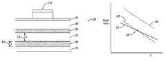
- the laser 200includes a substrate 212 with various layers arranged over the substrate 212 .
- an n-type semiconductor layer 210is arranged over the substrate 212 and the active region 204 is arranged over the semiconductor layer 210 .
- a p type semiconductor layer 208is arranged or formed over the active region 204 .
- the laser 200may be a DFB or a DBR laser, for example, and the laser 200 may also include a grating 206 . After the grating 206 is etched and defined, InP or other suitable material may be regrown and the laser is then fabricated using a standard ridge waveguide process. The grating 206 serves as the etch stop layer during the ridge waveguide process.
- the active region 204is effectively located at a pn junction.
- the active region 204includes a multi-quantum well structure.
- the material system of the quantum wellsis InGaAlAs in this example.
- the active region 204may include 6 quantum wells interleaved with 7 barrier layers, although one of skill in the art can appreciate that the invention may be implemented using more or fewer quantum wells and that other materials may be used in the quantum wells.
- Each quantum wellmay have a thickness on the order of 5 nm while the barrier layers may each have a thickness on the order of 8.5 nm.
- the barrier layers and/or the quantum wellsare tensile strained or compressive strained.
- the quantum wellsare compressive strained and the barrier layers and tensile strained.
- the photoluminescence of the active region 204 in this exampleis on the order of 1300 nm.
- One of skill in the artcan appreciate an active region having a photoluminescence that is greater or lower.
- FIG. 2Billustrates one embodiment of an active region 204 .
- the active region 204may also include graded index separate confinement heterostructure (GRINSCH) layers 222 , 226 .
- the GRINSCH layers 222 , 26sandwich the multi-quantum well structure 224 and are each on the order of 120 nanometers thick.
- the bandgapramps down from 960 nanometers to 850 nanometers moving away from the multi-quantum well structure 116 .
- Each GRINSCH layer 222 , 226is followed by a layer of InAlAs 220 , 228 that is 50 to 100 nanometers thick.
- the InAlAs layer 228would be formed on the layer 210 .
- the p-type semiconductor layer 208is formed on the other InAlAs layer 222 in this example.
- the p-type semiconductor layer 208is typically formed from InP.
- the grating layer 206is formed or grown on the layer 208 and is followed by a cap layer in which a ridge waveguide process is performed to form a ridge in the laser 100 .
- the grating layer 206acts as an etch stop.
- the metal contactmay then be deposited or formed after the ridge is formed in one embodiment.
- the laser 200also includes a waveguide layer 202 as illustrated in FIG. 2 .
- the waveguide layeris typically formed beneath the active region 204 .
- the waveguidemay be InGaAsP lattice matched to InP.
- the specific composition or other parameters of the waveguide layer 202can be altered as described below to improve the SMSR.
- FIGS. 3 and 4illustrate alternative embodiments of the invention.
- the waveguide layer 302 of the laser 300includes multiple layers. In one embodiment, the multiple layers in the waveguide layer 302 are distributed Bragg layers.
- FIG. 4illustrates a laser array 400 .
- a ridge waveguide structure 401is formed laterally adjacent to a ridge waveguide structure 403 .
- the structure 402includes a waveguide layer 402 that can optically couple with the active region 404 of the structure 403 .
- the waveguide layer 402is located sufficiently near the active region 403 for optical coupling to occur.
- the waveguide layer 218has a thickness 218 (t).
- t0 or when the waveguide layer 202 is not present, and for typical width values of the mesa 214 , the laser 200 may support a second order mode that can lead to the SMSR failure previously described.
- the second order modecouples with the waveguide layer 202 .
- the waveguide layermay have a thickness of about 115 nanometers and have a photoluminescence peak of about 1200 nanometers.
- the waveguide layer 202is a planar waveguide in this example and the second order mode is effectively coupled into the waveguide layer 202 .
- the optical confinement of the second order modeis reduced from its value when the thickness 218 equals zero.
- the confinement of the primary modeis not affected because the phase velocity of the waveguide layer is further away from the phase velocity of the primary mode. Thus, the optical confinement of the primary mode is not affected.
- FIG. 5Aplots the modal index (phase velocity) of a mode of the waveguide structure as well as the modal index of the modes of the active region as a function of wavelength.
- the strength of coupling between the waveguide layer and the active region modescan be either wavelength dependent or wavelength independent.
- the waveguide layeris typically configured such that the modal index curve illustrated in FIG. 5A is approximately parallel to the curve of the active region. When the curve of the waveguide layer is substantially parallel to the curve of the active region, the optical coupling is wavelength independent.
- the curves 504 and 502correspond to the primary and secondary modes of the laser active region, respectively.
- the curve 512corresponds to a mode of the waveguide layer. Because the modal index curve of the secondary mode 502 and the modal index curve of the waveguide layer 512 are close together, the secondary mode of the active region strongly couples with the waveguide layer. At the point 508 , the strength of coupling is the strongest and the loss of confinement of the secondary mode is maximized at this point.
- the primary modedoes not strongly couple with the waveguide layer because its modal index, as represented by the curve 504 , is not well matched to the modal index of the waveguide layer 512 . This suggests that the optical confinement of the primary mode is not substantially reduced while the optical confinement of the second order mode is reduced.
- the primary mode and secondary modelase at different wavelengths, but the above conditions are satisfied over a larger wavelength range than the separation of the primary and secondary lasing wavelengths, which is typically 5 to 10 nm.
- FIG. 5Bplots the confinement of the primary and secondary mode to the active region.
- the distance 216 (D) in FIG. 2Ais 1.2 micrometers and the waveguide layer has a bandgap of 1200 nanometers.
- the curve 550corresponds to the optical confinement
- the curve 552corresponds to the optical confinement of the secondary mode
- the curve 554corresponds to the primary mode.
- the mode confinement of the secondary modeis essentially zero.
- the waveguide layerbegins to influence the primary mode.
- the waveguide layerpermits the active region to be effectively single mode well above the width limit of a conventional waveguide laser.
- parameters of the feedback layermay also be adjusted to impact the mode confinement.
- parametersinclude, but are not limited to, thickness of the waveguide layer, location of the waveguide layer with respect to the active region (thickness of the layer 106 , for example), material composition or formulation of the waveguide layer, refractive index of the waveguide layer, modal index of the waveguide layer, and any combination thereof.
- Another parametermay be the number and type of layers in the waveguide layer.
- the formulation of the active regioncan also be adjusted to impact the mode confinement and/or the material gain of the active region.
Landscapes
- Physics & Mathematics (AREA)
- Condensed Matter Physics & Semiconductors (AREA)
- General Physics & Mathematics (AREA)
- Electromagnetism (AREA)
- Optics & Photonics (AREA)
- Geometry (AREA)
- Semiconductor Lasers (AREA)
Abstract
Description
Claims (20)
Priority Applications (1)
| Application Number | Priority Date | Filing Date | Title |
|---|---|---|---|
| US11/780,315US7711016B2 (en) | 2004-06-30 | 2007-07-19 | Semiconductor laser with side mode suppression |
Applications Claiming Priority (2)
| Application Number | Priority Date | Filing Date | Title |
|---|---|---|---|
| US10/880,655US7649916B2 (en) | 2004-06-30 | 2004-06-30 | Semiconductor laser with side mode suppression |
| US11/780,315US7711016B2 (en) | 2004-06-30 | 2007-07-19 | Semiconductor laser with side mode suppression |
Related Parent Applications (1)
| Application Number | Title | Priority Date | Filing Date |
|---|---|---|---|
| US10/880,655DivisionUS7649916B2 (en) | 2004-06-30 | 2004-06-30 | Semiconductor laser with side mode suppression |
Publications (2)
| Publication Number | Publication Date |
|---|---|
| US20070263688A1 US20070263688A1 (en) | 2007-11-15 |
| US7711016B2true US7711016B2 (en) | 2010-05-04 |
Family
ID=35513874
Family Applications (2)
| Application Number | Title | Priority Date | Filing Date |
|---|---|---|---|
| US10/880,655Expired - LifetimeUS7649916B2 (en) | 2004-06-30 | 2004-06-30 | Semiconductor laser with side mode suppression |
| US11/780,315Expired - LifetimeUS7711016B2 (en) | 2004-06-30 | 2007-07-19 | Semiconductor laser with side mode suppression |
Family Applications Before (1)
| Application Number | Title | Priority Date | Filing Date |
|---|---|---|---|
| US10/880,655Expired - LifetimeUS7649916B2 (en) | 2004-06-30 | 2004-06-30 | Semiconductor laser with side mode suppression |
Country Status (4)
| Country | Link |
|---|---|
| US (2) | US7649916B2 (en) |
| EP (1) | EP1766739B1 (en) |
| CN (1) | CN101076928A (en) |
| WO (1) | WO2006004835A2 (en) |
Families Citing this family (4)
| Publication number | Priority date | Publication date | Assignee | Title |
|---|---|---|---|---|
| US7649916B2 (en)* | 2004-06-30 | 2010-01-19 | Finisar Corporation | Semiconductor laser with side mode suppression |
| CN101867148B (en)* | 2009-04-15 | 2012-05-23 | 中国科学院半导体研究所 | FP (Fabry-Perot) cavity laser with reflecting surfaces of photonic crystals and vertical emergent surface |
| US20130114634A1 (en)* | 2011-11-09 | 2013-05-09 | Dmitri Vladislavovich Kuksenkov | DBR Laser Diode With Periodically Modulated Grating Phase |
| TWI766008B (en)* | 2017-06-15 | 2022-06-01 | 日商索尼半導體解決方案公司 | Surface Emitting Semiconductor Laser and Sensing Module |
Citations (32)
| Publication number | Priority date | Publication date | Assignee | Title |
|---|---|---|---|---|
| US3740661A (en) | 1969-06-06 | 1973-06-19 | Bell Telephone Labor Inc | Minor lobe suppression in semiconductor injection lasers |
| US3838359A (en) | 1973-11-23 | 1974-09-24 | Bell Telephone Labor Inc | Gain asymmetry in heterostructure junction lasers operating in a fundamental transverse mode |
| US3980392A (en)* | 1974-05-02 | 1976-09-14 | Siemens Aktiengesellschaft | Mode transducer for optical wave guides |
| US4077019A (en)* | 1976-01-05 | 1978-02-28 | Xerox Corporation | Transverse mode control in double-heterostructure lasers utilizing substrate loss |
| US4340967A (en) | 1980-06-02 | 1982-07-20 | Bell Telephone Laboratories, Incorporated | Semiconductor lasers with stable higher-order modes parallel to the junction plane |
| JPS61137388A (en) | 1984-12-10 | 1986-06-25 | Matsushita Electric Ind Co Ltd | semiconductor laser |
| US4701009A (en)* | 1985-02-04 | 1987-10-20 | Hughes Aircraft Company | Spectral filter for integrated optics |
| EP0285104A2 (en) | 1987-03-30 | 1988-10-05 | Sony Corporation | Distributed feedback semiconductor laser |
| US4833687A (en) | 1985-12-18 | 1989-05-23 | Sony Corporation | Distributed feedback semiconductor laser |
| US4990989A (en) | 1982-03-19 | 1991-02-05 | At&T Bell Laboratories | Restricted contact planar photodiode |
| US5208864A (en) | 1989-03-10 | 1993-05-04 | Nippon Telegraph & Telephone Corporation | Method of detecting acoustic signal |
| US5373166A (en) | 1993-01-11 | 1994-12-13 | International Business Machines Corporation | Modulated strain heterostructure light emitting device |
| US5381434A (en) | 1993-03-30 | 1995-01-10 | Bell Communications Research, Inc. | High-temperature, uncooled diode laser |
| US5436759A (en) | 1994-06-14 | 1995-07-25 | The Regents Of The University Of California | Cross-talk free, low-noise optical amplifier |
| US5438585A (en) | 1994-05-31 | 1995-08-01 | University Of New Mexico | Unstable resonator semiconductor laser |
| US5528616A (en)* | 1995-04-24 | 1996-06-18 | International Business Machines Corporation | Asymmetric dual waveguide laser |
| US5539759A (en)* | 1994-10-04 | 1996-07-23 | Board Of Trustees Of The Leland Stanford Junior University | Single mode laser with a passive antiguide region |
| US5541979A (en) | 1994-03-08 | 1996-07-30 | Allen Telecom Group, Inc. | Cell extender with timing alignment for use in time division multiple-access and similar cellular telephone systems |
| US5559912A (en)* | 1995-09-15 | 1996-09-24 | International Business Machines Corporation | Wavelength-selective devices using silicon-on-insulator |
| US5936994A (en) | 1997-09-18 | 1999-08-10 | Northern Telecom Limited | Two-section complex coupled distributed feedback semiconductor laser with enhanced wavelength tuning range |
| US5960023A (en) | 1996-04-15 | 1999-09-28 | Sharp Kabushiki Kaisha | Distributed feedback semiconductor laser diode, method for producing the same, and exposure method therefor |
| US6282345B1 (en) | 1996-09-13 | 2001-08-28 | Siemens Aktiengesellschaft | Device for coupling waveguides to one another |
| US20020051615A1 (en) | 2000-07-14 | 2002-05-02 | Walpole James N. | Slab-coupled optical waveguide laser and amplifier |
| US20020061046A1 (en) | 2000-11-20 | 2002-05-23 | Tohru Takiguchi | Distributed feedback laser device and method for manufacturing the same |
| US20030026309A1 (en) | 2001-08-01 | 2003-02-06 | Fuji Photo Film Co., Ltd. | Process for producing semiconductor laser element including S-ARROW structure formed by etching through mask having pair of parallel openings |
| US20030147439A1 (en) | 2001-12-11 | 2003-08-07 | Photonami, Inc. | Phase shifted surface emitting DFB laser structures with gain or absorptive gratings |
| US20040062286A1 (en) | 2002-09-26 | 2004-04-01 | Photodigm, Inc. | Single mode grating-outcoupled surface emitting laser with broadband and narrow-band DBR reflectors |
| US6879751B2 (en)* | 2002-01-30 | 2005-04-12 | Sioptical, Inc. | Method and apparatus for altering the effective mode index of an optical waveguide |
| US6940883B2 (en) | 2000-03-28 | 2005-09-06 | The Provost, Fellows And Scholars Of The College Of The Holy And Undivided Trinity Of Queen Elizabeth, Near Dublin | Laser diode |
| US20060002441A1 (en) | 2004-06-30 | 2006-01-05 | Finisar Corporation | Semiconductor laser with side mode suppression |
| US20060187986A1 (en) | 2005-02-24 | 2006-08-24 | Ming-Yung Jow | Optical communication module and multi-mode distributed feedback laser diode |
| US7577327B2 (en)* | 2001-10-30 | 2009-08-18 | Hoya Corporation Usa | Optical junction apparatus and methods employing optical power transverse-transfer |
Family Cites Families (2)
| Publication number | Priority date | Publication date | Assignee | Title |
|---|---|---|---|---|
| US4269635A (en)* | 1977-12-28 | 1981-05-26 | Bell Telephone Laboratories, Incorporated | Strip buried heterostructure laser |
| CA1137605A (en)* | 1979-01-15 | 1982-12-14 | Donald R. Scifres | High output power laser |
- 2004
- 2004-06-30USUS10/880,655patent/US7649916B2/ennot_activeExpired - Lifetime
- 2005
- 2005-06-30CNCNA2005800214156Apatent/CN101076928A/enactivePending
- 2005-06-30WOPCT/US2005/023102patent/WO2006004835A2/ennot_activeApplication Discontinuation
- 2005-06-30EPEP05856164.8Apatent/EP1766739B1/ennot_activeExpired - Lifetime
- 2007
- 2007-07-19USUS11/780,315patent/US7711016B2/ennot_activeExpired - Lifetime
Patent Citations (32)
| Publication number | Priority date | Publication date | Assignee | Title |
|---|---|---|---|---|
| US3740661A (en) | 1969-06-06 | 1973-06-19 | Bell Telephone Labor Inc | Minor lobe suppression in semiconductor injection lasers |
| US3838359A (en) | 1973-11-23 | 1974-09-24 | Bell Telephone Labor Inc | Gain asymmetry in heterostructure junction lasers operating in a fundamental transverse mode |
| US3980392A (en)* | 1974-05-02 | 1976-09-14 | Siemens Aktiengesellschaft | Mode transducer for optical wave guides |
| US4077019A (en)* | 1976-01-05 | 1978-02-28 | Xerox Corporation | Transverse mode control in double-heterostructure lasers utilizing substrate loss |
| US4340967A (en) | 1980-06-02 | 1982-07-20 | Bell Telephone Laboratories, Incorporated | Semiconductor lasers with stable higher-order modes parallel to the junction plane |
| US4990989A (en) | 1982-03-19 | 1991-02-05 | At&T Bell Laboratories | Restricted contact planar photodiode |
| JPS61137388A (en) | 1984-12-10 | 1986-06-25 | Matsushita Electric Ind Co Ltd | semiconductor laser |
| US4701009A (en)* | 1985-02-04 | 1987-10-20 | Hughes Aircraft Company | Spectral filter for integrated optics |
| US4833687A (en) | 1985-12-18 | 1989-05-23 | Sony Corporation | Distributed feedback semiconductor laser |
| EP0285104A2 (en) | 1987-03-30 | 1988-10-05 | Sony Corporation | Distributed feedback semiconductor laser |
| US5208864A (en) | 1989-03-10 | 1993-05-04 | Nippon Telegraph & Telephone Corporation | Method of detecting acoustic signal |
| US5373166A (en) | 1993-01-11 | 1994-12-13 | International Business Machines Corporation | Modulated strain heterostructure light emitting device |
| US5381434A (en) | 1993-03-30 | 1995-01-10 | Bell Communications Research, Inc. | High-temperature, uncooled diode laser |
| US5541979A (en) | 1994-03-08 | 1996-07-30 | Allen Telecom Group, Inc. | Cell extender with timing alignment for use in time division multiple-access and similar cellular telephone systems |
| US5438585A (en) | 1994-05-31 | 1995-08-01 | University Of New Mexico | Unstable resonator semiconductor laser |
| US5436759A (en) | 1994-06-14 | 1995-07-25 | The Regents Of The University Of California | Cross-talk free, low-noise optical amplifier |
| US5539759A (en)* | 1994-10-04 | 1996-07-23 | Board Of Trustees Of The Leland Stanford Junior University | Single mode laser with a passive antiguide region |
| US5528616A (en)* | 1995-04-24 | 1996-06-18 | International Business Machines Corporation | Asymmetric dual waveguide laser |
| US5559912A (en)* | 1995-09-15 | 1996-09-24 | International Business Machines Corporation | Wavelength-selective devices using silicon-on-insulator |
| US5960023A (en) | 1996-04-15 | 1999-09-28 | Sharp Kabushiki Kaisha | Distributed feedback semiconductor laser diode, method for producing the same, and exposure method therefor |
| US6282345B1 (en) | 1996-09-13 | 2001-08-28 | Siemens Aktiengesellschaft | Device for coupling waveguides to one another |
| US5936994A (en) | 1997-09-18 | 1999-08-10 | Northern Telecom Limited | Two-section complex coupled distributed feedback semiconductor laser with enhanced wavelength tuning range |
| US6940883B2 (en) | 2000-03-28 | 2005-09-06 | The Provost, Fellows And Scholars Of The College Of The Holy And Undivided Trinity Of Queen Elizabeth, Near Dublin | Laser diode |
| US20020051615A1 (en) | 2000-07-14 | 2002-05-02 | Walpole James N. | Slab-coupled optical waveguide laser and amplifier |
| US20020061046A1 (en) | 2000-11-20 | 2002-05-23 | Tohru Takiguchi | Distributed feedback laser device and method for manufacturing the same |
| US20030026309A1 (en) | 2001-08-01 | 2003-02-06 | Fuji Photo Film Co., Ltd. | Process for producing semiconductor laser element including S-ARROW structure formed by etching through mask having pair of parallel openings |
| US7577327B2 (en)* | 2001-10-30 | 2009-08-18 | Hoya Corporation Usa | Optical junction apparatus and methods employing optical power transverse-transfer |
| US20030147439A1 (en) | 2001-12-11 | 2003-08-07 | Photonami, Inc. | Phase shifted surface emitting DFB laser structures with gain or absorptive gratings |
| US6879751B2 (en)* | 2002-01-30 | 2005-04-12 | Sioptical, Inc. | Method and apparatus for altering the effective mode index of an optical waveguide |
| US20040062286A1 (en) | 2002-09-26 | 2004-04-01 | Photodigm, Inc. | Single mode grating-outcoupled surface emitting laser with broadband and narrow-band DBR reflectors |
| US20060002441A1 (en) | 2004-06-30 | 2006-01-05 | Finisar Corporation | Semiconductor laser with side mode suppression |
| US20060187986A1 (en) | 2005-02-24 | 2006-08-24 | Ming-Yung Jow | Optical communication module and multi-mode distributed feedback laser diode |
Non-Patent Citations (9)
| Title |
|---|
| Born, Max, et al., Principles of optics-Electromagnetic theory of propagation, interference and diffraction of light, Cambridge University Press, Seventh (Expanded) Edition 1999, pp. 16-19. |
| European Patent Application No. 05 85 6164.8, Supplementary European Search Report, mailed Dec. 16, 2009, 2 pages. |
| Takemoto, A., et al, 1.3 mum Distributed Feedback Laser Diode with a Grating Accurately Controlled by a New Fabrication Technique, IEEE, Journal of Lightwave Technology, vol. 7, No. 12, Dec. 1989, pp. 2072-2077. |
| Takemoto, A., et al, 1.3 μm Distributed Feedback Laser Diode with a Grating Accurately Controlled by a New Fabrication Technique, IEEE, Journal of Lightwave Technology, vol. 7, No. 12, Dec. 1989, pp. 2072-2077. |
| U.S. Appl. No. 10/880,655, filed Jul. 31, 2008, Office Action. |
| U.S. Appl. No. 10/880,655, filed Jun. 8, 2006, Office Action. |
| U.S. Appl. No. 10/880,655, filed Mar. 17, 2008, Restriction Requirement. |
| U.S. Appl. No. 10/880,655, filed May 30, 2006, Office Action. |
| U.S. Appl. No. 10/880,655, filed Oct. 3, 2006, Office Action. |
Also Published As
| Publication number | Publication date |
|---|---|
| EP1766739A4 (en) | 2010-01-27 |
| WO2006004835A2 (en) | 2006-01-12 |
| US20070263688A1 (en) | 2007-11-15 |
| CN101076928A (en) | 2007-11-21 |
| US7649916B2 (en) | 2010-01-19 |
| EP1766739B1 (en) | 2017-12-20 |
| EP1766739A2 (en) | 2007-03-28 |
| WO2006004835A3 (en) | 2007-08-02 |
| US20060002441A1 (en) | 2006-01-05 |
Similar Documents
| Publication | Publication Date | Title |
|---|---|---|
| JP5717726B2 (en) | DFB laser diode with lateral coupling for high output power | |
| US6580740B2 (en) | Semiconductor laser device having selective absorption qualities | |
| US20050053112A1 (en) | Surface emitting dfb laser structures for broadband communication systems and array of same | |
| JP2001308451A (en) | Semiconductor light emitting device | |
| US7835415B2 (en) | Single longitudinal mode laser diode | |
| JP2009076942A (en) | Distributed-feedback semiconductor laser, distributed-feedback semiconductor laser array, and optical module | |
| US6472691B2 (en) | Distributed feedback semiconductor laser device | |
| US7711016B2 (en) | Semiconductor laser with side mode suppression | |
| US6782022B2 (en) | Semiconductor laser device having improved output power characteristics | |
| US20030047738A1 (en) | Semiconductor laser device having selective absorption qualities over a wide temperature range | |
| US6661828B2 (en) | Semiconductor laser device | |
| JP4243506B2 (en) | Semiconductor laser and optical module using the same | |
| US8189631B2 (en) | External resonator-type wavelength tunable laser device | |
| US20060045157A1 (en) | Semiconductor laser with expanded mode | |
| US20020105718A1 (en) | Optoelectronic device having a diffraction grating associated therewith and a method of manufacture therefor | |
| US6839377B2 (en) | Optoelectronic device having a fiber grating stabilized pump module with increased locking range and a method of manufacture therefor | |
| CA2321607A1 (en) | Gain-coupled distributed-feedback semiconductor laser device | |
| JP2003234541A (en) | Distributed feedback semiconductor laser device | |
| US20050226283A1 (en) | Single-mode semiconductor laser with integrated optical waveguide filter | |
| Joyner et al. | A multifrequency waveguide grating laser by selective area epitaxy | |
| JP2006203100A (en) | Semiconductor laser and light transmitter module | |
| KR100693632B1 (en) | Quantum Well Laser Diode with Broadband Gain | |
| JP2009016878A (en) | Semiconductor laser and optical module using the same | |
| US7286588B2 (en) | Semiconductor laser with grating structure for stabilizing the wavelength of optical radiation | |
| JP2009087956A (en) | External resonator type variable wavelength laser and semiconductor optical amplifier built into the same |
Legal Events
| Date | Code | Title | Description |
|---|---|---|---|
| AS | Assignment | Owner name:FINISAR CORPORATION, CALIFORNIA Free format text:ASSIGNMENT OF ASSIGNORS INTEREST;ASSIGNORS:RATOWSKY, RICHARD P.;VERMA, ASHISH K.;ENG, LARS;REEL/FRAME:019647/0455 Effective date:20040628 Owner name:FINISAR CORPORATION,CALIFORNIA Free format text:ASSIGNMENT OF ASSIGNORS INTEREST;ASSIGNORS:RATOWSKY, RICHARD P.;VERMA, ASHISH K.;ENG, LARS;REEL/FRAME:019647/0455 Effective date:20040628 | |
| STCF | Information on status: patent grant | Free format text:PATENTED CASE | |
| FPAY | Fee payment | Year of fee payment:4 | |
| MAFP | Maintenance fee payment | Free format text:PAYMENT OF MAINTENANCE FEE, 8TH YEAR, LARGE ENTITY (ORIGINAL EVENT CODE: M1552) Year of fee payment:8 | |
| AS | Assignment | Owner name:BANK OF AMERICA, N.A., AS ADMINISTRATIVE AGENT, NO Free format text:NOTICE OF GRANT OF SECURITY INTEREST IN PATENTS;ASSIGNORS:II-VI INCORPORATED;MARLOW INDUSTRIES, INC.;EPIWORKS, INC.;AND OTHERS;REEL/FRAME:050484/0204 Effective date:20190924 Owner name:BANK OF AMERICA, N.A., AS ADMINISTRATIVE AGENT, NORTH CAROLINA Free format text:NOTICE OF GRANT OF SECURITY INTEREST IN PATENTS;ASSIGNORS:II-VI INCORPORATED;MARLOW INDUSTRIES, INC.;EPIWORKS, INC.;AND OTHERS;REEL/FRAME:050484/0204 Effective date:20190924 | |
| AS | Assignment | Owner name:II-VI DELAWARE, INC., DELAWARE Free format text:ASSIGNMENT OF ASSIGNORS INTEREST;ASSIGNOR:FINISAR CORPORATION;REEL/FRAME:052286/0001 Effective date:20190924 | |
| MAFP | Maintenance fee payment | Free format text:PAYMENT OF MAINTENANCE FEE, 12TH YEAR, LARGE ENTITY (ORIGINAL EVENT CODE: M1553); ENTITY STATUS OF PATENT OWNER: LARGE ENTITY Year of fee payment:12 | |
| AS | Assignment | Owner name:JPMORGAN CHASE BANK, N.A., AS COLLATERAL AGENT, NEW YORK Free format text:SECURITY INTEREST;ASSIGNORS:II-VI INCORPORATED;II-VI DELAWARE, INC.;M CUBED TECHNOLOGIES, INC.;AND OTHERS;REEL/FRAME:060562/0254 Effective date:20220701 | |
| AS | Assignment | Owner name:PHOTOP TECHNOLOGIES, INC., CALIFORNIA Free format text:PATENT RELEASE AND REASSIGNMENT;ASSIGNOR:BANK OF AMERICA, N.A., AS ADMINISTRATIVE AGENT;REEL/FRAME:060574/0001 Effective date:20220701 Owner name:II-VI OPTOELECTRONIC DEVICES, INC., NEW JERSEY Free format text:PATENT RELEASE AND REASSIGNMENT;ASSIGNOR:BANK OF AMERICA, N.A., AS ADMINISTRATIVE AGENT;REEL/FRAME:060574/0001 Effective date:20220701 Owner name:II-VI DELAWARE, INC., PENNSYLVANIA Free format text:PATENT RELEASE AND REASSIGNMENT;ASSIGNOR:BANK OF AMERICA, N.A., AS ADMINISTRATIVE AGENT;REEL/FRAME:060574/0001 Effective date:20220701 Owner name:II-VI PHOTONICS (US), INC., MASSACHUSETTS Free format text:PATENT RELEASE AND REASSIGNMENT;ASSIGNOR:BANK OF AMERICA, N.A., AS ADMINISTRATIVE AGENT;REEL/FRAME:060574/0001 Effective date:20220701 Owner name:M CUBED TECHNOLOGIES, INC., CONNECTICUT Free format text:PATENT RELEASE AND REASSIGNMENT;ASSIGNOR:BANK OF AMERICA, N.A., AS ADMINISTRATIVE AGENT;REEL/FRAME:060574/0001 Effective date:20220701 Owner name:II-VI OPTICAL SYSTEMS, INC., CALIFORNIA Free format text:PATENT RELEASE AND REASSIGNMENT;ASSIGNOR:BANK OF AMERICA, N.A., AS ADMINISTRATIVE AGENT;REEL/FRAME:060574/0001 Effective date:20220701 Owner name:FINISAR CORPORATION, CALIFORNIA Free format text:PATENT RELEASE AND REASSIGNMENT;ASSIGNOR:BANK OF AMERICA, N.A., AS ADMINISTRATIVE AGENT;REEL/FRAME:060574/0001 Effective date:20220701 Owner name:OPTIUM CORPORATION, CALIFORNIA Free format text:PATENT RELEASE AND REASSIGNMENT;ASSIGNOR:BANK OF AMERICA, N.A., AS ADMINISTRATIVE AGENT;REEL/FRAME:060574/0001 Effective date:20220701 Owner name:COADNA PHOTONICS, INC., PENNSYLVANIA Free format text:PATENT RELEASE AND REASSIGNMENT;ASSIGNOR:BANK OF AMERICA, N.A., AS ADMINISTRATIVE AGENT;REEL/FRAME:060574/0001 Effective date:20220701 Owner name:KAILIGHT PHOTONICS, INC., CALIFORNIA Free format text:PATENT RELEASE AND REASSIGNMENT;ASSIGNOR:BANK OF AMERICA, N.A., AS ADMINISTRATIVE AGENT;REEL/FRAME:060574/0001 Effective date:20220701 Owner name:LIGHTSMYTH TECHNOLOGIES, INC., OREGON Free format text:PATENT RELEASE AND REASSIGNMENT;ASSIGNOR:BANK OF AMERICA, N.A., AS ADMINISTRATIVE AGENT;REEL/FRAME:060574/0001 Effective date:20220701 Owner name:EPIWORKS, INC., ILLINOIS Free format text:PATENT RELEASE AND REASSIGNMENT;ASSIGNOR:BANK OF AMERICA, N.A., AS ADMINISTRATIVE AGENT;REEL/FRAME:060574/0001 Effective date:20220701 Owner name:MARLOW INDUSTRIES, INC., TEXAS Free format text:PATENT RELEASE AND REASSIGNMENT;ASSIGNOR:BANK OF AMERICA, N.A., AS ADMINISTRATIVE AGENT;REEL/FRAME:060574/0001 Effective date:20220701 Owner name:II-VI INCORPORATED, PENNSYLVANIA Free format text:PATENT RELEASE AND REASSIGNMENT;ASSIGNOR:BANK OF AMERICA, N.A., AS ADMINISTRATIVE AGENT;REEL/FRAME:060574/0001 Effective date:20220701 |