US7710629B2 - System and method for display device with reinforcing substance - Google Patents
System and method for display device with reinforcing substanceDownload PDFInfo
- Publication number
- US7710629B2 US7710629B2US11/144,305US14430505AUS7710629B2US 7710629 B2US7710629 B2US 7710629B2US 14430505 AUS14430505 AUS 14430505AUS 7710629 B2US7710629 B2US 7710629B2
- Authority
- US
- United States
- Prior art keywords
- backplate
- desiccant
- display device
- reinforcing substance
- reinforcing
- Prior art date
- Legal status (The legal status is an assumption and is not a legal conclusion. Google has not performed a legal analysis and makes no representation as to the accuracy of the status listed.)
- Expired - Fee Related, expires
Links
- 239000000126substanceSubstances0.000titleclaimsabstractdescription140
- 230000003014reinforcing effectEffects0.000titleclaimsabstractdescription133
- 238000000034methodMethods0.000titleclaimsabstractdescription30
- 239000002274desiccantSubstances0.000claimsabstractdescription228
- 239000000758substrateSubstances0.000claimsabstractdescription48
- XLYOFNOQVPJJNP-UHFFFAOYSA-NwaterSubstancesOXLYOFNOQVPJJNP-UHFFFAOYSA-N0.000claimsdescription68
- 230000008569processEffects0.000claimsdescription15
- 239000010457zeoliteSubstances0.000claimsdescription14
- 238000004519manufacturing processMethods0.000claimsdescription13
- 230000004888barrier functionEffects0.000claimsdescription12
- 239000000853adhesiveSubstances0.000claimsdescription7
- 230000001070adhesive effectEffects0.000claimsdescription7
- 238000007789sealingMethods0.000claimsdescription7
- VYPSYNLAJGMNEJ-UHFFFAOYSA-NSilicium dioxideChemical compoundO=[Si]=OVYPSYNLAJGMNEJ-UHFFFAOYSA-N0.000claimsdescription6
- 238000010521absorption reactionMethods0.000claimsdescription6
- 239000000292calcium oxideSubstances0.000claimsdescription6
- ODINCKMPIJJUCX-UHFFFAOYSA-Ncalcium oxideInorganic materials[Ca]=OODINCKMPIJJUCX-UHFFFAOYSA-N0.000claimsdescription6
- 239000000741silica gelSubstances0.000claimsdescription6
- 229910002027silica gelInorganic materials0.000claimsdescription6
- 239000007787solidSubstances0.000claimsdescription6
- 239000003463adsorbentSubstances0.000claimsdescription4
- BRPQOXSCLDDYGP-UHFFFAOYSA-Ncalcium oxideChemical compound[O-2].[Ca+2]BRPQOXSCLDDYGP-UHFFFAOYSA-N0.000claimsdescription4
- OSGAYBCDTDRGGQ-UHFFFAOYSA-Lcalcium sulfateChemical compound[Ca+2].[O-]S([O-])(=O)=OOSGAYBCDTDRGGQ-UHFFFAOYSA-L0.000claimsdescription4
- 238000011049fillingMethods0.000claimsdescription3
- 239000002808molecular sieveSubstances0.000claimsdescription3
- URGAHOPLAPQHLN-UHFFFAOYSA-Nsodium aluminosilicateChemical compound[Na+].[Al+3].[O-][Si]([O-])=O.[O-][Si]([O-])=OURGAHOPLAPQHLN-UHFFFAOYSA-N0.000claimsdescription3
- 239000011248coating agentSubstances0.000claimsdescription2
- 238000000576coating methodMethods0.000claimsdescription2
- 239000000376reactantSubstances0.000claimsdescription2
- 229920001600hydrophobic polymerPolymers0.000claims1
- 238000004806packaging method and processMethods0.000abstractdescription10
- 239000000463materialSubstances0.000description59
- 230000002035prolonged effectEffects0.000description27
- 239000011521glassSubstances0.000description18
- 239000000565sealantSubstances0.000description17
- 229910021536ZeoliteInorganic materials0.000description11
- HNPSIPDUKPIQMN-UHFFFAOYSA-Ndioxosilane;oxo(oxoalumanyloxy)alumaneChemical compoundO=[Si]=O.O=[Al]O[Al]=OHNPSIPDUKPIQMN-UHFFFAOYSA-N0.000description11
- 239000012528membraneSubstances0.000description11
- 238000010586diagramMethods0.000description8
- 229920000573polyethylenePolymers0.000description8
- 239000004593EpoxySubstances0.000description7
- 230000008901benefitEffects0.000description7
- -1e.g.Substances0.000description7
- 239000010408filmSubstances0.000description7
- 229910052751metalInorganic materials0.000description7
- 239000002184metalSubstances0.000description7
- 239000000203mixtureSubstances0.000description7
- 229920003023plasticPolymers0.000description7
- 239000004033plasticSubstances0.000description7
- 239000005361soda-lime glassSubstances0.000description7
- 150000001875compoundsChemical class0.000description6
- 238000001035dryingMethods0.000description6
- 239000011888foilSubstances0.000description6
- 229920000642polymerPolymers0.000description6
- 239000004698PolyethyleneSubstances0.000description5
- 230000003750conditioning effectEffects0.000description5
- 238000013461designMethods0.000description5
- 238000005516engineering processMethods0.000description5
- 238000010438heat treatmentMethods0.000description5
- 230000003287optical effectEffects0.000description5
- 238000000151depositionMethods0.000description4
- 238000005530etchingMethods0.000description4
- 230000004584weight gainEffects0.000description4
- 235000019786weight gainNutrition0.000description4
- 229920001328Polyvinylidene chloridePolymers0.000description3
- 229910052782aluminiumInorganic materials0.000description3
- XAGFODPZIPBFFR-UHFFFAOYSA-NaluminiumChemical compound[Al]XAGFODPZIPBFFR-UHFFFAOYSA-N0.000description3
- 230000005540biological transmissionEffects0.000description3
- 239000003990capacitorSubstances0.000description3
- 230000001413cellular effectEffects0.000description3
- 230000001419dependent effectEffects0.000description3
- 230000004907fluxEffects0.000description3
- 230000033001locomotionEffects0.000description3
- 238000012858packaging processMethods0.000description3
- 239000005033polyvinylidene chlorideSubstances0.000description3
- 239000000047productSubstances0.000description3
- 230000002787reinforcementEffects0.000description3
- 239000012779reinforcing materialSubstances0.000description3
- IJGRMHOSHXDMSA-UHFFFAOYSA-NAtomic nitrogenChemical compoundN#NIJGRMHOSHXDMSA-UHFFFAOYSA-N0.000description2
- 229920000298CellophanePolymers0.000description2
- VYZAMTAEIAYCRO-UHFFFAOYSA-NChromiumChemical compound[Cr]VYZAMTAEIAYCRO-UHFFFAOYSA-N0.000description2
- 229920002367PolyisobutenePolymers0.000description2
- 238000003491arrayMethods0.000description2
- 239000012298atmosphereSubstances0.000description2
- 229920002678cellulosePolymers0.000description2
- 239000001913celluloseSubstances0.000description2
- 239000000919ceramicSubstances0.000description2
- 230000008859changeEffects0.000description2
- 230000008021depositionEffects0.000description2
- 239000003292glueSubstances0.000description2
- 239000011261inert gasSubstances0.000description2
- 239000004800polyvinyl chlorideSubstances0.000description2
- 229920000915polyvinyl chloridePolymers0.000description2
- 239000000843powderSubstances0.000description2
- 230000009467reductionEffects0.000description2
- 229920006395saturated elastomerPolymers0.000description2
- 238000003892spreadingMethods0.000description2
- 230000007480spreadingEffects0.000description2
- 238000003860storageMethods0.000description2
- 238000012360testing methodMethods0.000description2
- 239000010409thin filmSubstances0.000description2
- IRLPACMLTUPBCL-KQYNXXCUSA-N5'-adenylyl sulfateChemical compoundC1=NC=2C(N)=NC=NC=2N1[C@@H]1O[C@H](COP(O)(=O)OS(O)(=O)=O)[C@@H](O)[C@H]1OIRLPACMLTUPBCL-KQYNXXCUSA-N0.000description1
- 208000036119FrailtyDiseases0.000description1
- HBBGRARXTFLTSG-UHFFFAOYSA-NLithium ionChemical compound[Li+]HBBGRARXTFLTSG-UHFFFAOYSA-N0.000description1
- 239000000020NitrocelluloseSubstances0.000description1
- 239000004775TyvekSubstances0.000description1
- 229920000690TyvekPolymers0.000description1
- FJWGYAHXMCUOOM-QHOUIDNNSA-N[(2s,3r,4s,5r,6r)-2-[(2r,3r,4s,5r,6s)-4,5-dinitrooxy-2-(nitrooxymethyl)-6-[(2r,3r,4s,5r,6s)-4,5,6-trinitrooxy-2-(nitrooxymethyl)oxan-3-yl]oxyoxan-3-yl]oxy-3,5-dinitrooxy-6-(nitrooxymethyl)oxan-4-yl] nitrateChemical compoundO([C@@H]1O[C@@H]([C@H]([C@H](O[N+]([O-])=O)[C@H]1O[N+]([O-])=O)O[C@H]1[C@@H]([C@@H](O[N+]([O-])=O)[C@H](O[N+]([O-])=O)[C@@H](CO[N+]([O-])=O)O1)O[N+]([O-])=O)CO[N+](=O)[O-])[C@@H]1[C@@H](CO[N+]([O-])=O)O[C@@H](O[N+]([O-])=O)[C@H](O[N+]([O-])=O)[C@H]1O[N+]([O-])=OFJWGYAHXMCUOOM-QHOUIDNNSA-N0.000description1
- 239000006096absorbing agentSubstances0.000description1
- 239000000654additiveSubstances0.000description1
- 230000000996additive effectEffects0.000description1
- 230000002411adverseEffects0.000description1
- 229910021417amorphous siliconInorganic materials0.000description1
- 238000004458analytical methodMethods0.000description1
- 238000013459approachMethods0.000description1
- 206010003549astheniaDiseases0.000description1
- 238000009638autodisplayMethods0.000description1
- 230000009286beneficial effectEffects0.000description1
- XIWFQDBQMCDYJT-UHFFFAOYSA-Mbenzyl-dimethyl-tridecylazanium;chlorideChemical compound[Cl-].CCCCCCCCCCCCC[N+](C)(C)CC1=CC=CC=C1XIWFQDBQMCDYJT-UHFFFAOYSA-M0.000description1
- 239000011230binding agentSubstances0.000description1
- 229920005549butyl rubberPolymers0.000description1
- OJIJEKBXJYRIBZ-UHFFFAOYSA-Ncadmium nickelChemical compound[Ni].[Cd]OJIJEKBXJYRIBZ-UHFFFAOYSA-N0.000description1
- 230000015556catabolic processEffects0.000description1
- 230000005465channelingEffects0.000description1
- 239000003795chemical substances by applicationSubstances0.000description1
- 229910052804chromiumInorganic materials0.000description1
- 239000011651chromiumSubstances0.000description1
- GVPFVAHMJGGAJG-UHFFFAOYSA-Lcobalt dichlorideChemical compound[Cl-].[Cl-].[Co+2]GVPFVAHMJGGAJG-UHFFFAOYSA-L0.000description1
- 239000003086colorantSubstances0.000description1
- 230000001010compromised effectEffects0.000description1
- 238000011109contaminationMethods0.000description1
- 238000001816coolingMethods0.000description1
- 238000006731degradation reactionMethods0.000description1
- 239000010432diamondSubstances0.000description1
- 239000003989dielectric materialSubstances0.000description1
- 230000009977dual effectEffects0.000description1
- 229920001971elastomerPolymers0.000description1
- 238000004146energy storageMethods0.000description1
- 230000007613environmental effectEffects0.000description1
- 125000003700epoxy groupChemical group0.000description1
- 230000001747exhibiting effectEffects0.000description1
- 239000012467final productSubstances0.000description1
- 239000012634fragmentSubstances0.000description1
- 239000000499gelSubstances0.000description1
- 239000011086glassineSubstances0.000description1
- 239000008187granular materialSubstances0.000description1
- 238000003384imaging methodMethods0.000description1
- AMGQUBHHOARCQH-UHFFFAOYSA-Nindium;oxotinChemical compound[In].[Sn]=OAMGQUBHHOARCQH-UHFFFAOYSA-N0.000description1
- 238000001746injection mouldingMethods0.000description1
- 239000002655kraft paperSubstances0.000description1
- 239000007788liquidSubstances0.000description1
- 229910001416lithium ionInorganic materials0.000description1
- 230000005923long-lasting effectEffects0.000description1
- 239000011159matrix materialSubstances0.000description1
- 239000007769metal materialSubstances0.000description1
- 238000005459micromachiningMethods0.000description1
- 238000002156mixingMethods0.000description1
- 229920001220nitrocellulosPolymers0.000description1
- 229910052757nitrogenInorganic materials0.000description1
- 238000005457optimizationMethods0.000description1
- 239000003973paintSubstances0.000description1
- 239000000123paperSubstances0.000description1
- 239000002245particleSubstances0.000description1
- 238000000059patterningMethods0.000description1
- 230000000149penetrating effectEffects0.000description1
- 230000035699permeabilityEffects0.000description1
- 239000012466permeateSubstances0.000description1
- 229920000647polyepoxidePolymers0.000description1
- 229920002635polyurethanePolymers0.000description1
- 239000004814polyurethaneSubstances0.000description1
- 238000002360preparation methodMethods0.000description1
- 238000012545processingMethods0.000description1
- 230000002040relaxant effectEffects0.000description1
- 239000011347resinSubstances0.000description1
- 229920005989resinPolymers0.000description1
- 239000005060rubberSubstances0.000description1
- 238000005488sandblastingMethods0.000description1
- 239000012812sealant materialSubstances0.000description1
- 239000004065semiconductorSubstances0.000description1
- 230000035945sensitivityEffects0.000description1
- 238000000926separation methodMethods0.000description1
- 229910052710siliconInorganic materials0.000description1
- 239000010703siliconSubstances0.000description1
- 229910000679solderInorganic materials0.000description1
- 238000001179sorption measurementMethods0.000description1
- 229920013744specialty plasticPolymers0.000description1
- 238000005728strengtheningMethods0.000description1
- 238000006467substitution reactionMethods0.000description1
- 238000007666vacuum formingMethods0.000description1
- 230000000007visual effectEffects0.000description1
- 238000001039wet etchingMethods0.000description1
- 210000000707wristAnatomy0.000description1
Images


Classifications
- B—PERFORMING OPERATIONS; TRANSPORTING
- B81—MICROSTRUCTURAL TECHNOLOGY
- B81B—MICROSTRUCTURAL DEVICES OR SYSTEMS, e.g. MICROMECHANICAL DEVICES
- B81B3/00—Devices comprising flexible or deformable elements, e.g. comprising elastic tongues or membranes
- B81B3/0064—Constitution or structural means for improving or controlling the physical properties of a device
- B81B3/0067—Mechanical properties
- B81B3/007—For controlling stiffness, e.g. ribs
- H—ELECTRICITY
- H04—ELECTRIC COMMUNICATION TECHNIQUE
- H04N—PICTORIAL COMMUNICATION, e.g. TELEVISION
- H04N5/00—Details of television systems
- H04N5/64—Constructional details of receivers, e.g. cabinets or dust covers
- B—PERFORMING OPERATIONS; TRANSPORTING
- B81—MICROSTRUCTURAL TECHNOLOGY
- B81B—MICROSTRUCTURAL DEVICES OR SYSTEMS, e.g. MICROMECHANICAL DEVICES
- B81B7/00—Microstructural systems; Auxiliary parts of microstructural devices or systems
- B81B7/0032—Packages or encapsulation
- B81B7/0035—Packages or encapsulation for maintaining a controlled atmosphere inside of the chamber containing the MEMS
- B81B7/0038—Packages or encapsulation for maintaining a controlled atmosphere inside of the chamber containing the MEMS using materials for controlling the level of pressure, contaminants or moisture inside of the package, e.g. getters
- G—PHYSICS
- G02—OPTICS
- G02B—OPTICAL ELEMENTS, SYSTEMS OR APPARATUS
- G02B26/00—Optical devices or arrangements for the control of light using movable or deformable optical elements
- G02B26/001—Optical devices or arrangements for the control of light using movable or deformable optical elements based on interference in an adjustable optical cavity
- B—PERFORMING OPERATIONS; TRANSPORTING
- B81—MICROSTRUCTURAL TECHNOLOGY
- B81B—MICROSTRUCTURAL DEVICES OR SYSTEMS, e.g. MICROMECHANICAL DEVICES
- B81B2201/00—Specific applications of microelectromechanical systems
- B81B2201/04—Optical MEMS
- B81B2201/047—Optical MEMS not provided for in B81B2201/042 - B81B2201/045
- B—PERFORMING OPERATIONS; TRANSPORTING
- B81—MICROSTRUCTURAL TECHNOLOGY
- B81C—PROCESSES OR APPARATUS SPECIALLY ADAPTED FOR THE MANUFACTURE OR TREATMENT OF MICROSTRUCTURAL DEVICES OR SYSTEMS
- B81C2203/00—Forming microstructural systems
- B81C2203/01—Packaging MEMS
- B81C2203/0163—Reinforcing a cap, e.g. with ribs
Definitions
- the field of the inventionrelates to microelectromechanical systems (MEMS). More specifically, the field of the invention relates to interferometric modulators with a reinforcing substance, e.g., a desiccant.
- MEMSmicroelectromechanical systems
- Microelectromechanical systemsinclude micro mechanical elements, actuators, and electronics. Micromechanical elements may be created using deposition, etching, and or other micromachining processes that etch away parts of substrates and/or deposited material layers or that add layers to form electrical and electromechanical devices.
- One type of MEMS deviceis called an interferometric modulator.
- interferometric modulator or interferometric light modulatorrefers to a device that selectively absorbs and/or reflects light using the principles of optical interference.
- an interferometric modulatormay comprise a pair of conductive plates, one or both of which may be transparent and/or reflective in whole or part and capable of relative motion upon application of an appropriate electrical signal.
- one platemay comprise a stationary layer deposited on a substrate and the other plate may comprise a metallic membrane separated from the stationary layer by an air gap.
- the position of one plate in relation to anothercan change the optical interference of light incident on the interferometric modulator.
- Such deviceshave a wide range of applications, and it would be beneficial in the art to utilize and/or modify the characteristics of these types of devices so that their features can be exploited in improving existing products and creating new products that have not yet been developed.
- Some embodiments of the inventionare package structures for an interferometric modulator that include a reinforcing substance.
- the reinforcing substanceis a desiccant.
- the desiccantcan be molded or integrated the backplate in such a manner that it provides a structural support for the backplate.
- the amount and type of desiccantcan be designed to optimize the water removing function while minimizing the amount of material, or cost of material, placed with the device.
- the inventionis a display device package that comprises a transparent substrate, an interferometric modulator configured to modulate light transmitted through the transparent substrate, a backplate cover sealed to the transparent substrate to form a package so that the interferometric modulator is inside of the package, and a reinforcing substance in contact with the backplate cover.
- the reinforcing substanceis configured to provide structural support to the backplate cover.
- the inventionis a method of manufacturing a display device.
- the methodcomprises providing a transparent substrate that comprises an interferometric modulator configured to modulate light transmitted through the transparent substrate, providing a backplate cover configured to mount to the transparent substrate, and applying a reinforcing substance to the backplate cover.
- the reinforcing substanceis configured to provide structural support to the backplate and is also a desiccant.
- the methodfurther comprises sealing the backplate cover to the transparent substrate.
- the inventionis a display device.
- the display devicecomprises a transparent substrate that comprises an interferometric modulator configured to modulate light transmitted through the transparent substrate, a backplate cover sealed to the transparent substrate to form a package so that the interferometric modulator is inside the package, and a prolonged-acting desiccant associated with the backplate cover.
- the prolonged-acting desiccanthas a half-life for absorbing water of not less than 10 hours.
- the inventionis a device that comprises an interferometric modulator, a backplate cover sealed to a transparent substrate to form a package so that the interferometric modulator is inside the package, and a reinforcing substance applied to an internal side of the backplate cover.
- the reinforcing substanceis configured to provide structural support to the backplate cover and is a desiccant.
- the inventionis a display device package that comprises a transparent substrate, an interferometric modulator configured to modulate light transmitted through the transparent substrate, a backplate cover sealed to the transparent substrate to form a package so that the interferometric modulator is inside the package, and a means for reinforcing the backplate cover.
- the inventionis a display device created by applying a reinforcing substance to a backplate cover, allowing the reinforcing substance to dry, and sealing a transparent substrate comprising an interferometric modulator to the backplate cover.
- the reinforcing substanceis a desiccant.
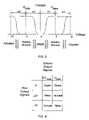
- FIG. 1is an isometric view depicting a portion of one embodiment of an interferometric modulator display in which a movable reflective layer of a first interferometric modulator is in a released position and a movable reflective layer of a second interferometric modulator is in an actuated position.
- FIG. 2is a system block diagram illustrating one embodiment of an electronic device incorporating a 3 ⁇ 3 interferometric modulator display.
- FIG. 3is a diagram of movable mirror position versus applied voltage for one exemplary embodiment of an interferometric modulator of FIG. 1 .
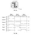
- FIG. 4is an illustration of a set of row and column voltages that may be used to drive an interferometric modulator display.
- FIGS. 5A and 5Billustrate one exemplary timing diagram for row and column signals that may be used to write a frame of display data to the 3 ⁇ 3 interferometric modulator display of FIG. 2 .
- FIG. 6Ais a system block diagram illustrating an embodiment of a display device.
- FIG. 6Bis a system block diagram illustrating some of the components of an embodiment of a display device.
- FIG. 7Ais a cross section of the device of FIG. 1 .
- FIG. 7Bis a cross section of an alternative embodiment of an interferometric modulator.
- FIG. 7Cis a cross section of another alternative embodiment of an interferometric modulator.
- FIG. 8schematically illustrates a front view of one embodiment of a wireless telephone handset having an electronic display.
- FIG. 9schematically illustrates a perspective view of one embodiment of an electronic display.
- FIG. 10schematically illustrates a cross-sectional view of one embodiment of an electronic display taken across the line 3 - 3 from FIG. 9 .
- FIG. 11schematically illustrates a first alternate embodiment of an electronic display taken across the line 3 - 3 from FIG. 9 .
- FIG. 12schematically illustrates several embodiments of how the reinforcing substance can be used to add support or increase the integrity of the backplate.
- FIG. 13schematically illustrates an alternative embodiment of how the reinforcing substance can add support to the backplate.
- FIG. 14Aschematically illustrates one embodiment of how a reinforcing substance can be configured.
- FIG. 14Bschematically illustrates another embodiment of how a reinforcing substance can be configured.
- FIG. 14Cschematically illustrates another embodiment of how a reinforcing substance can be configured.
- FIG. 14Dschematically illustrates another embodiment of how a reinforcing substance can be configured.
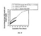
- FIG. 15Ais a graph depicting the rates of water absorption for HiCap2800TM desiccant, a prolonged acting desiccant.
- FIG. 15Bis a graph depicting the rates of water absorption for Bondline Zeolite desiccant, a fast acting desiccant.
- FIG. 16is a graph comparing the percent weight gain for ZeoliteTM and StayDry HiCapTM desiccants.
- the embodimentsmay be implemented in or associated with a variety of electronic devices such as, but not limited to, mobile telephones, wireless devices, personal data assistants (PDAs), hand-held or portable computers, GPS receivers/navigators, cameras, MP3 players, camcorders, game consoles, wrist watches, clocks, calculators, television monitors, flat panel displays, computer monitors, auto displays (e.g., odometer display, etc.), cockpit controls and/or displays, display of camera views (e.g., display of a rear view camera in a vehicle), electronic photographs, electronic billboards or signs, projectors, architectural structures, packaging, and aesthetic structures (e.g., display of images on a piece of jewelry).
- MEMS devices of similar structure to those described hereincan also be used in non-display applications such as in electronic switching devices.
- the inventionis a reinforcing substance on the surface of a backplate in a package of an interferometric modulator.
- the reinforcing aspect of the substancecan be achieved in a variety of ways.
- the reinforcing substratecan fill variations or imperfections in the backplate and thereby provide additional structural support.
- the reinforcing substancecan form a reinforcing structure in itself, which can add additional strength to the backplate. This can allow for thinner backplates to be used.
- the reinforcing substanceis a desiccant.
- the desiccantis a prolonged acting or long acting desiccant, which, while not necessarily absorbing large amounts of water immediately, is able to absorb water over a relatively prolonged period of time.
- the desiccantis covered by a barrier that reduces the amount of water that is exposed to the desiccant and thereby extends the effective lifetime of the desiccant.
- the desiccantis positioned selectively on the backplate to add support to weak points on the backplate, e.g., on the corners of the backplate. Methods of making and using these embodiments are also contemplated.
- FIG. 1One interferometric modulator display embodiment comprising an interferometric MEMS display element is illustrated in FIG. 1 .
- the pixelsare in either a bright or dark state.
- the display elementIn the bright (“on” or “open”) state, the display element reflects a large portion of incident visible light to a user.
- the dark (“off” or “closed”) stateWhen in the dark (“off” or “closed”) state, the display element reflects little incident visible light to the user.
- the light reflectance properties of the “on” and “off” statesmay be reversed.
- MEMS pixelscan be configured to reflect predominantly at selected colors, allowing for a color display in addition to black and white.
- FIG. 1is an isometric view depicting two adjacent pixels in a series of pixels of a visual display, wherein each pixel comprises a MEMS interferometric modulator.
- an interferometric modulator displaycomprises a row/column array of these interferometric modulators.
- Each interferometric modulatorincludes a pair of reflective layers positioned at a variable and controllable distance from each other to form a resonant optical cavity with at least one variable dimension.
- one of the reflective layersmay be moved between two positions. In the first position, referred to herein as the relaxed, the movable layer is positioned at a relatively large distance from a fixed partially reflective layer.
- the movable layerIn the second position, the movable layer is positioned more closely adjacent to the partially reflective layer. Incident light that reflects from the two layers interferes constructively or destructively depending on the position of the movable reflective layer, producing either an overall reflective or non-reflective state for each pixel.
- the depicted portion of the pixel array in FIG. 1includes two adjacent interferometric modulators 12 a and 12 b .
- a movable and highly reflective layer 14 ais illustrated in a relaxed position at a predetermined distance from a fixed partially reflective layer 16 a .
- the movable highly reflective layer 14 bis illustrated in an actuated position adjacent to the fixed partially reflective layer 16 b.
- the fixed layers 16 a , 16 bare electrically conductive, partially transparent and partially reflective, and may be fabricated, for example, by depositing one or more layers each of chromium and indium-tin-oxide onto a transparent substrate 20 .
- the layersare patterned into parallel strips, and may form row electrodes in a display device as described further below.
- the movable layers 14 a , 14 bmay be formed as a series of parallel strips of a deposited metal layer or layers (orthogonal to the row electrodes 16 a , 16 b ) deposited on top of posts 18 and an intervening sacrificial material deposited between the posts 18 .
- the deformable metal layers 14 a , 14 bare separated from the fixed metal layers by a defined gap 19 .
- a highly conductive and reflective materialsuch as aluminum may be used for the deformable layers, and these strips may form column electrodes in a display device.
- the cavity 19remains between the layers 14 a , 16 a and the deformable layer is in a mechanically relaxed state as illustrated by the pixel 12 a in FIG. 1 .
- the capacitor formed at the intersection of the row and column electrodes at the corresponding pixelbecomes charged, and electrostatic forces pull the electrodes together.
- the movable layeris deformed and is forced against the fixed layer (a dielectric material which is not illustrated in this Figure may be deposited on the fixed layer to prevent shorting and control the separation distance) as illustrated by the pixel 12 b on the right in FIG. 1 .
- the behavioris the same regardless of the polarity of the applied potential difference. In this way, row/column actuation that can control the reflective vs. non-reflective pixel states is analogous in many ways to that used in conventional LCD and other display technologies.
- FIGS. 2 through 5illustrate one exemplary process and system for using an array of interferometric modulators in a display application.
- FIG. 2is a system block diagram illustrating one embodiment of an electronic device that may incorporate aspects of the invention.
- the electronic deviceincludes a processor 21 which may be any general purpose single- or multi-chip microprocessor such as an ARM, Pentium®, Pentium II®, Pentium III®, Pentium IV®, Pentium® Pro, an 8051, a MIPS®, a Power PC®, an ALPHA®, or any special purpose microprocessor such as a digital signal processor, microcontroller, or a programmable gate array.
- the processor 21may be configured to execute one or more software modules.
- the processormay be configured to execute one or more software applications, including a web browser, a telephone application, an email program, or any other software application.
- the processor 21is also configured to communicate with an array controller 22 .
- the array controller 22includes a row driver circuit 24 and a column driver circuit 26 that provide signals to a display array or panel 30 .
- the cross section of the array illustrated in FIG. 1is shown by the lines 1 - 1 in FIG. 2 .
- the row/column actuation protocolmay take advantage of a hysteresis property of these devices illustrated in FIG. 3 . It may require, for example, a 10 volt potential difference to cause a movable layer to deform from the relaxed state to the actuated state. However, when the voltage is reduced from that value, the movable layer maintains its state as the voltage drops back below 10 volts.
- the movable layerdoes not relax completely until the voltage drops below 2 volts.
- There is thus a range of voltage, about 3 to 7 V in the example illustrated in FIG. 3where there exists a window of applied voltage within which the device is stable in either the relaxed or actuated state. This is referred to herein as the “hysteresis window” or “stability window.”
- hysteresis windowor “stability window.”
- the row/column actuation protocolcan be designed such that during row strobing, pixels in the strobed row that are to be actuated are exposed to a voltage difference of about 10 volts, and pixels that are to be relaxed are exposed to a voltage difference of close to zero volts. After the strobe, the pixels are exposed to a steady state voltage difference of about 5 volts such that they remain in whatever state the row strobe put them in. After being written, each pixel sees a potential difference within the “stability window” of 3-7 volts in this example. This feature makes the pixel design illustrated in FIG. 1 stable under the same applied voltage conditions in either an actuated or relaxed pre-existing state.
- each pixel of the interferometric modulatoris essentially a capacitor formed by the fixed and moving reflective layers, this stable state can be held at a voltage within the hysteresis window with almost no power dissipation. Essentially no current flows into the pixel if the applied potential is fixed.
- a display framemay be created by asserting the set of column electrodes in accordance with the desired set of actuated pixels in the first row.
- a row pulseis then applied to the row 1 electrode, actuating the pixels corresponding to the asserted column lines.
- the asserted set of column electrodesis then changed to correspond to the desired set of actuated pixels in the second row.
- a pulseis then applied to the row 2 electrode, actuating the appropriate pixels in row 2 in accordance with the asserted column electrodes.
- the row 1 pixelsare unaffected by the row 2 pulse, and remain in the state they were set to during the row 1 pulse. This may be repeated for the entire series of rows in a sequential fashion to produce the frame.
- the framesare refreshed and/or updated with new display data by continually repeating this process at some desired number of frames per second.
- protocols for driving row and column electrodes of pixel arrays to produce display framesare also well known and may be used in conjunction with the present invention.
- FIGS. 4 and 5illustrate one possible actuation protocol for creating a display frame on the 3 ⁇ 3 array of FIG. 2 .
- FIG. 4illustrates a possible set of column and row voltage levels that may be used for pixels exhibiting the hysteresis curves of FIG. 3 .
- actuating a pixelinvolves setting the appropriate column to ⁇ V bias , and the appropriate row to + ⁇ V, which may correspond to ⁇ 5 volts and +5 volts respectively Relaxing the pixel is accomplished by setting the appropriate column to +V bias , and the appropriate row to the same + ⁇ V, producing a zero volt potential difference across the pixel.
- the pixelsare stable in whatever state they were originally, in, regardless of whether the column is at +V bias , or ⁇ V bias .
- voltages of opposite polarity than those described abovecan be used, e.g., actuating a pixel can involve setting the appropriate column to +V bias , and the appropriate row to ⁇ V.
- releasing the pixelis accomplished by setting the appropriate column to ⁇ V bias , and the appropriate row to the same ⁇ V, producing a zero volt potential difference across the pixel.
- FIG. 5Bis a timing diagram showing a series of row and column signals applied to the 3 ⁇ 3 array of FIG. 2 which will result in the display arrangement illustrated in FIG. 5A , where actuated pixels are non-reflective.
- the pixelsPrior to writing the frame illustrated in FIG. 5A , the pixels can be in any state, and in this example, all the rows are at 0 volts, and all the columns are at +5 volts. With these applied voltages, all pixels are stable in their existing actuated or relaxed states.
- pixels (1,1), (1,2), (2,2), (3,2) and (3,3)are actuated.
- columns 1 and 2are set to ⁇ 5 volts
- column 3is set to +5 volts. This does not change the state of any pixels, because all the pixels remain in the 3-7 volt stability window.
- Row 1is then strobed with a pulse that goes from 0, up to 5 volts, and back to zero. This actuates the (1,1) and (1,2) pixels and relaxes the (1,3) pixel. No other pixels in the array are affected.
- column 2is set to ⁇ 5 volts
- columns 1 and 3are set to +5 volts.
- Row 3is similarly set by setting columns 2 and 3 to ⁇ 5 volts, and column 1 to +5 volts.
- the row 3 strobesets the row 3 pixels as shown in FIG. 5A .
- the row potentialsare zero, and the column potentials can remain at either +5 or ⁇ 5 volts, and the display is then stable in the arrangement of FIG. 5A . It will be appreciated that the same procedure can be employed for arrays of dozens or hundreds of rows and columns.
- FIGS. 6A and 6Bare system block diagrams illustrating an embodiment of a display device 40 .
- the display device 40can be, for example, a cellular or mobile telephone.
- the same components of display device 40 or slight variations thereofare also illustrative of various types of display devices such as televisions and portable media players.
- the display device 40includes a housing 41 , a display 30 , an antenna 43 , a speaker 44 , an input device 48 , and a microphone 46 .
- the housing 41is generally formed from any of a variety of manufacturing processes as are well known to those of skill in the art, including injection molding, and vacuum forming.
- the housing 41may be made from any of a variety of materials, including but not limited to plastic, metal, glass, rubber, and ceramic, or a combination thereof.
- the housing 41includes removable portions (not shown) that may be interchanged with other removable portions of different color, or containing different logos, pictures, or symbols.
- the display 30 of exemplary display device 40may be any of a variety of displays, including a bi-stable display, as described herein.
- the display 30includes a flat-panel display, such as plasma, EL, OLED, STN LCD, or TFT LCD as described above, or a non-flat-panel display, such as a CRT or other tube device, as is well known to those of skill in the art.
- the display 30includes an interferometric modulator display, as described herein.
- the components of one embodiment of exemplary display device 40are schematically illustrated in FIG. 6B .
- the illustrated exemplary display device 40includes a housing 41 and can include additional components at least partially enclosed therein.
- the exemplary display device 40includes a network interface 27 that includes an antenna 43 which is coupled to a transceiver 47 .
- the transceiver 47is connected to a processor 21 , which is connected to conditioning hardware 52 .
- the conditioning hardware 52may be configured to condition a signal (e.g. filter a signal).
- the conditioning hardware 52is connected to a speaker 44 and a microphone 46 .
- the processor 21is also connected to an input device 48 and a driver controller 29 .
- the driver controller 29is coupled to a frame buffer 28 , and to an array driver 22 , which in turn is coupled to a display array 30 .
- a power supply 50provides power to all components as required by the particular exemplary display device 40 design.
- the network interface 27includes the antenna 43 and the transceiver 47 so that the exemplary display device 40 can communicate with one ore more devices over a network. In one embodiment the network interface 27 may also have some processing capabilities to relieve requirements of the processor 21 .
- the antenna 43is any antenna known to those of skill in the art for transmitting and receiving signals. In one embodiment, the antenna transmits and receives RF signals according to the IEEE 802.11 standard, including IEEE 802.11(a), (b), or (g). In another embodiment, the antenna transmits and receives RF signals according to the BLUETOOTH standard. In the case of a cellular telephone, the antenna is designed to receive CDMA, GSM, AMPS or other known signals that are used to communicate within a wireless cell phone network.
- the transceiver 47pre-processes the signals received from the antenna 43 so that they may be received by and further manipulated by the processor 21 .
- the transceiver 47also processes signals received from the processor 21 so that they may be transmitted from the exemplary display device 40 via the antenna 43 .
- the transceiver 47can be replaced by a receiver.
- network interface 27can be replaced by an image source, which can store or generate image data to be sent to the processor 21 .
- the image sourcecan be a digital video disc (DVD) or a hard-disc drive that contains image data, or a software module that generates image data.
- Processor 21generally controls the overall operation of the exemplary display device 40 .
- the processor 21receives data, such as compressed image data from the network interface 27 or an image source, and processes the data into raw image data or into a format that is readily processed into raw image data.
- the processor 21then sends the processed data to the driver controller 29 or to frame buffer 28 for storage.
- Raw datatypically refers to the information that identifies the image characteristics at each location within an image. For example, such image characteristics can include color, saturation, and gray-scale level.
- the processor 21includes a microcontroller, CPU, or logic unit to control operation of the exemplary display device 40 .
- Conditioning hardware 52generally includes amplifiers and filters for transmitting signals to the speaker 44 , and for receiving signals from the microphone 46 .
- Conditioning hardware 52may be discrete components within the exemplary display device 40 , or may be incorporated within the processor 21 or other components.
- the driver controller 29takes the raw image data generated by the processor 21 either directly from the processor 21 or from the frame buffer 28 and reformats the raw image data appropriately for high speed transmission to the array driver 22 . Specifically, the driver controller 29 reformats the raw image data into a data flow having a raster-like format, such that it has a time order suitable for scanning across the display array 30 . Then the driver controller 29 sends the formatted information to the array driver 22 .
- a driver controller 29such as a LCD controller, is often associated with the system processor 21 as a stand-alone Integrated Circuit (IC), such controllers may be implemented in many ways. They may be embedded in the processor 21 as hardware, embedded in the processor 21 as software, or fully integrated in hardware with the array driver 22 .
- the array driver 22receives the formatted information from the driver controller 29 and reformats the video data into a parallel set of waveforms that are applied many times per second to the hundreds and sometimes thousands of leads coming from the display's x-y matrix of pixels.
- driver controller 29is a conventional display controller or a bi-stable display controller (e.g., an interferometric modulator controller).
- array driver 22is a conventional driver or a bi-stable display driver (e.g., an interferometric modulator display).
- a driver controller 29is integrated with the array driver 22 .
- display array 30is a typical display array or a bi-stable display array (e.g., a display including an array of interferometric modulators).
- the input device 48allows a user to control the operation of the exemplary display device 40 .
- input device 48includes a keypad, such as a QWERTY keyboard or a telephone keypad, a button, a switch, a touch-sensitive screen, a pressure- or heat-sensitive membrane.
- the microphone 46is an input device for the exemplary display device 40 . When the microphone 46 is used to input data to the device, voice commands may be provided by a user for controlling operations of the exemplary display device 40 .
- Power supply 50can include a variety of energy storage devices as are well known in the art.
- power supply 50is a rechargeable battery, such as a nickel-cadmium battery or a lithium ion battery.
- power supply 50is a renewable energy source, a capacitor, or a solar cell, including a plastic solar cell, and solar-cell paint.
- power supply 50is configured to receive power from a wall outlet.
- control programmabilityresides, as described above, in a driver controller which can be located in several places in the electronic display system. In some cases control programmability resides in the array driver 22 . Those of skill in the art will recognize that the above-described optimization may be implemented in any number of hardware and/or software components and in various configurations.
- FIGS. 7A-7Cillustrate three different embodiments of the moving mirror structure.
- FIG. 7Ais a cross section of the embodiment of FIG. 1 , where a strip of metal material 14 is deposited on orthogonally extending supports 18 .
- FIG. 7Bthe moveable reflective material 14 is attached to supports at the corners only, on tethers 32 .
- FIG. 7Cthe moveable reflective material 14 is suspended from a deformable layer 34 .
- This embodimenthas benefits because the structural design and materials used for the reflective material 14 can be optimized with respect to the optical properties, and the structural design and materials used for the deformable layer 34 can be optimized with respect to desired mechanical properties.
- FIG. 8illustrates a wireless telephone handset 110 having an electronic display 120 .
- the electronic display 120is displaying the telephone number “555-1212”.
- Electronic display 120can be any type of display including light emitting diode (LED), organic light emitting diode (OLED), or an interferometric modulator (IMOD) direct view electronic display.
- LEDlight emitting diode
- OLEDorganic light emitting diode
- IMODinterferometric modulator
- FIG. 10shows a perspective view of the display 120 from FIG. 9 .
- the display 120has a transparent front surface 125 , a sealant 128 , and a backplate 130 .
- the electronics for the particular display technologywithin the display can be the electronics for an LED, OLED or IMOD display.
- Interferometric displayswhich are based on MEMS (micro-electro-mechanical-systems) technology, are spatial light modulators that may be used in electronic display applications, such as a wireless telephone handset.
- Interferometric modulatorsmodulate light by controlling the self-interference of light that strikes a surface of the modulator.
- U.S. Pat. No. 5,835,255discloses one example of an interferometric modulator which is hereby incorporated by reference in its entirety.
- the size of the backplate 130can be miniaturized to allow for smaller display devices, this results in a thinner backplate which could be relatively weak. Additionally, some manufacturing processes can leave minor imperfections in the backplate, which may weaken the structure as well. Thus, stronger backplates to allow for smaller devices can be desirable. Additionally, it should be realized that each of the above display types are differentially sensitive to moisture. Thus it can be advantageous to provide a means for reducing the amount of moisture that may come in contact with the device.
- aspects of the inventionrelate to the manufacturing and packaging of electronic displays with a reinforcing substance.
- the reinforcing substanceis configured to add structural support to the package.
- the reinforcing substancecan also be configured to absorb water molecules that permeate the display packaging once it has been manufactured, e.g., it can be a desiccant.
- a desiccantmaintains a low humidity environment within the display package and prevents water vapor from adversely affecting the operation of the display electronics. This will be explained in further detail below.
- Interferometric modulatorstypically include a transparent substrate, such as glass, as well as moving parts that have a protected space in which to move.
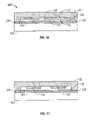
- a schematic of a basic package structure for an interferometric modulatoris illustrated in FIG. 10 , although it should be realized that the invention is not limited to packaging a particular type of display or the use of a particular substrate material, such as glass.
- a basic package structureincludes the transparent substrate 125 and the backplate cover or “cap” 130 . These components are held together by the sealant 128 , but provide a cavity 135 formed between these two components. Within the cavity 135 and adjacent the transparent substrate 125 is an interferometric modulator 140 .
- the cavity 135can also be provided by the use of a backplate glass that has a recessed cavity. Using a recessed cavity 135 allows the sealant material 128 to be relatively thin, and thus not be as subject to transmission of water vapor.
- An alternative package structureis shown in FIG. 11 .
- the transparent substrate 125can be any transparent substance capable of having display electronics, such as a thin film MEMS device built upon it. Such transparent substances include, but are not limited to, glass, plastic, and transparent polymers. Images are displayed through the substrate 125 , which serves as an imaging surface.
- the interferometric modulator arraymay comprise membrane modulators or modulators of the separable type. Examples of such devices are described in U.S. Pat. No. 5,835,255 to Miles.
- the backplate 130can be formed of any suitable material, such as glass, metal, foil, polymer, plastic, ceramic, or semiconductor materials (e.g., silicon).
- the interferometric modulator 140can be a membrane modulator or modulators of the separable type. Examples of such devices are described in U.S. Pat. No. 5,835,255 to Miles, hereby incorporated in its entirety by reference.
- the backplate 130can independently be strong enough so that the integrity of the packaging system is not compromised, either throughout the manufacture or throughout the use of the device.
- the dimensions, shape, composition, and other characteristics of the backplatecan be altered depending on the presence or absence of a reinforcing substance in the package.
- reinforcement of the packageallows for the manufacture of a relatively thin display.
- reinforcement of the packagemaintains a minimum bowing of the recessed glass to the order or 100-200 micron when moderate pressure is applied to the backplate.
- a backplatein which a reinforcing substance is to be used, can be thinner or may be insufficient to independently maintain the structural integrity of the packaging system.
- the reinforcing substancecan simply add additional strength to the system or other desired characteristics, such as a drying ability, or both characteristics.
- This backplate 130may also be referred to as a “backplane.” It will be understood that the terms “display,” “package structure,” and “package” can be used interchangeably, as used herein.
- the sealant or seal 128is typically provided to join the transparent substrate 125 and backplate 130 to form the package structure 120 .
- the sealant 128is typically a non-hermetic seal, such as a conventional epoxy-based adhesive.
- the sealant 128may be made from any polymer, or plastic composition.
- the sealant 128provides a hermetic seal that prevents water vapor and moisture from entering the cavity 135 .
- the seal 128can be a polyisobutylene (sometimes called butyl rubber, and other times PIB), o-rings, polyurethane, thin film metal weld, liquid spin-on glass, or solder, among other types of seals that can have a range of permeability of water vapor of about 0.2-4.7 g mm/m 2 kPa day.
- PIBpolyisobutylene
- o-ringssometimes called butyl rubber, and other times PIB
- polyurethanepolyurethane
- thin film metal weldthin film metal weld
- liquid spin-on glassor solder
- the cavity 135there is a cavity 135 between the backplate 130 and the substrate 125 .
- the moving parts of a MEMS devicesuch as the movable mirrors 14 a , 14 b of an interferometric modulator array described above, preferably have a protected space in which to move.
- the cavity 135can be provided by the use of a backplate 130 that has a recessed cavity.
- the reinforcing substancecan be selected from a variety of substances.
- the reinforcing substancecan be an epoxy, a desiccant, or some combination thereof.
- pastescan be prepared by mixing a CaO desiccant or Zeolite desiccant with a polymeric binder.
- An example of a desiccant pasteis the commercially available Cookson HiCap 2800TM desiccant paste. This paste can be screen printed or dispensed onto the backplate. It can have a thin sheet on the order of 50 microns for example, or various shapes and patterns, as described in more detail below.
- the pastecan be heated and activated after dispensing.
- Another type, a Zeolite based paste for examplecan be spread in a similar way, but may not require heating or activated after application.
- the reinforcing substanceprovides structural support to the package. This support can be due to, for example, the strength and integrity of the reinforcing substance, the shape of the reinforcing substance, its ability to interact with the backplate, or the position or location in which the reinforcing substance is placed. These options are discussed in more detail below.
- the integrity of the packagecan be improved through the filling of holes or crevices in the backplate.
- Some methods of manufacturing the backplateinvolve abrasive techniques that can over-etch or crack the backplate. These imperfections in the backplate can weaken the backplate and even provide possible routes through which water or other ambient substances can enter the device. While making a thicker backplate might overcome some of this problem, such a process may require more material and result in a larger device. However, it should be realized that even a thicker backplate may not solve the problem of backplane weakness and reduce the potential of having fracture points in the glass due to usage and temperature variations.
- any cracks in the glasscan propagate independent of whether the glass is thick (for example, > about 1.1 mm) or thin (for example, ⁇ about 0.7 mm). Additionally, throughout the manufacturing process, a crack could still occur in the backplate.
- a reinforcing substrate 148can be added to the backplate 130 that fills, e.g., fractures 202 or over-etched sections 204 , e.g., as shown in FIG. 12 .
- the reinforcing substancecan fill a passage 201 through a backplate or cover a crack 202 to prevent it from becoming larger.
- the reinforcing substance 148can be a desiccant, however, if there are holes to be filled that lead to the external atmosphere, a desiccant may not be an optimal choice.
- the cracks or gaps themselvesare locations of possible breakage 204 , and the reinforcing substance 148 is added to fill in these gaps.
- direct physical supportcan be supplied to the backplate in such a manner.
- any substance, e.g., a desiccant, that provides support to the backplatecan be used.
- the reinforcing substanceneed not supply support to the system at all times, for example, the filling in of these gaps might only reduce the chance that these sections will be deformed if pressure is added to the system, thereby reducing the chance that stresses will be localized to the thinner areas of the backplate.
- the support provided from the reinforcing substanceis provided because of the structure or shape of the reinforcing substance.
- This shape dependent reinforcing substancecan be achieved through various embodiments. In one embodiment, it is the shape of an entire section of the desiccant that adds support to the backplate. For example, a plane of supporting substance can be added to the backplate; thus effectively adding thickness, and strength, to the backplate (e.g., as shown in FIG. 10 , 148 ).
- the reinforcing substancecan be shaped to have a concave shape, so that an arch of reinforcing substance is created, further adding support to the backplate (e.g., FIG. 13 ).
- the reinforcing substanceis configured so as to reduce any of various stresses that are caused because of the combination of the reinforcing substance and the backplate.
- the shape of the reinforcing substancecan lack any or numerous right angles, and any corners can be rounded.
- a reinforcing substance, such as a desiccant added to a backplate,can be configured to minimize possible areas of frailty or that are subject to fracture created by any right angles formed by the reinforcing substance. Examples of such embodiments are shown in FIGS. 14A-14D .
- the reinforcing substancee.g., desiccant
- the reinforcing substanceis added to areas of the backplate that can benefit from additional strengthening.
- the reinforcing substancecan be added to places where there are right angles or places where there are corners in the backplate.
- the reinforcing substancecan be added to places where there are carve outs or where two planes of the backplate meet. Such an area can be described as a “weak point” of the backplate.
- the reinforcing substanceis only associated with the weak point of the backplate.
- the reinforcing substanceis primarily associated with a weak point of the backplate.
- more than half of the reinforcing substanceis located next to a weak point, for example 50-60, 60-70, 70-80, 80-90, 90-95, 95-100 percent of the reinforcing substance.
- Associatedcan mean that the presence of the material provides structural support to the particular weak point.
- the reinforcing substanceis located over the weak point. In some embodiments, one applies the reinforcing substance so that most of the reinforcing substance is associated with a weak point on the backplate.
- soda lime glassis used for the recessed backplate.
- the glassis typically etched or sandblasted in order to create the recessed areas for the desiccant.
- Soda lime glasscan cost less than borosilicate types of glass.
- soda lime glasscan be more susceptible to fractures when under stress and in the presence of water.
- the use of the desiccant covering the surface of a recessed backplate made of soda lime glasscan reinforce the backplate by preventing water from being deposited on the recessed areas. Water on the surface of the soda lime glass can act to increase the rate of fracture, especially when the glass is under stress, e.g., in some assembly processes.
- Preventing water from depositing on the surfacecan act to improve the strength of the recessed glass and reduce the chance of fractures developing in the product.
- this tendency to fracture under the combination of water and stressis characteristic of soda lime glass above other substances.
- the desiccant on the surface of the recessed glasscan, during assembly, act to strengthen or reinforce the backplate by reducing the amount of water present.
- the combination of a reinforcing desiccant on a soda lime glass backplateis contemplated.
- a low cost and relatively weak backplateis used, which can be reinforced with a desiccant or other reinforcing substance.
- the expansion characteristics of the reinforcing substance and the backplateare matched.
- the coefficients of thermal expansion (“CTE”) of the reinforcing substance and the coefficient of thermal expansion of the backplateare matched.
- the CTEsare the same, allowing the two objects to expand at a similar rate when heated or cooled, which can prevent or reduce stresses that could otherwise be caused between the two.
- the reinforcing substancee.g., a desiccant
- the devicecan be heated during use or simply during the manufacturing process, for example, during curing of a desiccant or the reinforcing substance.
- One of skill in the artcan determine if the CTEs are significantly the same by adding a layer of the reinforcing substance to the backplate and heating them both. If stresses are generated upon heating (which can be, for example, observed from the presence of bowing of the backplate or backplate breakage) then the CTEs are not significantly the same.
- CTEcoefficients of thermal expansion
- a reinforcing substance shaped in a loopcan provide structural support around the perimeter of the internal section of the backplate 131 , while not covering the entire surface of the backplate, which could result in a larger amount of force being exerted on the backplate from the reinforcing substance (e.g., FIG. 14A ).
- an “X” or star configuratione.g., FIG. 14B
- a spiral configurationFIG. 14C
- an array, grid or checkered configurationFIG. 14D
- These designshelp to reduce the number of points of stress created or to reduce the amount of stress at various points on the backplate.
- the substanceis a desiccant, and more preferably a long lasting desiccant.
- the reinforcing substancecan be in a solid form, e.g., a sheet form, and can be associated with the backplate with a “glue” or adhesive.
- the glue and reinforcing substancecan act together to provide support to the backplate.
- one or the othercan individually supply support to the backplate.
- the reinforcing substancecan be an adhesive or epoxy that only fills in gaps or cracks in the backplate.
- the solid form reinforcing substanceis a sheet of desiccant, which together with an epoxy that can attach it to the backplate, add support to the backplate.
- the reinforcing substanceis a desiccant.
- Thiswill allow a desiccant to be sealed within the display 120 .
- the structure of the desiccant or desiccant area 148can be formed within the cavity 135 and attached to the backplate 130 .
- the desiccantcan be attached to the surface 131 of the backplate 130 that forms the cavity 135 .
- the desiccant areacan include a desiccant material 150 , and a membrane cover 155 .
- the desiccantis a solid or rigid desiccant that can directly add support to the backplate.
- the desiccant area 148can be used within displays that have either hermetic or non-hermetic sealants. In displays having a hermetic seal, the desiccant area can be used to control moisture resident within the interior of the package and also act as a sealant for the backplate 130 .
- the desiccant area 148is configured across the interior surface of the backplate in such a way as to minimize vapor leakage through the backplate and into the cavity 135 .
- the desiccantis configured to further increase the amount of water absorbed by the desiccant, e.g., a shape that exposes a greater surface area of the desiccant to the internal atmosphere.
- the desiccant materialis configured to act as a patch to seal any leakage holes in the backplate 130 .
- recessed backplatescan be weaker than backplates that do not have a recessed portion, and thus can be more subject to fractures when they are sandblasted during manufacture.
- the desiccant spread on the surfacecan also be used to reinforce the structural reliability of the backplate (e.g., FIG. 12 ).
- the reinforcement supplied by spreading the desiccant materialcan allow a thinner backplate to be used which otherwise would be too fragile without the spreading of this desiccant to reinforce the backplate material (e.g., FIGS. 12-14D ).
- the desiccantcan be used to help support the material so that it is less bendable and it will be reinforced or shaped in a desirable way.
- matching the coefficients of thermal expansion of the desiccant and the backplatewill also add strength to the final product, as it can reduce the stresses that can build up between the two during heating.
- using particular patterns or configurations of the desiccante.g., FIG. 14A-14D ) can further allow for additional structural support, the drying ability of a desiccant, and a reduction in possible stresses resulting from differences in the CTE between the desiccant and the backplate.
- the desiccantis 1) configured to reduce the stresses due to CTE differences between the backplate and the desiccant, 2) configured to optimize or prolong the drying ability of the desiccant, and 3) configured to provide structural support to the backplate.
- an array of desiccant patchesallows for 1) a large amount of the surface of the backplate to be supported and strengthened by the desiccant, 2) provides a large amount of desiccant, and 3) still provides gaps in the desiccant so that any differences in the CTE will not be additive over long stretches of the surface of the desiccant and instead will only occur over shorter sections.
- the desiccantcan also be used to help absorb any of the residual moisture that is trapped in the crevices of the backplate after a wet clean for example, or simply from residual ambient moisture trapped in the crevices.
- the desiccantcan be spread on the backplate and can also aid to reduce particle contamination from getting on the active display area that may be a result of any sandblasted or loose fragments due to the preparation of the glass.
- a relatively small amount of the desiccantis added, thus, only enough desiccant to fill small cracks in the backplate, but not enough to fully cover the entire surface of the backplate.
- any desiccant above the cracks or crevicescan be removed. This will provide a backplate in which the desiccant is provided throughout the backplate so as to add support, but where there are gaps in the coverage of the desiccant so that differences in the CTE will not be compounded over large continuous areas of the backplate.
- the desiccant material 150can be any hygroscopic substance that can absorb moisture from the air.
- the desiccantdoes not interfere with the optical properties of the interferometric modulators 140 .
- the desiccantpreferably includes sealant properties that allow it to act as a moisture sealant for the backplate 130 .
- the desiccantcan be admixed with other compositions, such as epoxies or resins in order to provide sealant properties in addition to the advantageous desiccant properties.
- the desiccant/epoxy mixis preferably not used to seal the backplate and the substrate.
- the desiccant material 150can be printed or sprayed onto a surface of the interior of the package, such as the backplate after it has been sandblasted or etched using standard photolithographic techniques in order to make the reinforcing substance 148 .
- a maskis preferably first applied to the backplate prior to etching, preferably using standard photolithographic techniques, in order to form recessed pockets or windows in the backplate, allowing the package to be thinner with a thinner perimeter seal, preferably having a thickness of about 15 microns seal width.
- etching techniquessuch as sandblasting and wet etching, are preferred.
- a stencilcan be used instead of a photolithographic mask.
- the desiccant material 150is applied (e.g., sprayed or brushed on) in the recessed pockets or windows. It will be understood that the mask is preferably not removed until the desiccant material 150 has been applied to the recessed pockets or windows so that there is little danger of applying the desiccant material 150 to the non-recessed areas of the backplate.
- a thin foilcan be applied over the desiccant material to protect the desiccant material 150 if the backplate is manufactured and transported prior to assembly with other parts of the package. The desiccant material 150 can be activated after the package is completed.
- the desiccant materialcan be integrated into the material that forms the backplate.
- Such materialcan be made by incorporating the desiccant into the plastic that forms the backplate.
- the desiccantis incorporated into the backplate on the internal side of the backplate.
- examples of such materialinclude 2AP (Sud-Chemie), which combines precise amounts of a desiccant, such as molecular sieve or silica gel, with a polymer. Because the desiccant material is incorporated into the backplate itself, there is no need to add desiccant material in a separate step during the packaging process.
- 2APcan be customized to control the moisture adsorption rate.
- a thin coating of the same materialcan be added back to the backplate after the initial cavity has been carved out.
- Another material suitable for a backplate reinforcing substanceis made by Capitol Specialty Plastics Inc. (Auburn, Ala.). This material combines a desiccant with a channeling agent into a polymer that can be molded or extruded into many shapes. Almost any type of polymer can be used with the desiccant. This type of desiccant plastic allows the entire backplate to act as a moisture absorber.
- Other materials suitable for such a backplateinclude, but are not limited to, material delivered with foil protection, which can be chemically or plasma etched off, such as amorphous silicon, chrome, and similar materials. While these backplate substances could be used to make complete backplates, preferably, the substances are used on an internal side of another backplate that lacks a desiccant.
- the packaging process to produce the displaycan be accomplished in a vacuum, pressure between a vacuum up to and including ambient pressure, or pressure higher than ambient pressure.
- the packaging processcan also be accomplished in an environment of varied and controlled high or low pressure during the sealing process.
- the packaging environmentcan be of an inert gas at ambient conditions, or the cavity 135 can be created to contain an inert gas, such as nitrogen, at ambient conditions.
- Packaging at ambient conditionsallows for a lower cost process and more potential for versatility in equipment choice because the device can be transported through ambient conditions without affecting the operation of the device.
- a desiccantis selected based on its use in an interferometric modulator device.
- the desiccantcan serve as a reinforcing substance, or alternatively, simply serve as a desiccant with the desired characteristics.
- an interferometric modulator devicecan tolerate higher amounts of water vapor than other technologies, such as OLED. As such, low levels of water vapor can be permissible and the initial amount of water vapor present in the package need not be as low as in OLED devices.
- desiccantcan be chosen to be optimized for use in an interferometric modulator device.
- calcium oxidecan be used within an interferometric modulator device, even though in its natural unaltered state it absorbs moisture fairly slowly in comparison to other desiccants, such as zeolites.
- CaOcan be tailored to be a fast acting desiccant, although in a preferred embodiment, it refers to a composition that has a prolonged duration of functionality.
- Example 1This is shown more particularly in reference to the data shown in Example 1.
- Such an embodimentcan allow for cheaper materials to be used, alternative manufacturing processes to be employed, or the use of a desiccant that, while not as “effective” at drying initially, is able to absorb water for a longer duration.
- Due to the more robust nature of the interferometric modulator devicea greater diversity of desiccants can be chosen to be incorporated into the device. This provides significant advantages over prior devices.
- the desiccants with a more prolonged effective lifecan be used in the interferometric modulator device and need not result in any degradation of the pixels near the edge of the sealant, where the water flux may enter the package.
- Other devices, such as OLEDsrequire a fast acting desiccant at these areas due to their sensitivity to water vapor.
- the desiccant material 150can alternatively be in powder form. These powders can be inserted directly into the area 148 or they may be mixed with an adhesive prior to entrance into the area 148 . It should be realized that the area 148 can take any form, and can be of any thickness that provides the proper desiccating function for the display 120 .
- the lifetime expectation of the devicecan depend on the lifetime of the desiccant.
- the electronic display 120can fail to operate as sufficient moisture enters the cavity 135 .
- the theoretical maximum lifetime of the display deviceis determined by the water vapor flux into the cavity 135 as well as the amount and type of desiccant material. The theoretical lifetime of the device can be calculated with the following equations:
- d p d tis the water vapor pressure gradient across the width of the sealant 128 .
- the lifetime of the deviceis not as dependent on the desiccant capacity, or the geometry of the sealant. In display devices wherein the sealant 128 is not hermetic, the lifetime of the device is more dependent on the capacity of the desiccant to retain moisture.
- the membrane 155preferably is made from a compound that is strong enough to contain the desiccant material, but also allow water vapor to pass through the membrane and contact the desiccant material.
- a materialis Tyvek® (Dupont Corporation) or polyethylene, preferably with a low moisture vapor transmission rate (MVTR).
- the MVTR of the barrierdepends upon the type and thickness of the materials used and the external environmental conditions. It should be realized that the membrane 155 can adhere directly to the backplate 130 , or be sealed to the backplate 130 with an adhesive.
- Table 1 belowprovides the MVTR for a number of membrane materials. By knowing the MVTR (in grams of water per square foot per day), the total surface area of the membrane (membrane surface area) and the length of time in storage, the amount of moisture penetrating the package over time can be calculated.
- FIG. 11Another embodiment of the display 120 is illustrated in FIG. 11 .
- two desiccant areas 165 , 170are formed within the interior cavity 135 .
- the dual areas 165 , 170function to remove moisture from within the cavity 135 .
- the areas 165 , 170can function as sealants to prevent moisture from traversing the backplate 130 at particular areas.
- the desiccant material used to fill the areascan be the same or different in the two areas.
- one areamay be filled with a desiccant that binds water molecules very quickly, but wears out in a relatively short period of time.
- An example of such a desiccantis zeolite.
- the other areamay be filled with a desiccant that absorbs water molecules more slowly, but lasts longer.
- a desiccantthat absorbs water molecules more slowly, but lasts longer.
- a compoundis calcium oxide.
- embodiments of the inventionare not limited to a particular number of integrated desiccant areas, or a particular desiccant used within each area.
- the display devicemay have 1, 2, 3, 4, 5, 6 or more desiccant areas inside without departing from the spirit of the invention.
- This Exampledemonstrates an analysis of a prolonged acting desiccant and how one can determine the effectiveness and possible duration over which the desiccant can be effective.
- HiCap2800 desiccant53 mm ⁇ 63 mm was collected and stored in a sealed container. A volume of air within the sealed container was then measured for moisture through the use of a dew point sensor. This was repeated multiple times over several days. The result is shown in FIG. 15A .
- the temperature of the chamberwas about 22-28° C.
- the volume of the chamberwas about 427 cm 3
- the initial amount of water in the chamberwas such that the dew point was about +4° C.
- the amount of the desiccant usedwas 416 mg.
- the fast component slopeis marked by triangles and the slow component slope is marked by “X”s.
- the initial slope of the curveis 0.2 mg/hour. During the first day, the slope slowed to 0.01 mg/hour. At this slower rate, and in an amount of 3 mg of desiccant, it would take more than 300 hours to saturate this desiccant. These results can be typical of prolonged acting desiccants.
- the processcan be carried out for testing the duration of effectiveness for fast acting desiccants, such as a Bondline ZeoliteTM desiccant.
- desiccantssuch as a Bondline ZeoliteTM desiccant.
- FIG. 15Bshows the results from such a similar test.
- this desiccantrapidly absorbs water and reaches the lowest dew point within the first day.
- the amount of Zeolitewas 0.860 grams and resulted in a weight gain of 9.9 mg, which was 1.2% of the 8% expected (which is 15% of the lifetime to 100% saturation).
- the above ratescan be compared with the rates and saturation levels for other desiccants. Those desiccants with longer drying times (longer effective half-lives for example) can be selected in this manner.
- a graph comparing the drying duration and saturation levels of Zeolite (a relatively fast acting desiccant, denoted by diamonds, relative humidity of 40-52% and a temperature of 17-20° C.) and Staydry HiCap2000TM desiccant (denoted by triangles)is shown in FIG. 16 .
- Zeolitea relatively fast acting desiccant, denoted by diamonds, relative humidity of 40-52% and a temperature of 17-20° C.
- Staydry HiCap2000TM desiccantdenoted by triangles
- the squaresrepresent a vendor data set for Staydry HiCap2000TM desiccant at 30° C., 60% relative humidity.
- a prolonged acting desiccantis defined as one that has an effective half-life that is greater than that of Zeolite.
- a prolonged acting desiccantcan also be one that, for a given amount of desiccant, has a half life that is 110-120, 120-140, 140-180, 180-250, or 250-500% of Zeolite.
- a prolonged acting desiccantcan be one with a slope of no more than 0.2, 0.2-0.1, 0.1-0.05, 0.05-0.01, 0.01-0.001 mg/hour or less of water absorption for an area of 53*63 mm of desiccant.
- the prolonged acting desiccantcan continue to absorb water for 10-30, 30-50, 50-100, 100-200, 200-500% longer than for a similar amount of Zeolite.
- a prolonged acting desiccantcan be defined as one that is capable of absorbing additional water after 60, 70, 80, 100, 200, 300, or more hours.
- a fast acting desiccantis a desiccant that absorbs water at about 0.6 mg/minute or faster and a prolonged acting desiccant is a desiccant that absorbs water at about 0.2-0.01 mg/hour or slower, as described above.
- prolonged acting and fast acting desiccantsare defined, respectively, as the two desiccants shown in FIG. 16 (Stay Dry HiCap 2000TM desiccant and Zeolite desiccant respectively).
- a desiccant that absorbs faster than the Zeolite desiccantis a fast acting desiccant and anything that absorbs water slower is a prolonged acting desiccant.
- the “fast” and “prolonged” termsrefer to how quickly the desiccant reaches the end of its ability to absorb water and not necessarily how quickly water is absorbed.
- anything that absorbs water about as slow, or slower, than the Staydry HiCap 2000 desiccantcan be a prolonged acting desiccant.
- fast and prolongedare measured by half-lives.
- the full amount of absorption of water by the desiccantcan be 8% weight gain.
- a half-life of the desiccantwill be the amount of time required at which 4% weight gain occurs.
- Half-lifecan be measured as the amount of time for the desiccant to absorb one-half of the weight of water it is capable of absorbing.
- a fast acting desiccantcan have a half-life of 10 hours or less, for example, 10-9, 9-8, 8-5, 5-3, 3-1, or fewer hours.
- a prolonged acting desiccantcan have a half-life of more than 10 hours, for example, 10-20, 20-30, 30-40, 40-50, 50-60, 60-70, 70-80, or more hours.
- the above half-livesare measured at a given humidity, for example, relative humidity.
- the relative humiditycan be, for example, about 0-10, 10-20, 20-30, 30-40, 40-50, 50-60, 60-70, 70-80, 80-90, and 90-100% relative humidity at a given temperature, such as 50-60, 60-70, 70-80, 80-90, 90-100, 100-110, 110-120, 120-140 or more ° F.
- dew pointsare used instead, as shown in the Example and Figures above. As will be appreciated by one of skill in the art, dew point can be directly translated into ppm humidity or humidity levels.
- the temperature of the chamberwas about 22-28° C. and the volume of the chamber was about 427 cm 3 .
- the initial amount of water in the chamberresulted in a dew point of about +4° C. or +39° F.
- the amount of water in the aircan be described in terms of parts per million, e.g., about 4990 ppm of water in air. Thus, these values can be used to help define “prolonged” and “fast” acting desiccants.
- any desiccant that is placed in a similar situatione.g., amount of initial water, volume, and temperature
- exhibits the same or a more prolonged absorption rate than the above described prolonged acting desiccantcan be a prolonged acting desiccant.
- the relative humidity at room temperatureis about 20% to 30% in the container initially.
- various amounts of watercan be present in any container initially, and can vary, for example, between 0.0081 ppm and 12650 ppm, 2260-9800 ppm, and 3640-6580 ppm of water in air.
- a desiccantcan be made into a prolonged acting desiccant. While certain compositions can be mixed with the desiccant to slow the permeation of water into the desiccant, other approaches are also contemplated.
- a vapor barriercan be used to reduce the amount of water vapor that is exposed to the desiccant at any one time. As will be appreciated by one of skill in the art, the “vapor barrier” would not completely block all water from the desiccant; rather, it can reduce the amount of water vapor contacting the desiccant, thereby extending the time that the desiccant can absorb water.
- the vapor barriercan reduce the amount of water that is on one enclosed side of the vapor barrier by any amount, for example, 1-10, 10-20, 20-40, 40-60, 60-80, 80-99% or more reduction in water or water vapor is possible.
- the vapor barrieris a sheet that covers the desiccant.
- the vapor barrieris a compound that is added to the desiccant (also called vapor barrier material or a desiccant half-life extending compound). There can be multiple compounds or layers applied to any one section of desiccant. The vapor barrier need not be applied to all of the desiccant, as it may be advantageous to have a fast and a prolonged acting desiccant together.
- the desiccant half-life extending compoundis mixed throughout the entire section of desiccant.
Landscapes
- Engineering & Computer Science (AREA)
- Microelectronics & Electronic Packaging (AREA)
- Physics & Mathematics (AREA)
- Computer Hardware Design (AREA)
- Optics & Photonics (AREA)
- General Physics & Mathematics (AREA)
- Spectroscopy & Molecular Physics (AREA)
- Mechanical Engineering (AREA)
- Multimedia (AREA)
- Signal Processing (AREA)
- Mechanical Light Control Or Optical Switches (AREA)
- Packages (AREA)
- Devices For Indicating Variable Information By Combining Individual Elements (AREA)
- Micromachines (AREA)
Abstract
Description
is the water vapor pressure gradient across the width of the
| TABLE 1 | ||
| MVTR* | ||
| Material | gm/m2-day | gm/ft2-day |
| Aluminum Foil Wrapping 0.025 mm | 0.5 | 0.05 |
| Aluminum Foil Wrapping 0.009 mm | 1.0 | 0.09 |
| Cellulose Films (‘Cellophane’) | 1.5 | 0.14 |
| 400's MXXT Grade | ||
| (Polyvinylidene Chloride Coated) | ||
| Polyvinylidene/Polyvinyl Chloride Films | ||
| (‘Saran’) 0.005 cm (0.002 in) | ||
| Polyvinylidene/Polyvinyl Chloride Films | 3.0 | 0.28 |
| (‘Saran’) 0.0013 cm (0.0005 in) | ||
| Polyethylene Films (‘Polythene’) | 4.0 | 0.37 |
| 0.0125 cm (0.005 in) | ||
| Waxed Paper | ||
| (45.5 kg (100 lb) per DC Ream) | ||
| Cellulose Films (‘Cellophane’) | 7.5 | 0.70 |
| 300's MSAT Grade | ||
| (Cellulose Nitrate Coated) | ||
| Glassine Lacquered | 9.0 | 0.84 |
| (16 kg (35 lb) per DC Ream) | ||
| Polyethylene Film | 10.0 | 0.93 |
| (‘Polythene’) 0.005 cm (0.002) in) | ||
| Polyethylene Film (‘Polythene’) | 20.0 | 1.86 |
| 0.0025 cm (0.001 in) | ||
| Polyethylene Coated Kraft | 30.0 | 2.79 |
| (9 kg (20 lb) per DC Ream) | ||
| *Determined at 100° F. and 90% relative humidity | ||
Claims (34)
Priority Applications (13)
| Application Number | Priority Date | Filing Date | Title |
|---|---|---|---|
| US11/144,305US7710629B2 (en) | 2004-09-27 | 2005-06-03 | System and method for display device with reinforcing substance |
| EP05255705AEP1640331A3 (en) | 2004-09-27 | 2005-09-14 | System and method for display device with reinforcing substance |
| TW094132185ATW200627604A (en) | 2004-09-27 | 2005-09-16 | System and method for display device with reinforcing substance |
| JP2005271672AJP2006099110A (en) | 2004-09-27 | 2005-09-20 | System and method for display device with reinforcing material |
| MXPA05010100AMXPA05010100A (en) | 2004-09-27 | 2005-09-21 | System and method for display device with reinforcing substance. |
| CA002520672ACA2520672A1 (en) | 2004-09-27 | 2005-09-21 | System and method for display device with reinforcing substance |
| AU2005211624AAU2005211624A1 (en) | 2004-09-27 | 2005-09-21 | System and method for display device with reinforcing substance |
| SG200506119ASG121167A1 (en) | 2004-09-27 | 2005-09-22 | System and method for display device with reinforcing substance |
| RU2005129943/28ARU2005129943A (en) | 2004-09-27 | 2005-09-26 | SYSTEM AND METHOD FOR THE DISPLAY DEVICE WITH AN ACTIVE AMPLIFICANT |
| KR1020050089157AKR20060092900A (en) | 2004-09-27 | 2005-09-26 | System and manufacturing method of display device with reinforcing material |
| BRPI0503910-0ABRPI0503910A (en) | 2004-09-27 | 2005-09-27 | system and method for booster substance display device |
| HK06109798.9AHK1087786B (en) | 2004-09-27 | 2006-09-04 | System and method for display device with reinforcing substance |
| US12/727,171US7990601B2 (en) | 2004-09-27 | 2010-03-18 | System and method for display device with reinforcing substance |
Applications Claiming Priority (2)
| Application Number | Priority Date | Filing Date | Title |
|---|---|---|---|
| US61380104P | 2004-09-27 | 2004-09-27 | |
| US11/144,305US7710629B2 (en) | 2004-09-27 | 2005-06-03 | System and method for display device with reinforcing substance |
Related Child Applications (1)
| Application Number | Title | Priority Date | Filing Date |
|---|---|---|---|
| US12/727,171DivisionUS7990601B2 (en) | 2004-09-27 | 2010-03-18 | System and method for display device with reinforcing substance |
Publications (2)
| Publication Number | Publication Date |
|---|---|
| US20060066600A1 US20060066600A1 (en) | 2006-03-30 |
| US7710629B2true US7710629B2 (en) | 2010-05-04 |
Family
ID=35462317
Family Applications (2)
| Application Number | Title | Priority Date | Filing Date |
|---|---|---|---|
| US11/144,305Expired - Fee RelatedUS7710629B2 (en) | 2004-09-27 | 2005-06-03 | System and method for display device with reinforcing substance |
| US12/727,171Expired - Fee RelatedUS7990601B2 (en) | 2004-09-27 | 2010-03-18 | System and method for display device with reinforcing substance |
Family Applications After (1)
| Application Number | Title | Priority Date | Filing Date |
|---|---|---|---|
| US12/727,171Expired - Fee RelatedUS7990601B2 (en) | 2004-09-27 | 2010-03-18 | System and method for display device with reinforcing substance |
Country Status (11)
| Country | Link |
|---|---|
| US (2) | US7710629B2 (en) |
| EP (1) | EP1640331A3 (en) |
| JP (1) | JP2006099110A (en) |
| KR (1) | KR20060092900A (en) |
| AU (1) | AU2005211624A1 (en) |
| BR (1) | BRPI0503910A (en) |
| CA (1) | CA2520672A1 (en) |
| MX (1) | MXPA05010100A (en) |
| RU (1) | RU2005129943A (en) |
| SG (1) | SG121167A1 (en) |
| TW (1) | TW200627604A (en) |
Cited By (11)
| Publication number | Priority date | Publication date | Assignee | Title |
|---|---|---|---|---|
| US20100172013A1 (en)* | 2004-09-27 | 2010-07-08 | Qualcomm Mems Technologies, Inc. | System and method for display device with reinforcing substance |
| US20110012219A1 (en)* | 2007-09-28 | 2011-01-20 | Qualcomm Mems Technologies, Inc. | Optimization of desiccant usage in a mems package |
| WO2011130718A2 (en) | 2010-04-16 | 2011-10-20 | Flex Lighting Ii, Llc | Front illumination device comprising a film-based lightguide |
| WO2011130715A2 (en) | 2010-04-16 | 2011-10-20 | Flex Lighting Ii, Llc | Illumination device comprising a film-based lightguide |
| US20120099179A1 (en)* | 2004-09-27 | 2012-04-26 | Qualcomm Mems Technologies, Inc. | Method and device for providing electronic circuitry on a backplate |
| WO2013009498A1 (en)* | 2011-07-11 | 2013-01-17 | Qualcomm Mems Technologies, Inc. | Reducing or eliminating the black mask in an optical stack |
| US20140041208A1 (en)* | 2009-04-21 | 2014-02-13 | Fujitsu Component Limited | Touchscreen panel, electronic apparatus and method of fabricating touchscreen panel |
| WO2014182283A1 (en)* | 2013-05-07 | 2014-11-13 | Empire Technology Development Llc | Terahertz frequency tags and methods for their preparation and use |
| US9291607B2 (en) | 2012-08-14 | 2016-03-22 | Empire Technology Development Llc | Nano-antenna based infrared molecular taggants |
| US9554213B2 (en) | 2012-10-01 | 2017-01-24 | The Research Foundation For The State University Of New York | Hinged MEMS diaphragm |
| US10295852B2 (en)* | 2015-04-23 | 2019-05-21 | Fujikura Ltd. | Optical device and method for manufacturing optical device |
Families Citing this family (19)
| Publication number | Priority date | Publication date | Assignee | Title |
|---|---|---|---|---|
| TWI289708B (en) | 2002-12-25 | 2007-11-11 | Qualcomm Mems Technologies Inc | Optical interference type color display |
| US7342705B2 (en) | 2004-02-03 | 2008-03-11 | Idc, Llc | Spatial light modulator with integrated optical compensation structure |
| US7405924B2 (en)* | 2004-09-27 | 2008-07-29 | Idc, Llc | System and method for protecting microelectromechanical systems array using structurally reinforced back-plate |
| WO2007120887A2 (en)* | 2006-04-13 | 2007-10-25 | Qualcomm Mems Technologies, Inc | Packaging a mems device using a frame |
| WO2007136706A1 (en)* | 2006-05-17 | 2007-11-29 | Qualcomm Mems Technologies Inc. | Desiccant in a mems device |
| EP1943555B1 (en) | 2006-10-06 | 2012-05-02 | QUALCOMM MEMS Technologies, Inc. | Optical loss structure integrated in an illumination apparatus of a display |
| EP1943551A2 (en) | 2006-10-06 | 2008-07-16 | Qualcomm Mems Technologies, Inc. | Light guide |
| US7816164B2 (en) | 2006-12-01 | 2010-10-19 | Qualcomm Mems Technologies, Inc. | MEMS processing |
| US8068710B2 (en)* | 2007-12-07 | 2011-11-29 | Qualcomm Mems Technologies, Inc. | Decoupled holographic film and diffuser |
| US8094358B2 (en)* | 2008-03-27 | 2012-01-10 | Qualcomm Mems Technologies, Inc. | Dimming mirror |
| US20090323170A1 (en)* | 2008-06-30 | 2009-12-31 | Qualcomm Mems Technologies, Inc. | Groove on cover plate or substrate |
| US8410690B2 (en)* | 2009-02-13 | 2013-04-02 | Qualcomm Mems Technologies, Inc. | Display device with desiccant |
| US8379392B2 (en)* | 2009-10-23 | 2013-02-19 | Qualcomm Mems Technologies, Inc. | Light-based sealing and device packaging |
| US8284476B2 (en) | 2009-12-11 | 2012-10-09 | Qualcomm Mems Technologies, Inc. | Backlight utilizing desiccant light turning array |
| US9353313B2 (en) | 2012-08-09 | 2016-05-31 | Auburn University | Microdevices and methods of manufacture |
| KR101696013B1 (en)* | 2013-12-26 | 2017-01-23 | 주식회사 포스코 | Panel for display apparatus |
| CN103760719B (en) | 2014-01-15 | 2017-03-15 | 北京京东方光电科技有限公司 | A kind of display base plate and display device |
| KR102570978B1 (en)* | 2018-04-18 | 2023-08-25 | 엘지디스플레이 주식회사 | Organic light emitting display device with touch sensor |
| US20210100122A1 (en)* | 2019-09-26 | 2021-04-01 | Apple Inc. | Electronic device with a liquid-activated seal |
Citations (256)
| Publication number | Priority date | Publication date | Assignee | Title |
|---|---|---|---|---|
| US2534846A (en) | 1946-06-20 | 1950-12-19 | Emi Ltd | Color filter |
| US3439973A (en) | 1963-06-28 | 1969-04-22 | Siemens Ag | Polarizing reflector for electromagnetic wave radiation in the micron wavelength |
| US3653741A (en) | 1970-02-16 | 1972-04-04 | Alvin M Marks | Electro-optical dipolar material |
| US3656836A (en) | 1968-07-05 | 1972-04-18 | Thomson Csf | Light modulator |
| US3813265A (en) | 1970-02-16 | 1974-05-28 | A Marks | Electro-optical dipolar material |
| US3955880A (en) | 1973-07-20 | 1976-05-11 | Organisation Europeenne De Recherches Spatiales | Infrared radiation modulator |
| US4036360A (en) | 1975-11-12 | 1977-07-19 | Graham Magnetics Incorporated | Package having dessicant composition |
| US4074480A (en) | 1976-02-12 | 1978-02-21 | Burton Henry W G | Kit for converting single-glazed window to double-glazed window |
| US4099854A (en) | 1976-10-12 | 1978-07-11 | The Unites States Of America As Represented By The Secretary Of The Navy | Optical notch filter utilizing electric dipole resonance absorption |
| US4228437A (en) | 1979-06-26 | 1980-10-14 | The United States Of America As Represented By The Secretary Of The Navy | Wideband polarization-transforming electromagnetic mirror |
| US4377324A (en) | 1980-08-04 | 1983-03-22 | Honeywell Inc. | Graded index Fabry-Perot optical filter device |
| US4389096A (en) | 1977-12-27 | 1983-06-21 | Matsushita Electric Industrial Co., Ltd. | Image display apparatus of liquid crystal valve projection type |
| US4403248A (en) | 1980-03-04 | 1983-09-06 | U.S. Philips Corporation | Display device with deformable reflective medium |
| US4431691A (en) | 1979-01-29 | 1984-02-14 | Tremco, Incorporated | Dimensionally stable sealant and spacer strip and composite structures comprising the same |
| US4441791A (en) | 1980-09-02 | 1984-04-10 | Texas Instruments Incorporated | Deformable mirror light modulator |
| US4445050A (en) | 1981-12-15 | 1984-04-24 | Marks Alvin M | Device for conversion of light power to electric power |
| US4482213A (en) | 1982-11-23 | 1984-11-13 | Texas Instruments Incorporated | Perimeter seal reinforcement holes for plastic LCDs |
| US4500171A (en) | 1982-06-02 | 1985-02-19 | Texas Instruments Incorporated | Process for plastic LCD fill hole sealing |
| US4519676A (en) | 1982-02-01 | 1985-05-28 | U.S. Philips Corporation | Passive display device |
| US4531126A (en) | 1981-05-18 | 1985-07-23 | Societe D'etude Du Radant | Method and device for analyzing a very high frequency radiation beam of electromagnetic waves |
| US4566935A (en) | 1984-07-31 | 1986-01-28 | Texas Instruments Incorporated | Spatial light modulator and method |
| US4571603A (en) | 1981-11-03 | 1986-02-18 | Texas Instruments Incorporated | Deformable mirror electrostatic printer |
| US4596992A (en) | 1984-08-31 | 1986-06-24 | Texas Instruments Incorporated | Linear spatial light modulator and printer |
| US4615595A (en) | 1984-10-10 | 1986-10-07 | Texas Instruments Incorporated | Frame addressed spatial light modulator |
| US4663083A (en) | 1978-05-26 | 1987-05-05 | Marks Alvin M | Electro-optical dipole suspension with reflective-absorptive-transmissive characteristics |
| US4662746A (en) | 1985-10-30 | 1987-05-05 | Texas Instruments Incorporated | Spatial light modulator and method |
| US4681403A (en) | 1981-07-16 | 1987-07-21 | U.S. Philips Corporation | Display device with micromechanical leaf spring switches |
| US4710732A (en) | 1984-07-31 | 1987-12-01 | Texas Instruments Incorporated | Spatial light modulator and method |
| US4748366A (en) | 1986-09-02 | 1988-05-31 | Taylor George W | Novel uses of piezoelectric materials for creating optical effects |
| US4786128A (en) | 1986-12-02 | 1988-11-22 | Quantum Diagnostics, Ltd. | Device for modulating and reflecting electromagnetic radiation employing electro-optic layer having a variable index of refraction |
| US4790635A (en) | 1986-04-25 | 1988-12-13 | The Secretary Of State For Defence In Her Brittanic Majesty's Government Of The United Kingdom Of Great Britain And Northern Ireland | Electro-optical device |
| US4844614A (en) | 1987-09-01 | 1989-07-04 | Nicolet Instrument Corporation | Interchangeable beam splitting holder and compartment therefor |
| US4856863A (en) | 1988-06-22 | 1989-08-15 | Texas Instruments Incorporated | Optical fiber interconnection network including spatial light modulator |
| US4954789A (en) | 1989-09-28 | 1990-09-04 | Texas Instruments Incorporated | Spatial light modulator |
| US4956619A (en) | 1988-02-19 | 1990-09-11 | Texas Instruments Incorporated | Spatial light modulator |
| US4977009A (en) | 1987-12-16 | 1990-12-11 | Ford Motor Company | Composite polymer/desiccant coatings for IC encapsulation |
| US4982184A (en) | 1989-01-03 | 1991-01-01 | General Electric Company | Electrocrystallochromic display and element |
| US5018256A (en) | 1990-06-29 | 1991-05-28 | Texas Instruments Incorporated | Architecture and process for integrating DMD with control circuit substrates |
| US5022745A (en) | 1989-09-07 | 1991-06-11 | Massachusetts Institute Of Technology | Electrostatically deformable single crystal dielectrically coated mirror |
| US5028939A (en) | 1988-08-23 | 1991-07-02 | Texas Instruments Incorporated | Spatial light modulator system |
| US5037173A (en) | 1989-11-22 | 1991-08-06 | Texas Instruments Incorporated | Optical interconnection network |
| US5044736A (en) | 1990-11-06 | 1991-09-03 | Motorola, Inc. | Configurable optical filter or display |
| US5061049A (en) | 1984-08-31 | 1991-10-29 | Texas Instruments Incorporated | Spatial light modulator and method |
| US5075796A (en) | 1990-05-31 | 1991-12-24 | Eastman Kodak Company | Optical article for multicolor imaging |
| US5079544A (en) | 1989-02-27 | 1992-01-07 | Texas Instruments Incorporated | Standard independent digitized video system |
| US5078479A (en) | 1990-04-20 | 1992-01-07 | Centre Suisse D'electronique Et De Microtechnique Sa | Light modulation device with matrix addressing |
| US5083857A (en) | 1990-06-29 | 1992-01-28 | Texas Instruments Incorporated | Multi-level deformable mirror device |
| US5096279A (en) | 1984-08-31 | 1992-03-17 | Texas Instruments Incorporated | Spatial light modulator and method |
| US5099353A (en) | 1990-06-29 | 1992-03-24 | Texas Instruments Incorporated | Architecture and process for integrating DMD with control circuit substrates |
| US5124834A (en) | 1989-11-16 | 1992-06-23 | General Electric Company | Transferrable, self-supporting pellicle for elastomer light valve displays and method for making the same |
| US5142414A (en) | 1991-04-22 | 1992-08-25 | Koehler Dale R | Electrically actuatable temporal tristimulus-color device |
| US5142405A (en) | 1990-06-29 | 1992-08-25 | Texas Instruments Incorporated | Bistable dmd addressing circuit and method |
| US5153771A (en) | 1990-07-18 | 1992-10-06 | Northrop Corporation | Coherent light modulation and detector |
| US5162787A (en) | 1989-02-27 | 1992-11-10 | Texas Instruments Incorporated | Apparatus and method for digitized video system utilizing a moving display surface |
| US5168406A (en) | 1991-07-31 | 1992-12-01 | Texas Instruments Incorporated | Color deformable mirror device and method for manufacture |
| US5170156A (en) | 1989-02-27 | 1992-12-08 | Texas Instruments Incorporated | Multi-frequency two dimensional display system |
| US5172262A (en) | 1985-10-30 | 1992-12-15 | Texas Instruments Incorporated | Spatial light modulator and method |
| US5179274A (en) | 1991-07-12 | 1993-01-12 | Texas Instruments Incorporated | Method for controlling operation of optical systems and devices |
| US5192395A (en) | 1990-10-12 | 1993-03-09 | Texas Instruments Incorporated | Method of making a digital flexure beam accelerometer |
| US5192946A (en) | 1989-02-27 | 1993-03-09 | Texas Instruments Incorporated | Digitized color video display system |
| US5206629A (en) | 1989-02-27 | 1993-04-27 | Texas Instruments Incorporated | Spatial light modulator and memory for digitized video display |
| US5214419A (en) | 1989-02-27 | 1993-05-25 | Texas Instruments Incorporated | Planarized true three dimensional display |
| US5214420A (en) | 1989-02-27 | 1993-05-25 | Texas Instruments Incorporated | Spatial light modulator projection system with random polarity light |
| US5216537A (en) | 1990-06-29 | 1993-06-01 | Texas Instruments Incorporated | Architecture and process for integrating DMD with control circuit substrates |
| US5226099A (en) | 1991-04-26 | 1993-07-06 | Texas Instruments Incorporated | Digital micromirror shutter device |
| US5231532A (en) | 1992-02-05 | 1993-07-27 | Texas Instruments Incorporated | Switchable resonant filter for optical radiation |
| US5233385A (en) | 1991-12-18 | 1993-08-03 | Texas Instruments Incorporated | White light enhanced color field sequential projection |
| US5233456A (en) | 1991-12-20 | 1993-08-03 | Texas Instruments Incorporated | Resonant mirror and method of manufacture |
| US5233459A (en) | 1991-03-06 | 1993-08-03 | Massachusetts Institute Of Technology | Electric display device |
| US5244707A (en) | 1992-01-10 | 1993-09-14 | Shores A Andrew | Enclosure for electronic devices |
| US5254980A (en) | 1991-09-06 | 1993-10-19 | Texas Instruments Incorporated | DMD display system controller |
| US5272473A (en) | 1989-02-27 | 1993-12-21 | Texas Instruments Incorporated | Reduced-speckle display system |
| US5278652A (en) | 1991-04-01 | 1994-01-11 | Texas Instruments Incorporated | DMD architecture and timing for use in a pulse width modulated display system |
| US5280277A (en) | 1990-06-29 | 1994-01-18 | Texas Instruments Incorporated | Field updated deformable mirror device |
| US5287096A (en) | 1989-02-27 | 1994-02-15 | Texas Instruments Incorporated | Variable luminosity display system |
| US5296950A (en) | 1992-01-31 | 1994-03-22 | Texas Instruments Incorporated | Optical signal free-space conversion board |
| US5304419A (en) | 1990-07-06 | 1994-04-19 | Alpha Fry Ltd | Moisture and particle getter for enclosures |
| US5311360A (en) | 1992-04-28 | 1994-05-10 | The Board Of Trustees Of The Leland Stanford, Junior University | Method and apparatus for modulating a light beam |
| US5312513A (en) | 1992-04-03 | 1994-05-17 | Texas Instruments Incorporated | Methods of forming multiple phase light modulators |
| US5323002A (en) | 1992-03-25 | 1994-06-21 | Texas Instruments Incorporated | Spatial light modulator based optical calibration system |
| US5325116A (en) | 1992-09-18 | 1994-06-28 | Texas Instruments Incorporated | Device for writing to and reading from optical storage media |
| US5327286A (en) | 1992-08-31 | 1994-07-05 | Texas Instruments Incorporated | Real time optical correlation system |
| US5331454A (en) | 1990-11-13 | 1994-07-19 | Texas Instruments Incorporated | Low reset voltage process for DMD |
| US5365283A (en) | 1993-07-19 | 1994-11-15 | Texas Instruments Incorporated | Color phase control for projection display using spatial light modulator |
| US5381253A (en) | 1991-11-14 | 1995-01-10 | Board Of Regents Of University Of Colorado | Chiral smectic liquid crystal optical modulators having variable retardation |
| US5401983A (en) | 1992-04-08 | 1995-03-28 | Georgia Tech Research Corporation | Processes for lift-off of thin film materials or devices for fabricating three dimensional integrated circuits, optical detectors, and micromechanical devices |
| EP0667548A1 (en) | 1994-01-27 | 1995-08-16 | AT&T Corp. | Micromechanical modulator |
| US5444566A (en) | 1994-03-07 | 1995-08-22 | Texas Instruments Incorporated | Optimized electronic operation of digital micromirror devices |
| US5446479A (en) | 1989-02-27 | 1995-08-29 | Texas Instruments Incorporated | Multi-dimensional array video processor system |
| US5448314A (en) | 1994-01-07 | 1995-09-05 | Texas Instruments | Method and apparatus for sequential color imaging |
| US5452024A (en) | 1993-11-01 | 1995-09-19 | Texas Instruments Incorporated | DMD display system |
| US5454906A (en) | 1994-06-21 | 1995-10-03 | Texas Instruments Inc. | Method of providing sacrificial spacer for micro-mechanical devices |
| US5457493A (en) | 1993-09-15 | 1995-10-10 | Texas Instruments Incorporated | Digital micro-mirror based image simulation system |
| US5457566A (en) | 1991-11-22 | 1995-10-10 | Texas Instruments Incorporated | DMD scanner |
| US5459602A (en) | 1993-10-29 | 1995-10-17 | Texas Instruments | Micro-mechanical optical shutter |
| US5461411A (en) | 1993-03-29 | 1995-10-24 | Texas Instruments Incorporated | Process and architecture for digital micromirror printer |
| US5489952A (en) | 1993-07-14 | 1996-02-06 | Texas Instruments Incorporated | Method and device for multi-format television |
| US5497172A (en) | 1994-06-13 | 1996-03-05 | Texas Instruments Incorporated | Pulse width modulation for spatial light modulator with split reset addressing |
| US5497197A (en) | 1993-11-04 | 1996-03-05 | Texas Instruments Incorporated | System and method for packaging data into video processor |
| US5499062A (en) | 1994-06-23 | 1996-03-12 | Texas Instruments Incorporated | Multiplexed memory timing with block reset and secondary memory |
| US5500635A (en) | 1990-02-20 | 1996-03-19 | Mott; Jonathan C. | Products incorporating piezoelectric material |
| US5506597A (en) | 1989-02-27 | 1996-04-09 | Texas Instruments Incorporated | Apparatus and method for image projection |
| US5517347A (en) | 1993-12-01 | 1996-05-14 | Texas Instruments Incorporated | Direct view deformable mirror device |
| US5526172A (en) | 1993-07-27 | 1996-06-11 | Texas Instruments Incorporated | Microminiature, monolithic, variable electrical signal processor and apparatus including same |
| US5526051A (en) | 1993-10-27 | 1996-06-11 | Texas Instruments Incorporated | Digital television system |
| US5526688A (en) | 1990-10-12 | 1996-06-18 | Texas Instruments Incorporated | Digital flexure beam accelerometer and method |
| US5535047A (en) | 1995-04-18 | 1996-07-09 | Texas Instruments Incorporated | Active yoke hidden hinge digital micromirror device |
| US5548301A (en) | 1993-01-11 | 1996-08-20 | Texas Instruments Incorporated | Pixel control circuitry for spatial light modulator |
| US5552924A (en) | 1994-11-14 | 1996-09-03 | Texas Instruments Incorporated | Micromechanical device having an improved beam |
| US5563398A (en) | 1991-10-31 | 1996-10-08 | Texas Instruments Incorporated | Spatial light modulator scanning system |
| US5567334A (en) | 1995-02-27 | 1996-10-22 | Texas Instruments Incorporated | Method for creating a digital micromirror device using an aluminum hard mask |
| US5579149A (en) | 1993-09-13 | 1996-11-26 | Csem Centre Suisse D'electronique Et De Microtechnique Sa | Miniature network of light obturators |
| US5581272A (en) | 1993-08-25 | 1996-12-03 | Texas Instruments Incorporated | Signal generator for controlling a spatial light modulator |
| US5583688A (en) | 1993-12-21 | 1996-12-10 | Texas Instruments Incorporated | Multi-level digital micromirror device |
| US5597736A (en) | 1992-08-11 | 1997-01-28 | Texas Instruments Incorporated | High-yield spatial light modulator with light blocking layer |
| US5602671A (en) | 1990-11-13 | 1997-02-11 | Texas Instruments Incorporated | Low surface energy passivation layer for micromechanical devices |
| US5610438A (en) | 1995-03-08 | 1997-03-11 | Texas Instruments Incorporated | Micro-mechanical device with non-evaporable getter |
| US5610624A (en) | 1994-11-30 | 1997-03-11 | Texas Instruments Incorporated | Spatial light modulator with reduced possibility of an on state defect |
| US5610625A (en) | 1992-05-20 | 1997-03-11 | Texas Instruments Incorporated | Monolithic spatial light modulator and memory package |
| US5614785A (en) | 1995-09-28 | 1997-03-25 | Texas Instruments Incorporated | Anode plate for flat panel display having silicon getter |
| US5619366A (en) | 1992-06-08 | 1997-04-08 | Texas Instruments Incorporated | Controllable surface filter |
| US5619059A (en) | 1994-09-28 | 1997-04-08 | National Research Council Of Canada | Color deformable mirror device having optical thin film interference color coatings |
| US5636052A (en) | 1994-07-29 | 1997-06-03 | Lucent Technologies Inc. | Direct view display based on a micromechanical modulation |
| US5646768A (en) | 1994-07-29 | 1997-07-08 | Texas Instruments Incorporated | Support posts for micro-mechanical devices |
| US5650881A (en) | 1994-11-02 | 1997-07-22 | Texas Instruments Incorporated | Support post architecture for micromechanical devices |
| US5654741A (en) | 1994-05-17 | 1997-08-05 | Texas Instruments Incorporation | Spatial light modulator display pointing device |
| US5659374A (en) | 1992-10-23 | 1997-08-19 | Texas Instruments Incorporated | Method of repairing defective pixels |
| US5665997A (en) | 1994-03-31 | 1997-09-09 | Texas Instruments Incorporated | Grated landing area to eliminate sticking of micro-mechanical devices |
| US5703710A (en) | 1994-09-09 | 1997-12-30 | Deacon Research | Method for manipulating optical energy using poled structure |
| US5710656A (en) | 1996-07-30 | 1998-01-20 | Lucent Technologies Inc. | Micromechanical optical modulator having a reduced-mass composite membrane |
| US5739945A (en) | 1995-09-29 | 1998-04-14 | Tayebati; Parviz | Electrically tunable optical filter utilizing a deformable multi-layer mirror |
| US5745281A (en) | 1995-12-29 | 1998-04-28 | Hewlett-Packard Company | Electrostatically-driven light modulator and display |
| US5771116A (en) | 1996-10-21 | 1998-06-23 | Texas Instruments Incorporated | Multiple bias level reset waveform for enhanced DMD control |
| US5784190A (en) | 1995-04-27 | 1998-07-21 | John M. Baker | Electro-micro-mechanical shutters on transparent substrates |
| US5815141A (en) | 1996-04-12 | 1998-09-29 | Elo Touch Systems, Inc. | Resistive touchscreen having multiple selectable regions for pressure discrimination |
| US5825528A (en) | 1995-12-26 | 1998-10-20 | Lucent Technologies Inc. | Phase-mismatched fabry-perot cavity micromechanical modulator |
| US5835255A (en) | 1986-04-23 | 1998-11-10 | Etalon, Inc. | Visible spectrum modulator arrays |
| US5842088A (en) | 1994-06-17 | 1998-11-24 | Texas Instruments Incorporated | Method of calibrating a spatial light modulator printing system |
| US5853662A (en) | 1996-04-17 | 1998-12-29 | Mitsubishi Gas Chemical Company, Inc. | Method for preserving polished inorganic glass and method for preserving article obtained by using the same |
| US5882761A (en) | 1995-11-24 | 1999-03-16 | Pioneer Electronic Corporation | Organic EL element |
| US5912758A (en) | 1996-09-11 | 1999-06-15 | Texas Instruments Incorporated | Bipolar reset for spatial light modulators |
| US5939785A (en) | 1996-04-12 | 1999-08-17 | Texas Instruments Incorporated | Micromechanical device including time-release passivant |
| WO1999052006A2 (en) | 1998-04-08 | 1999-10-14 | Etalon, Inc. | Interferometric modulation of radiation |
| EP0969700A1 (en) | 1998-06-12 | 2000-01-05 | TDK Corporation | Organic EL display assembly |
| US6028690A (en) | 1997-11-26 | 2000-02-22 | Texas Instruments Incorporated | Reduced micromirror mirror gaps for improved contrast ratio |
| US6038056A (en) | 1997-05-08 | 2000-03-14 | Texas Instruments Incorporated | Spatial light modulator having improved contrast ratio |
| US6040937A (en) | 1994-05-05 | 2000-03-21 | Etalon, Inc. | Interferometric modulation |
| US6061075A (en) | 1992-01-23 | 2000-05-09 | Texas Instruments Incorporated | Non-systolic time delay and integration printing |
| US6099132A (en) | 1994-09-23 | 2000-08-08 | Texas Instruments Incorporated | Manufacture method for micromechanical devices |
| US6113239A (en) | 1998-09-04 | 2000-09-05 | Sharp Laboratories Of America, Inc. | Projection display system for reflective light valves |
| US6147790A (en) | 1998-06-02 | 2000-11-14 | Texas Instruments Incorporated | Spring-ring micromechanical device |
| US6160833A (en) | 1998-05-06 | 2000-12-12 | Xerox Corporation | Blue vertical cavity surface emitting laser |
| US6180428B1 (en) | 1997-12-12 | 2001-01-30 | Xerox Corporation | Monolithic scanning light emitting devices using micromachining |
| US6201633B1 (en) | 1999-06-07 | 2001-03-13 | Xerox Corporation | Micro-electromechanical based bistable color display sheets |
| US6232936B1 (en) | 1993-12-03 | 2001-05-15 | Texas Instruments Incorporated | DMD Architecture to improve horizontal resolution |
| US6238755B1 (en) | 1997-11-15 | 2001-05-29 | Dow Corning Corporation | Insulating glass units |
| US20010003487A1 (en) | 1996-11-05 | 2001-06-14 | Mark W. Miles | Visible spectrum modulator arrays |
| US6261853B1 (en) | 2000-02-07 | 2001-07-17 | Therma-Wave, Inc. | Method and apparatus for preparing semiconductor wafers for measurement |
| US6282010B1 (en) | 1998-05-14 | 2001-08-28 | Texas Instruments Incorporated | Anti-reflective coatings for spatial light modulators |
| US6295154B1 (en) | 1998-06-05 | 2001-09-25 | Texas Instruments Incorporated | Optical switching apparatus |
| US6323982B1 (en) | 1998-05-22 | 2001-11-27 | Texas Instruments Incorporated | Yield superstructure for digital micromirror device |
| US20020015215A1 (en) | 1994-05-05 | 2002-02-07 | Iridigm Display Corporation, A Delaware Corporation | Interferometric modulation of radiation |
| US20020024711A1 (en) | 1994-05-05 | 2002-02-28 | Iridigm Display Corporation, A Delaware Corporation | Interferometric modulation of radiation |
| US20020054424A1 (en) | 1994-05-05 | 2002-05-09 | Etalon, Inc. | Photonic mems and structures |
| US20020056900A1 (en) | 2000-11-16 | 2002-05-16 | Liu Jwei Wien | Electro-optical package with drop-in aperture |
| US20020063322A1 (en) | 2000-11-30 | 2002-05-30 | Robbins Roger A. | Micromechanical getter anchor |
| WO2002042716A2 (en) | 2000-11-27 | 2002-05-30 | Microsensors Inc. | Wafer eutectic bonding of mems gyros |
| US20020119724A1 (en) | 1999-10-15 | 2002-08-29 | Electrovac, Fabrikation Electrotechnischer Spezialartikel Gesellschaft Mbh | Method for producing a field emission display |
| US6445062B1 (en) | 1999-02-19 | 2002-09-03 | Nec Corporation | Semiconductor device having a flip chip cavity with lower stress and method for forming same |
| US6465355B1 (en) | 2001-04-27 | 2002-10-15 | Hewlett-Packard Company | Method of fabricating suspended microstructures |
| US6466358B2 (en) | 1999-12-30 | 2002-10-15 | Texas Instruments Incorporated | Analog pulse width modulation cell for digital micromechanical device |
| US20020149096A1 (en) | 2001-04-16 | 2002-10-17 | John Liebeskind | Electronic device sealed under vacuum containing a getter and method of operation |
| US6473274B1 (en) | 2000-06-28 | 2002-10-29 | Texas Instruments Incorporated | Symmetrical microactuator structure for use in mass data storage devices, or the like |
| US6480177B2 (en) | 1997-06-04 | 2002-11-12 | Texas Instruments Incorporated | Blocked stepped address voltage for micromechanical devices |
| US6496122B2 (en) | 1998-06-26 | 2002-12-17 | Sharp Laboratories Of America, Inc. | Image display and remote control system capable of displaying two distinct images |
| WO2003007049A1 (en) | 1999-10-05 | 2003-01-23 | Iridigm Display Corporation | Photonic mems and structures |
| US20030062186A1 (en) | 2001-09-21 | 2003-04-03 | Eastman Kodak Company | Sealing structure for highly moisture-sensitive electronic device element and method for fabrication |
| US6545335B1 (en) | 1999-12-27 | 2003-04-08 | Xerox Corporation | Structure and method for electrical isolation of optoelectronic integrated circuits |
| US6548908B2 (en) | 1999-12-27 | 2003-04-15 | Xerox Corporation | Structure and method for planar lateral oxidation in passive devices |
| US6549338B1 (en) | 1999-11-12 | 2003-04-15 | Texas Instruments Incorporated | Bandpass filter to reduce thermal impact of dichroic light shift |
| US6552840B2 (en) | 1999-12-03 | 2003-04-22 | Texas Instruments Incorporated | Electrostatic efficiency of micromechanical devices |
| US6574033B1 (en) | 2002-02-27 | 2003-06-03 | Iridigm Display Corporation | Microelectromechanical systems device and method for fabricating same |
| US20030108306A1 (en) | 2001-12-12 | 2003-06-12 | Axsun Technologies, Inc. | MEMS tunable optical filter system with moisture getter for frequency stability |
| US20030121418A1 (en) | 2001-06-25 | 2003-07-03 | Loop Calvin L. | Desiccant system |
| US20030122137A1 (en) | 2001-12-27 | 2003-07-03 | Seiko Epson Corporation | Optical device and method of manufacturing the same, optical module, circuit board, and electronic instrument |
| US6589625B1 (en) | 2001-08-01 | 2003-07-08 | Iridigm Display Corporation | Hermetic seal and method to create the same |
| US20030138656A1 (en) | 2002-01-07 | 2003-07-24 | Sparks Douglas Ray | Method of forming a reactive material and article formed thereby |
| US6600201B2 (en) | 2001-08-03 | 2003-07-29 | Hewlett-Packard Development Company, L.P. | Systems with high density packing of micromachines |
| JP2003217828A (en) | 2002-01-22 | 2003-07-31 | Seiko Epson Corp | Encapsulation substrate, manufacturing method thereof, display device, and electronic device |
| US6606175B1 (en) | 1999-03-16 | 2003-08-12 | Sharp Laboratories Of America, Inc. | Multi-segment light-emitting diode |
| WO2003069413A1 (en) | 2002-02-12 | 2003-08-21 | Iridigm Display Corporation | A method for fabricating a structure for a microelectromechanical systems (mems) device |
| US20030160021A1 (en) | 2002-02-27 | 2003-08-28 | Honeywell International Inc. | Bonding for a micro-electro-mechanical system (MEMS) and MEMS based devices |
| US6625047B2 (en) | 2000-12-31 | 2003-09-23 | Texas Instruments Incorporated | Micromechanical memory element |
| US20030184412A1 (en) | 2002-03-27 | 2003-10-02 | Gorrell Jonathan F. | Tunable MEMS resonator and method for tuning |
| US6630786B2 (en) | 2001-03-30 | 2003-10-07 | Candescent Technologies Corporation | Light-emitting device having light-reflective layer formed with, or/and adjacent to, material that enhances device performance |
| US6632698B2 (en) | 2001-08-07 | 2003-10-14 | Hewlett-Packard Development Company, L.P. | Microelectromechanical device having a stiffened support beam, and methods of forming stiffened support beams in MEMS |
| US20030202264A1 (en) | 2002-04-30 | 2003-10-30 | Weber Timothy L. | Micro-mirror device |
| US20030202265A1 (en) | 2002-04-30 | 2003-10-30 | Reboa Paul F. | Micro-mirror device including dielectrophoretic liquid |
| US20030202266A1 (en) | 2002-04-30 | 2003-10-30 | Ring James W. | Micro-mirror device with light angle amplification |
| US6643069B2 (en) | 2000-08-31 | 2003-11-04 | Texas Instruments Incorporated | SLM-base color projection display having multiple SLM's and multiple projection lenses |
| US6666561B1 (en) | 2002-10-28 | 2003-12-23 | Hewlett-Packard Development Company, L.P. | Continuously variable analog micro-mirror device |
| WO2004006003A1 (en) | 2002-07-02 | 2004-01-15 | Iridigm Display Corporation | A device having a light-absorbing mask a method for fabricating same |
| US20040051929A1 (en) | 1994-05-05 | 2004-03-18 | Sampsell Jeffrey Brian | Separable modulator |
| US6710908B2 (en) | 1994-05-05 | 2004-03-23 | Iridigm Display Corporation | Controlling micro-electro-mechanical cavities |
| US20040058532A1 (en) | 2002-09-20 | 2004-03-25 | Miles Mark W. | Controlling electromechanical behavior of structures within a microelectromechanical systems device |
| US20040061492A1 (en) | 2000-11-16 | 2004-04-01 | Lopes Vincent C. | Package with environmental control material carrier |
| US20040080807A1 (en) | 2002-10-24 | 2004-04-29 | Zhizhang Chen | Mems-actuated color light modulator and methods |
| EP1418154A2 (en) | 2002-11-08 | 2004-05-12 | Samsung Electronics Co., Ltd. | Method and apparatus for vacuum-mounting a micro electro mechanical system on a substrate |
| US6741384B1 (en) | 2003-04-30 | 2004-05-25 | Hewlett-Packard Development Company, L.P. | Control of MEMS and light modulator arrays |
| US6741503B1 (en) | 2002-12-04 | 2004-05-25 | Texas Instruments Incorporated | SLM display data address mapping for four bank frame buffer |
| US20040100677A1 (en) | 2000-12-07 | 2004-05-27 | Reflectivity, Inc., A California Corporation | Spatial light modulators with light blocking/absorbing areas |
| US20040122175A1 (en) | 1996-03-05 | 2004-06-24 | Hekal Ihab M. | Co-continuous interconnecting channel morphology composition |
| US20040145049A1 (en) | 2003-01-29 | 2004-07-29 | Mckinnell James C. | Micro-fabricated device with thermoelectric device and method of making |
| US20040147056A1 (en) | 2003-01-29 | 2004-07-29 | Mckinnell James C. | Micro-fabricated device and method of making |
| US6775174B2 (en) | 2000-12-28 | 2004-08-10 | Texas Instruments Incorporated | Memory architecture for micromirror cell |
| US6778155B2 (en) | 2000-07-31 | 2004-08-17 | Texas Instruments Incorporated | Display operation with inserted block clears |
| US20040160143A1 (en) | 2003-02-14 | 2004-08-19 | Shreeve Robert W. | Micro-mirror device with increased mirror tilt |
| US20040166603A1 (en) | 2003-02-25 | 2004-08-26 | Carley L. Richard | Micromachined assembly with a multi-layer cap defining a cavity |
| US6791660B1 (en) | 2002-02-12 | 2004-09-14 | Seiko Epson Corporation | Method for manufacturing electrooptical device and apparatus for manufacturing the same, electrooptical device and electronic appliances |
| US20040179281A1 (en) | 2003-03-12 | 2004-09-16 | Reboa Paul F. | Micro-mirror device including dielectrophoretic liquid |
| US20040189195A1 (en) | 2003-03-24 | 2004-09-30 | Osram Opto Semiconductors Gmbh | Devices including, methods using, and compositions of reflowable getters |
| US20040212026A1 (en) | 2002-05-07 | 2004-10-28 | Hewlett-Packard Company | MEMS device having time-varying control |
| US20040213962A1 (en) | 2003-04-28 | 2004-10-28 | Eastman Kodak Company | Conductive patterned sheet utilizing multi-layered conductive conduit channels |
| US6811267B1 (en) | 2003-06-09 | 2004-11-02 | Hewlett-Packard Development Company, L.P. | Display system with nonvisible data projection |
| US20040218341A1 (en) | 2003-04-30 | 2004-11-04 | Martin Eric T. | Charge control of micro-electromechanical device |
| US20040218251A1 (en) | 2003-04-30 | 2004-11-04 | Arthur Piehl | Optical interference pixel display with charge control |
| US20040217919A1 (en) | 2003-04-30 | 2004-11-04 | Arthur Piehl | Self-packaged optical interference display device having anti-stiction bumps, integral micro-lens, and reflection-absorbing layers |
| US20040218334A1 (en) | 2003-04-30 | 2004-11-04 | Martin Eric T | Selective update of micro-electromechanical device |
| US20040217378A1 (en) | 2003-04-30 | 2004-11-04 | Martin Eric T. | Charge control circuit for a micro-electromechanical device |
| US6819469B1 (en) | 2003-05-05 | 2004-11-16 | Igor M. Koba | High-resolution spatial light modulator for 3-dimensional holographic display |
| US20040227493A1 (en) | 2003-04-30 | 2004-11-18 | Van Brocklin Andrew L. | System and a method of driving a parallel-plate variable micro-electromechanical capacitor |
| US6822628B2 (en) | 2001-06-28 | 2004-11-23 | Candescent Intellectual Property Services, Inc. | Methods and systems for compensating row-to-row brightness variations of a field emission display |
| US20040240138A1 (en) | 2003-05-14 | 2004-12-02 | Eric Martin | Charge control circuit |
| US20040245588A1 (en) | 2003-06-03 | 2004-12-09 | Nikkel Eric L. | MEMS device and method of forming MEMS device |
| US20040259370A1 (en) | 2003-06-18 | 2004-12-23 | Semitool, Inc. | Vapor phase etching MEMS devices |
| US20040263944A1 (en) | 2003-06-24 | 2004-12-30 | Miles Mark W. | Thin film precursor stack for MEMS manufacturing |
| US6853129B1 (en) | 2000-07-28 | 2005-02-08 | Candescent Technologies Corporation | Protected substrate structure for a field emission display device |
| US6855610B2 (en) | 2002-09-18 | 2005-02-15 | Promos Technologies, Inc. | Method of forming self-aligned contact structure with locally etched gate conductive layer |
| US20050038950A1 (en) | 2003-08-13 | 2005-02-17 | Adelmann Todd C. | Storage device having a probe and a storage cell with moveable parts |
| US6859218B1 (en) | 2000-11-07 | 2005-02-22 | Hewlett-Packard Development Company, L.P. | Electronic display devices and methods |
| US6861277B1 (en) | 2003-10-02 | 2005-03-01 | Hewlett-Packard Development Company, L.P. | Method of forming MEMS device |
| US6862022B2 (en) | 2001-07-20 | 2005-03-01 | Hewlett-Packard Development Company, L.P. | Method and system for automatically selecting a vertical refresh rate for a video display monitor |
| US6862029B1 (en) | 1999-07-27 | 2005-03-01 | Hewlett-Packard Development Company, L.P. | Color display system |
| US20050057442A1 (en) | 2003-08-28 | 2005-03-17 | Olan Way | Adjacent display of sequential sub-images |
| US6870581B2 (en) | 2001-10-30 | 2005-03-22 | Sharp Laboratories Of America, Inc. | Single panel color video projection display using reflective banded color falling-raster illumination |
| US20050068583A1 (en) | 2003-09-30 | 2005-03-31 | Gutkowski Lawrence J. | Organizing a digital image |
| US20050069209A1 (en) | 2003-09-26 | 2005-03-31 | Niranjan Damera-Venkata | Generating and displaying spatially offset sub-frames |
| US20050074919A1 (en) | 2000-12-07 | 2005-04-07 | Reflectivity, Inc. | Methods for depositing, releasing and packaging micro-electromechanical devices on wafer substrates |
| US20050093134A1 (en) | 2003-10-30 | 2005-05-05 | Terry Tarn | Device packages with low stress assembly process |
| US20050247477A1 (en) | 2004-05-04 | 2005-11-10 | Manish Kothari | Modifying the electro-mechanical behavior of devices |
| US20050253283A1 (en) | 2004-05-13 | 2005-11-17 | Dcamp Jon B | Getter deposition for vacuum packaging |
| US20060066935A1 (en) | 2004-09-27 | 2006-03-30 | Cummings William J | Process for modifying offset voltage characteristics of an interferometric modulator |
| US7164520B2 (en) | 2004-05-12 | 2007-01-16 | Idc, Llc | Packaging for an interferometric modulator |
| US20070268201A1 (en)* | 2006-05-22 | 2007-11-22 | Sampsell Jeffrey B | Back-to-back displays |
| US7368803B2 (en)* | 2004-09-27 | 2008-05-06 | Idc, Llc | System and method for protecting microelectromechanical systems array using back-plate with non-flat portion |
| US7405924B2 (en)* | 2004-09-27 | 2008-07-29 | Idc, Llc | System and method for protecting microelectromechanical systems array using structurally reinforced back-plate |
Family Cites Families (6)
| Publication number | Priority date | Publication date | Assignee | Title |
|---|---|---|---|---|
| US2003A (en)* | 1841-03-12 | Improvement in horizontal windivhlls | ||
| US4983824A (en)* | 1989-07-06 | 1991-01-08 | Metricor Inc. | Optically resonant sensor with increased monotonic range |
| KR20020084084A (en) | 2000-11-08 | 2002-11-04 | 코닌클리케 필립스 일렉트로닉스 엔.브이. | Electro-optical device |
| TW583049B (en) | 2001-07-20 | 2004-04-11 | Getters Spa | Support with integrated deposit of gas absorbing material for manufacturing microelectronic, microoptoelectronic or micromechanical devices |
| WO2003076912A1 (en)* | 2002-03-05 | 2003-09-18 | Corning Incorporated | Optical members and methods for predicting the performance of optical members and optical systems |
| US7710629B2 (en)* | 2004-09-27 | 2010-05-04 | Qualcomm Mems Technologies, Inc. | System and method for display device with reinforcing substance |
- 2005
- 2005-06-03USUS11/144,305patent/US7710629B2/ennot_activeExpired - Fee Related
- 2005-09-14EPEP05255705Apatent/EP1640331A3/ennot_activeWithdrawn
- 2005-09-16TWTW094132185Apatent/TW200627604A/enunknown
- 2005-09-20JPJP2005271672Apatent/JP2006099110A/enactivePending
- 2005-09-21AUAU2005211624Apatent/AU2005211624A1/ennot_activeAbandoned
- 2005-09-21CACA002520672Apatent/CA2520672A1/ennot_activeAbandoned
- 2005-09-21MXMXPA05010100Apatent/MXPA05010100A/ennot_activeApplication Discontinuation
- 2005-09-22SGSG200506119Apatent/SG121167A1/enunknown
- 2005-09-26RURU2005129943/28Apatent/RU2005129943A/ennot_activeApplication Discontinuation
- 2005-09-26KRKR1020050089157Apatent/KR20060092900A/ennot_activeWithdrawn
- 2005-09-27BRBRPI0503910-0Apatent/BRPI0503910A/ennot_activeApplication Discontinuation
- 2010
- 2010-03-18USUS12/727,171patent/US7990601B2/ennot_activeExpired - Fee Related
Patent Citations (303)
| Publication number | Priority date | Publication date | Assignee | Title |
|---|---|---|---|---|
| US2534846A (en) | 1946-06-20 | 1950-12-19 | Emi Ltd | Color filter |
| US3439973A (en) | 1963-06-28 | 1969-04-22 | Siemens Ag | Polarizing reflector for electromagnetic wave radiation in the micron wavelength |
| US3443854A (en) | 1963-06-28 | 1969-05-13 | Siemens Ag | Dipole device for electromagnetic wave radiation in micron wavelength ranges |
| US3656836A (en) | 1968-07-05 | 1972-04-18 | Thomson Csf | Light modulator |
| US3653741A (en) | 1970-02-16 | 1972-04-04 | Alvin M Marks | Electro-optical dipolar material |
| US3813265A (en) | 1970-02-16 | 1974-05-28 | A Marks | Electro-optical dipolar material |
| US3955880A (en) | 1973-07-20 | 1976-05-11 | Organisation Europeenne De Recherches Spatiales | Infrared radiation modulator |
| US4036360A (en) | 1975-11-12 | 1977-07-19 | Graham Magnetics Incorporated | Package having dessicant composition |
| US4074480A (en) | 1976-02-12 | 1978-02-21 | Burton Henry W G | Kit for converting single-glazed window to double-glazed window |
| US4099854A (en) | 1976-10-12 | 1978-07-11 | The Unites States Of America As Represented By The Secretary Of The Navy | Optical notch filter utilizing electric dipole resonance absorption |
| US4389096A (en) | 1977-12-27 | 1983-06-21 | Matsushita Electric Industrial Co., Ltd. | Image display apparatus of liquid crystal valve projection type |
| US4663083A (en) | 1978-05-26 | 1987-05-05 | Marks Alvin M | Electro-optical dipole suspension with reflective-absorptive-transmissive characteristics |
| US4431691A (en) | 1979-01-29 | 1984-02-14 | Tremco, Incorporated | Dimensionally stable sealant and spacer strip and composite structures comprising the same |
| US4228437A (en) | 1979-06-26 | 1980-10-14 | The United States Of America As Represented By The Secretary Of The Navy | Wideband polarization-transforming electromagnetic mirror |
| US4459182A (en) | 1980-03-04 | 1984-07-10 | U.S. Philips Corporation | Method of manufacturing a display device |
| US4403248A (en) | 1980-03-04 | 1983-09-06 | U.S. Philips Corporation | Display device with deformable reflective medium |
| US4377324A (en) | 1980-08-04 | 1983-03-22 | Honeywell Inc. | Graded index Fabry-Perot optical filter device |
| US4441791A (en) | 1980-09-02 | 1984-04-10 | Texas Instruments Incorporated | Deformable mirror light modulator |
| US4531126A (en) | 1981-05-18 | 1985-07-23 | Societe D'etude Du Radant | Method and device for analyzing a very high frequency radiation beam of electromagnetic waves |
| US4681403A (en) | 1981-07-16 | 1987-07-21 | U.S. Philips Corporation | Display device with micromechanical leaf spring switches |
| US4571603A (en) | 1981-11-03 | 1986-02-18 | Texas Instruments Incorporated | Deformable mirror electrostatic printer |
| US4445050A (en) | 1981-12-15 | 1984-04-24 | Marks Alvin M | Device for conversion of light power to electric power |
| US4519676A (en) | 1982-02-01 | 1985-05-28 | U.S. Philips Corporation | Passive display device |
| US4500171A (en) | 1982-06-02 | 1985-02-19 | Texas Instruments Incorporated | Process for plastic LCD fill hole sealing |
| US4482213A (en) | 1982-11-23 | 1984-11-13 | Texas Instruments Incorporated | Perimeter seal reinforcement holes for plastic LCDs |
| US4566935A (en) | 1984-07-31 | 1986-01-28 | Texas Instruments Incorporated | Spatial light modulator and method |
| US4710732A (en) | 1984-07-31 | 1987-12-01 | Texas Instruments Incorporated | Spatial light modulator and method |
| US4596992A (en) | 1984-08-31 | 1986-06-24 | Texas Instruments Incorporated | Linear spatial light modulator and printer |
| US5061049A (en) | 1984-08-31 | 1991-10-29 | Texas Instruments Incorporated | Spatial light modulator and method |
| US5096279A (en) | 1984-08-31 | 1992-03-17 | Texas Instruments Incorporated | Spatial light modulator and method |
| US4615595A (en) | 1984-10-10 | 1986-10-07 | Texas Instruments Incorporated | Frame addressed spatial light modulator |
| US4662746A (en) | 1985-10-30 | 1987-05-05 | Texas Instruments Incorporated | Spatial light modulator and method |
| US5172262A (en) | 1985-10-30 | 1992-12-15 | Texas Instruments Incorporated | Spatial light modulator and method |
| US5835255A (en) | 1986-04-23 | 1998-11-10 | Etalon, Inc. | Visible spectrum modulator arrays |
| US4790635A (en) | 1986-04-25 | 1988-12-13 | The Secretary Of State For Defence In Her Brittanic Majesty's Government Of The United Kingdom Of Great Britain And Northern Ireland | Electro-optical device |
| US4748366A (en) | 1986-09-02 | 1988-05-31 | Taylor George W | Novel uses of piezoelectric materials for creating optical effects |
| US4786128A (en) | 1986-12-02 | 1988-11-22 | Quantum Diagnostics, Ltd. | Device for modulating and reflecting electromagnetic radiation employing electro-optic layer having a variable index of refraction |
| US4844614A (en) | 1987-09-01 | 1989-07-04 | Nicolet Instrument Corporation | Interchangeable beam splitting holder and compartment therefor |
| US4977009A (en) | 1987-12-16 | 1990-12-11 | Ford Motor Company | Composite polymer/desiccant coatings for IC encapsulation |
| US4956619A (en) | 1988-02-19 | 1990-09-11 | Texas Instruments Incorporated | Spatial light modulator |
| US4856863A (en) | 1988-06-22 | 1989-08-15 | Texas Instruments Incorporated | Optical fiber interconnection network including spatial light modulator |
| US5028939A (en) | 1988-08-23 | 1991-07-02 | Texas Instruments Incorporated | Spatial light modulator system |
| US4982184A (en) | 1989-01-03 | 1991-01-01 | General Electric Company | Electrocrystallochromic display and element |
| US5162787A (en) | 1989-02-27 | 1992-11-10 | Texas Instruments Incorporated | Apparatus and method for digitized video system utilizing a moving display surface |
| US5446479A (en) | 1989-02-27 | 1995-08-29 | Texas Instruments Incorporated | Multi-dimensional array video processor system |
| US5214419A (en) | 1989-02-27 | 1993-05-25 | Texas Instruments Incorporated | Planarized true three dimensional display |
| US5079544A (en) | 1989-02-27 | 1992-01-07 | Texas Instruments Incorporated | Standard independent digitized video system |
| US5206629A (en) | 1989-02-27 | 1993-04-27 | Texas Instruments Incorporated | Spatial light modulator and memory for digitized video display |
| US5589852A (en) | 1989-02-27 | 1996-12-31 | Texas Instruments Incorporated | Apparatus and method for image projection with pixel intensity control |
| US5192946A (en) | 1989-02-27 | 1993-03-09 | Texas Instruments Incorporated | Digitized color video display system |
| US5170156A (en) | 1989-02-27 | 1992-12-08 | Texas Instruments Incorporated | Multi-frequency two dimensional display system |
| US5272473A (en) | 1989-02-27 | 1993-12-21 | Texas Instruments Incorporated | Reduced-speckle display system |
| US5287096A (en) | 1989-02-27 | 1994-02-15 | Texas Instruments Incorporated | Variable luminosity display system |
| US5214420A (en) | 1989-02-27 | 1993-05-25 | Texas Instruments Incorporated | Spatial light modulator projection system with random polarity light |
| US5515076A (en) | 1989-02-27 | 1996-05-07 | Texas Instruments Incorporated | Multi-dimensional array video processor system |
| US5506597A (en) | 1989-02-27 | 1996-04-09 | Texas Instruments Incorporated | Apparatus and method for image projection |
| US6049317A (en) | 1989-02-27 | 2000-04-11 | Texas Instruments Incorporated | System for imaging of light-sensitive media |
| US5022745A (en) | 1989-09-07 | 1991-06-11 | Massachusetts Institute Of Technology | Electrostatically deformable single crystal dielectrically coated mirror |
| US4954789A (en) | 1989-09-28 | 1990-09-04 | Texas Instruments Incorporated | Spatial light modulator |
| US5124834A (en) | 1989-11-16 | 1992-06-23 | General Electric Company | Transferrable, self-supporting pellicle for elastomer light valve displays and method for making the same |
| US5037173A (en) | 1989-11-22 | 1991-08-06 | Texas Instruments Incorporated | Optical interconnection network |
| US5500635A (en) | 1990-02-20 | 1996-03-19 | Mott; Jonathan C. | Products incorporating piezoelectric material |
| US5078479A (en) | 1990-04-20 | 1992-01-07 | Centre Suisse D'electronique Et De Microtechnique Sa | Light modulation device with matrix addressing |
| US5075796A (en) | 1990-05-31 | 1991-12-24 | Eastman Kodak Company | Optical article for multicolor imaging |
| US5142405A (en) | 1990-06-29 | 1992-08-25 | Texas Instruments Incorporated | Bistable dmd addressing circuit and method |
| US5216537A (en) | 1990-06-29 | 1993-06-01 | Texas Instruments Incorporated | Architecture and process for integrating DMD with control circuit substrates |
| US5018256A (en) | 1990-06-29 | 1991-05-28 | Texas Instruments Incorporated | Architecture and process for integrating DMD with control circuit substrates |
| US5099353A (en) | 1990-06-29 | 1992-03-24 | Texas Instruments Incorporated | Architecture and process for integrating DMD with control circuit substrates |
| US5600383A (en) | 1990-06-29 | 1997-02-04 | Texas Instruments Incorporated | Multi-level deformable mirror device with torsion hinges placed in a layer different from the torsion beam layer |
| US5083857A (en) | 1990-06-29 | 1992-01-28 | Texas Instruments Incorporated | Multi-level deformable mirror device |
| US5280277A (en) | 1990-06-29 | 1994-01-18 | Texas Instruments Incorporated | Field updated deformable mirror device |
| US5304419A (en) | 1990-07-06 | 1994-04-19 | Alpha Fry Ltd | Moisture and particle getter for enclosures |
| US5591379A (en) | 1990-07-06 | 1997-01-07 | Alpha Fry Limited | Moisture getting composition for hermetic microelectronic devices |
| US5153771A (en) | 1990-07-18 | 1992-10-06 | Northrop Corporation | Coherent light modulation and detector |
| US5551293A (en) | 1990-10-12 | 1996-09-03 | Texas Instruments Incorporated | Micro-machined accelerometer array with shield plane |
| US5192395A (en) | 1990-10-12 | 1993-03-09 | Texas Instruments Incorporated | Method of making a digital flexure beam accelerometer |
| US5526688A (en) | 1990-10-12 | 1996-06-18 | Texas Instruments Incorporated | Digital flexure beam accelerometer and method |
| US5305640A (en) | 1990-10-12 | 1994-04-26 | Texas Instruments Incorporated | Digital flexure beam accelerometer |
| US5044736A (en) | 1990-11-06 | 1991-09-03 | Motorola, Inc. | Configurable optical filter or display |
| US5602671A (en) | 1990-11-13 | 1997-02-11 | Texas Instruments Incorporated | Low surface energy passivation layer for micromechanical devices |
| US5411769A (en) | 1990-11-13 | 1995-05-02 | Texas Instruments Incorporated | Method of producing micromechanical devices |
| US5331454A (en) | 1990-11-13 | 1994-07-19 | Texas Instruments Incorporated | Low reset voltage process for DMD |
| US5233459A (en) | 1991-03-06 | 1993-08-03 | Massachusetts Institute Of Technology | Electric display device |
| US5278652A (en) | 1991-04-01 | 1994-01-11 | Texas Instruments Incorporated | DMD architecture and timing for use in a pulse width modulated display system |
| US5339116A (en) | 1991-04-01 | 1994-08-16 | Texas Instruments Incorporated | DMD architecture and timing for use in a pulse-width modulated display system |
| US5745193A (en) | 1991-04-01 | 1998-04-28 | Texas Instruments Incorporated | DMD architecture and timing for use in a pulse-width modulated display system |
| US5523803A (en) | 1991-04-01 | 1996-06-04 | Texas Instruments Incorporated | DMD architecture and timing for use in a pulse-width modulated display system |
| US5142414A (en) | 1991-04-22 | 1992-08-25 | Koehler Dale R | Electrically actuatable temporal tristimulus-color device |
| US5226099A (en) | 1991-04-26 | 1993-07-06 | Texas Instruments Incorporated | Digital micromirror shutter device |
| US5179274A (en) | 1991-07-12 | 1993-01-12 | Texas Instruments Incorporated | Method for controlling operation of optical systems and devices |
| US5168406A (en) | 1991-07-31 | 1992-12-01 | Texas Instruments Incorporated | Color deformable mirror device and method for manufacture |
| US5254980A (en) | 1991-09-06 | 1993-10-19 | Texas Instruments Incorporated | DMD display system controller |
| US5563398A (en) | 1991-10-31 | 1996-10-08 | Texas Instruments Incorporated | Spatial light modulator scanning system |
| US5381253A (en) | 1991-11-14 | 1995-01-10 | Board Of Regents Of University Of Colorado | Chiral smectic liquid crystal optical modulators having variable retardation |
| US5457566A (en) | 1991-11-22 | 1995-10-10 | Texas Instruments Incorporated | DMD scanner |
| US5233385A (en) | 1991-12-18 | 1993-08-03 | Texas Instruments Incorporated | White light enhanced color field sequential projection |
| US5233456A (en) | 1991-12-20 | 1993-08-03 | Texas Instruments Incorporated | Resonant mirror and method of manufacture |
| US5244707A (en) | 1992-01-10 | 1993-09-14 | Shores A Andrew | Enclosure for electronic devices |
| US6061075A (en) | 1992-01-23 | 2000-05-09 | Texas Instruments Incorporated | Non-systolic time delay and integration printing |
| US5296950A (en) | 1992-01-31 | 1994-03-22 | Texas Instruments Incorporated | Optical signal free-space conversion board |
| US5231532A (en) | 1992-02-05 | 1993-07-27 | Texas Instruments Incorporated | Switchable resonant filter for optical radiation |
| US5323002A (en) | 1992-03-25 | 1994-06-21 | Texas Instruments Incorporated | Spatial light modulator based optical calibration system |
| US5312513A (en) | 1992-04-03 | 1994-05-17 | Texas Instruments Incorporated | Methods of forming multiple phase light modulators |
| US5606441A (en) | 1992-04-03 | 1997-02-25 | Texas Instruments Incorporated | Multiple phase light modulation using binary addressing |
| US5401983A (en) | 1992-04-08 | 1995-03-28 | Georgia Tech Research Corporation | Processes for lift-off of thin film materials or devices for fabricating three dimensional integrated circuits, optical detectors, and micromechanical devices |
| US5311360A (en) | 1992-04-28 | 1994-05-10 | The Board Of Trustees Of The Leland Stanford, Junior University | Method and apparatus for modulating a light beam |
| US5459610A (en) | 1992-04-28 | 1995-10-17 | The Board Of Trustees Of The Leland Stanford, Junior University | Deformable grating apparatus for modulating a light beam and including means for obviating stiction between grating elements and underlying substrate |
| US5610625A (en) | 1992-05-20 | 1997-03-11 | Texas Instruments Incorporated | Monolithic spatial light modulator and memory package |
| US5619365A (en) | 1992-06-08 | 1997-04-08 | Texas Instruments Incorporated | Elecronically tunable optical periodic surface filters with an alterable resonant frequency |
| US5619366A (en) | 1992-06-08 | 1997-04-08 | Texas Instruments Incorporated | Controllable surface filter |
| US5818095A (en) | 1992-08-11 | 1998-10-06 | Texas Instruments Incorporated | High-yield spatial light modulator with light blocking layer |
| US5597736A (en) | 1992-08-11 | 1997-01-28 | Texas Instruments Incorporated | High-yield spatial light modulator with light blocking layer |
| US5327286A (en) | 1992-08-31 | 1994-07-05 | Texas Instruments Incorporated | Real time optical correlation system |
| US5325116A (en) | 1992-09-18 | 1994-06-28 | Texas Instruments Incorporated | Device for writing to and reading from optical storage media |
| US5659374A (en) | 1992-10-23 | 1997-08-19 | Texas Instruments Incorporated | Method of repairing defective pixels |
| US5548301A (en) | 1993-01-11 | 1996-08-20 | Texas Instruments Incorporated | Pixel control circuitry for spatial light modulator |
| US5986796A (en) | 1993-03-17 | 1999-11-16 | Etalon Inc. | Visible spectrum modulator arrays |
| US5461411A (en) | 1993-03-29 | 1995-10-24 | Texas Instruments Incorporated | Process and architecture for digital micromirror printer |
| US5489952A (en) | 1993-07-14 | 1996-02-06 | Texas Instruments Incorporated | Method and device for multi-format television |
| US5608468A (en) | 1993-07-14 | 1997-03-04 | Texas Instruments Incorporated | Method and device for multi-format television |
| US5570135A (en) | 1993-07-14 | 1996-10-29 | Texas Instruments Incorporated | Method and device for multi-format television |
| US5657099A (en) | 1993-07-19 | 1997-08-12 | Texas Instruments Incorporated | Color phase control for projection display using spatial light modulator |
| US5365283A (en) | 1993-07-19 | 1994-11-15 | Texas Instruments Incorporated | Color phase control for projection display using spatial light modulator |
| US5526172A (en) | 1993-07-27 | 1996-06-11 | Texas Instruments Incorporated | Microminiature, monolithic, variable electrical signal processor and apparatus including same |
| US5581272A (en) | 1993-08-25 | 1996-12-03 | Texas Instruments Incorporated | Signal generator for controlling a spatial light modulator |
| US5579149A (en) | 1993-09-13 | 1996-11-26 | Csem Centre Suisse D'electronique Et De Microtechnique Sa | Miniature network of light obturators |
| US5457493A (en) | 1993-09-15 | 1995-10-10 | Texas Instruments Incorporated | Digital micro-mirror based image simulation system |
| US5526051A (en) | 1993-10-27 | 1996-06-11 | Texas Instruments Incorporated | Digital television system |
| US5459602A (en) | 1993-10-29 | 1995-10-17 | Texas Instruments | Micro-mechanical optical shutter |
| US5452024A (en) | 1993-11-01 | 1995-09-19 | Texas Instruments Incorporated | DMD display system |
| US5497197A (en) | 1993-11-04 | 1996-03-05 | Texas Instruments Incorporated | System and method for packaging data into video processor |
| US5517347A (en) | 1993-12-01 | 1996-05-14 | Texas Instruments Incorporated | Direct view deformable mirror device |
| US6232936B1 (en) | 1993-12-03 | 2001-05-15 | Texas Instruments Incorporated | DMD Architecture to improve horizontal resolution |
| US5583688A (en) | 1993-12-21 | 1996-12-10 | Texas Instruments Incorporated | Multi-level digital micromirror device |
| US5448314A (en) | 1994-01-07 | 1995-09-05 | Texas Instruments | Method and apparatus for sequential color imaging |
| EP0667548A1 (en) | 1994-01-27 | 1995-08-16 | AT&T Corp. | Micromechanical modulator |
| US5500761A (en) | 1994-01-27 | 1996-03-19 | At&T Corp. | Micromechanical modulator |
| US5444566A (en) | 1994-03-07 | 1995-08-22 | Texas Instruments Incorporated | Optimized electronic operation of digital micromirror devices |
| US5665997A (en) | 1994-03-31 | 1997-09-09 | Texas Instruments Incorporated | Grated landing area to eliminate sticking of micro-mechanical devices |
| US6674562B1 (en) | 1994-05-05 | 2004-01-06 | Iridigm Display Corporation | Interferometric modulation of radiation |
| US6680792B2 (en) | 1994-05-05 | 2004-01-20 | Iridigm Display Corporation | Interferometric modulation of radiation |
| US20020075555A1 (en) | 1994-05-05 | 2002-06-20 | Iridigm Display Corporation | Interferometric modulation of radiation |
| US6040937A (en) | 1994-05-05 | 2000-03-21 | Etalon, Inc. | Interferometric modulation |
| US20020054424A1 (en) | 1994-05-05 | 2002-05-09 | Etalon, Inc. | Photonic mems and structures |
| US20020024711A1 (en) | 1994-05-05 | 2002-02-28 | Iridigm Display Corporation, A Delaware Corporation | Interferometric modulation of radiation |
| US20020126364A1 (en) | 1994-05-05 | 2002-09-12 | Iridigm Display Corporation, A Delaware Corporation | Interferometric modulation of radiation |
| US6055090A (en) | 1994-05-05 | 2000-04-25 | Etalon, Inc. | Interferometric modulation |
| US7123216B1 (en) | 1994-05-05 | 2006-10-17 | Idc, Llc | Photonic MEMS and structures |
| US6650455B2 (en) | 1994-05-05 | 2003-11-18 | Iridigm Display Corporation | Photonic mems and structures |
| US20020015215A1 (en) | 1994-05-05 | 2002-02-07 | Iridigm Display Corporation, A Delaware Corporation | Interferometric modulation of radiation |
| US20040240032A1 (en) | 1994-05-05 | 2004-12-02 | Miles Mark W. | Interferometric modulation of radiation |
| US6867896B2 (en) | 1994-05-05 | 2005-03-15 | Idc, Llc | Interferometric modulation of radiation |
| US20040051929A1 (en) | 1994-05-05 | 2004-03-18 | Sampsell Jeffrey Brian | Separable modulator |
| US6710908B2 (en) | 1994-05-05 | 2004-03-23 | Iridigm Display Corporation | Controlling micro-electro-mechanical cavities |
| US5654741A (en) | 1994-05-17 | 1997-08-05 | Texas Instruments Incorporation | Spatial light modulator display pointing device |
| US5497172A (en) | 1994-06-13 | 1996-03-05 | Texas Instruments Incorporated | Pulse width modulation for spatial light modulator with split reset addressing |
| US5842088A (en) | 1994-06-17 | 1998-11-24 | Texas Instruments Incorporated | Method of calibrating a spatial light modulator printing system |
| US5454906A (en) | 1994-06-21 | 1995-10-03 | Texas Instruments Inc. | Method of providing sacrificial spacer for micro-mechanical devices |
| US5499062A (en) | 1994-06-23 | 1996-03-12 | Texas Instruments Incorporated | Multiplexed memory timing with block reset and secondary memory |
| US5636052A (en) | 1994-07-29 | 1997-06-03 | Lucent Technologies Inc. | Direct view display based on a micromechanical modulation |
| US5646768A (en) | 1994-07-29 | 1997-07-08 | Texas Instruments Incorporated | Support posts for micro-mechanical devices |
| US5703710A (en) | 1994-09-09 | 1997-12-30 | Deacon Research | Method for manipulating optical energy using poled structure |
| US6099132A (en) | 1994-09-23 | 2000-08-08 | Texas Instruments Incorporated | Manufacture method for micromechanical devices |
| US5619059A (en) | 1994-09-28 | 1997-04-08 | National Research Council Of Canada | Color deformable mirror device having optical thin film interference color coatings |
| US5650881A (en) | 1994-11-02 | 1997-07-22 | Texas Instruments Incorporated | Support post architecture for micromechanical devices |
| US5784212A (en) | 1994-11-02 | 1998-07-21 | Texas Instruments Incorporated | Method of making a support post for a micromechanical device |
| US6447126B1 (en) | 1994-11-02 | 2002-09-10 | Texas Instruments Incorporated | Support post architecture for micromechanical devices |
| US5552924A (en) | 1994-11-14 | 1996-09-03 | Texas Instruments Incorporated | Micromechanical device having an improved beam |
| US5610624A (en) | 1994-11-30 | 1997-03-11 | Texas Instruments Incorporated | Spatial light modulator with reduced possibility of an on state defect |
| US5567334A (en) | 1995-02-27 | 1996-10-22 | Texas Instruments Incorporated | Method for creating a digital micromirror device using an aluminum hard mask |
| US5610438A (en) | 1995-03-08 | 1997-03-11 | Texas Instruments Incorporated | Micro-mechanical device with non-evaporable getter |
| US5535047A (en) | 1995-04-18 | 1996-07-09 | Texas Instruments Incorporated | Active yoke hidden hinge digital micromirror device |
| US5784190A (en) | 1995-04-27 | 1998-07-21 | John M. Baker | Electro-micro-mechanical shutters on transparent substrates |
| US20030072070A1 (en) | 1995-05-01 | 2003-04-17 | Etalon, Inc., A Ma Corporation | Visible spectrum modulator arrays |
| US5614785A (en) | 1995-09-28 | 1997-03-25 | Texas Instruments Incorporated | Anode plate for flat panel display having silicon getter |
| US5739945A (en) | 1995-09-29 | 1998-04-14 | Tayebati; Parviz | Electrically tunable optical filter utilizing a deformable multi-layer mirror |
| US5882761A (en) | 1995-11-24 | 1999-03-16 | Pioneer Electronic Corporation | Organic EL element |
| US5825528A (en) | 1995-12-26 | 1998-10-20 | Lucent Technologies Inc. | Phase-mismatched fabry-perot cavity micromechanical modulator |
| US5745281A (en) | 1995-12-29 | 1998-04-28 | Hewlett-Packard Company | Electrostatically-driven light modulator and display |
| US20040122175A1 (en) | 1996-03-05 | 2004-06-24 | Hekal Ihab M. | Co-continuous interconnecting channel morphology composition |
| US5815141A (en) | 1996-04-12 | 1998-09-29 | Elo Touch Systems, Inc. | Resistive touchscreen having multiple selectable regions for pressure discrimination |
| US5939785A (en) | 1996-04-12 | 1999-08-17 | Texas Instruments Incorporated | Micromechanical device including time-release passivant |
| US5853662A (en) | 1996-04-17 | 1998-12-29 | Mitsubishi Gas Chemical Company, Inc. | Method for preserving polished inorganic glass and method for preserving article obtained by using the same |
| US5710656A (en) | 1996-07-30 | 1998-01-20 | Lucent Technologies Inc. | Micromechanical optical modulator having a reduced-mass composite membrane |
| US5912758A (en) | 1996-09-11 | 1999-06-15 | Texas Instruments Incorporated | Bipolar reset for spatial light modulators |
| US5771116A (en) | 1996-10-21 | 1998-06-23 | Texas Instruments Incorporated | Multiple bias level reset waveform for enhanced DMD control |
| US20010003487A1 (en) | 1996-11-05 | 2001-06-14 | Mark W. Miles | Visible spectrum modulator arrays |
| US6038056A (en) | 1997-05-08 | 2000-03-14 | Texas Instruments Incorporated | Spatial light modulator having improved contrast ratio |
| US6480177B2 (en) | 1997-06-04 | 2002-11-12 | Texas Instruments Incorporated | Blocked stepped address voltage for micromechanical devices |
| US6238755B1 (en) | 1997-11-15 | 2001-05-29 | Dow Corning Corporation | Insulating glass units |
| US6028690A (en) | 1997-11-26 | 2000-02-22 | Texas Instruments Incorporated | Reduced micromirror mirror gaps for improved contrast ratio |
| US6180428B1 (en) | 1997-12-12 | 2001-01-30 | Xerox Corporation | Monolithic scanning light emitting devices using micromachining |
| WO1999052006A3 (en) | 1998-04-08 | 1999-12-29 | Etalon Inc | Interferometric modulation of radiation |
| WO1999052006A2 (en) | 1998-04-08 | 1999-10-14 | Etalon, Inc. | Interferometric modulation of radiation |
| US6160833A (en) | 1998-05-06 | 2000-12-12 | Xerox Corporation | Blue vertical cavity surface emitting laser |
| US6282010B1 (en) | 1998-05-14 | 2001-08-28 | Texas Instruments Incorporated | Anti-reflective coatings for spatial light modulators |
| US6323982B1 (en) | 1998-05-22 | 2001-11-27 | Texas Instruments Incorporated | Yield superstructure for digital micromirror device |
| US6147790A (en) | 1998-06-02 | 2000-11-14 | Texas Instruments Incorporated | Spring-ring micromechanical device |
| US6295154B1 (en) | 1998-06-05 | 2001-09-25 | Texas Instruments Incorporated | Optical switching apparatus |
| EP0969700A1 (en) | 1998-06-12 | 2000-01-05 | TDK Corporation | Organic EL display assembly |
| US6496122B2 (en) | 1998-06-26 | 2002-12-17 | Sharp Laboratories Of America, Inc. | Image display and remote control system capable of displaying two distinct images |
| US6113239A (en) | 1998-09-04 | 2000-09-05 | Sharp Laboratories Of America, Inc. | Projection display system for reflective light valves |
| US6445062B1 (en) | 1999-02-19 | 2002-09-03 | Nec Corporation | Semiconductor device having a flip chip cavity with lower stress and method for forming same |
| US6606175B1 (en) | 1999-03-16 | 2003-08-12 | Sharp Laboratories Of America, Inc. | Multi-segment light-emitting diode |
| US6201633B1 (en) | 1999-06-07 | 2001-03-13 | Xerox Corporation | Micro-electromechanical based bistable color display sheets |
| US6862029B1 (en) | 1999-07-27 | 2005-03-01 | Hewlett-Packard Development Company, L.P. | Color display system |
| US20030043157A1 (en) | 1999-10-05 | 2003-03-06 | Iridigm Display Corporation | Photonic MEMS and structures |
| WO2003007049A1 (en) | 1999-10-05 | 2003-01-23 | Iridigm Display Corporation | Photonic mems and structures |
| US20020119724A1 (en) | 1999-10-15 | 2002-08-29 | Electrovac, Fabrikation Electrotechnischer Spezialartikel Gesellschaft Mbh | Method for producing a field emission display |
| US6549338B1 (en) | 1999-11-12 | 2003-04-15 | Texas Instruments Incorporated | Bandpass filter to reduce thermal impact of dichroic light shift |
| US6552840B2 (en) | 1999-12-03 | 2003-04-22 | Texas Instruments Incorporated | Electrostatic efficiency of micromechanical devices |
| US6545335B1 (en) | 1999-12-27 | 2003-04-08 | Xerox Corporation | Structure and method for electrical isolation of optoelectronic integrated circuits |
| US6548908B2 (en) | 1999-12-27 | 2003-04-15 | Xerox Corporation | Structure and method for planar lateral oxidation in passive devices |
| US6466358B2 (en) | 1999-12-30 | 2002-10-15 | Texas Instruments Incorporated | Analog pulse width modulation cell for digital micromechanical device |
| US6261853B1 (en) | 2000-02-07 | 2001-07-17 | Therma-Wave, Inc. | Method and apparatus for preparing semiconductor wafers for measurement |
| US6473274B1 (en) | 2000-06-28 | 2002-10-29 | Texas Instruments Incorporated | Symmetrical microactuator structure for use in mass data storage devices, or the like |
| US6853129B1 (en) | 2000-07-28 | 2005-02-08 | Candescent Technologies Corporation | Protected substrate structure for a field emission display device |
| US6778155B2 (en) | 2000-07-31 | 2004-08-17 | Texas Instruments Incorporated | Display operation with inserted block clears |
| US6643069B2 (en) | 2000-08-31 | 2003-11-04 | Texas Instruments Incorporated | SLM-base color projection display having multiple SLM's and multiple projection lenses |
| US6859218B1 (en) | 2000-11-07 | 2005-02-22 | Hewlett-Packard Development Company, L.P. | Electronic display devices and methods |
| US20040061492A1 (en) | 2000-11-16 | 2004-04-01 | Lopes Vincent C. | Package with environmental control material carrier |
| US20020056900A1 (en) | 2000-11-16 | 2002-05-16 | Liu Jwei Wien | Electro-optical package with drop-in aperture |
| WO2002042716A2 (en) | 2000-11-27 | 2002-05-30 | Microsensors Inc. | Wafer eutectic bonding of mems gyros |
| US20020063322A1 (en) | 2000-11-30 | 2002-05-30 | Robbins Roger A. | Micromechanical getter anchor |
| US20040100677A1 (en) | 2000-12-07 | 2004-05-27 | Reflectivity, Inc., A California Corporation | Spatial light modulators with light blocking/absorbing areas |
| US20050074919A1 (en) | 2000-12-07 | 2005-04-07 | Reflectivity, Inc. | Methods for depositing, releasing and packaging micro-electromechanical devices on wafer substrates |
| US6775174B2 (en) | 2000-12-28 | 2004-08-10 | Texas Instruments Incorporated | Memory architecture for micromirror cell |
| US6625047B2 (en) | 2000-12-31 | 2003-09-23 | Texas Instruments Incorporated | Micromechanical memory element |
| US6630786B2 (en) | 2001-03-30 | 2003-10-07 | Candescent Technologies Corporation | Light-emitting device having light-reflective layer formed with, or/and adjacent to, material that enhances device performance |
| EP1251546A3 (en) | 2001-04-16 | 2003-08-20 | Hewlett-Packard Company | Electronic device sealed under vacuum containing a getter and method of operation |
| US20020149096A1 (en) | 2001-04-16 | 2002-10-17 | John Liebeskind | Electronic device sealed under vacuum containing a getter and method of operation |
| US6465355B1 (en) | 2001-04-27 | 2002-10-15 | Hewlett-Packard Company | Method of fabricating suspended microstructures |
| US20030121418A1 (en) | 2001-06-25 | 2003-07-03 | Loop Calvin L. | Desiccant system |
| US6822628B2 (en) | 2001-06-28 | 2004-11-23 | Candescent Intellectual Property Services, Inc. | Methods and systems for compensating row-to-row brightness variations of a field emission display |
| US6862022B2 (en) | 2001-07-20 | 2005-03-01 | Hewlett-Packard Development Company, L.P. | Method and system for automatically selecting a vertical refresh rate for a video display monitor |
| US6589625B1 (en) | 2001-08-01 | 2003-07-08 | Iridigm Display Corporation | Hermetic seal and method to create the same |
| US6600201B2 (en) | 2001-08-03 | 2003-07-29 | Hewlett-Packard Development Company, L.P. | Systems with high density packing of micromachines |
| US6632698B2 (en) | 2001-08-07 | 2003-10-14 | Hewlett-Packard Development Company, L.P. | Microelectromechanical device having a stiffened support beam, and methods of forming stiffened support beams in MEMS |
| US20030062186A1 (en) | 2001-09-21 | 2003-04-03 | Eastman Kodak Company | Sealing structure for highly moisture-sensitive electronic device element and method for fabrication |
| US6870581B2 (en) | 2001-10-30 | 2005-03-22 | Sharp Laboratories Of America, Inc. | Single panel color video projection display using reflective banded color falling-raster illumination |
| US20030108306A1 (en) | 2001-12-12 | 2003-06-12 | Axsun Technologies, Inc. | MEMS tunable optical filter system with moisture getter for frequency stability |
| US20030122137A1 (en) | 2001-12-27 | 2003-07-03 | Seiko Epson Corporation | Optical device and method of manufacturing the same, optical module, circuit board, and electronic instrument |
| US20030138656A1 (en) | 2002-01-07 | 2003-07-24 | Sparks Douglas Ray | Method of forming a reactive material and article formed thereby |
| JP2003217828A (en) | 2002-01-22 | 2003-07-31 | Seiko Epson Corp | Encapsulation substrate, manufacturing method thereof, display device, and electronic device |
| US6791660B1 (en) | 2002-02-12 | 2004-09-14 | Seiko Epson Corporation | Method for manufacturing electrooptical device and apparatus for manufacturing the same, electrooptical device and electronic appliances |
| WO2003069413A1 (en) | 2002-02-12 | 2003-08-21 | Iridigm Display Corporation | A method for fabricating a structure for a microelectromechanical systems (mems) device |
| US6794119B2 (en) | 2002-02-12 | 2004-09-21 | Iridigm Display Corporation | Method for fabricating a structure for a microelectromechanical systems (MEMS) device |
| US20030160021A1 (en) | 2002-02-27 | 2003-08-28 | Honeywell International Inc. | Bonding for a micro-electro-mechanical system (MEMS) and MEMS based devices |
| WO2003073151A1 (en) | 2002-02-27 | 2003-09-04 | Iridigm Display Corporation | A microelectromechanical systems device and method for fabricating same |
| US6574033B1 (en) | 2002-02-27 | 2003-06-03 | Iridigm Display Corporation | Microelectromechanical systems device and method for fabricating same |
| US20030184412A1 (en) | 2002-03-27 | 2003-10-02 | Gorrell Jonathan F. | Tunable MEMS resonator and method for tuning |
| US20030202264A1 (en) | 2002-04-30 | 2003-10-30 | Weber Timothy L. | Micro-mirror device |
| US20030202265A1 (en) | 2002-04-30 | 2003-10-30 | Reboa Paul F. | Micro-mirror device including dielectrophoretic liquid |
| US20030202266A1 (en) | 2002-04-30 | 2003-10-30 | Ring James W. | Micro-mirror device with light angle amplification |
| US20040212026A1 (en) | 2002-05-07 | 2004-10-28 | Hewlett-Packard Company | MEMS device having time-varying control |
| US6741377B2 (en) | 2002-07-02 | 2004-05-25 | Iridigm Display Corporation | Device having a light-absorbing mask and a method for fabricating same |
| WO2004006003A1 (en) | 2002-07-02 | 2004-01-15 | Iridigm Display Corporation | A device having a light-absorbing mask a method for fabricating same |
| US6855610B2 (en) | 2002-09-18 | 2005-02-15 | Promos Technologies, Inc. | Method of forming self-aligned contact structure with locally etched gate conductive layer |
| WO2004026757A2 (en) | 2002-09-20 | 2004-04-01 | Iridigm Display Corporation | Controlling electromechanical behavior of structures within a microelectromechanical systems device |
| US20040058532A1 (en) | 2002-09-20 | 2004-03-25 | Miles Mark W. | Controlling electromechanical behavior of structures within a microelectromechanical systems device |
| US20040080807A1 (en) | 2002-10-24 | 2004-04-29 | Zhizhang Chen | Mems-actuated color light modulator and methods |
| US20040174583A1 (en) | 2002-10-24 | 2004-09-09 | Zhizhang Chen | MEMS-actuated color light modulator and methods |
| US6747785B2 (en) | 2002-10-24 | 2004-06-08 | Hewlett-Packard Development Company, L.P. | MEMS-actuated color light modulator and methods |
| US6666561B1 (en) | 2002-10-28 | 2003-12-23 | Hewlett-Packard Development Company, L.P. | Continuously variable analog micro-mirror device |
| EP1418154A2 (en) | 2002-11-08 | 2004-05-12 | Samsung Electronics Co., Ltd. | Method and apparatus for vacuum-mounting a micro electro mechanical system on a substrate |
| US6741503B1 (en) | 2002-12-04 | 2004-05-25 | Texas Instruments Incorporated | SLM display data address mapping for four bank frame buffer |
| US20040145049A1 (en) | 2003-01-29 | 2004-07-29 | Mckinnell James C. | Micro-fabricated device with thermoelectric device and method of making |
| US20040147056A1 (en) | 2003-01-29 | 2004-07-29 | Mckinnell James C. | Micro-fabricated device and method of making |
| US20040160143A1 (en) | 2003-02-14 | 2004-08-19 | Shreeve Robert W. | Micro-mirror device with increased mirror tilt |
| US20040166603A1 (en) | 2003-02-25 | 2004-08-26 | Carley L. Richard | Micromachined assembly with a multi-layer cap defining a cavity |
| US20040179281A1 (en) | 2003-03-12 | 2004-09-16 | Reboa Paul F. | Micro-mirror device including dielectrophoretic liquid |
| US20040189195A1 (en) | 2003-03-24 | 2004-09-30 | Osram Opto Semiconductors Gmbh | Devices including, methods using, and compositions of reflowable getters |
| US20040213962A1 (en) | 2003-04-28 | 2004-10-28 | Eastman Kodak Company | Conductive patterned sheet utilizing multi-layered conductive conduit channels |
| US20040218341A1 (en) | 2003-04-30 | 2004-11-04 | Martin Eric T. | Charge control of micro-electromechanical device |
| US6829132B2 (en) | 2003-04-30 | 2004-12-07 | Hewlett-Packard Development Company, L.P. | Charge control of micro-electromechanical device |
| US20040218334A1 (en) | 2003-04-30 | 2004-11-04 | Martin Eric T | Selective update of micro-electromechanical device |
| US6741384B1 (en) | 2003-04-30 | 2004-05-25 | Hewlett-Packard Development Company, L.P. | Control of MEMS and light modulator arrays |
| US20050001828A1 (en) | 2003-04-30 | 2005-01-06 | Martin Eric T. | Charge control of micro-electromechanical device |
| US20040218251A1 (en) | 2003-04-30 | 2004-11-04 | Arthur Piehl | Optical interference pixel display with charge control |
| US20040217919A1 (en) | 2003-04-30 | 2004-11-04 | Arthur Piehl | Self-packaged optical interference display device having anti-stiction bumps, integral micro-lens, and reflection-absorbing layers |
| US20040227493A1 (en) | 2003-04-30 | 2004-11-18 | Van Brocklin Andrew L. | System and a method of driving a parallel-plate variable micro-electromechanical capacitor |
| US20040217378A1 (en) | 2003-04-30 | 2004-11-04 | Martin Eric T. | Charge control circuit for a micro-electromechanical device |
| US6819469B1 (en) | 2003-05-05 | 2004-11-16 | Igor M. Koba | High-resolution spatial light modulator for 3-dimensional holographic display |
| US20040240138A1 (en) | 2003-05-14 | 2004-12-02 | Eric Martin | Charge control circuit |
| US20040245588A1 (en) | 2003-06-03 | 2004-12-09 | Nikkel Eric L. | MEMS device and method of forming MEMS device |
| US6811267B1 (en) | 2003-06-09 | 2004-11-02 | Hewlett-Packard Development Company, L.P. | Display system with nonvisible data projection |
| US20040259370A1 (en) | 2003-06-18 | 2004-12-23 | Semitool, Inc. | Vapor phase etching MEMS devices |
| US20040263944A1 (en) | 2003-06-24 | 2004-12-30 | Miles Mark W. | Thin film precursor stack for MEMS manufacturing |
| US20050038950A1 (en) | 2003-08-13 | 2005-02-17 | Adelmann Todd C. | Storage device having a probe and a storage cell with moveable parts |
| US20050057442A1 (en) | 2003-08-28 | 2005-03-17 | Olan Way | Adjacent display of sequential sub-images |
| US20050069209A1 (en) | 2003-09-26 | 2005-03-31 | Niranjan Damera-Venkata | Generating and displaying spatially offset sub-frames |
| US20050068583A1 (en) | 2003-09-30 | 2005-03-31 | Gutkowski Lawrence J. | Organizing a digital image |
| US6861277B1 (en) | 2003-10-02 | 2005-03-01 | Hewlett-Packard Development Company, L.P. | Method of forming MEMS device |
| US20050093134A1 (en) | 2003-10-30 | 2005-05-05 | Terry Tarn | Device packages with low stress assembly process |
| US20050247477A1 (en) | 2004-05-04 | 2005-11-10 | Manish Kothari | Modifying the electro-mechanical behavior of devices |
| US20080164544A1 (en) | 2004-05-12 | 2008-07-10 | Idc, Llc | Packaging for an interferometric modulator with a curved back plate |
| US7164520B2 (en) | 2004-05-12 | 2007-01-16 | Idc, Llc | Packaging for an interferometric modulator |
| US20070170568A1 (en) | 2004-05-12 | 2007-07-26 | Lauren Palmateer | Packaging for an interferometric modulator |
| US20050253283A1 (en) | 2004-05-13 | 2005-11-17 | Dcamp Jon B | Getter deposition for vacuum packaging |
| US20060066935A1 (en) | 2004-09-27 | 2006-03-30 | Cummings William J | Process for modifying offset voltage characteristics of an interferometric modulator |
| US7368803B2 (en)* | 2004-09-27 | 2008-05-06 | Idc, Llc | System and method for protecting microelectromechanical systems array using back-plate with non-flat portion |
| US7405924B2 (en)* | 2004-09-27 | 2008-07-29 | Idc, Llc | System and method for protecting microelectromechanical systems array using structurally reinforced back-plate |
| US20070268201A1 (en)* | 2006-05-22 | 2007-11-22 | Sampsell Jeffrey B | Back-to-back displays |
Non-Patent Citations (34)
| Title |
|---|
| Akasaka, "Three-Dimensional IC Trends", Proceedings of IEEE, vol. 74, No. 12, pp. 1703-1714, (Dec. 1986). |
| Aratani et al., "Process and Design Considerations for Surface Micromachined Beams for a Tuneable Interferometer Array in Silicon," Proc. IEEE Microelectromechanical Workshop, Fort Lauderdale, FL, pp. 230-235 (Feb. 1993). |
| Aratani K., et al., "Surface micromachined tuneable interferometer array," Sensors and Actuators, pp. 17-23. (1994). |
| Coefficient of thermal expansion. Wikipedia entry, accessed Jun. 8, 2009, 7 pages. |
| Conner, "Hybrid Color Display Using Optical Interference Filter Array," SID Digest, pp. 577-580 (1993). |
| Extended European Search Report dated Jan. 14, 2009, received in European Patent Application No. 05255705.5. |
| Goossen et al., "Possible Display Applications of the Silicon Mechanical Anti-Reflection Switch," Society for Information Display (1994). |
| Goossen et al., "Silicon Modulator Based on Mechanically-Active Anti-Reflection Layer with 1Mbit/sec Capability for Fiber-in-the-Loop Applications," IEEE Photonics Technology Letters, pp. 1119-1121 (Sep. 1994). |
| Gosch, "West Germany Grabs the Lead in X-Ray Lithography," Electronics pp. 78-80 (Feb. 5, 1987). |
| Howard et al., "Nanometer-Scale Fabrication Techniques", VLSI Electronics: Microstructure Science, vol. 5, pp. 145-153 and pp. 166-173 (1982). |
| International Search Report and Written Opinion for PCT/US05/013464. |
| Jackson "Classical Electrodynamics", John Wiley & Sons Inc., pp. 568-573. (date unknown). |
| Jerman et al., "A Miniature Fabry-Perot Interferometer with a Corrugated Silicon Diaphragm Support", (1988). |
| Johnson "Optical Scanners", Microwave Scanning Antennas, vol. 1, p. 251-261, (1964). |
| Keusseyan et al., A new approach for opto-electronic/MEMS packaging, Proceedings 52nd Electronic Components and Technology Conference, ECTC May 2002, pp. 259-262. |
| Light over Matter, Circle No. 36 (Jun. 1993). |
| Miles, Mark, W., "A New Reflective FPD Technology Using Interferometric Modulation", The Proceedings of the Society for Information Display (May 11-16, 1997). |
| Moraja, et al., Advanced Getter Solutions at Wafer Level to Assure High Reliability to the last Generations MEMS, IEEE Reliability Physics Symposium Proceedings, 2003, pp. 458-459. |
| Newsbreaks, "Quantum-trench devices might operate at terahertz frequencies", Laser Focus World (May 1993). |
| Office Action in Chinese App. No. 200510105041.8 dated May 9, 2008. |
| Official Action dated May 12, 2009, received in Japanese application No. 2005-271672, and English translation. |
| Oliner et al., "Radiating Elements and Mutual Coupling", Microwave Scanning Antennas, vol. 2, pp. 131-141, (1966). |
| Partial European Search Report for App. No. 05255705.5, dated Oct. 28, 2008. |
| Previti et al., Getters: micromolecular scavengers for packaging, Proceedings International Symposium on Advanced Packaging Materials Processes, Properties and Interfaces, 2001, pp. 201-206. |
| Raley et al., "A Fabry-Perot Microinterferometer for Visible Wavelengths", IEEE Solid-State Sensor and Actuator Workshop, Jun. 1992, Hilton Head, SC. |
| Sparks, et al. Chip-Level Vacuum Packaging of Micromachines Using NanoGetters, IEEE Transactions on Advanced Packaging, vol. 26 Issue 3, Aug. 2003, pp. 277-282. |
| Sperger et al., "High Performance Patterned All-Dielectric Interference Colour Filter for Display Applications", SID Digest, pp. 81-83, (1994). |
| Stone, "Radiation and Optics, An Introduction to the Classical Theory", McGraw-Hill, pp. 340-343, (1963). |
| Tarr, Coefficient of Thermal Expansion, accessed at http://www.ami.ac.uk/courses/topics/0197-cte/index.html printed from web on Jul. 23, 2009, original publication date not identified. |
| Thermal Expansion, ASM Ready Reference: Thermal Properties of Metals, Chapter 2, p. 9-16, copyright 2002. |
| Typical Linear coefficient of expansion for common Plastics, EDL (Electronic Development Labs, Inc.), accessed at http://www.edl-inc.com/Plastic%20expansion%20rates.htm, on Sep. 28, 2009, copyright date of 2000. |
| Walker, et al., "Electron-beam-tunable Interference Filter Spatial Light Modulator", Optics Letters vol. 13, No. 5, pp. 345-347, (May 1988). |
| Winton, John M., "A novel way to capture solar energy", Chemical Week, (May 1985). |
| Wu, "Design of a Reflective Color LCD Using Optical Interference Reflectors", Asia Display '95, pp. 929-931, (Oct. 1995). |
Cited By (18)
| Publication number | Priority date | Publication date | Assignee | Title |
|---|---|---|---|---|
| US7990601B2 (en) | 2004-09-27 | 2011-08-02 | Qualcomm Mems Technologies, Inc. | System and method for display device with reinforcing substance |
| US20100172013A1 (en)* | 2004-09-27 | 2010-07-08 | Qualcomm Mems Technologies, Inc. | System and method for display device with reinforcing substance |
| US20120099179A1 (en)* | 2004-09-27 | 2012-04-26 | Qualcomm Mems Technologies, Inc. | Method and device for providing electronic circuitry on a backplate |
| US8218919B2 (en)* | 2004-09-27 | 2012-07-10 | Qualcomm Mems Technologies, Inc. | Method and device for providing electronic circuitry on a backplate |
| US8435838B2 (en) | 2007-09-28 | 2013-05-07 | Qualcomm Mems Technologies, Inc. | Optimization of desiccant usage in a MEMS package |
| US20110012219A1 (en)* | 2007-09-28 | 2011-01-20 | Qualcomm Mems Technologies, Inc. | Optimization of desiccant usage in a mems package |
| US8832930B2 (en)* | 2009-04-21 | 2014-09-16 | Fujitsu Component Limited | Method of fabricating touchscreen panel by segmenting transparent conductor layer |
| US20140041208A1 (en)* | 2009-04-21 | 2014-02-13 | Fujitsu Component Limited | Touchscreen panel, electronic apparatus and method of fabricating touchscreen panel |
| WO2011130715A2 (en) | 2010-04-16 | 2011-10-20 | Flex Lighting Ii, Llc | Illumination device comprising a film-based lightguide |
| WO2011130718A2 (en) | 2010-04-16 | 2011-10-20 | Flex Lighting Ii, Llc | Front illumination device comprising a film-based lightguide |
| US9110200B2 (en) | 2010-04-16 | 2015-08-18 | Flex Lighting Ii, Llc | Illumination device comprising a film-based lightguide |
| WO2013009498A1 (en)* | 2011-07-11 | 2013-01-17 | Qualcomm Mems Technologies, Inc. | Reducing or eliminating the black mask in an optical stack |
| US9291607B2 (en) | 2012-08-14 | 2016-03-22 | Empire Technology Development Llc | Nano-antenna based infrared molecular taggants |
| US9554213B2 (en) | 2012-10-01 | 2017-01-24 | The Research Foundation For The State University Of New York | Hinged MEMS diaphragm |
| US9906869B2 (en) | 2012-10-01 | 2018-02-27 | The Research Foundation For The State University Of New York | Hinged MEMS diaphragm, and method of manufacture thereof |
| WO2014182283A1 (en)* | 2013-05-07 | 2014-11-13 | Empire Technology Development Llc | Terahertz frequency tags and methods for their preparation and use |
| US9772431B2 (en) | 2013-05-07 | 2017-09-26 | Empire Technology Development Llc | Terahertz frequency tags and methods for their preparation and use |
| US10295852B2 (en)* | 2015-04-23 | 2019-05-21 | Fujikura Ltd. | Optical device and method for manufacturing optical device |
Also Published As
| Publication number | Publication date |
|---|---|
| JP2006099110A (en) | 2006-04-13 |
| KR20060092900A (en) | 2006-08-23 |
| SG121167A1 (en) | 2006-04-26 |
| EP1640331A2 (en) | 2006-03-29 |
| BRPI0503910A (en) | 2006-05-09 |
| US7990601B2 (en) | 2011-08-02 |
| MXPA05010100A (en) | 2006-04-27 |
| TW200627604A (en) | 2006-08-01 |
| CA2520672A1 (en) | 2006-03-27 |
| EP1640331A3 (en) | 2009-02-11 |
| AU2005211624A1 (en) | 2006-04-13 |
| US20100172013A1 (en) | 2010-07-08 |
| US20060066600A1 (en) | 2006-03-30 |
| RU2005129943A (en) | 2007-04-10 |
| HK1087786A1 (en) | 2006-10-20 |
Similar Documents
| Publication | Publication Date | Title |
|---|---|---|
| US7990601B2 (en) | System and method for display device with reinforcing substance | |
| US7551246B2 (en) | System and method for display device with integrated desiccant | |
| US7715080B2 (en) | Packaging a MEMS device using a frame | |
| US7826127B2 (en) | MEMS device having a recessed cavity and methods therefor | |
| US8040587B2 (en) | Desiccant in a MEMS device | |
| US8735225B2 (en) | Method and system for packaging MEMS devices with glass seal | |
| US20060076631A1 (en) | Method and system for providing MEMS device package with secondary seal | |
| KR20110118713A (en) | Display device with desiccant | |
| WO2009041950A1 (en) | Method of manufacturing a mems package using partially reactivated desiccant | |
| US8435838B2 (en) | Optimization of desiccant usage in a MEMS package | |
| CN100485508C (en) | System and method for display device with reinforcing substance | |
| HK1087786B (en) | System and method for display device with reinforcing substance | |
| CN1755504A (en) | Systems and methods for display devices with integrated desiccant | |
| HK1086351A (en) | System and method for display device with integrated desiccant |
Legal Events
| Date | Code | Title | Description |
|---|---|---|---|
| AS | Assignment | Owner name:IDC, LLC,CALIFORNIA Free format text:ASSIGNMENT OF ASSIGNORS INTEREST;ASSIGNOR:PALMATEER, LAUREN;REEL/FRAME:016656/0785 Effective date:20050603 Owner name:IDC, LLC, CALIFORNIA Free format text:ASSIGNMENT OF ASSIGNORS INTEREST;ASSIGNOR:PALMATEER, LAUREN;REEL/FRAME:016656/0785 Effective date:20050603 | |
| AS | Assignment | Owner name:QUALCOMM MEMS TECHNOLOGIES, INC., CALIFORNIA Free format text:ASSIGNMENT OF ASSIGNORS INTEREST;ASSIGNOR:IDC, LLC;REEL/FRAME:023435/0918 Effective date:20090925 Owner name:QUALCOMM MEMS TECHNOLOGIES, INC.,CALIFORNIA Free format text:ASSIGNMENT OF ASSIGNORS INTEREST;ASSIGNOR:IDC, LLC;REEL/FRAME:023435/0918 Effective date:20090925 | |
| FEPP | Fee payment procedure | Free format text:PAYOR NUMBER ASSIGNED (ORIGINAL EVENT CODE: ASPN); ENTITY STATUS OF PATENT OWNER: LARGE ENTITY Free format text:PAYER NUMBER DE-ASSIGNED (ORIGINAL EVENT CODE: RMPN); ENTITY STATUS OF PATENT OWNER: LARGE ENTITY | |
| FPAY | Fee payment | Year of fee payment:4 | |
| AS | Assignment | Owner name:SNAPTRACK, INC., CALIFORNIA Free format text:ASSIGNMENT OF ASSIGNORS INTEREST;ASSIGNOR:QUALCOMM MEMS TECHNOLOGIES, INC.;REEL/FRAME:039891/0001 Effective date:20160830 | |
| FEPP | Fee payment procedure | Free format text:MAINTENANCE FEE REMINDER MAILED (ORIGINAL EVENT CODE: REM.) | |
| LAPS | Lapse for failure to pay maintenance fees | Free format text:PATENT EXPIRED FOR FAILURE TO PAY MAINTENANCE FEES (ORIGINAL EVENT CODE: EXP.) | |
| STCH | Information on status: patent discontinuation | Free format text:PATENT EXPIRED DUE TO NONPAYMENT OF MAINTENANCE FEES UNDER 37 CFR 1.362 | |
| FP | Lapsed due to failure to pay maintenance fee | Effective date:20180504 |