US7710581B2 - Wavelength monitoring method and apparatus and method of making same - Google Patents
Wavelength monitoring method and apparatus and method of making sameDownload PDFInfo
- Publication number
- US7710581B2 US7710581B2US12/169,867US16986708AUS7710581B2US 7710581 B2US7710581 B2US 7710581B2US 16986708 AUS16986708 AUS 16986708AUS 7710581 B2US7710581 B2US 7710581B2
- Authority
- US
- United States
- Prior art keywords
- electromagnetic radiation
- optical
- reflective surface
- partially reflective
- component
- Prior art date
- Legal status (The legal status is an assumption and is not a legal conclusion. Google has not performed a legal analysis and makes no representation as to the accuracy of the status listed.)
- Expired - Fee Related
Links
Images


Classifications
- H—ELECTRICITY
- H01—ELECTRIC ELEMENTS
- H01S—DEVICES USING THE PROCESS OF LIGHT AMPLIFICATION BY STIMULATED EMISSION OF RADIATION [LASER] TO AMPLIFY OR GENERATE LIGHT; DEVICES USING STIMULATED EMISSION OF ELECTROMAGNETIC RADIATION IN WAVE RANGES OTHER THAN OPTICAL
- H01S5/00—Semiconductor lasers
- H01S5/06—Arrangements for controlling the laser output parameters, e.g. by operating on the active medium
- H01S5/068—Stabilisation of laser output parameters
- H01S5/0683—Stabilisation of laser output parameters by monitoring the optical output parameters
- H01S5/0687—Stabilising the frequency of the laser
- H—ELECTRICITY
- H01—ELECTRIC ELEMENTS
- H01S—DEVICES USING THE PROCESS OF LIGHT AMPLIFICATION BY STIMULATED EMISSION OF RADIATION [LASER] TO AMPLIFY OR GENERATE LIGHT; DEVICES USING STIMULATED EMISSION OF ELECTROMAGNETIC RADIATION IN WAVE RANGES OTHER THAN OPTICAL
- H01S5/00—Semiconductor lasers
- H01S5/005—Optical components external to the laser cavity, specially adapted therefor, e.g. for homogenisation or merging of the beams or for manipulating laser pulses, e.g. pulse shaping
- H—ELECTRICITY
- H01—ELECTRIC ELEMENTS
- H01S—DEVICES USING THE PROCESS OF LIGHT AMPLIFICATION BY STIMULATED EMISSION OF RADIATION [LASER] TO AMPLIFY OR GENERATE LIGHT; DEVICES USING STIMULATED EMISSION OF ELECTROMAGNETIC RADIATION IN WAVE RANGES OTHER THAN OPTICAL
- H01S5/00—Semiconductor lasers
- H01S5/02—Structural details or components not essential to laser action
- H01S5/022—Mountings; Housings
- H01S5/023—Mount members, e.g. sub-mount members
- H01S5/02325—Mechanically integrated components on mount members or optical micro-benches
Definitions
- the present inventionrelates to an apparatus for and method of monitoring a wavelength of optical electromagnetic radiation and to a method of making such an apparatus.
- the wavelength of light used to communicate a signalis an important parameter.
- WDMWavelength Division Multiplexing
- different signalsare communicated using different wavelengths. Consequently, it is important to maintain the different wavelengths accurately in relation to components of the WDM system, for example multiplexers and demultiplexers, which add or remove wavelengths from the WDM system.
- a semiconductor laser deviceis employed in a transmitter unit of the fibre-optic network.
- the wavelength of light transmitted by the laser devicecan be accurately controlled by altering a parameter, for example temperature, of the laser device using a closed loop feedback circuit.
- a parameterfor example temperature
- an erroris typically generated in the feedback circuit.
- U.S. Pat. No. 4,309,671discloses a laser diode, a proximal beam splitting mirror and a proximal photodiode to receive light from the proximal beam splitting mirror, a distal beam splitting mirror and a distal photodiode to receive light from the distal beam splitting mirror, and a filter disposed between the distal beam splitting mirror and the distal photodiode.
- An electronic control circuitstabilizes the laser diode.
- a divergent beamis emitted by the laser diode.
- the proximal beam splitting mirrordirects a portion of the light incident on the proximal beam splitting mirror onto the proximal photodiode.
- the distal beam splitting mirrordirects a portion of the light incident on the distal beam splitting mirror onto the distal photodiode. Since the light continues to diverge as it propagates from the proximal beam splitting mirror to the distal beam splitting mirror, the distal photodiode only receives a small fraction of the light directed towards the distal photodiode. In order to ensure that beams emanating from the proximal and distal beam splitting mirrors are not obstructed, the beam splitting mirrors and the photodiodes must be widely spaced.
- U.S. Pat. No. 5,825,792discloses a relatively compact apparatus comprising a lens, a Fabry-Perot etalon and two photodiodes.
- the apparatusis small enough to be co-packaged with a semiconductor laser in an industry standard package known as a “butterfly” package.
- the etalonsplits light emitted by the semiconductor laser and directs the light over multiple paths of different lengths before recombination. Respective wavelength dependent phases are accumulated over the multiple paths. Consequently, the result of the recombination also depends on wavelength.
- the dimensions of the etalondepend on a required resolving power, R, of the etalon; the resolving power is a measure of a minimum change of wavelength that can be detected.
- the resolving power, R, of the etalonis given by the following equation:
- At least one dimension of the etalonhas to be approximately 1 mm or approximately 2 mm, respectively.
- such dimensionsare large compared with a typical dimension of a semiconductor laser of approximately 300 ⁇ m.
- U.S. Pat. No. 6,144,025discloses a laser diode coupled to a first optical fibre.
- light emitted by the laser diodepropagates through the first optical fibre, a lens, a cut filter, thence the light is incident upon a beam splitter.
- a first photodiodeis located on a first side of the beam splitter and a second photodiode is located on a second side of the beam splitter.
- An optical band-pass filteris disposed in-line between the beam splitter and the first photodiode. A portion of the light incident on the beam splitter is directed towards the first photodiode.
- a first portion of the light directed towards the first photodiodeis passed through to the first photodiode and a second portion of the light directed towards the first photodiode is reflected by the optical band-pass filter and coupled to the second photodiode via the beam splitter.
- a certain portion of the light incident on the beam splitter via the cut filterpasses directly through the beam splitter to a lens that focuses the transmitted light into a second optical fibre.
- the apparatus of U.S. Pat. No. 6,144,025requires the first and second photodiodes to be relatively widely separated.
- the photodiodescan not, therefore, be formed as a joined pair of detectors and require individual placement and alignment.
- the beam splitter and the optical band-pass filterhave to be aligned with angular precision, because light incident on the second photodiode is reflected by the beam splitter and the optical band-pass filter. Small angular errors in the position of the beam splitter and the optical band-pass filter cause the beam to be displaced laterally at the locations of the first and second photodiodes.
- the first and second photodiodes of the apparatus of U.S. Pat. No. 6,144,025are separate and so are susceptible to the effects of ageing and temperature differences.
- an apparatus for monitoring a wavelength of optical electromagnetic radiationcomprises: a first optical radiation detector disposed adjacent a second detector.
- a reflective componentpositioned so the monitored radiation is incident on it, supplies first and second portions of the monitored radiation to the first and second detectors, respectively.
- a wavelength discriminatoris in the path of the first beam to control the wavelength incident on the first detector.
- the reflective componentis a bulk component having a first partially reflective surface for reflecting, when in use, the first portion of the electromagnetic radiation towards the first detector via the wavelength discriminator, and a second partially reflective surface for reflecting, when in use, the second portion of the electromagnetic radiation towards the second detector.
- the second partially reflective surfaceis substantially opposite the first partially reflective surface so that, for example, the first and second partially reflective surfaces are on opposite faces of the reflective component.
- the position of the first partially reflective surface relative to the first detector and the position of the second partially reflective surface relative to the first partially reflective surface and the second detectorare preferably arranged to reflect the first portion and the second portion of electromagnetic radiation incident on the reflective component for incidence on the first detector and the second detector, respectively.
- the first detectorhas a predetermined separation from the second detector.
- the first and second portionsare directed as first and second distinct beams toward the first and second detectors.
- the reflective componentis preferably disposed at an angle to a propagation path of the electromagnetic radiation propagating towards the reflective component.
- the angleis such that the first and second portions of the electromagnetic radiation are separated by a predetermined separation distance and are respectively incident on the first and second detectors.
- the apparatusfurther comprises an optical isolator device downstream of the reflective component to prevent unreflected electromagnetic radiation propagating through the reflective component from being fed back through the reflective component to the detectors and or radiation source.
- At least one of the first and second partially reflective surfacesincludes a reflective coating.
- At least one of the first and second partially reflective surfacesincludes an anti-reflective coating.
- the reflective componentis a prism that can be formed from silicon or silica, or any other electromagnetic radiation transmissive material.
- the apparatusfurther comprises a base for disposing at least one of the first detector, the second detector, the reflective component, and wavelength discriminator thereupon.
- the baseis a semiconductor base.
- the semiconductor basemay be grown and profiled using known semiconductor processing techniques, such as micromachining.
- an apparatus for monitoring a wavelength of electromagnetic radiationcomprises: an electromagnetic radiation director arranged to direct a first portion of electromagnetic radiation incident thereon and couple a second portion of the incident electromagnetic radiation through it.
- An optical isolator deviceis located adjacent the electromagnetic radiation director so a substantial amount of the second portion of the incident electromagnetic radiation is incident on it. The optical isolator thereby prevents, when in use, the second portion of the electromagnetic radiation from being fed back through the electromagnetic radiation director.
- the optical electromagnetic radiation directorcan be any suitable device for directing a portion of the optical electromagnetic radiation incident on it along an incident propagation path to direct the portion of the electromagnetic radiation away from the incident propagation path that can include, for example, the reflective component described herein, a beam splitting mirror, or a diffractive optical element, such as a diffraction grating or photonic crystal.
- an isolator deviceis used to prevent optical electromagnetic radiation emitted by a source of the optical electromagnetic radiation from being fed through an optical electromagnetic radiation director to a source of the optical electromagnetic radiation.
- a method of manufacturing an apparatus for monitoring a wavelength of optical electromagnetic radiationcomprises forming a base using a micromachining manufacturing technique and disposing a component on the base to form a part of a component configuration of a wavelength monitoring apparatus.
- the methodfurther comprises the step of affixing the component to the base.
- the componentcan be the reflective component.
- a number of different componentscan be disposed on the base by growth or otherwise.
- a method of monitoring a wavelength of electromagnetic radiationuses an apparatus for monitoring the wavelength of the optical electromagnetic radiation, wherein the apparatus comprises a first optical detector disposed adjacent a second optical detector; a wavelength discriminator disposed adjacent the first optical detector; and a reflective component.
- the methodcomprises the steps of: directing the electromagnetic radiation towards the reflective component that is a bulk component having a first partially reflective surface and a second partially reflective surface.
- the first partially reflective surfacereflects a first portion of the electromagnetic radiation towards the first detector via the wavelength discriminator.
- the second partially reflective surfacereflects a second portion of the electromagnetic radiation towards the second detector.
- the second partially reflective surfaceis substantially opposite the first partially reflective surface.
- first and second partially reflective surfaces of a bulk componentare used for respectively reflecting first and second portions of optical electromagnetic radiation incident on the bulk component in order to monitor a wavelength of the electromagnetic radiation.
- a reflective component for a wavelength monitoring apparatuscomprises a bulk component having a first partially reflective surface and a second partially reflective surface substantially opposite the first partially reflective surface.
- the first partially reflective surfaceis arranged relative to the second partially reflective surface so as to reflect a first portion and a second portion of electromagnetic radiation incident on the bulk component for respective incidence on a first detector having a predetermined separation from a second, adjacent, detector.
- references to “light” and “optical electromagnetic radiation” and “optical radiations” hereinrefer to electromagnetic radiation of wavelengths between about 300 nm and about 10 ⁇ m, preferably between about 400 nm and about 2 ⁇ m, very preferably between about 800 nm and 1700 nm.
- the provision of the isolator deviceprevents disruption of the correct functioning of a source of electromagnetic radiation, for example a semiconductor laser device.
- a basepermits location of components, which together constitute an apparatus for monitoring a wavelength of electromagnetic radiation, with improved precision, thereby facilitating reduced component separation and thus the provision of a smaller overall assembly. Also, an improved yield is possible, resulting in a reduced assembly cost.
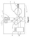
- FIG. 1is a schematic diagram of a wavelength locking apparatus constituting a first embodiment of the present invention.
- FIG. 2is a schematic diagram of a wavelength locking apparatus constituting a second embodiment of the present invention.
- a laser devicefor example a semiconductor laser diode 100 is disposed in a package 102 and is ultimately arranged (although not shown) to launch light into an optical fibre (not shown) downstream of package 102 .
- a collimating lens 104in this example a ball lens, is disposed adjacent the laser diode 100 in the path of the light from laser diode 100 to produce a collimated beam 110 (sometimes referred to as first optical path 110 ).
- a reflective component 108in this example a bulk component double having a first partially reflective surface 109 substantially opposite a second partially reflective surface 111 , acts as a double beam splitter and is disposed in first optical path 110 adjacent the collimating lens 104 .
- Surfaces 109 and 111are on opposite substantially parallel faces of reflective component 108 .
- a dual photodiode 112is disposed.
- the dual photodiode 112comprises a first photodiode 114 disposed at a predetermined spacing adjacent a second photodiode 116 ; photodiodes 114 and 116 are carried by the same substrate.
- the beam splitter 108is placed and aligned to direct light along a second optical path 118 towards the first photodiode 114 .
- the placement and alignment of the beam splitter 108are such so as to direct light along a third optical path 120 towards the second photodiode 116 adjacent the first photodiode 114 .
- An angle at which the beam splitter 108 is disposed relative to the first optical path 110is one factor that dictates the direction of the second and third optical paths 118 , 120 . Another factor is the relative position of the first partially reflective surface 109 and the second partially reflective surface 111 which can be varied so as to control respective reflection towards the first and second photodiodes 114 , 116 .
- a wavelength discriminator 122for example an edge filter or etalon, is disposed adjacent the second photodiode 116 and in the third optical path 120 .
- light emitted by the laser diode 100follows the first optical path 110 and is collimated by the collimating lens 104 before propagating towards the beam splitter 108 .
- a first portion of the light energy emitted by the laser diode 100is reflected by the first partially reflective surface 109 towards the first photodiode 114 along the second optical path 118 .
- a second portion of the light energy emitted by the laser diode 100is reflected by the second partially reflective surface 111 towards the second photodiode 116 along the third optical path 120 .
- Most of the remaining, unreflected, lightpropagates through the beam splitter 108 so as to continue substantially along the first optical path 110 and exit the package 102 .
- the onward propagation of the remaining, unreflected, lightis not relevant for the purpose of describing examples of the invention and is not described further.
- wavelength discriminator 122Depending upon the wavelength of the light emitted by the laser diode 100 , a fraction of the second portion of the light energy emitted by the laser diode 100 is coupled through the wavelength discriminator 122 towards the second photodiode 116 .
- the use and calibration of wavelength discriminators in wavelength monitoring apparatusis known in the art and so is not described further.
- An output ratio calculator unit(not shown) coupled and responsive to electrical output signals of the first and second photodiodes 114 , 116 , for example as described in U.S. Pat. No. 6,144,025, generates an error signal.
- the error signalcan be used by a driver circuit (not shown) for the laser diode 100 .
- the driver circuitis, for example, a proportional integral differential (PID) controller to influence the wavelength of the light generated by the laser diode 100 to ensure that the wavelength of the light generated by the laser diode 100 remains substantially at a required wavelength.
- the wavelength of light generated by the laser diode 100can be controlled, e.g., by controlling the temperature of the laser diode 100 , or if more than one current is applied to the laser diode 100 , controlling one or more of those currents partially.
- the partially reflective surfaces 109 , 111can be provided with, in part, or substantially completely, one or more reflective coatings.
- One or more parts of the partially reflective surfaces 109 , 111can be provided with an anti-reflection coating to prevent internal back reflections by the second partially reflective surface 111 .
- the beam splitter 108can be formed from any suitable at least partially light-transmissive material, such as suitably finished silicon or silica.
- the apparatus of FIG. 1is modified to include an optical isolator 124 positioned adjacent and downstream the beam splitter 108 to receive light in path 110 propagating through the beam splitter 108 .
- the isolator 124is any suitable known isolator that transmits optical energy in only one direction and prevents the electromagnetic radiation that has propagated through the beam splitter 108 , or any means/device(s) for directing the electromagnetic radiation, from being fed back to the laser device 100 and/or detectors 114 and 116 .
- the above embodimentcan be modified by replacing the apparatus for monitoring wavelength with any suitable component arrangement for measuring the wavelength of optical electromagnetic radiation and where one or more devices are employed for directing optical electromagnetic radiation.
- the device for directing electromagnetic radiationenables a portion of the optical electromagnetic radiation incident on it to propagate through it without substantial reflection and or direction change.
- the optical isolatoris not disposed as is conventionally the case as near to the laser as possible, either adjacent the laser, or adjacent the lens, if there is insufficient space between the laser and the lens, but at the “output” of the means for directing electromagnetic radiation, for example as the “output” of beam splitter 108 .
- any of the apparatus described above constituting a component configuration for monitoring a wavelength of electromagnetic radiationis disposed on a base, for example a bench such as a silicon bench.
- the silicon benchis formed by any suitable known semiconductor processing technique that causes, inter alia, one or more recesses to be formed on the bench for one or more components, respectively.
- a suitable fabrication techniqueis micromachining. Reference features are fabricated, such as a fiducial or a v-groove on the silicon optical bench to enable components to be precisely placed on the silicon bench.
- the one or more componentsare bonded to the silicon bench using a suitable adhesive, such as an epoxy adhesive.
- one or more devicescan be grown on the silicon bench.
Landscapes
- Physics & Mathematics (AREA)
- Condensed Matter Physics & Semiconductors (AREA)
- General Physics & Mathematics (AREA)
- Electromagnetism (AREA)
- Optics & Photonics (AREA)
- Optical Couplings Of Light Guides (AREA)
- Semiconductor Lasers (AREA)
Abstract
Description
where:
- F is the coefficient of finesse,
- n is the refractive index of the etalon,
- d is the thickness of the etalon, and
- λ0is the wavelength of operation.
Claims (6)
Priority Applications (1)
| Application Number | Priority Date | Filing Date | Title |
|---|---|---|---|
| US12/169,867US7710581B2 (en) | 2002-03-16 | 2008-07-09 | Wavelength monitoring method and apparatus and method of making same |
Applications Claiming Priority (5)
| Application Number | Priority Date | Filing Date | Title |
|---|---|---|---|
| EP02251899AEP1345298A1 (en) | 2002-03-16 | 2002-03-16 | Wavelength monitoring apparatus and method therefor |
| EP02251899.7 | 2002-03-16 | ||
| EP02251899 | 2002-03-16 | ||
| US10/388,771US7418025B2 (en) | 2002-03-16 | 2003-03-17 | Wavelength monitoring method and apparatus and method of making same |
| US12/169,867US7710581B2 (en) | 2002-03-16 | 2008-07-09 | Wavelength monitoring method and apparatus and method of making same |
Related Parent Applications (1)
| Application Number | Title | Priority Date | Filing Date |
|---|---|---|---|
| US10/388,771DivisionUS7418025B2 (en) | 2002-03-16 | 2003-03-17 | Wavelength monitoring method and apparatus and method of making same |
Publications (2)
| Publication Number | Publication Date |
|---|---|
| US20080291450A1 US20080291450A1 (en) | 2008-11-27 |
| US7710581B2true US7710581B2 (en) | 2010-05-04 |
Family
ID=27763448
Family Applications (2)
| Application Number | Title | Priority Date | Filing Date |
|---|---|---|---|
| US10/388,771Expired - LifetimeUS7418025B2 (en) | 2002-03-16 | 2003-03-17 | Wavelength monitoring method and apparatus and method of making same |
| US12/169,867Expired - Fee RelatedUS7710581B2 (en) | 2002-03-16 | 2008-07-09 | Wavelength monitoring method and apparatus and method of making same |
Family Applications Before (1)
| Application Number | Title | Priority Date | Filing Date |
|---|---|---|---|
| US10/388,771Expired - LifetimeUS7418025B2 (en) | 2002-03-16 | 2003-03-17 | Wavelength monitoring method and apparatus and method of making same |
Country Status (2)
| Country | Link |
|---|---|
| US (2) | US7418025B2 (en) |
| EP (1) | EP1345298A1 (en) |
Cited By (6)
| Publication number | Priority date | Publication date | Assignee | Title |
|---|---|---|---|---|
| EP2770590A1 (en)* | 2013-02-22 | 2014-08-27 | EMCORE Corporation | Small packaged tunable laser assembly |
| US8923348B2 (en) | 2009-08-06 | 2014-12-30 | Emcore Corporation | Small packaged tunable laser assembly |
| US20150030042A1 (en)* | 2012-01-13 | 2015-01-29 | Phovel.Co.Ltd | Wavelength-tunable laser apparatus having wavelength measuring function |
| US9054480B2 (en) | 2009-08-06 | 2015-06-09 | Neophotonics Corporation | Small packaged tunable traveling wave laser assembly |
| US20150162990A1 (en)* | 2013-12-09 | 2015-06-11 | Emcore Corporation | Small packaged tunable laser transmitter |
| US9337611B2 (en) | 2009-08-06 | 2016-05-10 | Neophotonics Corporation | Small packaged tunable laser transmitter |
Families Citing this family (9)
| Publication number | Priority date | Publication date | Assignee | Title |
|---|---|---|---|---|
| GB2429766A (en)* | 2005-09-06 | 2007-03-07 | Bookham Technology Plc | Light monitoring device |
| DE102008058002A1 (en)* | 2008-11-19 | 2010-05-20 | Osram Opto Semiconductors Gmbh | Wavelength stabilized laser has laser medium, which emits primary radiation, and folded external resonator having three resonator mirrors, one of which is designed as folding mirror |
| TWI442031B (en)* | 2011-06-17 | 2014-06-21 | Chroma Ate Inc | Optical measurement system and the device thereof |
| US11437774B2 (en) | 2015-08-19 | 2022-09-06 | Kyocera Sld Laser, Inc. | High-luminous flux laser-based white light source |
| US10365162B2 (en) | 2016-05-27 | 2019-07-30 | Goodrich Corporation | Laser wavelength detectors |
| US20180375574A1 (en)* | 2017-06-27 | 2018-12-27 | Afl Telecommunications Llc | Optical power measurement apparatus |
| US10771153B2 (en) | 2017-06-27 | 2020-09-08 | Afl Telecommunications Llc | Optical power measurement apparatus |
| CN107560831A (en)* | 2017-08-29 | 2018-01-09 | 京东方科技集团股份有限公司 | A kind of color parameter measurement apparatus and its measuring method |
| US11239637B2 (en)* | 2018-12-21 | 2022-02-01 | Kyocera Sld Laser, Inc. | Fiber delivered laser induced white light system |
Citations (27)
| Publication number | Priority date | Publication date | Assignee | Title |
|---|---|---|---|---|
| US4309671A (en) | 1977-10-26 | 1982-01-05 | The Post Office | Control apparatus |
| US4897711A (en) | 1988-03-03 | 1990-01-30 | American Telephone And Telegraph Company | Subassembly for optoelectronic devices |
| WO1998043327A2 (en) | 1997-03-26 | 1998-10-01 | Siemens Aktiengesellschaft | Method for stabilizing the wavelength of a laser and arrangement for implementing said method |
| US5825792A (en) | 1996-07-11 | 1998-10-20 | Northern Telecom Limited | Wavelength monitoring and control assembly for WDM optical transmission systems |
| US6134253A (en)* | 1998-02-19 | 2000-10-17 | Jds Uniphase Corporation | Method and apparatus for monitoring and control of laser emission wavelength |
| US6144025A (en) | 1999-01-13 | 2000-11-07 | Santec Corporation | Laser light source apparatus |
| US6181412B1 (en) | 1998-06-18 | 2001-01-30 | Agence Spatiale Europeene | Incoherent doppler laser detection and ranging system |
| US20010036206A1 (en) | 1999-09-20 | 2001-11-01 | Jerman John H. | Tunable laser with microactuator |
| US20020012369A1 (en) | 2000-05-16 | 2002-01-31 | Hideyuki Nasu | Semiconductor laser apparatus, semiconductor laser module, optical transmitter and wavelength division multiplexing communication system |
| US6400739B1 (en) | 1998-06-22 | 2002-06-04 | Siemens Aktiengesellschaft | Wavelength-stabilized laser configuration |
| US20020071458A1 (en)* | 2000-12-13 | 2002-06-13 | Takami Iwafuji | Version with markings to show changes made |
| US20020075912A1 (en) | 2000-12-18 | 2002-06-20 | Nec Corporation | Wavelength stabilizing unit and wavelength stabilized laser module |
| US20020096728A1 (en) | 1999-07-30 | 2002-07-25 | Werner Kuhlmann | Photodetector for ultraviolet light radiation |
| US20030016707A1 (en) | 2000-07-27 | 2003-01-23 | Mcdonald Mark | Wavelength reference apparatus and method |
| US20030072336A1 (en) | 2001-09-13 | 2003-04-17 | Spectra-Physics Lasers, Inc. | Miniaturized internal laser stabilizing apparatus with inline output for fiber optic applications |
| US6567437B1 (en)* | 2000-01-31 | 2003-05-20 | Mitsubishi Denki Kabushiki Kaisha | Wavelength monitoring device and its adjusting method, and wavelength stabilizing light source and transmission system having plural wavelength stabilizing light source |
| US6661818B1 (en)* | 2000-04-05 | 2003-12-09 | Digital Optics Corporation | Etalon, a wavelength monitor/locker using the etalon and associated methods |
| US6683295B2 (en)* | 2001-10-01 | 2004-01-27 | Digital Optics Corp. | Reduced noise wavelength locker module |
| US6693932B2 (en)* | 2001-03-14 | 2004-02-17 | Opnext Japan, Inc. | Optical wavelength stabilization circuit, optical transmitter and optical transmission system |
| US6765940B2 (en) | 2001-11-01 | 2004-07-20 | Agility Communications, Inc. | Anamorphic prism wavelength locker |
| US6826211B2 (en) | 2001-06-27 | 2004-11-30 | Hitachi, Ltd. | Diode laser controling module and applied equipment thereof |
| US7038782B2 (en)* | 2001-12-11 | 2006-05-02 | Adc Telecommunications, Inc. | Robust wavelength locker for control of laser wavelength |
| US7061947B2 (en) | 2001-11-01 | 2006-06-13 | Agility Communications, Inc. | Partially mirrored beam tap for wavelength lockers |
| US7085448B2 (en)* | 2003-03-12 | 2006-08-01 | Franco Delpiano | Optical wavelength control system |
| US7092416B2 (en)* | 2000-04-05 | 2006-08-15 | Digital Optics Corporation | Integrated wavelength locker for use with more than one wavelength and associated methods |
| US7133136B2 (en)* | 2003-10-22 | 2006-11-07 | Jds Uniphase Corporation | Wavelength monitor |
| US7146064B2 (en)* | 2001-12-21 | 2006-12-05 | Gsi Group Corporation | System and method for producing optical circuits |
- 2002
- 2002-03-16EPEP02251899Apatent/EP1345298A1/ennot_activeWithdrawn
- 2003
- 2003-03-17USUS10/388,771patent/US7418025B2/ennot_activeExpired - Lifetime
- 2008
- 2008-07-09USUS12/169,867patent/US7710581B2/ennot_activeExpired - Fee Related
Patent Citations (29)
| Publication number | Priority date | Publication date | Assignee | Title |
|---|---|---|---|---|
| US4309671A (en) | 1977-10-26 | 1982-01-05 | The Post Office | Control apparatus |
| US4897711A (en) | 1988-03-03 | 1990-01-30 | American Telephone And Telegraph Company | Subassembly for optoelectronic devices |
| US5825792A (en) | 1996-07-11 | 1998-10-20 | Northern Telecom Limited | Wavelength monitoring and control assembly for WDM optical transmission systems |
| WO1998043327A2 (en) | 1997-03-26 | 1998-10-01 | Siemens Aktiengesellschaft | Method for stabilizing the wavelength of a laser and arrangement for implementing said method |
| US6134253A (en)* | 1998-02-19 | 2000-10-17 | Jds Uniphase Corporation | Method and apparatus for monitoring and control of laser emission wavelength |
| US6181412B1 (en) | 1998-06-18 | 2001-01-30 | Agence Spatiale Europeene | Incoherent doppler laser detection and ranging system |
| US6400739B1 (en) | 1998-06-22 | 2002-06-04 | Siemens Aktiengesellschaft | Wavelength-stabilized laser configuration |
| US6144025A (en) | 1999-01-13 | 2000-11-07 | Santec Corporation | Laser light source apparatus |
| US20020096728A1 (en) | 1999-07-30 | 2002-07-25 | Werner Kuhlmann | Photodetector for ultraviolet light radiation |
| US20010036206A1 (en) | 1999-09-20 | 2001-11-01 | Jerman John H. | Tunable laser with microactuator |
| US6567437B1 (en)* | 2000-01-31 | 2003-05-20 | Mitsubishi Denki Kabushiki Kaisha | Wavelength monitoring device and its adjusting method, and wavelength stabilizing light source and transmission system having plural wavelength stabilizing light source |
| US7092416B2 (en)* | 2000-04-05 | 2006-08-15 | Digital Optics Corporation | Integrated wavelength locker for use with more than one wavelength and associated methods |
| US6661818B1 (en)* | 2000-04-05 | 2003-12-09 | Digital Optics Corporation | Etalon, a wavelength monitor/locker using the etalon and associated methods |
| US7466729B2 (en)* | 2000-04-05 | 2008-12-16 | Tessera North America, Inc. | Wavelength monitor for use with more than one wavelength |
| US20020012369A1 (en) | 2000-05-16 | 2002-01-31 | Hideyuki Nasu | Semiconductor laser apparatus, semiconductor laser module, optical transmitter and wavelength division multiplexing communication system |
| US20030016707A1 (en) | 2000-07-27 | 2003-01-23 | Mcdonald Mark | Wavelength reference apparatus and method |
| US7120176B2 (en)* | 2000-07-27 | 2006-10-10 | Intel Corporation | Wavelength reference apparatus and method |
| US20020071458A1 (en)* | 2000-12-13 | 2002-06-13 | Takami Iwafuji | Version with markings to show changes made |
| US20020075912A1 (en) | 2000-12-18 | 2002-06-20 | Nec Corporation | Wavelength stabilizing unit and wavelength stabilized laser module |
| US6693932B2 (en)* | 2001-03-14 | 2004-02-17 | Opnext Japan, Inc. | Optical wavelength stabilization circuit, optical transmitter and optical transmission system |
| US6826211B2 (en) | 2001-06-27 | 2004-11-30 | Hitachi, Ltd. | Diode laser controling module and applied equipment thereof |
| US20030072336A1 (en) | 2001-09-13 | 2003-04-17 | Spectra-Physics Lasers, Inc. | Miniaturized internal laser stabilizing apparatus with inline output for fiber optic applications |
| US6683295B2 (en)* | 2001-10-01 | 2004-01-27 | Digital Optics Corp. | Reduced noise wavelength locker module |
| US7061947B2 (en) | 2001-11-01 | 2006-06-13 | Agility Communications, Inc. | Partially mirrored beam tap for wavelength lockers |
| US6765940B2 (en) | 2001-11-01 | 2004-07-20 | Agility Communications, Inc. | Anamorphic prism wavelength locker |
| US7038782B2 (en)* | 2001-12-11 | 2006-05-02 | Adc Telecommunications, Inc. | Robust wavelength locker for control of laser wavelength |
| US7146064B2 (en)* | 2001-12-21 | 2006-12-05 | Gsi Group Corporation | System and method for producing optical circuits |
| US7085448B2 (en)* | 2003-03-12 | 2006-08-01 | Franco Delpiano | Optical wavelength control system |
| US7133136B2 (en)* | 2003-10-22 | 2006-11-07 | Jds Uniphase Corporation | Wavelength monitor |
Cited By (8)
| Publication number | Priority date | Publication date | Assignee | Title |
|---|---|---|---|---|
| US8923348B2 (en) | 2009-08-06 | 2014-12-30 | Emcore Corporation | Small packaged tunable laser assembly |
| US9054480B2 (en) | 2009-08-06 | 2015-06-09 | Neophotonics Corporation | Small packaged tunable traveling wave laser assembly |
| US9337611B2 (en) | 2009-08-06 | 2016-05-10 | Neophotonics Corporation | Small packaged tunable laser transmitter |
| US20150030042A1 (en)* | 2012-01-13 | 2015-01-29 | Phovel.Co.Ltd | Wavelength-tunable laser apparatus having wavelength measuring function |
| US9325154B2 (en)* | 2012-01-13 | 2016-04-26 | Phovel. Co. Ltd | Wavelength-tunable laser apparatus having wavelength measuring function |
| EP2770590A1 (en)* | 2013-02-22 | 2014-08-27 | EMCORE Corporation | Small packaged tunable laser assembly |
| US20150162990A1 (en)* | 2013-12-09 | 2015-06-11 | Emcore Corporation | Small packaged tunable laser transmitter |
| US9246595B2 (en)* | 2013-12-09 | 2016-01-26 | Neophotonics Corporation | Small packaged tunable laser transmitter |
Also Published As
| Publication number | Publication date |
|---|---|
| EP1345298A1 (en) | 2003-09-17 |
| US20080291450A1 (en) | 2008-11-27 |
| US20030214985A1 (en) | 2003-11-20 |
| US7418025B2 (en) | 2008-08-26 |
Similar Documents
| Publication | Publication Date | Title |
|---|---|---|
| US7710581B2 (en) | Wavelength monitoring method and apparatus and method of making same | |
| US6700664B1 (en) | Optical channel monitoring device | |
| US6621580B2 (en) | Single etalon wavelength locker | |
| US6323987B1 (en) | Controlled multi-wavelength etalon | |
| EP0875743B1 (en) | A wavemeter and an arrangement for the adjustment of the wavelength of an optical source | |
| US6661818B1 (en) | Etalon, a wavelength monitor/locker using the etalon and associated methods | |
| US6859284B2 (en) | Apparatus and method for determining wavelength from coarse and fine measurements | |
| US7466729B2 (en) | Wavelength monitor for use with more than one wavelength | |
| US20170302051A1 (en) | Wavelength locker using multiple feedback curves to wavelength lock a beam | |
| US12072240B2 (en) | Wavelength reference device | |
| US6992774B2 (en) | Wavelength determining apparatus and method | |
| CN111742190B (en) | Beam guiding in an interferometer | |
| EP1158630B1 (en) | Wavelength stabilization monitor and method for adjusting the working wavelength of said monitor | |
| JP2003124566A (en) | Semiconductor laser control module and optical system | |
| US20050088658A1 (en) | Wavelength monitor | |
| US20030099265A1 (en) | Optical apparatus and method therefor | |
| US20030227949A1 (en) | Integrated, temperature insensitive wavelength locker for use in laser packages | |
| CN112236958B (en) | Optical filter control | |
| KR20010073962A (en) | Monitoring method and light source module for wavelength locking | |
| JP2025524589A (en) | Laser frequency stabilization device, frequency stabilization method, and frequency measurement method | |
| US20240280756A1 (en) | Optical assembly with an optical element to suppress a parasitic etalon response | |
| EP1381090A1 (en) | Wavelength detector apparatus and method therefor | |
| EP1320156A1 (en) | Control loop apparatus and method therefor | |
| JP2004526975A (en) | system | |
| JPH02122292A (en) | distance measuring device |
Legal Events
| Date | Code | Title | Description |
|---|---|---|---|
| STCF | Information on status: patent grant | Free format text:PATENTED CASE | |
| FPAY | Fee payment | Year of fee payment:4 | |
| AS | Assignment | Owner name:DEUTSCHE BANK AG NEW YORK BRANCH, AS COLLATERAL AGENT, NEW YORK Free format text:PATENT SECURITY AGREEMENT;ASSIGNOR:AVAGO TECHNOLOGIES GENERAL IP (SINGAPORE) PTE. LTD.;REEL/FRAME:032851/0001 Effective date:20140506 Owner name:DEUTSCHE BANK AG NEW YORK BRANCH, AS COLLATERAL AG Free format text:PATENT SECURITY AGREEMENT;ASSIGNOR:AVAGO TECHNOLOGIES GENERAL IP (SINGAPORE) PTE. LTD.;REEL/FRAME:032851/0001 Effective date:20140506 | |
| AS | Assignment | Owner name:AVAGO TECHNOLOGIES GENERAL IP (SINGAPORE) PTE. LTD., SINGAPORE Free format text:TERMINATION AND RELEASE OF SECURITY INTEREST IN PATENT RIGHTS (RELEASES RF 032851-0001);ASSIGNOR:DEUTSCHE BANK AG NEW YORK BRANCH, AS COLLATERAL AGENT;REEL/FRAME:037689/0001 Effective date:20160201 Owner name:AVAGO TECHNOLOGIES GENERAL IP (SINGAPORE) PTE. LTD Free format text:TERMINATION AND RELEASE OF SECURITY INTEREST IN PATENT RIGHTS (RELEASES RF 032851-0001);ASSIGNOR:DEUTSCHE BANK AG NEW YORK BRANCH, AS COLLATERAL AGENT;REEL/FRAME:037689/0001 Effective date:20160201 | |
| AS | Assignment | Owner name:BANK OF AMERICA, N.A., AS COLLATERAL AGENT, NORTH CAROLINA Free format text:PATENT SECURITY AGREEMENT;ASSIGNOR:AVAGO TECHNOLOGIES GENERAL IP (SINGAPORE) PTE. LTD.;REEL/FRAME:037808/0001 Effective date:20160201 Owner name:BANK OF AMERICA, N.A., AS COLLATERAL AGENT, NORTH Free format text:PATENT SECURITY AGREEMENT;ASSIGNOR:AVAGO TECHNOLOGIES GENERAL IP (SINGAPORE) PTE. LTD.;REEL/FRAME:037808/0001 Effective date:20160201 | |
| AS | Assignment | Owner name:AVAGO TECHNOLOGIES GENERAL IP (SINGAPORE) PTE. LTD., SINGAPORE Free format text:TERMINATION AND RELEASE OF SECURITY INTEREST IN PATENTS;ASSIGNOR:BANK OF AMERICA, N.A., AS COLLATERAL AGENT;REEL/FRAME:041710/0001 Effective date:20170119 Owner name:AVAGO TECHNOLOGIES GENERAL IP (SINGAPORE) PTE. LTD Free format text:TERMINATION AND RELEASE OF SECURITY INTEREST IN PATENTS;ASSIGNOR:BANK OF AMERICA, N.A., AS COLLATERAL AGENT;REEL/FRAME:041710/0001 Effective date:20170119 | |
| MAFP | Maintenance fee payment | Free format text:PAYMENT OF MAINTENANCE FEE, 8TH YEAR, LARGE ENTITY (ORIGINAL EVENT CODE: M1552) Year of fee payment:8 | |
| AS | Assignment | Owner name:AVAGO TECHNOLOGIES INTERNATIONAL SALES PTE. LIMITE Free format text:MERGER;ASSIGNOR:AVAGO TECHNOLOGIES GENERAL IP (SINGAPORE) PTE. LTD.;REEL/FRAME:047196/0687 Effective date:20180509 | |
| AS | Assignment | Owner name:AVAGO TECHNOLOGIES INTERNATIONAL SALES PTE. LIMITE Free format text:CORRECTIVE ASSIGNMENT TO CORRECT THE EFFECTIVE DATE OF MERGER TO 9/5/2018 PREVIOUSLY RECORDED AT REEL: 047196 FRAME: 0687. ASSIGNOR(S) HEREBY CONFIRMS THE MERGER;ASSIGNOR:AVAGO TECHNOLOGIES GENERAL IP (SINGAPORE) PTE. LTD.;REEL/FRAME:047630/0344 Effective date:20180905 | |
| AS | Assignment | Owner name:AVAGO TECHNOLOGIES INTERNATIONAL SALES PTE. LIMITE Free format text:CORRECTIVE ASSIGNMENT TO CORRECT THE PROPERTY NUMBERS PREVIOUSLY RECORDED AT REEL: 47630 FRAME: 344. ASSIGNOR(S) HEREBY CONFIRMS THE ASSIGNMENT;ASSIGNOR:AVAGO TECHNOLOGIES GENERAL IP (SINGAPORE) PTE. LTD.;REEL/FRAME:048883/0267 Effective date:20180905 | |
| AS | Assignment | Owner name:BROADCOM INTERNATIONAL PTE. LTD., SINGAPORE Free format text:ASSIGNMENT OF ASSIGNORS INTEREST;ASSIGNOR:AVAGO TECHNOLOGIES INTERNATIONAL SALES PTE. LIMITED;REEL/FRAME:053771/0901 Effective date:20200826 | |
| LAPS | Lapse for failure to pay maintenance fees | Free format text:PATENT EXPIRED FOR FAILURE TO PAY MAINTENANCE FEES (ORIGINAL EVENT CODE: EXP.); ENTITY STATUS OF PATENT OWNER: LARGE ENTITY | |
| FEPP | Fee payment procedure | Free format text:MAINTENANCE FEE REMINDER MAILED (ORIGINAL EVENT CODE: REM.); ENTITY STATUS OF PATENT OWNER: LARGE ENTITY | |
| STCH | Information on status: patent discontinuation | Free format text:PATENT EXPIRED DUE TO NONPAYMENT OF MAINTENANCE FEES UNDER 37 CFR 1.362 | |
| FP | Lapsed due to failure to pay maintenance fee | Effective date:20220504 |