US7709968B2 - Micro pin grid array with pin motion isolation - Google Patents
Micro pin grid array with pin motion isolationDownload PDFInfo
- Publication number
- US7709968B2 US7709968B2US10/985,119US98511904AUS7709968B2US 7709968 B2US7709968 B2US 7709968B2US 98511904 AUS98511904 AUS 98511904AUS 7709968 B2US7709968 B2US 7709968B2
- Authority
- US
- United States
- Prior art keywords
- package
- microelectronic
- conductive
- terminals
- flexible substrate
- Prior art date
- Legal status (The legal status is an assumption and is not a legal conclusion. Google has not performed a legal analysis and makes no representation as to the accuracy of the status listed.)
- Expired - Fee Related, expires
Links
Images


Classifications
- H—ELECTRICITY
- H01—ELECTRIC ELEMENTS
- H01L—SEMICONDUCTOR DEVICES NOT COVERED BY CLASS H10
- H01L23/00—Details of semiconductor or other solid state devices
- H01L23/48—Arrangements for conducting electric current to or from the solid state body in operation, e.g. leads, terminal arrangements ; Selection of materials therefor
- H01L23/488—Arrangements for conducting electric current to or from the solid state body in operation, e.g. leads, terminal arrangements ; Selection of materials therefor consisting of soldered or bonded constructions
- H01L23/498—Leads, i.e. metallisations or lead-frames on insulating substrates, e.g. chip carriers
- H01L23/4985—Flexible insulating substrates
- H—ELECTRICITY
- H01—ELECTRIC ELEMENTS
- H01L—SEMICONDUCTOR DEVICES NOT COVERED BY CLASS H10
- H01L23/00—Details of semiconductor or other solid state devices
- H01L23/48—Arrangements for conducting electric current to or from the solid state body in operation, e.g. leads, terminal arrangements ; Selection of materials therefor
- H01L23/488—Arrangements for conducting electric current to or from the solid state body in operation, e.g. leads, terminal arrangements ; Selection of materials therefor consisting of soldered or bonded constructions
- H01L23/498—Leads, i.e. metallisations or lead-frames on insulating substrates, e.g. chip carriers
- H01L23/49811—Additional leads joined to the metallisation on the insulating substrate, e.g. pins, bumps, wires, flat leads
- H—ELECTRICITY
- H01—ELECTRIC ELEMENTS
- H01L—SEMICONDUCTOR DEVICES NOT COVERED BY CLASS H10
- H01L23/00—Details of semiconductor or other solid state devices
- H01L23/48—Arrangements for conducting electric current to or from the solid state body in operation, e.g. leads, terminal arrangements ; Selection of materials therefor
- H01L23/488—Arrangements for conducting electric current to or from the solid state body in operation, e.g. leads, terminal arrangements ; Selection of materials therefor consisting of soldered or bonded constructions
- H01L23/498—Leads, i.e. metallisations or lead-frames on insulating substrates, e.g. chip carriers
- H01L23/49838—Geometry or layout
- H—ELECTRICITY
- H05—ELECTRIC TECHNIQUES NOT OTHERWISE PROVIDED FOR
- H05K—PRINTED CIRCUITS; CASINGS OR CONSTRUCTIONAL DETAILS OF ELECTRIC APPARATUS; MANUFACTURE OF ASSEMBLAGES OF ELECTRICAL COMPONENTS
- H05K3/00—Apparatus or processes for manufacturing printed circuits
- H05K3/30—Assembling printed circuits with electric components, e.g. with resistor
- H05K3/32—Assembling printed circuits with electric components, e.g. with resistor electrically connecting electric components or wires to printed circuits
- H05K3/325—Assembling printed circuits with electric components, e.g. with resistor electrically connecting electric components or wires to printed circuits by abutting or pinching, i.e. without alloying process; mechanical auxiliary parts therefor
- H05K3/326—Assembling printed circuits with electric components, e.g. with resistor electrically connecting electric components or wires to printed circuits by abutting or pinching, i.e. without alloying process; mechanical auxiliary parts therefor the printed circuit having integral resilient or deformable parts, e.g. tabs or parts of flexible circuits
- H—ELECTRICITY
- H01—ELECTRIC ELEMENTS
- H01L—SEMICONDUCTOR DEVICES NOT COVERED BY CLASS H10
- H01L2924/00—Indexing scheme for arrangements or methods for connecting or disconnecting semiconductor or solid-state bodies as covered by H01L24/00
- H01L2924/0001—Technical content checked by a classifier
- H01L2924/0002—Not covered by any one of groups H01L24/00, H01L24/00 and H01L2224/00
- H—ELECTRICITY
- H05—ELECTRIC TECHNIQUES NOT OTHERWISE PROVIDED FOR
- H05K—PRINTED CIRCUITS; CASINGS OR CONSTRUCTIONAL DETAILS OF ELECTRIC APPARATUS; MANUFACTURE OF ASSEMBLAGES OF ELECTRICAL COMPONENTS
- H05K1/00—Printed circuits
- H05K1/02—Details
- H05K1/11—Printed elements for providing electric connections to or between printed circuits
- H05K1/118—Printed elements for providing electric connections to or between printed circuits specially for flexible printed circuits, e.g. using folded portions
- H—ELECTRICITY
- H05—ELECTRIC TECHNIQUES NOT OTHERWISE PROVIDED FOR
- H05K—PRINTED CIRCUITS; CASINGS OR CONSTRUCTIONAL DETAILS OF ELECTRIC APPARATUS; MANUFACTURE OF ASSEMBLAGES OF ELECTRICAL COMPONENTS
- H05K2201/00—Indexing scheme relating to printed circuits covered by H05K1/00
- H05K2201/01—Dielectrics
- H05K2201/0104—Properties and characteristics in general
- H05K2201/0133—Elastomeric or compliant polymer
- H—ELECTRICITY
- H05—ELECTRIC TECHNIQUES NOT OTHERWISE PROVIDED FOR
- H05K—PRINTED CIRCUITS; CASINGS OR CONSTRUCTIONAL DETAILS OF ELECTRIC APPARATUS; MANUFACTURE OF ASSEMBLAGES OF ELECTRICAL COMPONENTS
- H05K2201/00—Indexing scheme relating to printed circuits covered by H05K1/00
- H05K2201/03—Conductive materials
- H05K2201/0332—Structure of the conductor
- H05K2201/0364—Conductor shape
- H05K2201/0367—Metallic bump or raised conductor not used as solder bump
- H—ELECTRICITY
- H05—ELECTRIC TECHNIQUES NOT OTHERWISE PROVIDED FOR
- H05K—PRINTED CIRCUITS; CASINGS OR CONSTRUCTIONAL DETAILS OF ELECTRIC APPARATUS; MANUFACTURE OF ASSEMBLAGES OF ELECTRICAL COMPONENTS
- H05K2201/00—Indexing scheme relating to printed circuits covered by H05K1/00
- H05K2201/09—Shape and layout
- H05K2201/09009—Substrate related
- H05K2201/09063—Holes or slots in insulating substrate not used for electrical connections
- H—ELECTRICITY
- H05—ELECTRIC TECHNIQUES NOT OTHERWISE PROVIDED FOR
- H05K—PRINTED CIRCUITS; CASINGS OR CONSTRUCTIONAL DETAILS OF ELECTRIC APPARATUS; MANUFACTURE OF ASSEMBLAGES OF ELECTRICAL COMPONENTS
- H05K2201/00—Indexing scheme relating to printed circuits covered by H05K1/00
- H05K2201/09—Shape and layout
- H05K2201/09009—Substrate related
- H05K2201/09081—Tongue or tail integrated in planar structure, e.g. obtained by cutting from the planar structure
- H—ELECTRICITY
- H05—ELECTRIC TECHNIQUES NOT OTHERWISE PROVIDED FOR
- H05K—PRINTED CIRCUITS; CASINGS OR CONSTRUCTIONAL DETAILS OF ELECTRIC APPARATUS; MANUFACTURE OF ASSEMBLAGES OF ELECTRICAL COMPONENTS
- H05K2201/00—Indexing scheme relating to printed circuits covered by H05K1/00
- H05K2201/10—Details of components or other objects attached to or integrated in a printed circuit board
- H05K2201/10613—Details of electrical connections of non-printed components, e.g. special leads
- H05K2201/10621—Components characterised by their electrical contacts
- H05K2201/10674—Flip chip
- H—ELECTRICITY
- H05—ELECTRIC TECHNIQUES NOT OTHERWISE PROVIDED FOR
- H05K—PRINTED CIRCUITS; CASINGS OR CONSTRUCTIONAL DETAILS OF ELECTRIC APPARATUS; MANUFACTURE OF ASSEMBLAGES OF ELECTRICAL COMPONENTS
- H05K3/00—Apparatus or processes for manufacturing printed circuits
- H05K3/30—Assembling printed circuits with electric components, e.g. with resistor
- H05K3/32—Assembling printed circuits with electric components, e.g. with resistor electrically connecting electric components or wires to printed circuits
- H05K3/34—Assembling printed circuits with electric components, e.g. with resistor electrically connecting electric components or wires to printed circuits by soldering
- H05K3/341—Surface mounted components
- H05K3/3431—Leadless components
- H05K3/3436—Leadless components having an array of bottom contacts, e.g. pad grid array or ball grid array components
Definitions
- the present inventiongenerally relates to microelectronic packages and more specifically to methods of making and testing microelectronic packages.
- Microelectronic devicessuch as semiconductor chips typically require many input and output connections to other electronic components.
- the input and output contacts of a semiconductor chip or other comparable deviceare generally disposed in grid-like patterns that substantially cover a surface of the device (commonly referred to as an “area array”) or in elongated rows which may extend parallel to and adjacent each edge of the device's front surface, or in the center of the front surface.
- areas arraycommonly referred to as an “area array”
- devices such as chipsmust be physically mounted on a substrate such as a printed circuit board, and the contacts of the device must be electrically connected to electrically conductive features of the circuit board.
- Semiconductor chipsare commonly provided in packages which facilitate handling of the chip during manufacture and during mounting of the chip on an external substrate such as a circuit board or other circuit panel.
- semiconductor chipsare provided in packages suitable for surface mounting.
- Numerous packages of this general typehave been proposed for various applications.
- Most commonly, such packagesinclude a dielectric element, commonly referred to as a “chip carrier” with terminals formed as plated or etched metallic structures on the dielectric. These terminals typically are connected to the contacts of the chip itself by features such as thin traces extending along the chip carrier itself and by fine leads or wires extending between the contacts of the chip and the terminals or traces.
- the packageIn a surface mounting operation, the package is placed onto a circuit board so that each terminal on the package is aligned with a corresponding contact pad on the circuit board. Solder or other bonding material is provided between the terminals and the contact pads.
- the packagecan be permanently bonded in place by heating the assembly so as to melt or “reflow” the solder or otherwise activate the bonding material.
- solder massesin the form of solder balls, typically about 0.1 mm and about 0.8 mm (5 and 30 mils) in diameter, attached to the terminals of the package.
- a package having an array of solder balls projecting from its bottom surfaceis commonly referred to as a ball grid array or “BGA” package.
- Other packages, referred to as land grid array or “LGA” packagesare secured to the substrate by thin layers or lands formed from solder.
- Packages of this typecan be quite compact.
- Certain packages, commonly referred to as “chip scale packages,”occupy an area of the circuit board equal to, or only slightly larger than, the area of the device incorporated in the package. This is advantageous in that it reduces the overall size of the assembly and permits the use of short interconnections between various devices on the substrate, which in turn limits signal propagation time between devices and thus facilitates operation of the assembly at high speeds.
- Assemblies including packagescan suffer from stresses imposed by differential thermal expansion and contraction of the device and the substrate.
- a semiconductor chiptends to expand and contract by an amount different from the amount of expansion and contraction of a circuit board.
- these effectstend to cause the terminals to move relative to the contact pads on the circuit board. This can impose stresses in the solder that connects the terminals to the contact pads on the circuit board.
- semiconductor chip packagescan have terminals that are movable with respect to the chip or other device incorporated in the package. Such movement can compensate to an appreciable degree for differential expansion and contraction.
- test fixtureshaving features arranged to compensate for non-planarity.
- featuresadd to the cost of the test fixture and, in some cases, introduce some unreliability into the test fixture itself. This is particularly undesirable because the test fixture, and the engagement of the device with the test fixture, should be more reliable than the packaged devices themselves in order to provide a meaningful test.
- devices intended for high-frequency operationtypically must be tested by applying high frequency signals. This requirement imposes constraints on the electrical characteristics of the signal paths in the test fixture, which further complicates construction of the test fixture.
- soldertends to accumulate on those parts of the test fixture which engage the solder balls. This accumulation of solder residue can shorten the life of the test fixture and impair its reliability.
- U.S. Pat. No. 4,975,079 issued to Beaman et al.discloses a test socket for chips in which dome-shaped contacts on the test substrate are disposed within conical guides. The chip is forced against the substrate so that the solder balls enter the conical guides and engage the dome-shaped pins on the substrate. Sufficient force is applied so that the dome-shaped pins actually deform the solder balls of the chip.
- a further example of a BGA socketmay be found in commonly assigned U.S. Pat. No. 5,802,699, issued Sep. 8, 1998, the disclosure of which is hereby incorporated by reference herein.
- the '699 patentdiscloses a sheet-like connector having a plurality of holes. Each hole is provided with at least one resilient laminar contact extending inwardly over a hole.
- the bump leads of a BGA deviceare advanced into the holes so that the bump leads are engaged with the contacts.
- the assemblycan be tested, and if found acceptable, the bump leads can be permanently bonded to the contacts.
- a dielectric substratehas a plurality of posts extending upwardly from a front surface.
- the postsmay be arranged in an array of post groups, with each post group defining a gap therebetween.
- a generally laminar contactextends from the top of each post.
- the bump leads of the deviceare each inserted within a respective gap thereby engaging the contacts which wipe against the bump lead as it continues to be inserted.
- distal portions of the contactsdeflect downwardly toward the substrate and outwardly away from the center of the gap as the bump lead is inserted into a gap.
- a method of fabricating an interconnection component for a microelectronic deviceincludes providing a flexible chip carrier having first and second surfaces and coupling a conductive sheet to the first surface of the chip carrier. The conductive sheet is then selectively etched to produce a plurality of substantially rigid posts.
- a compliant layeris provided on the second surface of the support structure and a microelectronic device such as a semiconductor chip is engaged with the compliant layer so that the compliant layer lies between the microelectronic device and the chip carrier, and leaving the posts projecting from the exposed surface of the chip carrier.
- the postsare electrically connected to the microelectronic device.
- the postsform projecting package terminals which can be engaged in a socket or solder-bonded to features of a substrate as, for example, a circuit panel. Because the posts are movable with respect to the microelectronic device, such a package substantially accommodates thermal coefficient of expansion mismatches between the device and a supporting substrate when the device is in use. Moreover, the tips of the posts can be coplanar or nearly coplanar.
- a microelectronic packageincludes a microelectronic element, such as a semiconductor chip, having faces and contacts, and a flexible substrate overlying and spaced from a first face of the microelectronic element.
- the flexible substratemay include a dielectric sheet or a polymeric film.
- the packagealso preferably includes a plurality of conductive terminals exposed at a surface of the flexible substrate, the conductive terminals being electrically interconnected with the microelectronic element.
- the flexible substratemost desirably includes a gap extending at least partially around at least one of the conductive terminals and defining a region holding one or more terminals which region can be displaced at least partially independently of the remainder of the substrate.
- the gapfacilitates flexing of the substrate, and thus facilitates movement of the terminals. This action is useful during engagement of the terminals with a test fixture.
- the flexible substratemay include a plurality of gaps defining a plurality of regions of the substrate.
- each of the conductive terminalsmay be connected with one of the plurality of regions so that the conductive terminals are free to move independently of one another.
- the gap in the flexible substratemay extend more than halfway around the at least one of the conductive terminals to define a flap portion of the flexible substrate that is hingedly connected with a remaining portion of the flexible substrate.
- the conductive terminalsmay be mounted on the flap portion of the flexible substrate.
- the conductive terminalsdesirably face away from the first face of the microelectronic element.
- the conductive terminalsmay include conductive posts that extend from the flexible substrate and project away from the first face of the microelectronic element.
- the tips of the postscan move in horizontal directions upon flexure of the substrate. As further discussed below, this can cause the tips of the posts to wipe across the surfaces of terminals on a test circuit board.
- the microelectronic packagemay also include a support layer disposed between the first face of the microelectronic element and the flexible substrate.
- the support layermay include one or more openings, the openings being partially aligned with the conductive terminals so as to provide asymmetrical support to the terminals. As further explained below, such asymmetrical support can promote tilting of the terminals and wiping action.
- the at least one opening in the support layeris substantially aligned with one of said conductive terminals.
- the support layeroptionally may be formed from a compliant material.
- the gapdefines first and second regions of the flexible substrate, whereby the first region is movable relative to the second region, and the at least one of the conductive terminals lies in the first region of the flexible substrate.
- the gapmay extend at least partially around two or more of the conductive terminals.
- the gapmay also lie between two or more of the conductive terminals.
- the gapmay have an asymmetrical shape, a symmetrical shape, or may be in the form of a circular segment.
- the gapmay also be continuous or intermittent.
- the flexible substratemay have a plurality of gaps that give the substrate a web-like appearance. In this case, the electrically conductive components of the package are provided on the substrate, between the gaps.
- the contacts of the microelectronic elementare desirably accessible at the first face of the microelectronic element. That is, the flexible substrate overlies the front or contact-bearing face of the microelectronic element. However, the microelectronic element may have a second face opposite the first face and the contacts may be accessible at the second face of the microelectronic element.
- the microelectronic packagemay also include conductive elements, such as conductive traces provided on said flexible substrate, for electrically interconnecting said conductive terminals and said microelectronic element.
- conductive elementssuch as conductive traces provided on said flexible substrate, for electrically interconnecting said conductive terminals and said microelectronic element.
- a microelectronic packagein a further aspect of the present invention, includes a microelectronic element having faces and contacts, a support layer, such as a compliant support layer, overlying a first face of the microelectronic element, and a flexible substrate overlying the support layer and spaced from the first face of the microelectronic element.
- the packagealso desirably includes a plurality of conductive terminals exposed at a surface of the flexible substrate, the conductive terminals being electrically interconnected with the microelectronic element.
- the support layerhas at least one opening at least partially aligned with at least one of the conductive terminals. The openings in the support layer enhance flexibility of the substrate in the vicinity of the terminals.
- the terminalsare substantially aligned with the openings of the support layer.
- the conductive terminalsare only partially aligned with the plurality of openings. Stated another way, the terminals are offset with respect to the openings to provide asymmetrical support. As further explained below, this causes the terminals to tilt as the substrate flexes over the openings.
- the conductive terminalsmay include conductive posts extending from the flexible substrate and projecting away from the first face of the microelectronic element.
- a microelectronic packagein still another preferred embodiment, includes a microelectronic element having faces and contacts, a support layer, such as a compliant support layer, overlying a first face of the microelectronic element, the support layer having a plurality of openings, and a plurality of conductive terminals overlying the microelectronic element and being electrically interconnected with the microelectronic element.
- Each conductive terminaldesirably has a base having a first section overlying the support layer and a second section overlying one of the openings of the support layer.
- the terminalsmay be in the form of posts. In this arrangement, the terminals may be physically held over the openings by structures other than a flexible dielectric substrate.
- the traces which connect the terminals to the microelectronic elementmay also serve as flexible mountings for the terminals.
- the support layercan be configured to provide asymmetrical support and to cause the terminals to tilt upon engagement with contact elements as, for example, the contact elements of a test fixture.
- Still further aspects of the present inventionprovide methods of processing microelectronic element.
- a microelectronic packagehaving a microelectronic element, a mounting structure and a plurality of terminals carried on the mounting structure and electrically connected to the microelectronic element, is advanced toward a mating unit such as a test board until the terminals engage contact elements of the mating unit and vertically-directed contact forces applied by the contact elements to the terminals cause the mounting structure to deform so that at least some of the terminals move.
- the deformation of the mounting structuremay cause the terminals to tilt about horizontal axes.
- terminalsare vertically-extensive structures such as posts, this causes the tips of the posts to wipe across the contact elements of the mating unit.
- the mounting structureincludes a flexible substrate having gaps therein, a support layer having openings therein, or both, these features facilitate deformation of the mounting structure.
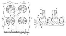
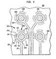
- FIG. 1Ais a fragmentary plan view of a microelectronic package, in accordance with one preferred embodiment of the present invention.
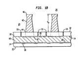
- FIG. 1Bis a cross-sectional view of the package shown in FIG. 1A .
- FIGS. 2A and 2Bshow a fragmentary sectional view of the package of FIG. 1A during a testing operation, in accordance with certain preferred embodiments of the present invention.
- FIG. 3is a diagrammatic elevational view of an assembly including the package of FIGS. 1A-2B .
- FIG. 4shows a fragmentary plan view of a microelectronic package, in accordance with other preferred embodiments of the present invention.
- FIG. 5shows a fragmentary plan view of a microelectronic package, in accordance with another preferred embodiment of the present invention.
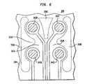
- FIG. 6shows a fragmentary plan view of a microelectronic package, in accordance with yet another preferred embodiment of the present invention.
- FIG. 7shows a fragmentary plan view of a microelectronic package, in accordance with still further preferred embodiments of the present invention.
- FIG. 8Ashows a fragmentary plan view of a microelectronic package, in accordance with yet other preferred embodiments of the present invention.
- FIG. 8Bshows a cross-sectional view of the microelectronic package shown in FIG. 8A .
- FIG. 9Ashows a fragmentary plan view of a microelectronic package, in accordance with still other preferred embodiments of the present invention.
- FIG. 9Bshows a cross-sectional view of the microelectronic package shown in FIG. 9A .
- FIG. 10Ashows a fragmentary plan view of a microelectronic package, in accordance with yet further preferred embodiments of the present invention.
- FIG. 10Bshows a cross-sectional view of the microelectronic package shown in FIG. 10A .
- FIG. 11Ashows a fragmentary plan view of a microelectronic package, in accordance with another preferred embodiment of the present invention.
- FIG. 11Bshows a cross-sectional view of the microelectronic package shown in FIG. 11A .
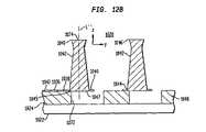
- FIG. 12Ashows a fragmentary plan view of a microelectronic package, in accordance with yet other preferred embodiments of the present invention.
- FIG. 12Bshows a cross-sectional view of the microelectronic package shown in FIG. 12A .
- FIG. 13shows a cross-sectional view of the microelectronic package shown in FIG. 12A during a testing operation.
- FIG. 14shows a cross-sectional view of the microelectronic package, in accordance with still further preferred embodiments of the present invention.
- a microelectronic package 20 in accordance with one embodiment of the present inventionincludes a microelectronic element 22 such as a semiconductor chip having a front or contact-bearing face 24 and electrical contacts 26 exposed at the face 24 .
- a passivation layer 28may be formed over the contact-bearing face 24 with openings at contacts 26 .
- the microelectronic package 20preferably includes a flexible dielectric substrate 30 , such as a polyimide or other polymeric sheet, including a top surface 32 and a bottom surface 34 remote therefrom. Although the thickness of the dielectric substrate 30 may vary depending upon the application, the dielectric substrate most typically is about 15-100 ⁇ m thick.
- the flexible sheet 30has conductive traces 36 thereon. In the particular embodiment illustrated in FIGS. 1A and 1B , the conductive traces are disposed on the bottom surface 34 of the flexible sheet 30 . However, in other embodiments, the conductive traces 36 may extend on the top surface 32 of the flexible sheet 30 ; on both the top and bottom surfaces or within the interior of flexible sheet 30 .
- Conductive traces 36may be formed from any electrically conductive material, but most typically are formed from copper, copper alloys, gold or combinations of these materials. The thickness of the traces 36 may also vary depending upon the application, but typically is about 10-25 ⁇ m. The traces 36 are arranged so that each trace has a post end 38 terminating at a capture pad 40 and a connection end 42 remote from the post end 38 .
- Each post 42is connected to the conductive capture pad 40 at the post end 30 of one of the traces 36 .
- the posts 42extend upwardly through the dielectric sheet 30 from the capture pads 40 of the traces 36 .
- the exact dimensions of the postsmay vary over a significant range but most typically the height H p of each post 42 above the top surface 32 of the flexible sheet 30 is about 50-300 ⁇ m.
- Each post 42has a base 44 adjacent the flexible sheet 30 and a tip 46 remote from the flexible sheet. In the particular embodiment illustrated, the posts extend in directions that are substantially parallel to one another.
- the bases of the poststypically are about 100-600 ⁇ m in diameter, and the tips typically are about 40-200 ⁇ m in diameter.
- the posts 42may be formed from any electrically conductive material, but desirably are formed from metallic material such as copper, copper alloys, gold and combinations thereof.
- the postsmay be formed principally from copper with a layer of gold at the surfaces of the posts.
- the dielectric sheet 30 , traces 36 and posts 42may be fabricated by a process such as that disclosed in co-pending, commonly assigned U.S. provisional patent application Ser. No. 60/508,970, the disclosure of which is incorporated by reference herein.
- a metallic plateis etched or otherwise treated to form numerous metallic posts projecting from the plate.
- a dielectric layeris applied to this plate so that the posts project through the dielectric layer.
- An inner face or side of the dielectric layerfaces toward the metallic plate, whereas the outer side of the dielectric layer faces towards the tips of the posts.
- the dielectric layermay be fabricated by coating a dielectric such as a polyimide onto the plate around the posts or, more typically, by forcibly engaging the posts with the dielectric sheet so that the posts penetrate through the sheet. Once the sheet is in place, the metallic plate is etched to form individual traces on the inner side of the dielectric layer. Alternatively, conventional processes such as plating may form the traces. An etching process may also be used whereby the posts may be formed using the methods disclosed in commonly assigned U.S. Pat. No. 6,177,636, the disclosure of which is hereby incorporated by reference herein. In yet another preferred embodiment, the posts may be fabricated as individual elements and assembled to the flexible sheet in any suitable manner which connects the posts 42 to the traces 36 .
- a dielectricsuch as a polyimide
- the microelectronic package 20also preferably includes a support layer such as a compliant layer 48 disposed between flexible dielectric sheet 30 and front face 24 of semiconductor chip 22 .
- a support layersuch as a compliant layer 48 disposed between flexible dielectric sheet 30 and front face 24 of semiconductor chip 22 .
- the compliant layer 48may be a gel, foam or the like, or a stiffer material such as an epoxy or other adhesive.
- the flexible dielectric substrate 30includes at least one gap 50 formed therein.
- the gap 50may be formed in the flexible substrate 30 by any known method used to perforate a material such as by laser cutting, chemical etching, high pressure liquid stream cutting or mechanical punching.
- a gap 50is formed at least partially around each conductive post 42 .
- the plurality of gaps 50define a plurality of regions 52 of flexible substrate 30 .
- One of the conductive posts 42is mounted on each region 52 defined by one of the gaps 50 .
- Each region 52is connected to the remainder of the substrate 30 by a flap section 54 .
- the conductive traces 36are electrically connected to contacts 43 on the microelectronic element 22 and provide electrically conductive paths between the microelectronic element 22 and the conductive posts 42 .
- contacts 43are disposed in a row along an edge of surface 24 of the microelectronic element 22 .
- the tracesare connected to the contacts by leads 37 formed integrally with traces 36 . Any other suitable connection can be used as, for example, wire bonds extending between the traces and contacts.
- the contacts 43need not be disposed adjacent an edge of the microelectronic element.
- Certain common semiconductor chipshave contacts disposed in arrays distributed over the front surface of the chip, whereas others have contacts disposed in one or more rows near the center of the chip surface.
- the substrate 30 and compliant layer 48may be provided with appropriate apertures, commonly referred to as bond windows, aligned with such contacts.
- a microelectronic package 20is tested by juxtaposing the conductive posts 42 with contact pads 60 on a second microelectronic element 62 such as a circuitized test board ( FIGS. 2A and 2B ).
- the conductive posts 42are placed in substantial alignment with top surfaces 64 of the respective contact pads 60 .
- the top surfacesmay be disposed at different heights so that the top surfaces do not lie in the same plane. Such non-planarity can arise from causes such as warpage of the circuit board 62 itself and unequal thickness of the contact pads 60 .
- the tips 46 of the conductive posts 42may not be precisely co-planar with one another due to such factors as unequal heights of the conductive posts 42 ; non-planarity of the front surface 24 of semiconductor chip 22 and non-uniformity of compliant layer 48 .
- the microelectronic package 20may be tilted slightly with respect to the circuit board 62 . For all of these and other reasons, the vertical distances between the tips 46 of the conductive posts 42 and the top surfaces 64 of the contact pads 60 may be unequal.
- the microelectronic package 20is moved toward the test board 62 by moving the test board, the package or both. Initially, the microelectronic package is moved downward in a direction indicated by axis Z so that the tips 46 of conductive posts 42 engage the top surface 64 of contacts 60 .
- the gap 50 extending through flexible substrate 30enables the region 52 of substrate 30 to have hinge-like movement at flap 54 .
- the base of each conductive post 42is able to move in a generally vertical direction, indicated as direction Z in FIG. 2B , substantially independently of the remainder of the substrate 30 and substantially independently of the other conductive posts.
- Substantially independent movability of the individual posts 42 in the Z directionhelps to assure that all of the posts 42 can be brought into engagement with all of the corresponding contacts 60 simultaneously. This helps to insure reliable electrical interconnections between the tips 46 of conductive posts and contacts 60 .
- each region 52 of the substratetends to bend around the hinge-like flap 54
- each region, and the post 42 connected theretotends to tilt around a theoretical horizontal axis 55 in or near the flap 54 .
- Such tilting movementtends to cause the tip 46 of the post mounted to such flap to move in a horizontal direction indicated by arrow X relative to the remainder of the package, and hence relative to the associated contact 60 , as the tips of the posts engage the contact.
- the postsmove from the starting orientation shown in broken lines in FIG. 2B to the orientation shown in solid lines.
- the horizontal movement of the tips 46causes the tips to wipe across the top surfaces 64 of the contacts, which further aids in establishing reliable electrical connections.
- microelectronic package 20may also be moved in horizontal direction X relative to test board 62 so as to provide additional wiping motion between tip 46 and top surface 64 of contact 60 .
- the microelectronic package 20is tested by applying signals and potentials such as power potentials and ground through the engaged posts 42 and contact pads 60 . After testing, the package is separated from the test board 62 . The package then may be connected to a circuit panel such as a conventional circuit board 70 ( FIG. 3 ) by bonding the posts 42 to the contact pads 72 of the circuit board as, for example, by solder-bonding the tips 46 of the posts to the contact pads.
- the soldermay be applied to the posts or to the contact pads of the circuit board prior to assembly of the package with the circuit board, and reflowed using techniques and equipment commonly used in surface mounting. Most preferably, the solder forms fillets 74 encompassing the tips 46 of the posts.
- the postsreinforce the solder so as to form strong, reliable connections resistant to mechanical fatigue.
- differential thermal expansion and contraction of the microelectronic element 22 and the circuit board 70may tend to move contact pads 72 relative to the microelectronic element.
- the tips 46can move to appreciably accommodate such relative motion and this limit stress on the solder bonds.
- Some of this relative motionmay be provided by flexing of posts 42 .
- the compliant layer 48 and flexible substrate 30continue to allow the bases 44 of the posts to move relative to the microelectronic element.
- the motion of the post basesmay include both linear displacements and tilting as, for example, by bending of the flaps.
- the movement of the post bases 44may include movement of individual regions of the substrate, at least partially independently of movement of other regions of the substrate.
- the gaps which effectively subdivide the substrate into independently movable regionsincrease the movability of the post bases and increase the effective compliance of layer 48 .
- microelectronic package 120in accordance with another preferred embodiment may have features similar to those discussed above with reference to FIGS. 1A-3 .
- microelectronic package 120includes a flexible dielectric substrate 130 having electrically conductive traces 136 , capture pads 140 connected with traces 136 and conductive posts 142 connected with capture pads 140 .
- the flexible dielectric substrate 130has a plurality of gaps 150 extending therethrough.
- a first gap 150 Ais provided around first conductive post 142 A.
- the gap 150 Ais intermittent, and incorporates multiple gap portions 151 interspersed with webs 153 of substrate material.
- Gap 150 Aextends in a circular path at least partially about first conductive post 142 A.
- the first gap 150 Adefines a first region 152 A that is distinct from remaining regions of the flexible dielectric substrate 130 .
- Substrate 130includes second gap 150 B surrounding second conductive post 142 B for defining a second region 152 B of the substrate.
- the substrate 130includes third gap 150 C and fourth gap 150 D.
- the substratehas plural gaps defining a plurality of distinct regions of the flexible substrate.
- one of the conductive postsis located in each such region.
- each conductive postis able to move independently of the other conductive posts.
- the movement of the individual regions relative to the remainder of the substratemay include, for example, flexing of the webs 153 as rather than the flap bending action discussed above.
- FIG. 5shows a microelectronic package 220 in accordance with another embodiment of the present invention.
- adjacent regions 252 A and 252 Bare separated from one another by a common gap 250 A bordering both of these regions.
- the gap 250may be symmetrical or asymmetrical.
- the common gap 250thus at least partially defines a first region 252 A connected with a first conductive post 242 A and a second region 252 B for receiving second conductive post 242 B.
- Regions 252 A and 252 Bare further separated from the remainder of the substrate by additional gaps 250 A and 250 B.
- the individual regions, and hence the individual conductive postsare able to move independently of one another.
- the remaining features of this embodimentmay be similar to those discussed above.
- the flexible substrate 330has a single gap 350 that at least partially surrounds two conductive posts 342 A and 342 B, and at least partially separates a region 352 A carrying both of posts 342 A and 342 B from the remainder of the substrate.
- region 352 Amay flex as a unit, so that the movement of posts 342 A and 342 B are linked to a greater degree than would be the case if each of these posts was disposed on an individual region of the substrate.
- gap 350 Aincludes a section 350 A′ projecting into region 352 A and thus partially subdividing this region into individual regions associated with individual posts.
- the projecting sectionsmay be omitted.
- more than two postsmay be provided on a single region.
- a second gap 350 Bat least partially surrounds third and fourth conductive posts 342 C and 342 D, and at least partially defines a further region 352 B of the substrate.
- Yet another gap 350 Cintervenes between regions 352 A and 352 B.
- the gapsoccupy a substantial portion of the area of the substrate, so that the flexible dielectric substrate has a web-like appearance.
- the flexible dielectric substrateis substantially made up of the regions occupied by the posts and the regions occupied by the traces, with most or all of the other regions omitted.
- Such an arrangementcan be used in embodiments where each post is provided on a separate region. whereby the electrically conductive elements are provided on the substrate and between the gaps.
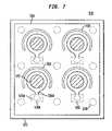
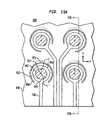
- FIG. 7shows a microelectronic package 520 including a flexible dielectric substrate 530 overlying a semiconductor chip 522 having an area array of contacts 526 .
- the flexible dielectric substrate 530is supported over a contact-bearing face of the semiconductor chip 522 by support elements 570 .
- At least some of the support elements 570are conductive support elements, such as conductive support element 570 A that electrically interconnects contact 526 A with conductive trace 536 A.
- some support elements 570may be used only for supporting flexible dielectric substrate 530 over the contact-bearing face of semiconductor chip 522 while other support elements may be both supportive and conductive for electrically interconnecting one or more conductive posts 542 with the semiconductor chip 522 .
- the support elementsallow the substrate to flex at least in regions of the substrate disposed between the support elements.
- flexure of the support elementallows movement of individual posts. In the embodiment of FIG. 7 , this action is combined with the isolating action of gaps 550 at least partially surrounding and defining individual regions of the substrate, to further promote independent movement of the posts.
- a microelectronic package 620 in accordance with another embodiment of the present inventionincludes a microelectronic element such as a semiconductor chip 622 , a support layer 648 overlying a front face 624 of the semiconductor chip and a flexible dielectric substrate 630 overlying the support layer 648 .
- the support layermay be compliant or rigid.
- the packagefurther includes conductive posts 642 mounted to the flexible dielectric substrate as described above with respect to FIGS. 1A and 1B .
- the conductive posts 642have bases 644 physically connected to the substrate 630 and have tip ends 646 remote from the substrate.
- Each conductive postis attached to a capture pad 640 , which is electrically interconnected with a conductive trace 636 .
- substrate 630does not include gaps as discussed above.
- Support layer 648includes openings 672 . Openings 672 of the support layer are aligned with the respective bases 644 of the conductive posts 642 . Openings 672 in the compliant layer 648 may be formed by etching, punching, laser or high-pressure liquid stream cutting of a continuous layer, or by forming the layer with the openings using a process such as molding or silk-screening of a curable material. Although the openings 672 are depicted as extending entirely through the support layer 648 , this is not essential; the openings should be open to the surface of the support layer confronting the posts and flexible substrate, but need not be open to the opposite surface of the support layer, confronting the microelectronic element 622 .
- each post 642is disposed on a region 652 of the substrate aligned with an opening 672 . Although these regions are not physically separated from the remainder of the substrate, each such region 652 can deform by bowing or bending downwardly into the associated opening 672 . This type of deformation does not require deformation of other portions of the substrate 630 . Where the support layer 648 has appreciable compliance, loads applied to an individual post 642 may also cause some compression of those portions of the support layer surrounding openings 672 .
- the postscan still move independently of one another to a greater degree than would be the case without openings 672 .
- the openingsmaterially increase the effective compliance of the system, as, for example, the motion imparted to a single post 642 by application of a given load to such post.
- FIGS. 9A and 9Bshow a microelectronic package 720 in accordance with another preferred embodiment of the present invention.
- the packageincludes a microelectronic element such as a semiconductor chip 722 , a support layer 748 overlying the chip 722 and a flexible dielectric substrate 730 overlying the support layer 748 .
- the packageincludes conductive posts 742 having bases 744 and tip ends 746 . Each tip end includes a center 774 defining a longitudinal axis L extending the length of the conductive post 742 .
- the base 744 of post 742is connected by with a trace 736 .
- This packageis generally similar to the package described above with reference to FIGS. 8A and 8 B. However, in the package of FIGS.
- the base 744 of each postdoes is not fully aligned with the opening 772 extending through compliant layer 748 .
- the longitudinal axis L of the postis offset in a horizontal direction X from the center C of the associated opening 772 .
- a first or edge region 745 of the conductive post baseoverlies the top surface of support layer 748 and a second or central region 747 of the post base overlies the opening 772 .
- the longitudinal axis L through the tip center 774is aligned with the opening 772 , and thus passes through central region 747 .
- the support layer 748 between the flexible dielectric sheet 730 and the semiconductor chip 722may be substantially rigid.
- Such a support layerprovides particularly good conditions for bonding leads such as a wire bond 776 to one or more of the traces 736 on the flexible substrate.
- the relatively stiff support layerprovides good support for forcible engagement of the wire bond with the trace.
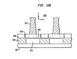
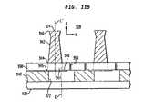
- FIGS. 10A and 10Bshow a microelectronic package 820 that incorporates certain features of the packages described in FIGS. 1A-1B and 8 A- 8 B.
- the microelectronic packageincludes a microelectronic element such as a semiconductor chip 822 , a support layer 848 overlying the front face of the semiconductor chip 822 and a flexible dielectric substrate 830 overlying the support layer 848 .
- the flexible substrate 830has gaps 850 formed therein to provide hinge-like movement for regions 852 of the substrate conductive posts 842 attached thereto.
- the conductive posts 842are aligned with openings 872 extending through support layer 848 .
- the packageprovides Z compliancy as well as axes wiping action for the conductive posts 842 .
- a microelectronic package 920according to yet another embodiment of the present invention ( FIGS. 11A and 11B ) combines certain features described above in the packages shown in FIGS. 1A-1B and 9 A- 9 B.
- the microelectronic package 920includes a microelectronic element such as a semiconductor chip 922 , a support layer 948 overlying the semiconductor chip 922 and a flexible dielectric substrate 930 overlying the support layer 948 .
- the packageincludes conductive traces 936 connected with the bases 944 of conductive posts 942 .
- Each conductive post 942includes a tip 946 having a center 974 defining a longitudinal axis L′ of the conductive post.
- the flexible substrate 930includes gaps 950 formed therein to provide regions 952 of the flexible dielectric substrate 930 that are hingedly connected to the remainder of the dielectric substrate.
- the centers C of openings 972 in the support layerdo not completely coincide with the bases 944 of conductive posts 942 .
- a first section 945 of each conductive post 942overlies the support layer 948 and a second section 947 overlies the opening 972 .
- This arrangementprovides for a hinge-like movement at the base of conductive posts 942 .
- the hinge-like action of the flexible substratecombines with the partial alignment of the conductive post with the opening 972 to provide a tilting action to the post the tip 946 engages a contact pad.
- the microelectronic package 920 of FIGS. 11A and FIG. 11Bcan accommodate for non-planarity as well as provide for wiping motion of the tips 946 of conductive posts 942 .
- FIGS. 12A and 12Bdepict a microelectronic package 1020 including a microelectronic element such as a semiconductor chip 1022 having a contact-bearing face 1024 and a support layer 1048 overlying the contact-bearing face.
- the layer 1048may be a compliant layer or may be substantially non-compliant.
- the microelectronic packageincludes conductive traces 1036 having post ends 1038 terminating at capture pads 1040 and posts 1042 and contact ends 1042 remote from the post ends.
- the packageincludes conductive posts 1042 , each post having a base 1044 and a tip 1046 remote therefrom.
- the traces 1036 and capture pads 1040in conjunction with support layer 1048 , serve as the physical mounting elements which hold the posts 1042 .
- the tip of each posthas a center point 1074 and a longitudinal axis L′′ extends through the center, lengthwise along the post.
- Support layer 1048has openings 1072 extending therethrough. The openings 1072 do not completely coincide with the capture pad 1040 and the base 1044 of conductive post 1042 .
- a first section 1045 of conductive post 1042overlies layer 1048 and a second section 1047 of conductive post 1042 overlies opening 1072 .
- the center point 1074 of tip 1046 and longitudinal axis L′′are aligned with opening 1072 of layer 1048 .
- the post end 1038 of each traceforms a resilient hinge-like connection at the base 1044 of conductive posts 1042 . The hinge-like connection enables the conductive posts to tilt action when the tip ends are abutted against opposing contacts.
- a flexible dielectric substrateis not required; the conductive posts and traces may be disposed directly atop layer 1048 .
- FIG. 13shows the microelectronic package 1020 of FIGS. 12A and 12B during a testing operation.
- the microelectronic package 1020is placed so that the tip ends 1046 of conductive posts 1042 are juxtaposed with top surfaces 1064 of contacts 1060 of a test substrate 1062 .
- the microelectronic package 1020is moved toward the test substrate in a direction indicated by axis Z until the tip ends 1046 engage the top surfaces 1064 of the contact 1060 .
- engagement of the post tips with the contact surfaces 1064causes the posts to tilt as shown in broken lines in FIG. 13 , thus moving the tip of each post independently in the vertical or Z direction, and also providing some wiping motion in the Y direction.
- the microelectronic package as a wholemay be moved relative to test substrate 1062 in the horizontal direction indicated by axis Y to provide additional wiping action.
- FIG. 14shows a microelectronic package 1120 in accordance another embodiment of the present invention.
- the microelectronic package 1120is substantially similar to that shown and described above in FIGS. 1A and 1B .
- the microelectronic package 1120has conductive terminals 1142 in the form of generally planar pads rather than the elongated conductive posts described above.
- a second microelectronic element or test substrate 1162 having conductive probes 1160may be juxtaposed with the conductive terminals 1142 .
- the probesmay be abutted against the top surface 1146 of the conductive terminals 1142 .
- the gaps 1150 provided in flexible dielectric substrate 1130enable each of the conductive terminals 1142 to move independently of one another in a Z direction for forming a more reliable electrical interconnection between the microelectronic package 1120 and the test board 1162 .
- Similar flat pad terminals, and other types of terminalsmay be used in the other arrangements discussed above.
- the support structure which holds the terminalstends to deform in a non-uniform manner so that the terminals tilt.
- the support structurecan include one or more layers of non-uniform compressibility or non-uniform stiffness, so that the vertical compliance of the support structure varies in horizontal directions.
- a particle coatingsuch as that disclosed in U.S. Pat. Nos. 4,804,132 and 5,083,697, the disclosures of which are incorporated by reference herein, may be provided on one or more electrically conductive parts of a microelectronic package for enhancing the formation of electrical interconnections between microelectronic elements and for facilitating testing of microelectronic packages.
- the particle coatingis preferably provided over conductive parts such as conductive terminals or the tip ends of conductive posts.
- the particle coatingis a metalized diamond crystal coating that is selectively electroplated onto the conductive parts of a microelectronic element using standard photoresist techniques.
- a conductive part with the diamond crystal coatingmay be pressed onto an opposing contact pad for piercing the oxidation layer present at the outer surface of the contact pad.
- the diamond crystal coatingfacilitates the formation of reliable electrical interconnections through penetration of oxide layers, in addition to traditional wiping action.
- the postsmay be provided with features which further promote wiping action and otherwise facilitate engagement of the posts and contacts.
- the tip end or upper extremity of each postmay be horizontally offset from the center of the base of that post. Such offset can be used in addition to, or in lieu of, the features discussed above for promoting tilting of the posts.
- the postscan be provided with features such as sharp edges or asperities for promoting more reliable engagement with contact pads.
Landscapes
- Engineering & Computer Science (AREA)
- Microelectronics & Electronic Packaging (AREA)
- Physics & Mathematics (AREA)
- Condensed Matter Physics & Semiconductors (AREA)
- General Physics & Mathematics (AREA)
- Computer Hardware Design (AREA)
- Power Engineering (AREA)
- Metallurgy (AREA)
- Manufacturing & Machinery (AREA)
- Geometry (AREA)
- Testing Of Individual Semiconductor Devices (AREA)
- Lead Frames For Integrated Circuits (AREA)
Abstract
Description
Claims (24)
Priority Applications (3)
| Application Number | Priority Date | Filing Date | Title |
|---|---|---|---|
| US10/985,119US7709968B2 (en) | 2003-12-30 | 2004-11-10 | Micro pin grid array with pin motion isolation |
| PCT/US2004/043049WO2005065238A2 (en) | 2003-12-30 | 2004-12-21 | Micro pin grid array with pin motion isolation |
| US12/759,196US8531039B2 (en) | 2003-12-30 | 2010-04-13 | Micro pin grid array with pin motion isolation |
Applications Claiming Priority (2)
| Application Number | Priority Date | Filing Date | Title |
|---|---|---|---|
| US53343703P | 2003-12-30 | 2003-12-30 | |
| US10/985,119US7709968B2 (en) | 2003-12-30 | 2004-11-10 | Micro pin grid array with pin motion isolation |
Related Child Applications (1)
| Application Number | Title | Priority Date | Filing Date |
|---|---|---|---|
| US12/759,196DivisionUS8531039B2 (en) | 2003-12-30 | 2010-04-13 | Micro pin grid array with pin motion isolation |
Publications (2)
| Publication Number | Publication Date |
|---|---|
| US20050173805A1 US20050173805A1 (en) | 2005-08-11 |
| US7709968B2true US7709968B2 (en) | 2010-05-04 |
Family
ID=34752997
Family Applications (2)
| Application Number | Title | Priority Date | Filing Date |
|---|---|---|---|
| US10/985,119Expired - Fee RelatedUS7709968B2 (en) | 2003-12-30 | 2004-11-10 | Micro pin grid array with pin motion isolation |
| US12/759,196Expired - Fee RelatedUS8531039B2 (en) | 2003-12-30 | 2010-04-13 | Micro pin grid array with pin motion isolation |
Family Applications After (1)
| Application Number | Title | Priority Date | Filing Date |
|---|---|---|---|
| US12/759,196Expired - Fee RelatedUS8531039B2 (en) | 2003-12-30 | 2010-04-13 | Micro pin grid array with pin motion isolation |
Country Status (2)
| Country | Link |
|---|---|
| US (2) | US7709968B2 (en) |
| WO (1) | WO2005065238A2 (en) |
Cited By (38)
| Publication number | Priority date | Publication date | Assignee | Title |
|---|---|---|---|---|
| US20090115047A1 (en)* | 2007-10-10 | 2009-05-07 | Tessera, Inc. | Robust multi-layer wiring elements and assemblies with embedded microelectronic elements |
| US20110304059A1 (en)* | 2010-06-14 | 2011-12-15 | Fujitsu Limited | Circuit board, circuit board assembly, and semiconductor device |
| US8890327B2 (en) | 2005-12-01 | 2014-11-18 | Tessera, Inc. | Stacked microelectronic packages having at least two stacked microelectronic elements adjacent one another |
| US9391008B2 (en) | 2012-07-31 | 2016-07-12 | Invensas Corporation | Reconstituted wafer-level package DRAM |
| US9412714B2 (en) | 2014-05-30 | 2016-08-09 | Invensas Corporation | Wire bond support structure and microelectronic package including wire bonds therefrom |
| US9502390B2 (en) | 2012-08-03 | 2016-11-22 | Invensas Corporation | BVA interposer |
| US9553076B2 (en) | 2010-07-19 | 2017-01-24 | Tessera, Inc. | Stackable molded microelectronic packages with area array unit connectors |
| US9570382B2 (en) | 2010-07-19 | 2017-02-14 | Tessera, Inc. | Stackable molded microelectronic packages |
| US9570416B2 (en) | 2004-11-03 | 2017-02-14 | Tessera, Inc. | Stacked packaging improvements |
| US9583411B2 (en) | 2014-01-17 | 2017-02-28 | Invensas Corporation | Fine pitch BVA using reconstituted wafer with area array accessible for testing |
| US9601454B2 (en) | 2013-02-01 | 2017-03-21 | Invensas Corporation | Method of forming a component having wire bonds and a stiffening layer |
| US9615456B2 (en) | 2012-12-20 | 2017-04-04 | Invensas Corporation | Microelectronic assembly for microelectronic packaging with bond elements to encapsulation surface |
| US9659848B1 (en) | 2015-11-18 | 2017-05-23 | Invensas Corporation | Stiffened wires for offset BVA |
| US9685365B2 (en) | 2013-08-08 | 2017-06-20 | Invensas Corporation | Method of forming a wire bond having a free end |
| US9691679B2 (en) | 2012-02-24 | 2017-06-27 | Invensas Corporation | Method for package-on-package assembly with wire bonds to encapsulation surface |
| US9691731B2 (en) | 2011-05-03 | 2017-06-27 | Tessera, Inc. | Package-on-package assembly with wire bonds to encapsulation surface |
| US9728527B2 (en) | 2013-11-22 | 2017-08-08 | Invensas Corporation | Multiple bond via arrays of different wire heights on a same substrate |
| US9735084B2 (en) | 2014-12-11 | 2017-08-15 | Invensas Corporation | Bond via array for thermal conductivity |
| US9761558B2 (en) | 2011-10-17 | 2017-09-12 | Invensas Corporation | Package-on-package assembly with wire bond vias |
| US9761554B2 (en) | 2015-05-07 | 2017-09-12 | Invensas Corporation | Ball bonding metal wire bond wires to metal pads |
| US9812402B2 (en) | 2015-10-12 | 2017-11-07 | Invensas Corporation | Wire bond wires for interference shielding |
| US9842745B2 (en) | 2012-02-17 | 2017-12-12 | Invensas Corporation | Heat spreading substrate with embedded interconnects |
| US9852969B2 (en) | 2013-11-22 | 2017-12-26 | Invensas Corporation | Die stacks with one or more bond via arrays of wire bond wires and with one or more arrays of bump interconnects |
| US9888579B2 (en) | 2015-03-05 | 2018-02-06 | Invensas Corporation | Pressing of wire bond wire tips to provide bent-over tips |
| US9911718B2 (en) | 2015-11-17 | 2018-03-06 | Invensas Corporation | ‘RDL-First’ packaged microelectronic device for a package-on-package device |
| US9935075B2 (en) | 2016-07-29 | 2018-04-03 | Invensas Corporation | Wire bonding method and apparatus for electromagnetic interference shielding |
| US9984992B2 (en) | 2015-12-30 | 2018-05-29 | Invensas Corporation | Embedded wire bond wires for vertical integration with separate surface mount and wire bond mounting surfaces |
| US9984901B2 (en) | 2005-12-23 | 2018-05-29 | Tessera, Inc. | Method for making a microelectronic assembly having conductive elements |
| US10008469B2 (en) | 2015-04-30 | 2018-06-26 | Invensas Corporation | Wafer-level packaging using wire bond wires in place of a redistribution layer |
| US10008477B2 (en) | 2013-09-16 | 2018-06-26 | Invensas Corporation | Microelectronic element with bond elements to encapsulation surface |
| US10026717B2 (en) | 2013-11-22 | 2018-07-17 | Invensas Corporation | Multiple bond via arrays of different wire heights on a same substrate |
| US10170412B2 (en) | 2012-05-22 | 2019-01-01 | Invensas Corporation | Substrate-less stackable package with wire-bond interconnect |
| US10181457B2 (en) | 2015-10-26 | 2019-01-15 | Invensas Corporation | Microelectronic package for wafer-level chip scale packaging with fan-out |
| US10299368B2 (en) | 2016-12-21 | 2019-05-21 | Invensas Corporation | Surface integrated waveguides and circuit structures therefor |
| US10332854B2 (en) | 2015-10-23 | 2019-06-25 | Invensas Corporation | Anchoring structure of fine pitch bva |
| US10381326B2 (en) | 2014-05-28 | 2019-08-13 | Invensas Corporation | Structure and method for integrated circuits packaging with increased density |
| US10460958B2 (en) | 2013-08-07 | 2019-10-29 | Invensas Corporation | Method of manufacturing embedded packaging with preformed vias |
| US10490528B2 (en) | 2015-10-12 | 2019-11-26 | Invensas Corporation | Embedded wire bond wires |
Families Citing this family (35)
| Publication number | Priority date | Publication date | Assignee | Title |
|---|---|---|---|---|
| US6826827B1 (en)* | 1994-12-29 | 2004-12-07 | Tessera, Inc. | Forming conductive posts by selective removal of conductive material |
| US7183643B2 (en)* | 2003-11-04 | 2007-02-27 | Tessera, Inc. | Stacked packages and systems incorporating the same |
| US20050280134A1 (en)* | 2004-06-18 | 2005-12-22 | Tessera, Inc. | Multi-frequency noise suppression capacitor set |
| US20060027899A1 (en)* | 2004-06-25 | 2006-02-09 | Tessera, Inc. | Structure with spherical contact pins |
| US7453157B2 (en)* | 2004-06-25 | 2008-11-18 | Tessera, Inc. | Microelectronic packages and methods therefor |
| US20060033515A1 (en)* | 2004-08-13 | 2006-02-16 | Tessera, Inc. | Test fixture with movable pin contacts |
| US7687925B2 (en) | 2005-09-07 | 2010-03-30 | Infineon Technologies Ag | Alignment marks for polarized light lithography and method for use thereof |
| JP2007103410A (en)* | 2005-09-30 | 2007-04-19 | Elpida Memory Inc | Semiconductor device with dense contact holes |
| US7453139B2 (en)* | 2005-12-27 | 2008-11-18 | Tessera, Inc. | Compliant terminal mountings with vented spaces and methods |
| US7632708B2 (en)* | 2005-12-27 | 2009-12-15 | Tessera, Inc. | Microelectronic component with photo-imageable substrate |
| US7534652B2 (en)* | 2005-12-27 | 2009-05-19 | Tessera, Inc. | Microelectronic elements with compliant terminal mountings and methods for making the same |
| US7732912B2 (en)* | 2006-08-11 | 2010-06-08 | Tessera, Inc. | Semiconductor chip packages and assemblies with chip carrier units |
| US7545029B2 (en)* | 2006-08-18 | 2009-06-09 | Tessera, Inc. | Stack microelectronic assemblies |
| US8133808B2 (en)* | 2006-09-18 | 2012-03-13 | Tessera, Inc. | Wafer level chip package and a method of fabricating thereof |
| US8258410B2 (en) | 2008-01-26 | 2012-09-04 | International Business Machines Corporation | Construction of reliable stacked via in electronic substrates—vertical stiffness control method |
| US7982316B1 (en)* | 2008-02-04 | 2011-07-19 | Amkor Technology, Inc. | Semiconductor package having a land to absorb thermal and mechanical stress and fabricating method thereof |
| US9006028B2 (en)* | 2008-09-12 | 2015-04-14 | Ananda H. Kumar | Methods for forming ceramic substrates with via studs |
| US8823166B2 (en)* | 2010-08-30 | 2014-09-02 | Taiwan Semiconductor Manufacturing Company, Ltd. | Pillar bumps and process for making same |
| KR101075241B1 (en) | 2010-11-15 | 2011-11-01 | 테세라, 인코포레이티드 | Microelectronic package with terminals in dielectric member |
| US20120146206A1 (en) | 2010-12-13 | 2012-06-14 | Tessera Research Llc | Pin attachment |
| US9137903B2 (en) | 2010-12-21 | 2015-09-15 | Tessera, Inc. | Semiconductor chip assembly and method for making same |
| US8618659B2 (en) | 2011-05-03 | 2013-12-31 | Tessera, Inc. | Package-on-package assembly with wire bonds to encapsulation surface |
| US8872318B2 (en) | 2011-08-24 | 2014-10-28 | Tessera, Inc. | Through interposer wire bond using low CTE interposer with coarse slot apertures |
| US9349706B2 (en) | 2012-02-24 | 2016-05-24 | Invensas Corporation | Method for package-on-package assembly with wire bonds to encapsulation surface |
| US8975738B2 (en) | 2012-11-12 | 2015-03-10 | Invensas Corporation | Structure for microelectronic packaging with terminals on dielectric mass |
| US9023691B2 (en) | 2013-07-15 | 2015-05-05 | Invensas Corporation | Microelectronic assemblies with stack terminals coupled by connectors extending through encapsulation |
| US8883563B1 (en) | 2013-07-15 | 2014-11-11 | Invensas Corporation | Fabrication of microelectronic assemblies having stack terminals coupled by connectors extending through encapsulation |
| US9034696B2 (en) | 2013-07-15 | 2015-05-19 | Invensas Corporation | Microelectronic assemblies having reinforcing collars on connectors extending through encapsulation |
| JP2015060947A (en)* | 2013-09-19 | 2015-03-30 | イビデン株式会社 | Printed wiring board having metal post and method of manufacturing printed wiring board having metal post |
| US9087815B2 (en) | 2013-11-12 | 2015-07-21 | Invensas Corporation | Off substrate kinking of bond wire |
| US9082753B2 (en) | 2013-11-12 | 2015-07-14 | Invensas Corporation | Severing bond wire by kinking and twisting |
| US10090267B2 (en)* | 2014-03-13 | 2018-10-02 | Taiwan Semiconductor Manufacturing Co., Ltd | Bump structure and method for forming the same |
| US9214454B2 (en) | 2014-03-31 | 2015-12-15 | Invensas Corporation | Batch process fabrication of package-on-package microelectronic assemblies |
| US9646917B2 (en) | 2014-05-29 | 2017-05-09 | Invensas Corporation | Low CTE component with wire bond interconnects |
| CN114449751B (en)* | 2021-07-14 | 2023-07-18 | 荣耀终端有限公司 | Circuit board assembly and electronic equipment |
Citations (64)
| Publication number | Priority date | Publication date | Assignee | Title |
|---|---|---|---|---|
| US4695870A (en) | 1986-03-27 | 1987-09-22 | Hughes Aircraft Company | Inverted chip carrier |
| US4716049A (en) | 1985-12-20 | 1987-12-29 | Hughes Aircraft Company | Compressive pedestal for microminiature connections |
| US4804132A (en) | 1987-08-28 | 1989-02-14 | Difrancesco Louis | Method for cold bonding |
| US4902600A (en) | 1986-10-14 | 1990-02-20 | Fuji Photo Film Co., Ltd. | Light-sensitive material comprising light-sensitive layer provided on support wherein the light-sensitive layer and support have specified pH values |
| US4924353A (en) | 1985-12-20 | 1990-05-08 | Hughes Aircraft Company | Connector system for coupling to an integrated circuit chip |
| US4975079A (en)* | 1990-02-23 | 1990-12-04 | International Business Machines Corp. | Connector assembly for chip testing |
| US4982265A (en) | 1987-06-24 | 1991-01-01 | Hitachi, Ltd. | Semiconductor integrated circuit device and method of manufacturing the same |
| US5068714A (en)* | 1989-04-05 | 1991-11-26 | Robert Bosch Gmbh | Method of electrically and mechanically connecting a semiconductor to a substrate using an electrically conductive tacky adhesive and the device so made |
| US5083697A (en) | 1990-02-14 | 1992-01-28 | Difrancesco Louis | Particle-enhanced joining of metal surfaces |
| US5138438A (en) | 1987-06-24 | 1992-08-11 | Akita Electronics Co. Ltd. | Lead connections means for stacked tab packaged IC chips |
| US5148266A (en) | 1990-09-24 | 1992-09-15 | Ist Associates, Inc. | Semiconductor chip assemblies having interposer and flexible lead |
| US5148265A (en)* | 1990-09-24 | 1992-09-15 | Ist Associates, Inc. | Semiconductor chip assemblies with fan-in leads |
| US5189505A (en) | 1989-11-08 | 1993-02-23 | Hewlett-Packard Company | Flexible attachment flip-chip assembly |
| US5196726A (en) | 1990-01-23 | 1993-03-23 | Sumitomo Electric Industries, Ltd. | Substrate for packaging a semiconductor device having particular terminal and bump structure |
| US5214308A (en) | 1990-01-23 | 1993-05-25 | Sumitomo Electric Industries, Ltd. | Substrate for packaging a semiconductor device |
| JPH06268015A (en) | 1993-03-10 | 1994-09-22 | Nec Corp | Integrated circuit |
| US5397997A (en) | 1991-08-23 | 1995-03-14 | Nchip, Inc. | Burn-in technologies for unpackaged integrated circuits |
| US5409865A (en) | 1993-09-03 | 1995-04-25 | Advanced Semiconductor Assembly Technology | Process for assembling a TAB grid array package for an integrated circuit |
| US5455390A (en) | 1994-02-01 | 1995-10-03 | Tessera, Inc. | Microelectronics unit mounting with multiple lead bonding |
| US5518964A (en) | 1994-07-07 | 1996-05-21 | Tessera, Inc. | Microelectronic mounting with multiple lead deformation and bonding |
| US5615824A (en) | 1994-06-07 | 1997-04-01 | Tessera, Inc. | Soldering with resilient contacts |
| US5656550A (en) | 1994-08-24 | 1997-08-12 | Fujitsu Limited | Method of producing a semicondutor device having a lead portion with outer connecting terminal |
| US5659952A (en) | 1994-09-20 | 1997-08-26 | Tessera, Inc. | Method of fabricating compliant interface for semiconductor chip |
| US5679977A (en) | 1990-09-24 | 1997-10-21 | Tessera, Inc. | Semiconductor chip assemblies, methods of making same and components for same |
| US5731709A (en) | 1996-01-26 | 1998-03-24 | Motorola, Inc. | Method for testing a ball grid array semiconductor device and a device for such testing |
| US5798286A (en) | 1995-09-22 | 1998-08-25 | Tessera, Inc. | Connecting multiple microelectronic elements with lead deformation |
| US5802699A (en) | 1994-06-07 | 1998-09-08 | Tessera, Inc. | Methods of assembling microelectronic assembly with socket for engaging bump leads |
| US5811982A (en) | 1995-11-27 | 1998-09-22 | International Business Machines Corporation | High density cantilevered probe for electronic devices |
| US5854507A (en) | 1998-07-21 | 1998-12-29 | Hewlett-Packard Company | Multiple chip assembly |
| US5973391A (en) | 1997-12-11 | 1999-10-26 | Read-Rite Corporation | Interposer with embedded circuitry and method for using the same to package microelectronic units |
| US6001671A (en) | 1996-04-18 | 1999-12-14 | Tessera, Inc. | Methods for manufacturing a semiconductor package having a sacrificial layer |
| US6032359A (en) | 1997-08-21 | 2000-03-07 | Carroll; Keith C. | Method of manufacturing a female electrical connector in a single layer flexible polymeric dielectric film substrate |
| US6052287A (en) | 1997-12-09 | 2000-04-18 | Sandia Corporation | Silicon ball grid array chip carrier |
| US6054756A (en) | 1992-07-24 | 2000-04-25 | Tessera, Inc. | Connection components with frangible leads and bus |
| US6175159B1 (en) | 1997-07-16 | 2001-01-16 | Oki Electric Industry Co., Ltd. | Semiconductor package |
| US6177636B1 (en) | 1994-12-29 | 2001-01-23 | Tessera, Inc. | Connection components with posts |
| US6202297B1 (en) | 1995-08-28 | 2001-03-20 | Tessera, Inc. | Socket for engaging bump leads on a microelectronic device and methods therefor |
| US6217972B1 (en) | 1997-10-17 | 2001-04-17 | Tessera, Inc. | Enhancements in framed sheet processing |
| US6258625B1 (en) | 1999-05-18 | 2001-07-10 | International Business Machines Corporation | Method of interconnecting electronic components using a plurality of conductive studs |
| US6332270B2 (en) | 1998-11-23 | 2001-12-25 | International Business Machines Corporation | Method of making high density integral test probe |
| US6358627B2 (en) | 1999-04-03 | 2002-03-19 | International Business Machines Corporation | Rolling ball connector |
| US6362525B1 (en) | 1999-11-09 | 2002-03-26 | Cypress Semiconductor Corp. | Circuit structure including a passive element formed within a grid array substrate and method for making the same |
| US20020125571A1 (en) | 1998-06-30 | 2002-09-12 | Corisis David J. | Module assembly for stacked BGA packages |
| US6458411B1 (en) | 2001-01-17 | 2002-10-01 | Aralight, Inc. | Method of making a mechanically compliant bump |
| US20020153602A1 (en) | 2000-05-16 | 2002-10-24 | Tay Wuu Yean | Ball grid array chip packages having improved testing and stacking characteristics |
| US6495914B1 (en) | 1997-08-19 | 2002-12-17 | Hitachi, Ltd. | Multi-chip module structure having conductive blocks to provide electrical connection between conductors on first and second sides of a conductive base substrate |
| US6514847B1 (en) | 1997-11-28 | 2003-02-04 | Sony Corporation | Method for making a semiconductor device |
| US6515355B1 (en) | 1998-09-02 | 2003-02-04 | Micron Technology, Inc. | Passivation layer for packaged integrated circuits |
| US6545228B2 (en) | 2000-09-05 | 2003-04-08 | Seiko Epson Corporation | Semiconductor device with a plurality of stacked boards and method of making |
| US6550666B2 (en) | 2001-08-21 | 2003-04-22 | Advanpack Solutions Pte Ltd | Method for forming a flip chip on leadframe semiconductor package |
| US6555918B2 (en) | 1997-09-29 | 2003-04-29 | Hitachi, Ltd. | Stacked semiconductor device including improved lead frame arrangement |
| US6560117B2 (en) | 2000-06-28 | 2003-05-06 | Micron Technology, Inc. | Packaged microelectronic die assemblies and methods of manufacture |
| US20030107118A1 (en) | 2001-10-09 | 2003-06-12 | Tessera, Inc. | Stacked packages |
| US6578754B1 (en) | 2000-04-27 | 2003-06-17 | Advanpack Solutions Pte. Ltd. | Pillar connections for semiconductor chips and method of manufacture |
| US20030132518A1 (en) | 1999-11-15 | 2003-07-17 | Castro Abram M. | Ball grid substrate for lead-on-chip semiconductor package |
| US20030164540A1 (en) | 2002-03-04 | 2003-09-04 | Lee Teck Kheng | Semiconductor die packages with recessed interconnecting structures and methods for assembling the same |
| US6624653B1 (en) | 2000-08-28 | 2003-09-23 | Micron Technology, Inc. | Method and system for wafer level testing and burning-in semiconductor components |
| US6647310B1 (en) | 2000-05-30 | 2003-11-11 | Advanced Micro Devices, Inc. | Temperature control of an integrated circuit |
| US20040031972A1 (en) | 2001-10-09 | 2004-02-19 | Tessera, Inc. | Stacked packages |
| US6782610B1 (en) | 1999-05-21 | 2004-08-31 | North Corporation | Method for fabricating a wiring substrate by electroplating a wiring film on a metal base |
| US6870274B2 (en) | 2003-05-13 | 2005-03-22 | Siliconware Precision Industries Co., Ltd. | Flash-preventing window ball grid array semiconductor package, method for fabricating the same, and chip carrier used in the semiconductor package |
| US20050116326A1 (en) | 2003-10-06 | 2005-06-02 | Tessera, Inc. | Formation of circuitry with modification of feature height |
| US6902869B2 (en) | 1997-11-12 | 2005-06-07 | International Business Machines Corporation | Manufacturing methods for printed circuit boards |
| US20050285246A1 (en) | 2004-06-25 | 2005-12-29 | Tessera, Inc. | Microelectronic packages and methods therefor |
Family Cites Families (121)
| Publication number | Priority date | Publication date | Assignee | Title |
|---|---|---|---|---|
| US3214827A (en)* | 1962-12-10 | 1965-11-02 | Sperry Rand Corp | Electrical circuitry fabrication |
| US3775844A (en)* | 1970-06-25 | 1973-12-04 | Bunker Ramo | Method of fabricating a multiwafer electrical circuit structure |
| US3766439A (en)* | 1972-01-12 | 1973-10-16 | Gen Electric | Electronic module using flexible printed circuit board with heat sink means |
| US3873889A (en)* | 1973-08-08 | 1975-03-25 | Sperry Rand Corp | Indicator module and method of manufacturing same |
| US4225900A (en)* | 1978-10-25 | 1980-09-30 | Raytheon Company | Integrated circuit device package interconnect means |
| US4567543A (en)* | 1983-02-15 | 1986-01-28 | Motorola, Inc. | Double-sided flexible electronic circuit module |
| US4576543A (en)* | 1983-11-07 | 1986-03-18 | Kmw Products Limited | Knock-down construction for front end loader |
| US5220488A (en)* | 1985-09-04 | 1993-06-15 | Ufe Incorporated | Injection molded printed circuits |
| US4781601A (en)* | 1987-07-06 | 1988-11-01 | Motorola, Inc. | Header for an electronic circuit |
| US5028986A (en)* | 1987-12-28 | 1991-07-02 | Hitachi, Ltd. | Semiconductor device and semiconductor module with a plurality of stacked semiconductor devices |
| US5198888A (en)* | 1987-12-28 | 1993-03-30 | Hitachi, Ltd. | Semiconductor stacked device |
| US4991290A (en)* | 1988-07-21 | 1991-02-12 | Microelectronics And Computer Technology | Flexible electrical interconnect and method of making |
| JPH02174255A (en)* | 1988-12-27 | 1990-07-05 | Mitsubishi Electric Corp | Semiconductor integrated circuit |
| US5046238A (en)* | 1990-03-15 | 1991-09-10 | Rogers Corporation | Method of manufacturing a multilayer circuit board |
| US5345205A (en)* | 1990-04-05 | 1994-09-06 | General Electric Company | Compact high density interconnected microwave system |
| WO1991015907A2 (en)* | 1990-04-09 | 1991-10-17 | Ascom Tech Ag | Bit and frame synchronizing unit for an access node in an optical transmission device |
| US5117282A (en)* | 1990-10-29 | 1992-05-26 | Harris Corporation | Stacked configuration for integrated circuit devices |
| US5172303A (en)* | 1990-11-23 | 1992-12-15 | Motorola, Inc. | Electronic component assembly |
| US5116459A (en)* | 1991-03-06 | 1992-05-26 | International Business Machines Corporation | Processes for electrically conductive decals filled with organic insulator material |
| JPH0513967A (en)* | 1991-07-03 | 1993-01-22 | Mitsubishi Electric Corp | Semiconductor memory control device and high-density mounting method thereof |
| US5281852A (en)* | 1991-12-10 | 1994-01-25 | Normington Peter J C | Semiconductor device including stacked die |
| US5397916A (en)* | 1991-12-10 | 1995-03-14 | Normington; Peter J. C. | Semiconductor device including stacked die |
| US5224023A (en)* | 1992-02-10 | 1993-06-29 | Smith Gary W | Foldable electronic assembly module |
| US5222014A (en)* | 1992-03-02 | 1993-06-22 | Motorola, Inc. | Three-dimensional multi-chip pad array carrier |
| JP2894071B2 (en)* | 1992-03-09 | 1999-05-24 | 株式会社日立製作所 | Semiconductor device |
| US5422435A (en)* | 1992-05-22 | 1995-06-06 | National Semiconductor Corporation | Stacked multi-chip modules and method of manufacturing |
| US5247423A (en)* | 1992-05-26 | 1993-09-21 | Motorola, Inc. | Stacking three dimensional leadless multi-chip module and method for making the same |
| US5820770A (en)* | 1992-07-21 | 1998-10-13 | Seagate Technology, Inc. | Thin film magnetic head including vias formed in alumina layer and process for making the same |
| WO1994003036A1 (en)* | 1992-07-24 | 1994-02-03 | Tessera, Inc. | Semiconductor connection components and methods with releasable lead support |
| EP0586888B1 (en)* | 1992-08-05 | 2001-07-18 | Fujitsu Limited | Three-dimensional multichip module |
| US5324892A (en)* | 1992-08-07 | 1994-06-28 | International Business Machines Corporation | Method of fabricating an electronic interconnection |
| JP3105089B2 (en)* | 1992-09-11 | 2000-10-30 | 株式会社東芝 | Semiconductor device |
| US5455740A (en)* | 1994-03-07 | 1995-10-03 | Staktek Corporation | Bus communication system for stacked high density integrated circuit packages |
| US5398863A (en)* | 1993-07-23 | 1995-03-21 | Tessera, Inc. | Shaped lead structure and method |
| US5390844A (en)* | 1993-07-23 | 1995-02-21 | Tessera, Inc. | Semiconductor inner lead bonding tool |
| US5454160A (en)* | 1993-12-03 | 1995-10-03 | Ncr Corporation | Apparatus and method for stacking integrated circuit devices |
| US5448511A (en)* | 1994-06-01 | 1995-09-05 | Storage Technology Corporation | Memory stack with an integrated interconnect and mounting structure |
| US5989936A (en)* | 1994-07-07 | 1999-11-23 | Tessera, Inc. | Microelectronic assembly fabrication with terminal formation from a conductive layer |
| US5491302A (en)* | 1994-09-19 | 1996-02-13 | Tessera, Inc. | Microelectronic bonding with lead motion |
| JP2570628B2 (en)* | 1994-09-21 | 1997-01-08 | 日本電気株式会社 | Semiconductor package and manufacturing method thereof |
| US5587342A (en)* | 1995-04-03 | 1996-12-24 | Motorola, Inc. | Method of forming an electrical interconnect |
| JP2606177B2 (en)* | 1995-04-26 | 1997-04-30 | 日本電気株式会社 | Printed wiring board |
| US5985692A (en)* | 1995-06-07 | 1999-11-16 | Microunit Systems Engineering, Inc. | Process for flip-chip bonding a semiconductor die having gold bump electrodes |
| JPH0997791A (en) | 1995-09-27 | 1997-04-08 | Internatl Business Mach Corp <Ibm> | Bump structure, formation of bump and installation connection body |
| US5777379A (en)* | 1995-08-18 | 1998-07-07 | Tessera, Inc. | Semiconductor assemblies with reinforced peripheral regions |
| JP3549294B2 (en)* | 1995-08-23 | 2004-08-04 | 新光電気工業株式会社 | Semiconductor device and its mounting structure |
| US5861666A (en)* | 1995-08-30 | 1999-01-19 | Tessera, Inc. | Stacked chip assembly |
| US5674785A (en)* | 1995-11-27 | 1997-10-07 | Micron Technology, Inc. | Method of producing a single piece package for semiconductor die |
| US5646446A (en)* | 1995-12-22 | 1997-07-08 | Fairchild Space And Defense Corporation | Three-dimensional flexible assembly of integrated circuits |
| US5789815A (en)* | 1996-04-23 | 1998-08-04 | Motorola, Inc. | Three dimensional semiconductor package having flexible appendages |
| US5689091A (en)* | 1996-09-19 | 1997-11-18 | Vlsi Technology, Inc. | Multi-layer substrate structure |
| US5762845A (en)* | 1996-11-19 | 1998-06-09 | Packard Hughes Interconnect Company | Method of making circuit with conductive and non-conductive raised features |
| US5929521A (en) | 1997-03-26 | 1999-07-27 | Micron Technology, Inc. | Projected contact structure for bumped semiconductor device and resulting articles and assemblies |
| US6335571B1 (en) | 1997-07-21 | 2002-01-01 | Miguel Albert Capote | Semiconductor flip-chip package and method for the fabrication thereof |
| US6329594B1 (en) | 1998-01-16 | 2001-12-11 | Bae Systems Information And Electronic Systems Integration, Inc. | Integrated circuit package |
| US5956234A (en)* | 1998-01-20 | 1999-09-21 | Integrated Device Technology, Inc. | Method and structure for a surface mountable rigid-flex printed circuit board |
| US6061245A (en)* | 1998-01-22 | 2000-05-09 | International Business Machines Corporation | Free standing, three dimensional, multi-chip, carrier package with air flow baffle |
| US6235996B1 (en) | 1998-01-28 | 2001-05-22 | International Business Machines Corporation | Interconnection structure and process module assembly and rework |
| US6300679B1 (en) | 1998-06-01 | 2001-10-09 | Semiconductor Components Industries, Llc | Flexible substrate for packaging a semiconductor component |
| JP3407275B2 (en) | 1998-10-28 | 2003-05-19 | インターナショナル・ビジネス・マシーンズ・コーポレーション | Bump and method of forming the same |
| US6965166B2 (en) | 1999-02-24 | 2005-11-15 | Rohm Co., Ltd. | Semiconductor device of chip-on-chip structure |
| US6980017B1 (en) | 1999-03-10 | 2005-12-27 | Micron Technology, Inc. | Test interconnect for bumped semiconductor components and method of fabrication |
| JP2000277649A (en) | 1999-03-26 | 2000-10-06 | Matsushita Electric Works Ltd | Semiconductor and manufacture of the same |
| JP3446825B2 (en) | 1999-04-06 | 2003-09-16 | 沖電気工業株式会社 | Semiconductor device and manufacturing method thereof |
| JP3973340B2 (en) | 1999-10-05 | 2007-09-12 | Necエレクトロニクス株式会社 | Semiconductor device, wiring board, and manufacturing method thereof |
| US6882045B2 (en) | 1999-10-28 | 2005-04-19 | Thomas J. Massingill | Multi-chip module and method for forming and method for deplating defective capacitors |
| US6869750B2 (en) | 1999-10-28 | 2005-03-22 | Fujitsu Limited | Structure and method for forming a multilayered structure |
| US6322903B1 (en) | 1999-12-06 | 2001-11-27 | Tru-Si Technologies, Inc. | Package of integrated circuits and vertical integration |
| US6216941B1 (en) | 2000-01-06 | 2001-04-17 | Trw Inc. | Method for forming high frequency connections to high temperature superconductor circuits and other fragile materials |
| JP3865989B2 (en) | 2000-01-13 | 2007-01-10 | 新光電気工業株式会社 | Multilayer wiring board, wiring board, multilayer wiring board manufacturing method, wiring board manufacturing method, and semiconductor device |
| US20030001286A1 (en) | 2000-01-28 | 2003-01-02 | Ryoichi Kajiwara | Semiconductor package and flip chip bonding method therein |
| JP3752949B2 (en) | 2000-02-28 | 2006-03-08 | 日立化成工業株式会社 | Wiring substrate and semiconductor device |
| ATE459099T1 (en) | 2000-03-10 | 2010-03-15 | Chippac Inc | FLIPCHIP CONNECTION STRUCTURE AND PROCESS OF PRODUCTION THEREOF |
| JP2001308095A (en) | 2000-04-19 | 2001-11-02 | Toyo Kohan Co Ltd | Semiconductor device and method of manufacture |
| JP2002289768A (en) | 2000-07-17 | 2002-10-04 | Rohm Co Ltd | Semiconductor device and its manufacturing method |
| JP3735526B2 (en) | 2000-10-04 | 2006-01-18 | 日本電気株式会社 | Semiconductor device and manufacturing method thereof |
| JP2002124548A (en) | 2000-10-17 | 2002-04-26 | Hitachi Cable Ltd | Tape carrier and semiconductor device using the same |
| US6555906B2 (en) | 2000-12-15 | 2003-04-29 | Intel Corporation | Microelectronic package having a bumpless laminated interconnection layer |
| US6734539B2 (en) | 2000-12-27 | 2004-05-11 | Lucent Technologies Inc. | Stacked module package |
| US6800169B2 (en)* | 2001-01-08 | 2004-10-05 | Fujitsu Limited | Method for joining conductive structures and an electrical conductive article |
| US6648213B1 (en) | 2001-03-05 | 2003-11-18 | Saturn Electronics & Engineering, Inc. | Manufacturing method for attaching components to a substrate |
| TWI313507B (en) | 2002-10-25 | 2009-08-11 | Megica Corporatio | Method for assembling chips |
| US20050097727A1 (en)* | 2001-03-28 | 2005-05-12 | Tomoo Iijima | Multi-layer wiring board, method for producing multi-layer wiring board, polishing machine for multi-layer wiring board, and metal sheet for producing wiring board |
| JP2002313996A (en) | 2001-04-18 | 2002-10-25 | Toshiba Chem Corp | Substrate for semiconductor package, and its manufacturing method |
| JP2003007768A (en) | 2001-06-25 | 2003-01-10 | Sumitomo Metal Mining Co Ltd | Interlayer connection material, method for producing and using the same |
| US6992379B2 (en)* | 2001-09-05 | 2006-01-31 | International Business Machines Corporation | Electronic package having a thermal stretching layer |
| JP3583396B2 (en) | 2001-10-31 | 2004-11-04 | 富士通株式会社 | Semiconductor device manufacturing method, thin film multilayer substrate, and manufacturing method thereof |
| JP3875077B2 (en) | 2001-11-16 | 2007-01-31 | 富士通株式会社 | Electronic device and device connection method |
| TWI245402B (en) | 2002-01-07 | 2005-12-11 | Megic Corp | Rod soldering structure and manufacturing process thereof |
| TWI284973B (en) | 2002-04-03 | 2007-08-01 | Advanced Semiconductor Eng | Flip-chip joint structure, and fabricating process thereof |
| US6744142B2 (en) | 2002-06-19 | 2004-06-01 | National Central University | Flip chip interconnection structure and process of making the same |
| US6803303B1 (en) | 2002-07-11 | 2004-10-12 | Micron Technology, Inc. | Method of fabricating semiconductor component having encapsulated, bonded, interconnect contacts |
| JP2005026645A (en) | 2002-10-15 | 2005-01-27 | Shinko Electric Ind Co Ltd | Circuit board and its manufacturing method |
| US7087458B2 (en) | 2002-10-30 | 2006-08-08 | Advanpack Solutions Pte. Ltd. | Method for fabricating a flip chip package with pillar bump and no flow underfill |
| TW200423344A (en) | 2002-12-31 | 2004-11-01 | Texas Instruments Inc | Composite metal column for mounting semiconductor device |
| JP2004221450A (en) | 2003-01-17 | 2004-08-05 | Toppan Printing Co Ltd | Printed wiring board and method of manufacturing the same |
| TW200507218A (en) | 2003-03-31 | 2005-02-16 | North Corp | Layout circuit substrate, manufacturing method of layout circuit substrate, and circuit module |
| JP4389471B2 (en) | 2003-05-19 | 2009-12-24 | パナソニック株式会社 | Electronic circuit connection structure and connection method |
| JP4104490B2 (en) | 2003-05-21 | 2008-06-18 | オリンパス株式会社 | Manufacturing method of semiconductor device |
| US6888255B2 (en) | 2003-05-30 | 2005-05-03 | Texas Instruments Incorporated | Built-up bump pad structure and method for same |
| US7005241B2 (en)* | 2003-06-09 | 2006-02-28 | Shinko Electric Industries Co., Ltd. | Process for making circuit board or lead frame |
| JP4056001B2 (en) | 2003-07-11 | 2008-03-05 | テセラ・インターコネクト・マテリアルズ,インコーポレイテッド | Method for manufacturing printed circuit board |
| US8641913B2 (en) | 2003-10-06 | 2014-02-04 | Tessera, Inc. | Fine pitch microcontacts and method for forming thereof |
| US7495179B2 (en) | 2003-10-06 | 2009-02-24 | Tessera, Inc. | Components with posts and pads |
| JP2005216696A (en) | 2004-01-30 | 2005-08-11 | Ngk Spark Plug Co Ltd | Relay board and board with relay board |
| WO2006004672A1 (en) | 2004-06-25 | 2006-01-12 | Tessera, Inc. | Components with posts and pads |
| US6956165B1 (en) | 2004-06-28 | 2005-10-18 | Altera Corporation | Underfill for maximum flip chip package reliability |
| JP4908750B2 (en) | 2004-11-25 | 2012-04-04 | ローム株式会社 | Semiconductor device |
| US8294279B2 (en) | 2005-01-25 | 2012-10-23 | Megica Corporation | Chip package with dam bar restricting flow of underfill |
| JP2007023338A (en) | 2005-07-15 | 2007-02-01 | Shinko Electric Ind Co Ltd | Method for forming metal sheet pattern and circuit board |
| TWI273667B (en) | 2005-08-30 | 2007-02-11 | Via Tech Inc | Chip package and bump connecting structure thereof |
| TWI286829B (en) | 2006-01-17 | 2007-09-11 | Via Tech Inc | Chip package |
| US7964800B2 (en) | 2006-05-25 | 2011-06-21 | Fujikura Ltd. | Printed wiring board, method for forming the printed wiring board, and board interconnection structure |
| US7911805B2 (en) | 2007-06-29 | 2011-03-22 | Tessera, Inc. | Multilayer wiring element having pin interface |
| US20090148594A1 (en) | 2007-08-15 | 2009-06-11 | Tessera, Inc. | Interconnection element with plated posts formed on mandrel |
| JP5629580B2 (en) | 2007-09-28 | 2014-11-19 | テッセラ,インコーポレイテッド | Flip chip interconnect with double posts |
| KR101572600B1 (en) | 2007-10-10 | 2015-11-27 | 테세라, 인코포레이티드 | Robust multi-layer wiring elements and assemblies with embedded microelectronic elements |
| JP2009158593A (en) | 2007-12-25 | 2009-07-16 | Tessera Interconnect Materials Inc | Bump structure and method of manufacturing the same |
| US20100044860A1 (en) | 2008-08-21 | 2010-02-25 | Tessera Interconnect Materials, Inc. | Microelectronic substrate or element having conductive pads and metal posts joined thereto using bond layer |
| US7569935B1 (en) | 2008-11-12 | 2009-08-04 | Powertech Technology Inc. | Pillar-to-pillar flip-chip assembly |
| US8115310B2 (en) | 2009-06-11 | 2012-02-14 | Texas Instruments Incorporated | Copper pillar bonding for fine pitch flip chip devices |
- 2004
- 2004-11-10USUS10/985,119patent/US7709968B2/ennot_activeExpired - Fee Related
- 2004-12-21WOPCT/US2004/043049patent/WO2005065238A2/enactiveApplication Filing
- 2010
- 2010-04-13USUS12/759,196patent/US8531039B2/ennot_activeExpired - Fee Related
Patent Citations (67)
| Publication number | Priority date | Publication date | Assignee | Title |
|---|---|---|---|---|
| US4716049A (en) | 1985-12-20 | 1987-12-29 | Hughes Aircraft Company | Compressive pedestal for microminiature connections |
| US4924353A (en) | 1985-12-20 | 1990-05-08 | Hughes Aircraft Company | Connector system for coupling to an integrated circuit chip |
| US4695870A (en) | 1986-03-27 | 1987-09-22 | Hughes Aircraft Company | Inverted chip carrier |
| US4902600A (en) | 1986-10-14 | 1990-02-20 | Fuji Photo Film Co., Ltd. | Light-sensitive material comprising light-sensitive layer provided on support wherein the light-sensitive layer and support have specified pH values |
| US5138438A (en) | 1987-06-24 | 1992-08-11 | Akita Electronics Co. Ltd. | Lead connections means for stacked tab packaged IC chips |
| US4982265A (en) | 1987-06-24 | 1991-01-01 | Hitachi, Ltd. | Semiconductor integrated circuit device and method of manufacturing the same |
| US4804132A (en) | 1987-08-28 | 1989-02-14 | Difrancesco Louis | Method for cold bonding |
| US5068714A (en)* | 1989-04-05 | 1991-11-26 | Robert Bosch Gmbh | Method of electrically and mechanically connecting a semiconductor to a substrate using an electrically conductive tacky adhesive and the device so made |
| US5189505A (en) | 1989-11-08 | 1993-02-23 | Hewlett-Packard Company | Flexible attachment flip-chip assembly |
| US5196726A (en) | 1990-01-23 | 1993-03-23 | Sumitomo Electric Industries, Ltd. | Substrate for packaging a semiconductor device having particular terminal and bump structure |
| US5214308A (en) | 1990-01-23 | 1993-05-25 | Sumitomo Electric Industries, Ltd. | Substrate for packaging a semiconductor device |
| US5083697A (en) | 1990-02-14 | 1992-01-28 | Difrancesco Louis | Particle-enhanced joining of metal surfaces |
| US4975079A (en)* | 1990-02-23 | 1990-12-04 | International Business Machines Corp. | Connector assembly for chip testing |
| US5148266A (en) | 1990-09-24 | 1992-09-15 | Ist Associates, Inc. | Semiconductor chip assemblies having interposer and flexible lead |
| US5148265A (en)* | 1990-09-24 | 1992-09-15 | Ist Associates, Inc. | Semiconductor chip assemblies with fan-in leads |
| US5679977A (en) | 1990-09-24 | 1997-10-21 | Tessera, Inc. | Semiconductor chip assemblies, methods of making same and components for same |
| US5397997A (en) | 1991-08-23 | 1995-03-14 | Nchip, Inc. | Burn-in technologies for unpackaged integrated circuits |
| US6054756A (en) | 1992-07-24 | 2000-04-25 | Tessera, Inc. | Connection components with frangible leads and bus |
| JPH06268015A (en) | 1993-03-10 | 1994-09-22 | Nec Corp | Integrated circuit |
| US5409865A (en) | 1993-09-03 | 1995-04-25 | Advanced Semiconductor Assembly Technology | Process for assembling a TAB grid array package for an integrated circuit |
| US5455390A (en) | 1994-02-01 | 1995-10-03 | Tessera, Inc. | Microelectronics unit mounting with multiple lead bonding |
| US5615824A (en) | 1994-06-07 | 1997-04-01 | Tessera, Inc. | Soldering with resilient contacts |
| US5802699A (en) | 1994-06-07 | 1998-09-08 | Tessera, Inc. | Methods of assembling microelectronic assembly with socket for engaging bump leads |
| US5980270A (en) | 1994-06-07 | 1999-11-09 | Tessera, Inc. | Soldering with resilient contacts |
| US5518964A (en) | 1994-07-07 | 1996-05-21 | Tessera, Inc. | Microelectronic mounting with multiple lead deformation and bonding |
| US5656550A (en) | 1994-08-24 | 1997-08-12 | Fujitsu Limited | Method of producing a semicondutor device having a lead portion with outer connecting terminal |
| US5659952A (en) | 1994-09-20 | 1997-08-26 | Tessera, Inc. | Method of fabricating compliant interface for semiconductor chip |
| US6177636B1 (en) | 1994-12-29 | 2001-01-23 | Tessera, Inc. | Connection components with posts |
| US6202297B1 (en) | 1995-08-28 | 2001-03-20 | Tessera, Inc. | Socket for engaging bump leads on a microelectronic device and methods therefor |
| US5798286A (en) | 1995-09-22 | 1998-08-25 | Tessera, Inc. | Connecting multiple microelectronic elements with lead deformation |
| US5811982A (en) | 1995-11-27 | 1998-09-22 | International Business Machines Corporation | High density cantilevered probe for electronic devices |
| US5731709A (en) | 1996-01-26 | 1998-03-24 | Motorola, Inc. | Method for testing a ball grid array semiconductor device and a device for such testing |
| US6001671A (en) | 1996-04-18 | 1999-12-14 | Tessera, Inc. | Methods for manufacturing a semiconductor package having a sacrificial layer |
| US6175159B1 (en) | 1997-07-16 | 2001-01-16 | Oki Electric Industry Co., Ltd. | Semiconductor package |
| US6495914B1 (en) | 1997-08-19 | 2002-12-17 | Hitachi, Ltd. | Multi-chip module structure having conductive blocks to provide electrical connection between conductors on first and second sides of a conductive base substrate |
| US6032359A (en) | 1997-08-21 | 2000-03-07 | Carroll; Keith C. | Method of manufacturing a female electrical connector in a single layer flexible polymeric dielectric film substrate |
| US6555918B2 (en) | 1997-09-29 | 2003-04-29 | Hitachi, Ltd. | Stacked semiconductor device including improved lead frame arrangement |
| US6217972B1 (en) | 1997-10-17 | 2001-04-17 | Tessera, Inc. | Enhancements in framed sheet processing |
| US6902869B2 (en) | 1997-11-12 | 2005-06-07 | International Business Machines Corporation | Manufacturing methods for printed circuit boards |
| US6514847B1 (en) | 1997-11-28 | 2003-02-04 | Sony Corporation | Method for making a semiconductor device |
| US6052287A (en) | 1997-12-09 | 2000-04-18 | Sandia Corporation | Silicon ball grid array chip carrier |
| US5973391A (en) | 1997-12-11 | 1999-10-26 | Read-Rite Corporation | Interposer with embedded circuitry and method for using the same to package microelectronic units |
| US20020125571A1 (en) | 1998-06-30 | 2002-09-12 | Corisis David J. | Module assembly for stacked BGA packages |
| US5854507A (en) | 1998-07-21 | 1998-12-29 | Hewlett-Packard Company | Multiple chip assembly |
| US6515355B1 (en) | 1998-09-02 | 2003-02-04 | Micron Technology, Inc. | Passivation layer for packaged integrated circuits |
| US6332270B2 (en) | 1998-11-23 | 2001-12-25 | International Business Machines Corporation | Method of making high density integral test probe |
| US6358627B2 (en) | 1999-04-03 | 2002-03-19 | International Business Machines Corporation | Rolling ball connector |
| US6258625B1 (en) | 1999-05-18 | 2001-07-10 | International Business Machines Corporation | Method of interconnecting electronic components using a plurality of conductive studs |
| US6782610B1 (en) | 1999-05-21 | 2004-08-31 | North Corporation | Method for fabricating a wiring substrate by electroplating a wiring film on a metal base |
| US6362525B1 (en) | 1999-11-09 | 2002-03-26 | Cypress Semiconductor Corp. | Circuit structure including a passive element formed within a grid array substrate and method for making the same |
| US20030132518A1 (en) | 1999-11-15 | 2003-07-17 | Castro Abram M. | Ball grid substrate for lead-on-chip semiconductor package |
| US6681982B2 (en) | 2000-04-27 | 2004-01-27 | Advanpak Solutions Pte. Ltd. | Pillar connections for semiconductor chips and method of manufacture |
| US6578754B1 (en) | 2000-04-27 | 2003-06-17 | Advanpack Solutions Pte. Ltd. | Pillar connections for semiconductor chips and method of manufacture |
| US20020153602A1 (en) | 2000-05-16 | 2002-10-24 | Tay Wuu Yean | Ball grid array chip packages having improved testing and stacking characteristics |
| US6522018B1 (en) | 2000-05-16 | 2003-02-18 | Micron Technology, Inc. | Ball grid array chip packages having improved testing and stacking characteristics |
| US6647310B1 (en) | 2000-05-30 | 2003-11-11 | Advanced Micro Devices, Inc. | Temperature control of an integrated circuit |
| US6560117B2 (en) | 2000-06-28 | 2003-05-06 | Micron Technology, Inc. | Packaged microelectronic die assemblies and methods of manufacture |
| US6624653B1 (en) | 2000-08-28 | 2003-09-23 | Micron Technology, Inc. | Method and system for wafer level testing and burning-in semiconductor components |
| US6545228B2 (en) | 2000-09-05 | 2003-04-08 | Seiko Epson Corporation | Semiconductor device with a plurality of stacked boards and method of making |
| US6458411B1 (en) | 2001-01-17 | 2002-10-01 | Aralight, Inc. | Method of making a mechanically compliant bump |
| US6550666B2 (en) | 2001-08-21 | 2003-04-22 | Advanpack Solutions Pte Ltd | Method for forming a flip chip on leadframe semiconductor package |
| US20030107118A1 (en) | 2001-10-09 | 2003-06-12 | Tessera, Inc. | Stacked packages |
| US20040031972A1 (en) | 2001-10-09 | 2004-02-19 | Tessera, Inc. | Stacked packages |
| US20030164540A1 (en) | 2002-03-04 | 2003-09-04 | Lee Teck Kheng | Semiconductor die packages with recessed interconnecting structures and methods for assembling the same |
| US6870274B2 (en) | 2003-05-13 | 2005-03-22 | Siliconware Precision Industries Co., Ltd. | Flash-preventing window ball grid array semiconductor package, method for fabricating the same, and chip carrier used in the semiconductor package |
| US20050116326A1 (en) | 2003-10-06 | 2005-06-02 | Tessera, Inc. | Formation of circuitry with modification of feature height |
| US20050285246A1 (en) | 2004-06-25 | 2005-12-29 | Tessera, Inc. | Microelectronic packages and methods therefor |
Non-Patent Citations (3)
| Title |
|---|
| Neo-Manhattan Technology, A Novel HDI Manufacturing Process, "High-Density Interconnects for Advanced Flex Substrates & 3-D Package Stacking,"IPC Flex & Chips Symposium, Tempe, AZ, Feb. 11-12, 2003. |
| North Corporation, "Processed Intra-layer Interconnection Material for PWBs [Etched Copper Bump with Copper Foil]," NMBI(TM) , Version 2001.6. |
| North Corporation, "Processed Intra-layer Interconnection Material for PWBs [Etched Copper Bump with Copper Foil]," NMBI™ , Version 2001.6. |
Cited By (65)
| Publication number | Priority date | Publication date | Assignee | Title |
|---|---|---|---|---|
| US9570416B2 (en) | 2004-11-03 | 2017-02-14 | Tessera, Inc. | Stacked packaging improvements |
| US8890327B2 (en) | 2005-12-01 | 2014-11-18 | Tessera, Inc. | Stacked microelectronic packages having at least two stacked microelectronic elements adjacent one another |
| US9627366B2 (en) | 2005-12-01 | 2017-04-18 | Tessera, Inc. | Stacked microelectronic packages having at least two stacked microelectronic elements adjacent one another |
| US9984901B2 (en) | 2005-12-23 | 2018-05-29 | Tessera, Inc. | Method for making a microelectronic assembly having conductive elements |
| US20090115047A1 (en)* | 2007-10-10 | 2009-05-07 | Tessera, Inc. | Robust multi-layer wiring elements and assemblies with embedded microelectronic elements |
| US10032646B2 (en) | 2007-10-10 | 2018-07-24 | Tessera, Inc. | Robust multi-layer wiring elements and assemblies with embedded microelectronic elements |
| US20110304059A1 (en)* | 2010-06-14 | 2011-12-15 | Fujitsu Limited | Circuit board, circuit board assembly, and semiconductor device |
| US9570382B2 (en) | 2010-07-19 | 2017-02-14 | Tessera, Inc. | Stackable molded microelectronic packages |
| US10128216B2 (en) | 2010-07-19 | 2018-11-13 | Tessera, Inc. | Stackable molded microelectronic packages |
| US9553076B2 (en) | 2010-07-19 | 2017-01-24 | Tessera, Inc. | Stackable molded microelectronic packages with area array unit connectors |
| US11424211B2 (en) | 2011-05-03 | 2022-08-23 | Tessera Llc | Package-on-package assembly with wire bonds to encapsulation surface |
| US10062661B2 (en) | 2011-05-03 | 2018-08-28 | Tessera, Inc. | Package-on-package assembly with wire bonds to encapsulation surface |
| US10593643B2 (en) | 2011-05-03 | 2020-03-17 | Tessera, Inc. | Package-on-package assembly with wire bonds to encapsulation surface |
| US9691731B2 (en) | 2011-05-03 | 2017-06-27 | Tessera, Inc. | Package-on-package assembly with wire bonds to encapsulation surface |
| US11735563B2 (en) | 2011-10-17 | 2023-08-22 | Invensas Llc | Package-on-package assembly with wire bond vias |
| US9761558B2 (en) | 2011-10-17 | 2017-09-12 | Invensas Corporation | Package-on-package assembly with wire bond vias |
| US11189595B2 (en) | 2011-10-17 | 2021-11-30 | Invensas Corporation | Package-on-package assembly with wire bond vias |
| US10756049B2 (en) | 2011-10-17 | 2020-08-25 | Invensas Corporation | Package-on-package assembly with wire bond vias |
| US9842745B2 (en) | 2012-02-17 | 2017-12-12 | Invensas Corporation | Heat spreading substrate with embedded interconnects |
| US9691679B2 (en) | 2012-02-24 | 2017-06-27 | Invensas Corporation | Method for package-on-package assembly with wire bonds to encapsulation surface |
| US10510659B2 (en) | 2012-05-22 | 2019-12-17 | Invensas Corporation | Substrate-less stackable package with wire-bond interconnect |
| US10170412B2 (en) | 2012-05-22 | 2019-01-01 | Invensas Corporation | Substrate-less stackable package with wire-bond interconnect |
| US9391008B2 (en) | 2012-07-31 | 2016-07-12 | Invensas Corporation | Reconstituted wafer-level package DRAM |
| US9917073B2 (en) | 2012-07-31 | 2018-03-13 | Invensas Corporation | Reconstituted wafer-level package dram with conductive interconnects formed in encapsulant at periphery of the package |
| US9502390B2 (en) | 2012-08-03 | 2016-11-22 | Invensas Corporation | BVA interposer |
| US10297582B2 (en) | 2012-08-03 | 2019-05-21 | Invensas Corporation | BVA interposer |
| US9615456B2 (en) | 2012-12-20 | 2017-04-04 | Invensas Corporation | Microelectronic assembly for microelectronic packaging with bond elements to encapsulation surface |
| US9601454B2 (en) | 2013-02-01 | 2017-03-21 | Invensas Corporation | Method of forming a component having wire bonds and a stiffening layer |
| US10460958B2 (en) | 2013-08-07 | 2019-10-29 | Invensas Corporation | Method of manufacturing embedded packaging with preformed vias |
| US9685365B2 (en) | 2013-08-08 | 2017-06-20 | Invensas Corporation | Method of forming a wire bond having a free end |
| US10008477B2 (en) | 2013-09-16 | 2018-06-26 | Invensas Corporation | Microelectronic element with bond elements to encapsulation surface |
| US9852969B2 (en) | 2013-11-22 | 2017-12-26 | Invensas Corporation | Die stacks with one or more bond via arrays of wire bond wires and with one or more arrays of bump interconnects |
| USRE49987E1 (en) | 2013-11-22 | 2024-05-28 | Invensas Llc | Multiple plated via arrays of different wire heights on a same substrate |
| US10290613B2 (en) | 2013-11-22 | 2019-05-14 | Invensas Corporation | Multiple bond via arrays of different wire heights on a same substrate |
| US10026717B2 (en) | 2013-11-22 | 2018-07-17 | Invensas Corporation | Multiple bond via arrays of different wire heights on a same substrate |
| US9728527B2 (en) | 2013-11-22 | 2017-08-08 | Invensas Corporation | Multiple bond via arrays of different wire heights on a same substrate |
| US10629567B2 (en) | 2013-11-22 | 2020-04-21 | Invensas Corporation | Multiple plated via arrays of different wire heights on same substrate |
| US11990382B2 (en) | 2014-01-17 | 2024-05-21 | Adeia Semiconductor Technologies Llc | Fine pitch BVA using reconstituted wafer with area array accessible for testing |
| US9583411B2 (en) | 2014-01-17 | 2017-02-28 | Invensas Corporation | Fine pitch BVA using reconstituted wafer with area array accessible for testing |
| US11404338B2 (en) | 2014-01-17 | 2022-08-02 | Invensas Corporation | Fine pitch bva using reconstituted wafer with area array accessible for testing |
| US9837330B2 (en) | 2014-01-17 | 2017-12-05 | Invensas Corporation | Fine pitch BVA using reconstituted wafer with area array accessible for testing |
| US10529636B2 (en) | 2014-01-17 | 2020-01-07 | Invensas Corporation | Fine pitch BVA using reconstituted wafer with area array accessible for testing |
| US10381326B2 (en) | 2014-05-28 | 2019-08-13 | Invensas Corporation | Structure and method for integrated circuits packaging with increased density |
| US9412714B2 (en) | 2014-05-30 | 2016-08-09 | Invensas Corporation | Wire bond support structure and microelectronic package including wire bonds therefrom |
| US9947641B2 (en) | 2014-05-30 | 2018-04-17 | Invensas Corporation | Wire bond support structure and microelectronic package including wire bonds therefrom |
| US9735084B2 (en) | 2014-12-11 | 2017-08-15 | Invensas Corporation | Bond via array for thermal conductivity |
| US9888579B2 (en) | 2015-03-05 | 2018-02-06 | Invensas Corporation | Pressing of wire bond wire tips to provide bent-over tips |
| US10806036B2 (en) | 2015-03-05 | 2020-10-13 | Invensas Corporation | Pressing of wire bond wire tips to provide bent-over tips |
| US10008469B2 (en) | 2015-04-30 | 2018-06-26 | Invensas Corporation | Wafer-level packaging using wire bond wires in place of a redistribution layer |
| US9761554B2 (en) | 2015-05-07 | 2017-09-12 | Invensas Corporation | Ball bonding metal wire bond wires to metal pads |
| US10559537B2 (en) | 2015-10-12 | 2020-02-11 | Invensas Corporation | Wire bond wires for interference shielding |
| US10490528B2 (en) | 2015-10-12 | 2019-11-26 | Invensas Corporation | Embedded wire bond wires |
| US11462483B2 (en) | 2015-10-12 | 2022-10-04 | Invensas Llc | Wire bond wires for interference shielding |
| US9812402B2 (en) | 2015-10-12 | 2017-11-07 | Invensas Corporation | Wire bond wires for interference shielding |
| US10115678B2 (en) | 2015-10-12 | 2018-10-30 | Invensas Corporation | Wire bond wires for interference shielding |
| US10332854B2 (en) | 2015-10-23 | 2019-06-25 | Invensas Corporation | Anchoring structure of fine pitch bva |
| US10181457B2 (en) | 2015-10-26 | 2019-01-15 | Invensas Corporation | Microelectronic package for wafer-level chip scale packaging with fan-out |
| US9911718B2 (en) | 2015-11-17 | 2018-03-06 | Invensas Corporation | ‘RDL-First’ packaged microelectronic device for a package-on-package device |
| US10043779B2 (en) | 2015-11-17 | 2018-08-07 | Invensas Corporation | Packaged microelectronic device for a package-on-package device |
| US9659848B1 (en) | 2015-11-18 | 2017-05-23 | Invensas Corporation | Stiffened wires for offset BVA |
| US10325877B2 (en) | 2015-12-30 | 2019-06-18 | Invensas Corporation | Embedded wire bond wires for vertical integration with separate surface mount and wire bond mounting surfaces |
| US9984992B2 (en) | 2015-12-30 | 2018-05-29 | Invensas Corporation | Embedded wire bond wires for vertical integration with separate surface mount and wire bond mounting surfaces |
| US10658302B2 (en) | 2016-07-29 | 2020-05-19 | Invensas Corporation | Wire bonding method and apparatus for electromagnetic interference shielding |
| US9935075B2 (en) | 2016-07-29 | 2018-04-03 | Invensas Corporation | Wire bonding method and apparatus for electromagnetic interference shielding |
| US10299368B2 (en) | 2016-12-21 | 2019-05-21 | Invensas Corporation | Surface integrated waveguides and circuit structures therefor |
Also Published As
| Publication number | Publication date |
|---|---|
| US20050173805A1 (en) | 2005-08-11 |
| US20100193970A1 (en) | 2010-08-05 |
| WO2005065238A2 (en) | 2005-07-21 |
| WO2005065238A3 (en) | 2009-03-26 |
| US8531039B2 (en) | 2013-09-10 |
Similar Documents
| Publication | Publication Date | Title |
|---|---|---|
| US7709968B2 (en) | Micro pin grid array with pin motion isolation | |
| US7176043B2 (en) | Microelectronic packages and methods therefor | |
| KR101171842B1 (en) | Microelectronic assemblies having very fine pitch stacking | |
| US8207604B2 (en) | Microelectronic package comprising offset conductive posts on compliant layer | |
| US9984901B2 (en) | Method for making a microelectronic assembly having conductive elements | |
| US7453157B2 (en) | Microelectronic packages and methods therefor | |
| JP5593018B2 (en) | Compliant microelectronic assembly | |
| US20080150101A1 (en) | Microelectronic packages having improved input/output connections and methods therefor |
Legal Events
| Date | Code | Title | Description |
|---|---|---|---|
| AS | Assignment | Owner name:TESSERA, INC.,CALIFORNIA Free format text:ASSIGNMENT OF ASSIGNORS INTEREST;ASSIGNORS:DAMBERG, PHILIP;HABA, BELGACEM;TUCKERMAN, DAVID B.;AND OTHERS;SIGNING DATES FROM 20050225 TO 20050323;REEL/FRAME:016120/0429 Owner name:TESSERA, INC., CALIFORNIA Free format text:ASSIGNMENT OF ASSIGNORS INTEREST;ASSIGNORS:DAMBERG, PHILIP;HABA, BELGACEM;TUCKERMAN, DAVID B.;AND OTHERS;REEL/FRAME:016120/0429;SIGNING DATES FROM 20050225 TO 20050323 | |
| FPAY | Fee payment | Year of fee payment:4 | |
| AS | Assignment | Owner name:ROYAL BANK OF CANADA, AS COLLATERAL AGENT, CANADA Free format text:SECURITY INTEREST;ASSIGNORS:INVENSAS CORPORATION;TESSERA, INC.;TESSERA ADVANCED TECHNOLOGIES, INC.;AND OTHERS;REEL/FRAME:040797/0001 Effective date:20161201 | |
| FEPP | Fee payment procedure | Free format text:MAINTENANCE FEE REMINDER MAILED (ORIGINAL EVENT CODE: REM.) | |
| LAPS | Lapse for failure to pay maintenance fees | Free format text:PATENT EXPIRED FOR FAILURE TO PAY MAINTENANCE FEES (ORIGINAL EVENT CODE: EXP.) | |
| STCH | Information on status: patent discontinuation | Free format text:PATENT EXPIRED DUE TO NONPAYMENT OF MAINTENANCE FEES UNDER 37 CFR 1.362 | |
| FP | Lapsed due to failure to pay maintenance fee | Effective date:20180504 | |
| AS | Assignment | Owner name:PHORUS, INC., CALIFORNIA Free format text:RELEASE BY SECURED PARTY;ASSIGNOR:ROYAL BANK OF CANADA;REEL/FRAME:052920/0001 Effective date:20200601 Owner name:INVENSAS CORPORATION, CALIFORNIA Free format text:RELEASE BY SECURED PARTY;ASSIGNOR:ROYAL BANK OF CANADA;REEL/FRAME:052920/0001 Effective date:20200601 Owner name:TESSERA ADVANCED TECHNOLOGIES, INC, CALIFORNIA Free format text:RELEASE BY SECURED PARTY;ASSIGNOR:ROYAL BANK OF CANADA;REEL/FRAME:052920/0001 Effective date:20200601 Owner name:FOTONATION CORPORATION (F/K/A DIGITALOPTICS CORPORATION AND F/K/A DIGITALOPTICS CORPORATION MEMS), CALIFORNIA Free format text:RELEASE BY SECURED PARTY;ASSIGNOR:ROYAL BANK OF CANADA;REEL/FRAME:052920/0001 Effective date:20200601 Owner name:DTS, INC., CALIFORNIA Free format text:RELEASE BY SECURED PARTY;ASSIGNOR:ROYAL BANK OF CANADA;REEL/FRAME:052920/0001 Effective date:20200601 Owner name:TESSERA, INC., CALIFORNIA Free format text:RELEASE BY SECURED PARTY;ASSIGNOR:ROYAL BANK OF CANADA;REEL/FRAME:052920/0001 Effective date:20200601 Owner name:INVENSAS BONDING TECHNOLOGIES, INC. (F/K/A ZIPTRONIX, INC.), CALIFORNIA Free format text:RELEASE BY SECURED PARTY;ASSIGNOR:ROYAL BANK OF CANADA;REEL/FRAME:052920/0001 Effective date:20200601 Owner name:IBIQUITY DIGITAL CORPORATION, MARYLAND Free format text:RELEASE BY SECURED PARTY;ASSIGNOR:ROYAL BANK OF CANADA;REEL/FRAME:052920/0001 Effective date:20200601 Owner name:DTS LLC, CALIFORNIA Free format text:RELEASE BY SECURED PARTY;ASSIGNOR:ROYAL BANK OF CANADA;REEL/FRAME:052920/0001 Effective date:20200601 |