US7709341B2 - Methods of shaping vertical single crystal silicon walls and resulting structures - Google Patents
Methods of shaping vertical single crystal silicon walls and resulting structuresDownload PDFInfo
- Publication number
- US7709341B2 US7709341B2US11/445,544US44554406AUS7709341B2US 7709341 B2US7709341 B2US 7709341B2US 44554406 AUS44554406 AUS 44554406AUS 7709341 B2US7709341 B2US 7709341B2
- Authority
- US
- United States
- Prior art keywords
- single crystal
- crystal silicon
- silicon substrate
- etch
- silicon
- Prior art date
- Legal status (The legal status is an assumption and is not a legal conclusion. Google has not performed a legal analysis and makes no representation as to the accuracy of the status listed.)
- Active
Links
Images


Classifications
- H—ELECTRICITY
- H01—ELECTRIC ELEMENTS
- H01L—SEMICONDUCTOR DEVICES NOT COVERED BY CLASS H10
- H01L21/00—Processes or apparatus adapted for the manufacture or treatment of semiconductor or solid state devices or of parts thereof
- H01L21/02—Manufacture or treatment of semiconductor devices or of parts thereof
- H01L21/04—Manufacture or treatment of semiconductor devices or of parts thereof the devices having potential barriers, e.g. a PN junction, depletion layer or carrier concentration layer
- H01L21/18—Manufacture or treatment of semiconductor devices or of parts thereof the devices having potential barriers, e.g. a PN junction, depletion layer or carrier concentration layer the devices having semiconductor bodies comprising elements of Group IV of the Periodic Table or AIIIBV compounds with or without impurities, e.g. doping materials
- H01L21/30—Treatment of semiconductor bodies using processes or apparatus not provided for in groups H01L21/20 - H01L21/26
- H01L21/302—Treatment of semiconductor bodies using processes or apparatus not provided for in groups H01L21/20 - H01L21/26 to change their surface-physical characteristics or shape, e.g. etching, polishing, cutting
- H01L21/306—Chemical or electrical treatment, e.g. electrolytic etching
- H01L21/30604—Chemical etching
- H01L21/30608—Anisotropic liquid etching
- H—ELECTRICITY
- H01—ELECTRIC ELEMENTS
- H01L—SEMICONDUCTOR DEVICES NOT COVERED BY CLASS H10
- H01L21/00—Processes or apparatus adapted for the manufacture or treatment of semiconductor or solid state devices or of parts thereof
- H01L21/02—Manufacture or treatment of semiconductor devices or of parts thereof
- H01L21/04—Manufacture or treatment of semiconductor devices or of parts thereof the devices having potential barriers, e.g. a PN junction, depletion layer or carrier concentration layer
- H01L21/18—Manufacture or treatment of semiconductor devices or of parts thereof the devices having potential barriers, e.g. a PN junction, depletion layer or carrier concentration layer the devices having semiconductor bodies comprising elements of Group IV of the Periodic Table or AIIIBV compounds with or without impurities, e.g. doping materials
- H01L21/30—Treatment of semiconductor bodies using processes or apparatus not provided for in groups H01L21/20 - H01L21/26
- H01L21/302—Treatment of semiconductor bodies using processes or apparatus not provided for in groups H01L21/20 - H01L21/26 to change their surface-physical characteristics or shape, e.g. etching, polishing, cutting
- H—ELECTRICITY
- H01—ELECTRIC ELEMENTS
- H01L—SEMICONDUCTOR DEVICES NOT COVERED BY CLASS H10
- H01L21/00—Processes or apparatus adapted for the manufacture or treatment of semiconductor or solid state devices or of parts thereof
- H01L21/02—Manufacture or treatment of semiconductor devices or of parts thereof
- H01L21/04—Manufacture or treatment of semiconductor devices or of parts thereof the devices having potential barriers, e.g. a PN junction, depletion layer or carrier concentration layer
- H01L21/18—Manufacture or treatment of semiconductor devices or of parts thereof the devices having potential barriers, e.g. a PN junction, depletion layer or carrier concentration layer the devices having semiconductor bodies comprising elements of Group IV of the Periodic Table or AIIIBV compounds with or without impurities, e.g. doping materials
- H01L21/30—Treatment of semiconductor bodies using processes or apparatus not provided for in groups H01L21/20 - H01L21/26
- H01L21/31—Treatment of semiconductor bodies using processes or apparatus not provided for in groups H01L21/20 - H01L21/26 to form insulating layers thereon, e.g. for masking or by using photolithographic techniques; After treatment of these layers; Selection of materials for these layers
- H01L21/3105—After-treatment
- H01L21/311—Etching the insulating layers by chemical or physical means
- H01L21/31105—Etching inorganic layers
- H01L21/31111—Etching inorganic layers by chemical means
- H01L21/31116—Etching inorganic layers by chemical means by dry-etching
- H—ELECTRICITY
- H01—ELECTRIC ELEMENTS
- H01L—SEMICONDUCTOR DEVICES NOT COVERED BY CLASS H10
- H01L21/00—Processes or apparatus adapted for the manufacture or treatment of semiconductor or solid state devices or of parts thereof
- H01L21/70—Manufacture or treatment of devices consisting of a plurality of solid state components formed in or on a common substrate or of parts thereof; Manufacture of integrated circuit devices or of parts thereof
- H01L21/71—Manufacture of specific parts of devices defined in group H01L21/70
- H01L21/76—Making of isolation regions between components
- H01L21/762—Dielectric regions, e.g. EPIC dielectric isolation, LOCOS; Trench refilling techniques, SOI technology, use of channel stoppers
- H01L21/76224—Dielectric regions, e.g. EPIC dielectric isolation, LOCOS; Trench refilling techniques, SOI technology, use of channel stoppers using trench refilling with dielectric materials
- H01L21/76232—Dielectric regions, e.g. EPIC dielectric isolation, LOCOS; Trench refilling techniques, SOI technology, use of channel stoppers using trench refilling with dielectric materials of trenches having a shape other than rectangular or V-shape, e.g. rounded corners, oblique or rounded trench walls
- H—ELECTRICITY
- H10—SEMICONDUCTOR DEVICES; ELECTRIC SOLID-STATE DEVICES NOT OTHERWISE PROVIDED FOR
- H10D—INORGANIC ELECTRIC SEMICONDUCTOR DEVICES
- H10D30/00—Field-effect transistors [FET]
- H10D30/01—Manufacture or treatment
- H10D30/021—Manufacture or treatment of FETs having insulated gates [IGFET]
- H10D30/024—Manufacture or treatment of FETs having insulated gates [IGFET] of fin field-effect transistors [FinFET]
- H10D30/0245—Manufacture or treatment of FETs having insulated gates [IGFET] of fin field-effect transistors [FinFET] by further thinning the channel after patterning the channel, e.g. using sacrificial oxidation on fins
Definitions
- the present inventionrelates generally to methods for undercutting single crystal silicon using wet etchants. More particularly, the present invention relates to methods of forming smooth vertical single crystal silicon walls and single crystal silicon islands.
- MEMSMicro-electromechanical systems
- ICintegrated circuit fabrication
- mechanical componentsmay be fabricated using micromachining processes that are compatible with the integrated circuit fabrication processes.
- both single crystal and polycrystalline siliconare typically wet etched in mixtures of nitric acid (HNO 3 ) and hydrofluoric acid (HF).
- HNO 3nitric acid
- HFhydrofluoric acid
- the etchingis generally isotropic.
- the reactionis initiated by the HNO 3 , which forms a layer of silicon dioxide on the silicon, and the HF dissolves the silicon oxide away.
- wateris used to dilute the etchant, with acetic acid (CH 3 COOH) being a preferred buffering agent.
- FIG. 1Ais a cross-sectional view of single crystal silicon masked along the ⁇ 110> direction and undercut with NH 4 OH applied at 26° C.
- FIG. 1Bshows single crystal silicon masked along the ⁇ 100> direction and undercut with NH 4 OH applied at 26° C.
- FIG. 2Ais a cross-sectional view of single crystal silicon masked along the ⁇ 110> direction and undercut with dilute tetramethylammonium hydroxide (TMAH) applied at 26° C.
- FIG. 2Bshows single crystal silicon masked along the ⁇ 100> direction and undercut with dilute TMAH applied at 26° C.
- TMAHdilute tetramethylammonium hydroxide
- FIGS. 3A-3Ddepict the formation of isolated single crystal silicon islands according to an embodiment of the present invention.
- FIGS. 4A-4Ddepict the formation of vertical crystal silicon walls according to an embodiment of the present invention.
- FIG. 5Ais a cross-sectional view of single crystal silicon masked along the ⁇ 110> direction and undercut with a buffered fluoride etch solution of the present invention applied at 26° C.
- FIG. 5Bshows single crystal silicon masked along the ⁇ 100> direction and undercut with a buffered fluoride etch solution of the present invention applied at 26° C.
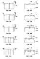
- FIGS. 6A-13Dshow a single crystal silicon wafer at various stages in a fabrication process according to one embodiment of the present invention.
- FIG. 6Ais a plan view of a single crystal silicon wafer according to an embodiment of the present invention.
- FIG. 6Bis a cross-sectional view of the same single crystal silicon wafer taken along line 6 B- 6 B of FIG. 6A .
- FIG. 7Ais a plan view of a single crystal silicon wafer according to an embodiment of the present invention.
- FIG. 7Bis a cross-sectional view of the same single crystal silicon wafer taken along line 7 B- 7 B of FIG. 7A .
- FIG. 8Ais a plan view of a single crystal silicon wafer according to an embodiment of the present invention.
- FIG. 8Bis a cross-sectional view of the same single crystal silicon wafer taken along line 8 B- 8 B of FIG. 8A .
- FIG. 9Ais a plan view of a single crystal silicon wafer according to an embodiment of the present invention.
- FIG. 9Bis a cross-sectional view of the same single crystal silicon wafer taken along line 9 B- 9 B of FIG. 9A .
- FIG. 10Ais a plan view of a single crystal silicon wafer according to an embodiment of the present invention.
- FIG. 10Bis a cross-sectional view of the same single crystal silicon wafer taken along line 10 B- 10 B of FIG. 10A .
- FIG. 11Ais a plan view of a single crystal silicon wafer according to an embodiment of the present invention.
- FIG. 11Bis a cross-sectional view of the same single crystal silicon wafer taken along line 11 B- 11 B of FIG. 11A .
- FIG. 12Ais a plan view of a single crystal silicon wafer according to an embodiment of the present invention.
- FIG. 12Bis a cross-sectional view of the same single crystal silicon wafer taken along line 12 B- 12 B of FIG. 12A .
- FIG. 12Cis a cross-sectional view of the single crystal silicon wafer of FIG. 12A taken along line 12 C- 12 C of FIG. 12A .
- FIG. 13Ais a plan view of a single crystal silicon wafer according to an embodiment of the present invention.
- FIG. 13Bis a cross-sectional view of the same single crystal silicon wafer taken along line 13 B- 13 B of FIG. 13A .
- FIG. 13Cis a cross-sectional view of the single crystal silicon wafer of FIG. 13A taken along line 13 C- 13 C of FIG. 13A .
- FIG. 13Dis a cross-sectional view of the single crystal silicon wafer of FIG. 13A taken along line 13 D- 13 D of FIG. 13A .
- FIGS. 14A-14Eshow a progressive undercut etch of single crystal silicon using a buffered fluoride etch solution of the present invention.
- the top surface of the single crystal siliconrepresents the (100) plane.
- the trenchis ⁇ 110> on the (100) plane.
- FIGS. 15A-15Dshow a progressive undercut etch of single crystal silicon using a buffered fluoride etch solution of the present invention after exposure to NH 4 OH.
- the top surface of the single crystal siliconrepresents the (100) plane.
- the trenchis ⁇ 110> on the (100) plane.
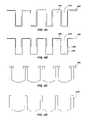
- FIGS. 16A-16Cdepict a time progression for a TMAH etch of (100) silicon.
- FIGS. 17A-17Ishow a method of creating a partial SOI (“PSOI”) DRAM access transistor structure according to an embodiment of the present invention.
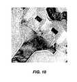
- FIG. 18is a transmission electron micrograph (“TEM”) of a shelf created by a method of the present invention under an integrated DRAM access transistor largely following the method depicted in FIGS. 17A-17I .
- TEMtransmission electron micrograph
- wafer and substrateas used in the following description include any structure having an exposed surface with which to form the integrated circuit (IC) structure of the invention.
- substrateis understood to include semiconductor wafers.
- substrateis also used to refer to semiconductor structures during processing, and may include other layers that have been fabricated thereupon. Both wafer and substrate include doped and undoped semiconductors, epitaxial semiconductor layers supported by a base semiconductor or insulator, as well as other semiconductor structures well known to those of ordinary skill in the art.
- conductoris understood to include semiconductors, and the term “insulator” is defined to include any material that is less electrically conductive than the materials referred to as conductors.
- horizontalas used in this application is defined as a plane parallel to the conventional plane or surface of a wafer or substrate, regardless of the orientation of the wafer or substrate.
- verticalrefers to a direction perpendicular to the horizontal as defined above. Prepositions, such as “on,” “side” (as in “sidewall”), “higher,” “lower,” “over” and “under,” are defined with respect to the conventional plane or surface being on the top surface of the wafer or substrate, regardless of the orientation of the wafer or substrate.
- Etch compositions for oxidizing silicon and etching silicon dioxide to create desired structures according to the present inventionshall be generally described below. With the description as provided below, it will be readily apparent to one skilled in the art that the anisotropic etch compositions described herein may be used in various applications. In other words, the etch compositions may be used whenever silicon etch is being performed and wherein smooth vertical silicon walls or isolated silicon islands are desired. For example, the present invention may be used in the formation of isolation structures for use in the fabrication of integrated circuits.
- the present inventionmay be beneficial in the fabrication of transistor structures, such as pseudo-silicon-on-insulator devices (including DRAM, SRAM, Flash, imagers, PCRAM, MRAM, CAM, etc.), FinFETs, surround gate transistors, as well as MEMS and electro-optical components.
- transistor structuressuch as pseudo-silicon-on-insulator devices (including DRAM, SRAM, Flash, imagers, PCRAM, MRAM, CAM, etc.), FinFETs, surround gate transistors, as well as MEMS and electro-optical components.
- the wet etch chemistry of the present inventionmay be used to fabricate devices that have previously been prohibitively expensive, complicated and/or poor yielding.
- vertical wall devicesmay be manufactured according to an embodiment of the invention.
- the processmay utilize silicon having conventional shallow trench isolation (STI) structures therein.
- the substrateis exposed to a wet anisotropic etchant that undercuts the silicon to create a smooth vertical silicon wall.
- Exemplary etchant solutionsinclude, but are not limited to, buffered oxide etchant (“BOE”) dilute TMAH, TMAH with FX (where “X” is a cation), TMAH with NH 4 F, NH 4 OH, and NH 4 OH with NH 4 F.
- BOEbuffered oxide etchant
- TMAHTMAH with FX (where “X” is a cation)
- TMAH with NH 4 FNH 4 OH
- NH 4 OHNH 4 OH
- NH 4 OHNH 4 OH
- isolated single crystal silicon islandsmay be formed by, generally, undercutting silicon using etchants of the present invention, potential trench fill (e.g., spin-on dielectric or “SOD”) and oxidation of the remaining supporting silicon walls.
- SODspin-on dielectric
- the etchmay be allowed to progress longer than when creating vertical silicon walls such that the underlying “silicon leg” is too narrow for further processing to create a FIN structure.
- This methodprovides an inexpensive alternative to prefabricated silicon-on-insulator substrates that are commercially available.
- One benefit of the isolated single crystal silicon islands of the present inventionis that device performance should not be significantly affected by leaking through the silicon material thereunder because of the oxide underlying the isolated single crystal silicon islands.
- Exemplary etch solutionsinclude hydroxide and hydroxide and fluoride solutions.
- Exemplary etchantsinclude BOE (i.e., a mixture of a NH 4 F aqueous solution (40% concentrated) and an aqueous solution of HF (49% concentrated)), tetramethylammonium hydroxide (TMAH), TMAH with FX (where “X” is a cation), TMAH with NH 4 F, NH 4 OH, and NH 4 OH with NH 4 F.
- the pHmay be greater than 11, more preferably between pH 12 and pH 13.5.
- a solution including 25% TMAHmay be used with a 40% solution of NH 4 F in a ratio between about 4:1 to about 8:1 TMAH:NH 4 F from 9-10 pH to pH 14.5.
- the TMAH and NH 4 F solutionmay be applied to the silicon at a temperature range between 10-100° C., more preferably, 25° C. to 95° C.
- the etching processmay be performed at a temperature in the range of about 10° C. to about 70° C.
- the etching processoccurs at a temperature between 20° C. to about 30° C. and, more preferably, between about 20° C. and 25° C.
- any known methodmay be used to expose the single crystal silicon to the selected etchant.
- the siliconmay be immersed into a tank of the etch solution.
- the solutionmay also be sprayed onto the wafers being etched or may be introduced for contact with the wafer in any other manner, e.g., drip, spraying, vapor, etc.
- FIGS. 1A , 1 B, 2 A, and 2 Bshow a masked single crystal silicon etch performed with different etchant solutions in both the standard silicon orientation ( FIG. 1A and FIG. 2A ) and 45° rotation of the same mask ( FIG. 1B and FIG. 2B ).
- a maskis aligned along the ⁇ 110> directions.
- the ⁇ 111 ⁇ planesdefine the sidewalls, which are sloped from the (100) surface plane.
- the 45° rotationthe mask is aligned along the ⁇ 100> direction and etching is slower in the ⁇ 110> direction.
- the etchantwas dilute NH 4 OH applied at 26° C. and in FIG.
- the etchantwas dilute TMAH applied at 26° C. While the two etchants display different selectivity, both undercut the single crystal silicon 10 and create beveled edges or chamfers 12 . While the beveled edges may be undesirable for some applications, such structures are suitable for further processing to create vertical silicon walls and single crystal silicon islands as further discussed herein.
- etch rate of hydroxide-based etch solutionsi.e., NH 4 OH or TMAH
- vertical wall devicesmay be manufactured having various profiles. It will be appreciated that in some applications, the top portion, or “table top,” of the silicon will be desirable, while in other applications, the profile underneath the silicon will be desirable.
- regular-shaped isolated single crystal silicon islandsmay be formed using a wet etch undercut, potential trench fill (e.g., SOD) and oxidation of the remaining supporting silicon walls.
- potential trench fille.g., SOD
- FIGS. 4A-4Dusing a conventional STI trench as a starting point, vertical silicon walls may be fabricated for devices like FinFETs.
- the silicon active areais undercut to provide better access device isolation. The real estate is improved between the active area and STI structure, resulting in better isolation with the same upper trench width.
- An ideal etchwould provide a horizontal “table top” for transistors and smooth vertical post structure, which has proven difficult using known methods.
- a silicon nitride liner 220may be deposited over the surface of the single crystal silicon 200 and trenches 210 as shown in FIG. 3A .
- a dry etchmay remove the silicon nitride liner 220 from the bottom surface 230 of the trenches 210 and may partially remove the silicon nitride from the sidewalls 240 of trenches 210 as shown in FIG. 3B .
- the etchmay be conducted utilizing a dry anisotropic etching chemistry, with or without plasma, for example, comprising ammonia and at least one fluorocarbon.
- a wet etch using TMAHmay be performed for approximately 5 minutes at 26° C.
- TMAHdeionized water
- TMAHexhibits an etch rate in (100) silicon of approximately 6 ⁇ /second.
- this processcreates “silicon legs” 250 , which may be removed by later processing.
- the etchantis not limited to TMAH, but also includes, but is not limited to, BOE, TMAH with FX (where “X” is a cation), TMAH with NH 4 F, NH 4 OH, and NH 4 OH with NH 4 F.
- TMAHTMAH with FX
- NH 4 FNH 4 F
- NH 4 OHNH 4 OH
- NH 4 OHNH 4 OH with NH 4 F.
- Such solutionsmay be applied alone or in combination with a buffered fluoride etch solution.
- the etchWhen creating isolated silicon islands, the etch may be allowed to progress up to 30 minutes or longer, depending on etch rate and initial dimensions such as distance of trenches and trench depth, to narrow the width of the silicon legs 250 . This is especially effective when the etchant etches faster in a direction parallel to the top surface of the silicon.
- oxide spacersrather than nitride spacers, may be used.
- An SOD fill and oxidation/steam densificationmay then be performed, which removes the silicon legs (or pillars) 250 and creates horizontal isolated silicon island structures 200 ′ as shown in FIG. 3D .
- the isolated silicon island structures 200 ′may then be subject to further processing and incorporated into any desired component including, without limitation, transistors, capacitors, flash devices, DRAM or FLASH memories.
- isolated silicon island structuresare created by extending a spacer the entire length of the trench sidewall followed by oxidation of the entire structure. This process creates a significant stress that may lead to leakage.
- the single crystal silicon 200 aboveremains high quality and unstressed.
- one advantage of the isolated silicon island structures 200 ′ of the present inventionis that device performance would not be significantly affected by leakage through the silicon material thereunder.
- a continued goal of FinFET fabricationis to narrow the dimension of the Fins. If the Fin is thin enough, when a gate is turned on a transistor, it may be possible to completely deplete that portion of the FinFET, providing the user with complete control of the transistor.
- a method of forming Fins according to the present inventionis shown in FIGS. 4A-4D . Starting with a conventional STI trench 210 in single crystal silicon 200 , a silicon nitride liner 220 may be deposited over the surface of the single crystal silicon 200 and trench 210 as shown in FIG. 4A .
- a dry etchmay remove the silicon nitride liner 220 from the bottom surface 230 of the trenches 210 and may partially remove the silicon nitride from the sidewalls 240 of trench 210 as shown in FIG. 4B .
- the etchmay be conducted utilizing a dry anisotropic etching chemistry, with or without plasma, for example, comprising ammonia and at least one fluorocarbon.
- a patternis aligned along the ⁇ 100> direction and a wet etch with TMAH for approximately 4 minutes at 26° C. may be performed to undercut the silicon.
- the etch timemay typically be shorter than when creating single crystal silicon islands as described with respect to FIGS. 3A-3D .
- the trench and spacermay be too deep for narrow FIN structures.
- the etchantis not limited to TMAH, but also includes, but is not limited to, the buffered fluoride etch solution of the present invention, BOE, TMAH with FX (where “X” is a cation), TMAH with NH 4 F, NH 4 OH, and NH 4 OH with NH 4 F.
- a buffered fluoride etch solutionis encompassed by the present invention. Comparing FIGS.
- the etch selectivity of TMAHis shown to be particularly suited for creation of vertical walls, with trench lines that are 45° angles to the vertical (notch-strike) axis on a ⁇ 100> silicon wafer, while the etch selectivity of NH 4 OH is shown to be particularly well suited for creation of isolated silicon islands with an angled sidewall and deeper silicon undercut.
- a hydroxideis selected as the etchant, oxide spacers, rather than nitride spacers, may be used.
- the NH 4 OHprogresses to a diamond shape faster than TMAH because of the higher selectivity of NH 4 OH to (111) silicon as compared to (100) and (110) silicon.
- the choice of etchantmay depend upon the desired final shape and controllability.
- a wet nitride stripmay be performed to create isolated vertical structures, or Fins, 200 ′′ as shown in FIG. 4C .
- the isolated vertical structures, or Fins, 200 ′′may be subjected to further processing as desired.
- Creation and removal of the silicon nitride liner 220may be performed by conventional techniques, as shown in FIG. 4D .
- Oxide spacersmay be used instead of the silicon nitride liner and 220 may be formed by TEOS deposition or SiO 2 growth as known in the art.
- the oxide spacersmay be removed by conventional techniques, such as dilute HF.
- FIGS. 16A-16Fdepict a time progression for both TMAH ( FIGS. 16A-16C ) and NH 4 OH ( FIGS. 16D-16F ).
- the top surface 512 of the single crystal silicon 500represents the (100) plane.
- the trench 510is ⁇ 110> on the (100) plane.
- Both etcheswere performed by immersing (100) silicon in an etchant at 26° C.
- the NH 4 OH etchwas performed using 0.3% NH 4 OH and the TMAH etch was performed using 0.23% TMAH.
- FIGS. 16A and 16Ddepict the etch after 1 minute has elapsed.
- FIGS. 16B and 16Edepict the etch after 2 minutes have elapsed.
- 16C and 16Fdepict the etch after 4 minutes have elapsed.
- the initial shape createdis dependent on the selectivity ratio of the silicon plane.
- a TMAH etchmay achieve the diamond shape shown in FIG. 16F , however, the etch proceeds at a slower rate.
- TMAHallows for more controlled shelf progression.
- a sequential etchmay be performed to customize the desired final shape of the silicon shelf.
- Fins, silicon “table tops” supported by narrow Fins and isolated silicon structuresmay be fabricated at the same time on the same wafer.
- a silicon nitride liner 220may be deposited over the surface of the single crystal silicon 200 and trenches 210 as shown in FIG. 3A .
- a dry etchmay remove the silicon nitride liner 220 from the bottom surface 230 of the trenches 210 and may partially remove the silicon nitride from the sidewalls 240 of trenches 210 as shown in FIG. 3B .
- a wet etch using, for example, TMAHmay be applied to the entire wafer.
- the portion of the wafer to include vertical silicon wallsmay be allowed to proceed with the wet etch for approximately 4 minutes at 26° C. and a wet nitride strip may be performed on that portion of the wafer to create isolated vertical structures, or Fins 200 ′′, as shown in FIG. 4D .
- the portion of the wafer to include single crystal silicon islandsmay be allowed to proceed with the wet etch for a longer period of time, for example, 5-30 minutes at 26° C. to create “silicon legs” 250 as shown in FIG. 3C .
- An SOD fill and oxidation/steam densificationmay then be performed that removes the silicon legs (or pillars) 250 and creates horizontal isolated silicon island structures 200 ′ as shown in FIG. 3D .
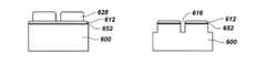
- FIGS. 17A-17Idepict a method of forming a PSOI structure on (100) silicon 600 according to one embodiment of the present invention.
- a resist 628is patterned for the PSOI structure over a hardmask of 500 ⁇ SiN 4 612 , 95 ⁇ SiO 2 652 .
- the patternis dry etched using conventional methods to a desired depth into the silicon 600 followed by conventional wafer cleanup to form at least one trench 616 ( FIG. 17B ).
- the initial dry etchsets the spacer depth 662 ( FIG. 17D ), which may be selected based upon the selectivity and etch rate of the anticipated wet etch.
- the width of the initial openingmay influence the etch and depth of a dry etch.
- a thin layer of SiO 2 652may be grown by dry oxidation of silicon 600 , deposition of approximately 100 ⁇ TEOS SiO 2 followed with an oxide spacer etch to create spacers on the sidewalls 630 of trench 616 ( FIG. 17C ). A subsequent silicon etch is performed within trench 616 to open the desired silicon planes prior to wet etch. The spacer depth 662 correlates to the size of the final shelf of Si 672 ( FIGS. 17D and 17I ).
- a wet etchantmay be selected based on the desired cavity shape and shape of the final shelf 672 .
- NH 4 OHwill progress to a diamond shape faster than TMAH.
- the speed at which an etchant attacks the cornersis selectivity dependent.
- the choice of etchantmay also influence the size of the final shelf 672 .
- FIG. 17Edepicts an NH 4 OH etch after 2 minutes.
- FIG. 17Fdepicts the NH 4 OH etch after 4 minutes.
- the slowest etch planes (111)merge to point 650 .
- the distance to mergeis set by the post-spacer etch 660 depth 660 while the final ledge thickness is shown at 664 .
- the hydroxide etch rate undercutslows in a ⁇ 100> direction with further hydroxide cut after the slow planes meet at point 650 . This may occur with a hydroxide etch after approximately 8 minutes in the example depicted in FIGS. 17A-17I .
- the processmay be essentially self-limiting and the etch profile may stop.
- a second etchant with different selectivitymay be selected to etch, for example, the corners 651 .
- a buffered fluoride etch solution(a volumetric ratio of NH 4 F:QEII:H 2 O 2 of about 4:2:3) etches (111) silicon faster than (100) silicon.
- the undercut profilebecomes more square which may be desirable for some structures including, for example, a PSOI structure.
- the profile shown in FIG. 17Hcorrelates to the TEM depicted in FIG. 18 . If the buffered fluoride etch solution is allowed to progress, the profile may continue to become more square with a slow change of the stem 670 and shelf 672 thickness in the example depicted in FIGS. 17A-17I . ( FIG. 17I ).
- the shape and size of the final productmay be achieved.
- the inventionmay further be understood by the following non-limiting examples.
- a single crystal silicon waferwas etched with NH 4 F 40% volume in water for 5 minutes at 26° C.
- the NH 4 Fundercut the silicon to create a structure suitable for further processing to create either vertical silicon walls or single crystal silicon islands.
- a single crystal silicon waferwas etched with HF and NH 4 F in isopropyl alcohol for 5 minutes at 26° C.
- the HF and NH 4 Fundercut the silicon to create a structure suitable for further processing to create either vertical silicon walls or single crystal silicon islands.
- a single crystal silicon waferwas etched with QEII (HF/H 3 PO 4 :NH 4 F) for 5 minutes at 26° C.
- the QEIIundercut the silicon to create a structure suitable for further processing to create either vertical silicon walls or single crystal silicon islands.
- a single crystal silicon waferwas etched with 100:1 BOE and 150:1 BOE (HF:NH 4 F) for 5 minutes at 26° C.
- the BOEundercut the silicon to create a structure suitable for further processing to create either vertical silicon walls or single crystal silicon islands.
- a single crystal silicon waferwas etched with 0.3% NH 4 OH for 4 minutes at 26° C. The silicon was patterned along the ⁇ 100> direction.
- a second single crystal silicon waferwas etched with 0.23% TMAH for 4 minutes at 26° C. Both etchants undercut silicon; however, there was a significant difference between the etchant selectivity toward different crystal orientation.
- TMAHhas a lower ⁇ 100>: ⁇ 110> etch ratio, which may result in better controlled etching.
- a single crystal silicon waferwas etched with NH 4 OH and NH 4 F for 5 minutes at 26° C.
- the NH 4 OH and NH 4 Fundercut the silicon to create a structure suitable for further processing to create either vertical silicon walls or single crystal silicon islands.
- a single crystal silicon waferwas etched with TMAH and NH 4 F for 5 minutes at 26° C.
- the TMAH and NH 4 Fundercut the silicon to create a structure suitable for further processing to create either vertical silicon walls or single crystal silicon islands.
- the present inventionalso encompasses use of a buffered fluoride etch composition in undercutting single crystal silicon to form vertical structures or isolated silicon islands, the buffered etch solution generally including a fluoride component, an inorganic acid and an oxidizing agent.
- the buffered fluoride etch solutionmay be used alone or in combination with the hydroxide etchants disclosed herein.
- the fluoride componentmay be, without limitation, HF, HF 2 ⁇ , NH 4 F, or TMAF.
- the ammonium fluoridemay be formed with a mixture of ammonium hydroxide and HF.
- the fluoride component or solutionis such that when the reaction of the etch composition with silicon forms silicon dioxide, the fluoride component or solution dissolves away the silicon dioxide formed thereby.
- the fluoride componentmay be present in the amount of 0.5-50% by weight.
- the oxidizing agent of the buffered fluoride etch compositionmay be any oxidizing agent, such as hydrogen peroxide or ozone.
- the oxidizing agentis hydrogen peroxide.
- the inorganic acid componentmay include at least one acid selected from hydrofluoric acid (HF), phosphoric acid (H 3 PO 4 ), sulfuric acid (H 2 SO 4 ), nitric acid (HNO 3 ), hydrochloric acid (HCl), carbonic acid (H 2 CO 3 ), or any other suitable inorganic acid. It is currently preferred that the inorganic acid is H 3 PO 4 . Inorganic acids are commercially available as concentrated solutions (X), which then typically are diluted to a desired concentration (H 2 O:X).
- HClis 37% by weight in deionized water
- HNO 3is 70% by weight in deionized water
- H 2 SO 4is 96% by weight in deionized water
- H 3 PO 4is 85% by weight in deionized water.
- Concentrations of etch compositions described hereinare given based on commercially available solutions. For example, if the etch composition has a concentration of 30% HCl, then the solution includes 30% by weight of the commercially available HCl solution.
- Hydrogen peroxide (H 2 O 2 )is also commercially available as a concentrated solution of approximately 29% by weight in deionized water.
- ammonium fluorideis also commercially available as a concentrated solution of approximately 40% by weight in deionized water. Further, one will recognize that multiple components of the solution may be provided from commercially available solutions. For example, QEII available from Olin Microelectronics Materials (Norwalk, Conn.) provides both NH 4 F and an inorganic acid that may be used to adjust the pH of the solution.
- the buffered fluoride etch solutionpreferably has a pH in the range of about 5.0 to about 9.0. More preferably, the buffered fluoride etch composition has a pH of about 7.8.
- the buffered fluoride etch compositionincludes a fluoride component in a range of about 0.5% to about 50% by weight of the buffered fluoride etch composition, an oxidizing agent in the range of about 0.5% to about 30% by weight of the buffered fluoride etch composition, and an inorganic acid in the range of about 0.1-2% by weight.
- the buffered fluoride etch compositionmay preferably include a volumetric ratio of NH 4 F:QEII:H 2 O 2 of about 4:2:3 (or approximately 10-35 w % NH 4 F, approximately 3-20 w % H 2 O 2 , approximately 0.1-2 w % H 3 PO 4 or other acid, and the remaining balance of deionized water).
- the ionic strength of the buffered fluoride etch compositionis greater than one; more preferably, the ionic strength is in the range of about 5 to about 20.
- ionic strengthrefers to a measure of the average electrostatic interaction among ions in the composition, which is equal to one-half the sum of the terms obtained by multiplying the molarity of each ion by its valence squared.
- the redox potential of the etch compositionis in the range of about ⁇ 0.5 to about +0.7 or higher (vs. Standard Hydrogen Electrode (SHE)).
- SHEStandard Hydrogen Electrode
- the redox potentialis a measure of the effectiveness of the etch composition as an oxidizing agent, i.e., the ability of the etch composition to oxidize silicon for removal by the HF component of the etch composition.
- buffered fluoride etch solutionis particularly applicable to the use of ammonium fluoride and hydrogen peroxide but appear to be equally applicable to buffered fluoride etch compositions having other combinations of components as described above, such as when ammonium fluoride is provided by ammonium hydroxide and hydrofluoric acid.
- suitable amounts of ammonium hydroxide and hydrofluoric acidmay be mixed to provide an adequate amount of ammonium fluoride.
- ozoneis preferably present in a range of about 1 part per million (ppm) to about 50 ppm.
- the buffered fluoride etch solutionmay exhibit an etch rate of silicon that is greater than three times the etch rate of an oxide being exposed to the same etch composition, i.e., the selectivity between silicon and oxide is greater than 3. More preferably, the selectivity between silicon and oxide using the etch composition is greater than 6 of oxide versus (100) silicon. Similarly, the buffered fluoride etch solution may exhibit Si 3 N 4 selectivity for (110) silicon between about 10 to 80.
- the etch rate for silicon using the etch compositionis preferably greater than about 150 ⁇ /minute if the etch rate selectivity can be maintained. An etch rate that is too slow or too fast may result in a non-uniform end product.
- the etch compositionis such that after removal of silicon using the etch composition the silicon surface has a desired surface roughness adequate for later processing.
- the roughness of the silicon surface following the etchis within the range of about 1.25 ⁇ RMS to about 1.30 ⁇ RMS.
- the silicon surfacemay desirably fall within such a range for roughness after more than 180 ⁇ of silicon is removed.
- RMS roughnessmay be determined by Atomic Force Microscopy (AFM), which scans a surface area of about 1 ⁇ m 2 and gives an average peak-to-valley measurement across this 1 ⁇ m 2 surface area.
- AFMAtomic Force Microscopy
- the high selectivity to oxide as described aboveis a high selectivity to thermal oxide.
- thermal oxidemay be formed by thermal oxidation such as with use of a wet or dry furnace oxidation.
- selectivityis also applicable to oxides formed by chemical vapor deposition (CVD), such as high-density plasma oxide typically used in isolation processes, such as shallow trench isolation.
- CVDchemical vapor deposition
- any known methodmay be used to expose the single crystal silicon to the selected etchant.
- the siliconmay be immersed into a tank of the etch solution.
- the solutionmay also be sprayed onto the wafers being etched or may be introduced for contact with the wafer in any other manner, e.g., drip, spraying, vapor, etc.
- the etching processmay be performed at a temperature in the range of about 10° C. to about 90° C.
- the etching processoccurs at a temperature between 10° C. to about 30° C. and, more preferably, between about 22° C. and 25° C.
- a single crystal silicon 10 undercutwas performed in both the standard silicon orientation (i.e., patterned along the ⁇ 110> direction) and 45° rotation in (100) silicon using a buffered fluoride etch solution (10 L NH 4 F+5 L QEII+7.5 L H 2 O 2 ) at 26° C. according to the present invention.
- the buffered fluoride etch solution used in FIG. 5Ademonstrates that the (100) silicon planes is the slow etching planes taht allows the creation of square undercuts if the pattern is aligned along the ⁇ 100> direction.
- the (111) planeis a slow etch; thus, it was surprising to discover a wet etch with a slow plane etch in (100) silicon.
- the buffered fluoride etch solutionprovides good selectivity, smooth surfaces and controllable etching of (100) silicon.
- the lateral shelf 14 and lack of beveled cornersenable the easy creation thereon of electrical devices such as FinFETs, Pseudo-SOI or RAD bowls in conventional CMOS wafers that are manufactured on (100) silicon.
- FIG. 18is a TEM of a silicon shelf built under a transistor following the method described in association with FIGS. 17A-17I .
- the use of the buffered fluoride etch solutionalso creates concave square corners without a lateral spacer, which is desirable for electronic properties in silicon fingers of sheets that have very different properties from the adjacent material having no material etched.
- the concave square corners depicted in FIG. 3Cmay also be useful for a discrete change in device mechanical and optical properties when fabricating MEMS.
- the concave corner in (100) siliconalso allows simple integration in CMOS devices and enables MEMS mechanical and optical structures to be integrated with CMOS processing more easily.
- the ⁇ 110> directional etchis approximately two and one half times higher than (100
- FIGS. 6A-13Ddepict a partial process for creating a pseudo-SOI structure according to a method of the present invention.
- part Ashows a plan view of the structure and part B shows a cross-sectional view of the corresponding structure taken along B-B.
- FIGS. 6A and 6Bdepict a single crystal silicon substrate 100 .
- a silicon nitride liner 112is formed thereover.
- a masking layer 128is formed over the silicon nitride liner 112 as known in the art.
- the masking layer 128may be patterned to form at least one trench mask opening 132 .
- Conventional photolithography or other lithographic or non-lithographic methods, regardless of the presence of the masking layer 128are also contemplated.
- the silicon nitride liner 112 and single crystal silicon substrate 100are etched through the mask opening 132 to form at least one trench 116 within the single crystal silicon substrate 100 .
- the etchmay be conducted utilizing a dry anisotropic etching chemistry, with or without plasma, for example, comprising ammonia and at least one fluorocarbon.
- Masking layer 128may remain or may be removed when etching into the single crystal silicon substrate 100 . While a specific method of forming trench 116 has been disclosed, it will be understood by one of skill in the art that any method of forming trench 116 may be utilized.
- a nitride layermay be deposited over the silicon nitride liner 112 and trench 116 followed by an etch taht removes the nitride from the bottom 126 of the trench 116 , but creates nitride spacers 118 on the sidewalls 130 of trench 116 .
- Creation of the Si 3 N 4 linermay be performed by conventional techniques. Oxide spacers may also be used by TEOS deposition or SiO 2 growth as known in the art.
- the buffered fluoride etch solution of the present inventionmay then be applied to undercut the single crystal silicon substrate 100 .
- the buffered fluoride etch solutionmay be applied at approximately 23° C. for approximately 5 minutes, depending on the desired size of the lateral shelf 114 .
- the buffered fluoride etch solutionetches faster in a direction parallel to the single crystal silicon substrate 100 as compared with the vertical etch through the bottom 126 of the trench 116 .
- a lateral shelf 114 having a thickness of approximately 450 ⁇ to 550 ⁇may be created as shown in FIG. 9B .
- a nitride liner 120may be deposited on the bottom 126 and sidewalls 130 of the trench 116 and then the trench 116 may be filled with an oxide material 122 , for example, an SOD as shown in FIGS. 10A and 10B .
- a mask 124is deposited and patterned over the silicon nitride liner 112 and oxide material 122 .
- a conventional silicon etch having some selectivity to oxidemay be performed as shown in FIGS. 11A , 11 B, and 12 A- 12 C.
- An optional nitride liner 136may be deposited and an SOD fill may be performed as shown in FIGS. 13A-13D .
- the structure 150may be subjected to further processing to form, for example, transistors, capacitors and digit lines thereover to complete the pseudo-SOI structure.
- the structure 150includes a lateral shelf 114 having a thickness of about 500 ⁇ (+/ ⁇ 10%).
- structure 150including any transistors, such as ray transistors or access transistors, overlying structure 150 has significantly lower leakage due to the presence of oxide material 122 underlying the silicon (see, e.g., FIG. 13B ). It will be understood that structure 150 is not limited to being an intermediate pseudo-SOI structure. Any number of additional fabrication steps may be performed in conjunction with the present invention to create any desired device.
- FIGS. 14A-14Edepict silicon oxidation and etching by immersion at 23° C. using a solution including NH 4 F, QEII and H 2 O 2 (provided in a ratio of 4:2:3 by volume).
- FIG. 14Adepicts a trench 310 in single crystal silicon 300 with a nitride liner 320 prior to addition of the buffered fluoride etch solution of the present invention.
- the top surface 312 of the single crystal silicon 300represents the (100) plane.
- the trench 310is ⁇ 110> on the (100) plane.
- an undercut profileis visible having a lateral shelf 314 ( FIG. 14B ).
- the etchis progressing faster perpendicular to the (100) direction (i.e., perpendicular to the STI sidewall), than in the (100) direction (i.e., perpendicular to the wafer surface) as shown in FIGS. 14C-14E after 22 minutes, 25 minutes and 28 minutes exposure, respectively.
- the width of the underlying silicon leg, or pillar, 350decreases with increased exposure to the buffered fluoride etch solution.
- FIGS. 15A-15Ddepict the etch progression of single crystal silicon 400 at 0 minutes ( FIG. 15A ), 3 min ( FIG. 15B ), 6 min ( FIG. 15C ) and 9 min ( FIG. 15D ) exposure by immersion to the buffered fluoride etch solution after a five-minute anisotropic NH 4 OH etch at 23° C.
- the top surface 412 of the single crystal silicon 400represents the (100) plane.
- the trench 410is ⁇ 110> on the (100) plane.
- Increasing the time of the buffered fluoride etch solution etchforms a shelf undercut of the silicon active area without significantly increasing the trench depth.
- the silicon legs, or pillars, 450 under the single crystal silicon 400become increasingly narrow as the etch progresses.
- devicesmay be manufactured having various characteristics. By manipulating the etch time and etchant combination, different undercut profiles may be achieved.
- the buffered fluoride etch solutionmay be sequentially combined with hydroxides, NH 4 OH, NH 4 F, TMAH or combinations thereof.
- a single crystal silicon waferwas etched with NH 4 F, QEII and H 2 O 2 (provided in a ratio of 4:2:3) for 5 minutes at 26° C.
- the siliconwas patterned along the ⁇ 100> direction.
- the etchantcreated a square undercut in the single crystal silicon wafer.
Landscapes
- Engineering & Computer Science (AREA)
- Computer Hardware Design (AREA)
- Power Engineering (AREA)
- Microelectronics & Electronic Packaging (AREA)
- Physics & Mathematics (AREA)
- Manufacturing & Machinery (AREA)
- Condensed Matter Physics & Semiconductors (AREA)
- General Physics & Mathematics (AREA)
- Chemical & Material Sciences (AREA)
- Chemical Kinetics & Catalysis (AREA)
- General Chemical & Material Sciences (AREA)
- Inorganic Chemistry (AREA)
- Weting (AREA)
- Element Separation (AREA)
- Semiconductor Memories (AREA)
Abstract
Description
Si+6OH−

SiO2+4H++4e−
Sis+2OH−
═Si(OH)2
Si+4H+4e−
Si+2H2O2=H2SiO3+H2O=SiO2+2H2O (6)
Half-cell reduction/oxidation reactions:
H2O2+2H++2e−
Sis+2OH−
H2SiO3+6HF
The typical selectivity between (100) silicon crystal orientation and thermal oxide is approximately 6 using NH4F, QEII and H2O2(provided in a ratio of 4:2:3) while the etchant selectivity of 100:1 deionized water:TMAH is approximately or larger than 1000. The <110> directional etch is approximately two and one half times higher than (100) silicon etch.
Claims (35)
Priority Applications (4)
| Application Number | Priority Date | Filing Date | Title |
|---|---|---|---|
| US11/445,544US7709341B2 (en) | 2006-06-02 | 2006-06-02 | Methods of shaping vertical single crystal silicon walls and resulting structures |
| US12/687,619US8159050B2 (en) | 2006-06-02 | 2010-01-14 | Single crystal silicon structures |
| US13/416,834US9040424B2 (en) | 2006-06-02 | 2012-03-09 | Methods of forming single crystal silicon structures and semiconductor device structures including single crystal silicon structures |
| US14/676,338US20150206761A1 (en) | 2006-06-02 | 2015-04-01 | Methods of forming single crystal silicon structures |
Applications Claiming Priority (1)
| Application Number | Priority Date | Filing Date | Title |
|---|---|---|---|
| US11/445,544US7709341B2 (en) | 2006-06-02 | 2006-06-02 | Methods of shaping vertical single crystal silicon walls and resulting structures |
Related Child Applications (1)
| Application Number | Title | Priority Date | Filing Date |
|---|---|---|---|
| US12/687,619DivisionUS8159050B2 (en) | 2006-06-02 | 2010-01-14 | Single crystal silicon structures |
Publications (2)
| Publication Number | Publication Date |
|---|---|
| US20070281493A1 US20070281493A1 (en) | 2007-12-06 |
| US7709341B2true US7709341B2 (en) | 2010-05-04 |
Family
ID=38790801
Family Applications (4)
| Application Number | Title | Priority Date | Filing Date |
|---|---|---|---|
| US11/445,544ActiveUS7709341B2 (en) | 2006-06-02 | 2006-06-02 | Methods of shaping vertical single crystal silicon walls and resulting structures |
| US12/687,619ActiveUS8159050B2 (en) | 2006-06-02 | 2010-01-14 | Single crystal silicon structures |
| US13/416,834Active2027-04-04US9040424B2 (en) | 2006-06-02 | 2012-03-09 | Methods of forming single crystal silicon structures and semiconductor device structures including single crystal silicon structures |
| US14/676,338AbandonedUS20150206761A1 (en) | 2006-06-02 | 2015-04-01 | Methods of forming single crystal silicon structures |
Family Applications After (3)
| Application Number | Title | Priority Date | Filing Date |
|---|---|---|---|
| US12/687,619ActiveUS8159050B2 (en) | 2006-06-02 | 2010-01-14 | Single crystal silicon structures |
| US13/416,834Active2027-04-04US9040424B2 (en) | 2006-06-02 | 2012-03-09 | Methods of forming single crystal silicon structures and semiconductor device structures including single crystal silicon structures |
| US14/676,338AbandonedUS20150206761A1 (en) | 2006-06-02 | 2015-04-01 | Methods of forming single crystal silicon structures |
Country Status (1)
| Country | Link |
|---|---|
| US (4) | US7709341B2 (en) |
Cited By (14)
| Publication number | Priority date | Publication date | Assignee | Title |
|---|---|---|---|---|
| US20080187463A1 (en)* | 2007-02-07 | 2008-08-07 | Wells David H | Electromagnetic radiation interaction components, fluorimetry systems, semiconductor constructions, and electromagnetic radiation emitter and conduit construction |
| US20080187719A1 (en)* | 2006-11-17 | 2008-08-07 | Fuji Electric Device Technology Co., Ltd. | Nano-imprinting mold, method of manufacture of nano-imprinting mold, and recording medium manufactured with nano-imprinting mold |
| US20080296588A1 (en)* | 2007-06-01 | 2008-12-04 | Hugo Optotech Inc. | Semiconductor substrate with electromagnetic-wave-scribed nicks, semiconductor light-emitting device with such semiconductor substrate and manufacture thereof |
| US20090236666A1 (en)* | 2006-08-18 | 2009-09-24 | Micron Technology, Inc. | Integrated Circuitry |
| US20120021204A1 (en)* | 2010-07-26 | 2012-01-26 | International Business Machines Corporation | Structure and method to form nanopore |
| US20120086053A1 (en)* | 2010-10-08 | 2012-04-12 | Taiwan Semiconductor Manufacturing Company, Ltd. | Transistor having notched fin structure and method of making the same |
| US20120153469A1 (en)* | 2010-01-12 | 2012-06-21 | Maxchip Electronics Corp. | Micro electronic mechanical system structure |
| US8450214B2 (en) | 2006-06-02 | 2013-05-28 | Micron Technology, Inc. | Methods of etching single crystal silicon |
| US9040424B2 (en) | 2006-06-02 | 2015-05-26 | Micron Technology, Inc. | Methods of forming single crystal silicon structures and semiconductor device structures including single crystal silicon structures |
| US9111853B2 (en) | 2013-03-15 | 2015-08-18 | Micron Technology, Inc. | Methods of forming doped elements of semiconductor device structures |
| US9219068B2 (en)* | 2013-01-09 | 2015-12-22 | Globalfoundries Inc | FinFET with dielectric isolation by silicon-on-nothing and method of fabrication |
| US9318392B1 (en)* | 2015-06-18 | 2016-04-19 | International Business Machines Corporation | Method to form SOI fins on a bulk substrate with suspended anchoring |
| US10153358B2 (en) | 2016-02-17 | 2018-12-11 | Samsung Electronics Co., Ltd. | Semiconductor device and method for manufacturing the same |
| US20210375668A1 (en)* | 2020-05-28 | 2021-12-02 | Imec Vzw | Method for producing an undercut in a 300 mm silicon-on-insulator platform |
Families Citing this family (60)
| Publication number | Priority date | Publication date | Assignee | Title |
|---|---|---|---|---|
| DE102006002753B4 (en)* | 2006-01-20 | 2010-09-30 | X-Fab Semiconductor Foundries Ag | Method and apparatus for evaluating the undercut of deep trench structures in SOI slices |
| US7625776B2 (en)* | 2006-06-02 | 2009-12-01 | Micron Technology, Inc. | Methods of fabricating intermediate semiconductor structures by selectively etching pockets of implanted silicon |
| US8852851B2 (en) | 2006-07-10 | 2014-10-07 | Micron Technology, Inc. | Pitch reduction technology using alternating spacer depositions during the formation of a semiconductor device and systems including same |
| US7498265B2 (en) | 2006-10-04 | 2009-03-03 | Micron Technology, Inc. | Epitaxial silicon growth |
| US20080124874A1 (en)* | 2006-11-03 | 2008-05-29 | Samsung Electronics Co., Ltd. | Methods of Forming Field Effect Transistors Having Silicon-Germanium Source and Drain Regions |
| TW200901368A (en)* | 2007-06-23 | 2009-01-01 | Promos Technologies Inc | Shallow trench isolation structure and method for forming thereof |
| JP2009231595A (en)* | 2008-03-24 | 2009-10-08 | Oki Data Corp | Method of manufacturing semiconductor device |
| CN102084467A (en) | 2008-04-14 | 2011-06-01 | 班德加普工程有限公司 | Process for fabricating nanowire arrays |
| US8226840B2 (en) | 2008-05-02 | 2012-07-24 | Micron Technology, Inc. | Methods of removing silicon dioxide |
| US7989307B2 (en) | 2008-05-05 | 2011-08-02 | Micron Technology, Inc. | Methods of forming isolated active areas, trenches, and conductive lines in semiconductor structures and semiconductor structures including the same |
| US10151981B2 (en)* | 2008-05-22 | 2018-12-11 | Micron Technology, Inc. | Methods of forming structures supported by semiconductor substrates |
| DE102008040597A1 (en)* | 2008-07-22 | 2010-01-28 | Robert Bosch Gmbh | Micromechanical component with back volume |
| US8247302B2 (en) | 2008-12-04 | 2012-08-21 | Micron Technology, Inc. | Methods of fabricating substrates |
| US8796155B2 (en) | 2008-12-04 | 2014-08-05 | Micron Technology, Inc. | Methods of fabricating substrates |
| US8273634B2 (en) | 2008-12-04 | 2012-09-25 | Micron Technology, Inc. | Methods of fabricating substrates |
| US8268543B2 (en) | 2009-03-23 | 2012-09-18 | Micron Technology, Inc. | Methods of forming patterns on substrates |
| US9330934B2 (en) | 2009-05-18 | 2016-05-03 | Micron Technology, Inc. | Methods of forming patterns on substrates |
| TWI373450B (en) | 2009-07-29 | 2012-10-01 | Pixart Imaging Inc | Microelectronic device and method for fabricating mems resonator thereof |
| KR101640830B1 (en)* | 2009-08-17 | 2016-07-22 | 삼성전자주식회사 | Substrate structure and manufacturing method of the same |
| US8603848B2 (en)* | 2009-08-25 | 2013-12-10 | Electronics And Telecommunications Research Institute | Three-dimensional MEMS structure and method of manufacturing the same |
| US8455859B2 (en) | 2009-10-01 | 2013-06-04 | Taiwan Semiconductor Manufacturing Company, Ltd. | Strained structure of semiconductor device |
| US8765556B2 (en)* | 2009-12-23 | 2014-07-01 | Taiwan Semiconductor Manufacturing Company, Ltd. | Method of fabricating strained structure in semiconductor device |
| US8357601B2 (en) | 2010-02-09 | 2013-01-22 | Micron Technology, Inc. | Cross-hair cell wordline formation |
| US8674472B2 (en) | 2010-08-10 | 2014-03-18 | International Business Machines Corporation | Low harmonic RF switch in SOI |
| US8518788B2 (en) | 2010-08-11 | 2013-08-27 | Micron Technology, Inc. | Methods of forming a plurality of capacitors |
| US8455341B2 (en) | 2010-09-02 | 2013-06-04 | Micron Technology, Inc. | Methods of forming features of integrated circuitry |
| CN102479738B (en) | 2010-11-23 | 2014-05-28 | 中国科学院微电子研究所 | Trench isolation structure and forming method thereof |
| US8993451B2 (en) | 2011-04-15 | 2015-03-31 | Freescale Semiconductor, Inc. | Etching trenches in a substrate |
| US8575032B2 (en) | 2011-05-05 | 2013-11-05 | Micron Technology, Inc. | Methods of forming a pattern on a substrate |
| US9076680B2 (en) | 2011-10-18 | 2015-07-07 | Micron Technology, Inc. | Integrated circuitry, methods of forming capacitors, and methods of forming integrated circuitry comprising an array of capacitors and circuitry peripheral to the array |
| CN103107072B (en)* | 2011-11-11 | 2015-11-25 | 中芯国际集成电路制造(上海)有限公司 | A kind of manufacture method of multiple gate field effect transistor device |
| US9323010B2 (en)* | 2012-01-10 | 2016-04-26 | Invensas Corporation | Structures formed using monocrystalline silicon and/or other materials for optical and other applications |
| US9177794B2 (en) | 2012-01-13 | 2015-11-03 | Micron Technology, Inc. | Methods of patterning substrates |
| US9117877B2 (en)* | 2012-01-16 | 2015-08-25 | Globalfoundries Inc. | Methods of forming a dielectric cap layer on a metal gate structure |
| JP5960511B2 (en)* | 2012-06-01 | 2016-08-02 | 東京応化工業株式会社 | Silicon anisotropic etching method |
| US8629048B1 (en) | 2012-07-06 | 2014-01-14 | Micron Technology, Inc. | Methods of forming a pattern on a substrate |
| US9269791B2 (en)* | 2012-07-10 | 2016-02-23 | United Microelectronics Corp. | Multi-gate MOSFET with embedded isolation structures |
| CN103594361A (en)* | 2012-08-13 | 2014-02-19 | 中芯国际集成电路制造(上海)有限公司 | Formation method of semiconductor structure |
| CN103794498B (en)* | 2012-10-29 | 2016-12-21 | 中芯国际集成电路制造(上海)有限公司 | A kind of semiconductor device and preparation method thereof |
| CN103811341B (en)* | 2012-11-09 | 2016-05-11 | 中国科学院微电子研究所 | Semiconductor device and method for manufacturing the same |
| US9768271B2 (en)* | 2013-02-22 | 2017-09-19 | Micron Technology, Inc. | Methods, devices, and systems related to forming semiconductor power devices with a handle substrate |
| US9005458B2 (en)* | 2013-02-26 | 2015-04-14 | Micron Technology, Inc. | Photonic device structure and method of manufacture |
| US9275868B2 (en)* | 2013-07-19 | 2016-03-01 | Globalfoundries Inc. | Uniform roughness on backside of a wafer |
| US20150048422A1 (en)* | 2013-08-16 | 2015-02-19 | International Business Machines Corporation | A method for forming a crystalline compound iii-v material on a single element substrate |
| US9934981B2 (en)* | 2013-09-26 | 2018-04-03 | Varian Semiconductor Equipment Associates, Inc. | Techniques for processing substrates using directional reactive ion etching |
| US9472652B2 (en)* | 2013-12-20 | 2016-10-18 | Taiwan Semiconductor Manufacturing Company, Ltd. | Fin structure of semiconductor device |
| US10008384B2 (en) | 2015-06-25 | 2018-06-26 | Varian Semiconductor Equipment Associates, Inc. | Techniques to engineer nanoscale patterned features using ions |
| US10461152B2 (en)* | 2017-07-10 | 2019-10-29 | Globalfoundries Inc. | Radio frequency switches with air gap structures |
| US10833153B2 (en) | 2017-09-13 | 2020-11-10 | Globalfoundries Inc. | Switch with local silicon on insulator (SOI) and deep trench isolation |
| US10446643B2 (en) | 2018-01-22 | 2019-10-15 | Globalfoundries Inc. | Sealed cavity structures with a planar surface |
| US11037792B2 (en)* | 2018-10-25 | 2021-06-15 | Taiwan Semiconductor Manufacturing Company Ltd. | Semiconductor structure etching solution and method for fabricating a semiconductor structure using the same etching solution |
| US10466514B1 (en)* | 2018-11-06 | 2019-11-05 | Globalfoundries Inc. | Electro-optic modulator with vertically-arranged optical paths |
| US11410872B2 (en) | 2018-11-30 | 2022-08-09 | Globalfoundries U.S. Inc. | Oxidized cavity structures within and under semiconductor devices |
| US10923577B2 (en) | 2019-01-07 | 2021-02-16 | Globalfoundries U.S. Inc. | Cavity structures under shallow trench isolation regions |
| US11112694B2 (en)* | 2019-05-15 | 2021-09-07 | Applied Materials, Inc. | Methods of forming variable-depth device structures |
| US11127816B2 (en) | 2020-02-14 | 2021-09-21 | Globalfoundries U.S. Inc. | Heterojunction bipolar transistors with one or more sealed airgap |
| US11712766B2 (en)* | 2020-05-28 | 2023-08-01 | Toyota Motor Engineering And Manufacturing North America, Inc. | Method of fabricating a microscale canopy wick structure having enhanced capillary pressure and permeability |
| CN111876157A (en)* | 2020-06-30 | 2020-11-03 | 镇江润晶高纯化工科技股份有限公司 | Preparation and etching method of TMAH etching solution |
| US12148625B2 (en) | 2022-09-16 | 2024-11-19 | Tokyo Electron Limited | Methods to prevent surface charge induced cd-dependent etching of material formed within features on a patterned substrate |
| US20240375942A1 (en)* | 2023-05-09 | 2024-11-14 | Calient Technologies, Inc. | Double notch etch to reduce under cut of micro electro-mechanical system (mems) devices |
Citations (40)
| Publication number | Priority date | Publication date | Assignee | Title |
|---|---|---|---|---|
| US4531282A (en) | 1977-04-25 | 1985-07-30 | Nippon Telegraph And Telephone Public Corp. | Bipolar transistors having vertically arrayed collector-base-emitter with novel polycrystalline base electrode surrounding island emitter and method of making same |
| US4891255A (en) | 1988-09-29 | 1990-01-02 | The United States Of America As Represented By The United States Department Of Energy | (110) Oriented silicon wafer latch accelerometer and process for forming the same |
| US5427975A (en)* | 1993-05-10 | 1995-06-27 | Delco Electronics Corporation | Method of micromachining an integrated sensor on the surface of a silicon wafer |
| US5536675A (en) | 1993-12-30 | 1996-07-16 | Intel Corporation | Isolation structure formation for semiconductor circuit fabrication |
| US6100162A (en) | 1999-05-14 | 2000-08-08 | Micron Technology, Inc. | Method of forming a circuitry isolation region within a semiconductive wafer |
| US6245615B1 (en) | 1999-08-31 | 2001-06-12 | Micron Technology, Inc. | Method and apparatus on (110) surfaces of silicon structures with conduction in the <110> direction |
| US6290863B1 (en) | 1999-07-31 | 2001-09-18 | Micron Technology, Inc. | Method and apparatus for etch of a specific subarea of a semiconductor work object |
| US6319333B1 (en) | 1996-11-12 | 2001-11-20 | Micron Technology, Inc. | Silicon-on-insulator islands |
| US20020001968A1 (en) | 1999-08-30 | 2002-01-03 | Whonchee Lee | Compositions for etching silicon with high selectivity to oxides and methods of using same |
| US6339241B1 (en) | 2000-06-23 | 2002-01-15 | International Business Machines Corporation | Structure and process for 6F2 trench capacitor DRAM cell with vertical MOSFET and 3F bitline pitch |
| US20020025636A1 (en) | 1999-10-20 | 2002-02-28 | Dong-Hyuk Ju | Field effect transitor with non-floating body and method for forming same on a bulk silicon wafer |
| US6358861B1 (en)* | 1999-01-13 | 2002-03-19 | Mitsubishi Denki Kabushiki Kaisha | Manufacturing method of silicon device |
| US6465865B1 (en) | 1996-01-05 | 2002-10-15 | Micron Technology, Inc. | Isolated structure and method of fabricating such a structure on a substrate |
| US20030003759A1 (en) | 2001-06-27 | 2003-01-02 | Infineon Technologies North America Corp | Etch selectivity inversion for etching along crystallographic directions in silicon |
| US20030022505A1 (en) | 2001-07-24 | 2003-01-30 | Luc Ouellet | Micro-fluidic devices |
| US6518112B2 (en) | 1998-01-05 | 2003-02-11 | International Business Machines Corporation | High performance, low power vertical integrated CMOS devices |
| US20030057438A1 (en) | 2001-09-24 | 2003-03-27 | Motorola, Inc. | Structure and method for fabricating semiconductor structures and devices utilizing lateral epitaxial overgrowth |
| US6602745B2 (en) | 2000-09-14 | 2003-08-05 | Infineon Technologies North America Corp. | Field effect transistor and method of fabrication |
| US20040014280A1 (en) | 2002-07-22 | 2004-01-22 | Josef Willer | Non-Volatile memory cell and fabrication method |
| US6686214B2 (en) | 2000-12-08 | 2004-02-03 | Dalsa Semiconductor Inc. | Method of aligning a photolithographic mask to a crystal plane |
| US20040038533A1 (en) | 1999-04-09 | 2004-02-26 | Chunlin Liang | Isolated junction structure and method of manufacture |
| US6713341B2 (en) | 2002-02-05 | 2004-03-30 | Nanya Technology Corporation | Method of forming a bottle-shaped trench in a semiconductor substrate |
| US20040067346A1 (en) | 2000-12-19 | 2004-04-08 | Hofmann Wolfgang M. J. | Multiple-level actuators and clamping devices |
| US20040118805A1 (en) | 2002-12-18 | 2004-06-24 | Hareland Scott A. | Pre-etch implantation damage for the removal of thin film layers |
| US6784076B2 (en) | 2002-04-08 | 2004-08-31 | Micron Technology, Inc. | Process for making a silicon-on-insulator ledge by implanting ions from silicon source |
| US6808994B1 (en) | 2003-06-17 | 2004-10-26 | Micron Technology, Inc. | Transistor structures and processes for forming same |
| US20040214436A1 (en) | 2000-02-07 | 2004-10-28 | Dow Daniel B. | Method of fabricating a semiconductor work object |
| US20050020091A1 (en) | 2003-07-22 | 2005-01-27 | Janos Fucsko | Wet etching method of removing silicon from a substrate and method of forming trench isolation |
| US6858903B2 (en) | 2002-11-20 | 2005-02-22 | International Business Machines Corporation | MOSFET device with in-situ doped, raised source and drain structures |
| US6881622B2 (en) | 2002-05-30 | 2005-04-19 | Taiwan Semiconductor Manufacturing Co., Ltd | Aqueous ammonium hydroxide amorphous silicon etch method for forming microelectronic capacitor structure |
| US6902962B2 (en) | 2003-04-04 | 2005-06-07 | Taiwan Semiconductor Manufacturing Company, Ltd. | Silicon-on-insulator chip with multiple crystal orientations |
| US6909147B2 (en) | 2003-05-05 | 2005-06-21 | International Business Machines Corporation | Multi-height FinFETS |
| US6927104B2 (en) | 2003-09-15 | 2005-08-09 | Chartered Semiconductor Manufacturing Ltd. | Method of forming double-gated silicon-on-insulator (SOI) transistors with corner rounding |
| US20050208727A1 (en) | 2004-03-18 | 2005-09-22 | Nanya Technology Corporation | Method of etching bottle trench and fabricating capacitor with same |
| US6960507B2 (en) | 2003-07-24 | 2005-11-01 | Samsung Electronics Co., Ltd. | Vertical double-channel silicon-on-insulator transistor and method of manufacturing the same |
| US6963114B2 (en) | 2003-12-29 | 2005-11-08 | Taiwan Semiconductor Manufacturing Company, Ltd. | SOI MOSFET with multi-sided source/drain silicide |
| US6964903B2 (en) | 1998-09-01 | 2005-11-15 | Micron Technology, Inc. | Method of fabricating a transistor on a substrate to operate as a fully depleted structure |
| US6968110B2 (en) | 2003-04-21 | 2005-11-22 | Sioptical, Inc. | CMOS-compatible integration of silicon-based optical devices with electronic devices |
| US7045407B2 (en)* | 2003-12-30 | 2006-05-16 | Intel Corporation | Amorphous etch stop for the anisotropic etching of substrates |
| US20070173007A1 (en) | 2006-01-23 | 2007-07-26 | Hynix Semiconductor, Inc. | Semiconductor device and method for fabricating the same |
Family Cites Families (20)
| Publication number | Priority date | Publication date | Assignee | Title |
|---|---|---|---|---|
| US4407058A (en)* | 1981-05-22 | 1983-10-04 | International Business Machines Corporation | Method of making dense vertical FET's |
| JPH0414868A (en)* | 1990-05-09 | 1992-01-20 | Hitachi Ltd | Semiconductor memory and manufacture thereof |
| KR970000533B1 (en)* | 1990-12-20 | 1997-01-13 | 후지쓰 가부시끼가이샤 | Eprom with trench in thick field oxide |
| JP3919921B2 (en) | 1997-09-26 | 2007-05-30 | 三菱電機株式会社 | Semiconductor device |
| US6528837B2 (en)* | 1997-10-06 | 2003-03-04 | Micron Technology, Inc. | Circuit and method for an open bit line memory cell with a vertical transistor and trench plate trench capacitor |
| US6066869A (en)* | 1997-10-06 | 2000-05-23 | Micron Technology, Inc. | Circuit and method for a folded bit line memory cell with vertical transistor and trench capacitor |
| US6242775B1 (en)* | 1998-02-24 | 2001-06-05 | Micron Technology, Inc. | Circuits and methods using vertical complementary transistors |
| US6426254B2 (en) | 1999-06-09 | 2002-07-30 | Infineon Technologies Ag | Method for expanding trenches by an anisotropic wet etch |
| TW499729B (en)* | 2001-03-16 | 2002-08-21 | Nanya Technology Corp | Method of improving uniformity of oxide layer around trench sidewall and manufacture method of deep trench capacitor |
| US6805432B1 (en)* | 2001-07-31 | 2004-10-19 | Hewlett-Packard Development Company, L.P. | Fluid ejecting device with fluid feed slot |
| US6841825B2 (en)* | 2002-06-05 | 2005-01-11 | Shindengen Electric Manufacturing Co., Ltd. | Semiconductor device |
| JP4158453B2 (en)* | 2002-08-22 | 2008-10-01 | 株式会社デンソー | Semiconductor device and manufacturing method thereof |
| US6969648B2 (en)* | 2003-06-25 | 2005-11-29 | International Business Machines Corporation | Method for forming buried plate of trench capacitor |
| TWI262558B (en)* | 2004-03-05 | 2006-09-21 | Promos Technologies Inc | Planarization method of spin-on material layer and manufacturing method of photoresist layer |
| US7081397B2 (en) | 2004-08-30 | 2006-07-25 | International Business Machines Corporation | Trench sidewall passivation for lateral RIE in a selective silicon-on-insulator process flow |
| US7375004B2 (en)* | 2006-03-10 | 2008-05-20 | Micron Technology, Inc. | Method of making an isolation trench and resulting isolation trench |
| US7628932B2 (en)* | 2006-06-02 | 2009-12-08 | Micron Technology, Inc. | Wet etch suitable for creating square cuts in si |
| US7709341B2 (en)* | 2006-06-02 | 2010-05-04 | Micron Technology, Inc. | Methods of shaping vertical single crystal silicon walls and resulting structures |
| US7625776B2 (en)* | 2006-06-02 | 2009-12-01 | Micron Technology, Inc. | Methods of fabricating intermediate semiconductor structures by selectively etching pockets of implanted silicon |
| US8299341B2 (en)* | 2009-05-13 | 2012-10-30 | The California Institute Of Technology | Fabrication of vertically aligned metallic nanopillars |
- 2006
- 2006-06-02USUS11/445,544patent/US7709341B2/enactiveActive
- 2010
- 2010-01-14USUS12/687,619patent/US8159050B2/enactiveActive
- 2012
- 2012-03-09USUS13/416,834patent/US9040424B2/enactiveActive
- 2015
- 2015-04-01USUS14/676,338patent/US20150206761A1/ennot_activeAbandoned
Patent Citations (43)
| Publication number | Priority date | Publication date | Assignee | Title |
|---|---|---|---|---|
| US4531282A (en) | 1977-04-25 | 1985-07-30 | Nippon Telegraph And Telephone Public Corp. | Bipolar transistors having vertically arrayed collector-base-emitter with novel polycrystalline base electrode surrounding island emitter and method of making same |
| US4891255A (en) | 1988-09-29 | 1990-01-02 | The United States Of America As Represented By The United States Department Of Energy | (110) Oriented silicon wafer latch accelerometer and process for forming the same |
| US5427975A (en)* | 1993-05-10 | 1995-06-27 | Delco Electronics Corporation | Method of micromachining an integrated sensor on the surface of a silicon wafer |
| US5536675A (en) | 1993-12-30 | 1996-07-16 | Intel Corporation | Isolation structure formation for semiconductor circuit fabrication |
| US6465865B1 (en) | 1996-01-05 | 2002-10-15 | Micron Technology, Inc. | Isolated structure and method of fabricating such a structure on a substrate |
| US6319333B1 (en) | 1996-11-12 | 2001-11-20 | Micron Technology, Inc. | Silicon-on-insulator islands |
| US6518112B2 (en) | 1998-01-05 | 2003-02-11 | International Business Machines Corporation | High performance, low power vertical integrated CMOS devices |
| US6964903B2 (en) | 1998-09-01 | 2005-11-15 | Micron Technology, Inc. | Method of fabricating a transistor on a substrate to operate as a fully depleted structure |
| US6358861B1 (en)* | 1999-01-13 | 2002-03-19 | Mitsubishi Denki Kabushiki Kaisha | Manufacturing method of silicon device |
| US20040038533A1 (en) | 1999-04-09 | 2004-02-26 | Chunlin Liang | Isolated junction structure and method of manufacture |
| US6100162A (en) | 1999-05-14 | 2000-08-08 | Micron Technology, Inc. | Method of forming a circuitry isolation region within a semiconductive wafer |
| US6290863B1 (en) | 1999-07-31 | 2001-09-18 | Micron Technology, Inc. | Method and apparatus for etch of a specific subarea of a semiconductor work object |
| US6391793B2 (en) | 1999-08-30 | 2002-05-21 | Micron Technology, Inc. | Compositions for etching silicon with high selectivity to oxides and methods of using same |
| US6660180B2 (en) | 1999-08-30 | 2003-12-09 | Micron Technology, Inc. | Compositions for etching silicon with high selectivity to oxides and methods of using same |
| US20020001968A1 (en) | 1999-08-30 | 2002-01-03 | Whonchee Lee | Compositions for etching silicon with high selectivity to oxides and methods of using same |
| US6960821B2 (en) | 1999-08-31 | 2005-11-01 | Micron Technology, Inc. | Method and apparatus on (110) surfaces of silicon structures with conduction in the <110> direction |
| US6245615B1 (en) | 1999-08-31 | 2001-06-12 | Micron Technology, Inc. | Method and apparatus on (110) surfaces of silicon structures with conduction in the <110> direction |
| US20020025636A1 (en) | 1999-10-20 | 2002-02-28 | Dong-Hyuk Ju | Field effect transitor with non-floating body and method for forming same on a bulk silicon wafer |
| US20040214436A1 (en) | 2000-02-07 | 2004-10-28 | Dow Daniel B. | Method of fabricating a semiconductor work object |
| US6339241B1 (en) | 2000-06-23 | 2002-01-15 | International Business Machines Corporation | Structure and process for 6F2 trench capacitor DRAM cell with vertical MOSFET and 3F bitline pitch |
| US6602745B2 (en) | 2000-09-14 | 2003-08-05 | Infineon Technologies North America Corp. | Field effect transistor and method of fabrication |
| US6686214B2 (en) | 2000-12-08 | 2004-02-03 | Dalsa Semiconductor Inc. | Method of aligning a photolithographic mask to a crystal plane |
| US20040067346A1 (en) | 2000-12-19 | 2004-04-08 | Hofmann Wolfgang M. J. | Multiple-level actuators and clamping devices |
| US20030003759A1 (en) | 2001-06-27 | 2003-01-02 | Infineon Technologies North America Corp | Etch selectivity inversion for etching along crystallographic directions in silicon |
| US20030022505A1 (en) | 2001-07-24 | 2003-01-30 | Luc Ouellet | Micro-fluidic devices |
| US20030057438A1 (en) | 2001-09-24 | 2003-03-27 | Motorola, Inc. | Structure and method for fabricating semiconductor structures and devices utilizing lateral epitaxial overgrowth |
| US6713341B2 (en) | 2002-02-05 | 2004-03-30 | Nanya Technology Corporation | Method of forming a bottle-shaped trench in a semiconductor substrate |
| US6784076B2 (en) | 2002-04-08 | 2004-08-31 | Micron Technology, Inc. | Process for making a silicon-on-insulator ledge by implanting ions from silicon source |
| US6881622B2 (en) | 2002-05-30 | 2005-04-19 | Taiwan Semiconductor Manufacturing Co., Ltd | Aqueous ammonium hydroxide amorphous silicon etch method for forming microelectronic capacitor structure |
| US20040014280A1 (en) | 2002-07-22 | 2004-01-22 | Josef Willer | Non-Volatile memory cell and fabrication method |
| US6858903B2 (en) | 2002-11-20 | 2005-02-22 | International Business Machines Corporation | MOSFET device with in-situ doped, raised source and drain structures |
| US20040118805A1 (en) | 2002-12-18 | 2004-06-24 | Hareland Scott A. | Pre-etch implantation damage for the removal of thin film layers |
| US6902962B2 (en) | 2003-04-04 | 2005-06-07 | Taiwan Semiconductor Manufacturing Company, Ltd. | Silicon-on-insulator chip with multiple crystal orientations |
| US6968110B2 (en) | 2003-04-21 | 2005-11-22 | Sioptical, Inc. | CMOS-compatible integration of silicon-based optical devices with electronic devices |
| US6909147B2 (en) | 2003-05-05 | 2005-06-21 | International Business Machines Corporation | Multi-height FinFETS |
| US6808994B1 (en) | 2003-06-17 | 2004-10-26 | Micron Technology, Inc. | Transistor structures and processes for forming same |
| US20050020091A1 (en) | 2003-07-22 | 2005-01-27 | Janos Fucsko | Wet etching method of removing silicon from a substrate and method of forming trench isolation |
| US6960507B2 (en) | 2003-07-24 | 2005-11-01 | Samsung Electronics Co., Ltd. | Vertical double-channel silicon-on-insulator transistor and method of manufacturing the same |
| US6927104B2 (en) | 2003-09-15 | 2005-08-09 | Chartered Semiconductor Manufacturing Ltd. | Method of forming double-gated silicon-on-insulator (SOI) transistors with corner rounding |
| US6963114B2 (en) | 2003-12-29 | 2005-11-08 | Taiwan Semiconductor Manufacturing Company, Ltd. | SOI MOSFET with multi-sided source/drain silicide |
| US7045407B2 (en)* | 2003-12-30 | 2006-05-16 | Intel Corporation | Amorphous etch stop for the anisotropic etching of substrates |
| US20050208727A1 (en) | 2004-03-18 | 2005-09-22 | Nanya Technology Corporation | Method of etching bottle trench and fabricating capacitor with same |
| US20070173007A1 (en) | 2006-01-23 | 2007-07-26 | Hynix Semiconductor, Inc. | Semiconductor device and method for fabricating the same |
Non-Patent Citations (17)
| Title |
|---|
| Bassous, Ernest, "Fabrication of Novel Three-Dimensional Microstructures by the Anisoptropic Etching of (100) and (110) Silicon," IEEE Transactions on Electron Devices, Oct. 1978, pp. 1178-1185, vol. 25, No. 10. |
| Bean, Kenneth E., "Anisotropic Etching of Silicon," IEEE Transactions on Electron Devices, Oct. 1978, pp. 1185-1193, vol. 25, No. 10. |
| Chu et al., "A Novel Convex Corner Compensation for Wet Anisotropic Etching on (100) Silicon Wafer," Date Unknown, pp. 253-256. |
| E. Chen, Applied Physics 298r on Mask Orientation, Apr. 12, 2004. |
| Fried et al., "Improved Independent Gate N-Type FinFET Fabrication and Characterization," IEEE Electron Device Letters, Sep. 2003, pp. 592-594, vol. 24, No. 9. |
| Huang et al., "Sub-50nm P-Channel FinFET," IEEE Transactions on Electron Devices, May 2001, pp. 880-886, vol. 58, No. 5. |
| International Search Report dated Nov. 26, 2007, for International Application No. PCT/US2007/012904 (3 pages). |
| Jackson et al., "An Electrochemical P-N Junction Etch-Stop for the Formation of Silicon Microstructures," IEEE Electron Device Letters, Feb. 1981, vol. EDL-2, No. 2. |
| Kim et al., "Advance Integration Technology for a Highly Scalable SOI DRAM with SOC (Silicon-On-Capacitors)," IEDM, 1996, pp. 605-608, vol. 96. |
| Lee et al., "A Novel Pattern Transfer Process for Bonded SOI Giga-bit DRAMS," Proceedings 1996 IEEE International SOI Conference, Oct. 1996, pp. 114-115. |
| Lee et al., "Novel Body Tied FinFET Cell Array Transistor DRAM with Negative Word Line Operation for sub 60nm Technology and Beyond," 2004 Symposium on VLSI Technology Digest of Technical Papers, pp. 130-131. |
| Lee et al., "The Surface /Bulk Micromachining (SBM) Process: A New Method for Fabricating Released MEMS in Single Crystal Silicon," Dec. 1999, vol. 8, No. 4. |
| Pandhumsoporn et al., "High Etch Rate, Deep Anistropic Plasma Etching of Silicon for MEMS Fabrication," Date Unknowm, pp. 1-9. |
| Sato et al., Development of an Orientation-Dependent Anisotropic Etching Simulation System MICROCAD, Electronics and Communications in Japan, Part 2, vol. 83, No. 4, 2000, pp. 13-22. |
| Wagner, Andrew, "KOH Si Wet Etch Review," Date Unknown, pp. 1-14. |
| Yeo et al., Transistor test structures for leakage current analysis of partial SOI,: Date Unknown, 2 pages. |
| Yeo, et al., "80 nm 512M DRAM with Enhanced Data Retention Time Using Partially-Insulated Cell Array Transistor (PiCAT)," 2004 Symposium on VLSI Technology Digest of Technical Papers, pp. 30-31. |
Cited By (44)
| Publication number | Priority date | Publication date | Assignee | Title |
|---|---|---|---|---|
| US9040424B2 (en) | 2006-06-02 | 2015-05-26 | Micron Technology, Inc. | Methods of forming single crystal silicon structures and semiconductor device structures including single crystal silicon structures |
| US8450214B2 (en) | 2006-06-02 | 2013-05-28 | Micron Technology, Inc. | Methods of etching single crystal silicon |
| US7956416B2 (en) | 2006-08-18 | 2011-06-07 | Micron Technology, Inc. | Integrated circuitry |
| US8426919B2 (en) | 2006-08-18 | 2013-04-23 | Micron Technology, Inc. | Integrated circuitry |
| US20090236666A1 (en)* | 2006-08-18 | 2009-09-24 | Micron Technology, Inc. | Integrated Circuitry |
| US20110210400A1 (en)* | 2006-08-18 | 2011-09-01 | Micron Technology, Inc. | Integrated Circuitry |
| US20080187719A1 (en)* | 2006-11-17 | 2008-08-07 | Fuji Electric Device Technology Co., Ltd. | Nano-imprinting mold, method of manufacture of nano-imprinting mold, and recording medium manufactured with nano-imprinting mold |
| US8039357B2 (en) | 2007-02-07 | 2011-10-18 | Micron Technology, Inc. | Integrated circuitry and methods of forming a semiconductor-on-insulator substrate |
| US10026643B2 (en) | 2007-02-07 | 2018-07-17 | Micron Technology, Inc. | Methods of forming nanofluidic channels |
| US8004055B2 (en) | 2007-02-07 | 2011-08-23 | Micron Technology, Inc. | Electromagnetic radiation conduits |
| US20100171176A1 (en)* | 2007-02-07 | 2010-07-08 | Micron Technology, Inc. | Integrated Circuitry And Methods Of Forming A Semiconductor-On-Insulator Substrate |
| US20080187463A1 (en)* | 2007-02-07 | 2008-08-07 | Wells David H | Electromagnetic radiation interaction components, fluorimetry systems, semiconductor constructions, and electromagnetic radiation emitter and conduit construction |
| US10998222B2 (en) | 2007-02-07 | 2021-05-04 | Micron Technology, Inc. | Methods of forming electromagnetic radiation emitters and conduits |
| US10727109B2 (en) | 2007-02-07 | 2020-07-28 | Micron Technology, Inc. | Fluorimetry methods |
| US10504773B2 (en) | 2007-02-07 | 2019-12-10 | Micron Technology, Inc. | Fluorimetry systems |
| US10438839B2 (en) | 2007-02-07 | 2019-10-08 | Micron Technology, Inc. | Methods of forming electromagnetic radiation conduits |
| US20080188073A1 (en)* | 2007-02-07 | 2008-08-07 | Micron Technology, Inc. | Methods of forming a span comprising silicon dioxide |
| US10438840B2 (en) | 2007-02-07 | 2019-10-08 | Micron Technology, Inc. | Semiconductor devices and systems containing nanofluidic channels |
| US7989322B2 (en) | 2007-02-07 | 2011-08-02 | Micron Technology, Inc. | Methods of forming transistors |
| US8617966B2 (en) | 2007-02-07 | 2013-12-31 | Micron Technology, Inc. | Methods of forming a span comprising silicon dioxide |
| US9922869B2 (en) | 2007-02-07 | 2018-03-20 | Micron Technology, Inc. | Electromagnetic radiation emitters and conduit structures |
| US9023714B2 (en) | 2007-02-07 | 2015-05-05 | Micron Technology, Inc. | Methods of forming a plurality of covered voids in a semiconductor substrate |
| US20080188051A1 (en)* | 2007-02-07 | 2008-08-07 | Micron Technology, Inc. | Methods of forming one or more covered voids in a semiconductor substrate, methods of forming field effect transistors, methods of forming semiconductor-on-insulator substrates, methods of forming a span comprising silicon dioxide, methods of cooling semiconductor devices, methods of forming electromagnetic radiation emitters and conduits, methods of forming imager systems, methods of forming nanofluidic channels, fluorimetry methods, and integrated circuitry |
| US9059078B2 (en) | 2007-02-07 | 2015-06-16 | Micron Technology, Inc. | Covered void within a semiconductor substrate and method of forming a covered void within a semiconductor substrate |
| US9786548B2 (en) | 2007-02-07 | 2017-10-10 | Micron Technology, Inc. | Methods of forming one or more covered voids in a semiconductor substrate |
| US9117744B2 (en) | 2007-02-07 | 2015-08-25 | Micron Technology, Inc. | Methods of forming a span comprising silicon dioxide |
| US9306118B2 (en)* | 2007-06-01 | 2016-04-05 | Huga Optotech Inc. | Method of treating substrate |
| US20080296588A1 (en)* | 2007-06-01 | 2008-12-04 | Hugo Optotech Inc. | Semiconductor substrate with electromagnetic-wave-scribed nicks, semiconductor light-emitting device with such semiconductor substrate and manufacture thereof |
| US20120153469A1 (en)* | 2010-01-12 | 2012-06-21 | Maxchip Electronics Corp. | Micro electronic mechanical system structure |
| US8502328B2 (en)* | 2010-01-12 | 2013-08-06 | Maxchip Electronics Corp. | Micro electronic mechanical system structure |
| US9057719B2 (en) | 2010-07-26 | 2015-06-16 | International Business Machines Corporation | Fluidic structure with nanopore array |
| US20120021204A1 (en)* | 2010-07-26 | 2012-01-26 | International Business Machines Corporation | Structure and method to form nanopore |
| US8535544B2 (en)* | 2010-07-26 | 2013-09-17 | International Business Machines Corporation | Structure and method to form nanopore |
| US8759943B2 (en)* | 2010-10-08 | 2014-06-24 | Taiwan Semiconductor Manufacturing Company, Ltd. | Transistor having notched fin structure and method of making the same |
| US20120086053A1 (en)* | 2010-10-08 | 2012-04-12 | Taiwan Semiconductor Manufacturing Company, Ltd. | Transistor having notched fin structure and method of making the same |
| US9478549B2 (en) | 2013-01-09 | 2016-10-25 | Globalfoundries Inc. | FinFET with dielectric isolation by silicon-on-nothing and method of fabrication |
| US9219068B2 (en)* | 2013-01-09 | 2015-12-22 | Globalfoundries Inc | FinFET with dielectric isolation by silicon-on-nothing and method of fabrication |
| US9111853B2 (en) | 2013-03-15 | 2015-08-18 | Micron Technology, Inc. | Methods of forming doped elements of semiconductor device structures |
| US9773677B2 (en) | 2013-03-15 | 2017-09-26 | Micron Technology, Inc. | Semiconductor device structures with doped elements and methods of formation |
| US9704950B2 (en) | 2015-06-18 | 2017-07-11 | International Business Machines Corporation | Method to form SOI fins on a bulk substrate with suspended anchoring |
| US9318392B1 (en)* | 2015-06-18 | 2016-04-19 | International Business Machines Corporation | Method to form SOI fins on a bulk substrate with suspended anchoring |
| US10153358B2 (en) | 2016-02-17 | 2018-12-11 | Samsung Electronics Co., Ltd. | Semiconductor device and method for manufacturing the same |
| US20210375668A1 (en)* | 2020-05-28 | 2021-12-02 | Imec Vzw | Method for producing an undercut in a 300 mm silicon-on-insulator platform |
| US12394665B2 (en)* | 2020-05-28 | 2025-08-19 | Imec Vzw | Method for producing an undercut in a 300mm silicon-on-insulator platform |
Also Published As
| Publication number | Publication date |
|---|---|
| US20070281493A1 (en) | 2007-12-06 |
| US20150206761A1 (en) | 2015-07-23 |
| US9040424B2 (en) | 2015-05-26 |
| US20120168898A1 (en) | 2012-07-05 |
| US8159050B2 (en) | 2012-04-17 |
| US20100109120A1 (en) | 2010-05-06 |
Similar Documents
| Publication | Publication Date | Title |
|---|---|---|
| US7709341B2 (en) | Methods of shaping vertical single crystal silicon walls and resulting structures | |
| US7628932B2 (en) | Wet etch suitable for creating square cuts in si | |
| CN100499028C (en) | Amorphous etch stop for anisotropic etching of substrates | |
| US6391793B2 (en) | Compositions for etching silicon with high selectivity to oxides and methods of using same | |
| US7790621B2 (en) | Ion implantation for increasing etch rate differential between adjacent materials | |
| CN102969232B (en) | Method for manufacturing dummy gate in gate-last process | |
| TW202109619A (en) | Method for forming and patterning a layer and/or substrate | |
| JP2006066726A (en) | Semiconductor device manufacturing method and semiconductor substrate | |
| US6291353B1 (en) | Lateral patterning | |
| CN109285811A (en) | Semiconductor structure and method of forming the same | |
| JP2008124399A (en) | Manufacturing method of semiconductor device | |
| CN104078362A (en) | Semiconductor device manufacturing method | |
| KR100606921B1 (en) | Semiconductor element and manufacturing method thereof | |
| CN104701165B (en) | The forming method of transistor | |
| KR100444301B1 (en) | Damascene Metal Gate formation Process using Nitride CMP | |
| CN109285876A (en) | Semiconductor structure and method of forming the same | |
| JPH05235338A (en) | Semiconductor device and manufacture thereof | |
| CN120751760A (en) | Method for forming semiconductor structure, semiconductor structure and electronic device | |
| KR20030046931A (en) | Method for forming trench isolation layer in semiconductor device |
Legal Events
| Date | Code | Title | Description |
|---|---|---|---|
| AS | Assignment | Owner name:MICRON TECHNOLOGY, INC., IDAHO Free format text:ASSIGNMENT OF ASSIGNORS INTEREST;ASSIGNORS:FUCSKO, JANOS;WELLS, DAVID H.;FLYNN, PATRICK M.;AND OTHERS;REEL/FRAME:017965/0922;SIGNING DATES FROM 20060516 TO 20060522 Owner name:MICRON TECHNOLOGY, INC.,IDAHO Free format text:ASSIGNMENT OF ASSIGNORS INTEREST;ASSIGNORS:FUCSKO, JANOS;WELLS, DAVID H.;FLYNN, PATRICK M.;AND OTHERS;SIGNING DATES FROM 20060516 TO 20060522;REEL/FRAME:017965/0922 | |
| FEPP | Fee payment procedure | Free format text:PAYOR NUMBER ASSIGNED (ORIGINAL EVENT CODE: ASPN); ENTITY STATUS OF PATENT OWNER: LARGE ENTITY | |
| STCF | Information on status: patent grant | Free format text:PATENTED CASE | |
| CC | Certificate of correction | ||
| FPAY | Fee payment | Year of fee payment:4 | |
| AS | Assignment | Owner name:U.S. BANK NATIONAL ASSOCIATION, AS COLLATERAL AGENT, CALIFORNIA Free format text:SECURITY INTEREST;ASSIGNOR:MICRON TECHNOLOGY, INC.;REEL/FRAME:038669/0001 Effective date:20160426 Owner name:U.S. BANK NATIONAL ASSOCIATION, AS COLLATERAL AGEN Free format text:SECURITY INTEREST;ASSIGNOR:MICRON TECHNOLOGY, INC.;REEL/FRAME:038669/0001 Effective date:20160426 | |
| AS | Assignment | Owner name:MORGAN STANLEY SENIOR FUNDING, INC., AS COLLATERAL AGENT, MARYLAND Free format text:PATENT SECURITY AGREEMENT;ASSIGNOR:MICRON TECHNOLOGY, INC.;REEL/FRAME:038954/0001 Effective date:20160426 Owner name:MORGAN STANLEY SENIOR FUNDING, INC., AS COLLATERAL Free format text:PATENT SECURITY AGREEMENT;ASSIGNOR:MICRON TECHNOLOGY, INC.;REEL/FRAME:038954/0001 Effective date:20160426 | |
| AS | Assignment | Owner name:U.S. BANK NATIONAL ASSOCIATION, AS COLLATERAL AGENT, CALIFORNIA Free format text:CORRECTIVE ASSIGNMENT TO CORRECT THE REPLACE ERRONEOUSLY FILED PATENT #7358718 WITH THE CORRECT PATENT #7358178 PREVIOUSLY RECORDED ON REEL 038669 FRAME 0001. ASSIGNOR(S) HEREBY CONFIRMS THE SECURITY INTEREST;ASSIGNOR:MICRON TECHNOLOGY, INC.;REEL/FRAME:043079/0001 Effective date:20160426 Owner name:U.S. BANK NATIONAL ASSOCIATION, AS COLLATERAL AGEN Free format text:CORRECTIVE ASSIGNMENT TO CORRECT THE REPLACE ERRONEOUSLY FILED PATENT #7358718 WITH THE CORRECT PATENT #7358178 PREVIOUSLY RECORDED ON REEL 038669 FRAME 0001. ASSIGNOR(S) HEREBY CONFIRMS THE SECURITY INTEREST;ASSIGNOR:MICRON TECHNOLOGY, INC.;REEL/FRAME:043079/0001 Effective date:20160426 | |
| MAFP | Maintenance fee payment | Free format text:PAYMENT OF MAINTENANCE FEE, 8TH YEAR, LARGE ENTITY (ORIGINAL EVENT CODE: M1552) Year of fee payment:8 | |
| AS | Assignment | Owner name:JPMORGAN CHASE BANK, N.A., AS COLLATERAL AGENT, ILLINOIS Free format text:SECURITY INTEREST;ASSIGNORS:MICRON TECHNOLOGY, INC.;MICRON SEMICONDUCTOR PRODUCTS, INC.;REEL/FRAME:047540/0001 Effective date:20180703 Owner name:JPMORGAN CHASE BANK, N.A., AS COLLATERAL AGENT, IL Free format text:SECURITY INTEREST;ASSIGNORS:MICRON TECHNOLOGY, INC.;MICRON SEMICONDUCTOR PRODUCTS, INC.;REEL/FRAME:047540/0001 Effective date:20180703 | |
| AS | Assignment | Owner name:MICRON TECHNOLOGY, INC., IDAHO Free format text:RELEASE BY SECURED PARTY;ASSIGNOR:U.S. BANK NATIONAL ASSOCIATION, AS COLLATERAL AGENT;REEL/FRAME:047243/0001 Effective date:20180629 | |
| AS | Assignment | Owner name:MICRON TECHNOLOGY, INC., IDAHO Free format text:RELEASE BY SECURED PARTY;ASSIGNOR:MORGAN STANLEY SENIOR FUNDING, INC., AS COLLATERAL AGENT;REEL/FRAME:050937/0001 Effective date:20190731 | |
| AS | Assignment | Owner name:MICRON SEMICONDUCTOR PRODUCTS, INC., IDAHO Free format text:RELEASE BY SECURED PARTY;ASSIGNOR:JPMORGAN CHASE BANK, N.A., AS COLLATERAL AGENT;REEL/FRAME:051028/0001 Effective date:20190731 Owner name:MICRON TECHNOLOGY, INC., IDAHO Free format text:RELEASE BY SECURED PARTY;ASSIGNOR:JPMORGAN CHASE BANK, N.A., AS COLLATERAL AGENT;REEL/FRAME:051028/0001 Effective date:20190731 | |
| MAFP | Maintenance fee payment | Free format text:PAYMENT OF MAINTENANCE FEE, 12TH YEAR, LARGE ENTITY (ORIGINAL EVENT CODE: M1553); ENTITY STATUS OF PATENT OWNER: LARGE ENTITY Year of fee payment:12 |