US7707617B2 - Dual mode tuner for co-existing digital and analog television signals - Google Patents
Dual mode tuner for co-existing digital and analog television signalsDownload PDFInfo
- Publication number
- US7707617B2 US7707617B2US10/459,125US45912503AUS7707617B2US 7707617 B2US7707617 B2US 7707617B2US 45912503 AUS45912503 AUS 45912503AUS 7707617 B2US7707617 B2US 7707617B2
- Authority
- US
- United States
- Prior art keywords
- signal
- filter
- tuner
- coupled
- output
- Prior art date
- Legal status (The legal status is an assumption and is not a legal conclusion. Google has not performed a legal analysis and makes no representation as to the accuracy of the status listed.)
- Expired - Lifetime, expires
Links
Images


Classifications
- H—ELECTRICITY
- H04—ELECTRIC COMMUNICATION TECHNIQUE
- H04N—PICTORIAL COMMUNICATION, e.g. TELEVISION
- H04N5/00—Details of television systems
- H04N5/44—Receiver circuitry for the reception of television signals according to analogue transmission standards
- H04N5/50—Tuning indicators; Automatic tuning control
- H—ELECTRICITY
- H03—ELECTRONIC CIRCUITRY
- H03D—DEMODULATION OR TRANSFERENCE OF MODULATION FROM ONE CARRIER TO ANOTHER
- H03D7/00—Transference of modulation from one carrier to another, e.g. frequency-changing
- H03D7/14—Balanced arrangements
- H03D7/1425—Balanced arrangements with transistors
- H03D7/1433—Balanced arrangements with transistors using bipolar transistors
- H—ELECTRICITY
- H03—ELECTRONIC CIRCUITRY
- H03D—DEMODULATION OR TRANSFERENCE OF MODULATION FROM ONE CARRIER TO ANOTHER
- H03D7/00—Transference of modulation from one carrier to another, e.g. frequency-changing
- H03D7/14—Balanced arrangements
- H03D7/1425—Balanced arrangements with transistors
- H03D7/1458—Double balanced arrangements, i.e. where both input signals are differential
- H—ELECTRICITY
- H03—ELECTRONIC CIRCUITRY
- H03D—DEMODULATION OR TRANSFERENCE OF MODULATION FROM ONE CARRIER TO ANOTHER
- H03D7/00—Transference of modulation from one carrier to another, e.g. frequency-changing
- H03D7/14—Balanced arrangements
- H03D7/1425—Balanced arrangements with transistors
- H03D7/1491—Arrangements to linearise a transconductance stage of a mixer arrangement
- H—ELECTRICITY
- H03—ELECTRONIC CIRCUITRY
- H03D—DEMODULATION OR TRANSFERENCE OF MODULATION FROM ONE CARRIER TO ANOTHER
- H03D7/00—Transference of modulation from one carrier to another, e.g. frequency-changing
- H03D7/16—Multiple-frequency-changing
- H03D7/161—Multiple-frequency-changing all the frequency changers being connected in cascade
- H—ELECTRICITY
- H04—ELECTRIC COMMUNICATION TECHNIQUE
- H04N—PICTORIAL COMMUNICATION, e.g. TELEVISION
- H04N21/00—Selective content distribution, e.g. interactive television or video on demand [VOD]
- H04N21/40—Client devices specifically adapted for the reception of or interaction with content, e.g. set-top-box [STB]; Operations thereof
- H04N21/41—Structure of client; Structure of client peripherals
- H04N21/426—Internal components of the client ; Characteristics thereof
- H04N21/42607—Internal components of the client ; Characteristics thereof for processing the incoming bitstream
- H04N21/4263—Internal components of the client ; Characteristics thereof for processing the incoming bitstream involving specific tuning arrangements, e.g. two tuners
- H04N21/42638—Internal components of the client ; Characteristics thereof for processing the incoming bitstream involving specific tuning arrangements, e.g. two tuners involving a hybrid front-end, e.g. analog and digital tuners
- H—ELECTRICITY
- H04—ELECTRIC COMMUNICATION TECHNIQUE
- H04N—PICTORIAL COMMUNICATION, e.g. TELEVISION
- H04N5/00—Details of television systems
- H04N5/44—Receiver circuitry for the reception of television signals according to analogue transmission standards
- H04N5/46—Receiver circuitry for the reception of television signals according to analogue transmission standards for receiving on more than one standard at will
- H—ELECTRICITY
- H03—ELECTRONIC CIRCUITRY
- H03D—DEMODULATION OR TRANSFERENCE OF MODULATION FROM ONE CARRIER TO ANOTHER
- H03D2200/00—Indexing scheme relating to details of demodulation or transference of modulation from one carrier to another covered by H03D
- H03D2200/0001—Circuit elements of demodulators
- H03D2200/0025—Gain control circuits
- H—ELECTRICITY
- H03—ELECTRONIC CIRCUITRY
- H03D—DEMODULATION OR TRANSFERENCE OF MODULATION FROM ONE CARRIER TO ANOTHER
- H03D2200/00—Indexing scheme relating to details of demodulation or transference of modulation from one carrier to another covered by H03D
- H03D2200/0041—Functional aspects of demodulators
- H03D2200/009—Reduction of local oscillator or RF leakage
- H—ELECTRICITY
- H03—ELECTRONIC CIRCUITRY
- H03L—AUTOMATIC CONTROL, STARTING, SYNCHRONISATION OR STABILISATION OF GENERATORS OF ELECTRONIC OSCILLATIONS OR PULSES
- H03L7/00—Automatic control of frequency or phase; Synchronisation
- H03L7/06—Automatic control of frequency or phase; Synchronisation using a reference signal applied to a frequency- or phase-locked loop
- H03L7/16—Indirect frequency synthesis, i.e. generating a desired one of a number of predetermined frequencies using a frequency- or phase-locked loop
- H03L7/22—Indirect frequency synthesis, i.e. generating a desired one of a number of predetermined frequencies using a frequency- or phase-locked loop using more than one loop
- H03L7/23—Indirect frequency synthesis, i.e. generating a desired one of a number of predetermined frequencies using a frequency- or phase-locked loop using more than one loop with pulse counters or frequency dividers
- H—ELECTRICITY
- H04—ELECTRIC COMMUNICATION TECHNIQUE
- H04N—PICTORIAL COMMUNICATION, e.g. TELEVISION
- H04N21/00—Selective content distribution, e.g. interactive television or video on demand [VOD]
- H04N21/40—Client devices specifically adapted for the reception of or interaction with content, e.g. set-top-box [STB]; Operations thereof
- H04N21/41—Structure of client; Structure of client peripherals
- H04N21/426—Internal components of the client ; Characteristics thereof
Definitions
- This inventionrelates to television receiver tuners and more particularly to such tuners that are used to detect and process both digital and analog signals.
- tunersare composed of discrete devices, such as tuning coils, tracking filters and phase locked loop filters, which require manual tuning. These external tuning requirements result in extra expense and add time to the manufacturing process.
- prior art tunersare designed to process a narrow range of frequencies at any one time. This is accomplished by a tracking filter on the front end of the tuner. As the receiver is tuned across the frequency band during a channel change the tracking filter is tuned to allow only a few channels to pass into the tuner. As a result, the tuner circuit only has to work with a few channels instead of the entire bandwidth. For example, in a cable television system the tuner would allow only a few channels to enter the receiver front end, instead of the full 100 or more channels in the total cable set. The cable channels could be at full strength of about 15 dBmV. The effect of the tracking filter is to reduce the dynamic range required in the front end of a conventional receiver.
- the analog television signal waveformis vestigial side band (VSB), which is similar to single side band transmission.
- VSBvestigial side band
- IFintermediate frequency
- SAWsurface acoustic wave
- Analog television signalscontain an audio carrier and a chroma carrier in addition to the main picture carrier signal.
- the audio carrier frequencyis 4.5 MHz higher than the picture carrier.
- a filtersuch as the SAW filter in the IF, which suppresses the audio carrier approximately 20 dB to prevent intermodulation problems between the carriers in the video channel.
- the picture carrier, audio carrier and chroma carriertend to beat together and cause spurious signals.
- Digital television signalscan be used instead to overcome the problems caused by the format of analog television signals.
- the format for digital television signalshas not been standardized to date, there are common pieces among the proposed formats.
- the digital signalis expected to have band shape that is fairly flat across approximately 6 MHz. This 6 MHz bandwidth could have within it several different selectable regions (channels) of intelligent signals.
- the digital TV reference signalwill be small and would be about 6 dB below the average pictures (or desired data) signal level.
- the digital signalwould have information spread uniformly across the 6 MHz band. Sound would be part of the signal and there would not be a separate digital sound carrier.
- the tunermust be functional to capture each 6 MHz band and then allow for decoding therefrom one or more channels of programming or data.
- the present inventionallows both analog and digital signals to be received by a single tuning circuit which may, if desired, be embodied as a single integrated device.
- the narrow band tracking filter of the prior artis replaced by a front end filter having a wide band pass that permits all channels in a desired band to pass into the circuit. Frequencies above the desired band are rejected.
- a dual conversion circuitis used to convert a desired channel in the received signal to an intermediate frequency for further processing.
- the first mixer of the conversion circuithas a high dynamic range which allows it to receive all channels, voltage controlled oscillators (VCOs) driven by multiple phase locked loops (PLLs) are used to provide the local oscillator (LO) signal for the conversion circuit mixers.
- VCOsvoltage controlled oscillators
- PLLsphase locked loops
- the PLLsallow for precisely stepped LO frequencies in the conversion circuit.
- a first intermediate frequency filteroperates in conjunction with the second conversion circuit mixer to provide image rejection.
- Two second intermediate frequency filtersare selectively switched into the intermediate frequency (IF) signal path to create an overall bandpass characteristic that is alternatively suitable for either digital or analog television signals.
- An automatic carrier detection (ACD) circuitmonitors the output of both SIFFs and determines whether the signal being processed is in the digital or analog format.
- the output of the selected SIFF combinationis an IF signal that is provided either to an off-chip decoder device or to additional on-chip circuitry for further processing.
- a coherent oscillator (COHO) circuitis used to create both in-phase (0° phase shift) and quadrature (90° phase shift) reference signals from the IF signal.
- a frequency discriminatormonitors the output of the COHO to ensure proper signal tracking.
- a first mixerreceives the in-phase reference signal and operates as either a video detector for analog signals or an in-phase detector for digital signals.
- the video detectorprovides signals to both composite video and digital I-channel circuits for further processing.
- a third signal from the video detectoris provided to an automatic gain control (AGC) circuit.
- the AGC circuitcontrols the overall gain by adjusting the gain of an IF amplifier at the output of the SIFFs and a delayed amplifier at the front end of the tuner.
- a second mixerreceives the quadrature reference signal from the COHO and operates as either an audio down converter for analog signals or a quadrature detector for digital signals.
- the audio down converterprovides signals to an audio detector and to a digital Q-channel circuit.
- the overall operation of the circuitis such that a broadcast signal is received through the front end filter and then converted to an IF signal by the dual conversion circuit.
- the IF signalthen passes through the SIFFs while the ACD circuit monitors the outputs of the SIFFs to determine whether the signal is in analog or digital format.
- the second SIFFis switched in or out of the IF signal path as appropriate to provide the proper overall bandpass characteristic for that signal type.
- the output of the SIFFscan be provided to an off-chip decoder device or it may remain on-chip.
- For digital signalsafter passing through the in-phase and quadrature detectors the signals are further processed and output as the digital I and Q channels.
- analog signalsafter passing the video detector and audio down converter, the signals are processed and output as composite video and audio signals.
- the overall control of the circuitis accomplished through a control interface circuit and a processor, such as a computer.
- the present inventioncan also be incorporated into a computer or other device as an integral component or as an add-in board.
- FIG. 1is a high level block diagram of the disclosed dual mode tuner
- FIG. 2is a block diagram of the phase locked loops and voltage controlled oscillators that are used to provide the local oscillator signals for the disclosed dual mode tuner;
- FIG. 3shows the automatic carrier detection circuit used in the present invention
- FIG. 4shows the coherent oscillator circuit of the present invention
- FIG. 5shows the Gilbert cell mixer circuit used as a detector in the present invention
- FIG. 6shows the automatic gain control circuit of the invention
- FIG. 7Ashows the preferred embodiment of the sound trap circuit used in the present invention
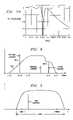
- FIG. 7Bshows the frequency response of the sound trap circuit of FIG. 7A ;
- FIG. 8shows the preferred frequency response in the second intermediate frequency filters (SIFFs) for an analog signal and the relationship between the picture, chroma and audio carriers;
- FIG. 9shows the preferred symmetrical frequency response in the second intermediate frequency filters (SIFFs) for a digital signal.
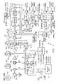
- FIG. 1is a high level block diagram which shows the components of the preferred embodiment of a dual mode tuner for coexisting digital and analog television signals.
- Signalsenter tuner 10 through low pass filter 100 .
- the cut-off frequency for filter 100is selected based upon the television system in which tuner 10 is implemented. In the United States, filter 100 would cut off frequencies above approximately 806 MHz. In a European television system the cut-off frequency could be higher depending upon the frequency band of the relevant television channels. In either system, the cutoff frequency of filter 100 is selected to suppress image frequencies.
- the disclosed tuner 10does not require a tracking filter on the front end. Instead filter 100 allows a broad band of frequencies to pass, subject only to the high frequency cutoff.
- Amplifier 101is capable of operating as a delayed automatic gain control (AGC) amplifier that is controlled by an AGC circuit.
- AGCdelayed automatic gain control
- the AGC circuit that controls amplifier 101will be discussed below in connection with item 60 and FIG. 6 .
- Amplifier 101provides delayed AGC to prevent the front end of tuner 10 from saturating. It is important that amplifier 101 is designed to have a very good noise figure, on the order of 5 or 6 dB, and very high intercept points to minimize distortion.
- Mixer 102accepts the output of amplifier 101 as one of its inputs.
- the other input to mixer 102is a local oscillator (LO 1 ) signal generated by phase locked loop 1 (PLL 1 ) 21 .
- LO 1local oscillator
- PLL 1phase locked loop 1
- Both mixer 102 and amplifier 101should have a very high dynamic range in order to handle the full television band.
- the television bandcan be up to 100 channels in the case of cable television and the signal strength of each channel can be as high as +15 dBmV.
- Mixer 102 and amplifier 101must have high third order and second order intercept points to minimize signal distortion.
- mixer 102is a Gilbert cell mixer that has been designed to have a good noise figure and a high intercept point.
- FIFF 103is intended to select down from the entire television band to just a few channels. Accordingly, it has to handle the 6 MHz television channel bandwidth plus some extra bandwidth to account for tuning and fine tuning in the LOs. In the preferred embodiment, FIFF 103 will nominally be 15 MHz wide. FIFF can either be an on-chip or an off-chip device. In the preferred embodiment FIFF 103 would be on-chip, however, design considerations may require that an off-chip filter be used for FIFF 103 .
- Mixer 104receives the output of FIFF 103 and mixes it with a second local oscillator (LO 2 ) signal generated by PLL 2 22 .
- PLL 2 22operates in conjunction with PPL 3 23 and PLL 4 24 .
- Mixer 104is an image reject mixer that works with FIFF 103 to suppress image frequencies from the output of mixer 104 .
- the signal coming out of filter 103is split into two signals, one at 0° phase and the other at 90° phase.
- the second LO signal from PLL 2 22is also composed of signals at 0° and 90°. These signals are applied to two mixers, the output of which is combined with the effect of rejecting the image frequency.
- the dynamic range of mixer 104does not have to be as broad as mixer 102 because FIFF 103 has the effect of filtering the signal down to just a few channels.
- the channel tuning in circuit 10is accomplished by the LO 1 and LO 2 signals generated by tuning circuit 20 .
- Coarse tuningis accomplished in mixer 102 by LO 1 .
- LO 1is generated by PLL 1 21 and has a step size of 5.25 MHz.
- Fine tuningis performed in mixer 104 by LO 2 .
- LO 2is generated using three phase locked loops PLL 2 - 4 22 - 24 and has a step size of 62.5 KHz. The operation of PLL 1 - 4 21 - 24 will be further discussed as part of FIG. 2 .
- SIFFa 106provides gain for the signal before it goes into second intermediate frequency filter “a” (SIFFa) 106 .
- SIFFa 106 and FIFF 103would be on-chip. Design considerations may suggest using off-chip filters for FIFF 103 , SIFFa 106 or SIFFb 109 . In an alternative embodiment, combinations of on-chip and off-chip filters may be used for FIFF 103 , SIFFa 106 or SIFFb 109 .
- SIFFa 106is chosen to have a pass band that is suitable for digital television signals. The pass band would be relatively flat over a 6 MHz frequency span as illustrated in FIG. 9 .
- Amplifier 107amplifies the signal following SIFFa 106 . If tuner circuit 10 is embodied so that filters 103 , 106 and 109 are off-chip devices, then they can typically be expected to have insertion loss of 3 to 15 dB. Amplifier 107 provides gain to compensate for the signal loss in SIFFa 106 , and may not be required.
- switch 108Following amplifier 107 is switch 108 which provides a selection between the second intermediate frequency filter “b” (SIFFb) 109 and attenuator 110 .
- Attenuator 110is chosen to match the insertion loss of filter 109 .
- the signal loss across switch 108will effectively remain the same and not vary with switch position.
- switch 108is selected to have isolation approximately 10 dB better than the analog audio suppression that is provided in SIFFb 109 .
- the analog audio suppressionis 20 dB, so switch 108 would be selected to have 30 to 35 dB isolation.
- SIFFb 109is designed to work in conjunction with SIFFa 106 to provide the band pass characteristics that are necessary for analog television signal processing.
- a typical analog signal pass bandis illustrated in FIG. 8 .
- switch 108selects SIFFb 109 into the signal path when an analog television signal is detected.
- the combined pass band through SIFFa 106 and SIFFb 109will be similar to that shown in FIG. 8 and will be optimized for processing the analog signal.
- switch 108selects attenuator 110 into the signal path.
- the resulting band pass of SIFFa 106 and attenuator 110will be similar to FIG. 9 and will be optimized for digital television signal processing.
- an analog band pass filter equivalent to the combination of SIFFa 106 and SIFFb 109could be placed in parallel with digital filter SIFFa 106 .
- This arrangementwould allow the analog and digital signal filters to be independent, but it would also require that switch 108 have an isolation on the order of 50 dB to prevent signals from leaking around the filters.
- Amplifier 111is a variable gain IF amplifier that provides the gain adjustment for the AGC circuit. Typically, amplifier 111 has a gain between 25 and 75 dB. The gain level is controlled by AGC control 60 .
- a key characteristic of amplifier 111is a noise figure on the order of 15 dB with high output intercept points on the order of +78 dB.
- buffer 112is a high end buffer output that provides a 44 MHz IF signal for external devices, such as a decoder, where the signal can be further processed off chip.
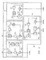
- COHO 40coherent oscillator circuit
- detector 50 awhich operates either as a video detector for analog television signals or as an in-phase down converter for digital television signals.
- COHO 40also provides a 90° phase signal to detector 50 b , which either operates as an audio down converter for analog television or as a quadrature detector for digital television.
- COHO 40is a phase lock loop reference that locks on the carrier for the received analog or digital television signal.
- the looprequires a bandwidth on the order of 25 KHz.
- the digital carrieris at a much lower level, a digital signal requires a bandwidth on the order of 1 KHz. Therefore, in the preferred embodiment, COHO 40 is designed to work on the digital bandwidth since it is within the analog bandwidth requirements.
- a narrow loop bandwidthcan be used in tuner circuit 10 because the close-in noise of LO 1 and LO 2 is very good.
- the loop bandwidth of the first local oscillatoris narrow which creates high noise close-in. That noise would have to be suppressed with a wide bandwidth COHO.
- the improved noise characteristics of LO 1 and LO 2allow the use of COHO 40 with a narrow loop bandwidth.
- COHO 40In addition to the signals provided to detectors 50 a and 50 b , COHO 40 also provides an output to frequency discriminator 113 .
- Frequency discriminator 113measures the actual frequency of the carrier signal that tuner circuit 10 is processing. This frequency information is provided to Inter Integrated Circuit interface, I 2 C 124 , which then adjusts PLL 1 - 4 21 - 24 as necessary to retune circuit 10 .
- I 2 Cis a well-known standard, defined by Philips Electronics N.V., but any digital interface will work. As shown in FIG. 8 , it is critical to place picture carrier 801 on the vestigial sideband slope 802 of the analog filter pass band. If picture carrier 801 is not properly positioned, the circuit will be retuned so that the carrier is at 45.75 MHz, plus or minus 35 KHz.
- the output of amplifier 111also directly drives video detector 50 a and audio detector 50 b .
- Video detector 50 adrives the in-phase digital channel, the analog video channel and automatic gain control (AGC) circuit 60 .
- the analog video channelincludes sound trap 70 which is a filter with a notch at the audio signal frequency of 4.5 MHz above the carrier. In the preferred embodiment, suppression at the trap frequency is on the order of 35 db. Also, sound trap 70 should have very little in-band distortion. It is desirable that sound trap 70 roll off above the audio signal trap frequency to suppress any out-of-band spurious signals or noise from video detector 50 a .
- the frequency response of the preferred embodiment of sound trap 70is shown in FIG. 7B .
- the in-phase channel for digital television signalsIn parallel with the analog video channel is the in-phase channel for digital television signals.
- the signalfirst passes through low pass filter 126 to suppress out of band noise and spurious signals.
- output buffer 114follows filter 126 and sets the levels for the digital I channel output signal.
- analog-to-digital (AID) converter 127could be placed between filter 126 and buffer 114 . If A/D converter 127 is used in the circuit, then the output from buffer 114 would be digital. In this embodiment, an off-chip A/D converter would not be needed.
- Sound trap 70drives noise clipping circuit 118 which clips off high frequency noise that could cause either high white levels or black levels.
- Noise clipping circuit 118is output buffer 115 .
- Buffer 115sets the signal level for the composite video output to approximately 1 volt peak-to-peak.
- Buffer 115also has a control input which can turn the output signal on and off.
- AGC circuit 60is the third path that is driven by detector 50 a .
- AGC 60measures the signal level output from detector 50 a and maintains a constant level at this point in circuit 10 .
- the signal from video detector 50 ais compared with a reference signal provided by I 2 C 124 .
- AGC 60controls the gain of circuit 10 by adjusting IF AGC amplifier 111 and delayed AGC amplifier 101 .
- AGC 60first adjusts IF AGC amplifier 111 to control the overall gain of tuner 10 . Once the gain gets to a specified minimum level, on the order of 25 dB, then AGC 60 adjusts delayed AGC amplifier 101 to attenuate the signal at the front end of tuner 10 .
- a delayed AGC signal from a decodercan also be used by AGC 60 to control the gain of tuner 10 .
- Such a delayed signalcould come from an off-chip decoder that is driven by the output of buffer 112 .
- the decoderWhen the decoder is active it could provide an AGC signal that would pass through AGC circuit 60 to directly control the gain of amplifier 101 and IF AGC amplifier 111 .
- Audio detector 50 buses the 90° signal from COHO 40 .
- the output of detector 50 bdrives the audio channel for analog television and the quadrature channel for digital television.
- the quadrature channelhas a low pass filter 128 of the same design as filter 126 in the in-phase digital channel. Filter 128 suppresses out-of-band noise and spurious signals and has a bandwidth on the order of 6 MHz.
- the signal from filter 128is passed through buffer 116 which has a control input to turn it on and off. Buffer 116 sets the output levels for the digital Q-channel.
- A/D converter 129may be placed between filter 128 and buffer 116 . A/D converter 129 would allow for direct digital output through buffer 116 without the need for an off-chip A/D converter for the digital signals.
- the signal on the analog audio channelfirst passes through chroma reject filter 119 .
- Filter 119is a high pass filter designed to suppresses any remaining luminance signal and to suppress the chroma carrier signal at approximately 3.58 MHz.
- the audio signal which is intended to be passed through filter 119is at 4.5 MHz after down converter 50 b .
- the output of filter 119is down converted in mixer 120 .
- the 4.5 MHz audio signalis mixed with a 5.25 MHz reference signal in mixer 120 to produce a 750 KHz output.
- the 750 KHz signalis then filtered by sound filter 121 .
- the bandwidth of sound filter 121is approximately 200 KHz.
- Sound filter 121is an on-chip circuit in the preferred embodiment. In an alternative embodiment, sound filtering could also be accomplished off-chip.
- the output of sound filter 121is provided to FM demodulator 122 .
- FM demodulator 122is a delay line type of demodulator in which the signal is split two ways. One path goes through a time delay and the other path goes into a multiplier circuit which produces an AM signal from the FM signal. In the preferred FM demodulator 122 , the time delay is a 90° phase shift at center frequency.
- the output of FM modulator 122drives audio output buffer 117 which sets the proper levels for the audio signal. Buffer 117 also has an on/off or mute control for the audio output.
- the reference signals used by tuner circuit 10are generated using, preferably, an off-chip 5.25 MHz crystal 1000 that is connected to oscillator circuit 123 .
- Circuit 123is on-chip and produces the basic 5.25 MHz reference signal for tuner 10 .
- the 5.25 MHz signaldrives reference frequency generator 125 which produces the other reference signals required by tuner 10 .
- the other reference signalsinclude a 2.625 MHz signal which is used in PLL 4 24 , a 262 KHz signal which is used for audio tuning and a 8.2 KHz signal which is used in the AGC circuit 60 .
- FIG. 2the four phase locked loops which produce the local oscillator signals for tuner 10 are shown.
- PLL 1 21provides the first local oscillator signal (LO 1 ) to mixer 102 .
- PLL 2 22 , PLL 3 23 and PLL 4 24operate to provide the second local oscillator signal (LO 2 ) to mixer 104 .
- Concurrently filed, co-pending application entitled “Interference Free Broadband Television Tuner”discusses the operation of tuning circuit 20 in greater detail and is incorporated by reference herein.
- PLL 1 21receives a 5.25 MHz reference signal at phase comparator 205 .
- the output of phase comparator 205feeds loop amplifier 202 which, in turn, provides the input for VCO 1 201 .
- One outputprovides the LO 1 signal to mixer 102 over line A.
- the other outputgoes into a divider network comprised of ⁇ 8/ ⁇ 9 circuit 203 and ⁇ N circuit 204 .
- Divider circuits 203 and 204divide the output of VCO 1 201 down to a signal having a frequency of 5.25 MHz. This divided-down signal is compared with the 5.25 MHz reference signal in phase comparator 205 to complete the phase locked loop.
- the 5.25 MHz reference signalcreates an output stepsize of 5.25 MHz which provides coarse tuning for tuner 10 .
- PLL 1 21has a bandwidth on the order of 500 KHz. A wide bandwidth is preferable to get good close-in phase noise characteristics.
- Fine tuningis accomplished by LO 2 which is produced by the operation of 3 phase lock loops PLL 2 22 , PLL 3 23 and PLL 4 24 .
- PLL 4 24has the same basic configuration as PLL 1 21 . It has reference signal of 2.625 MHz which is input to phase comparator 235 .
- the output of phase comparator 235drives loop amplifier 232 which in turn drives VCO 4 231 .
- the output of VCO 4 231has a 2.625 MHz stepsize and it is provided to two divider circuits.
- One output of VCO 4 231goes to a divider network comprised of ⁇ 6/ ⁇ 7 circuit 233 and ⁇ N circuit 234 .
- the effect of divider network 233 and 234is to divide the output signal of VCO 4 230 back down to 2.625 MHz. This signal is then compared with the 2.625 MHz reference signal in phase comparator 235 to complete the phase locked loop.
- the other output of VCO 4 231is provided to ⁇ 42 circuit 230 .
- the output of divider 230is a signal with a 62.5 KHz stepsize that serves as a reference signal for PLL 2 22 .
- the output of frequency divider 230varies between 5.25 MHz and 10.5 MHz in 62.5 KHz steps. This signal is provided to phase comparator 214 which in turn drives loop amplifier 213 . The output of loop amplifier 213 controls VCO 2 210 . VCO 2 210 provides the LO 2 signal for mixer 104 over line B. The other output from VCO 2 210 passes through buffer amplifier 211 and then drives image reject mixer 212 . Mixer 212 also receives an input from PLL 3 23 .
- phase detector 222drives loop amplifier 221 which in turn drives VCO 3 220 .
- the output of VCO 3 23is divided back down to 5.25 MHz by ⁇ N circuit 223 and then fed back into phase detector 222 to complete the loop.
- the output of VCO 3 23is in the range of 1 GHz which is close to the output frequency of VCO 2 210 . Therefore, buffer 211 is required to have good reverse isolation so that the signal from VCO 3 220 does not leak through to the output of VCO 2 210 and thereby get transmitted to mixer 104 as part of LO 2 .
- the loop bandwidths of PLL 2 22 , PLL 3 23 and PLL 4 24are all wide to provide good overall close-in phase noise.
- PLL 2 22 and PLL 3 23have bandwidths of approximately 300-500 KHz.
- the bandwidth of PLL 4 24is approximately 200-300 KHz. These bandwidths give phase noise of around 100 KHz which is satisfactory for digital television.
- the architecture of the frequency synthesis systemprovides for several benefits with respect to the overall operation of the tuner system. These benefits are in providing a lower distortion detection means, immunity to injection locking, a frequency synthesis system that allows for wide bandwidth PLLs while preserving a small step size, and providing for a choice of reference frequency that is out-of-band and that can be directly used to down-convert the audio portion of the desired channel.
- a wide loop bandwidth for LO 1 and LO 2is preferred because this yields good close-in phase noise characteristics for these two signals. This is important because it allows the COHO to have a narrow loop bandwidth, which yields a lower distortion video detector. For example, certain content within the video signal, such as the horizontal sync signal at approximately 15 KHz, would be partially tracked by a wide band COHO leading to distortion in the detection process. If the bandwidth of the COHO is less than 15 KHz, then the COHO would not partially track the horizontal sync signal leading to a near distortion free detection process. In the prior art, the oscillators used for conversion to IF typically do not have good close-in phase noise characteristics, requiring a COHO with wide loop bandwidth to track out this noise. It is thus typical in the prior art to employ wider bandwidth COHO's, which have the undesirable trait of partially tracking strong signals in the video signal, such as horizontal sync, leading to distortion in the detection process.
- the PLL reference frequencyis typically equal to the step size of the frequency synthesizer system. It is further typical of the prior art to employ a single loop frequency synthesizer to create the first LO in tuners. For example, if the step size of the system was 62.5 KHz, then the reference frequency to the single loop PLL would also be 62.5 KHz. It is highly desirable to suppress harmonics and spurs of the reference that are in band to a level below the noise floor of the VCO, requiring the loop bandwidth of the PLL to be less than the reference frequency. In the case where the reference is the step size, the loop bandwidth is rather narrow. Consequently, it is a clear advantage of the frequency synthesizer described herein to provide both a small step size as well as a wide bandwidth for LO 1 and LO 2 providing for enhanced immunity to spurs as well as providing for a narrow bandwidth COHO.
- a further advantage of the frequency synthesis systemis that it can use a reference that is above the baseband frequencies.
- An example of such a frequencyis 5.25 MHz. It should be noted that this 5.25 MHz reference is above the baseband signal of the system, thus avoiding in-band noise produced by the reference and its harmonics.
- a further advantage of this choice of referenceis that it can be used directly by the audio subsystem to down convert the frequency modulated audio signal to a lower frequency usable by the sound filter and FM demodulator in the audio subsystem. This eliminates the need for a PLL to create this frequency.
- FIG. 3shows automatic carrier detection (ACD) circuit 30 .
- ACDautomatic carrier detection
- the function of ACD circuit 30is to detect whether the incoming channel is an analog signal or a digital signal. If an analog signal is detected, ACD 30 also determines if it has a suppressed carrier or if the signal has been scrambled.
- ACD 30has two input lines C and D. The input on line C is from the output of SIFFa 106 . As discussed above and illustrated in FIG. 9 , SIFFa 106 has a band pass characteristic that is suitable for digital television. Line D input is from the output of SIFFb 109 . SIFFb 109 in combination with SIFFa 106 produces the band pass characteristics required for analog television, as shown in FIG. 8 .
- ACD 30operates by comparing the change in energy levels in the output of filters 106 and 109 .
- ACD 30uses amplitude detectors 301 and 302 to detect the power coming out of SIFFa and SIFFb. These levels are then compared in comparator 303 . The output of comparator 303 is then further compared with three different reference levels R 1 , R 2 and R 3 . In the preferred embodiment, ACD 30 would compare the ratio of the output of SIFFa 106 to the output of SIFFb 109 . If the received signal is an analog signal, then the ratio will be on the order of 6 dB. If the signal has a suppressed analog carrier, then the ratio will be on the order of 0 dB. For a digital signal the ratio will be on the order of 3 dB. The comparison in ACD 30 is provided by I 2 C 124 which adjusts switch 108 to select or deselect SIFFb 109 .
- the signal path of tuner 10is configured for analog television. That is, SIFFb 109 will be selected into the signal path by switch 108 . Following the comparison, if the signal is determined to be a digital television signal, SIFFb 109 will then be switched out of the signal path and attenuator 110 will be selected by switch 108 .
- Signal testingmay be initiated by a channel change. In that case, every time a new channel is selected, both SIFFa 106 and SIFFb 109 are switched into the circuit and ACD 30 compares signal levels on lines C and D. Following the test, I 2 C 124 either switches SIFFb 109 out or leaves it in the signal path depending on whether an analog or digital signal is detected.
- I 2 C 124can initiate signal testing in ACD 30 depending on any number of other factors. Signal testing could be initiated by a channel change, as discussed above, or by a change in the input source. For instance, if an operator switched the input from an antenna or cable line to a videotape recorder or laser disk player, then the test could be initiated even though the operator did not change the channel. ACD testing may be automatic or user-initiated. For example, a television system may provide a function on a remote control which allows the user to select the “test mode.”
- ACD 30is directly connected into the output of SIFFb 109 and SIFFb is always connected to amplifier 107 .
- This configurationwould not require switch 108 to select SIFFb 109 into the signal path in order to conduct the signal test.
- SIFFb 109could be configured to continuously receive the output of amplifier 107 over line 130 .
- Input D to ACD 30would be provided over line 131 directly from the output of SIFFb 109 rather than from the output of switch 108 . This would allow ACD 30 to continuously conduct the analog/digital signal determination test without regard to the position of switch 108 .
- Switch 108would only be changed to properly configure the signal path as required for the signal type detected.
- COHO 40shown in FIG. 4 , is comprised of a phase locked loop which provides reference signals to detectors 50 a and 50 b .
- the reference signal for detector 50 ais at 0° relative to the carrier signal for the analog or digital signal.
- the reference signal for down converter 50 bis at 90° with the phase of the carrier signal.
- the input to COHO 40is provided from amplifier 111 through converting circuit 41 .
- the signalpasses through current mode logic circuit 401 and divider 402 .
- VCO 43 of COHO 40runs at one quarter the frequency of the carrier signal.
- Circuit 41converts the input signal to current mode logic and then divides the signal frequency by 4 to match the frequency in the loop. Following divider 402 , the signal goes into phase detector 42 .
- phase detector 42passes through control circuit 44 and loop filter 423 and is then input to VCO 43 .
- VCO 43will normally operate at 11.4375 MHz.
- the output of VCO 43passes through frequency multiplier 420 which works in conjunction with VCO 43 to produce the in-phase/0° and quadrature/90° outputs at 45.75 MHz for detectors 50 a and 50 b .
- the output from multiplier 420also feeds back to phase detector 42 through current mode logic converter 421 and divider 422 to complete the phase locked loop circuit.
- Control logic 44is used in signal acquisition to ensure that COHO 40 searches in the correct direction and locks on the picture carrier for analog television signals, 801 of FIG. 8 , as opposed to locking on the neighboring audio signal 803 .
- Control 44does an upsweep search looking for the picture carrier 801 to avoid locking on to the higher frequency audio carrier 803 .
- Thisis important for situations in which the carrier is off-frequency. For example, in a cable television analog signal, the carrier frequency can be off by up to 2 MHz. Accordingly, COHO 40 needs control 44 to ensure that the loop locks onto the proper frequency. It is likely that digital television signals will also vary up to 2 MHz from the expected frequency in some situations. Therefore, control 44 is used for both analog and digital signals.
- Circuit 413compares the actual output frequency of VCO 43 with the expected frequency of 11.4375 MHz. Circuit 413 generates an error signal which is provided to control logic gates 408 - 410 . The output of gates 408 - 410 goes into up-down counter 411 . Digital-to-analog converter 412 converts the output of counter 411 to an analog error signal which is added into the signal path by adder 404 . The output of adder 404 provides an offset control signal for VCO 43 .
- Sweep circuit 416forces control 44 to search from lower frequencies to higher frequencies to avoid locking on audio signal 803 instead of picture carrier 801 .
- the output of sweep circuit 416is provided to adder 403 which adds an offset to the output of phase detector 42 to force this sweep in the right direction.
- This low-to-high acquisitioncould also be implemented by setting the bias for VCO 43 to a low level, thereby forcing the output of VCO 43 to a low frequency.
- the error signal from phase detector 42would then pull the bias for VCO 43 up in frequency in which case it will sweep in the correct direction.
- Detector 415 and latch 414function as a lock detection circuit.
- the signal from phase detector 42is compared to a reference signal and if the signal is inside the reference then it is locked, otherwise it is not locked.
- the signal from latch 414is provided to logic gates 406 and 407 along with the output of comparator 405 .
- the output of gates 406 and 407serves as the other input for logic gates 408 - 410 . I have found that dividers 402 and 422 may not be necessary.
- FIG. 5show the components of a Gilbert cell mixer such as that used for detectors 50 a and 50 b .
- the inputs to the Gilbert cellare a local oscillator (LO) signal and a RF signal.
- the LOis an in-phase signal from COHO 40 .
- Audio/quadrature detector 50 breceives a 90° phase signal from COHO 40 as the LO.
- the signals in the preferred embodimentare balanced but for clarity they are shown as single inputs to buffers 51 and 52 .
- Mixer 50itself is totally balanced and receives balanced inputs.
- the output of mixer 50is also balanced although it is shown as a single ended output through buffer 53 for simplification of the drawings.
- Mixer 50is a common Gilbert cell with a top section of transistors, 501 , 502 , 503 , and 504 which are switched on and off by the LO signal.
- Transistors 506 and 505are modulated with the RF signal input.
- the RF signalis provided by amplifier 111 .
- Resistors 507 and 508are used to provide or improve circuit linearity.
- Current source 509provides the current to drive the system and may be implemented by any number of current circuits that are well known in the art.
- Resistors 510 and 511provide biasing for the collectors of transistors 501 - 504 .
- AGC Circuit 60is shown in further detail in FIG. 6 .
- AGC 60operates to control the gain of tuner 10 by adjusting the gain of amplifiers 101 and 111 .
- IF AGC amplifier 111is used to lower the overall receiver gain. Once amplifier 111 reaches a minimum gain level on the order of 25 dB, then delayed AGC amplifier 101 is adjusted to attenuate the signal at the front end of tuner 10 .
- AGC 60receives an input from video detector 50 a .
- the input signalgoes into peak detect and dump circuit 61 .
- peak detect and dump circuit 61searches for the peak signal level and holds that until it gets sampled on a command from selector 63 .
- Selector 63can select between a sync clamp pulse or a programmable sample strobe.
- a sync clamp circuit(not shown) provides the sync clamp pulse for analog television signals. Use of the sync clamp pulse phase locks the operation of AGC 60 to the horizontal sync of the analog television signal.
- the sync pulseis the largest signal in the analog television signal and so it provides an easily useable synchronous means of sampling signals for AGC 60 .
- the sync pulsedoes not apply for digital television or for a scrambled analog television signal in which the picture carrier reference signal is typically suppressed.
- a programmable sample strobeis used for those cases where the sync pulse is not available or if the sync clamp circuit is not used.
- Peak detect and dump 61works with both analog and digital television signals and provides an output to loop amplifier 62 .
- Loop amplifier 62receives an AGC reference signal that is provided by I 2 C 124 .
- the output of amplifier 62goes into sample and hold circuit 65 .
- Sample and hold 65also receives a sample strobe from selector 63 . As a result, the output of sample and hold 65 is also strobed. The output is fed back and added to the input by integrator 64 .
- the output of sample and hold 65goes to linearizer circuits 66 and 67 , which linearize the control current for amplifiers 111 and 101 .
- the AGC referencecan bypass loop amplifier 62 and sample and hold 65 and go directly into linearizers 66 and 67 . This would allow for manual control of the receiver gain for test purposes.
- the programmable sample strobe from selector 63is made programmable to allow for variable AGC loop bandwidths. By changing divide ratios the loop bandwidth can be varied and optimized for various television signals.
- AGC 60can also receive a delayed AGC input from an off-chip decoder.
- tuner 10When tuner 10 is used with a decoder that receives an IF signal from buffer 112 , the decoder can provide an input back into AGC 60 to directly control the end gain at AGC amplifier 101 and IF amplifier 111 .
- Sound trap 70can either be an on-chip or off-chip device.
- FIG. 7Ashows an on-chip design for sound trap 70 that is implemented with several stages of circuits having relatively low Q poles and zeros.
- the intent of sound trap 70is to provide a null at the sound carrier frequency of 4.5 MHz as shown in FIG. 7B . This prevents the sound carrier signal from passing to the output of the video port at buffer 115 .
- Sound trap 70is optimally designed to have a minimal amount of ripple in-band and in the notch at 4.5 MHz. It should also have a fall off in the out-of-band response to suppress noise and spurious signals.
- Circuit 7Ahas a series of bi-quad circuits which are used to implement the poles and zeros necessary to obtain the desired frequency response.
- Circuits 71 - 75each provide two stages of filtering for a total of ten filter stages. The filters are followed by buffer stage 76 .
- Circuit 77provides bias control for filter stages 71 - 75 and buffer 76 .
- a digital television standard in the United Statesmay vary from the digital standard used in Japan, European or elsewhere.
- the varying analog television signal standardsillustrate the potential for different standards in different countries.
- NSCNational Television Systems Committee
- PALPhase Alternate Line
- tunerwhich allows for more than two signal formats to be processed.
- the disclosed tunercould also be embodied to provide multiple output signals which correspond to more than just simple analog and digital formats.
- the tuner described hereincould be used in a known (or unknown) single system format by presetting certain values, either in response to a separately received central signal, or manually, or a decoded control signal. In such a context it could be advantageous to use the range of input filter 100 , either on its high or low side, or both. This variable control can be manual, or under control of an applied signal on a dynamic basis.
- the disclosed tunerwould be manufactured on a single integrated circuit substrate.
- design considerationsmay require that certain elements be embodied as discrete devices (herein called off-chip) instead of incorporating the elements into an integrated substrate.
- the IF filters, analog-to-digital converter, sound trap filter or input filtermay be incorporated as off-chip elements as necessary while still achieving the desired dual mode tuning circuit.
- a single board, or chipcould contain multiple “off-chip” elements and one or more integrated circuits. In such a context, the designation “off-chip” simply implies that some of the elements are all not within a common substrate.
- Another alternative designwould simplify FIFF 103 , thereby allowing the entire range of channels in the RF signal to be converted to the second IF signal.
- the conversion circuitcould be constructed entirely on an integrated substrate and filtering of unwanted channels could be accomplished after the RF signal has been converted to a second IF signal.
Landscapes
- Engineering & Computer Science (AREA)
- Power Engineering (AREA)
- Multimedia (AREA)
- Signal Processing (AREA)
- Superheterodyne Receivers (AREA)
- Noise Elimination (AREA)
Abstract
Description
Claims (34)
Priority Applications (1)
| Application Number | Priority Date | Filing Date | Title |
|---|---|---|---|
| US10/459,125US7707617B2 (en) | 1997-08-01 | 2003-06-11 | Dual mode tuner for co-existing digital and analog television signals |
Applications Claiming Priority (2)
| Application Number | Priority Date | Filing Date | Title |
|---|---|---|---|
| US08/904,693US6725463B1 (en) | 1997-08-01 | 1997-08-01 | Dual mode tuner for co-existing digital and analog television signals |
| US10/459,125US7707617B2 (en) | 1997-08-01 | 2003-06-11 | Dual mode tuner for co-existing digital and analog television signals |
Related Parent Applications (1)
| Application Number | Title | Priority Date | Filing Date |
|---|---|---|---|
| US08/904,693DivisionUS6725463B1 (en) | 1997-08-01 | 1997-08-01 | Dual mode tuner for co-existing digital and analog television signals |
Publications (2)
| Publication Number | Publication Date |
|---|---|
| US20040004674A1 US20040004674A1 (en) | 2004-01-08 |
| US7707617B2true US7707617B2 (en) | 2010-04-27 |
Family
ID=30001175
Family Applications (2)
| Application Number | Title | Priority Date | Filing Date |
|---|---|---|---|
| US08/904,693Expired - LifetimeUS6725463B1 (en) | 1997-08-01 | 1997-08-01 | Dual mode tuner for co-existing digital and analog television signals |
| US10/459,125Expired - LifetimeUS7707617B2 (en) | 1997-08-01 | 2003-06-11 | Dual mode tuner for co-existing digital and analog television signals |
Family Applications Before (1)
| Application Number | Title | Priority Date | Filing Date |
|---|---|---|---|
| US08/904,693Expired - LifetimeUS6725463B1 (en) | 1997-08-01 | 1997-08-01 | Dual mode tuner for co-existing digital and analog television signals |
Country Status (1)
| Country | Link |
|---|---|
| US (2) | US6725463B1 (en) |
Cited By (16)
| Publication number | Priority date | Publication date | Assignee | Title |
|---|---|---|---|---|
| US20090251181A1 (en)* | 2008-04-08 | 2009-10-08 | Bae Seung Jun | Method and apparatus for tuning phase of clock signal |
| US20100045874A1 (en)* | 2005-01-28 | 2010-02-25 | Nxp B.V. | Intermediate frequency processing device for processing both analogue and digital television intermediate frequency signals |
| US9021538B2 (en) | 1998-07-14 | 2015-04-28 | Rovi Guides, Inc. | Client-server based interactive guide with server recording |
| US9036741B2 (en) | 2012-12-28 | 2015-05-19 | Motorola Solutions, Inc. | Systems, methods, and devices for frequency-selective AGC |
| US9055322B2 (en) | 2001-02-21 | 2015-06-09 | Rovi Guides, Inc. | Systems and methods for interactive program guides with personal video recording features |
| US9071872B2 (en) | 2003-01-30 | 2015-06-30 | Rovi Guides, Inc. | Interactive television systems with digital video recording and adjustable reminders |
| US9075861B2 (en) | 2006-03-06 | 2015-07-07 | Veveo, Inc. | Methods and systems for segmenting relative user preferences into fine-grain and coarse-grain collections |
| US9166714B2 (en) | 2009-09-11 | 2015-10-20 | Veveo, Inc. | Method of and system for presenting enriched video viewing analytics |
| US9191722B2 (en) | 1997-07-21 | 2015-11-17 | Rovi Guides, Inc. | System and method for modifying advertisement responsive to EPG information |
| US9294799B2 (en) | 2000-10-11 | 2016-03-22 | Rovi Guides, Inc. | Systems and methods for providing storage of data on servers in an on-demand media delivery system |
| US9319735B2 (en) | 1995-06-07 | 2016-04-19 | Rovi Guides, Inc. | Electronic television program guide schedule system and method with data feed access |
| US9326025B2 (en) | 2007-03-09 | 2016-04-26 | Rovi Technologies Corporation | Media content search results ranked by popularity |
| US9426509B2 (en) | 1998-08-21 | 2016-08-23 | Rovi Guides, Inc. | Client-server electronic program guide |
| US9736524B2 (en) | 2011-01-06 | 2017-08-15 | Veveo, Inc. | Methods of and systems for content search based on environment sampling |
| US9749693B2 (en) | 2006-03-24 | 2017-08-29 | Rovi Guides, Inc. | Interactive media guidance application with intelligent navigation and display features |
| US10063934B2 (en) | 2008-11-25 | 2018-08-28 | Rovi Technologies Corporation | Reducing unicast session duration with restart TV |
Families Citing this family (109)
| Publication number | Priority date | Publication date | Assignee | Title |
|---|---|---|---|---|
| US6177964B1 (en)* | 1997-08-01 | 2001-01-23 | Microtune, Inc. | Broadband integrated television tuner |
| KR100269159B1 (en)* | 1998-09-05 | 2000-10-16 | 윤종용 | Tuner Circuit Design Method |
| US6995808B2 (en)* | 2002-01-24 | 2006-02-07 | Sige Semiconductor Inc. | Television tuner |
| EP1128546A1 (en)* | 2000-02-28 | 2001-08-29 | Deutsche Thomson-Brandt Gmbh | Upconverter mixer circuit |
| US6933986B2 (en)* | 2000-04-07 | 2005-08-23 | Harris Corporation | Sharply tuned bandpass filter |
| EP1277336A2 (en)* | 2000-04-07 | 2003-01-22 | Harris Corporation | Sharply tuned bandpass filter |
| JP2001339320A (en)* | 2000-05-25 | 2001-12-07 | Sony Corp | Interference wave elimination circuit and digital television receiver |
| US6995806B1 (en)* | 2000-08-04 | 2006-02-07 | Scientific-Atlanta, Inc. | Amplifier with a universal automatic gain control circuit |
| JP2002185880A (en)* | 2000-12-14 | 2002-06-28 | Sony Corp | Information processing unit and method, receiver and method, and recording medium |
| US20040201779A1 (en)* | 2001-02-02 | 2004-10-14 | Spilker James J. | Symbol clock recovery for the ATSC digital television signal |
| JP3850225B2 (en)* | 2001-03-27 | 2006-11-29 | シャープ株式会社 | Tuner for cable modem |
| JP3882524B2 (en)* | 2001-04-06 | 2007-02-21 | 松下電器産業株式会社 | Broadband tuner |
| GB0117591D0 (en)* | 2001-07-18 | 2001-09-12 | Zarlink Semiconductor Ltd | Television tuner |
| JP2003037516A (en)* | 2001-07-23 | 2003-02-07 | Funai Electric Co Ltd | Broadcast receiver having automatic gain control function |
| CN1572107A (en)* | 2001-10-16 | 2005-01-26 | Rf信息公司 | Methods and apparatus for implementing a receiver on a monolithic integrated circuit |
| JP2003152561A (en)* | 2001-11-08 | 2003-05-23 | Alps Electric Co Ltd | Frequency conversion circuit |
| JP2003152668A (en)* | 2001-11-12 | 2003-05-23 | Kobe Steel Ltd | Frequency converting device |
| DE10163798A1 (en)* | 2001-12-22 | 2003-07-03 | Philips Intellectual Property | TV signal receiver with universal output for various surface wave filters |
| US7020230B2 (en)* | 2001-12-28 | 2006-03-28 | Tropian, Inc. | Frequency synthesizer for dual mode receiver |
| JP3906792B2 (en)* | 2002-01-22 | 2007-04-18 | 松下電器産業株式会社 | High frequency signal receiving apparatus and manufacturing method thereof |
| US7199844B2 (en)* | 2002-05-28 | 2007-04-03 | Rfstream Corporation | Quadratic nyquist slope filter |
| US7116961B2 (en)* | 2002-05-29 | 2006-10-03 | Rfstream Corporation | Image rejection quadratic filter |
| CN100433542C (en)* | 2002-06-05 | 2008-11-12 | Rf信息公司 | Quadratic video demodulation with baseband nyquist filter |
| US6882245B2 (en)* | 2002-06-05 | 2005-04-19 | Rf Stream Corporation | Frequency discrete LC filter bank |
| US7414676B2 (en)* | 2002-07-31 | 2008-08-19 | Conexant Systems, Inc. | Integrated programmable tuner |
| JP3092726U (en)* | 2002-09-11 | 2003-03-28 | アルプス電気株式会社 | Television tuner |
| JP2004159056A (en)* | 2002-11-06 | 2004-06-03 | Renesas Technology Corp | Signal generation circuit |
| US7035614B2 (en)* | 2002-12-13 | 2006-04-25 | Microtune (Texas), L.P. | System and method for discovering frequency related spurs in a multi-conversion tuner |
| US20040125239A1 (en)* | 2002-12-26 | 2004-07-01 | David Rahn | Television tuner supporting channel hopping |
| US7120413B2 (en) | 2003-06-22 | 2006-10-10 | Realtek Semiconductor Corp. | Television tuner and method of processing a received RF signal |
| US7262815B2 (en)* | 2003-06-22 | 2007-08-28 | Realtek Semiconductor Corp. | Harmonic mixer based television tuner and method of processing a received RF signal |
| US7180553B2 (en)* | 2003-06-22 | 2007-02-20 | Realtek Semiconductor Corp. | Dual mode television tuner capable of processing both digital and satellite television signals and method thereof |
| US6940365B2 (en) | 2003-07-18 | 2005-09-06 | Rfstream Corporation | Methods and apparatus for an improved discrete LC filter |
| US7310505B2 (en)* | 2003-09-09 | 2007-12-18 | Zenith Electronics Corporation | Attenuation control for tuners |
| JP4397205B2 (en)* | 2003-10-02 | 2010-01-13 | 三洋電機株式会社 | Broadcast receiver |
| KR20050034966A (en)* | 2003-10-10 | 2005-04-15 | 삼성전기주식회사 | Receiver for down-conversion of dual band from dmb/dab |
| US20050079840A1 (en)* | 2003-10-11 | 2005-04-14 | Visteon Global Technologies, Inc. | Method for controlling the selectivity of a tuner in a variable bandwidth system |
| US7202916B2 (en)* | 2003-12-15 | 2007-04-10 | Realtek Semiconductor Corp. | Television tuner and method of processing a received RF signal |
| US7355612B2 (en)* | 2003-12-31 | 2008-04-08 | Hewlett-Packard Development Company, L.P. | Displaying spatially offset sub-frames with a display device having a set of defective display pixels |
| US7477325B2 (en)* | 2004-03-29 | 2009-01-13 | Ati Technologies, Inc. | Audio/video separator |
| US7091982B2 (en)* | 2004-05-14 | 2006-08-15 | Nvidia Corporation | Low power programmable processor |
| US7389006B2 (en)* | 2004-05-14 | 2008-06-17 | Nvidia Corporation | Auto software configurable register address space for low power programmable processor |
| KR101101689B1 (en)* | 2004-05-19 | 2011-12-30 | 톰슨 라이센싱 | Filter configuration for multiple broadcast standard signal receivers |
| US7929649B2 (en)* | 2004-06-30 | 2011-04-19 | Stmicroelectronics, Inc. | Analog/digital carrier differentiation in digital cable receivers |
| DE102004034274A1 (en)* | 2004-07-15 | 2006-02-09 | Infineon Technologies Ag | Receiver arrangement, in particular for the digital television distribution service and use thereof |
| US20060028587A1 (en)* | 2004-08-05 | 2006-02-09 | Peng Juen T | TV tuner |
| US7551229B2 (en)* | 2004-08-13 | 2009-06-23 | Sony Corporation | Automatic channel selection method and apparatus in unstable digital channel environments |
| US8160526B2 (en) | 2004-08-13 | 2012-04-17 | Thomson Licensing | Filter configuration for a receiver of multiple broadcast standard signals |
| EP1627672B1 (en)* | 2004-08-17 | 2011-07-27 | Dialog Semiconductor GmbH | Control of illumination of a mobile phone by using audio signals |
| EP1631079A1 (en)* | 2004-08-31 | 2006-03-01 | Harman Becker Automotive Systems GmbH | A mobile television receiver and method for automatically identifying the transmission standard of broadcast television signals |
| US7394500B2 (en)* | 2004-09-13 | 2008-07-01 | Ati Technologies Inc. | World wide analog television signal receiver |
| US7904024B2 (en)* | 2004-09-28 | 2011-03-08 | Zoran Corporation | System and method of eliminating or minimizing Lo-Related interference from tuners |
| US7432981B1 (en)* | 2004-12-13 | 2008-10-07 | Nvidia Corporation | Apparatus, system, and method for processing digital audio/video signals |
| KR100620964B1 (en)* | 2005-01-07 | 2006-09-14 | 삼성전자주식회사 | Image display device capable of analog / digital tuning by DV tuner and its analog / digital tuning method |
| US7369835B2 (en)* | 2005-03-10 | 2008-05-06 | Xceive Corporation | Image rejection mixer providing precision image rejection |
| US7446631B2 (en) | 2005-03-11 | 2008-11-04 | Rf Stream Corporation | Radio frequency inductive-capacitive filter circuit topology |
| JP2008533839A (en)* | 2005-03-11 | 2008-08-21 | 株式会社RfStream | Broadband tuning circuit |
| US7358795B2 (en)* | 2005-03-11 | 2008-04-15 | Rfstream Corporation | MOSFET temperature compensation current source |
| US8132214B2 (en)* | 2008-04-03 | 2012-03-06 | Echostar Technologies L.L.C. | Low noise block converter feedhorn |
| US20070132889A1 (en)* | 2005-11-28 | 2007-06-14 | Jianping Pan | Integrated digital television tuner |
| US7830456B1 (en)* | 2006-06-02 | 2010-11-09 | Anadigics, Inc | System and method for frequency multiplexing in double-conversion receivers |
| US20080143885A1 (en)* | 2006-12-14 | 2008-06-19 | Analog Devices, Inc. | Television upconverter structures |
| US8902365B2 (en)* | 2007-03-14 | 2014-12-02 | Lance Greggain | Interference avoidance in a television receiver |
| US8330873B2 (en)* | 2007-03-14 | 2012-12-11 | Larry Silver | Signal demodulator with overmodulation protection |
| TW200919948A (en)* | 2007-10-18 | 2009-05-01 | Rafael Microelectronics Inc | Tuner with power management means |
| KR101564122B1 (en) | 2008-01-30 | 2015-10-28 | 톰슨 라이센싱 | Tuner comprising an if filter with a controllable damping stage and receiver comprising a respective tuner |
| US8169546B2 (en)* | 2008-02-19 | 2012-05-01 | Newport Media, Inc. | Technique for tuner automatic gain control circuit for mobile television applications |
| US9363469B2 (en) | 2008-07-17 | 2016-06-07 | Ppc Broadband, Inc. | Passive-active terminal adapter and method having automatic return loss control |
| JPWO2010018780A1 (en)* | 2008-08-11 | 2012-01-26 | ソニー株式会社 | Receiving device, receiving method and program |
| TW201015996A (en)* | 2008-10-07 | 2010-04-16 | Sunplus Technology Co Ltd | Multi-standard integrated television receiver |
| US9647851B2 (en) | 2008-10-13 | 2017-05-09 | Ppc Broadband, Inc. | Ingress noise inhibiting network interface device and method for cable television networks |
| US8516537B2 (en)* | 2009-10-09 | 2013-08-20 | Ppc Broadband, Inc. | Downstream bandwidth conditioning device |
| US20110085586A1 (en)* | 2009-10-09 | 2011-04-14 | John Mezzalingua Associates, Inc. | Total bandwidth conditioning device |
| US8464301B2 (en)* | 2008-10-16 | 2013-06-11 | Ppc Broadband, Inc. | Upstream bandwidth conditioning device between CATV distribution system and CATV user |
| US8832767B2 (en)* | 2008-10-16 | 2014-09-09 | Ppc Broadband, Inc. | Dynamically configurable frequency band selection device between CATV distribution system and CATV user |
| US8001579B2 (en)* | 2008-10-16 | 2011-08-16 | John Mezzalingua Associates, Inc. | Downstream output level and/or output level tilt compensation device between CATV distribution system and CATV user |
| US8385219B2 (en)* | 2009-10-09 | 2013-02-26 | John Mezzalingua Associates, Inc. | Upstream bandwidth level measurement device |
| US8213457B2 (en)* | 2009-10-09 | 2012-07-03 | John Mezzalingua Associates, Inc. | Upstream bandwidth conditioning device |
| KR20100042784A (en)* | 2008-10-17 | 2010-04-27 | 삼성전자주식회사 | Apparatus and method for receiving broadcasting of two mode using one tuner in set top box |
| US11910052B2 (en) | 2008-10-21 | 2024-02-20 | Ppc Broadband, Inc. | Entry device for communicating external network signals and in-home network signals |
| US8510782B2 (en) | 2008-10-21 | 2013-08-13 | Ppc Broadband, Inc. | CATV entry adapter and method for preventing interference with eMTA equipment from MoCA Signals |
| US8181211B2 (en)* | 2009-03-30 | 2012-05-15 | John Mezzalingua Associates, Inc. | Total bandwidth conditioning device |
| US8212923B2 (en)* | 2010-04-13 | 2012-07-03 | Newport Media, Inc. | SECAM line identification and PAL switch |
| US8479247B2 (en) | 2010-04-14 | 2013-07-02 | Ppc Broadband, Inc. | Upstream bandwidth conditioning device |
| US9030536B2 (en) | 2010-06-04 | 2015-05-12 | At&T Intellectual Property I, Lp | Apparatus and method for presenting media content |
| US8640182B2 (en) | 2010-06-30 | 2014-01-28 | At&T Intellectual Property I, L.P. | Method for detecting a viewing apparatus |
| US8593574B2 (en)* | 2010-06-30 | 2013-11-26 | At&T Intellectual Property I, L.P. | Apparatus and method for providing dimensional media content based on detected display capability |
| US9787974B2 (en) | 2010-06-30 | 2017-10-10 | At&T Intellectual Property I, L.P. | Method and apparatus for delivering media content |
| US8918831B2 (en) | 2010-07-06 | 2014-12-23 | At&T Intellectual Property I, Lp | Method and apparatus for managing a presentation of media content |
| US9049426B2 (en) | 2010-07-07 | 2015-06-02 | At&T Intellectual Property I, Lp | Apparatus and method for distributing three dimensional media content |
| US9232274B2 (en) | 2010-07-20 | 2016-01-05 | At&T Intellectual Property I, L.P. | Apparatus for adapting a presentation of media content to a requesting device |
| US9032470B2 (en) | 2010-07-20 | 2015-05-12 | At&T Intellectual Property I, Lp | Apparatus for adapting a presentation of media content according to a position of a viewing apparatus |
| US9560406B2 (en) | 2010-07-20 | 2017-01-31 | At&T Intellectual Property I, L.P. | Method and apparatus for adapting a presentation of media content |
| KR101052034B1 (en)* | 2010-07-23 | 2011-07-26 | 삼성탈레스 주식회사 | Multifunction receiver of electronic warfare system |
| US8994716B2 (en) | 2010-08-02 | 2015-03-31 | At&T Intellectual Property I, Lp | Apparatus and method for providing media content |
| US8438502B2 (en) | 2010-08-25 | 2013-05-07 | At&T Intellectual Property I, L.P. | Apparatus for controlling three-dimensional images |
| US8561125B2 (en) | 2010-08-30 | 2013-10-15 | Ppc Broadband, Inc. | Home network frequency conditioning device and method |
| US8947511B2 (en) | 2010-10-01 | 2015-02-03 | At&T Intellectual Property I, L.P. | Apparatus and method for presenting three-dimensional media content |
| WO2012088350A2 (en) | 2010-12-21 | 2012-06-28 | John Mezzalingua Associates, Inc. | Method and apparatus for reducing isolation in a home network |
| US9036091B2 (en)* | 2011-01-06 | 2015-05-19 | Silicon Laboratories Inc. | Receiver and method of receiving analog and digital television signals |
| US9602766B2 (en) | 2011-06-24 | 2017-03-21 | At&T Intellectual Property I, L.P. | Apparatus and method for presenting three dimensional objects with telepresence |
| US9030522B2 (en) | 2011-06-24 | 2015-05-12 | At&T Intellectual Property I, Lp | Apparatus and method for providing media content |
| US8947497B2 (en) | 2011-06-24 | 2015-02-03 | At&T Intellectual Property I, Lp | Apparatus and method for managing telepresence sessions |
| US9445046B2 (en) | 2011-06-24 | 2016-09-13 | At&T Intellectual Property I, L.P. | Apparatus and method for presenting media content with telepresence |
| US8587635B2 (en) | 2011-07-15 | 2013-11-19 | At&T Intellectual Property I, L.P. | Apparatus and method for providing media services with telepresence |
| US20130249821A1 (en)* | 2011-09-27 | 2013-09-26 | The Board of Trustees of the Leland Stanford, Junior, University | Method and System for Virtual Keyboard |
| US10317535B2 (en) | 2016-03-31 | 2019-06-11 | Samsung Electronics Co., Ltd | Method and apparatus for second order intercept point (IP2) calibration |
| TWM583659U (en)* | 2019-02-20 | 2019-09-11 | 訊鼎電子股份有限公司 | Cable television system with printed-circuit-board-layout components |
| CN115001489B (en)* | 2022-05-27 | 2025-03-25 | 电子科技大学 | A low-noise millimeter-wave fractional frequency synthesizer phase-locked loop structure |
Citations (28)
| Publication number | Priority date | Publication date | Assignee | Title |
|---|---|---|---|---|
| US4030035A (en)* | 1974-10-02 | 1977-06-14 | Hitachi, Ltd. | Circuit for preventing output clipping of R.F. stage in radio receiver |
| US4385402A (en) | 1980-04-16 | 1983-05-24 | Redifon Telecommunications Limited | Switchable filter circuits |
| US4581643A (en) | 1983-07-25 | 1986-04-08 | Rca Corporation | Double conversion television tuner with frequency response control provisions |
| US4726072A (en) | 1983-07-28 | 1988-02-16 | Matsushita Electric Industrial Co., Ltd. | Double converter tuner |
| US4742566A (en) | 1985-03-11 | 1988-05-03 | U.S. Philips Corporation | AM receiver |
| US4979230A (en) | 1989-12-04 | 1990-12-18 | General Instrument Corporation | Up-conversion homodyne receiver for cable television converter with frequency offset to avoid adjacent channel interference |
| US5038404A (en) | 1989-09-01 | 1991-08-06 | General Instrument Corp. | Low phase noise agile up converter |
| US5060297A (en) | 1988-04-04 | 1991-10-22 | Ma John Y | TVRO receiver system with tracking filter for rejection of image frequencies |
| US5200826A (en) | 1990-06-21 | 1993-04-06 | Samsung Electronics Co., Ltd. | TV signal receiving double conversion television tuner system having automatic gain control provisions |
| US5262957A (en)* | 1990-11-09 | 1993-11-16 | Global Communications, Inc. | Inexpensive portable RF spectrum analyzer with calibration features |
| US5311318A (en) | 1992-08-17 | 1994-05-10 | Zenith Electronics Corporation | Double conversion digital tuning system using separate digital numbers for controlling the local oscillators |
| US5361099A (en) | 1992-10-29 | 1994-11-01 | Goldstar Co., Ltd. | NTSC/HDTV community receiving system |
| US5390346A (en) | 1994-01-21 | 1995-02-14 | General Instrument Corporation Of Delaware | Small frequency step up or down converters using large frequency step synthesizers |
| US5428836A (en) | 1992-01-21 | 1995-06-27 | Motorola Inc. | Radio receiver for forming a baseband signal of time-varying frequencies |
| US5557337A (en) | 1994-02-18 | 1996-09-17 | Hitachi America, Ltd. | Automatic television signal detector to differentiate NTSC signals from HDJV/AJV signals |
| US5563545A (en) | 1992-03-03 | 1996-10-08 | Anadigics, Inc. | Low cost monolithic GaAs upconverter chip |
| US5572264A (en) | 1994-02-14 | 1996-11-05 | Hitachi, Ltd. | High definition TV signal receiver |
| US5638112A (en) | 1995-08-07 | 1997-06-10 | Zenith Electronics Corp. | Hybrid analog/digital STB |
| US5715012A (en) | 1996-03-13 | 1998-02-03 | Samsung Electronics Co., Ltd. | Radio receivers for receiving both VSB and QAM digital HDTV signals |
| US5737035A (en)* | 1995-04-21 | 1998-04-07 | Microtune, Inc. | Highly integrated television tuner on a single microcircuit |
| US5847612A (en) | 1997-08-01 | 1998-12-08 | Microtune, Inc. | Interference-free broadband television tuner |
| US5950112A (en) | 1995-12-04 | 1999-09-07 | Sharp Kabushiki Kaisha | Satelite broadcast tuner capable of processing both QPSK modulation signal and FM signal |
| US6014178A (en) | 1995-09-29 | 2000-01-11 | Samsung Electronics Co., Ltd. | Receiver having analog and digital video modes and receiving method thereof |
| US6094236A (en)* | 1996-04-26 | 2000-07-25 | Kabushiki Kaisha Toshiba | Tuner circuit |
| US6094564A (en) | 1996-04-08 | 2000-07-25 | Matsushita Electric Industrial Co., Ltd. | Mobile communication apparatus operable in different formats and pairing I-F band pass filter type with I-F amplifier characteristics |
| US6163684A (en) | 1997-08-01 | 2000-12-19 | Microtune, Inc. | Broadband frequency synthesizer |
| US6177964B1 (en) | 1997-08-01 | 2001-01-23 | Microtune, Inc. | Broadband integrated television tuner |
| US6377315B1 (en)* | 1998-11-12 | 2002-04-23 | Broadcom Corporation | System and method for providing a low power receiver design |
- 1997
- 1997-08-01USUS08/904,693patent/US6725463B1/ennot_activeExpired - Lifetime
- 2003
- 2003-06-11USUS10/459,125patent/US7707617B2/ennot_activeExpired - Lifetime
Patent Citations (29)
| Publication number | Priority date | Publication date | Assignee | Title |
|---|---|---|---|---|
| US4030035A (en)* | 1974-10-02 | 1977-06-14 | Hitachi, Ltd. | Circuit for preventing output clipping of R.F. stage in radio receiver |
| US4385402A (en) | 1980-04-16 | 1983-05-24 | Redifon Telecommunications Limited | Switchable filter circuits |
| US4581643A (en) | 1983-07-25 | 1986-04-08 | Rca Corporation | Double conversion television tuner with frequency response control provisions |
| US4726072A (en) | 1983-07-28 | 1988-02-16 | Matsushita Electric Industrial Co., Ltd. | Double converter tuner |
| US4742566A (en) | 1985-03-11 | 1988-05-03 | U.S. Philips Corporation | AM receiver |
| US5060297A (en) | 1988-04-04 | 1991-10-22 | Ma John Y | TVRO receiver system with tracking filter for rejection of image frequencies |
| US5038404A (en) | 1989-09-01 | 1991-08-06 | General Instrument Corp. | Low phase noise agile up converter |
| US4979230A (en) | 1989-12-04 | 1990-12-18 | General Instrument Corporation | Up-conversion homodyne receiver for cable television converter with frequency offset to avoid adjacent channel interference |
| US5200826A (en) | 1990-06-21 | 1993-04-06 | Samsung Electronics Co., Ltd. | TV signal receiving double conversion television tuner system having automatic gain control provisions |
| US5262957A (en)* | 1990-11-09 | 1993-11-16 | Global Communications, Inc. | Inexpensive portable RF spectrum analyzer with calibration features |
| US5428836A (en) | 1992-01-21 | 1995-06-27 | Motorola Inc. | Radio receiver for forming a baseband signal of time-varying frequencies |
| US5563545A (en) | 1992-03-03 | 1996-10-08 | Anadigics, Inc. | Low cost monolithic GaAs upconverter chip |
| US5311318A (en) | 1992-08-17 | 1994-05-10 | Zenith Electronics Corporation | Double conversion digital tuning system using separate digital numbers for controlling the local oscillators |
| US5361099A (en) | 1992-10-29 | 1994-11-01 | Goldstar Co., Ltd. | NTSC/HDTV community receiving system |
| US5390346A (en) | 1994-01-21 | 1995-02-14 | General Instrument Corporation Of Delaware | Small frequency step up or down converters using large frequency step synthesizers |
| US6657678B1 (en)* | 1994-02-14 | 2003-12-02 | Hitachi, Ltd. | Digital broadcasting receiver |
| US5572264A (en) | 1994-02-14 | 1996-11-05 | Hitachi, Ltd. | High definition TV signal receiver |
| US5557337A (en) | 1994-02-18 | 1996-09-17 | Hitachi America, Ltd. | Automatic television signal detector to differentiate NTSC signals from HDJV/AJV signals |
| US5737035A (en)* | 1995-04-21 | 1998-04-07 | Microtune, Inc. | Highly integrated television tuner on a single microcircuit |
| US5638112A (en) | 1995-08-07 | 1997-06-10 | Zenith Electronics Corp. | Hybrid analog/digital STB |
| US6014178A (en) | 1995-09-29 | 2000-01-11 | Samsung Electronics Co., Ltd. | Receiver having analog and digital video modes and receiving method thereof |
| US5950112A (en) | 1995-12-04 | 1999-09-07 | Sharp Kabushiki Kaisha | Satelite broadcast tuner capable of processing both QPSK modulation signal and FM signal |
| US5715012A (en) | 1996-03-13 | 1998-02-03 | Samsung Electronics Co., Ltd. | Radio receivers for receiving both VSB and QAM digital HDTV signals |
| US6094564A (en) | 1996-04-08 | 2000-07-25 | Matsushita Electric Industrial Co., Ltd. | Mobile communication apparatus operable in different formats and pairing I-F band pass filter type with I-F amplifier characteristics |
| US6094236A (en)* | 1996-04-26 | 2000-07-25 | Kabushiki Kaisha Toshiba | Tuner circuit |
| US5847612A (en) | 1997-08-01 | 1998-12-08 | Microtune, Inc. | Interference-free broadband television tuner |
| US6163684A (en) | 1997-08-01 | 2000-12-19 | Microtune, Inc. | Broadband frequency synthesizer |
| US6177964B1 (en) | 1997-08-01 | 2001-01-23 | Microtune, Inc. | Broadband integrated television tuner |
| US6377315B1 (en)* | 1998-11-12 | 2002-04-23 | Broadcom Corporation | System and method for providing a low power receiver design |
Non-Patent Citations (26)
| Title |
|---|
| Ablassmeier, Ulrich, et al. "GaAs FET Upconverter for TV Tuner" IEEE Transactions on Electron Devides, vol. ED-27, No. 6. (Jun. 1980). 1156-1159. |
| Anadigics Inc. VHF/UHF CATV/TV Tuner Dowconverter. Warren, NJ. (Apr. 22, 1998). |
| Anadigics, Inc. Anagics Technical Brief. Upconverter MMIC for CATV Preliminary. Warren, NJ. (Jan. 11, 1994). |
| Anadigics, Inc. CATV/TV/Cable Modem Upconverter MMIC. Warren NJ (Apr. 22, 1998). |
| Boutin, Noel. "Complex Signals: Part 1-Part IV" RF Featured Technology. (Dec. 1989). 27-75. |
| Brady, Vernon, et al. "Development of a Monolithic FET Ka-Band Single Side Band UFConverter and Image Reject Downconverter." GaAs Symposium Technical Digest (Oct. 1989) 189-192. |
| Crols, Jan and Michiel Steyaert. "A Fully integrated 900MHz CMOS Double Quadrature Downconverter" IEEE International Solid-State Circuits Conference. (1995). 136-137. |
| Crols, Jan, and Michel S. J. Steyaert. "A 1.5 GHz Highly Linear CMOS Downconversion Mixer." IEEE Journal of Solid-State Circuits. vol. 30 No. 7 (Jul. 1995). 736-742. |
| Crols, Jan, and Michiel Steyaert. "An Analog Integrated Polyphase Filter for a High Performance Low-IF Receiver." 1995 Symposium on VLSI Circuits Digest of Technical Papers. (1995) 87-88. |
| Ducourant, Thierry, et al. "A 3 Chip GaAs Double Conversion TV Tuner System with 70 db Image Rejection." Monolithic Circuits Symposium Digest of Papers. (1988). 87-90. |
| Farmer, James O. "Specifications for Tuner Design for use in Cable Ready Television Receivers and VCRs." IEEE Transactions on Consumer Electronics, vol. 36, No. 3,. (Aug. 1990). 660-668. |
| Giles, Martin. "The LM 1823: A High Quality TV Video I.F. Amplifier and Synchronous Detector for Cable Receivers." National Semiconductor Corporation. (Mar. 1985). 1-16. |
| Kinget, Peter and Michiel Steyaert. "A 1 GHz CMOS Upconversion Mixer". IEEE Custom Integrated Circuits Conference. (1996) 197-200. |
| Kuhn, William B. "Design of Monolithically Integrated Radio Transceivers" Kansas State University. |
| Kuhn, William B., William Stephenson, and Aicha Elshabini-Riad. "A 200 MHz CMOS Q-Enhanced LC Bandpass Filter." IEEE Journal of Solid-State Circuits. vol. 31 No. 8 (Aug. 1996). 1112-1122. |
| Lovelace, David, et al. "Silicon Upconverter RF IC Simplifies Cable Modem Designs" Microwaves & RF (Mar. 1997). 136-142. |
| Maier, G.M., et al. "Double Conversion Tuner a Must for the Future?" IEEE Transaction on Consumer Electronics, vol. 38, No. 3. (Aug. 1992). 384-388. |
| MC44302: Advanced Multi-Standard TV Video/Sound IF, Motorola, Inc. Jun. 17, 1994. |
| McGinn, Mike. "An Advanced I.F. Amplifier & AFT System Suitable for HDTV." IEEE Transactions on Consumer Electronics. vol. 36 No. 3 (Aug. 1990) 407-414. |
| Muller, J-E., et al. "A Double-Conversion Broad Band TV Tuner with GaAs ICs." GaAs IC Symposium Technical Digest. (1984). 97-98. |
| Okanobu, Taiwa, Hitoshi Tomiyama, and Hiroshi Arimoto. "Advanced Low Voltage Single Chip Radio IC." IEEE Transactions on Consumer Electronics. vol. 38 No. 3. (Aug. 1992) 465-475. |
| Pandula, Louis. "Image ReJect and Image Canceling Mixers" RF Design. (Apr. 1995). 60-65. |
| Razavi, Behzad, Kwing F. Lee, Ran-Hong Yan, and Robert G. Swartz. "A 3-GHz 25-mW CMOS Phase-Locked Loop." 1994 Symposium on VLSI Circuits Digest of Technical Papers. (1994). 131-132. |
| Sabin, William E. & Edgar O. Schoenike. "Single -Sideband Systems & Circuits." McGraw Hill Book Company. New York. (1987). 88-134, 181-213. |
| Scheinberg, N., et al. "A GaAs Up Converter Interated Circuit for a Double Conversion Cable TV "Set-Top" Tuner" International Conference on Consumer Electronics. (Jun. 1993). 108-109. |
| Torii, K., et al. "monolithic Integrated VHF TV Tuner." IEEE Transactions on Consumer Electronics, vol. CE-26. (May 1980). 180-189. |
Cited By (34)
| Publication number | Priority date | Publication date | Assignee | Title |
|---|---|---|---|---|
| US9319735B2 (en) | 1995-06-07 | 2016-04-19 | Rovi Guides, Inc. | Electronic television program guide schedule system and method with data feed access |
| US9191722B2 (en) | 1997-07-21 | 2015-11-17 | Rovi Guides, Inc. | System and method for modifying advertisement responsive to EPG information |
| US9154843B2 (en) | 1998-07-14 | 2015-10-06 | Rovi Guides, Inc. | Client-server based interactive guide with server recording |
| US9118948B2 (en) | 1998-07-14 | 2015-08-25 | Rovi Guides, Inc. | Client-server based interactive guide with server recording |
| US10075746B2 (en) | 1998-07-14 | 2018-09-11 | Rovi Guides, Inc. | Client-server based interactive television guide with server recording |
| US9021538B2 (en) | 1998-07-14 | 2015-04-28 | Rovi Guides, Inc. | Client-server based interactive guide with server recording |
| US9055319B2 (en) | 1998-07-14 | 2015-06-09 | Rovi Guides, Inc. | Interactive guide with recording |
| US9055318B2 (en) | 1998-07-14 | 2015-06-09 | Rovi Guides, Inc. | Client-server based interactive guide with server storage |
| US9232254B2 (en) | 1998-07-14 | 2016-01-05 | Rovi Guides, Inc. | Client-server based interactive television guide with server recording |
| US9226006B2 (en) | 1998-07-14 | 2015-12-29 | Rovi Guides, Inc. | Client-server based interactive guide with server recording |
| US9426509B2 (en) | 1998-08-21 | 2016-08-23 | Rovi Guides, Inc. | Client-server electronic program guide |
| US9294799B2 (en) | 2000-10-11 | 2016-03-22 | Rovi Guides, Inc. | Systems and methods for providing storage of data on servers in an on-demand media delivery system |
| US9930374B2 (en) | 2001-02-21 | 2018-03-27 | Rovi Guides, Inc. | Systems and methods for interactive program guides with personal video recording features |
| US9055322B2 (en) | 2001-02-21 | 2015-06-09 | Rovi Guides, Inc. | Systems and methods for interactive program guides with personal video recording features |
| US9369741B2 (en) | 2003-01-30 | 2016-06-14 | Rovi Guides, Inc. | Interactive television systems with digital video recording and adjustable reminders |
| US9071872B2 (en) | 2003-01-30 | 2015-06-30 | Rovi Guides, Inc. | Interactive television systems with digital video recording and adjustable reminders |
| US8614769B2 (en)* | 2005-01-28 | 2013-12-24 | Nxp, B.V. | Intermediate frequency processing device for processing both analogue and digital television intermediate frequency signals |
| US20100045874A1 (en)* | 2005-01-28 | 2010-02-25 | Nxp B.V. | Intermediate frequency processing device for processing both analogue and digital television intermediate frequency signals |
| US9128987B2 (en) | 2006-03-06 | 2015-09-08 | Veveo, Inc. | Methods and systems for selecting and presenting content based on a comparison of preference signatures from multiple users |
| US10984037B2 (en) | 2006-03-06 | 2021-04-20 | Veveo, Inc. | Methods and systems for selecting and presenting content on a first system based on user preferences learned on a second system |
| US9092503B2 (en) | 2006-03-06 | 2015-07-28 | Veveo, Inc. | Methods and systems for selecting and presenting content based on dynamically identifying microgenres associated with the content |
| US9075861B2 (en) | 2006-03-06 | 2015-07-07 | Veveo, Inc. | Methods and systems for segmenting relative user preferences into fine-grain and coarse-grain collections |
| US9749693B2 (en) | 2006-03-24 | 2017-08-29 | Rovi Guides, Inc. | Interactive media guidance application with intelligent navigation and display features |
| US9326025B2 (en) | 2007-03-09 | 2016-04-26 | Rovi Technologies Corporation | Media content search results ranked by popularity |
| US10694256B2 (en) | 2007-03-09 | 2020-06-23 | Rovi Technologies Corporation | Media content search results ranked by popularity |
| US20090251181A1 (en)* | 2008-04-08 | 2009-10-08 | Bae Seung Jun | Method and apparatus for tuning phase of clock signal |
| US7902887B2 (en)* | 2008-04-08 | 2011-03-08 | Samsung Electronics Co., Ltd. | Method and apparatus for tuning phase of clock signal |
| US8242819B2 (en)* | 2008-04-08 | 2012-08-14 | Samsung Electronics Co., Ltd. | Method and apparatus for tuning phase of clock signal |
| US20110158030A1 (en)* | 2008-04-08 | 2011-06-30 | Samsung Electronics Co., Ltd. | Method and apparatus for tuning phase of clock signal |
| US10063934B2 (en) | 2008-11-25 | 2018-08-28 | Rovi Technologies Corporation | Reducing unicast session duration with restart TV |
| USRE50355E1 (en) | 2008-11-25 | 2025-03-25 | Adeia Technologies Inc. | Reducing unicast session duration with restart TV |
| US9166714B2 (en) | 2009-09-11 | 2015-10-20 | Veveo, Inc. | Method of and system for presenting enriched video viewing analytics |
| US9736524B2 (en) | 2011-01-06 | 2017-08-15 | Veveo, Inc. | Methods of and systems for content search based on environment sampling |
| US9036741B2 (en) | 2012-12-28 | 2015-05-19 | Motorola Solutions, Inc. | Systems, methods, and devices for frequency-selective AGC |
Also Published As
| Publication number | Publication date |
|---|---|
| US6725463B1 (en) | 2004-04-20 |
| US20040004674A1 (en) | 2004-01-08 |
Similar Documents
| Publication | Publication Date | Title |
|---|---|---|
| US7707617B2 (en) | Dual mode tuner for co-existing digital and analog television signals | |
| US7746412B2 (en) | Highly integrated television tuner on a single microcircuit | |
| US6118499A (en) | Digital television signal receiver | |
| US5847612A (en) | Interference-free broadband television tuner | |
| US6714776B1 (en) | System and method for an image rejecting single conversion tuner with phase error correction | |
| US6163684A (en) | Broadband frequency synthesizer | |
| US5068918A (en) | Receiver for terrestrial am and satellite fm-tv broadcasting signals | |
| US6369857B1 (en) | Receiver for analog and digital television signals | |
| US5737035A (en) | Highly integrated television tuner on a single microcircuit | |
| US4918532A (en) | FM receiver method and system for weak microwave television signals | |
| KR920000580B1 (en) | Digital receiver | |
| US7065337B2 (en) | Tuner for digital terrestrial broadcast signals | |
| US4571622A (en) | Hybrid frequency modulation feedback loop remote volume control circuit | |
| JPH0730824A (en) | Digital broadcast receiver | |
| JP3128371B2 (en) | Receiver | |
| US6590619B1 (en) | Broadcast sound signal processing circuit | |
| US7343142B2 (en) | Tuner | |
| JP4347918B2 (en) | Highly integrated TV tuner on a single microcircuit | |
| KR100756182B1 (en) | Tuning control device of broadcast receiver | |
| JPH09181628A (en) | Double super tuner | |
| US20050018088A1 (en) | Television apparatus provided with fm radio reception | |
| JP2820713B2 (en) | Double conversion tuner | |
| JP3038280B2 (en) | Receiver | |
| JP3617521B2 (en) | Receiver | |
| KR950006853Y1 (en) | Wide range receiving circuit |
Legal Events
| Date | Code | Title | Description |
|---|---|---|---|
| AS | Assignment | Owner name:MICROTUNE (TEXAS), INC., TEXAS Free format text:MERGER;ASSIGNOR:MICROTUNE, INC.;REEL/FRAME:014476/0907 Effective date:20000609 Owner name:MICROTUNE (TEXAS), L.P., TEXAS Free format text:CERTIFICATE OF CONVERSION;ASSIGNOR:MICROTUNE (TEXAS), INC.;REEL/FRAME:014476/0927 Effective date:20010101 Owner name:MICROTUNE, INC., TEXAS Free format text:ASSIGNMENT OF ASSIGNORS INTEREST;ASSIGNOR:BIRLESON, VINCE;REEL/FRAME:014474/0376 Effective date:19970730 Owner name:MICROTUNE, INC.,TEXAS Free format text:ASSIGNMENT OF ASSIGNORS INTEREST;ASSIGNOR:BIRLESON, VINCE;REEL/FRAME:014474/0376 Effective date:19970730 Owner name:MICROTUNE (TEXAS), INC.,TEXAS Free format text:MERGER;ASSIGNOR:MICROTUNE, INC.;REEL/FRAME:014476/0907 Effective date:20000609 Owner name:MICROTUNE (TEXAS), L.P.,TEXAS Free format text:CERTIFICATE OF CONVERSION;ASSIGNOR:MICROTUNE (TEXAS), INC.;REEL/FRAME:014476/0927 Effective date:20010101 | |
| STCF | Information on status: patent grant | Free format text:PATENTED CASE | |
| AS | Assignment | Owner name:ZORAN CORPORATION, CALIFORNIA Free format text:MERGER;ASSIGNOR:MICROTUNE, INC.;REEL/FRAME:025782/0047 Effective date:20101217 Owner name:MICROTUNE, INC., TEXAS Free format text:MERGER;ASSIGNOR:MICROTUNE (LP), L.L.C.;REEL/FRAME:025782/0057 Effective date:20101217 Owner name:MICROTUNE (LP), L.L.C., TEXAS Free format text:MERGER;ASSIGNOR:MICROTUNE (TEXAS), L.P.;REEL/FRAME:025782/0065 Effective date:20101217 | |
| AS | Assignment | Owner name:CSR TECHNOLOGY INC., CALIFORNIA Free format text:ASSIGNMENT OF ASSIGNORS INTEREST;ASSIGNOR:ZORAN CORPORATION;REEL/FRAME:027550/0695 Effective date:20120101 | |
| FPAY | Fee payment | Year of fee payment:4 | |
| AS | Assignment | Owner name:CSR TECHNOLOGY INC., CALIFORNIA Free format text:ASSIGNMENT OF ASSIGNORS INTEREST;ASSIGNOR:ZORAN CORPORATION;REEL/FRAME:036642/0395 Effective date:20150915 | |
| FEPP | Fee payment procedure | Free format text:PAYOR NUMBER ASSIGNED (ORIGINAL EVENT CODE: ASPN); ENTITY STATUS OF PATENT OWNER: LARGE ENTITY | |
| MAFP | Maintenance fee payment | Free format text:PAYMENT OF MAINTENANCE FEE, 8TH YEAR, LARGE ENTITY (ORIGINAL EVENT CODE: M1552) Year of fee payment:8 | |
| MAFP | Maintenance fee payment | Free format text:PAYMENT OF MAINTENANCE FEE, 12TH YEAR, LARGE ENTITY (ORIGINAL EVENT CODE: M1553); ENTITY STATUS OF PATENT OWNER: LARGE ENTITY Year of fee payment:12 | |
| AS | Assignment | Owner name:QUALCOMM INCORPORATED, CALIFORNIA Free format text:ASSIGNMENT OF ASSIGNORS INTEREST;ASSIGNOR:CSR TECHNOLOGY INC.;REEL/FRAME:069221/0001 Effective date:20241004 |