US7705350B1 - Fractional biasing of semiconductors - Google Patents
Fractional biasing of semiconductorsDownload PDFInfo
- Publication number
- US7705350B1 US7705350B1US11/199,985US19998505AUS7705350B1US 7705350 B1US7705350 B1US 7705350B1US 19998505 AUS19998505 AUS 19998505AUS 7705350 B1US7705350 B1US 7705350B1
- Authority
- US
- United States
- Prior art keywords
- voltage
- fractional
- wafer
- negative
- positive
- Prior art date
- Legal status (The legal status is an assumption and is not a legal conclusion. Google has not performed a legal analysis and makes no representation as to the accuracy of the status listed.)
- Expired - Fee Related, expires
Links
- 239000004065semiconductorSubstances0.000titleclaimsabstractdescription74
- 238000000034methodMethods0.000claimsabstractdescription29
- 230000008878couplingEffects0.000claimsdescription17
- 238000010168coupling processMethods0.000claimsdescription17
- 238000005859coupling reactionMethods0.000claimsdescription17
- 239000000758substrateSubstances0.000claimsdescription14
- 239000013590bulk materialSubstances0.000claimsdescription13
- 230000004044responseEffects0.000claimsdescription11
- 229910052710siliconInorganic materials0.000claimsdescription10
- 239000010703siliconSubstances0.000claimsdescription10
- XUIMIQQOPSSXEZ-UHFFFAOYSA-NSiliconChemical compound[Si]XUIMIQQOPSSXEZ-UHFFFAOYSA-N0.000claims8
- 235000012431wafersNutrition0.000description87
- 238000012360testing methodMethods0.000description53
- 230000008569processEffects0.000description15
- 239000013598vectorSubstances0.000description15
- 239000000523sampleSubstances0.000description13
- 238000004519manufacturing processMethods0.000description7
- 239000000463materialSubstances0.000description6
- 238000004806packaging method and processMethods0.000description6
- 230000009286beneficial effectEffects0.000description4
- 238000010586diagramMethods0.000description4
- 230000009471actionEffects0.000description3
- 230000006870functionEffects0.000description2
- 230000015654memoryEffects0.000description2
- 229910000679solderInorganic materials0.000description2
- 238000000137annealingMethods0.000description1
- 230000006399behaviorEffects0.000description1
- 230000005540biological transmissionEffects0.000description1
- 230000008859changeEffects0.000description1
- 239000002800charge carrierSubstances0.000description1
- 238000005520cutting processMethods0.000description1
- 230000002950deficientEffects0.000description1
- 230000002939deleterious effectEffects0.000description1
- 230000005669field effectEffects0.000description1
- 238000002513implantationMethods0.000description1
- 239000005022packaging materialSubstances0.000description1
- 238000012858packaging processMethods0.000description1
- 230000003071parasitic effectEffects0.000description1
- 238000004886process controlMethods0.000description1
- 238000000926separation methodMethods0.000description1
- 238000003860storageMethods0.000description1
- 239000000126substanceSubstances0.000description1
- 230000002194synthesizing effectEffects0.000description1
- 238000010998test methodMethods0.000description1
- 230000001131transforming effectEffects0.000description1
Images
Classifications
- H—ELECTRICITY
- H01—ELECTRIC ELEMENTS
- H01L—SEMICONDUCTOR DEVICES NOT COVERED BY CLASS H10
- H01L22/00—Testing or measuring during manufacture or treatment; Reliability measurements, i.e. testing of parts without further processing to modify the parts as such; Structural arrangements therefor
- H01L22/10—Measuring as part of the manufacturing process
- H01L22/14—Measuring as part of the manufacturing process for electrical parameters, e.g. resistance, deep-levels, CV, diffusions by electrical means
- H—ELECTRICITY
- H01—ELECTRIC ELEMENTS
- H01L—SEMICONDUCTOR DEVICES NOT COVERED BY CLASS H10
- H01L2924/00—Indexing scheme for arrangements or methods for connecting or disconnecting semiconductor or solid-state bodies as covered by H01L24/00
- H01L2924/0001—Technical content checked by a classifier
- H01L2924/0002—Not covered by any one of groups H01L24/00, H01L24/00 and H01L2224/00
- H—ELECTRICITY
- H01—ELECTRIC ELEMENTS
- H01L—SEMICONDUCTOR DEVICES NOT COVERED BY CLASS H10
- H01L2924/00—Indexing scheme for arrangements or methods for connecting or disconnecting semiconductor or solid-state bodies as covered by H01L24/00
- H01L2924/013—Alloys
- H01L2924/014—Solder alloys
- Y—GENERAL TAGGING OF NEW TECHNOLOGICAL DEVELOPMENTS; GENERAL TAGGING OF CROSS-SECTIONAL TECHNOLOGIES SPANNING OVER SEVERAL SECTIONS OF THE IPC; TECHNICAL SUBJECTS COVERED BY FORMER USPC CROSS-REFERENCE ART COLLECTIONS [XRACs] AND DIGESTS
- Y10—TECHNICAL SUBJECTS COVERED BY FORMER USPC
- Y10S—TECHNICAL SUBJECTS COVERED BY FORMER USPC CROSS-REFERENCE ART COLLECTIONS [XRACs] AND DIGESTS
- Y10S257/00—Active solid-state devices, e.g. transistors, solid-state diodes
- Y10S257/901—MOSFET substrate bias
Definitions
- Embodiments of the present inventionrelate to the manufacture, test and operation of integrated circuits.
- a ground reference(or ground return) is typically electrically coupled to the front or primary side of a semiconductor in a fashion similar to the coupling of a main operating voltage.
- the back or secondary side of a semiconductoris thermally coupled to a heat sink.
- a method and system of fractional biasing of semiconductorsare disclosed.
- a small negative voltageis applied to the back of a semiconductor wafer or device.
- An operating voltageis applied to the semiconductor. Operating characteristics of the semiconductor are enhanced by application of a fractional bias.
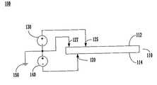
- FIG. 1illustrates an exemplary arrangement of coupling a semiconductor device to a negative voltage, according to an embodiment of the present invention.
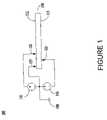
- FIG. 2illustrates a diagram of a method of operating a semiconductor device, according to an embodiment of the present invention.
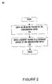
- FIG. 3illustrates a diagram of a method of testing a semiconductor wafer, according to an embodiment of the present invention.
- Embodiments of the present inventionare described in the context of design and operation of integrated semiconductors. More particularly, embodiments of the present invention relate to fractional biasing of semiconductors. It is appreciated, however, that elements of the present invention may be utilized in other areas of semiconductor operation.
- embodiments in accordance with the present inventiondescribe semiconductors formed in p-type materials, it is to be appreciated that symmetries with n-type materials are well known. For example, in general, exchanging p-type materials and processes with n-type materials and processes, and changing voltages from positive to negative can create symmetric structures and behaviors. Consequently, embodiments in accordance with the present invention are well suited to semiconductors formed in n-type materials, and such embodiments are considered within the scope of the present invention.
- a waferIn the process of manufacturing a semiconductor, numerous well-known steps, for example, implantation, thermal annealing, oxide growth and photomask operations, are performed on a wafer. Initially, the wafer comprises a bulk material, for example silicon. The repeated actions of such well-known semiconductor processing upon a wafer generally produces a plurality of layers which constitute an integrated circuit. For the most part, these processing operations are performed on, or directed to, one side (or surface) of a wafer. This side is conventionally known as the “top” of a wafer. It is appreciated that sometimes operations are performed on the “bottom” of a wafer, e.g., lapping to reduce a wafer thickness.
- bottom side processingis generally limited, and semiconductor devices are rarely constructed in or on the “bottom.”
- the term “primary”will be used to represent or describe that surface of a wafer conventionally known as the top surface; for example, it is that surface receiving substantial processing.
- the term “secondary”will represent or describe the other or bottom surface.
- testingtypically involves placing a wafer in a test fixture. While in the test fixture, probe devices, or wafer probes, make contact with particular locations on a wafer. As a wafer typically comprises numerous instances of a semiconductor design, a set of probes is frequently assigned to each instance of the design.
- Wafer testingtypically involves applying a series of electrical stimuli known as test vectors to particular points of an integrated circuit. Proper function may be observed by determining a series of voltages produced by the integrated circuit in response to the test vectors.
- Wafer testingis valuable, in part, because the packaging process is expensive, in the form of packaging materials, operating expenses and capacity of process equipment. If a packaged semiconductor is determined to be non-functional after packaging, the expense of packaging is lost. In addition, certain aspects or nodes of a design may not be testable after packaging. For example, such points may only be available via pads that are generally not bonded out. Determining that a semiconductor is non functional, or likely to be non-functional, at the wafer level, prior to packaging, avoids such costs. Process yield at wafer test is an important metric of the manufacturing process and is often a critical factor in the commercial success of a product.
- the novel coupling of a small negative voltage of less than about 50 mV, for example, negative 15 mV, to the secondary side of a semiconductor devicemay beneficially improve the performance of the semiconductor device. For example, all instances (sites) of a design on a particular wafer may fail the wafer's test vectors in a conventional wafer test. When a slight negative voltage, or back bias, is applied to the secondary surface of the same wafer, all sites were observed to pass the same set of test vectors.
- yield at wafer testis advantageously increased.
- the siteis discarded. For example, it may be marked, e.g., with ink dots, so as not to be used. Frequently, other sites from the wafer may pass wafer testing and proceed to other manufacturing steps. According to an embodiment of the present invention, sites that would have been discarded under the conventional art may now be beneficially used, resulting in increased process yields.
- packaged integrated circuitsmay demonstrate improved performance if a negative voltage is applied to the substrate.
- a negative voltagee.g., negative 15 mV
- Embodiments of the present inventionare well suited to a variety of methods of coupling a negative voltage to a substrate, including coupling to the secondary side of the integrated circuit, back bonding, die bonding, and coupling a voltage to a substrate via conventional bonding pads on the primary surface of an integrated circuit.
- FIG. 1illustrates an exemplary arrangement 100 of coupling a semiconductor device to a negative voltage, according to an embodiment of the present invention.
- Wafer 110comprises a bulk material, for example p-type silicon.
- Wafer 110has been processed, e.g., implanted, doped, annealed, etc., to form a plurality of desirable semiconductor devices within and/or upon wafer 110 .
- the repeated actions of such well-known semiconductor processing upon a wafergenerally produces a plurality of layers which constitute an integrated circuit.
- Wafer 110comprises a primary surface 112 which received substantially all such processing.
- Wafer 110also comprises a secondary surface 114 .
- Wafer 110is coupled to an operating voltage, e.g., 3.0 volts, generated by voltage source 130 via positive probe 125 on primary surface 112 .
- Wafer 110is coupled to a ground reference 150 through ground probe 127 , typically disposed on primary surface 112 .
- performance characteristics of semiconductor devices of wafer 110may be improved by coupling a negative voltage, e.g., minus 15 mV, generated by negative voltage source 140 , via negative probe 120 to secondary surface 114 .
- a ground probee.g., ground probe 127
- This novel coupling of a negative voltage to the secondary side of a semiconductordefines a bias to PN junctions and aligns charge carriers. For example, it defines an unambiguous state for electrical characteristics of a semiconductor. According to embodiments of the present invention, this biasing can produce heretofore unreported benefits in electrical operating characteristics of semiconductors.
- novel coupling of a negative voltage to the secondary side of a semiconductorcan also vacate depletion regions of semiconductor devices.
- the threshold voltage of field effect transistorsis increased, producing multiple beneficial effects, including an advantageous decrease in leakage current.
- parasitic field transistors under a field oxidecan have their threshold voltage increased, beneficially reducing their deleterious effects upon an integrated circuit.
- embodiments of the present inventionare also well suited to a symmetrical arrangement of materials and voltages.
- a symmetric arrangement to that illustrated in FIG. 1would show coupling a positive voltage to the secondary side of a wafer comprising n-type bulk material.
- FIG. 2illustrates a diagram of a method 200 of operating a semiconductor device, according to an embodiment of the present invention.
- an operating voltageis applied to the semiconductor device.
- the operating voltageis frequently designated as Vss or Vcc.
- Such operating voltagesare typically applied to metalized pads on the primary surface of a semiconductor. These pads may be coupled to external package pins, for example, via a wirebonded leadframe or tape automated bonding (TAB).
- TABwirebonded leadframe or tape automated bonding
- solder bumpse.g., controlled chip collapse connection (“C4”), are used to couple pads on the primary surface of a semiconductor to a higher level of packaging.
- a negative voltageis applied to a secondary surface of the semiconductor device.
- This voltagecan have a very small magnitude, e.g., 15 mV.
- Embodiments of the present inventionare well suited to a wide variety of couplings to a secondary surface of semiconductor devices, for example, back bonds and die bonds.
- Alternative embodiments of the present inventioncan also include bonding pads and solder bumps disposed on a secondary surface of semiconductor devices.
- electrical characteristics of a semiconductorcan be enhanced.
- such enhancementmay be the difference between fully functional operation and failure of a semiconductor device.
- embodiments of the present inventioncan beneficially increase process yield.
- such enhancementscan advantageously increase speed of operation and/or reduce power consumption.
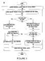
- FIG. 3illustrates a diagram of a method 300 of testing a semiconductor wafer, according to an embodiment of the present invention.
- an integrated circuit waferis received at a testing station.
- the integrated circuit waferhas been processed through a variety of well-known semiconductor processing steps.
- a wafer testing stationtypically comprises equipment to handle a wafer, in addition to a plurality of wafer test probes.
- a positive voltageis applied to the top side of the substrate and the wafer is tested.
- Most integrated circuit devicesutilize a positive operating supply voltage.
- An operating voltageis frequently applied to the top side of a wafer under test.
- Wafer testgenerally comprises applying an operating voltage and ground reference to a wafer.
- Wafer probestypically make contact with various points, e.g., test points, on the wafer. The probes usually excite test points with an electrical waveform. A series of such electrical waveforms is usually referred to as a set of test vectors. Some probes will typically measure a response of an integrated circuit to such test vectors.
- process flowcontinues at optional bock 340 . If the wafer did not pass the test, process flow continues at block 350 .
- a first pass indicatormay be an ink mark, or an identifying number, e.g., a serial number, of the wafer may be recorded in a test database to indicate that the wafer has passed the first test.
- the waferis “binned” or sorted based on the pass indicator.
- the wafermay be placed into a grouping with an indication of when it passed the wafer test, e.g., on a first pass or on a second pass.
- binsmay represent a physical separation. Bins may also represent membership in a list stored in computer readable media.
- a negative voltageis applied to the bottom side of (the wafer's) substrate and the wafer is retested.
- the novel application of a negative voltage to the bottom, or back, side of a waferhas been shown to improve the wafer's operating characteristics.
- test vectors and/or the nature of the testscan be different in block 350 than in block 320 . Additionally, more or less test or test sites may be required to pass in order for the wafer to be determined to pass the testing. If the wafer passed the test, e.g., a set of responses to test vectors substantially matches a set of expected responses for a set of test vectors, process flow continues at optional bock 362 . If the wafer did not pass the test, process flow continues at optional block 364 .
- test of block 350was passed, the wafer is marked with a second pass indicator in optional block 362 . If the test was not passed, control passes from block optional 360 to optional block 364 . In optional block 364 further testing can be performed on the wafer or various sites of the wafer, e.g., to determine a cause of failure, or the wafer can be rejected as defective.
- Process control from either optional block 370 or optional block 364passes to optional block 380 .
- optional block 380the previous steps are repeated until all wafers, e.g., of a production lot, have been tested.
Landscapes
- Engineering & Computer Science (AREA)
- Manufacturing & Machinery (AREA)
- Computer Hardware Design (AREA)
- Microelectronics & Electronic Packaging (AREA)
- Power Engineering (AREA)
- Testing Or Measuring Of Semiconductors Or The Like (AREA)
Abstract
Description
This application is a divisional of and claims priority to U.S. patent Ser. No. 10/769,140 entitled “Fractional Biasing Of Semiconductors,” by Kuei, filed on Jan. 29, 2004 now U.S. Pat. No. 6,943,614, which is incorporated herein by reference.
Embodiments of the present invention relate to the manufacture, test and operation of integrated circuits.
Semiconductor devices, e.g., digital logic integrated circuits are generally operated with a positive supply voltage. A ground reference (or ground return) is typically electrically coupled to the front or primary side of a semiconductor in a fashion similar to the coupling of a main operating voltage. Sometimes, the back or secondary side of a semiconductor is thermally coupled to a heat sink.
A method and system of fractional biasing of semiconductors are disclosed. A small negative voltage is applied to the back of a semiconductor wafer or device. An operating voltage is applied to the semiconductor. Operating characteristics of the semiconductor are enhanced by application of a fractional bias.
In the following detailed description of the present invention, fractional biasing of semiconductors, numerous specific details are set forth in order to provide a thorough understanding of the present invention. However, it will be recognized by one skilled in the art that the present invention may be practiced without these specific details or with equivalents thereof. In other instances, well-known methods, procedures, components, and circuits have not been described in detail as not to unnecessarily obscure aspects of the present invention.
Some portions of the detailed descriptions which follow (e.g.,processes 200 and300) are presented in terms of procedures, steps, logic blocks, processing, and other symbolic representations of operations on data bits that can be performed on computer memory. These descriptions and representations are the means used by those skilled in the data processing arts to most effectively convey the substance of their work to others skilled in the art. A procedure, computer executed step, logic block, process, etc., is here, and generally, conceived to be a self-consistent sequence of steps or instructions or firmware leading to a desired result. The steps are those requiring physical manipulations of physical quantities. Usually, though not necessarily, these quantities take the form of electrical or magnetic signals capable of being stored, transferred, combined, compared, and otherwise manipulated in a computer system. It has proven convenient at times, principally for reasons of common usage, to refer to these signals as bits, values, elements, symbols, characters, terms, numbers, or the like.
It should be borne in mind, however, that all of these and similar terms are to be associated with the appropriate physical quantities and are merely convenient labels applied to these quantities. Unless specifically stated otherwise as apparent from the following discussions, it is appreciated that throughout the present invention, discussions utilizing terms such as “accessing” or “indexing” or “processing” or “computing” or “translating” or “calculating” or “determining” or “selecting” or “storing” or “recognizing” or “generating” or “selecting” or “moving” or “encoding” or “combining” or “testing” of “setting” or “operating” or “transforming” or “determining” or “optimizing” or “synthesizing” or “grouping” or “estimating” or “describing” or “measuring” or “recording” or “associating” or the like, refer to the action and processes of a computer system, or similar electronic computing device, that manipulates and transforms data represented as physical (electronic) quantities within the computer system's registers and memories into other data similarly represented as physical quantities within the computer system memories or registers or other such information storage, transmission or display devices.
Embodiments of the present invention are described in the context of design and operation of integrated semiconductors. More particularly, embodiments of the present invention relate to fractional biasing of semiconductors. It is appreciated, however, that elements of the present invention may be utilized in other areas of semiconductor operation.
Although the following description of embodiments in accordance with the present invention describes semiconductors formed in p-type materials, it is to be appreciated that symmetries with n-type materials are well known. For example, in general, exchanging p-type materials and processes with n-type materials and processes, and changing voltages from positive to negative can create symmetric structures and behaviors. Consequently, embodiments in accordance with the present invention are well suited to semiconductors formed in n-type materials, and such embodiments are considered within the scope of the present invention.
In the process of manufacturing a semiconductor, numerous well-known steps, for example, implantation, thermal annealing, oxide growth and photomask operations, are performed on a wafer. Initially, the wafer comprises a bulk material, for example silicon. The repeated actions of such well-known semiconductor processing upon a wafer generally produces a plurality of layers which constitute an integrated circuit. For the most part, these processing operations are performed on, or directed to, one side (or surface) of a wafer. This side is conventionally known as the “top” of a wafer. It is appreciated that sometimes operations are performed on the “bottom” of a wafer, e.g., lapping to reduce a wafer thickness. However, such “bottom side” processing is generally limited, and semiconductor devices are rarely constructed in or on the “bottom.” Hereinafter, the term “primary” will be used to represent or describe that surface of a wafer conventionally known as the top surface; for example, it is that surface receiving substantial processing. The term “secondary” will represent or describe the other or bottom surface.
Conventionally, following a manufacturing process, a semiconductor wafer is tested. Testing typically involves placing a wafer in a test fixture. While in the test fixture, probe devices, or wafer probes, make contact with particular locations on a wafer. As a wafer typically comprises numerous instances of a semiconductor design, a set of probes is frequently assigned to each instance of the design.
Testing at the wafer level is generally intended to determine which instances of a semiconductor design on a wafer are likely to be functional and which instances are unlikely to perform correctly. A final determination of functionality may not be made until after further manufacturing steps, for example, cutting into individual die and final packaging. Wafer testing typically involves applying a series of electrical stimuli known as test vectors to particular points of an integrated circuit. Proper function may be observed by determining a series of voltages produced by the integrated circuit in response to the test vectors.
Wafer testing is valuable, in part, because the packaging process is expensive, in the form of packaging materials, operating expenses and capacity of process equipment. If a packaged semiconductor is determined to be non-functional after packaging, the expense of packaging is lost. In addition, certain aspects or nodes of a design may not be testable after packaging. For example, such points may only be available via pads that are generally not bonded out. Determining that a semiconductor is non functional, or likely to be non-functional, at the wafer level, prior to packaging, avoids such costs. Process yield at wafer test is an important metric of the manufacturing process and is often a critical factor in the commercial success of a product.
It is usually the case that all wafer probes contact the primary surface of a wafer. Some semiconductors are designed such that the secondary surface of the wafer (or die) should be grounded for operation. In such cases, it is well known to contact the secondary surface of a wafer under test in order to ground the wafer. It is to be appreciated however, that such ground connections are typically made to the primary side of a wafer, and coupled within the wafer to the substrate.
It is also known to couple the secondary surface of a wafer or die to ground during operation. Such couplings as back bonding or die bonding may couple a secondary surface of a wafer to ground as well as provide for thermal dissipation.
According to an embodiment of the present invention, the novel coupling of a small negative voltage of less than about 50 mV, for example, negative 15 mV, to the secondary side of a semiconductor device may beneficially improve the performance of the semiconductor device. For example, all instances (sites) of a design on a particular wafer may fail the wafer's test vectors in a conventional wafer test. When a slight negative voltage, or back bias, is applied to the secondary surface of the same wafer, all sites were observed to pass the same set of test vectors.
As a beneficial result of applying a small negative voltage to the secondary side of a wafer, yield at wafer test is advantageously increased.
It is generally the case that if an instance of a semiconductor design, or site, does not function (as determined by results of wafer test vectors) at wafer test, the site is discarded. For example, it may be marked, e.g., with ink dots, so as not to be used. Frequently, other sites from the wafer may pass wafer testing and proceed to other manufacturing steps. According to an embodiment of the present invention, sites that would have been discarded under the conventional art may now be beneficially used, resulting in increased process yields.
In a similar manner, packaged integrated circuits may demonstrate improved performance if a negative voltage is applied to the substrate. For example, if a packaged semiconductor does not pass its test vectors, the application of a negative voltage, e.g., negative 15 mV, has been demonstrated to beneficially cause the same device to pass the same vectors. Embodiments of the present invention are well suited to a variety of methods of coupling a negative voltage to a substrate, including coupling to the secondary side of the integrated circuit, back bonding, die bonding, and coupling a voltage to a substrate via conventional bonding pads on the primary surface of an integrated circuit.
The beneficial effects of small “fractional” biases applied to the secondary surface of a wafer are heretofore unreported. For example, conventional bias voltages applied to modern deep sub micron semiconductors could be in the range of 0.2 volts to 1.0 volts. A bias voltage of 1.0 volts can increase the threshold voltage by about 100 mV and reduce transistor leakage current by about a factor of 10. In comparison, a bias voltage that is a fraction of conventional bias voltages, e.g., 50 mV, would shift the same threshold voltage by only 5 mV and decrease leakage current by about 15%. Such changes are roughly equivalent to a 5 degree Celsius change in junction temperature. Conventionally, such small changes were not believed to be significant to the operation of semiconductors. Beneficial effects of fractional biases, e.g., a difference between functional and non functional integrated circuits, are surprising and novel.
This novel coupling of a negative voltage to the secondary side of a semiconductor defines a bias to PN junctions and aligns charge carriers. For example, it defines an unambiguous state for electrical characteristics of a semiconductor. According to embodiments of the present invention, this biasing can produce heretofore unreported benefits in electrical operating characteristics of semiconductors.
In addition, novel coupling of a negative voltage to the secondary side of a semiconductor can also vacate depletion regions of semiconductor devices. Further, the threshold voltage of field effect transistors is increased, producing multiple beneficial effects, including an advantageous decrease in leakage current. Further still, parasitic field transistors under a field oxide can have their threshold voltage increased, beneficially reducing their deleterious effects upon an integrated circuit.
It is to be appreciated that embodiments of the present invention are also well suited to a symmetrical arrangement of materials and voltages. For example, a symmetric arrangement to that illustrated inFIG. 1 would show coupling a positive voltage to the secondary side of a wafer comprising n-type bulk material.
Inblock 210, an operating voltage is applied to the semiconductor device. The operating voltage is frequently designated as Vss or Vcc. Such operating voltages are typically applied to metalized pads on the primary surface of a semiconductor. These pads may be coupled to external package pins, for example, via a wirebonded leadframe or tape automated bonding (TAB). Sometimes, solder bumps, e.g., controlled chip collapse connection (“C4”), are used to couple pads on the primary surface of a semiconductor to a higher level of packaging.
Inblock 220, a negative voltage is applied to a secondary surface of the semiconductor device. This voltage can have a very small magnitude, e.g., 15 mV. Embodiments of the present invention are well suited to a wide variety of couplings to a secondary surface of semiconductor devices, for example, back bonds and die bonds. Alternative embodiments of the present invention can also include bonding pads and solder bumps disposed on a secondary surface of semiconductor devices.
In this novel manner, electrical characteristics of a semiconductor can be enhanced. In some cases, such enhancement may be the difference between fully functional operation and failure of a semiconductor device. In such cases, embodiments of the present invention can beneficially increase process yield. In other cases, such enhancements can advantageously increase speed of operation and/or reduce power consumption.
Inblock 320, a positive voltage is applied to the top side of the substrate and the wafer is tested. Most integrated circuit devices utilize a positive operating supply voltage. An operating voltage is frequently applied to the top side of a wafer under test. Wafer test generally comprises applying an operating voltage and ground reference to a wafer. Wafer probes typically make contact with various points, e.g., test points, on the wafer. The probes usually excite test points with an electrical waveform. A series of such electrical waveforms is usually referred to as a set of test vectors. Some probes will typically measure a response of an integrated circuit to such test vectors.
Inblock 330, it is determined if the wafer passed the test. This is usually determined by comparing measured responses of a wafer with a set of expected responses for a set of test vectors. If the wafer passed the test, e.g., a set of responses to test vectors substantially matches a set of expected responses for a set of test vectors, process flow continues atoptional bock 340. If the wafer did not pass the test, process flow continues atblock 350.
If process flow continues atoptional bock 340, the wafer is marked with a first pass indicator. A first pass indicator may be an ink mark, or an identifying number, e.g., a serial number, of the wafer may be recorded in a test database to indicate that the wafer has passed the first test.
After marking, inoptional block 370 the wafer is “binned” or sorted based on the pass indicator. For example, the wafer may be placed into a grouping with an indication of when it passed the wafer test, e.g., on a first pass or on a second pass. It is to be appreciated that a wide variety of “binning” methods are well suited to embodiments in accordance with the present invention. For example, bins may represent a physical separation. Bins may also represent membership in a list stored in computer readable media.
If the wafer did not pass the test inblock 330, control passes to block350. Inblock 350, a negative voltage is applied to the bottom side of (the wafer's) substrate and the wafer is retested. The novel application of a negative voltage to the bottom, or back, side of a wafer has been shown to improve the wafer's operating characteristics.
Inoptional block 360, it is determined if the wafer passed the test. This determination may be made using substantially the same criteria as were used in block330 (above). It is appreciated that embodiments in accordance with the present invention are well suited to the use of alternative criteria for passing. For example, the test vectors and/or the nature of the tests can be different inblock 350 than inblock 320. Additionally, more or less test or test sites may be required to pass in order for the wafer to be determined to pass the testing. If the wafer passed the test, e.g., a set of responses to test vectors substantially matches a set of expected responses for a set of test vectors, process flow continues atoptional bock 362. If the wafer did not pass the test, process flow continues atoptional block 364.
If the test ofblock 350 was passed, the wafer is marked with a second pass indicator inoptional block 362. If the test was not passed, control passes from block optional360 tooptional block 364. Inoptional block 364 further testing can be performed on the wafer or various sites of the wafer, e.g., to determine a cause of failure, or the wafer can be rejected as defective.
Process control from eitheroptional block 370 oroptional block 364 passes tooptional block 380. Inoptional block 380 the previous steps are repeated until all wafers, e.g., of a production lot, have been tested.
The preferred embodiment of the present invention, fractional biasing of semiconductors, is thus described. While the present invention has been described in particular embodiments, it should be appreciated that the present invention should not be construed as limited by such embodiments, but rather construed according to the below claims.
Claims (17)
1. A semiconductor device comprising:
a primary surface of bulk material coupled to a supply voltage source through a positive and a negative terminal of the supply voltage source, wherein the negative terminal is also coupled to ground;
a back surface of the bulk material substantially parallel to the primary surface, wherein the back surface is configured to receive a fractional negative voltage as a body bias and wherein the fractional negative voltage is a fraction of a standard bias voltage;
a voltage source that is coupled to the semiconductor device to supply the fractional negative voltage; and
a coupling for conducting the fractional negative voltage to the back surface wherein the fractional negative voltage is less than about 50 millivolts in magnitude.
2. The semiconductor device ofclaim 1 wherein the bulk material is silicon.
3. The semiconductor device ofclaim 2 wherein the silicon comprises a plurality of layers which constitute an integrated circuit.
4. The semiconductor device ofclaim 1 further comprising circuitry to generate the fractional negative voltage.
5. The semiconductor device ofclaim 1 wherein the fractional negative voltage is generated external to the semiconductor device.
6. The semiconductor device ofclaim 1 wherein the bulk material is silicon, and the silicon comprises a plurality of layers which constitute an integrated circuit.
7. A device comprising:
a primary surface of a substrate comprising an integrated circuit and coupled to a supply voltage source through a positive and a negative terminal of the supply voltage source, wherein the negative terminal is also coupled to ground;
a back surface of the substrate substantially opposed to the primary surface, wherein the back surface is configured to receive a fractional negative voltage as a body bias and wherein the fractional negative voltage is a fraction of a standard bias voltage;
a coupling for conducting the fractional negative voltage to the back surface; and
a voltage source to supply the fractional negative voltage wherein the fractional negative voltage is less than about 50 millivolts in magnitude.
8. A device comprising:
a primary surface of a substrate comprising an integrated circuit that receives an operating voltage from a supply voltage source that comprises a positive and a negative terminal wherein the positive and the negative terminal are coupled to the primary surface of the substrate and the positive terminal is also coupled to ground, and wherein the primary surface is configured to receive a negative operating voltage for the integrated circuit;
a second surface of the substrate substantially opposed to the primary surface of the substrate, wherein the second surface is configured to receive a fractional positive voltage as a body bias and wherein the fractional positive voltage is a fraction of a standard bias voltage;
a voltage source that is coupled to the device to supply the fractional positive voltage; and
a coupling for conducting the fractional positive voltage to the second surface wherein the fractional positive voltage is less than about 50 millivolts in magnitude.
9. The device ofclaim 7 wherein the substrate is silicon.
10. The device ofclaim 9 wherein the silicon comprises a plurality of layers which constitute the integrated circuit.
11. The device ofclaim 7 wherein the fractional negative voltage is generated external to the semiconductor device.
12. The device ofclaim 8 wherein the substrate is silicon.
13. The device ofclaim 8 wherein the silicon comprises a plurality of layers which constitute the integrated circuit.
14. The device ofclaim 8 wherein the fractional negative voltage is generated external to the semiconductor device.
15. A method comprising:
supplying respective voltages from a positive and a negative terminal of a first voltage source to a primary surface of semiconductor bulk material wherein the positive and the negative terminal of the first voltage source are coupled to the primary surface of the bulk material and the negative terminal of the first voltage source is also coupled to ground; and
supplying a fractional negative voltage of less than 50 millivolts as a body bias to a back surface of the semiconductor bulk material from a negative terminal of a second voltage source, wherein the back surface of the semiconductor bulk material is substantially parallel to the primary surface.
16. The method ofclaim 15 further comprising measuring a response of said semiconductor bulk material to the supplying respective voltages and the supplying the fractional negative voltage.
17. The method ofclaim 16 further comprising determining if an integrated circuit associated with the bulk material is operating properly by comparing the response with an expected response.
Priority Applications (1)
| Application Number | Priority Date | Filing Date | Title |
|---|---|---|---|
| US11/199,985US7705350B1 (en) | 2004-01-29 | 2005-08-08 | Fractional biasing of semiconductors |
Applications Claiming Priority (2)
| Application Number | Priority Date | Filing Date | Title |
|---|---|---|---|
| US10/769,140US6943614B1 (en) | 2004-01-29 | 2004-01-29 | Fractional biasing of semiconductors |
| US11/199,985US7705350B1 (en) | 2004-01-29 | 2005-08-08 | Fractional biasing of semiconductors |
Related Parent Applications (1)
| Application Number | Title | Priority Date | Filing Date |
|---|---|---|---|
| US10/769,140DivisionUS6943614B1 (en) | 2004-01-29 | 2004-01-29 | Fractional biasing of semiconductors |
Publications (1)
| Publication Number | Publication Date |
|---|---|
| US7705350B1true US7705350B1 (en) | 2010-04-27 |
Family
ID=34911298
Family Applications (2)
| Application Number | Title | Priority Date | Filing Date |
|---|---|---|---|
| US10/769,140Expired - LifetimeUS6943614B1 (en) | 2004-01-29 | 2004-01-29 | Fractional biasing of semiconductors |
| US11/199,985Expired - Fee RelatedUS7705350B1 (en) | 2004-01-29 | 2005-08-08 | Fractional biasing of semiconductors |
Family Applications Before (1)
| Application Number | Title | Priority Date | Filing Date |
|---|---|---|---|
| US10/769,140Expired - LifetimeUS6943614B1 (en) | 2004-01-29 | 2004-01-29 | Fractional biasing of semiconductors |
Country Status (1)
| Country | Link |
|---|---|
| US (2) | US6943614B1 (en) |
Families Citing this family (5)
| Publication number | Priority date | Publication date | Assignee | Title |
|---|---|---|---|---|
| US20070139098A1 (en)* | 2005-12-15 | 2007-06-21 | P.A. Semi, Inc. | Wearout compensation mechanism using back bias technique |
| US9854372B2 (en)* | 2015-08-29 | 2017-12-26 | Bragi GmbH | Production line PCB serial programming and testing method and system |
| US9843853B2 (en) | 2015-08-29 | 2017-12-12 | Bragi GmbH | Power control for battery powered personal area network device system and method |
| US10104458B2 (en) | 2015-10-20 | 2018-10-16 | Bragi GmbH | Enhanced biometric control systems for detection of emergency events system and method |
| US10344960B2 (en) | 2017-09-19 | 2019-07-09 | Bragi GmbH | Wireless earpiece controlled medical headlight |
Citations (26)
| Publication number | Priority date | Publication date | Assignee | Title |
|---|---|---|---|---|
| US3760202A (en)* | 1971-01-14 | 1973-09-18 | Rca Corp | Input circuits for charged-coupled circuits |
| US4014779A (en) | 1974-11-01 | 1977-03-29 | Coulter Information Systems, Inc. | Sputtering apparatus |
| US4134124A (en)* | 1976-11-27 | 1979-01-09 | Ferranti Limited | Semiconductor devices and circuit arrangements including such devices |
| US4471289A (en) | 1983-03-04 | 1984-09-11 | Ncr Corporation | Switching power supply circuit |
| US4814288A (en)* | 1986-07-14 | 1989-03-21 | Hitachi, Ltd. | Method of fabricating semiconductor devices which include vertical elements and control elements |
| US5264723A (en)* | 1992-04-09 | 1993-11-23 | At&T Bell Laboratories | Integrated circuit with MOS capacitor for improved ESD protection |
| US5289029A (en)* | 1991-05-02 | 1994-02-22 | Nec Corporation | Semiconductor integrated circuit device having wells biased with different voltage levels |
| US5374839A (en)* | 1992-10-31 | 1994-12-20 | Samsung Electronics Co., Ltd. | Semiconductor memory device |
| US6018177A (en)* | 1998-02-04 | 2000-01-25 | Vanguard International Semiconductor Corporation | DRAM cell and array to store two-bit data |
| US6049479A (en)* | 1999-09-23 | 2000-04-11 | Advanced Micro Devices, Inc. | Operational approach for the suppression of bi-directional tunnel oxide stress of a flash cell |
| US6048746A (en) | 1998-06-08 | 2000-04-11 | Sun Microsystems, Inc. | Method for making die-compensated threshold tuning circuit |
| US6087892A (en) | 1998-06-08 | 2000-07-11 | Sun Microsystems, Inc. | Target Ion/Ioff threshold tuning circuit and method |
| US6091283A (en) | 1998-02-24 | 2000-07-18 | Sun Microsystems, Inc. | Sub-threshold leakage tuning circuit |
| US6184548B1 (en)* | 1998-02-04 | 2001-02-06 | Vanguard International Semiconductor Corporation | DRAM cell and array to store two-bit data having merged stack capacitor and trench capacitor |
| US6188234B1 (en)* | 1999-01-07 | 2001-02-13 | International Business Machines Corporation | Method of determining dielectric time-to-breakdown |
| US6218708B1 (en) | 1998-02-25 | 2001-04-17 | Sun Microsystems, Inc. | Back-biased MOS device and method |
| US6303444B1 (en) | 2000-10-19 | 2001-10-16 | Sun Microsystems, Inc. | Method for introducing an equivalent RC circuit in a MOS device using resistive wells |
| US6330190B1 (en)* | 1996-05-30 | 2001-12-11 | Hyundai Electronics America | Semiconductor structure for flash memory enabling low operating potentials |
| US6489224B1 (en) | 2001-05-31 | 2002-12-03 | Sun Microsystems, Inc. | Method for engineering the threshold voltage of a device using buried wells |
| US20030012054A1 (en)* | 1998-08-27 | 2003-01-16 | Kim Jin-Woo | Methods of operating semiconductor memory devices having split gate-type non-volatile memory cells |
| US20040000692A1 (en)* | 2002-06-27 | 2004-01-01 | Sumitomo Electric Industires, Ltd. | Method and device for determining backgate characteristics |
| US6906953B2 (en)* | 2002-06-21 | 2005-06-14 | Micron Technology, Inc. | Vertical NROM having a storage density of 1 bit per 1F2 |
| US20060076418A1 (en)* | 2002-11-21 | 2006-04-13 | Koninlijke Philips Electronics N.V. | Electronic memory component or memory module, and method of operating same |
| US20060175656A1 (en)* | 2001-04-27 | 2006-08-10 | Interuniversitair Microelektronica Centrum (Imec Vzw) | Non-volatile memory devices |
| US7115427B2 (en)* | 2004-08-25 | 2006-10-03 | Atomic Energy Council - Institute Of Nuclear Energy Research | Red light-emitting device and method for preparing the same |
| US20060261404A1 (en)* | 2003-12-17 | 2006-11-23 | Micron Technology, Inc. | Vertical NROM NAND flash memory array |
- 2004
- 2004-01-29USUS10/769,140patent/US6943614B1/ennot_activeExpired - Lifetime
- 2005
- 2005-08-08USUS11/199,985patent/US7705350B1/ennot_activeExpired - Fee Related
Patent Citations (26)
| Publication number | Priority date | Publication date | Assignee | Title |
|---|---|---|---|---|
| US3760202A (en)* | 1971-01-14 | 1973-09-18 | Rca Corp | Input circuits for charged-coupled circuits |
| US4014779A (en) | 1974-11-01 | 1977-03-29 | Coulter Information Systems, Inc. | Sputtering apparatus |
| US4134124A (en)* | 1976-11-27 | 1979-01-09 | Ferranti Limited | Semiconductor devices and circuit arrangements including such devices |
| US4471289A (en) | 1983-03-04 | 1984-09-11 | Ncr Corporation | Switching power supply circuit |
| US4814288A (en)* | 1986-07-14 | 1989-03-21 | Hitachi, Ltd. | Method of fabricating semiconductor devices which include vertical elements and control elements |
| US5289029A (en)* | 1991-05-02 | 1994-02-22 | Nec Corporation | Semiconductor integrated circuit device having wells biased with different voltage levels |
| US5264723A (en)* | 1992-04-09 | 1993-11-23 | At&T Bell Laboratories | Integrated circuit with MOS capacitor for improved ESD protection |
| US5374839A (en)* | 1992-10-31 | 1994-12-20 | Samsung Electronics Co., Ltd. | Semiconductor memory device |
| US6330190B1 (en)* | 1996-05-30 | 2001-12-11 | Hyundai Electronics America | Semiconductor structure for flash memory enabling low operating potentials |
| US6018177A (en)* | 1998-02-04 | 2000-01-25 | Vanguard International Semiconductor Corporation | DRAM cell and array to store two-bit data |
| US6184548B1 (en)* | 1998-02-04 | 2001-02-06 | Vanguard International Semiconductor Corporation | DRAM cell and array to store two-bit data having merged stack capacitor and trench capacitor |
| US6091283A (en) | 1998-02-24 | 2000-07-18 | Sun Microsystems, Inc. | Sub-threshold leakage tuning circuit |
| US6218708B1 (en) | 1998-02-25 | 2001-04-17 | Sun Microsystems, Inc. | Back-biased MOS device and method |
| US6048746A (en) | 1998-06-08 | 2000-04-11 | Sun Microsystems, Inc. | Method for making die-compensated threshold tuning circuit |
| US6087892A (en) | 1998-06-08 | 2000-07-11 | Sun Microsystems, Inc. | Target Ion/Ioff threshold tuning circuit and method |
| US20030012054A1 (en)* | 1998-08-27 | 2003-01-16 | Kim Jin-Woo | Methods of operating semiconductor memory devices having split gate-type non-volatile memory cells |
| US6188234B1 (en)* | 1999-01-07 | 2001-02-13 | International Business Machines Corporation | Method of determining dielectric time-to-breakdown |
| US6049479A (en)* | 1999-09-23 | 2000-04-11 | Advanced Micro Devices, Inc. | Operational approach for the suppression of bi-directional tunnel oxide stress of a flash cell |
| US6303444B1 (en) | 2000-10-19 | 2001-10-16 | Sun Microsystems, Inc. | Method for introducing an equivalent RC circuit in a MOS device using resistive wells |
| US20060175656A1 (en)* | 2001-04-27 | 2006-08-10 | Interuniversitair Microelektronica Centrum (Imec Vzw) | Non-volatile memory devices |
| US6489224B1 (en) | 2001-05-31 | 2002-12-03 | Sun Microsystems, Inc. | Method for engineering the threshold voltage of a device using buried wells |
| US6906953B2 (en)* | 2002-06-21 | 2005-06-14 | Micron Technology, Inc. | Vertical NROM having a storage density of 1 bit per 1F2 |
| US20040000692A1 (en)* | 2002-06-27 | 2004-01-01 | Sumitomo Electric Industires, Ltd. | Method and device for determining backgate characteristics |
| US20060076418A1 (en)* | 2002-11-21 | 2006-04-13 | Koninlijke Philips Electronics N.V. | Electronic memory component or memory module, and method of operating same |
| US20060261404A1 (en)* | 2003-12-17 | 2006-11-23 | Micron Technology, Inc. | Vertical NROM NAND flash memory array |
| US7115427B2 (en)* | 2004-08-25 | 2006-10-03 | Atomic Energy Council - Institute Of Nuclear Energy Research | Red light-emitting device and method for preparing the same |
Also Published As
| Publication number | Publication date |
|---|---|
| US6943614B1 (en) | 2005-09-13 |
Similar Documents
| Publication | Publication Date | Title |
|---|---|---|
| US10161965B2 (en) | Method of test probe alignment control | |
| CN1926439B (en) | System and method for reducing temperature variation during burn-in | |
| US7307441B2 (en) | Integrated circuit chips and wafers including on-chip test element group circuits, and methods of fabricating and testing same | |
| US5532610A (en) | Apparatus for testing semicondctor wafer | |
| JP4359576B2 (en) | Method for disposing chip of first substrate on second substrate | |
| US9188631B2 (en) | Element substrate, inspecting method, and manufacturing method of semiconductor device | |
| JPH075231A (en) | Method and apparatus for screening of reliability of semiconductor circuit | |
| US20060181297A1 (en) | Method and Apparatus for Non-Invasively Testing Integrated Circuits | |
| CN102169869B (en) | Reliability test structure and method for detecting crystal orientation correlation of MOS devices | |
| CN102253324A (en) | Testing structure and testing method for hot carrier effect of MOS (Metal Oxide Semiconductor) device | |
| US7825678B2 (en) | Test pad design for reducing the effect of contact resistances | |
| US7705350B1 (en) | Fractional biasing of semiconductors | |
| US9696376B2 (en) | Leakage testing of integrated circuits using a logarithmic transducer and a voltmeter | |
| CN113889421A (en) | Screening method and apparatus for detecting deep trench isolation and SOI defects | |
| US20230168297A1 (en) | Localized heating/cooling using thermocouple between probe pins | |
| US10234499B1 (en) | Integrated circuit testing using on-chip electrical test structure | |
| JPH10178073A (en) | Inspection method and semiconductor device manufacturing method | |
| Mizumura et al. | Study of 90-nm MOSFET subthreshold hump characteristics using newly developed MOSFET array test structure | |
| US7106084B2 (en) | Method of screening semiconductor device | |
| US11257723B2 (en) | Inspection system and method for inspecting semiconductor package, and method of fabricating semiconductor package | |
| JP2000039461A (en) | Measuring method for junction temperature of semiconductor integrated circuit and dut board using the measuring method | |
| Niewczas | Characterisation of the threshold voltage variation: a test chip and the results | |
| KR100641471B1 (en) | Input IC structure of semiconductor device | |
| Seng et al. | SiC DMOSFET Real Wafer Level HTRB and HTGB Evaluation | |
| KR20000066562A (en) | Semiconductor device for testing a degradation grade by hot carrier effect under ac operation |
Legal Events
| Date | Code | Title | Description |
|---|---|---|---|
| AS | Assignment | Owner name:TRANSMETA LLC,CALIFORNIA Free format text:MERGER;ASSIGNOR:TRANSMETA CORPORATION;REEL/FRAME:022454/0522 Effective date:20090127 Owner name:TRANSMETA LLC, CALIFORNIA Free format text:MERGER;ASSIGNOR:TRANSMETA CORPORATION;REEL/FRAME:022454/0522 Effective date:20090127 | |
| AS | Assignment | Owner name:INTELLECTUAL VENTURE FUNDING LLC,NEVADA Free format text:ASSIGNMENT OF ASSIGNORS INTEREST;ASSIGNOR:TRANSMETA LLC;REEL/FRAME:023268/0771 Effective date:20090128 Owner name:INTELLECTUAL VENTURE FUNDING LLC, NEVADA Free format text:ASSIGNMENT OF ASSIGNORS INTEREST;ASSIGNOR:TRANSMETA LLC;REEL/FRAME:023268/0771 Effective date:20090128 | |
| REMI | Maintenance fee reminder mailed | ||
| LAPS | Lapse for failure to pay maintenance fees | ||
| STCH | Information on status: patent discontinuation | Free format text:PATENT EXPIRED DUE TO NONPAYMENT OF MAINTENANCE FEES UNDER 37 CFR 1.362 | |
| FP | Lapsed due to failure to pay maintenance fee | Effective date:20140427 |