US7703945B2 - Efficient emitting LED package and method for efficiently emitting light - Google Patents
Efficient emitting LED package and method for efficiently emitting lightDownload PDFInfo
- Publication number
- US7703945B2 US7703945B2US11/476,520US47652006AUS7703945B2US 7703945 B2US7703945 B2US 7703945B2US 47652006 AUS47652006 AUS 47652006AUS 7703945 B2US7703945 B2US 7703945B2
- Authority
- US
- United States
- Prior art keywords
- led
- light
- converted
- package
- reflected
- Prior art date
- Legal status (The legal status is an assumption and is not a legal conclusion. Google has not performed a legal analysis and makes no representation as to the accuracy of the status listed.)
- Active, expires
Links
Images


Classifications
- H—ELECTRICITY
- H10—SEMICONDUCTOR DEVICES; ELECTRIC SOLID-STATE DEVICES NOT OTHERWISE PROVIDED FOR
- H10H—INORGANIC LIGHT-EMITTING SEMICONDUCTOR DEVICES HAVING POTENTIAL BARRIERS
- H10H20/00—Individual inorganic light-emitting semiconductor devices having potential barriers, e.g. light-emitting diodes [LED]
- H10H20/80—Constructional details
- H10H20/85—Packages
- H10H20/851—Wavelength conversion means
- H10H20/8515—Wavelength conversion means not being in contact with the bodies
- F—MECHANICAL ENGINEERING; LIGHTING; HEATING; WEAPONS; BLASTING
- F21—LIGHTING
- F21K—NON-ELECTRIC LIGHT SOURCES USING LUMINESCENCE; LIGHT SOURCES USING ELECTROCHEMILUMINESCENCE; LIGHT SOURCES USING CHARGES OF COMBUSTIBLE MATERIAL; LIGHT SOURCES USING SEMICONDUCTOR DEVICES AS LIGHT-GENERATING ELEMENTS; LIGHT SOURCES NOT OTHERWISE PROVIDED FOR
- F21K9/00—Light sources using semiconductor devices as light-generating elements, e.g. using light-emitting diodes [LED] or lasers
- F21K9/60—Optical arrangements integrated in the light source, e.g. for improving the colour rendering index or the light extraction
- F21K9/64—Optical arrangements integrated in the light source, e.g. for improving the colour rendering index or the light extraction using wavelength conversion means distinct or spaced from the light-generating element, e.g. a remote phosphor layer
- F—MECHANICAL ENGINEERING; LIGHTING; HEATING; WEAPONS; BLASTING
- F21—LIGHTING
- F21V—FUNCTIONAL FEATURES OR DETAILS OF LIGHTING DEVICES OR SYSTEMS THEREOF; STRUCTURAL COMBINATIONS OF LIGHTING DEVICES WITH OTHER ARTICLES, NOT OTHERWISE PROVIDED FOR
- F21V13/00—Producing particular characteristics or distribution of the light emitted by means of a combination of elements specified in two or more of main groups F21V1/00 - F21V11/00
- F21V13/02—Combinations of only two kinds of elements
- F21V13/04—Combinations of only two kinds of elements the elements being reflectors and refractors
- F—MECHANICAL ENGINEERING; LIGHTING; HEATING; WEAPONS; BLASTING
- F21—LIGHTING
- F21V—FUNCTIONAL FEATURES OR DETAILS OF LIGHTING DEVICES OR SYSTEMS THEREOF; STRUCTURAL COMBINATIONS OF LIGHTING DEVICES WITH OTHER ARTICLES, NOT OTHERWISE PROVIDED FOR
- F21V7/00—Reflectors for light sources
- F21V7/0008—Reflectors for light sources providing for indirect lighting
- F—MECHANICAL ENGINEERING; LIGHTING; HEATING; WEAPONS; BLASTING
- F21—LIGHTING
- F21V—FUNCTIONAL FEATURES OR DETAILS OF LIGHTING DEVICES OR SYSTEMS THEREOF; STRUCTURAL COMBINATIONS OF LIGHTING DEVICES WITH OTHER ARTICLES, NOT OTHERWISE PROVIDED FOR
- F21V7/00—Reflectors for light sources
- F21V7/0025—Combination of two or more reflectors for a single light source
- F21V7/0033—Combination of two or more reflectors for a single light source with successive reflections from one reflector to the next or following
- F—MECHANICAL ENGINEERING; LIGHTING; HEATING; WEAPONS; BLASTING
- F21—LIGHTING
- F21V—FUNCTIONAL FEATURES OR DETAILS OF LIGHTING DEVICES OR SYSTEMS THEREOF; STRUCTURAL COMBINATIONS OF LIGHTING DEVICES WITH OTHER ARTICLES, NOT OTHERWISE PROVIDED FOR
- F21V7/00—Reflectors for light sources
- F21V7/22—Reflectors for light sources characterised by materials, surface treatments or coatings, e.g. dichroic reflectors
- F21V7/24—Reflectors for light sources characterised by materials, surface treatments or coatings, e.g. dichroic reflectors characterised by the material
- F—MECHANICAL ENGINEERING; LIGHTING; HEATING; WEAPONS; BLASTING
- F21—LIGHTING
- F21V—FUNCTIONAL FEATURES OR DETAILS OF LIGHTING DEVICES OR SYSTEMS THEREOF; STRUCTURAL COMBINATIONS OF LIGHTING DEVICES WITH OTHER ARTICLES, NOT OTHERWISE PROVIDED FOR
- F21V7/00—Reflectors for light sources
- F21V7/22—Reflectors for light sources characterised by materials, surface treatments or coatings, e.g. dichroic reflectors
- F21V7/28—Reflectors for light sources characterised by materials, surface treatments or coatings, e.g. dichroic reflectors characterised by coatings
- H—ELECTRICITY
- H10—SEMICONDUCTOR DEVICES; ELECTRIC SOLID-STATE DEVICES NOT OTHERWISE PROVIDED FOR
- H10H—INORGANIC LIGHT-EMITTING SEMICONDUCTOR DEVICES HAVING POTENTIAL BARRIERS
- H10H20/00—Individual inorganic light-emitting semiconductor devices having potential barriers, e.g. light-emitting diodes [LED]
- H10H20/80—Constructional details
- H10H20/85—Packages
- H10H20/855—Optical field-shaping means, e.g. lenses
- H10H20/856—Reflecting means
- F—MECHANICAL ENGINEERING; LIGHTING; HEATING; WEAPONS; BLASTING
- F21—LIGHTING
- F21V—FUNCTIONAL FEATURES OR DETAILS OF LIGHTING DEVICES OR SYSTEMS THEREOF; STRUCTURAL COMBINATIONS OF LIGHTING DEVICES WITH OTHER ARTICLES, NOT OTHERWISE PROVIDED FOR
- F21V29/00—Protecting lighting devices from thermal damage; Cooling or heating arrangements specially adapted for lighting devices or systems
- F21V29/50—Cooling arrangements
- F21V29/70—Cooling arrangements characterised by passive heat-dissipating elements, e.g. heat-sinks
- F21V29/74—Cooling arrangements characterised by passive heat-dissipating elements, e.g. heat-sinks with fins or blades
- F21V29/77—Cooling arrangements characterised by passive heat-dissipating elements, e.g. heat-sinks with fins or blades with essentially identical diverging planar fins or blades, e.g. with fan-like or star-like cross-section
- F21V29/773—Cooling arrangements characterised by passive heat-dissipating elements, e.g. heat-sinks with fins or blades with essentially identical diverging planar fins or blades, e.g. with fan-like or star-like cross-section the planes containing the fins or blades having the direction of the light emitting axis
- F—MECHANICAL ENGINEERING; LIGHTING; HEATING; WEAPONS; BLASTING
- F21—LIGHTING
- F21Y—INDEXING SCHEME ASSOCIATED WITH SUBCLASSES F21K, F21L, F21S and F21V, RELATING TO THE FORM OR THE KIND OF THE LIGHT SOURCES OR OF THE COLOUR OF THE LIGHT EMITTED
- F21Y2115/00—Light-generating elements of semiconductor light sources
- F21Y2115/10—Light-emitting diodes [LED]
Definitions
- This inventionrelates to light emitting diodes and more particularly to a light emitting diode apparatus and method for efficiently generating light from a wavelength down-conversion material.
- LEDsLight emitting diodes
- LED or LEDsare solid state devices that convert electric energy to light and generally comprise an active region of semiconductor material sandwiched between two oppositely doped layers of semiconductor material. When a bias is applied across the doped layers, holes and electrons are injected into the active region where they recombine to generate light. Light is emitted from the active layer and from all surfaces of the LED. Recent advances in LEDs (such as nitride based LEDs) have resulted in highly efficient light sources that surpass the efficiency of filament based light sources while providing a light with equal or greater brightness in relation to its input power.
- One disadvantage of conventional LEDs used for lighting applicationsis that they cannot generate white light from their active layers.
- One way to produce white light from conventional LEDsis to combine different colors from different LEDs. For example, white light can be produced by combining the light from red, green and blue LEDs or combining the light from blue and yellow LEDs.
- white lightcan be produced by combining the light from red, green and blue LEDs or combining the light from blue and yellow LEDs.
- One disadvantage of this approachis that it requires the use of multiple LEDs to produce a single color of light, increasing the overall cost and complexity. Different colors of light are also often generated from different types of LEDs, and combining different LED types on one device can require complex fabrication and can require different control voltages. These types of emitters are complicated and costly to manufacture since each device may have different electrical requirements and may behave differently under varied operating conditions (e.g. with temperature, current or time).
- the spectral emission lines of component LEDsare typically narrow (e.g. 10-30 nm FWHM) and wavelength ranges exist in which it is difficult to obtain high-efficiency LEDs (e.g. approximately 550 nm). As a result, it may be difficult to achieve both high efficacy and high color rendering index with low cost and high yield. This can be particularly problematic when spectral requirements call for high efficiency green LEDs, since such LEDs have only been realized in the (In, Ga, Al)N system and are typically subject to low efficiency and wavelength and emission variations with operating conditions such as drive current and temperature. While more simplified white lamps may be realized using only two LEDs emitting at complimentary colors (e.g. blue, yellow), it is exceedingly difficult to achieve high color rendering coefficients in such lamps.
- complimentary colorse.g. blue, yellow
- Light from a single blue emitting LEDhas also been converted to white light by surrounding the LED chip with a yellow phosphor, polymer or dye, with a typical phosphor being Ce:YAG.
- a yellow phosphor, polymer or dyewith a typical phosphor being Ce:YAG.
- the surrounding material“down-converts” the wavelength of at least some of the LED light, changing its color.
- a nitride based blue emitting LEDis surrounded by a yellow phosphor, some of the blue light will pass through the phosphor without being changed, while the remaining light will be down-converted to yellow.
- the LEDwill emit both blue and yellow light, which combines to provide a white light.
- One conventional method for coating an LED with a phosphor layerutilizes a syringe or nozzle for injecting a phosphor containing epoxy over the LED.
- Another conventional method for coating an LEDis by stencil printing, which is described in European Patent Application EP 1198016 A2 to Lowery.
- Multiple light emitting semiconductor devicesare arranged on a substrate with a desired distance between adjacent LEDs.
- the stencilis provided having openings that align with the LEDs, with the holes being slightly larger than the LEDs and the stencil being thicker than the LEDs.
- a stencilis positioned on the substrate with each of the LEDs located within a respective opening in the stencil.
- a compositionis then deposited in the stencil openings, covering the LEDs, with a typical composition being a phosphor in a silicone polymer that can be cured by heat or light. After the holes are filled, the stencil is removed from the substrate and the stenciling composition is cured to a solid state.
- Another conventional method for coating LEDs with a phosphorutilizes electrophoretic deposition.
- the conversion material particlesare suspended in an electrolyte based solution.
- a plurality of LEDsare arranged on a conductive substrate that is then almost completely immersed in the electrolyte solution.
- One electrode from a power sourceis coupled to the conductive substrate at a location that is not immersed in the solution, and the other electrode is arranged in the electrolyte solution.
- the bias from the power sourceis applied across the electrodes, which causes current to pass through the solution to the substrate and its LEDs. This creates an electric field that causes the conversion material to be drawn to the LEDs, covering the LEDs with the conversion material.
- the phosphor conversion elementsare in close proximity to the LED chip, and due to scattering and Lambertian emission characteristics of phosphors, a significant portion of the light is emitted back into the LED package and LED chip.
- photonscan also experience multiple scattering events.
- Light, which is scattered or emitted by the phosphor layer and directed toward the LED chip,is subject to the light extraction limitations of the chip.
- the LED chip light extraction efficiencyis typically less than unity, resulting in further photon losses.
- Light that is scattered back into the packagecan be reflected back, but the reflectivity of package materials is typically only 70-90%. The scattering and back emission increases the path length for the emitted light within the package and thus the chance to experience losses.
- an emitter packageaccording to the present invention comprises a primary emitter emitting light, and conversion material remote to said primary emitter capable of converting the wavelength of said emitter light.
- the packagefurther comprises a reflector reflecting at least some of the emitter light toward the conversion material, the wavelength of at least some of the reflected light converted by the conversion material.
- One embodiment of a method for emitting lightcomprises emitting primary light from a primary emitter and reflecting at least some of the primary light.
- the methodfurther comprises converting at least some the reflected primary light. Converted primary light, or a wavelength combination of the converted primary light and the primary light is emitted.
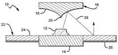
- FIG. 1is a sectional view of one embodiment of an efficient LED package according to the present invention.
- FIG. 3is a sectional view of another embodiment of an LED package according to the present invention having more than one reflector;
- FIG. 6is a sectional view of another embodiment of an LED package according to the present invention having an inverted LED and hemispheric reflector;
- FIG. 9is a flow diagram for one embodiment of a method for generating light according to the present invention.
- FIG. 10is a flow diagram for another embodiment of a method for generating light according to the present invention.
- the present inventionprovides an efficient LED package and method for efficiently emitting light from an LED package.
- the apparatus and methods according to the present inventionarrange a reflective conversion material remote to the LED. This approach allows for the down-conversion of the LED light to another wavelength using a relatively thin and dense layer of phosphor materials. This reduces the path length of the light within the converter material and improves the LED package efficiency.
- the color of LED package emissionis controlled by the composition of a reflective converter film, which can comprise both color conversion materials and neutral high reflectivity materials, or a thin phosphor layer on a uniformly coated high reflective (e.g. silver or aluminum mirror) surface possibly in combination with a binder, such as an epoxy or silicone.
- Different embodiments of the inventionincorporate an optical arrangement wherein the light from the conversion material is reflected towards the user and not back reflected towards the package.
- the LED packages according to the present inventionallow for photons emitted by the LED towards the phosphor to not significantly backscatter light towards low reflectivity, low light extraction elements within the lamp. The scattering and absorption events are thus minimized for all photons and the light extraction from the LED package occurs with a small number of passes.
- the conversion material remote to the LEDthe conversion material remains cooler further improving the lamp efficiency.
- the conversion materialcan also be pre-fabricated for LED packages according to the present invention, which allows the packages to be reproducible.
- the semiconductor light emitting devicemay be gallium nitride-based LEDs or lasers fabricated on a silicon carbide substrate such as those devices manufactured and sold by Cree, Inc. of Durham, N.C., although other emitting devices from other material systems may also be used.
- LEDstypically have an active region sandwiched between two oppositely doped layers that are either doped p-type or n-type.
- the top layer of the LEDis usually p-type and bottom layer is usually n-type, although LEDs also work if the layers are reversed.
- the p-type and n-type layershave respective contacts that each have a lead to apply a bias across p- and n-type layers. This bias results in the active layer emitting light from all surfaces of the LED.
- the LED package 10further comprises a reflector 16 mounted above the LED 12 , that can be made of any reflective material, such as a metal, or can be made of a material having one or more surfaces covered with a layer of reflective material such as silver or aluminum.
- the reflector 16is generally disc shaped and has a bottom surface 18 facing the LED 12 .
- the bottom surface 18has a hyperbolic cone shape 20 in the center with curved surfaces toward the edge of the reflector 16 . It is understood, however, that the reflector can have many different shapes and sizes and the reflector surfaces can have many different shapes to reflect the light in different directions.
- the reflector 16is arranged over the LED 12 with the bottom surface 18 facing the LED 12 with the cone 20 over the LED 12 , and in a preferred embodiment over approximately the center of the LED 12 to reflect substantially all primary LED light.
- the LED package 10also has a reflective converter 22 that is arranged remote to the LED at least partially around the LED and submount 14 .
- the reflective converteris around all of the LED and submount and as shown is mounted to the submount 14 .
- the reflective converter 22can be mounted to the LED package in many different ways and at many different locations. In one embodiment, for instance, the reflective converter can be mounted with a space between it and the LED package and at different angles.
- the reflective converter 22generally comprises a conversion material 24 mounted on a reflective element 26 .
- the conversion material 24can be mounted to reflective element 26 using many different methods such as by providing a sheet of conversion material in a binder, with the sheet being cuttable to allow portions to be affixed on the reflective element 26 .
- the conversion material 24can be formed on the reflective element 26 using electrophoretic deposition or screen printing, and then held in place by a binder, such as an epoxy. Still other methods include over-molding the phosphor conversion material on the reflective element 26 .
- the reflective converter 22can comprise conversion material 24 with neutral high reflectivity materials mixed in that gives the reflective converter its reflective properties.
- neutral high reflectivity materialscan be used, such as titanium dioxide or barium sulfate.
- the high reflective materialcan be used alone or in combination with reflective element 26 to give the reflective converter 22 its optimum reflective properties.
- the reflector 16 , LED 12 and the reflective converter 22cooperate so that at least some (and preferably most) of the light from the LED 12 reflects from the reflectors bottom surface 18 toward the reflective converter 22 .
- light along path 28is emitted from the LED 12 toward the reflector 16 , and is reflected toward the reflective converter 22 .
- the conversion material 24absorbs the light, and re-emits light in a lower frequency spectrum (down-converted) with the light emitting in a Lambertian emission pattern. Down-converted light is emitted forward from the reflective converter 22 towards the user.
- the reflector and converter geometriesare preferably designed such that the majority of the light from the reflective converter is extracted from the lamp towards the user.
- the reflector 16can reflect most of the light toward the reflective converter 22 and the reflective converter 22 can have a thickness or concentration of conversion material 24 so that some of the reflected light is down converted by the conversion material 24 , and some of the light passes through the conversion material 24 and is reflected back by the reflective element 26 . At least some of the reflected light also passes back through the conversion material without being down-converted, so that some of the LED light is reflected and emits from the reflective converter. In this embodiment, down-converted light and LED light emit back from the reflective converter with the LED package 10 emitting a wavelength combination of the down-converted and LED light.
- a preferred conversion materialcomprises one or more phosphors, and the following is a list of some of the phosphors that can be used alone or in combination as the conversion material, grouped by the re-emitted color that each emits following excitation.
- the following phosphorsare preferred for use as the conversion material based on certain desirable characteristic.
- Eachis excited in the blue and/or UV wavelength spectrum, provides a desirable peak emission, has efficient light conversion, and has acceptable Stokes shift.
- the conversion material 24can also include scattering particles to randomly refract the light as it passes through.
- the diameter of the scattering particlesshould be approximately one half of the wavelength of the light being scattered.
- Light from the LEDspass through the particles and is refracted to mix and spread the light.
- Preferred scattering particlesdo not substantially absorb LED light and have a substantially different index of refraction than the material in which it is embedded (for example, epoxy).
- the scattering particlesshould have an index of refraction higher than the material in which it is embedded.
- the LEDcan emit light in different wavelength spectrums in LED packages according to the present invention.
- the LED 12can emit light in a blue wavelength spectrum and the conversion material 24 can contain phosphors that down-converts blue light and re-emit yellow light.
- the LED package 10can then emit a white light combination of blue and yellow light.
- the conversion materialcan absorb all the blue LED light and emit a monochromatic yellow light. If a different type of phosphor is used, the package 10 can re-emit different monochromatic light, such as green.
- the LEDcan emit in the UV wavelength spectrum and the conversion material can contain different phosphors that down-convert UV light and emit different wavelengths of light that can combine to white light or other wavelengths of light.
- the phosphorscan be mixed evenly throughout the conversion material or the conversion material can have different regions where the concentration of certain phosphors can be greater. In still other embodiments, the conversion material can be divided into regions having one of the different phosphors. It is understood that at least some segments of the light path from the LED 12 to the extraction point from the lamp can include encapsulation materials like epoxies or silicones. They can be arranged continuously, or in lens or thin film form.
- FIG. 2shows another embodiment of an LED package 40 according to the present invention having an LED 42 mounted to a submount 44 , both of which are similar to the LED 12 and submount 14 shown in FIG. 1 and described above.
- the LED packagealso comprises a reflector 46 mounted over the LED 42 with the reflector made of a reflective material and arranged to reflect light from the LED as described above.
- the LED packagefurther comprises a reflective converter 52 , having a conversion material 54 similar to the conversion material 24 shown in FIG. 1 and described above.
- the conversion material 54can comprise many different materials, including one or more of the phosphors listed above.
- the conversion material 54can also comprise neutral reflective elements or scattering particles as described above.
- the reflective converter 52can also have a reflective element 56 , particularly in those embodiments not having neutral reflective elements.
- the reflective converter 52is formed in a cup around the LED 52 , submount 44 and reflector 46 combination.
- LED package 40operates in much the same way as LED package 10 in FIG. 1 , with light from the LED 42 reflected from reflector 46 to the reflective converter 52 .
- all or some of the lightcan be absorbed by the conversion material and re-emitted at a down-converted frequency spectrum.
- the LED package 40emits a wavelength combination of the LED light reflected from the reflective element 56 and the down-converted light.
- the LED package 40emits only the down-converted light.
- the LED package 40emits a wavelength combination of the down-converted light and non-reflected LED light that passes by the reflector 46 .
- the shape of the reflective converter 52provides a more directed beam of light out the opening in the reflective converter 52 . Its design together with the shape of the reflector 46 can allow for capturing essentially all light reflected by the reflector 46 onto the reflective converter 52 . Different shapes can be used for the reflective converter 52 such as hemispheric or box-shaped with an opening, with the LED 42 arranged at the base of the hemisphere or box.
- FIG. 3shows another embodiment of an LED package 70 according to the present invention having first and second LEDs 72 , 74 mounted to submount 76 , both of which are similar to the LEDs and submounts described above.
- the LED package 70further comprises first and second reflectors 78 , 80 , with the first reflector arranged over the first LED 72 and the second reflector 80 arranged over the second LED 74 .
- a single reflectorcan be arranged over the LEDs 72 , 74 .
- the LED package 70further comprises a reflective converter 82 , comprising a converter material 84 and reflective element 86 , both of which are similar to the converter materials and reflective elements above and both of which can comprise the same materials.
- the reflective converter 82is not flat, but instead has an angled portion to provide some directionality to the light emitted from the package 70 .
- light from the LEDs 72 , 74reflects from the reflectors 78 , 80 to the reflective converter 82 .
- the lightcan be fully or partially absorbed by the conversion material 84 and down-converted.
- the LED package 70emits a combination of light from the conversion material 84 and the LEDs 72 , 74 .
- the LED package 10can emit light only from the conversion material 84 or from the conversion material 84 and the LEDs 72 , 74 depending on whether the reflectors 78 , 80 reflect all or some of the light as described above.
- This embodimentprovides for the combined emission of two LEDs with the emission from the conversion material 84 .
- FIG. 4shows another embodiment of an LED package 100 according to the present invention having additional features to aid in beam shaping.
- the LED package 100comprises an LED 102 mounted to a submount 104 , although the package 100 can have more than one LED.
- a cup 106is mounted to the submount 104 , preferably around the LED 102 .
- a hemispheric lens 108is mounted to the cup 106 , over the LED 102 .
- a space 110remains between the LED 102 and the bottom of the lens 108 that is filled with a transparent or light transmitting material such as a clear epoxy or silicone.
- a reflector 112is arranged over the LED 102 with the lens arranged to focus substantially all of the LED light on the reflector 112 .
- the reflector 112can be mounted over the LED 102 using many different mounting apparatus or can be affixed to the optical element 118 .
- the cup 136is a reflective element that allows for the package 130 to be arranged without a lens.
- the reflector 138can be mounted closer to the LED 132 and the reflective converter 144 can be closer to the reflector 138 thus allowing for essentially all LED light being reflected towards the reflective converter 144 .
- the space between the LED 132 and the reflector 138is at least partially filled with encapsulation material like epoxy or silicone.
- the optical element 142has beam focusing features 146 similar to beam focusing feature 124 in FIG. 4 .
- FIG. 8shows one embodiment of a multiple LED package 190 according to the present invention comprising a circuit board 192 with multiple LEDs 194 mounted to it.
- the LEDs 194can be mounted to the circuit board 192 in many different ways, but are preferably mounted to a submount 196 that is in turn mounted to the circuit board 192 .
- the circuit board 192preferably has conductive traces that allow for a signal to be applied to the circuit board 192 and conducted to the LEDs 194 causing them to emit light.
- LED packages described abovecan be manufactured using different methods known in the art. Accordingly, the specifics of the fabrication methods have only been discussed briefly herein.
Landscapes
- Engineering & Computer Science (AREA)
- General Engineering & Computer Science (AREA)
- Physics & Mathematics (AREA)
- Microelectronics & Electronic Packaging (AREA)
- Optics & Photonics (AREA)
- Led Device Packages (AREA)
Abstract
Description
Claims (46)
Priority Applications (9)
| Application Number | Priority Date | Filing Date | Title |
|---|---|---|---|
| US11/476,520US7703945B2 (en) | 2006-06-27 | 2006-06-27 | Efficient emitting LED package and method for efficiently emitting light |
| CN2007800243425ACN101479860B (en) | 2006-06-27 | 2007-05-16 | Light emitting diode package, emitter package and method for emitting light |
| CN2012104249457ACN102938443A (en) | 2006-06-27 | 2007-05-16 | LED package, emitter package and method for emitting light |
| EP07777104.6AEP2038939B1 (en) | 2006-06-27 | 2007-05-16 | Efficient emitting led package and method for efficiently emitting light |
| PCT/US2007/011759WO2008002362A1 (en) | 2006-06-27 | 2007-05-16 | Efficient emitting led package and method for efficiently emitting light |
| KR1020097001650AKR20090026196A (en) | 2006-06-27 | 2007-05-16 | Effective light emitting LED package and method for effective light emitting |
| JP2009518116AJP2009543335A (en) | 2006-06-27 | 2007-05-16 | Efficient emitting LED package and method for efficiently emitting light |
| TW096119146ATWI434429B (en) | 2006-06-27 | 2007-05-29 | Efficient emitting led package and method for efficiently emitting light |
| US12/732,014US7963666B2 (en) | 2006-06-27 | 2010-03-25 | Efficient emitting LED package and method for efficiently emitting light |
Applications Claiming Priority (1)
| Application Number | Priority Date | Filing Date | Title |
|---|---|---|---|
| US11/476,520US7703945B2 (en) | 2006-06-27 | 2006-06-27 | Efficient emitting LED package and method for efficiently emitting light |
Related Child Applications (1)
| Application Number | Title | Priority Date | Filing Date |
|---|---|---|---|
| US12/732,014ContinuationUS7963666B2 (en) | 2006-06-27 | 2010-03-25 | Efficient emitting LED package and method for efficiently emitting light |
Publications (2)
| Publication Number | Publication Date |
|---|---|
| US20070297179A1 US20070297179A1 (en) | 2007-12-27 |
| US7703945B2true US7703945B2 (en) | 2010-04-27 |
Family
ID=38669946
Family Applications (2)
| Application Number | Title | Priority Date | Filing Date |
|---|---|---|---|
| US11/476,520Active2026-09-18US7703945B2 (en) | 2006-06-27 | 2006-06-27 | Efficient emitting LED package and method for efficiently emitting light |
| US12/732,014ActiveUS7963666B2 (en) | 2006-06-27 | 2010-03-25 | Efficient emitting LED package and method for efficiently emitting light |
Family Applications After (1)
| Application Number | Title | Priority Date | Filing Date |
|---|---|---|---|
| US12/732,014ActiveUS7963666B2 (en) | 2006-06-27 | 2010-03-25 | Efficient emitting LED package and method for efficiently emitting light |
Country Status (7)
| Country | Link |
|---|---|
| US (2) | US7703945B2 (en) |
| EP (1) | EP2038939B1 (en) |
| JP (1) | JP2009543335A (en) |
| KR (1) | KR20090026196A (en) |
| CN (2) | CN102938443A (en) |
| TW (1) | TWI434429B (en) |
| WO (1) | WO2008002362A1 (en) |
Cited By (39)
| Publication number | Priority date | Publication date | Assignee | Title |
|---|---|---|---|---|
| US20100172127A1 (en)* | 2006-11-15 | 2010-07-08 | Ecolivegreen Corp. | Indirect lighting fixture with reflectors |
| US20110026257A1 (en)* | 2008-04-03 | 2011-02-03 | Koninklijke Philips Electronics N.V. | White light-emitting device |
| US20110164397A1 (en)* | 2008-09-16 | 2011-07-07 | Osram Sylvania Inc. | Led package using phosphor containing elements and light source containing same |
| US20110317398A1 (en)* | 2010-06-29 | 2011-12-29 | Osram Gesellschaft Mit Beschraenkter Haftung | Luminous device and method for operating a luminous device |
| US8115375B1 (en)* | 2009-02-23 | 2012-02-14 | Lednovation, Inc. | Chromaticity tuned solid state lighting apparatus |
| US20130021777A1 (en)* | 2011-07-24 | 2013-01-24 | Cree, Inc. | Light fixture with coextruded components |
| US20130107573A1 (en)* | 2010-08-26 | 2013-05-02 | Nippon Electric Glass Co., Ltd. | Wavelength conversion element, light source, and backlight unit for liquid crystals |
| US20130114281A1 (en)* | 2011-11-09 | 2013-05-09 | Kia Motors Corporation | Vehicle lamp structure |
| US8441179B2 (en) | 2006-01-20 | 2013-05-14 | Cree, Inc. | Lighting devices having remote lumiphors that are excited by lumiphor-converted semiconductor excitation sources |
| US8579451B2 (en) | 2011-09-15 | 2013-11-12 | Osram Sylvania Inc. | LED lamp |
| USD696449S1 (en) | 2013-03-14 | 2013-12-24 | Lsi Industries, Inc. | Lighting |
| WO2015089516A1 (en)* | 2013-12-09 | 2015-06-18 | Cree, Inc. | Optical waveguide bodies and luminaires utilizing same |
| US9101036B2 (en) | 2010-08-20 | 2015-08-04 | Research Triangle Institute | Photoluminescent nanofiber composites, methods for fabrication, and related lighting devices |
| US9127826B2 (en) | 2013-03-14 | 2015-09-08 | Lsi Industries, Inc. | Indirect lighting luminaire |
| US20150338034A1 (en)* | 2014-05-22 | 2015-11-26 | Shin-Etsu Chemical. Co., Ltd. | Wavelength conversion member and remote phosphor type light emitting apparatus |
| US9217553B2 (en) | 2007-02-21 | 2015-12-22 | Cree, Inc. | LED lighting systems including luminescent layers on remote reflectors |
| US9228706B2 (en)* | 2014-04-23 | 2016-01-05 | Brent V. Andersen | Lighting array providing visually-captivating lighting effects |
| US20160076741A1 (en)* | 2013-04-15 | 2016-03-17 | Dow Corning Corporation | Light Emitting Assembly With Spectrum-Shifting Reflectance And Method |
| US9316368B2 (en) | 2011-04-18 | 2016-04-19 | Cree, Inc. | LED luminaire including a thin phosphor layer applied to a remote reflector |
| US9366396B2 (en) | 2013-01-30 | 2016-06-14 | Cree, Inc. | Optical waveguide and lamp including same |
| US9366799B2 (en) | 2013-03-15 | 2016-06-14 | Cree, Inc. | Optical waveguide bodies and luminaires utilizing same |
| US9388947B2 (en) | 2012-08-28 | 2016-07-12 | Cree, Inc. | Lighting device including spatially segregated lumiphor and reflector arrangement |
| US9389367B2 (en) | 2013-01-30 | 2016-07-12 | Cree, Inc. | Optical waveguide and luminaire incorporating same |
| US9441811B2 (en) | 2010-08-20 | 2016-09-13 | Research Triangle Institute | Lighting devices utilizing optical waveguides and remote light converters, and related methods |
| US9562671B2 (en) | 2010-08-20 | 2017-02-07 | Research Triangle Institute | Color-tunable lighting devices and methods of use |
| US9625638B2 (en) | 2013-03-15 | 2017-04-18 | Cree, Inc. | Optical waveguide body |
| US9651740B2 (en) | 2014-01-09 | 2017-05-16 | Cree, Inc. | Extraction film for optical waveguide and method of producing same |
| US20170256693A1 (en)* | 2014-11-19 | 2017-09-07 | Mitsubishi Chemical Corporation | Spot lighting apparatus |
| US9799804B2 (en) | 2014-10-28 | 2017-10-24 | Matrix Lighting Ltd. | Light-emitting device with near full spectrum light output |
| US9798072B2 (en) | 2013-03-15 | 2017-10-24 | Cree, Inc. | Optical element and method of forming an optical element |
| US9869450B2 (en) | 2015-02-09 | 2018-01-16 | Ecosense Lighting Inc. | Lighting systems having a truncated parabolic- or hyperbolic-conical light reflector, or a total internal reflection lens; and having another light reflector |
| US20180097037A1 (en)* | 2016-10-04 | 2018-04-05 | Vuereal Inc. | Color conversion layer integration into display substrate with high intensity light sources |
| US10209429B2 (en) | 2013-03-15 | 2019-02-19 | Cree, Inc. | Luminaire with selectable luminous intensity pattern |
| US10416377B2 (en) | 2016-05-06 | 2019-09-17 | Cree, Inc. | Luminaire with controllable light emission |
| US10707277B2 (en) | 2016-10-04 | 2020-07-07 | Vuereal Inc. | Method of integrating functional tuning materials with micro devices and structures thereof |
| US10739513B2 (en) | 2018-08-31 | 2020-08-11 | RAB Lighting Inc. | Apparatuses and methods for efficiently directing light toward and away from a mounting surface |
| US10801679B2 (en) | 2018-10-08 | 2020-10-13 | RAB Lighting Inc. | Apparatuses and methods for assembling luminaires |
| US11306897B2 (en) | 2015-02-09 | 2022-04-19 | Ecosense Lighting Inc. | Lighting systems generating partially-collimated light emissions |
| US11719882B2 (en) | 2016-05-06 | 2023-08-08 | Ideal Industries Lighting Llc | Waveguide-based light sources with dynamic beam shaping |
Families Citing this family (97)
| Publication number | Priority date | Publication date | Assignee | Title |
|---|---|---|---|---|
| US7230284B2 (en) | 2001-07-24 | 2007-06-12 | Cree, Inc. | Insulating gate AlGaN/GaN HEMT |
| US8215815B2 (en) | 2005-06-07 | 2012-07-10 | Oree, Inc. | Illumination apparatus and methods of forming the same |
| WO2006131924A2 (en) | 2005-06-07 | 2006-12-14 | Oree, Advanced Illumination Solutions Inc. | Illumination apparatus |
| US8272758B2 (en) | 2005-06-07 | 2012-09-25 | Oree, Inc. | Illumination apparatus and methods of forming the same |
| CN101351891B (en) | 2005-12-22 | 2014-11-19 | 科锐公司 | lighting device |
| US8264138B2 (en) | 2006-01-20 | 2012-09-11 | Cree, Inc. | Shifting spectral content in solid state light emitters by spatially separating lumiphor films |
| US7692263B2 (en) | 2006-11-21 | 2010-04-06 | Cree, Inc. | High voltage GaN transistors |
| CN101209243B (en) | 2006-12-29 | 2010-12-08 | 石药集团中奇制药技术(石家庄)有限公司 | Liposome medicament and preparation thereof |
| US8212290B2 (en) | 2007-03-23 | 2012-07-03 | Cree, Inc. | High temperature performance capable gallium nitride transistor |
| DE202007019100U1 (en) | 2007-09-12 | 2010-09-02 | Lumitech Produktion Und Entwicklung Gmbh | LED module, LED bulb and LED light for energy-efficient reproduction of white light |
| US7915627B2 (en) | 2007-10-17 | 2011-03-29 | Intematix Corporation | Light emitting device with phosphor wavelength conversion |
| US9461201B2 (en) | 2007-11-14 | 2016-10-04 | Cree, Inc. | Light emitting diode dielectric mirror |
| US8182128B2 (en)* | 2007-12-19 | 2012-05-22 | Oree, Inc. | Planar white illumination apparatus |
| US7907804B2 (en) | 2007-12-19 | 2011-03-15 | Oree, Inc. | Elimination of stitch artifacts in a planar illumination area |
| KR20090106299A (en)* | 2008-04-05 | 2009-10-08 | 송준오 | Group III-nitride semiconductor light emitting diode device having an ohmic contact light extracting structure layer and a method of manufacturing the same |
| WO2009134433A2 (en)* | 2008-05-02 | 2009-11-05 | Light Prescriptions Innovators, Llc | Remote-phosphor led downlight |
| US8301002B2 (en) | 2008-07-10 | 2012-10-30 | Oree, Inc. | Slim waveguide coupling apparatus and method |
| US8297786B2 (en) | 2008-07-10 | 2012-10-30 | Oree, Inc. | Slim waveguide coupling apparatus and method |
| AU2009296696B2 (en)* | 2008-09-24 | 2013-03-14 | Code 3, Inc. | Light bar |
| US8764238B2 (en)* | 2008-11-06 | 2014-07-01 | Innovations In Optics, Inc. | Light emitting diode emergency lighting module |
| DE102008061032A1 (en)* | 2008-12-08 | 2010-06-10 | Osram Opto Semiconductors Gmbh | lighting device |
| US8624527B1 (en) | 2009-03-27 | 2014-01-07 | Oree, Inc. | Independently controllable illumination device |
| US8096671B1 (en) | 2009-04-06 | 2012-01-17 | Nmera, Llc | Light emitting diode illumination system |
| US20100320904A1 (en) | 2009-05-13 | 2010-12-23 | Oree Inc. | LED-Based Replacement Lamps for Incandescent Fixtures |
| US8651692B2 (en) | 2009-06-18 | 2014-02-18 | Intematix Corporation | LED based lamp and light emitting signage |
| WO2010150202A2 (en) | 2009-06-24 | 2010-12-29 | Oree, Advanced Illumination Solutions Inc. | Illumination apparatus with high conversion efficiency and methods of forming the same |
| WO2011001329A1 (en)* | 2009-06-29 | 2011-01-06 | Koninklijke Philips Electronics N.V. | Led luminaire using louvers as a heat sink |
| US8197105B2 (en)* | 2009-08-13 | 2012-06-12 | Intematix Corporation | LED-based lamps |
| US9362459B2 (en) | 2009-09-02 | 2016-06-07 | United States Department Of Energy | High reflectivity mirrors and method for making same |
| CN102022637A (en) | 2009-09-09 | 2011-04-20 | 富士迈半导体精密工业(上海)有限公司 | Illuminating device |
| US8933644B2 (en) | 2009-09-18 | 2015-01-13 | Soraa, Inc. | LED lamps with improved quality of light |
| US9293667B2 (en) | 2010-08-19 | 2016-03-22 | Soraa, Inc. | System and method for selected pump LEDs with multiple phosphors |
| US9435493B2 (en) | 2009-10-27 | 2016-09-06 | Cree, Inc. | Hybrid reflector system for lighting device |
| EP2863117B1 (en)* | 2009-11-09 | 2016-07-13 | LG Innotek Co., Ltd. | Lighting device |
| CN102080771A (en)* | 2009-11-27 | 2011-06-01 | 富准精密工业(深圳)有限公司 | Light-emitting diode lamp |
| US8466611B2 (en) | 2009-12-14 | 2013-06-18 | Cree, Inc. | Lighting device with shaped remote phosphor |
| US20110215348A1 (en)* | 2010-02-03 | 2011-09-08 | Soraa, Inc. | Reflection Mode Package for Optical Devices Using Gallium and Nitrogen Containing Materials |
| US10147850B1 (en) | 2010-02-03 | 2018-12-04 | Soraa, Inc. | System and method for providing color light sources in proximity to predetermined wavelength conversion structures |
| US8646949B2 (en)* | 2010-03-03 | 2014-02-11 | LumenFlow Corp. | Constrained folded path resonant white light scintillator |
| US9275979B2 (en) | 2010-03-03 | 2016-03-01 | Cree, Inc. | Enhanced color rendering index emitter through phosphor separation |
| JP2011249316A (en)* | 2010-03-30 | 2011-12-08 | Mitsubishi Chemicals Corp | Light emitting device |
| DE102010014099A1 (en)* | 2010-04-07 | 2011-10-13 | Siteco Beleuchtungstechnik Gmbh | Luminaire with cover |
| US9105824B2 (en) | 2010-04-09 | 2015-08-11 | Cree, Inc. | High reflective board or substrate for LEDs |
| CN102472461B (en)* | 2010-05-19 | 2014-10-15 | 松下电器产业株式会社 | Led lamp and lighting device |
| DE102010030938A1 (en)* | 2010-07-05 | 2012-01-05 | Osram Gesellschaft mit beschränkter Haftung | Light box and method for mixing light |
| US9515229B2 (en)* | 2010-09-21 | 2016-12-06 | Cree, Inc. | Semiconductor light emitting devices with optical coatings and methods of making same |
| CN101956919A (en)* | 2010-10-11 | 2011-01-26 | 鸿富锦精密工业(深圳)有限公司 | Light emitting diode lamp |
| TWI398605B (en)* | 2010-10-14 | 2013-06-11 | Hon Hai Prec Ind Co Ltd | Led lamp |
| FI125306B (en)* | 2010-10-21 | 2015-08-31 | Rofin Sinar Laser Gmbh | Packaged fiber optic component and method of manufacture thereof |
| US9816677B2 (en)* | 2010-10-29 | 2017-11-14 | Sharp Kabushiki Kaisha | Light emitting device, vehicle headlamp, illumination device, and laser element |
| US20120113619A1 (en)* | 2010-11-04 | 2012-05-10 | Au Optronics Corporation | Light source and backlight module having the same |
| CN102062350A (en)* | 2010-11-18 | 2011-05-18 | 鸿富锦精密工业(深圳)有限公司 | Light distribution device of LED (light-emitting diode) light source |
| CN103299422B (en)* | 2010-12-29 | 2016-11-02 | 3M创新有限公司 | Remote Phosphor LED Unit with Broadband Output and Controllable Color |
| WO2012103919A1 (en)* | 2011-01-31 | 2012-08-09 | Osram Ag | Illumination device comprising phosphor element and optical system |
| US11251164B2 (en) | 2011-02-16 | 2022-02-15 | Creeled, Inc. | Multi-layer conversion material for down conversion in solid state lighting |
| US9284448B2 (en) | 2011-04-14 | 2016-03-15 | Ticona Llc | Molded reflectors for light-emitting diode assemblies |
| US9453119B2 (en) | 2011-04-14 | 2016-09-27 | Ticona Llc | Polymer composition for producing articles with light reflective properties |
| US9062198B2 (en) | 2011-04-14 | 2015-06-23 | Ticona Llc | Reflectors for light-emitting diode assemblies containing a white pigment |
| US8480254B2 (en) | 2011-04-14 | 2013-07-09 | Ticona, Llc | Molded reflective structures for light-emitting diodes |
| DE102011050450A1 (en) | 2011-05-18 | 2012-11-22 | Osram Opto Semiconductors Gmbh | Optoelectronic semiconductor chip, optoelectronic semiconductor component and method for producing an optoelectronic semiconductor component |
| JP2012244085A (en)* | 2011-05-24 | 2012-12-10 | Panasonic Corp | Lighting device |
| US10243121B2 (en) | 2011-06-24 | 2019-03-26 | Cree, Inc. | High voltage monolithic LED chip with improved reliability |
| US9728676B2 (en) | 2011-06-24 | 2017-08-08 | Cree, Inc. | High voltage monolithic LED chip |
| EP2745041B8 (en)* | 2011-09-23 | 2016-09-21 | Philips Lighting Holding B.V. | Led-based luminaire having a mixing optic |
| JP6041885B2 (en) | 2011-10-14 | 2016-12-14 | スリーエム イノベイティブ プロパティズ カンパニー | Lens assembly for remote fluorescent LED device |
| JP5715307B2 (en)* | 2011-10-26 | 2015-05-07 | コーニンクレッカ フィリップス エヌ ヴェ | Light emitting device |
| WO2013062159A1 (en)* | 2011-10-27 | 2013-05-02 | Lg Electronics Inc. | Ultra slim collimator for light emitting diode |
| US8591072B2 (en) | 2011-11-16 | 2013-11-26 | Oree, Inc. | Illumination apparatus confining light by total internal reflection and methods of forming the same |
| CN103137823B (en)* | 2011-11-24 | 2015-10-07 | 展晶科技(深圳)有限公司 | Light-emitting diode and apply the direct-light-type backlight of this light-emitting diode |
| US9187621B2 (en) | 2011-12-30 | 2015-11-17 | Ticona Llc | Reflector for light-emitting devices |
| TWM435795U (en)* | 2012-04-03 | 2012-08-11 | Inhon Internat Co Ltd | Lighting structure |
| US10347609B2 (en)* | 2012-05-04 | 2019-07-09 | Micron Technology, Inc. | Solid-state transducer assemblies with remote converter material for improved light extraction efficiency and associated systems and methods |
| WO2013173065A1 (en)* | 2012-05-17 | 2013-11-21 | 3M Innovative Properties Company | Indirect luminaire |
| TWI448648B (en)* | 2012-05-30 | 2014-08-11 | Lextar Electronics Corp | Light emitting device |
| US10077886B2 (en)* | 2012-06-01 | 2018-09-18 | 3M Innovative Properties Company | Hybrid light bulbs using combinations of remote phosphor LEDS and direct emitting LEDS |
| WO2014006501A1 (en) | 2012-07-03 | 2014-01-09 | Yosi Shani | Planar remote phosphor illumination apparatus |
| TWI469398B (en)* | 2012-07-12 | 2015-01-11 | Lextar Electronics Corp | Light emitting device |
| TWI489661B (en)* | 2012-07-18 | 2015-06-21 | Lextar Electronics Corp | Light emitting device |
| US8960969B2 (en)* | 2012-09-28 | 2015-02-24 | Lsi Corporation | Semiconductor structure with waveguide |
| TW201416623A (en)* | 2012-10-25 | 2014-05-01 | 隆達電子股份有限公司 | Lighting device |
| CN104903399B (en) | 2012-12-18 | 2017-05-31 | 提克纳有限责任公司 | For the molded reflective device of light-emitting diode component |
| JP5928611B2 (en)* | 2012-12-28 | 2016-06-01 | 信越化学工業株式会社 | Light emitting device |
| DE102013100121B4 (en) | 2013-01-08 | 2025-08-14 | OSRAM Opto Semiconductors Gesellschaft mit beschränkter Haftung | Optoelectronic semiconductor component |
| CN103090228A (en)* | 2013-01-15 | 2013-05-08 | 东莞雷笛克光学有限公司 | Composite anti-glare lighting system |
| KR102114607B1 (en)* | 2013-04-01 | 2020-05-25 | 엘지전자 주식회사 | Laser Light Source |
| USD742269S1 (en) | 2013-06-12 | 2015-11-03 | Code 3, Inc. | Dual level low-profile light bar with optional speaker |
| USD748598S1 (en) | 2013-06-12 | 2016-02-02 | Code 3, Inc. | Speaker for a light bar |
| USD742270S1 (en) | 2013-06-12 | 2015-11-03 | Code 3, Inc. | Single level low-profile light bar with optional speaker |
| TW201514424A (en)* | 2013-10-08 | 2015-04-16 | Hon Hai Prec Ind Co Ltd | Light emitting diode light source module |
| DE102014100991A1 (en)* | 2014-01-28 | 2015-07-30 | Osram Opto Semiconductors Gmbh | Light-emitting device and method for producing a light-emitting device |
| US10658546B2 (en) | 2015-01-21 | 2020-05-19 | Cree, Inc. | High efficiency LEDs and methods of manufacturing |
| CN108027125A (en)* | 2015-09-29 | 2018-05-11 | 松下知识产权经营株式会社 | Light supply apparatus and light projector device |
| WO2017192795A1 (en)* | 2016-05-05 | 2017-11-09 | Ameritech Llc | Light emitting diode replacement for a fluorescent lamp |
| TWI630344B (en)* | 2016-05-26 | 2018-07-21 | 台達電子工業股份有限公司 | Wide-angle illuminating light source |
| EP3670354B1 (en)* | 2018-12-17 | 2022-05-11 | Goodrich Lighting Systems GmbH | Lighting arrangement |
| CN110748853A (en)* | 2019-10-15 | 2020-02-04 | 深圳星标科技股份有限公司 | Split type spotlight component of pointolite and lamps and lanterns thereof |
| EP4264128A4 (en)* | 2020-12-20 | 2024-11-20 | Glint Photonics, Inc. | OPTICAL CONCEPT FOR ADJUSTABLE REFLECTIVE LUMINAIRE |
Citations (14)
| Publication number | Priority date | Publication date | Assignee | Title |
|---|---|---|---|---|
| US5813753A (en) | 1997-05-27 | 1998-09-29 | Philips Electronics North America Corporation | UV/blue led-phosphor device with efficient conversion of UV/blues light to visible light |
| US5959316A (en) | 1998-09-01 | 1999-09-28 | Hewlett-Packard Company | Multiple encapsulation of phosphor-LED devices |
| EP1198016A2 (en) | 2000-10-13 | 2002-04-17 | LumiLeds Lighting U.S., LLC | Stenciling phosphor layers on light emitting diodes |
| US20030038295A1 (en) | 2001-08-22 | 2003-02-27 | Nichia Corporation | Light emitting device with fluorescent member excited by semiconductor light emitting element |
| US6578998B2 (en)* | 2001-03-21 | 2003-06-17 | A L Lightech, Inc. | Light source arrangement |
| US6641287B2 (en)* | 2001-04-11 | 2003-11-04 | Toyoda Gosei Co., Ltd. | Reflective type light-emitting diode |
| US20040041222A1 (en) | 2002-09-04 | 2004-03-04 | Loh Ban P. | Power surface mount light emitting die package |
| WO2005055328A1 (en) | 2003-12-05 | 2005-06-16 | Mitsubishi Denki Kabushiki Kaisha | Light emitting device and illumination instrument using the same |
| WO2005078338A1 (en) | 2004-02-17 | 2005-08-25 | Kelly William M | A utility lamp |
| US20050236628A1 (en) | 2004-02-26 | 2005-10-27 | Kyocera Corporation | Light-emitting apparatus and illuminating apparatus |
| US6994453B2 (en) | 2003-03-21 | 2006-02-07 | Blanchard Randall D | Illumination device having a dichroic mirror |
| US20060034084A1 (en)* | 2004-06-28 | 2006-02-16 | Kyocera Corporation | Light-emitting apparatus and illuminating apparatus |
| US7246917B2 (en)* | 2003-08-12 | 2007-07-24 | Illumination Management Solutions, Inc. | Apparatus and method for using emitting diodes (LED) in a side-emitting device |
| US7293908B2 (en)* | 2005-10-18 | 2007-11-13 | Goldeneye, Inc. | Side emitting illumination systems incorporating light emitting diodes |
Family Cites Families (15)
| Publication number | Priority date | Publication date | Assignee | Title |
|---|---|---|---|---|
| IE56781B1 (en) | 1983-03-10 | 1991-12-18 | Moy Insulation Holdings Limite | Method and apparatus for marking an article |
| US6469322B1 (en)* | 1998-02-06 | 2002-10-22 | General Electric Company | Green emitting phosphor for use in UV light emitting diodes |
| JP3624699B2 (en)* | 1998-07-03 | 2005-03-02 | スタンレー電気株式会社 | Reflective LED lamp |
| FR2789622B1 (en)* | 1999-02-11 | 2001-06-08 | Ecia Equip Composants Ind Auto | INSTALLATION FOR MANUFACTURING THERMOPLASTIC STRUCTURAL PARTS, PARTICULARLY FOR MOTOR VEHICLES |
| DE10105802A1 (en)* | 2001-02-07 | 2002-08-08 | Patent Treuhand Ges Fuer Elektrische Gluehlampen Mbh | Semiconductor component with reflector |
| JP4172196B2 (en)* | 2002-04-05 | 2008-10-29 | 豊田合成株式会社 | Light emitting diode |
| CA2489237A1 (en)* | 2002-06-13 | 2003-12-24 | Cree, Inc. | Semiconductor emitter comprising a saturated phosphor |
| JP2005191420A (en)* | 2003-12-26 | 2005-07-14 | Stanley Electric Co Ltd | Semiconductor light emitting device having wavelength conversion layer and manufacturing method thereof |
| US7355284B2 (en)* | 2004-03-29 | 2008-04-08 | Cree, Inc. | Semiconductor light emitting devices including flexible film having therein an optical element |
| JP4592320B2 (en)* | 2004-04-12 | 2010-12-01 | 三菱電機株式会社 | Light emitting device |
| AU2005240186B2 (en) | 2004-05-05 | 2011-02-03 | Rensselaer Polytechnic Institute | High efficiency light source using solid-state emitter and down-conversion material |
| JP2006066657A (en)* | 2004-08-27 | 2006-03-09 | Kyocera Corp | Light emitting device and lighting device |
| JP2006054396A (en)* | 2004-08-16 | 2006-02-23 | Toshiba Discrete Technology Kk | Light emitting device |
| US20070045641A1 (en)* | 2005-08-23 | 2007-03-01 | Yin Chua Janet B | Light source with UV LED and UV reflector |
| US7635915B2 (en) | 2006-04-26 | 2009-12-22 | Cree Hong Kong Limited | Apparatus and method for use in mounting electronic elements |
- 2006
- 2006-06-27USUS11/476,520patent/US7703945B2/enactiveActive
- 2007
- 2007-05-16CNCN2012104249457Apatent/CN102938443A/enactivePending
- 2007-05-16EPEP07777104.6Apatent/EP2038939B1/enactiveActive
- 2007-05-16KRKR1020097001650Apatent/KR20090026196A/ennot_activeCeased
- 2007-05-16CNCN2007800243425Apatent/CN101479860B/enactiveActive
- 2007-05-16WOPCT/US2007/011759patent/WO2008002362A1/enactiveSearch and Examination
- 2007-05-16JPJP2009518116Apatent/JP2009543335A/enactivePending
- 2007-05-29TWTW096119146Apatent/TWI434429B/enactive
- 2010
- 2010-03-25USUS12/732,014patent/US7963666B2/enactiveActive
Patent Citations (15)
| Publication number | Priority date | Publication date | Assignee | Title |
|---|---|---|---|---|
| US5813753A (en) | 1997-05-27 | 1998-09-29 | Philips Electronics North America Corporation | UV/blue led-phosphor device with efficient conversion of UV/blues light to visible light |
| US5959316A (en) | 1998-09-01 | 1999-09-28 | Hewlett-Packard Company | Multiple encapsulation of phosphor-LED devices |
| EP1198016A2 (en) | 2000-10-13 | 2002-04-17 | LumiLeds Lighting U.S., LLC | Stenciling phosphor layers on light emitting diodes |
| US6578998B2 (en)* | 2001-03-21 | 2003-06-17 | A L Lightech, Inc. | Light source arrangement |
| US6641287B2 (en)* | 2001-04-11 | 2003-11-04 | Toyoda Gosei Co., Ltd. | Reflective type light-emitting diode |
| US6737681B2 (en)* | 2001-08-22 | 2004-05-18 | Nichia Corporation | Light emitting device with fluorescent member excited by semiconductor light emitting element |
| US20030038295A1 (en) | 2001-08-22 | 2003-02-27 | Nichia Corporation | Light emitting device with fluorescent member excited by semiconductor light emitting element |
| US20040041222A1 (en) | 2002-09-04 | 2004-03-04 | Loh Ban P. | Power surface mount light emitting die package |
| US6994453B2 (en) | 2003-03-21 | 2006-02-07 | Blanchard Randall D | Illumination device having a dichroic mirror |
| US7246917B2 (en)* | 2003-08-12 | 2007-07-24 | Illumination Management Solutions, Inc. | Apparatus and method for using emitting diodes (LED) in a side-emitting device |
| WO2005055328A1 (en) | 2003-12-05 | 2005-06-16 | Mitsubishi Denki Kabushiki Kaisha | Light emitting device and illumination instrument using the same |
| WO2005078338A1 (en) | 2004-02-17 | 2005-08-25 | Kelly William M | A utility lamp |
| US20050236628A1 (en) | 2004-02-26 | 2005-10-27 | Kyocera Corporation | Light-emitting apparatus and illuminating apparatus |
| US20060034084A1 (en)* | 2004-06-28 | 2006-02-16 | Kyocera Corporation | Light-emitting apparatus and illuminating apparatus |
| US7293908B2 (en)* | 2005-10-18 | 2007-11-13 | Goldeneye, Inc. | Side emitting illumination systems incorporating light emitting diodes |
Non-Patent Citations (3)
| Title |
|---|
| Nichia Corp. White LED, Part No. NSPW300BS, "Specifications for Nichia White LED Model NSPW300BS", pp. 1-14, 2004. |
| Nichia Corp. White LED, Part No. NSPW312BX, "Specifications for Nichia White LED, Model NSW312BS", pp. 1-14, 2004. |
| PCT Search Report Nov. 20, 2007, Written Opinion. |
Cited By (60)
| Publication number | Priority date | Publication date | Assignee | Title |
|---|---|---|---|---|
| US9220149B2 (en) | 2006-01-20 | 2015-12-22 | Cree, Inc. | Lighting devices having remote lumiphors that are excited by lumiphor-converted semiconductor excitation sources |
| US8441179B2 (en) | 2006-01-20 | 2013-05-14 | Cree, Inc. | Lighting devices having remote lumiphors that are excited by lumiphor-converted semiconductor excitation sources |
| US20100172127A1 (en)* | 2006-11-15 | 2010-07-08 | Ecolivegreen Corp. | Indirect lighting fixture with reflectors |
| US9217553B2 (en) | 2007-02-21 | 2015-12-22 | Cree, Inc. | LED lighting systems including luminescent layers on remote reflectors |
| US20110026257A1 (en)* | 2008-04-03 | 2011-02-03 | Koninklijke Philips Electronics N.V. | White light-emitting device |
| US8348458B2 (en)* | 2008-04-03 | 2013-01-08 | Koninklijke Philips Electronics N.V. | White light-emitting device |
| US20110164397A1 (en)* | 2008-09-16 | 2011-07-07 | Osram Sylvania Inc. | Led package using phosphor containing elements and light source containing same |
| US8525207B2 (en) | 2008-09-16 | 2013-09-03 | Osram Sylvania Inc. | LED package using phosphor containing elements and light source containing same |
| US8115375B1 (en)* | 2009-02-23 | 2012-02-14 | Lednovation, Inc. | Chromaticity tuned solid state lighting apparatus |
| US8974087B2 (en)* | 2010-06-29 | 2015-03-10 | Osram Gesellschaft Mit Beschraenkter Haftung | Luminous device and method for operating a luminous device |
| US20110317398A1 (en)* | 2010-06-29 | 2011-12-29 | Osram Gesellschaft Mit Beschraenkter Haftung | Luminous device and method for operating a luminous device |
| US9562671B2 (en) | 2010-08-20 | 2017-02-07 | Research Triangle Institute | Color-tunable lighting devices and methods of use |
| US9101036B2 (en) | 2010-08-20 | 2015-08-04 | Research Triangle Institute | Photoluminescent nanofiber composites, methods for fabrication, and related lighting devices |
| US9441811B2 (en) | 2010-08-20 | 2016-09-13 | Research Triangle Institute | Lighting devices utilizing optical waveguides and remote light converters, and related methods |
| US20130107573A1 (en)* | 2010-08-26 | 2013-05-02 | Nippon Electric Glass Co., Ltd. | Wavelength conversion element, light source, and backlight unit for liquid crystals |
| US9316368B2 (en) | 2011-04-18 | 2016-04-19 | Cree, Inc. | LED luminaire including a thin phosphor layer applied to a remote reflector |
| US9534765B2 (en)* | 2011-07-24 | 2017-01-03 | Cree, Inc. | Light fixture with coextruded components |
| US20130021777A1 (en)* | 2011-07-24 | 2013-01-24 | Cree, Inc. | Light fixture with coextruded components |
| US8579451B2 (en) | 2011-09-15 | 2013-11-12 | Osram Sylvania Inc. | LED lamp |
| US20130114281A1 (en)* | 2011-11-09 | 2013-05-09 | Kia Motors Corporation | Vehicle lamp structure |
| US9388947B2 (en) | 2012-08-28 | 2016-07-12 | Cree, Inc. | Lighting device including spatially segregated lumiphor and reflector arrangement |
| US9366396B2 (en) | 2013-01-30 | 2016-06-14 | Cree, Inc. | Optical waveguide and lamp including same |
| US9581751B2 (en) | 2013-01-30 | 2017-02-28 | Cree, Inc. | Optical waveguide and lamp including same |
| US10436969B2 (en) | 2013-01-30 | 2019-10-08 | Ideal Industries Lighting Llc | Optical waveguide and luminaire incorporating same |
| US9389367B2 (en) | 2013-01-30 | 2016-07-12 | Cree, Inc. | Optical waveguide and luminaire incorporating same |
| USD696449S1 (en) | 2013-03-14 | 2013-12-24 | Lsi Industries, Inc. | Lighting |
| USD707873S1 (en) | 2013-03-14 | 2014-06-24 | Lsi Industries, Inc. | Lighting |
| USD739977S1 (en) | 2013-03-14 | 2015-09-29 | Lsi Industries, Inc. | Lighting |
| US9127826B2 (en) | 2013-03-14 | 2015-09-08 | Lsi Industries, Inc. | Indirect lighting luminaire |
| US9625638B2 (en) | 2013-03-15 | 2017-04-18 | Cree, Inc. | Optical waveguide body |
| US9366799B2 (en) | 2013-03-15 | 2016-06-14 | Cree, Inc. | Optical waveguide bodies and luminaires utilizing same |
| US10209429B2 (en) | 2013-03-15 | 2019-02-19 | Cree, Inc. | Luminaire with selectable luminous intensity pattern |
| US9798072B2 (en) | 2013-03-15 | 2017-10-24 | Cree, Inc. | Optical element and method of forming an optical element |
| US20160076741A1 (en)* | 2013-04-15 | 2016-03-17 | Dow Corning Corporation | Light Emitting Assembly With Spectrum-Shifting Reflectance And Method |
| US9726351B2 (en)* | 2013-04-15 | 2017-08-08 | Dow Corning Corporation | Light emitting assembly with spectrum-shifting reflectance and method |
| WO2015089516A1 (en)* | 2013-12-09 | 2015-06-18 | Cree, Inc. | Optical waveguide bodies and luminaires utilizing same |
| US9651740B2 (en) | 2014-01-09 | 2017-05-16 | Cree, Inc. | Extraction film for optical waveguide and method of producing same |
| US9228706B2 (en)* | 2014-04-23 | 2016-01-05 | Brent V. Andersen | Lighting array providing visually-captivating lighting effects |
| US20150338034A1 (en)* | 2014-05-22 | 2015-11-26 | Shin-Etsu Chemical. Co., Ltd. | Wavelength conversion member and remote phosphor type light emitting apparatus |
| US9799804B2 (en) | 2014-10-28 | 2017-10-24 | Matrix Lighting Ltd. | Light-emitting device with near full spectrum light output |
| US20170256693A1 (en)* | 2014-11-19 | 2017-09-07 | Mitsubishi Chemical Corporation | Spot lighting apparatus |
| US10361348B2 (en)* | 2014-11-19 | 2019-07-23 | Mitsubishi Chemical Corporation | Spot lighting apparatus |
| US9869450B2 (en) | 2015-02-09 | 2018-01-16 | Ecosense Lighting Inc. | Lighting systems having a truncated parabolic- or hyperbolic-conical light reflector, or a total internal reflection lens; and having another light reflector |
| US11614217B2 (en) | 2015-02-09 | 2023-03-28 | Korrus, Inc. | Lighting systems generating partially-collimated light emissions |
| US11306897B2 (en) | 2015-02-09 | 2022-04-19 | Ecosense Lighting Inc. | Lighting systems generating partially-collimated light emissions |
| US11372156B2 (en) | 2016-05-06 | 2022-06-28 | Ideal Industries Lighting Llc | Waveguide-based light sources with dynamic beam shaping |
| US10416377B2 (en) | 2016-05-06 | 2019-09-17 | Cree, Inc. | Luminaire with controllable light emission |
| US12353005B2 (en) | 2016-05-06 | 2025-07-08 | Cree Lighting Usa Llc | Waveguide-based light sources with dynamic beam shaping |
| US11719882B2 (en) | 2016-05-06 | 2023-08-08 | Ideal Industries Lighting Llc | Waveguide-based light sources with dynamic beam shaping |
| US10527785B2 (en) | 2016-05-06 | 2020-01-07 | Ideal Industries Lighting Llc | Waveguide-based light sources with dynamic beam shaping |
| US10890714B2 (en) | 2016-05-06 | 2021-01-12 | Ideal Industries Lighting Llc | Waveguide-based light sources with dynamic beam shaping |
| US10312296B2 (en)* | 2016-10-04 | 2019-06-04 | Vuereal Inc. | Color conversion layer integration into display substrate with high intensity light sources |
| US11322556B2 (en) | 2016-10-04 | 2022-05-03 | Vue Real Inc. | Method of integrating functional tuning materials with micro devices and structures thereof |
| US20180097037A1 (en)* | 2016-10-04 | 2018-04-05 | Vuereal Inc. | Color conversion layer integration into display substrate with high intensity light sources |
| US11581373B2 (en) | 2016-10-04 | 2023-02-14 | Vuereal Inc. | Method of integrating functional tuning materials with micro devices and structures thereof |
| US11985883B2 (en) | 2016-10-04 | 2024-05-14 | Vuereal Inc. | Method of integrating functional tuning materials with micro devices and structures thereof |
| US10707277B2 (en) | 2016-10-04 | 2020-07-07 | Vuereal Inc. | Method of integrating functional tuning materials with micro devices and structures thereof |
| US12436415B2 (en) | 2016-10-04 | 2025-10-07 | Vuereal Inc. | Method of integrating functional tuning materials with micro devices and structures thereof |
| US10739513B2 (en) | 2018-08-31 | 2020-08-11 | RAB Lighting Inc. | Apparatuses and methods for efficiently directing light toward and away from a mounting surface |
| US10801679B2 (en) | 2018-10-08 | 2020-10-13 | RAB Lighting Inc. | Apparatuses and methods for assembling luminaires |
Also Published As
| Publication number | Publication date |
|---|---|
| EP2038939A1 (en) | 2009-03-25 |
| EP2038939B1 (en) | 2016-07-13 |
| TWI434429B (en) | 2014-04-11 |
| US7963666B2 (en) | 2011-06-21 |
| CN101479860B (en) | 2012-12-19 |
| KR20090026196A (en) | 2009-03-11 |
| US20100177497A1 (en) | 2010-07-15 |
| US20070297179A1 (en) | 2007-12-27 |
| JP2009543335A (en) | 2009-12-03 |
| CN101479860A (en) | 2009-07-08 |
| CN102938443A (en) | 2013-02-20 |
| TW200805717A (en) | 2008-01-16 |
| WO2008002362A1 (en) | 2008-01-03 |
Similar Documents
| Publication | Publication Date | Title |
|---|---|---|
| US7703945B2 (en) | Efficient emitting LED package and method for efficiently emitting light | |
| US7005679B2 (en) | Multiple component solid state white light | |
| US8169135B2 (en) | Semiconductor lighting device with wavelength conversion on back-transferred light path | |
| US9220149B2 (en) | Lighting devices having remote lumiphors that are excited by lumiphor-converted semiconductor excitation sources | |
| EP1512181B1 (en) | Semiconductor emitter comprising a saturated phosphor | |
| US8740413B1 (en) | System and method for providing color light sources in proximity to predetermined wavelength conversion structures | |
| US20140225137A1 (en) | System and method for providing color light sources in proximity to predetermined wavelength conversion structures | |
| US8801218B2 (en) | Lighting device capable of emitting light with a wide angle | |
| KR20170069240A (en) | Light source with tunable emission spectrum | |
| JP5374332B2 (en) | Lighting device | |
| JP2006210627A (en) | Light emitting element storage package, light emitting device, and lighting device | |
| KR20130016940A (en) | Lighting device | |
| US10125947B2 (en) | Board and light source module including the same | |
| JP7027161B2 (en) | Lighting equipment and lighting modules | |
| JP7042683B2 (en) | Lighting equipment | |
| JP7274013B2 (en) | lighting devices and lighting modules | |
| JP2005294796A (en) | Light emitting element storage package, light emitting device, and lighting device |
Legal Events
| Date | Code | Title | Description |
|---|---|---|---|
| AS | Assignment | Owner name:CREE, INC., CALIFORNIA Free format text:ASSIGNMENT OF ASSIGNORS INTEREST;ASSIGNORS:LEUNG, MICHAEL;KELLER, BERND;IBBETSON, JAMES;AND OTHERS;REEL/FRAME:018023/0820 Effective date:20060615 Owner name:CREE, INC.,CALIFORNIA Free format text:ASSIGNMENT OF ASSIGNORS INTEREST;ASSIGNORS:LEUNG, MICHAEL;KELLER, BERND;IBBETSON, JAMES;AND OTHERS;REEL/FRAME:018023/0820 Effective date:20060615 | |
| STCF | Information on status: patent grant | Free format text:PATENTED CASE | |
| FPAY | Fee payment | Year of fee payment:4 | |
| MAFP | Maintenance fee payment | Free format text:PAYMENT OF MAINTENANCE FEE, 8TH YEAR, LARGE ENTITY (ORIGINAL EVENT CODE: M1552) Year of fee payment:8 | |
| AS | Assignment | Owner name:CREELED, INC., NORTH CAROLINA Free format text:ASSIGNMENT OF ASSIGNORS INTEREST;ASSIGNOR:CREE, INC.;REEL/FRAME:057017/0311 Effective date:20210301 | |
| MAFP | Maintenance fee payment | Free format text:PAYMENT OF MAINTENANCE FEE, 12TH YEAR, LARGE ENTITY (ORIGINAL EVENT CODE: M1553); ENTITY STATUS OF PATENT OWNER: LARGE ENTITY Year of fee payment:12 | |
| AS | Assignment | Owner name:CITIZENS BANK, N.A., MASSACHUSETTS Free format text:SECURITY INTEREST;ASSIGNORS:SMART MODULAR TECHNOLOGIES, INC.;SMART HIGH RELIABILITY SOLUTIONS, LLC;SMART EMBEDDED COMPUTING, INC.;AND OTHERS;REEL/FRAME:058983/0001 Effective date:20220207 | |
| AS | Assignment | Owner name:SMART MODULAR TECHNOLOGIES, INC., CALIFORNIA Free format text:RELEASE OF PATENT SECURITY INTEREST RECORDED AT R/F 058983/0001;ASSIGNOR:CITIZENS BANK, N.A.;REEL/FRAME:071725/0207 Effective date:20250624 Owner name:SMART EMBEDDED COMPUTING, INC., ARIZONA Free format text:RELEASE OF PATENT SECURITY INTEREST RECORDED AT R/F 058983/0001;ASSIGNOR:CITIZENS BANK, N.A.;REEL/FRAME:071725/0207 Effective date:20250624 Owner name:SMART HIGH RELIABILITY SOLUTIONS LLC, CALIFORNIA Free format text:RELEASE OF PATENT SECURITY INTEREST RECORDED AT R/F 058983/0001;ASSIGNOR:CITIZENS BANK, N.A.;REEL/FRAME:071725/0207 Effective date:20250624 Owner name:CREELED, INC., CALIFORNIA Free format text:RELEASE OF PATENT SECURITY INTEREST RECORDED AT R/F 058983/0001;ASSIGNOR:CITIZENS BANK, N.A.;REEL/FRAME:071725/0207 Effective date:20250624 | |
| AS | Assignment | Owner name:JPMORGAN CHASE BANK, N.A., ILLINOIS Free format text:PATENT SECURITY AGREEMENT;ASSIGNORS:CREELED, INC.;PENGUIN SOLUTIONS CORPORATION (DE);SMART EMBEDDED COMPUTING, INC.;AND OTHERS;REEL/FRAME:071755/0001 Effective date:20250624 |