US7702831B2 - Flash memory controller for electronic data flash card - Google Patents
Flash memory controller for electronic data flash cardDownload PDFInfo
- Publication number
- US7702831B2 US7702831B2US11/466,759US46675906AUS7702831B2US 7702831 B2US7702831 B2US 7702831B2US 46675906 AUS46675906 AUS 46675906AUS 7702831 B2US7702831 B2US 7702831B2
- Authority
- US
- United States
- Prior art keywords
- flash memory
- data
- mbc
- memory device
- memory controller
- Prior art date
- Legal status (The legal status is an assumption and is not a legal conclusion. Google has not performed a legal analysis and makes no representation as to the accuracy of the status listed.)
- Expired - Fee Related, expires
Links
Images


Classifications
- G—PHYSICS
- G06—COMPUTING OR CALCULATING; COUNTING
- G06F—ELECTRIC DIGITAL DATA PROCESSING
- G06F12/00—Accessing, addressing or allocating within memory systems or architectures
- G06F12/02—Addressing or allocation; Relocation
- G06F12/0223—User address space allocation, e.g. contiguous or non contiguous base addressing
- G06F12/023—Free address space management
- G06F12/0238—Memory management in non-volatile memory, e.g. resistive RAM or ferroelectric memory
- G06F12/0246—Memory management in non-volatile memory, e.g. resistive RAM or ferroelectric memory in block erasable memory, e.g. flash memory
- G—PHYSICS
- G06—COMPUTING OR CALCULATING; COUNTING
- G06F—ELECTRIC DIGITAL DATA PROCESSING
- G06F12/00—Accessing, addressing or allocating within memory systems or architectures
- G06F12/14—Protection against unauthorised use of memory or access to memory
- G06F12/1416—Protection against unauthorised use of memory or access to memory by checking the object accessibility, e.g. type of access defined by the memory independently of subject rights
- G—PHYSICS
- G06—COMPUTING OR CALCULATING; COUNTING
- G06F—ELECTRIC DIGITAL DATA PROCESSING
- G06F21/00—Security arrangements for protecting computers, components thereof, programs or data against unauthorised activity
- G06F21/30—Authentication, i.e. establishing the identity or authorisation of security principals
- G06F21/31—User authentication
- G06F21/32—User authentication using biometric data, e.g. fingerprints, iris scans or voiceprints
- G—PHYSICS
- G06—COMPUTING OR CALCULATING; COUNTING
- G06F—ELECTRIC DIGITAL DATA PROCESSING
- G06F21/00—Security arrangements for protecting computers, components thereof, programs or data against unauthorised activity
- G06F21/70—Protecting specific internal or peripheral components, in which the protection of a component leads to protection of the entire computer
- G06F21/78—Protecting specific internal or peripheral components, in which the protection of a component leads to protection of the entire computer to assure secure storage of data
- G06F21/79—Protecting specific internal or peripheral components, in which the protection of a component leads to protection of the entire computer to assure secure storage of data in semiconductor storage media, e.g. directly-addressable memories
- G—PHYSICS
- G06—COMPUTING OR CALCULATING; COUNTING
- G06K—GRAPHICAL DATA READING; PRESENTATION OF DATA; RECORD CARRIERS; HANDLING RECORD CARRIERS
- G06K19/00—Record carriers for use with machines and with at least a part designed to carry digital markings
- G06K19/06—Record carriers for use with machines and with at least a part designed to carry digital markings characterised by the kind of the digital marking, e.g. shape, nature, code
- G06K19/067—Record carriers with conductive marks, printed circuits or semiconductor circuit elements, e.g. credit or identity cards also with resonating or responding marks without active components
- G06K19/07—Record carriers with conductive marks, printed circuits or semiconductor circuit elements, e.g. credit or identity cards also with resonating or responding marks without active components with integrated circuit chips
- G06K19/073—Special arrangements for circuits, e.g. for protecting identification code in memory
- G06K19/07309—Means for preventing undesired reading or writing from or onto record carriers
- G06K19/07345—Means for preventing undesired reading or writing from or onto record carriers by activating or deactivating at least a part of the circuit on the record carrier, e.g. ON/OFF switches
- G06K19/07354—Means for preventing undesired reading or writing from or onto record carriers by activating or deactivating at least a part of the circuit on the record carrier, e.g. ON/OFF switches by biometrically sensitive means, e.g. fingerprint sensitive
- G—PHYSICS
- G06—COMPUTING OR CALCULATING; COUNTING
- G06V—IMAGE OR VIDEO RECOGNITION OR UNDERSTANDING
- G06V40/00—Recognition of biometric, human-related or animal-related patterns in image or video data
- G06V40/10—Human or animal bodies, e.g. vehicle occupants or pedestrians; Body parts, e.g. hands
- G06V40/12—Fingerprints or palmprints
- G06V40/1365—Matching; Classification
- G—PHYSICS
- G07—CHECKING-DEVICES
- G07C—TIME OR ATTENDANCE REGISTERS; REGISTERING OR INDICATING THE WORKING OF MACHINES; GENERATING RANDOM NUMBERS; VOTING OR LOTTERY APPARATUS; ARRANGEMENTS, SYSTEMS OR APPARATUS FOR CHECKING NOT PROVIDED FOR ELSEWHERE
- G07C9/00—Individual registration on entry or exit
- G07C9/20—Individual registration on entry or exit involving the use of a pass
- G07C9/22—Individual registration on entry or exit involving the use of a pass in combination with an identity check of the pass holder
- G07C9/25—Individual registration on entry or exit involving the use of a pass in combination with an identity check of the pass holder using biometric data, e.g. fingerprints, iris scans or voice recognition
- G07C9/257—Individual registration on entry or exit involving the use of a pass in combination with an identity check of the pass holder using biometric data, e.g. fingerprints, iris scans or voice recognition electronically
Definitions
- the inventionrelates to electronic data flash cards, more particularly to a system and method for controlling flash memory in an electronic data flash card.
- Confidential data filesare often stored in floppy disks or are delivered via networks that require passwords or that use encryption coding for security. Confidential documents are sent by adding safety seals and impressions during delivery. However, confidential data files and documents are exposed to the danger that the passwords, encryption codes, safety seals and impressions may be broken (deciphered), thereby resulting in unauthorized access to the confidential information.
- Flash memoryAs flash memory technology becomes more advanced, flash memory is replacing traditional magnetic disks as storage media for mobile systems. Flash memory has significant advantages over floppy disks or magnetic hard disks such as having high-G resistance and low power dissipation. Because of the smaller physical size of flash memory, they are also more conducive to mobile systems. Accordingly, the flash memory trend has been growing because of its compatibility with mobile systems and low-power feature. However, advances in flash technology have created a greater variety of flash memory device types that vary for reasons of performance, cost and capacity. As such, a problem arises when mobile systems that are designed for one type of flash memory are constructed using another, incompatible type of flash memory.
- PCpersonal computer
- USBUniversal Serial Bus
- flash memoryis also replacing floppy disks because flash memory provides higher storage capacity and faster access speeds than floppy drives.
- USB standardhas several features that require additional processing resources. These features include fixed-frame times, transaction packets, and enumeration processes. For better optimization, these features have been implemented in application-specific integrated circuits (ASICs).
- ASICsapplication-specific integrated circuits
- USB mass-storage devicesare slow.
- the USB interfaceis significantly slower than IDE (Integrated Drive Electronics) interface in particular. This is because of the overhead associated with the USB standard, which include additional resources required for managing USB commands and handshake packets. Bulk-only transactions introduced by the USB standard have relieved some resources but only if the USB traffic is not too busy.
- flash memory sectorsthat have already been programmed must be erased before being reprogrammed. Also, flash memory sectors have a limited life span; i.e., they can be erased only a limited number of times before failure. Accordingly, flash memory access is slow due to the erase-before-write nature and ongoing erasing will damage the flash memory sectors over time.
- USB-standard flash memoryTo address the speed problems with USB-standard flash memory, hardware and firmware utilize existing small computer systems interface (SCSI) protocols so that flash memory can function as mass-storage devices similarly to magnetic hard disks. SCSI protocols have been used in USB-standard mass-storage devices long before flash memory devices have been widely adopted as storage media. Accordingly, the USB standard has incorporated traditional SCSI protocols to manage flash memory.
- SCSIsmall computer systems interface
- a problem with SCSI protocolsis that they do not include an erase command to address the erase-before-write nature of flash memory. Accordingly, the erase operation is handled by the host system, which further ties up the host system resources.
- USB packet definitionssuch as write flash, read flash, and erase flash definitions.
- write flashread flash
- erase flash definitionsare not an efficient way to handle flash memory because they introduce additional protocols that require additional computing resources at the host system. They also do not address the sector-wear issues.
- Another solutionprovides a driver procedure for flash memory write transactions.
- This procedurehas three different sub-procedures. Generally, the data of a requested flash memory address is first read. If there is data already written to that address, the firmware executes an erase command. Then, if the erase command executes correctly, the firmware executes a write request.
- this driver procedureutilizes protocols that require additional computing resources at the host system.
- Another solutionprovides a flash sector format that has two fields: a data field and a spare field.
- the spare fieldcontains control data that include flags that facilitate in the management of the sectors.
- the flagsintroduce ASIC complexity when the host system writes to the sectors.
- an electronic data flash cardthat includes an intelligent processing unit for flexible flash memory type support.
- the system and methodshould be able to comply with the USB standard, should be suitable for ASIC hardware implementation, and should be simple, cost effective and capable of being easily adapted to existing technology.
- the present inventionis generally directed to an electronic data flash card including a flash memory device, a fingerprint sensor, an input-output interface circuit and a processing unit.
- the electronic data flash cardis adapted to be accessed by a host (external) computer such as a personal computer, notebook computer or other electronic host device.
- a hostexternal
- personal datacan be stored inside the flash memory device in an encrypted form such that it can only be accessed, for example, by way of a fingerprint sensor associated with card body to make sure unauthorized person cannot misuse the card.
- a flash memory controlleris part of the processing unit to control the operation of the flash memory device.
- the processing unitis connected to the flash memory device and the input/output interface circuit.
- the flash memory controller logicincludes a flash type algorithm for detecting whether the flash memory device is of a flash type that is supported by the flash memory controller logic.
- the processing unit of an electronic data flash cardis operable selectively in a programming mode, a data retrieving mode, and a resetting mode.
- the processing unitWhen the processing unit is in the programming mode, the processing unit activates the input/output interface circuit to receive the confidential data file from the host computer, and to store the data file in the flash memory device.
- the processing unitWhen the processing unit is in the data retrieving mode, the processing unit activates the input/output interface circuit to transmit the data file to the host computer.
- the data resetting modethe data file (and the reference fingerprint data) is/are erased from the flash memory device.
- the processing unitis a microprocessor including one of an 8051, 8052, 80286, RISC, ARM, MIPS or digital signal processor.
- the input/output (I/O) interface circuitis a USB interface circuit.
- a USB flash devicetransfers high-speed data between computers using only the Bulk-Only Transfer (BOT) protocol.
- BOTis a more efficient and faster transfer protocol than command/bulk/interrupt (CBI) protocol because BOT transport of command, data, status rely on Bulk endpoints in addition to default Control endpoints.
- CBIcommand/bulk/interrupt
- the flash memory controllerincludes a processor for receiving at least one request from a host system.
- the flash memory controllerfurther includes an index including information regarding sectors of a flash memory.
- the processorutilizes the index to determine the sectors of the flash memory that are available for programming, reprogramming, or reading.
- the flash memory controllerfurther includes a first-in-first-out unit (FIFO) for recycling obsolete sectors so that they are available for reprogramming.
- FIFOfirst-in-first-out unit
- the host systeminteracts with the flash memory controller without the host system having information regarding the configuration of the flash memory. Consequently, speeds at which data is written to and read from flash memory is significantly increased while the flash memory remains compatible with the USB standard and ASIC architecture.
- FIG. 1is a block diagram showing an electronic data flash card with fingerprint verification capability in accordance with an embodiment of the present invention.
- FIG. 2is a schematic circuit block diagram illustrating an electronic data flash card according to another embodiment of the present invention.
- FIG. 3is a block diagram of a processing unit utilized in an electronic data flash card in accordance with another embodiment of the present invention.
- FIG. 4Ais a flow chart showing a process for detecting a flash memory type in accordance with an embodiment of the present invention.
- FIG. 4Bis a block diagram showing a portion of an electronic data flash card according to another embodiment of the present invention.
- FIG. 5Ais a block diagram illustrating an 8-bit access with 8-bit data flash memory.
- FIG. 5Bis a block diagram illustrating a 16-bit access with 16-bit data flash memory.
- FIG. 5Cis a block diagram illustrating a 16-bit dual channel access with two 8-bit data flash memories via a single control.
- FIG. 5Dis a block diagram illustrating a 16-bit interleave channel access with two 8-bit data flash memories via separate controls according to an embodiment of the present invention.
- FIG. 6is a schematic circuit block diagram illustrating an electronic data flash card according to another embodiment of the present invention.
- FIG. 7is a block diagram of a flash memory system including a flash memory controller and a flash memory in accordance with the present invention.
- FIG. 8is a block diagram showing in more detail the write look-up table, the read look-up table, the physical usage table, and the recycling first-in-first-out unit of FIG. 7 in accordance with the present invention.
- FIG. 9is a block diagram showing in more detail the flash memory of FIG. 7 in accordance with the present invention.
- FIG. 10is a high-level flow chart showing a method for managing flash memory in accordance with the present invention.
- FIG. 11is a flow chart showing a method for transmitting USB mass-storage class service requests in accordance with the present invention.
- FIGS. 12A , 12 B and 12 Care block diagrams showing a command block wrapper, a reduced block command read format, and a command status wrapper in accordance with the present invention.
- FIG. 13is a flow chart showing a method for reading, writing, and erasing in accordance with the present invention.
- FIG. 14is a high-level flow chart showing a method including a first phase of a write transaction, a second phase of the write transaction, a read transaction, and a recycling operation in accordance with the present invention.
- FIGS. 15A , 15 B, 15 C and 15 Dare block diagrams illustrating exemplary results from first and second phases of a write transaction in accordance with the present invention.
- FIG. 16is a flow chart showing a method for implementing the first phase of the write transaction of FIG. 14 in accordance with the present invention.
- FIG. 17is a flow chart showing a method for implementing the second phase of the write transaction of FIG. 14 in accordance with the present invention.
- FIG. 18is a flow chart showing a method for implementing the read transaction of FIG. 14 in accordance with the present invention.
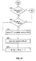
- FIG. 19is a flow chart showing a method for implementing the recycling operation of FIG. 14 in accordance with the present invention.
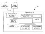
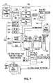
- an electronic data flash card 10is adapted to be accessed by an external (host) computer 9 either via an interface bus 13 or a card reader 12 or other interface mechanism (not shown), and includes a card body 1 , a processing unit 2 , one or more flash memory devices 3 , a fingerprint sensor 4 , an input/output interface circuit 5 , an optional display unit 6 , an optional power source (e.g., battery) 7 , and an optional function key set 8 .
- an external (host) computer 9either via an interface bus 13 or a card reader 12 or other interface mechanism (not shown)
- a card body 1includes a card body 1 , a processing unit 2 , one or more flash memory devices 3 , a fingerprint sensor 4 , an input/output interface circuit 5 , an optional display unit 6 , an optional power source (e.g., battery) 7 , and an optional function key set 8 .
- an optional power sourcee.g., battery
- Flash memory device 3is mounted on the card body 1 , stores in a known manner therein one or more data files, a reference password, and the reference fingerprint data obtained by scanning a fingerprint of one or more authorized users of the electronic data flash card 10 . Only authorized users can access the stored data files.
- the data filecan be a picture file or a text file.
- the fingerprint sensor 4is mounted on the card body 1 , and is adapted to scan a fingerprint of a user of electronic data flash card 10 to generate fingerprint scan data.
- One example of the fingerprint sensor 4 that can be used in the present inventionis that disclosed in a co-owned U.S. Pat. No. 6,547,130, entitled “INTEGRATED CIRCUIT CARD WITH FINGERPRINT VERIFICATION CAPABILITY”, the entire disclosure of which is incorporated herein by reference.
- the fingerprint sensor described in the above patentincludes an array of scan cells that defines a fingerprint scanning area.
- the fingerprint scan dataincludes a plurality of scan line data obtained by scanning corresponding lines of array of scan cells.
- the lines of array of scan cellsare scanned in a row direction as well as column direction of said array.
- Each of the scan cellsgenerates a first logic signal upon detection of a ridge in the fingerprint of the holder of card body, and a second logic signal upon detection of a valley in the fingerprint of the holder of card body.
- the input/output interface circuit 5is mounted on the card body 1 , and can be activated so as to establish communication with the host computer 9 by way of an appropriate socket via an interface bus 13 or a card reader 12 .
- input/output interface circuit 5includes circuits and control logic associated with a Universal Serial Bus (USB), PCMCIA or RS232 interface structure that is connectable to an associated socket connected to or mounted on the host computer 9 .
- USBUniversal Serial Bus
- PCMCIAPCMCIA
- RS232 interface structurethat is connectable to an associated socket connected to or mounted on the host computer 9 .
- the input/output interface circuit 5may include one of a Secure Digital (SD) interface circuit, a Multi-Media Card (MMC) interface circuit, a Compact Flash (CF) interface circuit, a Memory Stick (MS) interface circuit, a PCI-Express interface circuit, a Integrated Drive Electronics (IDE) interface circuit, and a Serial Advanced Technology Attachment (SATA) interface circuit, which interface with the host computer 9 via an interface bus 13 or a card reader 12 .
- SDSecure Digital
- MMCMulti-Media Card
- CFCompact Flash
- MSMemory Stick
- PCI-Express interface circuita PCI-Express interface circuit
- IDEIntegrated Drive Electronics
- SATASerial Advanced Technology Attachment
- the processing unit 2is mounted on the card body 1 , and is connected to the flash memory device 3 , the fingerprint sensor 4 and the input/output interface circuit 5 by way of associated conductive traces or wires disposed on card body 1 .
- processing unit 2is one of an 8051, 8052, 80286 microprocessors available, for example, from Intel Corporation.
- processing unit 2includes a RISC, ARM, MIPS or other digital signal processors (DSP).
- processing unit 2is controlled by a program stored at least partially in flash memory device 3 such that processing unit 2 is operable selectively in: (1) a programming mode, where the processing unit 2 activates the input/output interface circuit 5 to receive the data file and the reference fingerprint data from the host computer 9 , and to store the data file and the reference fingerprint data in flash memory device 3 ; (2) a data retrieving mode, where the processing unit 2 activates the input/output interface circuit 5 to transmit the data file stored in flash memory device 3 to the host computer 9 ; and (3) a data resetting mode, where the data file and the reference finger data are erased from the flash memory device 3 .
- host computer 9sends write and read requests to electronic data flash card 10 via interface bus 13 or a card reader 12 and input/output interface circuit 5 to the processing unit 2 , which in turn utilizes a flash memory controller (not shown) to read from or write to the associated one or more flash memory devices 3 .
- the processing unit 2automatically initiates operation in the data resetting mode upon detecting that a preset time period has elapsed since the last authorized access of the data file stored in the flash memory device 3 .
- the optional power source 7is mounted on the card body 1 , and is connected to the processing unit 2 and other associated units on card body 1 for supplying electrical power thereto.
- the optional function key set 8which is mounted on the card body 1 , is connected to the processing unit 2 , and is operable so as to initiate operation of processing unit 2 in a selected one of the programming, data retrieving and data resetting modes.
- the function key set 8is operable to provide an input password to the processing unit 2 .
- the processing unit 2compares the input password with the reference password stored in the flash memory device 3 , and initiates authorized operation of electronic data flash card 10 upon verifying that the input password corresponds with the reference password.
- the optional display unit 6is mounted on the card body 1 , and is connected to and controlled by the processing unit 2 for showing the data file exchanged with the host computer 9 and for displaying the operating status of the electronic data flash card 10 .
- the electronic data flash cardhas a small volume but a large storage capability, thereby resulting in convenience during data transfer; and second, because everyone has a unique fingerprint, the electronic data flash card only permits authorized persons to access the data files stored therein, thereby resulting in enhanced security.
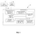
- FIG. 2is a block diagram of an electronic data flash card 10 A in accordance with an alternative embodiment of the present invention that omits the fingerprint sensor and the associated user identification process.
- the electronic data flash card 10 Aincludes a highly integrated processing unit 2 A including an input/output interface circuit 5 A and a flash memory controller 21 for integration cost reduction reasons.
- Input/output interface circuit 5 Aincludes a transceiver block, a serial interface engine block, data buffers, registers and interrupt logic.
- Input/output interface circuit 5 Ais coupled to an internal bus to allow for the various elements of input/output interface circuit 5 A to communicate with the elements of flash memory controller 21 .
- Flash memory controller 21includes a microprocessor unit, a ROM, a RAM, flash memory controller logic, error correction code logic, and general purpose input/output (GPIO) logic.
- the GPIO logicis coupled to a plurality of LEDs for status indication such as power good, read/write flash activity, etc., and other I/O devices. Flash memory controller 21 is coupled to one or more flash memory devices 3 .
- host computer 9 Aincludes a function key set 8 A, is connected to the processing unit 2 A via an interface bus or a card reader when electronic data flash card 10 A is in operation.
- Function key set 8 Ais used to selectively set electronic data flash card 10 A in one of the programming, data retrieving and data resetting modes.
- the function key set 8 Ais also operable to provide an input password to the host computer 9 A.
- the processing unit 2 Acompares the input password with the reference password stored in the flash memory device 3 , and initiates authorized operation of electronic data flash card 10 A upon verifying that the input password corresponds with the reference password.
- a host computer 9 Aincludes display unit 6 A, is connected to the processing unit 2 A when electronic data flash card 10 A is in operation via an interface bus or a card reader.
- Display unit 6 Ais used for showing the data file exchanged with the host computer 9 A, and for showing the operating status of the electronic data flash card 10 A.
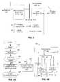
- FIG. 3shows processing unit 2 A in additional detail.
- Electronic data flash card 10 Aincludes a power regulator 22 for providing one or more power supplies to processing unit 2 A. The power supplies provide different voltages to associated units of electronic data flash card 10 A according to the power requirements. Capacitors (not shown) may be required for power stability.
- Electronic data flash card 10 Aincludes a reset circuit 23 for providing a reset signal to processing unit 2 A. Upon power up, reset circuit 23 asserts reset signal to all units. After internal voltages reach a stable level, the reset signal is then de-asserted, and resisters and capacitors (not shown) are provided for adequate reset timing adjustment.
- Electronic data flash card 10 Aalso includes a quartz crystal oscillator (not shown) to provide the fundamental frequency to a PLL within processing unit 2 A.
- input/output interface circuit 5 A, reset circuit 23 , and power regulator 22are integrated or partially integrated within processing unit 2 A.
- the high integrationsubstantially reduces the overall space needed, the complexity, and the cost of manufacturing.
- the input/output interface circuitis analog and digital mixed circuitry, which can be integrated into the MCP (Multi-Chip Package) package with the processing unit.
- the reset circuit and power regulatorare analog circuitry, which can also be integrated into the MCP (Multi-Chip Package) package with the processing unit.
- processing unit 2 Awhich includes input/output interface circuit 5 A, flash memory controller 21 , reset circuit 23 and power regulator 22 .
- a processing unit 2 , input/output interface circuit 5 , and power regulator 22 and a reset circuit 23are integrated or partially integrated using Multi-Chip Package technology or mixed signal IC technology.
- Multi Bit Cell (MBC) Flash memory deviceshave higher capacity than Single Bit Cell (SBC) flash memory devices for the same form factor.
- SBCSingle Bit Cell
- AND or Super-AND flash memoryhave been created to circumvent intellectual property issues associated with NAND flash memory.
- a large page size (2K Bytes) flash memoryhas better write performance against a small page size (512 Bytes) flash memory.
- the rapid development of flash memoryhas resulted in devices with higher capacities. To support these various flash memory types, the flash memory controller must be able to detect and access them accordingly.
- Typical flash memory devicescontains ID code which identifies the flash type, the manufacturer, and the features of the flash memory such as page size, block size organization, capacity, etc.
- the processing unit of an electronic data flash cardperforms a flash detection operation at system power up to determine whether the one or more flash memory devices of the electronic data flash card are supported by the existing flash memory controller.
- FIG. 4Aillustrates a flash detection algorithm in accordance with the present invention.
- the processing unitis reset (block 410 ).
- the ID of the flash memoryis read to identify the flash memory type (block 420 ).
- the read IDis then compared against the table of flash types that are supported by the existing flash memory controller (block 430 ). If the flash type is not supported (block 435 ), the flash memory controller will not be able to access the flash memory, and the incompatibility can be indicated by LED via an output port of the controller. If the flash type is supported, the flash memory controller will be configured to the access mode corresponding to that detected flash type (block 440 ), and then the flash memory controller begins accessing the flash memory (block 450 ).
- Electronic data flash cardsare flash memory systems using flash memories for data storage.
- electronic data flash card 10 Aincludes processing unit 2 A, flash memory 3 A, random-access memory (RAM) 24 , and read-only memory (ROM) 25 , with the boot code (BC) and operating system (OS) code residing in ROM 25 .
- processing unit 2 Afetches and executes the boot code from ROM 25 , which initializes the system components and loads the OS code from ROM 25 into RAM 24 .
- the OS codeis loaded into the RAM 24 , it takes control of the system.
- the OSincludes drivers to perform basic tasks such as controlling and allocating memory, prioritizing the processing of instructions, controlling input and output ports etc.
- the OS codealso includes the flash detection algorithm code and the flash parametric data.
- electronic data flash card 10 Aincludes a flash detection algorithm code that is separated into a static portion 26 and a dynamic portion 27 , with the static portion 26 handling contemporary flash memories, and the dynamic portion 27 taking control of the detection process after the static portion fails to identify the particular flash memory device implemented in the electronic data flash card. That is, when electronic data flash card 10 A is manufactured using an “old” type flash memory device, then the flash detection algorithm code recognizes the flash device ID during the power up process, and utilizes static portion 26 to execute read and write the “old” type flash memory device. Conversely, when a particular electronic data flash card having the novel configuration is manufactured using a “new” type flash memory device (e.g., 3 A, shown in FIG.
- a “new” type flash memory devicee.g., 3 A, shown in FIG.
- the flash detection algorithm coderecognizes the flash device ID during the power up process, and utilizes dynamic portion 27 to execute read and write operations to “new” type flash memory device 3 A.
- static portion 26 of the flash detection algorithm codeis stored in ROM 25
- dynamic portion 27 of the flash detection algorithm codeis stored in at least one flash memory device 3 A of electronic data flash card 10 A.
- the processsimply requires storing a suitable dynamic portion of the flash algorithm code in the one or more flash memory device. Because the default access and reading of the dynamic portion is already incorporated into execution of the flash detection algorithm code, the content of the dynamic portion can be altered without affecting operation of the flash detection algorithm code. Thus, overall manufacturing costs are reduced, and unnecessary development time is also eliminated.
- a method of dual-channel parallel and interleave access flashis implemented in an electronic data flash card for faster performance than is possible using conventional methods.
- a typical electronic data flash carduses a flash memory with single-channel (8-bit) data bus, as shown in FIG. 5A .
- 8-bit8-bit
- multiple-channel data busmore data bits can be read from or write to the flash memories simultaneously, thereby the access speed is enhanced.
- dual-channel (16-bit) data buscan double the access speed to the flash memory
- quad-channel (32-bit) datacan increase the access speed by 4 times, and so on.
- Electronic data flash card with dual-channel data widthcan be realized by one 16-bit wide flash memory as illustrated in FIG. 5B , by two 8-bit wide flash memories via a single control as illustrated in FIG. 5C , or by two 8-bit wide flash memories via separate controls as illustrated in FIG. 5D .
- Electronic data flash card 10 Bwhich is depicted in FIG. 5D , includes separate control and I/O connections for each flash memory device 3 B 1 and 3 B 2 , thereby enabling interleaved programming that enhances system speed and avoids peak power consumption. Flash memory devices consume higher power in the programming (writing) mode, in which data is transferred from page register into the flash cells of the memory array, than in any other operating mode (e.g., reading data from the flash cells, or writing memory to the page register from an external source).
- interleaved programming of flash memory devices 3 B 1 and 3 B 2involves “write staggering”, wherein flash memory controller 21 B enables one flash memory device (e.g., flash memory device 3 B 1 ) to program (write) data from its page register into its flash memory array while the other flash memory devices (e.g., flash memory device 3 B 2 ) are limited to non-programming operations (e.g., enabled to receive data from flash memory controller 21 B to the page register (i.e., no writing is performed in flash memory device 3 B 2 while a write operation is being performed by flash memory device 3 B 1 ).
- non-programming operationse.g., enabled to receive data from flash memory controller 21 B to the page register (i.e., no writing is performed in flash memory device 3 B 2 while a write operation is being performed by flash memory device 3 B 1 ).
- this interleave access approachallows the system to avoid peak power consumption that can be caused by writing multiple flash devices at the same time.
- FIG. 6shows an electronic data flash card (or electronic data storage medium, or integrated circuit card) 10 C according to yet another embodiment of the present invention.
- Electronic data flash card 10 Cis adapted to be accessed by a host computer 9 A via an interface bus or card reader (i.e., communication link), and includes a card body 1 C, a processing unit 2 C including a flash memory controller 21 C and an input/output interface circuit 5 C, and one or more flash memory devices 3 C in according to one or more of the embodiments described above.
- Electronic data flash card 10 Ccould be the functional subsystem for electronic data flash card 10 A (described above), and also could be a functional subsystem for other applications.
- Flash memory device 3 Cis controlled through commands generated by flash memory controller 21 C, and stores a data file in the flash memory device.
- Processing unit 2 Cis connected to flash memory device, said input/output interface circuit.
- Flash memory controller 21 C inside processing unit 2 Ccontrols flash memory device 3 C utilizing one or more of the methods described above.
- flash memory controller 21 Cexecutes a flash type algorithm that determines if flash memory device 3 C is supported by the static portion of the flash memory controller logic stored in ROM (not shown), and reads a dynamic portion of flash memory controller logic stored in flash memory device 3 C if the flash type is “new”.
- USB Bulk Only TransportBOT
- USB software communication data flowbetween a host computer and the USB interface circuit of the flash memory device (also referred to as a “USB device” below): control, interrupt, bulk, and isochronous.
- Control transferis the data flow over the control pipe from the host computer to the USB device to provide configuration and control information to a USB device.
- Interrupt transfersare small-data, non-periodic, guaranteed-latency, device-initiated communication typically used to notify the host computer of service needed by the USB device. Movement of large blocks of data across the USB interface circuit that is not time critical relies on Bulk transfers.
- Isochronous transfersare used when working with isochronous data. Isochronous transfers provide periodic, continuous communication between the host computer and the USB device. There are two data transfer protocols generally supported by USB interface circuits: Control/Bulk/Interrupt (CBI) protocol and Bulk-Only Transfer (BOT) protocol.
- CBIControl/Bulk/Interrupt
- BOTBulk-Only Transfer
- the mass storage class CBI transport specificationis approved for use with full-speed floppy disk drives, but is not used in high-speed capable devices, or in devices other than floppy disk drives (according to USB specifications).
- a USB flash devicetransfers high-speed data between computers using only the Bulk-Only Transfer (BOT) protocol.
- BOTis a more efficient and faster transfer protocol than CBI protocol because BOT transport of command, data, status rely on Bulk endpoints in addition to default Control endpoints.
- processing unit 2 Cis selectively operable in a programming mode, where processing unit 2 C causes input/output interface circuit 5 C to receive the data file from host computer 9 A, and to store the data file in flash memory device 3 C through write commands issued from host computer 9 A to flash memory controller 21 C, a data retrieving mode, where processing unit 2 C receives the data in flash memory device 3 C through read command issued from host computer 9 A to flash memory controller 21 C and to access the data file stored in flash memory device 3 C, and activates input/output interface circuit 5 C to transmit the data file to host computer 9 A, and a data resetting mode where the data file is erased from flash memory device 3 C.
- inventions of the intelligent processing unit 2 C in accordance with the present inventioninclude:
- a system and methodfor controlling flash memory in an electronic data flash card.
- the system and methodprovide a flash memory controller including a processor for receiving at least one request from a host system, and an index, which comprises look-up tables (LUTs) and a physical usage table (PUT).
- the indextranslates logical block addresses (LBAs) provided by the host system to physical block addresses (PBAs) in the flash memory.
- LBAslogical block addresses
- PBAsphysical block addresses
- the indexalso contains information regarding the flash memory configuration.
- the processorselectively utilizes the index to determine the sectors of the flash memory that are available for programming, reprogramming, or reading.
- the flash memory controllerfurther comprises a recycling first-in-first-out (FIFO) that recycles blocks of obsolete sectors so that they are available for reprogramming.
- FIFOrecycling first-in-first-out
- the recycling operationinvolves copy and erase operations, and is performed in the background and thus hidden from the host system. Accordingly, the management of the flash memory and related intelligence resides in the flash memory controller instead of in the host system. As a result, the host system interacts with the flash memory controller without the host system having information regarding the physical configuration of the flash memory. Consequently, speeds at which data is written to and read from the flash memory is significantly increased while the flash memory remains compatible with the USB standard and ASIC architecture.
- BlockA basic memory erase unit. Each block contains numerous sectors, e.g., 16, 32, 64, etc. If any sector encounters write error, the whole block is declared a bad block and all valid sectors within the block are relocated to another block.
- SectorA sub-unit of a block. Each sector typically has two fields—a data field and a spare field.
- Obsolete sectorA sector that is programmed with data but the data has been subsequently updated. When the data is updated, the obsolete data remains in the obsolete sector and the updated data is written to new sectors, which become valid sectors.
- Non-valid blocksBlocks that contain obsolete sectors.
- Valid sectorA sector that has been programmed with data and the data is current, i.e., not obsolete.
- Flash memorycan be block erased only a limited number of times. For example, one million is a typical maximum number of erases for NAND flash memory.
- Spare blocksReserved space in flash memory. Spare blocks enable flash memory systems to prepare for bad blocks.
- ClusterMultiple data sectors used as file access pointers by an operating system to improve memory performance. In small mass-storage memory operation, a cluster normally is a combination of two data sectors, which is a minimum file size unit.
- FATFile allocation table having file address-linked pointers.
- a clusteris the unit for a FAT.
- FAT16means that a cluster address can be 16 bits.
- Directory and subdirectoryFile pointers as defined by an operating system.
- Master boot record (MBR)A fixed location to store a root directory pointer and associated boot file if bootable. This fixed location can be the last sector of the first block, or the last sector of the second block if first block is bad.
- PacketA variable length format for a USB basic transaction unit.
- a normal transaction in the USB specificationtypically consists of three packets—a token packet, a data packet, and a handshake packet.
- a token packethas IN, OUT, and SETUP formats.
- a data packet sizecan be varying in size, e.g., 64 bytes in USB revision 1.1, and 512 bytes in USB revision 2.0.
- a handshake packethas ACK or NAK formats to inform host of the completion of a transaction.
- FrameA bulk transaction that is used that has a high priority for occupying a frame if USB traffic is low. A bulk transaction can also wait for a later frame if USB traffic is high.
- EndpointThree endpoints include control, bulk-in, and bulk-out. The control endpoint is dedicated to system initial enumeration.
- the bulk-in endpointis dedicated to host system read data pipe.
- the bulk-out endpointis dedicated to a host system write data pipe.
- Command block wrapperCBW: A packet contains a command block and associated information, such as Data Transfer Length (512 bytes for example from byte 8 - 11 ). A CBW always starts at the packet boundary, and ends as short packet with exactly 31 bytes transferred. All CBW transfers shall be ordered with LSB (byte 0 ) first.
- Command Status Wrapper (CSW)A CSW starts at packet boundary.
- Reduced block command (RBC) SCSI protocola 10 byte command descriptor.
- FIG. 7is a block diagram showing a electronic data flash card (memory system) 100 including a flash memory controller 110 and a flash memory device 112 in accordance with the present invention.
- the host system 52provides resources to process write and read transactions, and erase operations via the flash memory controller 110 .
- the flash memory controller 110is coupled to a host system 52 via a host system interface 116 .
- the host system 52can be a personal computer or other type of computer system.
- the operating system of the host system 52can be Windows or MacOS but is not limited to these operating systems.
- the flash memory system 100complies with the USB mass-storage class standard and the host system interface 116 is a USB connection.
- the USB specificationcan be revision 1.1 or 2.0 and above.
- the flash memory controller 110 and the flash memory 112can be either bus-powered or self-powered, and can be used as a mass storage device.
- the advantage of being used as a mass storage deviceis that it is a low-power device, it is easy to carry, and it has storage capacity larger than a traditional floppy disk.
- the flash memory controller 110includes a device transceiver 120 , which converts analog signals to digital streams and provides a phase lock loop (PLL) circuit for generating precision clocks for internal data latching.
- PLLphase lock loop
- the flash memory controller 110also includes a serial interface engine (SIE) 122 , which provides serial and parallel data conversion, packet decoding/generation, cyclic redundancy code (CRC) generation/checking, non-return-to-zero (NRZI) encoding/decoding, and bit stuffing according to the USB standard.
- SIEserial interface engine
- Endpoints 124 and 125receive information from the host system 52 regarding class type (e.g., mass-storage class), flash memory configuration information, and default control information.
- An Endpoint 126receives information from the host system 52 regarding read transactions, and an endpoint 128 receives information from the host system 52 regarding write transactions.
- a bulk-only transport (BOT) unit 130receives command block wrappers (CBW) and includes a data transfer length register 132 and a logical block address (LBA) register 134 .
- CBWcommand block wrappers
- LBAlogical block address
- the allocation of PBAs to LBAsis performed entirely by flash memory controller 110 , thus allowing host system 52 to interact with flash memory device 110 (i.e., perform read, write and erase operations) without host system 52 having information regarding the actual physical location (configuration) of the data stored in flash memory device 112 . That is, flash memory controller 110 utilizes arbitration logic and data that is entirely stored in electronic data flash card 100 (i.e., not received from host system 52 ) to identify bad blocks of memory cells in flash memory device 112 , to assign LBAs to the PBAs associated with good blocks of memory cells, to recycle non-valid blocks, and to perform wear leveling. Because each of these operations is performed independent of host system 52 , the operation of host system 52 is enhanced.
- a sector FIFO 140provides a caching feature when the host system 52 attempts to write data to the flash memory 112 .
- a FIFO-not-empty interrupt signal 142triggers an interrupt routine at an interrupt handler 148 of a processor 150 .
- the interrupt routineresponds to the host system 52 confirming that data was written to the flash memory 112 .
- the processor 150executes a write transaction.
- a write look-up table (LUT) 170 , a read LUT 172 , and a physical usage table (PUT) 180provide an index showing the configuration of the flash memory 112 .
- the data stored in write and read LUTs 170 and 172 and PUT 180is controlled by the arbitration logic (discussed above) utilized by flash memory controller 110 .
- the write and read LUTs 170 and 172facilitate write and read transactions, respectively, between the host system 52 and the flash memory 112 .
- the write and read LUTs 170 and 172translate logical block addresses (LBAs) provided by the host system 52 to physical block addresses (PBAs) of the flash memory 112 .
- the PUT 180performs physical sector mapping and provides a bitmap indicating programmed sectors, i.e., sectors to which data has already been written.
- a flash interface controller 186interfaces with the flash memory 112 to carry out commands from the processor 150 .
- the flash interface controller 186receives PBAs from the write and read LUTs 170 and 172 to service write and read requests.
- a recycling FIFO 190recycles blocks having obsolete sectors so that they can be reprogrammed, i.e., written to with new data.
- the recycling operationsare executed immediately after and independently from write transactions so as to not interfere with the servicing of write transactions by the flash memory controller 110 .
- the write and read LUTs 170 and 172 , the PUT 180 , and the recycling FIFO 190are implemented with volatile random access memory (RAM), such as synchronous RAM (SRAM).
- RAMvolatile random access memory
- SRAMsynchronous RAM
- the flash memory 112can be implemented using one or more devices, each having one or more flash arrays.
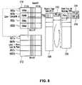
- FIG. 8is a block diagram showing in more detail the write LUT 170 , the read LUT 172 , the PUT 180 , and the recycling FIFO 190 of FIG. 7 in accordance with the present invention.
- the write LUT 170provides an index for the flash memory during write transactions and translates LBAs provided by the host system to PBAs of the flash memory.
- the write LUT 170contains LBAs 302 a , 302 b , 302 c , and 302 d . For ease of illustration, only four LBAs per LUT are shown.
- Each of the LBAs 302 a - dincludes optional block-offset bits (bit 5 to bit 0 ). The block-offset bits correspond to particular sectors in a block.
- Each LBA 302 a - dis associated with a PBA 304 a - d . Accordingly, each LBAa-d points to an associated PBAa-d, respectively.
- a PBAis 32-bits long.
- a sector field 306contains a string of bits indicating programmed sectors within a block.
- the write LUT 170records only the starting LBA for a particular write transaction. For example, if a particular write transaction requires two or more consecutive blocks, the write LUT 170 records the starting LBA.
- the read LUT 172provides an index for the flash memory during read transactions and translates LBAs provided by the host system to PBAs of the flash memory.
- the read LUT 172contains LBAs 302 ′ a , 302 ′ b , 302 ′ c , and 302 ′ d .
- the read LUT 172has the same fields as the write LUT 170 .
- the read LUT 172is updated to reflect the changes to the write LUT 170 such that the write and read LUTs 170 and 172 become identical. Once the read LUT is updated, it can be used as an index for read transactions.
- the PUT 180performs physical sector mapping and provides a bitmap indicating programmed sectors, i.e., sectors to which data has already been written. Whenever a write transaction occurs, the PUT 180 records the usage information indicating the programmed sectors. This facilitates write transactions in that the processor of the flash memory controller can determine from the PUT 180 which sectors are available for programming or reprogramming.
- the recycling FIFO 190recycles non-valid blocks and the recycling process occurs after each successful write transaction. Whenever a block having an obsolete sector is encountered, information regarding that block's physical address is placed in the recycling FIFO 190 indicating it's a non-valid block. After finishing the valid sector copy-relocate operations, recycling FIFO 190 provides address information for performing non-valid block erase operations.
- the recycling FIFO 190uses a write pointer 192 as updating FIFO address pointer for non-valid blocks and read pointers 194 and 196 as two read address reference pointers. Read pointer 2 196 is used for background recycling reading reference and read pointer 1 194 is a reference for valid block if the erase-recycling is successful.
- Read pointer 1 194should never exceed read pointer 2 196 . Both read pointers 194 and 196 should not overtake write pointer 192 .
- the copy-relocate (for remaining valid sectors within non-valid blocks) and erase-recycling operationsare performed in the background, i.e., independently from write transactions so as to not interfere with the write transactions.
- FIG. 9is a block diagram showing in more detail the flash memory 112 of FIG. 7 in accordance with the present invention.
- the flash memory 112has a data structure that comprises a data field 402 and a spare field 404 for each PBA.
- Each fieldholds a certain number of bytes and the specific number will depend on the application. For example, a data field may have 512 bytes, 2,112, or more bytes, and the spare field can have 16, 64, or more bytes.
- the data field 402stores raw data and the spare field 404 stores information related to memory management.
- the spare field 404includes a bad block indicator field 406 , an error correction code (ECC) field 408 , an erase count field 410 , and an LBA field 412 . Because the LUT and PUT tables 170 , 172 , and 180 are stored volatile memory and thus do not preserve the valid sector information, the LBA field 412 is used to reconstruct the write and read LUTs 170 , 172 and the PUT 180 during system initialization and power failure.
- ECCerror correction code
- the bad block indicator field 406indicates bad blocks.
- a bad blockoccurs when an attempt to write to a particular sector or to erase a particular block fails.
- a special bad block indicator field 414is located at the last block, a location, which is easier for the firmware to read, especially where there is one bit per sector.
- four copies of bad block indicatorsare saved in the last block of the flash memory. Of course fewer or more copies can be utilized.
- the need for flags in the flash memoryis eliminated by the present invention.
- the only flag usedis the valid sector flag used in the LUTs to assist in firmware decision making. This minimizes the complexity with regard to write and read transactions.
- FIG. 10is a high-level flow chart showing a method for managing flash memory in accordance with the present invention.
- a host systemreceives utilizing a processor within a memory controller, in a step 502 .
- the requestcan be a write or read request.
- the sectors of the flash memory that are available for programming, reprogramming, or readingare determined utilizing the processor and an index within the memory controller, in a step 504 .
- the host systeminteracts with the flash memory controller without the host system having information regarding the configuration of the flash memory.
- the flash memory controllerreceives a request from the host system in compliance with the USB mass-storage class.
- the flash memory controllerreceives a request from the host system in compliance with the USB mass-storage class.
- FIG. 11is a flow chart showing a method for transmitting USB mass-storage class service requests in accordance with the present invention.
- the memory controllerreceives a request from the host system, in a step 602 .
- This stepcan be referred to as a command transport step 602 .
- the requestcan be a write or read request. If the request is a write request, a write transaction is performed, in a step 604 . This step can be referred to as a data-out step 604 . If the request is a read request, a read transaction is performed, in a step 606 . This step can be referred to as a data-in step 606 .
- an acknowledge packetis sent to the host system by the memory controller to confirm completion of the transaction, in a step 608 . This step can be referred to as a status transport step 608 .
- the command transport step 602 and the data-out step 604are generally referred to as bulk-out transport steps since data packets are sent out from the host system.
- the data-in step 606 and the status transport step 608are generally referred to as bulk-in transport steps since data packets are sent into the host system.
- FIGS. 12A-Care block diagrams showing a command block wrapper (CBW) 702 , a reduced block command read format (RBC) 704 , and a command status wrapper (CSW) 706 in accordance with the present invention.
- the USB standardinvolves three packets per request, which include the CBW 702 , the RBC 704 , and the CSW 706 .
- the CBW 702 , the RBC 704 , and the CSW 706 packetsare also generally referred to as token, data, and acknowledge handshake packets, respectively, and are utilized in the command transport, data-in/out, and status transport steps 602 - 608 of FIG. 11 , respectively.
- the CBW 702contains information regarding what data from the host system is to follow.
- the CBW 702is 31 bytes long and includes command decoding and direction, and a unique LBA.
- the LBA in the CBW 702can include information regarding the file allocation table (FAT) and directory pointers.
- the CBW 702also contains the read/write direction in byte 15 as part of the RBC command.
- the RBC 704contains information such as data to be written to the flash memory.
- the RBC 704is a SCSI RBC.
- the length of the datacan vary and is defined by different USB standard versions, e.g., 64 bytes in USB 1.1, 512 bytes in USB 2.0.
- the CSW 706contains information regarding acknowledge procedures and information for terminating a transaction.
- Byte 12is a status byte.
- FIG. 13is a flow chart showing a method for reading, writing, and erasing in accordance with the present invention.
- a requestis received from the host system, in a step 802 .
- the requestincludes the CBW 702 , the RBC 704 , and the CSW 706 .
- the type of command, whether a write or read requestis determined, in a step 804 .
- registers for the CBW and CSWare initialized, in a step 806 .
- the sector data FIFO in the flash memory controlleris filled, and when 512 bytes of data are ready, a write pointer for the sector data FIFO is incremented and an interrupt is sent to the processor in the flash memory controller, in a step 810 .
- the write transactionis executed, in a step 812 .
- an acknowledge packetis sent to the host system confirming that the write transaction was successfully completed, in a step 814 .
- the firmware of the flash memory controllerchecks the recycling FIFO status, in a step 820 . If the recycling FIFO is not empty, the recycling FIFO recycles obsolete sectors, in a step 822 .
- the LBA in the CBWis compared with all existing entries of the sector FIFO, in a step 828 . If there is a match, the requested data is returned to the host system, in a step 830 . Next, an acknowledge packet is sent to the host system confirming that the read transaction was successfully completed, in a step 832 . If there is no match, the requested data is read from the flash memory, in a step 834 . Finally, a status/acknowledge packet is sent to the host system confirming that the read transaction was successfully completed, in a step 836 .
- FIG. 14is a high-level flow chart showing a method including a first phase of a write transaction, a second phase of the write transaction, a read transaction, and a recycling operation in accordance with the present invention.
- a CBWis received, in a step 902 .
- it is determined whether the request is a write requestin a step 904 .
- the sector FIFOis checked, in a step 906 . If the sector FIFO is not empty, the write transaction is then initiated.
- the write transactionhas two phases.
- datais written to a particular number of sectors and an acknowledge packet is then sent to the processor of the flash memory controller and to the host system indicating that the write transaction has been completed, in a step 910 .
- the second phase of the write transactionis initiated. Accordingly, valid sectors are copied from a non-valid block to a new address in another block, in a step 920 .
- the copy step 920is accomplished in the background to maintain data coherency.
- the requested datais fetched from the flash memory using the PBA in the read LUT, in a step 930 .
- the second phaseis executed, in the step 920 .
- Obsolete sectorsare recycled by the recycling FIFO, in a step 940 , when there are no requests being serviced.
- the firmware of the flash memory controllercan return to servicing other requests from the host system.
- FIGS. 15A-Dare block diagrams illustrating exemplary results from first and second phases of a write transaction in accordance with the present invention. To further clarify the above-described features of the present invention, the following example is provided.
- FIGS. 15A-Dshow four write transactions including varying-length data strings.
- FIG. 15Dshows a write transaction where data is updated. For ease of illustration, only four sectors per block are shown.
- Two blocks (PBA 0 and PBA 1 ) of the flash memory 112have four sectors each.
- the write LUT 170writes to six physical sectors of the flash memory 112 , beginning the first physical block (PBA 0 ).
- PBA 0the first physical block
- the flash memory 112is initially empty.
- the labels A 0 -A 5represent data written during the first write transaction.
- Bits in the PUT 180 corresponding to the sectors of the flash memory 112show a 1 to indicate that those sectors have been programmed, i.e., occupied.
- the firmware of the flash memory controllerutilizes the PUT 180 to determine the available sectors. Accordingly, those sectors have data that cannot be reprogrammed until first erased but those sectors can be later read.
- the write LUT 170 having written to the sectorsindicates the valid sectors with 1s.
- the read LUT 172 informationis copied from the write LUT 170 information to reflect the most recent changes. However, the read LUT 172 is copied from the previous version of the write LUT 170 and is ultimately synchronous with the write LUT 170 once the write phases are completed. Accordingly, until the read LUT 172 is updated, it will show the pre-update information of the write LUT 170 with 0s shown to indicate empty sectors.
- the write LUT 170has written new data B in the next available sector in PBA 1 . This is the second write transaction.
- the write LUT 170 , the PUT 180 , and flash memory blockreflect this update.
- the read LUT 172has been updated with the prior change but has not yet been updated to reflect the current change.
- the write LUT 170has written new data C 0 and C 1 to the next available sectors. This is the third write transaction. Note that the data C 0 and C 1 cross the block boundary as does the data A 0 -A 5 . Again, the write LUT 170 , the PUT 180 , and flash memory blocks reflect this update. The read LUT 172 has been updated with the prior change but has not yet been updated to reflect the current change.
- the write LUT 170has written data to update existing data A 0 -A 4 with updated data a 0 -a 4 .
- the write LUT 170 , the PUT 180 , and the flash memory blocksreflect this update, and the read LUT 172 has been updated with the prior change but has not yet been updated to reflect the current change.
- the blocks PBA 0 and PBA 1have become non-valid because the data in some of their sectors became obsolete. Accordingly, those blocks can then be recycled by the recycling FIFO 190 .
- the recycling FIFO 190has changed corresponding bits to 0 to indicate this.
- the write pointer 192 of the recycling FIFO 190is incremented to point to the next available position to store the nextnon-valid block address.
- the data A 5 , B, and C 0are copied to new blocks, which are blocks PBA 3 - 4 to maintain consistency in the write LUT 170 .
- the write LUT 170 , the PUT 180 , and the flash memory blocksreflect this update.
- the read LUT 172will then be updated to reflect the current change. Also both phases of the write transaction are complete, the write and read LUTs 170 and 172 will be identical.
- FIG. 16is a flow chart showing a method for implementing the first phase of the write transaction of PBA and sector count updating procedure of FIG. 14 in accordance with the present invention, which basically does index mapping between LBAx and PBAx so that both read and write addresses are kept in tracking.
- Table 1(below) is a simplified example of one entry of LUTs and FIFO with assumed 8 sectors per block in flash memory. An entry of 1 means sector data is valid, and 0 means sector is available for use. Please note that LUTs (mapping table) are pointed by LBAx, but FIFO is pointed by Wr_ptr and Rd_ptrs.
- an LBA and sector count (SC) from host systemis evaluated, in a step 1102 .
- LBA block offset bitsare encoded into a sector count, in a step 1104 .
- the LBApoints to a PBA in the flash memory. For example, if LBA is 0010,0101 and sector number is 16, then 0010 will be the initial LBAx block address for both LUT entry pointers. If the sector field of the PUT is 0, i.e., the sector is available, then the sector count register is equal to the CBW sector count and the PBA field of the write LUT will be loaded, in a step 1106 .
- the sector field of the write LUTis 1, this means the flash sector is used by previous programming, and the write pointer is positioned to the block to be erased, in a step 1108 .
- the entry of recycling FIFO pointed to by write_pointerwill be filled by current PBAx, in a step 1110 .
- the block pointed to by the write pointerwill be erased.
- the sector field in the PUTis set to 1, in a step 1112 , where the PBA indicates that the sector is being used.
- the sector numberin incremented, in a step 1114 .
- the sector numberis compared against the block boundary, in a step 1116 . If the sector number is aligned with the block boundary, the write pointer is incremented, in a step 1118 .
- the LBA in the write LUTis incremented, in a step 1120 , when flash block boundary is reached.
- the write LUTis updated with the correct sector number position, in a step 1122 . If the sector number is not aligned with the block boundary, steps 1118 and 1120 are bypassed and the write LUT is updated with the correct sector number position, in a step 1122 .
- the sector field of write LUTis 0, which means that the flash sector is not used by previous programming, i.e., the write transaction is not finished.
- the sector countis then compared to the sector count in the CBW, in a step 1124 . If they are the same, PBAx field of LUT pointed by LBAx will be updated in a step 1126 , then proceed to step 1128 . If the sector count register is not equal to the CBW sector count in step 1124 , the sector field will be set to 1 in both index look up tables and data will be written into the flash memory. Next, the sector number is incremented, in a step 1128 . After successful write into flash memory, sector count from CBW is decremented, in a step 1130 .
- the sector countis checked, in a step 1132 . If the sector count is equal to 0, the first phase of the write transaction terminates. If the sector count is not equal to 0, that means the host system did not send the correct amount of data. Accordingly, the sector FIFO is checked to determine whether there is any more available data, in a step 1134 . If not, a time-out sequence is executed, in a step 1136 , to flag an abnormal flow termination, and the sector FIFO is continually checked until sufficient data is available. If there is more available data in the sector FIFO, the sector number is compared against the block boundary, as in the step 1116 .
- FIG. 17is a flow chart showing a method for implementing the second phase of the write transaction of FIG. 14 in accordance with the present invention.
- the pointer values of the write and read pointersare compared, in a step 1202 .
- the sector field from the recycling FIFO entry pointed to by the read pointerindicates that a valid sector needs to be copied to a new PBA in order to achieve consistency in the write LUT.
- the read LUTis updated to be identical to the write LUT, in a step 1204 .
- the sector number pointed to by the read pointeris checked, in a step 1206 . If the sector number is equal to 1, the data in that sector is copied to a new block, in a step 1208 .
- the sector number in the PUTis set to 1, in a step 1210 .
- the write LUT sector fieldis updated, in a step 1212 .
- the read LUT sector fieldis updated, in a step 1214 .
- the sector numberis incremented, in a step 1216 . Referring back to the step 1206 , if the sector number is not equal to 1, the sector number is incremented, as in the step 1216 .
- the sector copying processwill be completed as long as the sector number reaches the block boundary.
- the sector numberis compared against the block boundary, in a step 1218 . If the sector number is aligned with the block boundary, the read pointer is incremented, in a step 1220 . Next, the read pointer is compared with the write pointer, as in the step 1202 . If in the step 1218 , the sector number is not aligned with the block boundary, the sector number pointed to by the read pointer is checked, as in the step 1206 .
- FIG. 18is a flow chart showing a method for implementing the read transaction of FIG. 14 in accordance with the present invention.
- a CBWis received and recognized as read request, and an LBA and sector count is loaded from the CBW, in a step 1302 .
- the LBA of the write LUTis translated into a corresponding PBA and sector number, in a step 1304 .
- the sector field bitis checked, in a step 1306 . If the sector field bit is equal to 1, the data is read, the sector count is decremented, and the sector number is incremented in preparation for the next read transaction, in a step 1308 .
- the sector field bitis not equal to 1, i.e., equal to 0, the LBA of the read LUT is translated into a corresponding PBA, in a step 1309 . Then the data is read, the sector count is decremented, and the sector number is incremented, as in the step 1308 .
- an error correction code (ECC) calculationis performed, in a step 1310 .
- ECCerror correction code
- the ECC resultis compared with a value read from the flash spare field, in a step 1312 . If the values are identical, the sector count is checked, in a step 1314 . If the values are not identical, an ECC correction is performed, in a step 1316 , and then the sector count is checked, as in the step 1314 . If the sector count has reached 0, i.e., equals 0, the read process terminates. If the sector count has not reached 0, the block boundary will also be checked, in a step 1317 . If the sector number is not aligned with the block boundary, the read LUT is updated with the correct sector number position, in a step 1318 . If the sector number is aligned with the block boundary, the LBA in the read LUT is incremented, in a step 1320 , and then the read LUT is updated with the correct sector number position, as in the step 1318 .
- a read transactionis executed immediate after a first phase of a write transaction.
- the read transactionhas a higher priority than the second phase of a previous write transaction. This ensures optimal responses by the flash memory system.
- a read transactionis significantly faster than a write transaction and read transactions do not result in bad block situations, which only occur during write transactions and erase operations.
- a read transactiondiffers from a disk cache function whenever the contents in the sector FIFO are available. This can happen when the LBA in the read LUT matches the previous LBA in the write LUT.
- the disk cache conceptis borrowed from magnetic hard disk concepts and applied to small-capacity flash storage. This feature is typically disabled to save cache cost.
- FIG. 19is a flow chart showing a method for implementing the recycling operation of FIG. 14 in accordance with the present invention.
- the recycling FIFOis checked, in a step 1402 . If the recycling FIFO is empty, the recycling operation terminates. If the recycling FIFO is not empty, the read pointer 2 is checked, in a step 1404 , background erasing operation happens in this case, once erasing is successful, read pointer 1 is incremented for another valid block reprogramming address checking operation. The two read pointers should not overtake the write pointer. However, the write pointer may loop back to its original starting position if both read pointers are executed. If the read pointer 2 is positioned over the write pointer, the recycling operation terminates.
- the read pointer 2is not positioned over the write pointer, the corresponding bit in the PUT is cleared, i.e., 0, in a step 1406 , to indicate that the physical block is now available for reprogramming.
- the read pointer 2is positioned to point to the block to be erased, in a step 1408 .
- the read pointer 2is incremented after successful erasing, in a step 1410 , for the next write address checking operation.
- Pointer comparison for the recycling FIFOcan be achieved by adding one more bit to the index of both the write and read pointers. For example, if the recycling FIFO contains eight PBA entries, four bits instead of three bits will be used for the pointers. The write pointer will start from 0 and increment to 7 and then cycle back to 0. The write pointer value should always be at least equal to or greater than the read pointers. When they are equal, it means that the recycling FIFO is empty. The depth, i.e., the number of entries, of the recycling FIFO affects the tradeoff between line-copy speed and the erase speed. Too few entries makes the recycling FIFO less optimal.
- the flash memory controller of the present inventioncan perform multiple-block data access.
- the conventional flash memory devicehas a 512-byte page register built-in.
- the data write to the flash memory devicehas to write to the page register first and then to a flash memory cell.
- the conventional flash memory controllercontrols the flash memory access cycles.
- the conventional flash memory controllertransfers one single block (512 bytes) of data to the page register of the flash memory device at a time. No other access to the flash memory is allowed once the 512 bytes page register is filled. Consequently, the conventional flash memory controller, which uses the single-block data access methodology, limits the performance of flash memory devices.
- the flash memory controllerutilizes a 2K or larger size page register.
- the flash memory controller of the present inventionfunctions as a multiple-block access controller by sending multiple blocks of data simultaneously to a flash memory to fill up the page register. This significantly improves the performance of the data transfer. Compared to the conventional single-block data-transfer controller, which transfers a single block at a time, the data transfer performance using the flash memory controller of the present invention is significantly improved.
- the flash memory controller of the present inventioncan also provide dual channel processing to improve performance of the flash memory system. Dual channeling provides a second channel, or “freeway,” for executing transactions between the flash memory controller and the flash memory device.
- a conventional flash memory controlleruses a single memory bus such that one or more flash memory devices attached to it. However, the conventional architecture limits the performance of the conventional flash memory controller.
- each set of memory busesis coupled to separate flash memory devices.
- the memory controllercan access flash memory devices together or separately.
- transactionscan be executed twice as fast utilizing dual channel processing.
- each memory buscan also be further expanded to multiple sets of memory buses.
- the flash memory controller of the present inventioncan also interleave operations.
- a conventional flash memory controlleruses a single set of memory buses such that one or more flash memory devices are attached to it.
- the conventional flash memory controllercan only access the flash memory devices one at a time. Accordingly, the conventional architecture limits the performance of the conventional flash memory controller.
- At least one or two extra sets of memory control signalsare utilized.
- a shared memory bus having at least two banks of flash memory devicesare attached to the shared memory bus.
- the flash memory controller of the present inventioncan access one bank of flash memory devices while the other bank is busy reading or writing. Accordingly, the flash memory controller of the present invention fully utilizes the shared memory bus and thus significantly increase the performance. Furthermore, the number of pins of the flash memory controller are reduced by sharing memory I/O and control signals. This minimizes the cost to make flash memory devices.
- one in the artcan integrate functions of multiple block access, multiple bank interleaving, and multiple channel operations together in a memory access cycle of a single chip to achieve maximum performance.
- the flash memory controllercan be applied to USB as well as PCI-Express plug and receptacle systems. Also, the flash memory controller can be applied to other embodiments involving SD, MMC, MS, CF, IDE, and SATA plug and receptacle systems.
- the present inventionprovides numerous benefits. For example, it shifts the management of the flash memory and related intelligence from the host system to the flash memory controller so that the host system interacts with the flash memory controller without the host system having information regarding the configuration of the flash memory.
- the flash memory controllerprovides LBA-to-PBA translation, obsolete sector recycling, and wear leveling. Furthermore, the recycling operations are performed in the background. Furthermore, flash specific packet definitions and flags in the flash memory are eliminated.
- the flash memory controllerprovides multiple-block data access, dual channel processing, and multiple bank interleaving. Consequently, speeds at which data is written to and read from the flash memory is significantly increased while the flash memory remains compatible with the USB standard and ASIC architecture.
- a system and method in accordance with the present invention for controlling flash memorycomprise a processor for receiving at least one request from a host system, and an index, which comprises look-up tables (LUTs) and a physical usage table (PUT).
- the indextranslates logical block addresses (LBAs) provided by the host system to physical block addresses (PBAs) in the flash memory.
- LBAslogical block addresses
- PBAsphysical block addresses
- the indexalso contains intelligence regarding the flash memory configuration.
- the processorcan utilize the index to determine the sectors of the flash memory that are available for programming, reprogramming, or reading.
- the flash memory controllerfurther comprises a recycling first-in-first-out (FIFO) that recycles blocks having obsolete sectors so that they are available for reprogramming.
- FIFOrecycling first-in-first-out
- the recycling operationinvolves copy and erase operations, and is performed in the background and thus hidden from the host system. Accordingly, the management of the flash memory and related intelligence resides in the flash memory controller instead of in the host system. As a result, the host system interacts with the flash memory controller without the host system having information regarding the configuration of the flash memory. Consequently, speeds at which data is written to and read from the flash memory is significantly increased while the flash memory remains compatible with the USB standard and ASIC architecture.
Landscapes
- Engineering & Computer Science (AREA)
- Theoretical Computer Science (AREA)
- Physics & Mathematics (AREA)
- General Physics & Mathematics (AREA)
- Computer Security & Cryptography (AREA)
- Computer Hardware Design (AREA)
- General Engineering & Computer Science (AREA)
- Software Systems (AREA)
- Human Computer Interaction (AREA)
- Microelectronics & Electronic Packaging (AREA)
- Multimedia (AREA)
- Storage Device Security (AREA)
- Techniques For Improving Reliability Of Storages (AREA)
- Read Only Memory (AREA)
Abstract
Description
- (1) providing high integration, which substantially reduces the overall space needed and reduces the complexity and the cost of manufacturing.
- (2) utilizing an intelligent algorithm to detect and access the different flash types, which broadens the sourcing and the supply of flash memory;
- (3) by storing the portion of software program along with data in flash memory which results in the cost of the controller being reduced; and
- (4) utilizing more advanced flash control logic which is implemented to raise the throughput for the flash memory access.
| TABLE 1 | ||
| PBA w/o sector offset | ||
| 0 | |||||||||
| 1 | 0 | 0 | 1 | 1 | 0 | 0 | 0 | |
Claims (10)
Priority Applications (56)
| Application Number | Priority Date | Filing Date | Title |
|---|---|---|---|
| US11/466,759US7702831B2 (en) | 2000-01-06 | 2006-08-23 | Flash memory controller for electronic data flash card |
| US11/625,309US7483329B2 (en) | 2000-01-06 | 2007-01-20 | Flash card and controller with integrated voltage converter for attachment to a bus that can operate at either of two power-supply voltages |
| US11/625,310US20070168614A1 (en) | 2000-01-06 | 2007-01-20 | Secure-Digital (SD) Flash Card with Auto-Adaptive Protocol and Capacity |
| US11/626,347US7702984B1 (en) | 2000-01-06 | 2007-01-23 | High volume testing for USB electronic data flash cards |
| US11/657,243US7962836B1 (en) | 2000-01-06 | 2007-01-24 | Electronic data flash card with bose, ray-chaudhuri, hocquenghem (BCH) error detection/correction |
| US11/668,316US7861312B2 (en) | 2000-01-06 | 2007-01-29 | MP3 player with digital rights management |
| US11/674,645US7620769B2 (en) | 2000-01-06 | 2007-02-13 | Recycling partially-stale flash blocks using a sliding window for multi-level-cell (MLC) flash memory |
| US11/677,658US20070156587A1 (en) | 2000-01-06 | 2007-02-22 | Content Protection Using Encryption Key Embedded with Content File |
| US11/679,716US20070233955A1 (en) | 2000-01-06 | 2007-02-27 | Mixed-Mode ROM/RAM Booting Using an Integrated Flash Controller with NAND-Flash, RAM, and SD Interfaces |
| US11/682,261US7420803B2 (en) | 2000-01-06 | 2007-03-05 | Universal serial bus flash drive with deploying and retracting functionalities |
| US11/737,336US7333364B2 (en) | 2000-01-06 | 2007-04-19 | Cell-downgrading and reference-voltage adjustment for a multi-bit-cell flash memory |
| US11/773,830US7872871B2 (en) | 2000-01-06 | 2007-07-05 | Molding methods to manufacture single-chip chip-on-board USB device |
| CNB200710137211XACN100487678C (en) | 2006-08-23 | 2007-07-11 | Electronic data flash memory card with flash memory controller |
| US11/831,888US7830666B2 (en) | 2000-01-06 | 2007-07-31 | Manufacturing process for single-chip MMC/SD flash memory device with molded asymmetric circuit board |
| US11/851,336US20080041966A1 (en) | 2000-01-06 | 2007-09-06 | Mid-Seam Package Methods of Manufacture for Memory Cards Using Ultraviolet Cure Adhesive and Ultra-Sonic Press |
| TW96135503ATW200915080A (en) | 2006-08-23 | 2007-09-21 | Flash memory controller for electronic data flash card |
| US11/864,671US20080071973A1 (en) | 2000-01-06 | 2007-09-28 | Electronic data flash card with various flash memory cells |
| US11/866,927US8043099B1 (en) | 2004-02-12 | 2007-10-03 | Extended USB plug, USB PCBA, and USB flash drive with dual-personality |
| US11/867,610US20080147964A1 (en) | 2004-02-26 | 2007-10-04 | Using various flash memory cells to build usb data flash cards with multiple partitions and autorun function |
| US11/871,117US7788553B2 (en) | 2000-01-06 | 2007-10-11 | Mass production testing of USB flash cards with various flash memory cells |
| US11/871,011US7934074B2 (en) | 1999-08-04 | 2007-10-11 | Flash module with plane-interleaved sequential writes to restricted-write flash chips |
| US11/871,627US7966462B2 (en) | 1999-08-04 | 2007-10-12 | Multi-channel flash module with plane-interleaved sequential ECC writes and background recycling to restricted-write flash chips |
| US11/874,108US7740493B2 (en) | 2004-02-26 | 2007-10-17 | Universal serial bus (USB) flash drive housing a slim USB device and having swivel cap functionalities allowing for two locking positions |
| US11/874,767US8021166B1 (en) | 2004-02-12 | 2007-10-18 | Extended USB plug, USB PCBA, and USB flash drive with dual-personality for embedded application with mother boards |
| US11/875,648US7761653B2 (en) | 1999-08-04 | 2007-10-19 | Flash micro-controller with shadow boot-loader SRAM for dual-device booting of micro-controller and host |
| US11/876,597US7815469B1 (en) | 2004-02-12 | 2007-10-22 | Dual-personality extended USB plugs and receptacles using with PCBA and cable assembly |
| US11/924,448US20080192928A1 (en) | 2000-01-06 | 2007-10-25 | Portable Electronic Storage Devices with Hardware Security Based on Advanced Encryption Standard |
| US11/927,484US7544073B2 (en) | 2004-02-26 | 2007-10-29 | Universal serial bus (USB) flash drive with swivel cap functionalities with two locking positions |
| US11/929,776US20080313388A1 (en) | 2000-01-06 | 2007-10-30 | Electronic data flash card with various flash memory cells |
| US11/929,756US20080071931A1 (en) | 2000-01-06 | 2007-10-30 | Electronic data flash card with various flash memory cells |
| US11/928,113US20080189486A1 (en) | 2000-01-06 | 2007-10-30 | USB Flash Memory Devices with An Improved Cap |
| US11/929,837US20080071977A1 (en) | 2000-01-06 | 2007-10-30 | Electronic data flash card with various flash memory cells |
| US11/929,730US20080071974A1 (en) | 2000-01-06 | 2007-10-30 | Electronic data flash card with various flash memory cells |
| US11/929,859US20080052452A1 (en) | 2000-01-06 | 2007-10-30 | Electronic data flash card with various flash memory cells |
| US11/929,799US20080313389A1 (en) | 2000-01-06 | 2007-10-30 | Electronic data flash card with various flash memory cells |
| US11/929,825US20080071976A1 (en) | 2000-01-06 | 2007-10-30 | Electronic data flash card with various flash memory cells |
| US11/929,847US20080071978A1 (en) | 2000-01-06 | 2007-10-30 | Electronic data flash card with various flash memory cells |
| US11/929,810US20080071975A1 (en) | 2000-01-06 | 2007-10-30 | Electronic data flash card with various flash memory cells |
| US11/979,102US20080065788A1 (en) | 2000-01-06 | 2007-10-31 | System and method for producing high volume flash memory cards |
| US11/932,461US20080282128A1 (en) | 1999-08-04 | 2007-10-31 | Method of Error Correction Code on Solid State Disk to Gain Data Security and Higher Performance |
| US11/950,190US8014130B1 (en) | 2004-02-26 | 2007-12-04 | Pen-like universal serial bus (USB) flash drive with deploying and retracting functionalities |
| US12/017,249US7827348B2 (en) | 2000-01-06 | 2008-01-21 | High performance flash memory devices (FMD) |
| US12/035,398US7953931B2 (en) | 1999-08-04 | 2008-02-21 | High endurance non-volatile memory devices |
| US12/042,316US7802155B2 (en) | 2000-01-06 | 2008-03-04 | Non-volatile memory device manufacturing process testing systems and methods thereof |
| US12/347,306US8112574B2 (en) | 2004-02-26 | 2008-12-31 | Swappable sets of partial-mapping tables in a flash-memory system with a command queue for combining flash writes |
| US12/356,072US7873885B1 (en) | 2004-01-20 | 2009-01-19 | SSD test systems and methods |
| US12/361,772US7869219B2 (en) | 2004-01-20 | 2009-01-29 | Flash drive with spring-loaded retractable connector |
| US12/631,748US20100082892A1 (en) | 2000-01-06 | 2009-12-04 | Flash Memory Controller For Electronic Data Flash Card |
| US12/631,761US20100082893A1 (en) | 2000-01-06 | 2009-12-04 | Flash Memory Controller For Electronic Data Flash Card |
| US12/651,321US20100146256A1 (en) | 2000-01-06 | 2009-12-31 | Mixed-Mode ROM/RAM Booting Using an Integrated Flash Controller with NAND-Flash, RAM, and SD Interfaces |
| US12/651,334US8180931B2 (en) | 2004-01-20 | 2009-12-31 | USB-attached-SCSI flash-memory system with additional command, status, and control pipes to a smart-storage switch |
| US12/884,732US8262416B2 (en) | 2004-02-12 | 2010-09-17 | Dual-personality extended USB plugs and receptacles using with PCBA and cable assembly |
| US12/947,211US8296467B2 (en) | 2000-01-06 | 2010-11-16 | Single-chip flash device with boot code transfer capability |
| US13/089,898US8019943B2 (en) | 2000-01-06 | 2011-04-19 | High endurance non-volatile memory devices |
| US13/211,100US8297987B2 (en) | 2004-02-12 | 2011-08-16 | Extended USB plug, USB PCBA, and USB flash drive with dual-personality for embedded application with mother boards |
| US13/585,704US8444423B2 (en) | 2004-02-12 | 2012-08-14 | Dual-personality extended USB plugs and receptacles using with PCBA and cable assembly |
Applications Claiming Priority (5)
| Application Number | Priority Date | Filing Date | Title |
|---|---|---|---|
| US09/478,720US7257714B1 (en) | 1999-10-19 | 2000-01-06 | Electronic data storage medium with fingerprint verification capability |
| US10/761,853US20050160218A1 (en) | 2004-01-20 | 2004-01-20 | Highly integrated mass storage device with an intelligent flash controller |
| US10/789,333US7318117B2 (en) | 2004-02-26 | 2004-02-26 | Managing flash memory including recycling obsolete sectors |
| US11/458,987US7690030B1 (en) | 2000-01-06 | 2006-07-20 | Electronic data flash card with fingerprint verification capability |
| US11/466,759US7702831B2 (en) | 2000-01-06 | 2006-08-23 | Flash memory controller for electronic data flash card |
Related Parent Applications (17)
| Application Number | Title | Priority Date | Filing Date |
|---|---|---|---|
| US09/478,720Continuation-In-PartUS7257714B1 (en) | 1999-08-04 | 2000-01-06 | Electronic data storage medium with fingerprint verification capability |
| US10/761,853ContinuationUS20050160218A1 (en) | 2000-01-06 | 2004-01-20 | Highly integrated mass storage device with an intelligent flash controller |
| US10/761,853Continuation-In-PartUS20050160218A1 (en) | 2000-01-06 | 2004-01-20 | Highly integrated mass storage device with an intelligent flash controller |
| US10/789,333Continuation-In-PartUS7318117B2 (en) | 1999-08-04 | 2004-02-26 | Managing flash memory including recycling obsolete sectors |
| US10/800,228Continuation-In-PartUS7082056B2 (en) | 2000-01-06 | 2004-03-12 | Flash memory device and architecture with multi level cells |
| US10/818,653Continuation-In-PartUS7243185B2 (en) | 1999-08-04 | 2004-04-05 | Flash memory system with a high-speed flash controller |
| US10/907,700Continuation-In-PartUS7297024B2 (en) | 2000-01-06 | 2005-04-12 | Universal-serial-bus (USB) flash-memory device with metal wrap formed over plastic housing |
| US11/112,501Continuation-In-PartUS7269004B1 (en) | 1999-08-04 | 2005-04-21 | Low-profile USB device |
| US11/458,987Continuation-In-PartUS7690030B1 (en) | 2000-01-06 | 2006-07-20 | Electronic data flash card with fingerprint verification capability |
| US11/471,000Continuation-In-PartUS7690031B2 (en) | 1999-08-04 | 2006-09-07 | Managing bad blocks in flash memory for electronic data flash card |
| US11/624,667Continuation-In-PartUS20070130436A1 (en) | 1999-08-04 | 2007-01-18 | Electronic Data Storage Medium With Fingerprint Verification Capability |
| US11/685,143Continuation-In-PartUS7873837B1 (en) | 1999-08-04 | 2007-03-12 | Data security for electronic data flash card |
| US11/831,888Continuation-In-PartUS7830666B2 (en) | 1999-08-04 | 2007-07-31 | Manufacturing process for single-chip MMC/SD flash memory device with molded asymmetric circuit board |
| US11/871,117Continuation-In-PartUS7788553B2 (en) | 2000-01-06 | 2007-10-11 | Mass production testing of USB flash cards with various flash memory cells |
| US11/875,648Continuation-In-PartUS7761653B2 (en) | 1999-08-04 | 2007-10-19 | Flash micro-controller with shadow boot-loader SRAM for dual-device booting of micro-controller and host |
| US12/035,398Continuation-In-PartUS7953931B2 (en) | 1999-08-04 | 2008-02-21 | High endurance non-volatile memory devices |
| US12/947,211Continuation-In-PartUS8296467B2 (en) | 2000-01-06 | 2010-11-16 | Single-chip flash device with boot code transfer capability |
Related Child Applications (32)
| Application Number | Title | Priority Date | Filing Date |
|---|---|---|---|
| US09/478,720Continuation-In-PartUS7257714B1 (en) | 1999-08-04 | 2000-01-06 | Electronic data storage medium with fingerprint verification capability |
| US10/789,333Continuation-In-PartUS7318117B2 (en) | 1999-08-04 | 2004-02-26 | Managing flash memory including recycling obsolete sectors |
| US10/907,700Continuation-In-PartUS7297024B2 (en) | 2000-01-06 | 2005-04-12 | Universal-serial-bus (USB) flash-memory device with metal wrap formed over plastic housing |
| US11/377,235Continuation-In-PartUS7631195B1 (en) | 1999-08-04 | 2006-03-15 | System and method for providing security to a portable storage device |
| US11/309,847Continuation-In-PartUS7507119B2 (en) | 1999-08-04 | 2006-10-12 | USB device with integrated USB plug with USB-substrate supporter inside |
| US11/624,667Continuation-In-PartUS20070130436A1 (en) | 1999-08-04 | 2007-01-18 | Electronic Data Storage Medium With Fingerprint Verification Capability |
| US11/625,310Continuation-In-PartUS20070168614A1 (en) | 2000-01-06 | 2007-01-20 | Secure-Digital (SD) Flash Card with Auto-Adaptive Protocol and Capacity |
| US11/625,309Continuation-In-PartUS7483329B2 (en) | 2000-01-06 | 2007-01-20 | Flash card and controller with integrated voltage converter for attachment to a bus that can operate at either of two power-supply voltages |
| US11/626,347Continuation-In-PartUS7702984B1 (en) | 2000-01-06 | 2007-01-23 | High volume testing for USB electronic data flash cards |
| US11/657,243Continuation-In-PartUS7962836B1 (en) | 2000-01-06 | 2007-01-24 | Electronic data flash card with bose, ray-chaudhuri, hocquenghem (BCH) error detection/correction |
| US11/668,316Continuation-In-PartUS7861312B2 (en) | 2000-01-06 | 2007-01-29 | MP3 player with digital rights management |
| US67143107AContinuation-In-Part | 2004-02-26 | 2007-02-05 | |
| US11/674,645Continuation-In-PartUS7620769B2 (en) | 1999-08-04 | 2007-02-13 | Recycling partially-stale flash blocks using a sliding window for multi-level-cell (MLC) flash memory |
| US11/677,658Continuation-In-PartUS20070156587A1 (en) | 2000-01-06 | 2007-02-22 | Content Protection Using Encryption Key Embedded with Content File |
| US11/679,716Continuation-In-PartUS20070233955A1 (en) | 2000-01-06 | 2007-02-27 | Mixed-Mode ROM/RAM Booting Using an Integrated Flash Controller with NAND-Flash, RAM, and SD Interfaces |
| US11/682,261Continuation-In-PartUS7420803B2 (en) | 2000-01-06 | 2007-03-05 | Universal serial bus flash drive with deploying and retracting functionalities |
| US11/737,336Continuation-In-PartUS7333364B2 (en) | 1999-08-04 | 2007-04-19 | Cell-downgrading and reference-voltage adjustment for a multi-bit-cell flash memory |
| US11/748,595Continuation-In-PartUS7471556B2 (en) | 1999-08-04 | 2007-05-15 | Local bank write buffers for accelerating a phase-change memory |
| US11/773,830Continuation-In-PartUS7872871B2 (en) | 1999-08-04 | 2007-07-05 | Molding methods to manufacture single-chip chip-on-board USB device |
| US11/831,888Continuation-In-PartUS7830666B2 (en) | 1999-08-04 | 2007-07-31 | Manufacturing process for single-chip MMC/SD flash memory device with molded asymmetric circuit board |
| US11/851,336Continuation-In-PartUS20080041966A1 (en) | 2000-01-06 | 2007-09-06 | Mid-Seam Package Methods of Manufacture for Memory Cards Using Ultraviolet Cure Adhesive and Ultra-Sonic Press |
| US11/864,671Continuation-In-PartUS20080071973A1 (en) | 1999-08-04 | 2007-09-28 | Electronic data flash card with various flash memory cells |
| US11/871,011Continuation-In-PartUS7934074B2 (en) | 1999-08-04 | 2007-10-11 | Flash module with plane-interleaved sequential writes to restricted-write flash chips |
| US11/871,627Continuation-In-PartUS7966462B2 (en) | 1999-08-04 | 2007-10-12 | Multi-channel flash module with plane-interleaved sequential ECC writes and background recycling to restricted-write flash chips |
| US11/875,648Continuation-In-PartUS7761653B2 (en) | 1999-08-04 | 2007-10-19 | Flash micro-controller with shadow boot-loader SRAM for dual-device booting of micro-controller and host |
| US11/926,743Continuation-In-PartUS8078794B2 (en) | 1999-08-04 | 2007-10-29 | Hybrid SSD using a combination of SLC and MLC flash memory arrays |
| US11/979,102Continuation-In-PartUS20080065788A1 (en) | 2000-01-06 | 2007-10-31 | System and method for producing high volume flash memory cards |
| US11/950,190Continuation-In-PartUS8014130B1 (en) | 2004-01-20 | 2007-12-04 | Pen-like universal serial bus (USB) flash drive with deploying and retracting functionalities |
| US12/025,706Continuation-In-PartUS7886108B2 (en) | 1999-08-04 | 2008-02-04 | Methods and systems of managing memory addresses in a large capacity multi-level cell (MLC) based flash memory device |
| US12/631,748DivisionUS20100082892A1 (en) | 2000-01-06 | 2009-12-04 | Flash Memory Controller For Electronic Data Flash Card |
| US12/631,761DivisionUS20100082893A1 (en) | 2000-01-06 | 2009-12-04 | Flash Memory Controller For Electronic Data Flash Card |
| US12/947,211Continuation-In-PartUS8296467B2 (en) | 2000-01-06 | 2010-11-16 | Single-chip flash device with boot code transfer capability |
Publications (3)
| Publication Number | Publication Date |
|---|---|
| US20080005471A1 US20080005471A1 (en) | 2008-01-03 |
| US20100030961A9 US20100030961A9 (en) | 2010-02-04 |
| US7702831B2true US7702831B2 (en) | 2010-04-20 |
Family
ID=46328330
Family Applications (3)
| Application Number | Title | Priority Date | Filing Date |
|---|---|---|---|
| US11/466,759Expired - Fee RelatedUS7702831B2 (en) | 1999-08-04 | 2006-08-23 | Flash memory controller for electronic data flash card |
| US12/631,748AbandonedUS20100082892A1 (en) | 2000-01-06 | 2009-12-04 | Flash Memory Controller For Electronic Data Flash Card |
| US12/631,761AbandonedUS20100082893A1 (en) | 2000-01-06 | 2009-12-04 | Flash Memory Controller For Electronic Data Flash Card |
Family Applications After (2)
| Application Number | Title | Priority Date | Filing Date |
|---|---|---|---|
| US12/631,748AbandonedUS20100082892A1 (en) | 2000-01-06 | 2009-12-04 | Flash Memory Controller For Electronic Data Flash Card |
| US12/631,761AbandonedUS20100082893A1 (en) | 2000-01-06 | 2009-12-04 | Flash Memory Controller For Electronic Data Flash Card |
Country Status (1)
| Country | Link |
|---|---|
| US (3) | US7702831B2 (en) |
Cited By (25)
| Publication number | Priority date | Publication date | Assignee | Title |
|---|---|---|---|---|
| US20080235438A1 (en)* | 2007-03-20 | 2008-09-25 | Sony Corporation And Sony Electronics Inc. | System and method for effectively implementing a multiple-channel memory architecture |
| US20090024791A1 (en)* | 2007-07-19 | 2009-01-22 | Tae Hack Lee | Solid state disk controller and data processing method thereof |
| US20100153622A1 (en)* | 2008-12-15 | 2010-06-17 | Semiconductor Manufacturing International (Shanghai) Corporation | Data Access Controller and Data Accessing Method |
| US20100156448A1 (en)* | 2008-12-24 | 2010-06-24 | Phison Electronics Corp. | Flash storage device and method and system for testing the same |
| US20110292722A1 (en)* | 2008-04-22 | 2011-12-01 | Hitachi, Ltd. | Semiconductor device |
| US20120023346A1 (en)* | 2010-07-26 | 2012-01-26 | Apple Inc. | Methods and systems for dynamically controlling operations in a non-volatile memory to limit power consumption |
| US20120044082A1 (en)* | 2010-08-20 | 2012-02-23 | Rockwell Automation Technologies, Inc. | Input/Output Circuits and Devices Having Physically Corresponding Status Indicators |
| US20130311708A1 (en)* | 2012-05-18 | 2013-11-21 | Phison Electronics Corp. | File protecting method and system, and memory controller and memory storage apparatus thereof |
| US20140019647A1 (en)* | 2006-09-22 | 2014-01-16 | Commvault Systems, Inc. | Systems and methods of media management, such as management of media to and from a media storage library, including removable media |
| US8924428B2 (en) | 2001-11-23 | 2014-12-30 | Commvault Systems, Inc. | Systems and methods of media management, such as management of media to and from a media storage library |
| US8966159B2 (en) | 2010-12-28 | 2015-02-24 | Silicon Motion, Inc. | Flash storage device and data writing method thereof |
| US8996823B2 (en) | 2007-08-30 | 2015-03-31 | Commvault Systems, Inc. | Parallel access virtual tape library and drives |
| US9069799B2 (en) | 2012-12-27 | 2015-06-30 | Commvault Systems, Inc. | Restoration of centralized data storage manager, such as data storage manager in a hierarchical data storage system |
| TWI490882B (en)* | 2007-05-17 | 2015-07-01 | Samsung Electronics Co Ltd | Non-volatile memory devices and systems including bad blocks address re-mapped and methods of operating the same |
| US9201917B2 (en) | 2003-04-03 | 2015-12-01 | Commvault Systems, Inc. | Systems and methods for performing storage operations in a computer network |
| US9244779B2 (en) | 2010-09-30 | 2016-01-26 | Commvault Systems, Inc. | Data recovery operations, such as recovery from modified network data management protocol data |
| US9507525B2 (en) | 2004-11-05 | 2016-11-29 | Commvault Systems, Inc. | Methods and system of pooling storage devices |
| US9529871B2 (en) | 2012-03-30 | 2016-12-27 | Commvault Systems, Inc. | Information management of mobile device data |
| US20170160973A1 (en)* | 2008-10-09 | 2017-06-08 | Micron Technology, Inc. | Controller to manage nand memories |
| US9928144B2 (en) | 2015-03-30 | 2018-03-27 | Commvault Systems, Inc. | Storage management of data using an open-archive architecture, including streamlined access to primary data originally stored on network-attached storage and archived to secondary storage |
| US10101913B2 (en) | 2015-09-02 | 2018-10-16 | Commvault Systems, Inc. | Migrating data to disk without interrupting running backup operations |
| US10162712B2 (en) | 2003-04-03 | 2018-12-25 | Commvault Systems, Inc. | System and method for extended media retention |
| US10547678B2 (en) | 2008-09-15 | 2020-01-28 | Commvault Systems, Inc. | Data transfer techniques within data storage devices, such as network attached storage performing data migration |
| US10742735B2 (en) | 2017-12-12 | 2020-08-11 | Commvault Systems, Inc. | Enhanced network attached storage (NAS) services interfacing to cloud storage |
| US11593223B1 (en) | 2021-09-02 | 2023-02-28 | Commvault Systems, Inc. | Using resource pool administrative entities in a data storage management system to provide shared infrastructure to tenants |
Families Citing this family (60)
| Publication number | Priority date | Publication date | Assignee | Title |
|---|---|---|---|---|
| EP2024894A4 (en)* | 2006-05-12 | 2016-09-21 | Samsung Electronics Co Ltd | APPARATUS AND METHOD FOR MANAGING SECURITY DATA |
| KR100755718B1 (en)* | 2006-09-04 | 2007-09-05 | 삼성전자주식회사 | Apparatus and method for managing run-time bad blocks in multi-level cell flash memory |
| TW200813856A (en)* | 2006-09-15 | 2008-03-16 | Alcor Micro Corp | USB peripheral device with dynamic change class and application thereof |
| WO2008040028A2 (en)* | 2006-09-28 | 2008-04-03 | Virident Systems, Inc. | Systems, methods, and apparatus with programmable memory control for heterogeneous main memory |
| US8074022B2 (en)* | 2006-09-28 | 2011-12-06 | Virident Systems, Inc. | Programmable heterogeneous memory controllers for main memory with different memory modules |
| US11244727B2 (en) | 2006-11-29 | 2022-02-08 | Rambus Inc. | Dynamic memory rank configuration |
| US7669092B2 (en) | 2007-02-26 | 2010-02-23 | Micron Technology, Inc. | Apparatus, method, and system of NAND defect management |
| US8595390B1 (en)* | 2007-05-28 | 2013-11-26 | Sandisk Il Ltd. | Multiple session accessiblity via a CD-ROM interface |
| US8046524B2 (en)* | 2007-08-08 | 2011-10-25 | Sandisk Technologies Inc. | Managing processing delays in an isochronous system |
| EP2031491A1 (en)* | 2007-08-28 | 2009-03-04 | Deutsche Thomson OHG | Method for storing files on a storage medium, storage medium, and video recording apparatus using the method |
| US9177313B1 (en)* | 2007-10-18 | 2015-11-03 | Jpmorgan Chase Bank, N.A. | System and method for issuing, circulating and trading financial instruments with smart features |
| CN101178933B (en)* | 2007-12-05 | 2010-07-28 | 苏州壹世通科技有限公司 | Flash memory array device |
| US7979662B2 (en)* | 2007-12-28 | 2011-07-12 | Sandisk Il Ltd. | Storage device with transaction indexing capability |
| US9053005B2 (en) | 2008-01-02 | 2015-06-09 | Micron Technology, Inc. | Recycled version number values in flash memory |
| US8307180B2 (en) | 2008-02-28 | 2012-11-06 | Nokia Corporation | Extended utilization area for a memory device |
| EP2175455B1 (en)* | 2008-10-13 | 2012-12-12 | Vodafone Holding GmbH | Method for providing controlled access to a memory card and memory card |
| US9201824B2 (en)* | 2009-01-22 | 2015-12-01 | Intel Deutschland Gmbh | Method and apparatus for adaptive data chunk transfer |
| CN101872644A (en)* | 2009-04-24 | 2010-10-27 | 威刚科技(苏州)有限公司 | Electronic storage device and storage method thereof |
| US8874824B2 (en) | 2009-06-04 | 2014-10-28 | Memory Technologies, LLC | Apparatus and method to share host system RAM with mass storage memory RAM |
| US8219772B2 (en)* | 2009-07-02 | 2012-07-10 | Stmicroelectronics (Research & Development) Limited | Loading secure code into a memory |
| US8495423B2 (en)* | 2009-08-11 | 2013-07-23 | International Business Machines Corporation | Flash-based memory system with robust backup and restart features and removable modules |
| GB2488259A (en)* | 2009-12-11 | 2012-08-22 | Ibm | Flash memory controller |
| US8489803B2 (en)* | 2009-12-14 | 2013-07-16 | Smsc Holdings S.A.R.L. | Efficient use of flash memory in flash drives |
| US8914568B2 (en)* | 2009-12-23 | 2014-12-16 | Intel Corporation | Hybrid memory architectures |
| WO2012048118A2 (en) | 2010-10-06 | 2012-04-12 | Blackbird Technology Holdings, Inc. | Method and apparatus for adaptive searching of distributed datasets |
| WO2012048098A1 (en) | 2010-10-06 | 2012-04-12 | Blackbird Technology Holdings, Inc. | Method and apparatus for low-power, long-range networking |
| US8718551B2 (en) | 2010-10-12 | 2014-05-06 | Blackbird Technology Holdings, Inc. | Method and apparatus for a multi-band, multi-mode smartcard |
| WO2012068227A1 (en) | 2010-11-16 | 2012-05-24 | Blackbird Technology Holdings, Inc. | Method and apparatus for interfacing with a smartcard |
| WO2012100145A1 (en)* | 2011-01-21 | 2012-07-26 | Blackbird Technology Holdings, Inc. | Method and apparatus for memory management |
| TW201242191A (en) | 2011-01-31 | 2012-10-16 | Martin Kuster | Connector for multiple interface connection standards |
| TWI506530B (en) | 2011-01-31 | 2015-11-01 | Martin Kuster | External storage device |
| WO2012109679A2 (en) | 2011-02-11 | 2012-08-16 | Fusion-Io, Inc. | Apparatus, system, and method for application direct virtual memory management |
| WO2012112650A1 (en) | 2011-02-15 | 2012-08-23 | Blackbird Technology Holdings, Inc. | Method and apparatus for plug and play, networkable iso 18000-7 connectivity |
| US20120226955A1 (en) | 2011-03-02 | 2012-09-06 | John Peter Norair | Method and apparatus for forward error correction (fec) in a resource-constrained network |
| US8929961B2 (en) | 2011-07-15 | 2015-01-06 | Blackbird Technology Holdings, Inc. | Protective case for adding wireless functionality to a handheld electronic device |
| TWI452471B (en)* | 2011-11-16 | 2014-09-11 | Sk Hynix Inc | Full-duplex controller in an universal serial bus device and method thereof |
| US9311226B2 (en) | 2012-04-20 | 2016-04-12 | Memory Technologies Llc | Managing operational state data of a memory module using host memory in association with state change |
| US9164804B2 (en)* | 2012-06-20 | 2015-10-20 | Memory Technologies Llc | Virtual memory module |
| TWI479313B (en)* | 2012-07-11 | 2015-04-01 | Phison Electronics Corp | Data writing method, memory controller and memory storage device |
| US9003068B2 (en) | 2012-07-12 | 2015-04-07 | International Business Machines Corporation | Service channel for connecting a host computer to peripheral devices |
| US9116820B2 (en) | 2012-08-28 | 2015-08-25 | Memory Technologies Llc | Dynamic central cache memory |
| US9785545B2 (en)* | 2013-07-15 | 2017-10-10 | Cnex Labs, Inc. | Method and apparatus for providing dual memory access to non-volatile memory |
| JP6395380B2 (en)* | 2014-01-07 | 2018-09-26 | キヤノン株式会社 | Information processing apparatus, information processing method, and program |
| CN105206307B (en)* | 2014-06-12 | 2018-08-21 | 北京兆易创新科技股份有限公司 | A kind of chip restorative procedure and device |
| US20160048353A1 (en)* | 2014-08-13 | 2016-02-18 | Kabushiki Kaisha Toshiba | Memory system and method of controlling memory system |
| US9875195B2 (en)* | 2014-08-14 | 2018-01-23 | Advanced Micro Devices, Inc. | Data distribution among multiple managed memories |
| DE102015107563A1 (en)* | 2015-05-13 | 2016-11-17 | Endress+Hauser Conducta Gmbh+Co. Kg | Method for commissioning a sensor, computer program product, computer-readable data carrier and sensor |
| CN104991736A (en)* | 2015-06-15 | 2015-10-21 | 联想(北京)有限公司 | Method and device for typing in data and storage equipment |
| CN105005727B (en)* | 2015-07-28 | 2018-07-17 | 深圳市文鼎创数据科技有限公司 | Control system based on dynamic password and USBKEY and its control method |
| CN105893010A (en)* | 2015-11-17 | 2016-08-24 | 乐视云计算有限公司 | Host scheduling method and system used for container deployment |
| CN105955118A (en)* | 2016-05-16 | 2016-09-21 | 深圳市德立信环境工程有限公司 | Garbage dumping and recycling system |
| KR102423278B1 (en)* | 2017-11-28 | 2022-07-21 | 에스케이하이닉스 주식회사 | Memory system and operating method thereof |
| CN108363549A (en)* | 2017-12-27 | 2018-08-03 | 北京兆易创新科技股份有限公司 | A kind of Nand flash elements and its communication control method and device |
| CN108875431B (en)* | 2018-06-07 | 2021-04-16 | 北京航空航天大学 | Dynamic Obfuscation Package Interface Control Unit for Preventing IC Intellectual Property Piracy |
| US11266019B2 (en)* | 2019-10-22 | 2022-03-01 | Hayward Industries, Inc. | Modular wiring system for actuators |
| US11892956B2 (en)* | 2019-12-31 | 2024-02-06 | Micron Technology, Inc. | Performance of memory system background operations |
| KR20220125836A (en)* | 2021-03-03 | 2022-09-15 | 삼성전자주식회사 | Storage device, operating method of storage device, and electronic device including storage device |
| US12050779B2 (en)* | 2022-06-02 | 2024-07-30 | Micron Technology, Inc. | Storing non-volatile memory initialization failures |
| KR20240063607A (en)* | 2022-11-03 | 2024-05-10 | 삼성전자주식회사 | Swap memory device providing data and data block, method of operating the same, and method of operating electronic device including the same |
| CN118246080B (en)* | 2024-05-28 | 2024-08-16 | 山东云海国创云计算装备产业创新中心有限公司 | Data processing method, electronic equipment, storage medium and product |
Citations (71)
| Publication number | Priority date | Publication date | Assignee | Title |
|---|---|---|---|---|
| US4582985A (en) | 1981-03-18 | 1986-04-15 | Loefberg Bo | Data carrier |
| US4630201A (en) | 1984-02-14 | 1986-12-16 | International Security Note & Computer Corporation | On-line and off-line transaction security system using a code generated from a transaction parameter and a random number |
| JPS63163589A (en) | 1986-12-25 | 1988-07-07 | Mitsubishi Electric Corp | IC card with fingerprint input device |
| US4766293A (en) | 1986-06-26 | 1988-08-23 | Visa International Service Association | Portable financial transaction card capable of authorizing a transaction in foreign currencies |
| JPH02118790A (en) | 1988-10-27 | 1990-05-07 | Nec Corp | Ic card with fingerprint collating function |
| US4926480A (en) | 1983-08-22 | 1990-05-15 | David Chaum | Card-computer moderated systems |
| US5020105A (en) | 1986-06-16 | 1991-05-28 | Applied Information Technologies Corporation | Field initialized authentication system for protective security of electronic information networks |
| US5180901A (en) | 1990-05-21 | 1993-01-19 | Kabushiki Kaisha Toshiba | IC card with individual authentication function |
| US5280527A (en) | 1992-04-14 | 1994-01-18 | Kamahira Safe Co., Inc. | Biometric token for authorizing access to a host system |
| US5404485A (en)* | 1993-03-08 | 1995-04-04 | M-Systems Flash Disk Pioneers Ltd. | Flash file system |
| US5438359A (en) | 1992-09-16 | 1995-08-01 | Asahi Kogaku Kogyo Kabushiki Kaisha | Electronic camera system using IC memory card |
| US5479638A (en) | 1993-03-26 | 1995-12-26 | Cirrus Logic, Inc. | Flash memory mass storage architecture incorporation wear leveling technique |
| US5502797A (en) | 1994-10-04 | 1996-03-26 | Lexmark International, Inc. | Apparatus with flash memory control for revision |
| US5559956A (en) | 1992-01-10 | 1996-09-24 | Kabushiki Kaisha Toshiba | Storage system with a flash memory module |
| US5596738A (en) | 1992-01-31 | 1997-01-21 | Teac Corporation | Peripheral device control system using changeable firmware in a single flash memory |
| US5623552A (en) | 1994-01-21 | 1997-04-22 | Cardguard International, Inc. | Self-authenticating identification card with fingerprint identification |
| US5675833A (en) | 1994-06-29 | 1997-10-07 | Microsoft Corporation | Apparatus and method for detecting insertions and removals of floppy disks by monitoring write-protect signal |
| US5860082A (en) | 1996-03-28 | 1999-01-12 | Datalight, Inc. | Method and apparatus for allocating storage in a flash memory |
| JPH1139483A (en) | 1997-07-16 | 1999-02-12 | Nippon Telegr & Teleph Corp <Ntt> | Fingerprint authentication card, memory card, authentication system, authentication device, and portable device |
| US5936884A (en)* | 1995-09-29 | 1999-08-10 | Intel Corporation | Multiple writes per a single erase for a nonvolatile memory |
| US5959541A (en) | 1997-09-23 | 1999-09-28 | Accu-Time Systems, Inc. | Biometric time and attendance system with epidermal topographical updating capability |
| US6000006A (en) | 1997-08-25 | 1999-12-07 | Bit Microsystems, Inc. | Unified re-map and cache-index table with dual write-counters for wear-leveling of non-volatile flash RAM mass storage |
| US6012636A (en) | 1997-04-22 | 2000-01-11 | Smith; Frank E. | Multiple card data system having first and second memory elements including magnetic strip and fingerprints scanning means |
| US6069920A (en) | 1994-01-18 | 2000-05-30 | Siemens Aktiengesellschaft | Method and arrangement for transmitting voice in a radio system |
| US6069970A (en) | 1997-05-16 | 2000-05-30 | Authentec, Inc. | Fingerprint sensor and token reader and associated methods |
| US6125192A (en) | 1997-04-21 | 2000-09-26 | Digital Persona, Inc. | Fingerprint recognition system |
| US6145069A (en)* | 1999-01-29 | 2000-11-07 | Interactive Silicon, Inc. | Parallel decompression and compression system and method for improving storage density and access speed for non-volatile memory and embedded memory devices |
| US6148354A (en)* | 1999-04-05 | 2000-11-14 | M-Systems Flash Disk Pioneers Ltd. | Architecture for a universal serial bus-based PC flash disk |
| US6193152B1 (en) | 1997-05-09 | 2001-02-27 | Receiptcity.Com, Inc. | Modular signature and data-capture system and point of transaction payment and reward system |
| US6272628B1 (en) | 1998-12-14 | 2001-08-07 | International Business Machines Corporation | Boot code verification and recovery |
| US20010043174A1 (en) | 1996-10-31 | 2001-11-22 | Jeffrey Jacobsen | Display system for wireless pager |
| US6321478B1 (en) | 1998-12-04 | 2001-11-27 | Smith & Wesson Corp. | Firearm having an intelligent controller |
| US6354858B1 (en) | 2000-08-17 | 2002-03-12 | International Business Machines Corporation | Retention apparatus for flash memory card |
| US20020036922A1 (en) | 2000-07-28 | 2002-03-28 | Micron Technology, Inc. | Method and circuitry for bank tracking in write command sequence |
| US6381176B1 (en) | 2000-10-11 | 2002-04-30 | Samsung Electronics Co., Ltd. | Method of driving remapping in flash memory and flash memory architecture suitable therefor |
| US6405362B1 (en) | 1998-11-13 | 2002-06-11 | Microsoft Corporation | Automatic software installation and cleanup |
| US20020166023A1 (en) | 1999-04-15 | 2002-11-07 | Dell Products, L.P. | High speed bus interface for non-volatile integrated circuit memory supporting continuous transfer |
| US20020166059A1 (en) | 2001-05-01 | 2002-11-07 | Rickey Albert E. | Methods and apparatus for protecting against viruses on partitionable media |
| US20030046510A1 (en) | 2001-03-30 | 2003-03-06 | North Gregory Allen | System-on-a-chip with soft cache and systems and methods using the same |
| US6547130B1 (en) | 1999-06-03 | 2003-04-15 | Ming-Shiang Shen | Integrated circuit card with fingerprint verification capability |
| US6609187B1 (en) | 1999-07-06 | 2003-08-19 | Dell Products L.P. | Method and apparatus for supporting resizing of file system partitions |
| US20030163656A1 (en)* | 2002-02-26 | 2003-08-28 | Ganton Robert Bruce | Memory configuration for a wireless communications device |
| US20030177300A1 (en)* | 2002-03-18 | 2003-09-18 | Samsung Electro-Mechanics Co., Ltd. | Data processing method in high-capacity flash EEPROM card system |
| US20030182528A1 (en)* | 2002-03-20 | 2003-09-25 | Nec Electronics Corporation | Single-chip microcomputer |
| US6633949B2 (en) | 1998-09-23 | 2003-10-14 | Advanced Micro Devices, Inc. | Bank selector circuit for a simultaneous operation flash memory device with a flexible bank partition architecture |
| US20030221083A1 (en) | 2002-05-21 | 2003-11-27 | Microsoft Corporation | System and method for filtering write operations to a storage medium containing an operating system image |
| US6718407B2 (en) | 1999-09-30 | 2004-04-06 | Intel Corporation | Multiplexer selecting one of input/output data from a low pin count interface and a program information to update a firmware device from a communication interface |
| US6725321B1 (en) | 1999-02-17 | 2004-04-20 | Lexar Media, Inc. | Memory system |
| US20040139290A1 (en) | 2003-01-10 | 2004-07-15 | Gilbert Wolrich | Memory interleaving |
| US20040148482A1 (en) | 2003-01-13 | 2004-07-29 | Grundy Kevin P. | Memory chain |
| US20040195339A1 (en) | 2003-04-02 | 2004-10-07 | Carry Computer Eng. Co., Ltd. | Micro card and passive commutate device suitable for micro card |
| US6823435B1 (en) | 1997-11-20 | 2004-11-23 | Advanced Micro Devices, Inc. | Non-volatile memory system having a programmably selectable boot code section size |
| US20040236936A1 (en) | 2003-05-21 | 2004-11-25 | Mallik Bulusu | Methods and apparatus to update a basic input/output system (BIOS) |
| US20040255054A1 (en) | 2003-06-10 | 2004-12-16 | Khein-Seng Pua | High-speed data transmission device |
| US20050060528A1 (en) | 2003-09-17 | 2005-03-17 | Samsung Electronics Co., Ltd. | Booting and boot code update method and system thereof |
| US20050083741A1 (en) | 2003-04-11 | 2005-04-21 | Chang William H. | Autorun for integrated circuit memory component |
| US6886104B1 (en) | 1999-06-25 | 2005-04-26 | Cross Match Technologies | Rechargeable mobile hand-held fingerprint scanner with a data and power communication interface |
| US20050114587A1 (en) | 2003-11-22 | 2005-05-26 | Super Talent Electronics Inc. | ExpressCard with On-Card Flash Memory with Shared Flash-Control Bus but Separate Ready Lines |
| US20050182858A1 (en) | 2004-02-13 | 2005-08-18 | Incomm Technologies Co., Ltd. | Portable memory device with multiple I/O interfaces |
| US20050193162A1 (en) | 2004-02-26 | 2005-09-01 | Horng-Yee Chou | USB card reader |
| US20050193161A1 (en) | 2004-02-26 | 2005-09-01 | Lee Charles C. | System and method for controlling flash memory |
| US20050216624A1 (en) | 2002-09-26 | 2005-09-29 | Guoshun Deng | Device and method for providing data exchange and storage |
| US6965963B1 (en) | 1999-07-28 | 2005-11-15 | Sony Corporation | Continuous arrangement of data clusters across multiple storages |
| US20050268339A1 (en) | 2004-05-26 | 2005-12-01 | Mount Sinai School Of Medicine Of New York University | System and method for presenting copy protected content to a user |
| US20050283598A1 (en) | 2004-06-22 | 2005-12-22 | International Business Machines Corporation | Method and system for loading processor boot code from serial flash memory |
| US20060075395A1 (en) | 2004-10-01 | 2006-04-06 | Lee Charles C | Flash card system |
| US7069370B2 (en)* | 2003-01-31 | 2006-06-27 | Toshiba Corporation | USB memory storage apparatus with integrated circuit in a connector |
| US20060173980A1 (en) | 2002-11-01 | 2006-08-03 | Shinya Kobayashi | Detachable device, control circuit, control circuit firmware program, information processing method and circuit design pattern in control circuit, and log-in method |
| US7188228B1 (en) | 2003-10-01 | 2007-03-06 | Sandisk Corporation | Hybrid mapping implementation within a non-volatile memory system |
| US7257714B1 (en) | 1999-10-19 | 2007-08-14 | Super Talent Electronics, Inc. | Electronic data storage medium with fingerprint verification capability |
| US20080147964A1 (en) | 2004-02-26 | 2008-06-19 | Chow David Q | Using various flash memory cells to build usb data flash cards with multiple partitions and autorun function |
Family Cites Families (8)
| Publication number | Priority date | Publication date | Assignee | Title |
|---|---|---|---|---|
| US6230233B1 (en)* | 1991-09-13 | 2001-05-08 | Sandisk Corporation | Wear leveling techniques for flash EEPROM systems |
| US5907856A (en)* | 1995-07-31 | 1999-05-25 | Lexar Media, Inc. | Moving sectors within a block of information in a flash memory mass storage architecture |
| US6081878A (en)* | 1997-03-31 | 2000-06-27 | Lexar Media, Inc. | Increasing the memory performance of flash memory devices by writing sectors simultaneously to multiple flash memory devices |
| US6081858A (en)* | 1997-11-26 | 2000-06-27 | Cirrus Logic, Inc. | Apparatus and method for shaping random waveforms |
| US7103684B2 (en)* | 2003-12-02 | 2006-09-05 | Super Talent Electronics, Inc. | Single-chip USB controller reading power-on boot code from integrated flash memory for user storage |
| US7102671B1 (en)* | 2000-02-08 | 2006-09-05 | Lexar Media, Inc. | Enhanced compact flash memory card |
| US7171526B2 (en)* | 2003-11-07 | 2007-01-30 | Freescale Semiconductor, Inc. | Memory controller useable in a data processing system |
| US7640424B2 (en)* | 2005-10-13 | 2009-12-29 | Sandisk Corporation | Initialization of flash storage via an embedded controller |
- 2006
- 2006-08-23USUS11/466,759patent/US7702831B2/ennot_activeExpired - Fee Related
- 2009
- 2009-12-04USUS12/631,748patent/US20100082892A1/ennot_activeAbandoned
- 2009-12-04USUS12/631,761patent/US20100082893A1/ennot_activeAbandoned
Patent Citations (71)
| Publication number | Priority date | Publication date | Assignee | Title |
|---|---|---|---|---|
| US4582985A (en) | 1981-03-18 | 1986-04-15 | Loefberg Bo | Data carrier |
| US4926480A (en) | 1983-08-22 | 1990-05-15 | David Chaum | Card-computer moderated systems |
| US4630201A (en) | 1984-02-14 | 1986-12-16 | International Security Note & Computer Corporation | On-line and off-line transaction security system using a code generated from a transaction parameter and a random number |
| US5020105A (en) | 1986-06-16 | 1991-05-28 | Applied Information Technologies Corporation | Field initialized authentication system for protective security of electronic information networks |
| US4766293A (en) | 1986-06-26 | 1988-08-23 | Visa International Service Association | Portable financial transaction card capable of authorizing a transaction in foreign currencies |
| JPS63163589A (en) | 1986-12-25 | 1988-07-07 | Mitsubishi Electric Corp | IC card with fingerprint input device |
| JPH02118790A (en) | 1988-10-27 | 1990-05-07 | Nec Corp | Ic card with fingerprint collating function |
| US5180901A (en) | 1990-05-21 | 1993-01-19 | Kabushiki Kaisha Toshiba | IC card with individual authentication function |
| US5559956A (en) | 1992-01-10 | 1996-09-24 | Kabushiki Kaisha Toshiba | Storage system with a flash memory module |
| US5596738A (en) | 1992-01-31 | 1997-01-21 | Teac Corporation | Peripheral device control system using changeable firmware in a single flash memory |
| US5280527A (en) | 1992-04-14 | 1994-01-18 | Kamahira Safe Co., Inc. | Biometric token for authorizing access to a host system |
| US5438359A (en) | 1992-09-16 | 1995-08-01 | Asahi Kogaku Kogyo Kabushiki Kaisha | Electronic camera system using IC memory card |
| US5404485A (en)* | 1993-03-08 | 1995-04-04 | M-Systems Flash Disk Pioneers Ltd. | Flash file system |
| US5479638A (en) | 1993-03-26 | 1995-12-26 | Cirrus Logic, Inc. | Flash memory mass storage architecture incorporation wear leveling technique |
| US6069920A (en) | 1994-01-18 | 2000-05-30 | Siemens Aktiengesellschaft | Method and arrangement for transmitting voice in a radio system |
| US5623552A (en) | 1994-01-21 | 1997-04-22 | Cardguard International, Inc. | Self-authenticating identification card with fingerprint identification |
| US5675833A (en) | 1994-06-29 | 1997-10-07 | Microsoft Corporation | Apparatus and method for detecting insertions and removals of floppy disks by monitoring write-protect signal |
| US5502797A (en) | 1994-10-04 | 1996-03-26 | Lexmark International, Inc. | Apparatus with flash memory control for revision |
| US5936884A (en)* | 1995-09-29 | 1999-08-10 | Intel Corporation | Multiple writes per a single erase for a nonvolatile memory |
| US5860082A (en) | 1996-03-28 | 1999-01-12 | Datalight, Inc. | Method and apparatus for allocating storage in a flash memory |
| US20010043174A1 (en) | 1996-10-31 | 2001-11-22 | Jeffrey Jacobsen | Display system for wireless pager |
| US6125192A (en) | 1997-04-21 | 2000-09-26 | Digital Persona, Inc. | Fingerprint recognition system |
| US6012636A (en) | 1997-04-22 | 2000-01-11 | Smith; Frank E. | Multiple card data system having first and second memory elements including magnetic strip and fingerprints scanning means |
| US6193152B1 (en) | 1997-05-09 | 2001-02-27 | Receiptcity.Com, Inc. | Modular signature and data-capture system and point of transaction payment and reward system |
| US6069970A (en) | 1997-05-16 | 2000-05-30 | Authentec, Inc. | Fingerprint sensor and token reader and associated methods |
| JPH1139483A (en) | 1997-07-16 | 1999-02-12 | Nippon Telegr & Teleph Corp <Ntt> | Fingerprint authentication card, memory card, authentication system, authentication device, and portable device |
| US6000006A (en) | 1997-08-25 | 1999-12-07 | Bit Microsystems, Inc. | Unified re-map and cache-index table with dual write-counters for wear-leveling of non-volatile flash RAM mass storage |
| US5959541A (en) | 1997-09-23 | 1999-09-28 | Accu-Time Systems, Inc. | Biometric time and attendance system with epidermal topographical updating capability |
| US6823435B1 (en) | 1997-11-20 | 2004-11-23 | Advanced Micro Devices, Inc. | Non-volatile memory system having a programmably selectable boot code section size |
| US6633949B2 (en) | 1998-09-23 | 2003-10-14 | Advanced Micro Devices, Inc. | Bank selector circuit for a simultaneous operation flash memory device with a flexible bank partition architecture |
| US6405362B1 (en) | 1998-11-13 | 2002-06-11 | Microsoft Corporation | Automatic software installation and cleanup |
| US6321478B1 (en) | 1998-12-04 | 2001-11-27 | Smith & Wesson Corp. | Firearm having an intelligent controller |
| US6272628B1 (en) | 1998-12-14 | 2001-08-07 | International Business Machines Corporation | Boot code verification and recovery |
| US6145069A (en)* | 1999-01-29 | 2000-11-07 | Interactive Silicon, Inc. | Parallel decompression and compression system and method for improving storage density and access speed for non-volatile memory and embedded memory devices |
| US6725321B1 (en) | 1999-02-17 | 2004-04-20 | Lexar Media, Inc. | Memory system |
| US6148354A (en)* | 1999-04-05 | 2000-11-14 | M-Systems Flash Disk Pioneers Ltd. | Architecture for a universal serial bus-based PC flash disk |
| US20020166023A1 (en) | 1999-04-15 | 2002-11-07 | Dell Products, L.P. | High speed bus interface for non-volatile integrated circuit memory supporting continuous transfer |
| US6547130B1 (en) | 1999-06-03 | 2003-04-15 | Ming-Shiang Shen | Integrated circuit card with fingerprint verification capability |
| US6886104B1 (en) | 1999-06-25 | 2005-04-26 | Cross Match Technologies | Rechargeable mobile hand-held fingerprint scanner with a data and power communication interface |
| US6609187B1 (en) | 1999-07-06 | 2003-08-19 | Dell Products L.P. | Method and apparatus for supporting resizing of file system partitions |
| US6965963B1 (en) | 1999-07-28 | 2005-11-15 | Sony Corporation | Continuous arrangement of data clusters across multiple storages |
| US6718407B2 (en) | 1999-09-30 | 2004-04-06 | Intel Corporation | Multiplexer selecting one of input/output data from a low pin count interface and a program information to update a firmware device from a communication interface |
| US7257714B1 (en) | 1999-10-19 | 2007-08-14 | Super Talent Electronics, Inc. | Electronic data storage medium with fingerprint verification capability |
| US20020036922A1 (en) | 2000-07-28 | 2002-03-28 | Micron Technology, Inc. | Method and circuitry for bank tracking in write command sequence |
| US6354858B1 (en) | 2000-08-17 | 2002-03-12 | International Business Machines Corporation | Retention apparatus for flash memory card |
| US6381176B1 (en) | 2000-10-11 | 2002-04-30 | Samsung Electronics Co., Ltd. | Method of driving remapping in flash memory and flash memory architecture suitable therefor |
| US20030046510A1 (en) | 2001-03-30 | 2003-03-06 | North Gregory Allen | System-on-a-chip with soft cache and systems and methods using the same |
| US20020166059A1 (en) | 2001-05-01 | 2002-11-07 | Rickey Albert E. | Methods and apparatus for protecting against viruses on partitionable media |
| US20030163656A1 (en)* | 2002-02-26 | 2003-08-28 | Ganton Robert Bruce | Memory configuration for a wireless communications device |
| US20030177300A1 (en)* | 2002-03-18 | 2003-09-18 | Samsung Electro-Mechanics Co., Ltd. | Data processing method in high-capacity flash EEPROM card system |
| US20030182528A1 (en)* | 2002-03-20 | 2003-09-25 | Nec Electronics Corporation | Single-chip microcomputer |
| US20030221083A1 (en) | 2002-05-21 | 2003-11-27 | Microsoft Corporation | System and method for filtering write operations to a storage medium containing an operating system image |
| US20050216624A1 (en) | 2002-09-26 | 2005-09-29 | Guoshun Deng | Device and method for providing data exchange and storage |
| US20060173980A1 (en) | 2002-11-01 | 2006-08-03 | Shinya Kobayashi | Detachable device, control circuit, control circuit firmware program, information processing method and circuit design pattern in control circuit, and log-in method |
| US20040139290A1 (en) | 2003-01-10 | 2004-07-15 | Gilbert Wolrich | Memory interleaving |
| US20040148482A1 (en) | 2003-01-13 | 2004-07-29 | Grundy Kevin P. | Memory chain |
| US7069370B2 (en)* | 2003-01-31 | 2006-06-27 | Toshiba Corporation | USB memory storage apparatus with integrated circuit in a connector |
| US20040195339A1 (en) | 2003-04-02 | 2004-10-07 | Carry Computer Eng. Co., Ltd. | Micro card and passive commutate device suitable for micro card |
| US20050083741A1 (en) | 2003-04-11 | 2005-04-21 | Chang William H. | Autorun for integrated circuit memory component |
| US20040236936A1 (en) | 2003-05-21 | 2004-11-25 | Mallik Bulusu | Methods and apparatus to update a basic input/output system (BIOS) |
| US20040255054A1 (en) | 2003-06-10 | 2004-12-16 | Khein-Seng Pua | High-speed data transmission device |
| US20050060528A1 (en) | 2003-09-17 | 2005-03-17 | Samsung Electronics Co., Ltd. | Booting and boot code update method and system thereof |
| US7188228B1 (en) | 2003-10-01 | 2007-03-06 | Sandisk Corporation | Hybrid mapping implementation within a non-volatile memory system |
| US20050114587A1 (en) | 2003-11-22 | 2005-05-26 | Super Talent Electronics Inc. | ExpressCard with On-Card Flash Memory with Shared Flash-Control Bus but Separate Ready Lines |
| US20050182858A1 (en) | 2004-02-13 | 2005-08-18 | Incomm Technologies Co., Ltd. | Portable memory device with multiple I/O interfaces |
| US20050193161A1 (en) | 2004-02-26 | 2005-09-01 | Lee Charles C. | System and method for controlling flash memory |
| US20050193162A1 (en) | 2004-02-26 | 2005-09-01 | Horng-Yee Chou | USB card reader |
| US20080147964A1 (en) | 2004-02-26 | 2008-06-19 | Chow David Q | Using various flash memory cells to build usb data flash cards with multiple partitions and autorun function |
| US20050268339A1 (en) | 2004-05-26 | 2005-12-01 | Mount Sinai School Of Medicine Of New York University | System and method for presenting copy protected content to a user |
| US20050283598A1 (en) | 2004-06-22 | 2005-12-22 | International Business Machines Corporation | Method and system for loading processor boot code from serial flash memory |
| US20060075395A1 (en) | 2004-10-01 | 2006-04-06 | Lee Charles C | Flash card system |
Non-Patent Citations (1)
| Title |
|---|
| USB Implementers Forum. "Bulk-Only Transport," USB Device Class Definition for Mass Storage Devices, Revision 1.0, 1999. http://www.usb.org/developers/devclass-docs/usbmassbulk-10.pdf. |
Cited By (61)
| Publication number | Priority date | Publication date | Assignee | Title |
|---|---|---|---|---|
| US8924428B2 (en) | 2001-11-23 | 2014-12-30 | Commvault Systems, Inc. | Systems and methods of media management, such as management of media to and from a media storage library |
| US9201917B2 (en) | 2003-04-03 | 2015-12-01 | Commvault Systems, Inc. | Systems and methods for performing storage operations in a computer network |
| US9940043B2 (en) | 2003-04-03 | 2018-04-10 | Commvault Systems, Inc. | Systems and methods for performing storage operations in a computer network |
| US10162712B2 (en) | 2003-04-03 | 2018-12-25 | Commvault Systems, Inc. | System and method for extended media retention |
| US9251190B2 (en) | 2003-04-03 | 2016-02-02 | Commvault Systems, Inc. | System and method for sharing media in a computer network |
| US10191675B2 (en) | 2004-11-05 | 2019-01-29 | Commvault Systems, Inc. | Methods and system of pooling secondary storage devices |
| US9507525B2 (en) | 2004-11-05 | 2016-11-29 | Commvault Systems, Inc. | Methods and system of pooling storage devices |
| US20140019647A1 (en)* | 2006-09-22 | 2014-01-16 | Commvault Systems, Inc. | Systems and methods of media management, such as management of media to and from a media storage library, including removable media |
| US8886853B2 (en)* | 2006-09-22 | 2014-11-11 | Commvault Systems, Inc. | Systems and methods for uniquely identifying removable media by its manufacturing defects wherein defects includes bad memory or redundant cells or both |
| US20080235438A1 (en)* | 2007-03-20 | 2008-09-25 | Sony Corporation And Sony Electronics Inc. | System and method for effectively implementing a multiple-channel memory architecture |
| TWI490882B (en)* | 2007-05-17 | 2015-07-01 | Samsung Electronics Co Ltd | Non-volatile memory devices and systems including bad blocks address re-mapped and methods of operating the same |
| US8738842B2 (en)* | 2007-07-19 | 2014-05-27 | Samsung Electronics Co., Ltd. | Solid state disk controller and data processing method thereof |
| US20090024791A1 (en)* | 2007-07-19 | 2009-01-22 | Tae Hack Lee | Solid state disk controller and data processing method thereof |
| US8996823B2 (en) | 2007-08-30 | 2015-03-31 | Commvault Systems, Inc. | Parallel access virtual tape library and drives |
| US20110292722A1 (en)* | 2008-04-22 | 2011-12-01 | Hitachi, Ltd. | Semiconductor device |
| US8130575B2 (en)* | 2008-04-22 | 2012-03-06 | Hitachi, Ltd. | Semiconductor device |
| US8482997B2 (en) | 2008-04-22 | 2013-07-09 | Hitachi, Ltd. | Method of manufacturing non-volatile memory module |
| US10547678B2 (en) | 2008-09-15 | 2020-01-28 | Commvault Systems, Inc. | Data transfer techniques within data storage devices, such as network attached storage performing data migration |
| US20170160973A1 (en)* | 2008-10-09 | 2017-06-08 | Micron Technology, Inc. | Controller to manage nand memories |
| US9971536B2 (en)* | 2008-10-09 | 2018-05-15 | Micron Technology, Inc. | Controller to manage NAND memories |
| US20100153622A1 (en)* | 2008-12-15 | 2010-06-17 | Semiconductor Manufacturing International (Shanghai) Corporation | Data Access Controller and Data Accessing Method |
| US7954019B2 (en)* | 2008-12-24 | 2011-05-31 | Phison Electronics Corp. | Flash storage device and method and system for testing the same |
| US20100156448A1 (en)* | 2008-12-24 | 2010-06-24 | Phison Electronics Corp. | Flash storage device and method and system for testing the same |
| US9063732B2 (en) | 2010-07-26 | 2015-06-23 | Apple Inc. | Methods and systems for dynamically controlling operations in a non-volatile memory to limit power consumption |
| US20120023346A1 (en)* | 2010-07-26 | 2012-01-26 | Apple Inc. | Methods and systems for dynamically controlling operations in a non-volatile memory to limit power consumption |
| US8583947B2 (en) | 2010-07-26 | 2013-11-12 | Apple Inc. | Methods and systems for dynamically controlling operations in a non-volatile memory to limit power consumption |
| US8555095B2 (en)* | 2010-07-26 | 2013-10-08 | Apple Inc. | Methods and systems for dynamically controlling operations in a non-volatile memory to limit power consumption |
| US8495402B2 (en) | 2010-07-26 | 2013-07-23 | Apple Inc. | Methods and systems for dynamically controlling operations in a non-volatile memory to limit power consumption |
| US9483928B2 (en) | 2010-08-20 | 2016-11-01 | Rockwell Automation Technologies, Inc. | Input/output circuits and devices having physically corresponding status indicators |
| US20120044082A1 (en)* | 2010-08-20 | 2012-02-23 | Rockwell Automation Technologies, Inc. | Input/Output Circuits and Devices Having Physically Corresponding Status Indicators |
| US9055687B2 (en)* | 2010-08-20 | 2015-06-09 | Rockwell Automation Technologies, Inc. | Input/output circuits and devices having physically corresponding status indicators |
| US9055688B2 (en) | 2010-08-20 | 2015-06-09 | Rockwell Automation Technologies, Inc. | Input/output circuits having status indicators aligned with respective terminals |
| US10275318B2 (en) | 2010-09-30 | 2019-04-30 | Commvault Systems, Inc. | Data recovery operations, such as recovery from modified network data management protocol data |
| US11640338B2 (en) | 2010-09-30 | 2023-05-02 | Commvault Systems, Inc. | Data recovery operations, such as recovery from modified network data management protocol data |
| US10983870B2 (en) | 2010-09-30 | 2021-04-20 | Commvault Systems, Inc. | Data recovery operations, such as recovery from modified network data management protocol data |
| US9557929B2 (en) | 2010-09-30 | 2017-01-31 | Commvault Systems, Inc. | Data recovery operations, such as recovery from modified network data management protocol data |
| US9244779B2 (en) | 2010-09-30 | 2016-01-26 | Commvault Systems, Inc. | Data recovery operations, such as recovery from modified network data management protocol data |
| TWI514136B (en)* | 2010-12-28 | 2015-12-21 | Silicon Motion Inc | Flash memory device and data writing method thereof |
| US8966159B2 (en) | 2010-12-28 | 2015-02-24 | Silicon Motion, Inc. | Flash storage device and data writing method thereof |
| US10318542B2 (en) | 2012-03-30 | 2019-06-11 | Commvault Systems, Inc. | Information management of mobile device data |
| US9529871B2 (en) | 2012-03-30 | 2016-12-27 | Commvault Systems, Inc. | Information management of mobile device data |
| US20130311708A1 (en)* | 2012-05-18 | 2013-11-21 | Phison Electronics Corp. | File protecting method and system, and memory controller and memory storage apparatus thereof |
| TWI498738B (en)* | 2012-05-18 | 2015-09-01 | Phison Electronics Corp | File protecting method and system, and memory controller and memory storage apparatus thereof |
| US8954692B2 (en)* | 2012-05-18 | 2015-02-10 | Phison Electronics Corp. | File protecting method and system, and memory controller and memory storage apparatus thereof |
| US9069799B2 (en) | 2012-12-27 | 2015-06-30 | Commvault Systems, Inc. | Restoration of centralized data storage manager, such as data storage manager in a hierarchical data storage system |
| US10303559B2 (en) | 2012-12-27 | 2019-05-28 | Commvault Systems, Inc. | Restoration of centralized data storage manager, such as data storage manager in a hierarchical data storage system |
| US11243849B2 (en) | 2012-12-27 | 2022-02-08 | Commvault Systems, Inc. | Restoration of centralized data storage manager, such as data storage manager in a hierarchical data storage system |
| US9928144B2 (en) | 2015-03-30 | 2018-03-27 | Commvault Systems, Inc. | Storage management of data using an open-archive architecture, including streamlined access to primary data originally stored on network-attached storage and archived to secondary storage |
| US10733058B2 (en) | 2015-03-30 | 2020-08-04 | Commvault Systems, Inc. | Storage management of data using an open-archive architecture, including streamlined access to primary data originally stored on network-attached storage and archived to secondary storage |
| US11500730B2 (en) | 2015-03-30 | 2022-11-15 | Commvault Systems, Inc. | Storage management of data using an open-archive architecture, including streamlined access to primary data originally stored on network-attached storage and archived to secondary storage |
| US10101913B2 (en) | 2015-09-02 | 2018-10-16 | Commvault Systems, Inc. | Migrating data to disk without interrupting running backup operations |
| US10747436B2 (en) | 2015-09-02 | 2020-08-18 | Commvault Systems, Inc. | Migrating data to disk without interrupting running operations |
| US11157171B2 (en) | 2015-09-02 | 2021-10-26 | Commvault Systems, Inc. | Migrating data to disk without interrupting running operations |
| US10318157B2 (en) | 2015-09-02 | 2019-06-11 | Commvault Systems, Inc. | Migrating data to disk without interrupting running operations |
| US11575747B2 (en) | 2017-12-12 | 2023-02-07 | Commvault Systems, Inc. | Enhanced network attached storage (NAS) services interfacing to cloud storage |
| US10742735B2 (en) | 2017-12-12 | 2020-08-11 | Commvault Systems, Inc. | Enhanced network attached storage (NAS) services interfacing to cloud storage |
| US12003581B2 (en) | 2017-12-12 | 2024-06-04 | Commvault Systems, Inc. | Enhanced network attached storage (NAS) interoperating with and overflowing to cloud storage resources |
| US12375560B2 (en) | 2017-12-12 | 2025-07-29 | Commvault Systems, Inc. | Enhanced network attached storage (NAS) services interfacing to cloud storage |
| US11593223B1 (en) | 2021-09-02 | 2023-02-28 | Commvault Systems, Inc. | Using resource pool administrative entities in a data storage management system to provide shared infrastructure to tenants |
| US11928031B2 (en) | 2021-09-02 | 2024-03-12 | Commvault Systems, Inc. | Using resource pool administrative entities to provide shared infrastructure to tenants |
| US12204414B2 (en) | 2021-09-02 | 2025-01-21 | Commvault Systems, Inc. | Using resource pool administrative entities in a data storage management system to provide shared infrastructure to tenants |
Also Published As
| Publication number | Publication date |
|---|---|
| US20100030961A9 (en) | 2010-02-04 |
| US20080005471A1 (en) | 2008-01-03 |
| US20100082892A1 (en) | 2010-04-01 |
| US20100082893A1 (en) | 2010-04-01 |
Similar Documents
| Publication | Publication Date | Title |
|---|---|---|
| US7702831B2 (en) | Flash memory controller for electronic data flash card | |
| US20080071973A1 (en) | Electronic data flash card with various flash memory cells | |
| US7690031B2 (en) | Managing bad blocks in flash memory for electronic data flash card | |
| US7318117B2 (en) | Managing flash memory including recycling obsolete sectors | |
| US20080082736A1 (en) | Managing bad blocks in various flash memory cells for electronic data flash card | |
| CN100487678C (en) | Electronic data flash memory card with flash memory controller | |
| US7690030B1 (en) | Electronic data flash card with fingerprint verification capability | |
| US7299316B2 (en) | Memory flash card reader employing an indexing scheme | |
| US8171204B2 (en) | Intelligent solid-state non-volatile memory device (NVMD) system with multi-level caching of multiple channels | |
| US7676640B2 (en) | Flash memory controller controlling various flash memory cells | |
| TWI351605B (en) | Managing bad blocks in flash memory for electronic | |
| US8108590B2 (en) | Multi-operation write aggregator using a page buffer and a scratch flash block in each of multiple channels of a large array of flash memory to reduce block wear | |
| US8296467B2 (en) | Single-chip flash device with boot code transfer capability | |
| US7873837B1 (en) | Data security for electronic data flash card | |
| US8180931B2 (en) | USB-attached-SCSI flash-memory system with additional command, status, and control pipes to a smart-storage switch | |
| US20080256352A1 (en) | Methods and systems of booting of an intelligent non-volatile memory microcontroller from various sources | |
| US20080147964A1 (en) | Using various flash memory cells to build usb data flash cards with multiple partitions and autorun function | |
| US20080320209A1 (en) | High Performance and Endurance Non-volatile Memory Based Storage Systems | |
| US20100146256A1 (en) | Mixed-Mode ROM/RAM Booting Using an Integrated Flash Controller with NAND-Flash, RAM, and SD Interfaces | |
| US8296466B2 (en) | System, controller, and method thereof for transmitting data stream | |
| CN101398785A (en) | Electronic data flash card with various flash memory cells | |
| CN114077559A (en) | Method and apparatus for access management of storage device |
Legal Events
| Date | Code | Title | Description |
|---|---|---|---|
| AS | Assignment | Owner name:SUPER TALENT ELECTRONICS, INC., CALIFORNIA Free format text:ASSIGNMENT OF ASSIGNORS INTEREST;ASSIGNORS:MA, ABRAHAM C.;LEE, CHARLES C.;YU, I-KANG;AND OTHERS;REEL/FRAME:018162/0454;SIGNING DATES FROM 20060814 TO 20060822 Owner name:SUPER TALENT ELECTRONICS, INC.,CALIFORNIA Free format text:ASSIGNMENT OF ASSIGNORS INTEREST;ASSIGNORS:MA, ABRAHAM C.;LEE, CHARLES C.;YU, I-KANG;AND OTHERS;SIGNING DATES FROM 20060814 TO 20060822;REEL/FRAME:018162/0454 Owner name:SUPER TALENT ELECTRONICS, INC., CALIFORNIA Free format text:ASSIGNMENT OF ASSIGNORS INTEREST;ASSIGNORS:MA, ABRAHAM C.;LEE, CHARLES C.;YU, I-KANG;AND OTHERS;SIGNING DATES FROM 20060814 TO 20060822;REEL/FRAME:018162/0454 | |
| REMI | Maintenance fee reminder mailed | ||
| FEPP | Fee payment procedure | Free format text:PETITION RELATED TO MAINTENANCE FEES GRANTED (ORIGINAL EVENT CODE: PMFG); ENTITY STATUS OF PATENT OWNER: LARGE ENTITY Free format text:PETITION RELATED TO MAINTENANCE FEES FILED (ORIGINAL EVENT CODE: PMFP); ENTITY STATUS OF PATENT OWNER: LARGE ENTITY | |
| AS | Assignment | Owner name:SUPER TALENT TECHNOLOGY, CORP., CALIFORNIA Free format text:CHANGE OF NAME;ASSIGNOR:SUPER TALENT ELECTRONIC, INC.;REEL/FRAME:032540/0565 Effective date:20050124 | |
| LAPS | Lapse for failure to pay maintenance fees | ||
| REIN | Reinstatement after maintenance fee payment confirmed | ||
| FP | Lapsed due to failure to pay maintenance fee | Effective date:20140420 | |
| FPAY | Fee payment | Year of fee payment:4 | |
| PRDP | Patent reinstated due to the acceptance of a late maintenance fee | Effective date:20140721 | |
| STCF | Information on status: patent grant | Free format text:PATENTED CASE | |
| SULP | Surcharge for late payment | ||
| CC | Certificate of correction | ||
| MAFP | Maintenance fee payment | Free format text:PAYMENT OF MAINTENANCE FEE, 8TH YEAR, LARGE ENTITY (ORIGINAL EVENT CODE: M1552) Year of fee payment:8 | |
| FEPP | Fee payment procedure | Free format text:MAINTENANCE FEE REMINDER MAILED (ORIGINAL EVENT CODE: REM.); ENTITY STATUS OF PATENT OWNER: LARGE ENTITY | |
| LAPS | Lapse for failure to pay maintenance fees | Free format text:PATENT EXPIRED FOR FAILURE TO PAY MAINTENANCE FEES (ORIGINAL EVENT CODE: EXP.); ENTITY STATUS OF PATENT OWNER: LARGE ENTITY | |
| STCH | Information on status: patent discontinuation | Free format text:PATENT EXPIRED DUE TO NONPAYMENT OF MAINTENANCE FEES UNDER 37 CFR 1.362 | |
| FP | Lapsed due to failure to pay maintenance fee | Effective date:20220420 |