US7702236B2 - Digital image acquisition device with built in dust and sensor mapping capability - Google Patents
Digital image acquisition device with built in dust and sensor mapping capabilityDownload PDFInfo
- Publication number
- US7702236B2 US7702236B2US11/674,650US67465007AUS7702236B2US 7702236 B2US7702236 B2US 7702236B2US 67465007 AUS67465007 AUS 67465007AUS 7702236 B2US7702236 B2US 7702236B2
- Authority
- US
- United States
- Prior art keywords
- sensor
- image
- light source
- shutter
- aperture
- Prior art date
- Legal status (The legal status is an assumption and is not a legal conclusion. Google has not performed a legal analysis and makes no representation as to the accuracy of the status listed.)
- Active, expires
Links
Images

Classifications
- G—PHYSICS
- G06—COMPUTING OR CALCULATING; COUNTING
- G06T—IMAGE DATA PROCESSING OR GENERATION, IN GENERAL
- G06T7/00—Image analysis
- G06T7/0002—Inspection of images, e.g. flaw detection
- G06T7/0004—Industrial image inspection
- G06T7/0008—Industrial image inspection checking presence/absence
- H—ELECTRICITY
- H04—ELECTRIC COMMUNICATION TECHNIQUE
- H04N—PICTORIAL COMMUNICATION, e.g. TELEVISION
- H04N23/00—Cameras or camera modules comprising electronic image sensors; Control thereof
- H04N23/80—Camera processing pipelines; Components thereof
- H04N23/81—Camera processing pipelines; Components thereof for suppressing or minimising disturbance in the image signal generation
- H04N23/811—Camera processing pipelines; Components thereof for suppressing or minimising disturbance in the image signal generation by dust removal, e.g. from surfaces of the image sensor or processing of the image signal output by the electronic image sensor
- H—ELECTRICITY
- H04—ELECTRIC COMMUNICATION TECHNIQUE
- H04N—PICTORIAL COMMUNICATION, e.g. TELEVISION
- H04N25/00—Circuitry of solid-state image sensors [SSIS]; Control thereof
- H04N25/60—Noise processing, e.g. detecting, correcting, reducing or removing noise
- H04N25/61—Noise processing, e.g. detecting, correcting, reducing or removing noise the noise originating only from the lens unit, e.g. flare, shading, vignetting or "cos4"
- H—ELECTRICITY
- H04—ELECTRIC COMMUNICATION TECHNIQUE
- H04N—PICTORIAL COMMUNICATION, e.g. TELEVISION
- H04N25/00—Circuitry of solid-state image sensors [SSIS]; Control thereof
- H04N25/60—Noise processing, e.g. detecting, correcting, reducing or removing noise
- H04N25/68—Noise processing, e.g. detecting, correcting, reducing or removing noise applied to defects
- H04N25/69—SSIS comprising testing or correcting structures for circuits other than pixel cells
- G—PHYSICS
- G06—COMPUTING OR CALCULATING; COUNTING
- G06T—IMAGE DATA PROCESSING OR GENERATION, IN GENERAL
- G06T2207/00—Indexing scheme for image analysis or image enhancement
- G06T2207/10—Image acquisition modality
- G06T2207/10141—Special mode during image acquisition
- G06T2207/10152—Varying illumination
- G—PHYSICS
- G06—COMPUTING OR CALCULATING; COUNTING
- G06T—IMAGE DATA PROCESSING OR GENERATION, IN GENERAL
- G06T2207/00—Indexing scheme for image analysis or image enhancement
- G06T2207/30—Subject of image; Context of image processing
- G06T2207/30108—Industrial image inspection
- H—ELECTRICITY
- H04—ELECTRIC COMMUNICATION TECHNIQUE
- H04N—PICTORIAL COMMUNICATION, e.g. TELEVISION
- H04N17/00—Diagnosis, testing or measuring for television systems or their details
- H04N17/002—Diagnosis, testing or measuring for television systems or their details for television cameras
Definitions
- the present inventionrelates to a digital image acquisition device, and in particular a camera, such as for example a digital single lens reflex (DSLR) camera, which is configured to mitigate problems that would otherwise be caused by dust particles or other defects in the electronic sensor of the acquisition device.
- a camerasuch as for example a digital single lens reflex (DSLR) camera
- FIG. 1 of US published patent application no. 2003/0193604 to Robinswhich is hereby incorporated by reference, illustrates a set of LEDs 38 or 38 a disposed within camera lens elements 42 , 44 , 46 and, with the lens cover 36 , 36 a in place, lighting the LEDs and acquiring a calibration image from the camera sensor to detect contamination of the camera lens elements.
- published PCT application no. PCT/EP2004/010199which is assigned to Fotonation and corresponding to one or more of seven sequentially numbered U.S. published applications nos. 2005/0068446-452, and no. 2005/0078173, all of which are hereby incorporated by reference, discloses building a statistical dust map based on information derived from one or more images acquired by a camera.
- a digital image acquisition devicehas an image acquisition sensor, a shutter, optical elements for focusing an image on the sensor, and an aperture disposed between the optical elements and the shutter.
- the devicealso includes a light source located in the body of the device and arranged to be periodically activated when the lens cap, shutter or aperture is closed.
- a map of defects in the sensor and on the surface of the sensoris derived from a calibration image acquired by the sensor when illuminated by the light source.
- the devicemay be arranged to activate the light source in one or a combination of the following events: just before taking an image of a scene; or during inactivity of the device in accordance with a predefined schedule; or just after each turn-ON of the device; or when a lens is replaced; or after each Nth image of a scene is captured, where N is preferably between 3 and 10.
- the sensormay include a CCD or a CMOS array.
- the light sourcemay include one or more LEDs.
- the light sourcemay be disposed between the sensor and the shutter.
- the devicemay be arranged to activate the light source when the shutter is closed.
- the light sourcemay be disposed between the shutter and the aperture.
- the devicemay be arranged to activate the light source when the aperture is closed and when the shutter is open.
- the devicemay be arranged to activate the light source when the lens is covered by a lens cap.
- the devicemay be arranged to compare two images captured by the sensor when illuminated by the light source, and responsive to the images differing by greater than a threshold amount, to derive the map of defects.
- the devicemay be arranged to analyze an image captured by the sensor when illuminated by the light source, and responsive to the image including greater than a threshold amount of defects, to derive the map of defects.
- the devicemay be arranged to map the calibration image to the map of defects in association with a device specific look-up table.
- the calibration imagemay be a low resolution or a full resolution image, and may be a full color or grayscale image.
- the devicemay include a body and a removable lens.
- the optical elements and the aperturemay be part of the removable lens and the light source may be located with the body.
- the devicemay be arranged to correct an image of a scene in accordance with the map of defects.
- the devicemay be arranged to inform the user of a need to physically de-dust the device due to excess dust beyond reasonable digital correction.
- the devicemay be further arranged to construct a second map of defects of the optical elements, and may be arranged to correct the corrected image in accordance with the second map.
- the devicemay be arranged to store the map of defects with an image of a scene.
- the map of defectsmay include a binary, a gray level or a probabilistic image.
- a further digital image acquisition deviceincludes a camera body configured for coupling with a lens assembly.
- An electronic image sensoris disposed within the camera body.
- a shuttercontrols exposure of the sensor by ambient light.
- a light sourceis disposed between the sensor and any lenses of the lens assembly for illuminating the sensor.
- a processorand is programmed by stored instructions to control the light source to illuminate the sensor and to create a sensor defect map based on a calibration image acquired by the sensor when illuminated by the light source.
- the devicemay further comprise the lens assembly coupled with the camera body.
- the lens assemblymay include an aperture and one or more lenses.
- the processormay be programmed to initiate illumination of the sensor and create the sensor defect map when the aperture is closed.
- the shuttermay be disposed between the light source and the sensor, wherein the shutter would be open when the sensor is illuminated for creating the sensor defect map.
- the devicemay include a lens cap for coupling with the lens assembly thereby preventing exposure of the sensor by ambient light traversing the lens assembly.
- the processormay be programmed to initiate illumination of the sensor for creating the sensor defect map when the lens cap is coupled to the lens assembly.
- the light sourcemay be disposed between the shutter and the sensor, or the shutter may be disposed between the sensor and the light source.
- the processormay be programmed to initiate illumination of the sensor for creating the sensor defect map when the shutter is closed and/or just before an image of a scene is acquired by the device and/or on a predetermined schedule during inactivity of the device.
- the processormay be programmed to interpret coupling of the lens assembly to the camera body and/or turning-on the device as a trigger for initiating illumination of the sensor for creating the sensor defect map.
- the processormay be programmed to automatically update an existing sensor defect map upon creation of a new sensor defect map. Both the existing and new sensor defect maps may be stored for application to images acquired at different times.
- the light sourcemay be built into the camera body.
- a look up tablemay be stored in the camera body for providing a mapping from an acquired calibration image to a real sensor defect position map.
- a method of correcting acquired digital images for detected sensor defectsis also provided.
- a camera bodyis configured for coupling with a lens assembly and contains an electronic image sensor, and a light source.
- the sensor and light sourceare optically enclosed thereby preventing exposure of the sensor by ambient light.
- a calibration image acquired by the sensoris detected when illuminated by the light source.
- a sensor defect mapis created based on the calibration image.
- Exposure of the sensor by ambient light by enclosing the light sourcemay be controlled by a camera body shutter, a lens aperture, a lens cap, an on/off camera switch, a predetermined schedule, or a lens assembly coupling detection switch, or combinations thereof.
- a lens assemblymay be coupled to the camera body.
- the light sourcemay be disposed between a lens aperture and a camera body shutter, and the shutter may be disposed between the light source and the sensor.
- the optical enclosingmay include closing the aperture, and the illuminating may include opening the shutter.
- the light sourcemay be disposed between a camera body shutter and the sensor, and the optical enclosing may include closing the shutter.
- An acquired calibration imagemay be mapped to a real sensor defect position map.
- An existing sensor defect mapmay be automatically updated upon creating a new sensor defect map.
- One or more digital storage deviceshaving digital code embodied therein for programming one or more processors to perform a method of correcting acquired digital images for detected sensor defects as recited herein above or below.
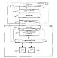
- FIG. 1shows the camera system as disclosed in US published application no. 2003/0193604;
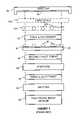
- FIG. 2shows a digital image acquisition device according to certain embodiments.
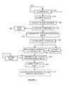
- FIG. 3shows a flow diagram illustrating the operation of the camera firmware.
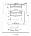
- FIG. 4shows a further digital image acquisition device according to certain embodiments.
- a digital image acquisition deviceis provided with an image acquisition sensor, preferably a CMOS or CCD array (herein generically referred to CCD), a shutter, an aperture and one or more optical elements for focusing an image on the sensor.
- the deviceincludes an internal light source, e.g., an LED or LED array, located in the body of the device, preferably between the sensor and the shutter.
- the deviceis arranged to activate the light source for a short period of time in accordance with a predefined criteria which can be either just before taking an image of a scene, or at any moment during inactivity of the device (in accordance with a predefined schedule), or just after each turn-ON of the device, or after a change of lens is detected or any combination of the criteria above, and to derive a map of defects on the surface of the sensor from a calibration image acquired by the sensor when illuminated by the light source.
- a predefined criteriacan be either just before taking an image of a scene, or at any moment during inactivity of the device (in accordance with a predefined schedule), or just after each turn-ON of the device, or after a change of lens is detected or any combination of the criteria above, and to derive a map of defects on the surface of the sensor from a calibration image acquired by the sensor when illuminated by the light source.
- An optical solutionis provided for automatically building a dust map in DSLR cameras.
- the deviceis arranged to automatically detect the need to re-calibrate the dust map by comparing different calibration images acquired by the sensor when lit by the light source.
- the obtained calibration imagewill be uniform enough to allow construction of a map of dust related defects on the CCD sensor surface. Even if the CCD surface is not uniformly lit (as a consequence of an off-center LED) the non-uniformity is persistent, and can be thus accounted for in a map or a formula that can be stored (in a compressed form) in a lookup table for mapping a calibration image to a final dust map.
- the optical elementsare part of a removable lens.
- an advantageous cameracan be arranged to receive multiple interchangeable lenses, which is cost effective. This was not considered by Robins in the 2003/0193604 application, which related to a digital camera with an integral lens.
- a technique in accordance with an embodimentmay be implemented automatically, whereas Robins requires the user to put the lens cover in place before calibration.
- a technique in accordance with another embodimentinvolves the formation of the calibration image directly from the light source, some of which may be obscured by dust or other defects.
- the calibration imageis obtained from rays that are reflected by lens contaminants.
- a technique in accordance with another embodimentcan work with both the aperture and the shutter closed, because in this embodiment, the light source disposed between the sensor and both the aperture and the shutter.
- both the aperture and the shuttermust be open to acquire the calibration image, because the aperture and shutter of Robins are located between the light source and sensor.
- Another embodimentincludes the light source not being focused using the optical system, such that the solution is not dependent on the optical nature of any lenses, and thus computational compensation for various zoom factors or lenses with different focal lengths is obviated.
- the LEDscan be placed within the camera body between the lens assembly and the shutter. In this case, the shutter is opened, even if not necessarily the aperture, when acquiring the calibration image for the dust map.
- the devicemay be programmed to activate an LED and capture an image only when the lens cap is on, such that no external light can diffuse the shadows created by the LED light.
- a dust detection algorithmcan be used to construct a dust map for the lens elements. So, for example, when an image of a scene is acquired, the CCD dust map can be used to correct CCD defects, and then a statistical dust map may be provided in accordance with PCT Application No. PCT/EP2004/010199 or US published application no. 2005/0078173, which are hereby incorporated by reference and assigned to the same assignee as the present application, can be used to correct for image defects caused by dust particles in the optical elements.
- Robinsdoes not disclose a technique for distinguishing between (a) image defects resulting from particles or imperfections on the sensor; and (b) lens element-related defects which ought to be treated differently, especially as the effect of the latter varies more greatly as image acquisition parameters such as focal length and aperture change.
- a calibration method in accordance with another embodimentcan also be used to detect defects in the sensor also known as “dead-pixels” and “burned pixels”.
- a small light source 210(e.g., a LED) is mounted within a camera body 200 between a CCD sensor 52 and a shutter 50 . Illumination of the light source 210 , and/or control of other aspects of camera functionality (not shown) is controlled by camera firmware 220 or other program media.
- the camera body 200receives an interchangeable lens 240 including lens elements 42 , 44 and 46 and aperture 48 , which may have similar in functionality to the corresponding elements of FIG. 1 , except that in Robins the lens is integral with the camera body.
- the camera firmware 220preferably controls the operation of the lens 240 including setting and reading image acquisition parameters including focal length and aperture as described elsewhere.
- the firmwareis arranged to periodically illuminate the light source 210 when the shutter 50 is closed, and to store a calibration image acquired by the sensor.
- the source light 210is not central with respect to the sensor 52 .
- the camera firmwareincludes a look-up table 250 specific to the camera model to provide a mapping from an acquired calibration image to the real dust position on the CCD sensor. This real dust position information is stored in a map 260 .
- the mappingshifts the calibration image in a direction towards the light source to compensate for non-uniform illumination of the sensor due to the fact that the light source 210 may not be central or uniform with respect to the sensor.
- a background or event driven processbegins during a camera idle period 300 , for example, just before taking an image of a scene, or at any moment during inactivity in accordance with a predefined schedule, or just after each turn-ON, or the process can run every N pictures, say for N between 3 and 10, or a combination of these or other events such as putting on a lens cap or turning the camera off or just after taking an image.
- the processthen causes the source 210 to illuminate the sensor 52 with the shutter closed 310 .
- a calibration imageis then acquired 320 and can either be stored in volatile or non-volatile memory for whatever predetermined duration.
- the calibration imagecan first be checked for an aggregate number of defects, and if these exceed a threshold, an alarm can be provided 340 to the user to service the camera body.
- the thresholdcan be based on a simple integral or average of image luminance or indeed a count of discrete defects. If an alarm is registered, the process can either continue or terminate.
- the calibration imagecan then be compared 350 , 360 with a previous calibration image, if available, to determine if greater than a significant degree of change has occurred. If not 370 , the process can terminate before running again at a later time/event.
- the calibration imageis mapped through the look-up table 250 to produce the dust map 260 .
- the mapping from the calibration image to the dust maptakes into account the difference in the effect of the light from the source 210 on sensor defects compared to the effect of light through the aperture 48 and shutter 50 on sensor defects when acquiring an image normally.
- the calibration image 250 and/or dust map 260can be processed either as a binary image, with defects either occluding the sensor or not, or as a gray scale or probabilistic type image according to the nature of image correction that may be performed later when processing/correcting normally acquired images using the dust map.
- the current dust map 260can be stored either in volatile or non-volatile memory, for later use in processing acquired images. If storage space is at a premium, the firmware can overwrite the calibration image 250 information with the dust map 260 .
- the cameracan acquire images as normal at 400 .
- the dust map 260 or a pointer to the dust mapcan be saved with each acquired image 410 .
- the mapcan be stored in a MakerNote exif tag.
- a pointer to a dust mapis useful where many acquired images may be associated with the same dust map. In such cases, several versions of dust maps may be stored with different acquired images including pointers to different maps.
- an imagecan be compared with the dust map 260 to identify and/or correct defects in the image resulting from sensor defects 420 .
- this processingis likely to be performed in the background during periods of camera inactivity.
- the dust mapcould be used both to analyze and correct low resolution preview or post-view images as well as full resolution acquired images.
- image processing software or firmwarecan then continue by using techniques disclosed in, for example, the PCT Application No. PCT/EP2004/010199, incorporated by reference above, to detect and correct at 430 for image defects resulting from dust artifacts in the image acquisition optics.
- the light source 210can emit in any region of the spectrum in which the CCD is sensitive, for example, infrared.
- many LEDs ( 230 )may be used to obtain a symmetrical illumination of the CCD, although some calibration may still be required in such cases to take into account the difference in such illumination from light through the aperture 48 and shutter 50 .
- the light source or sourcesmay move, e.g., with the closing of the shutter or with separate mechanics, from being out of the way for the device to take a picture to a position wherein a better calibration image may be taken.
Landscapes
- Engineering & Computer Science (AREA)
- Multimedia (AREA)
- Signal Processing (AREA)
- Quality & Reliability (AREA)
- Computer Vision & Pattern Recognition (AREA)
- Physics & Mathematics (AREA)
- General Physics & Mathematics (AREA)
- Theoretical Computer Science (AREA)
- Studio Devices (AREA)
- Facsimile Scanning Arrangements (AREA)
- Image Input (AREA)
- Investigating, Analyzing Materials By Fluorescence Or Luminescence (AREA)
Abstract
Description
Claims (53)
Priority Applications (7)
| Application Number | Priority Date | Filing Date | Title |
|---|---|---|---|
| PCT/US2007/062093WO2007095556A2 (en) | 2006-02-14 | 2007-02-13 | Digital image acquisition device with built in dust and sensor mapping capability |
| US11/674,650US7702236B2 (en) | 2006-02-14 | 2007-02-13 | Digital image acquisition device with built in dust and sensor mapping capability |
| US12/140,048US8682097B2 (en) | 2006-02-14 | 2008-06-16 | Digital image enhancement with reference images |
| US12/140,950US9129381B2 (en) | 2003-06-26 | 2008-06-17 | Modification of post-viewing parameters for digital images using image region or feature information |
| US12/755,097US20100194895A1 (en) | 2006-02-14 | 2010-04-06 | Digital Image Acquisition Device with Built in Dust and Sensor Mapping Capability |
| US14/846,390US9692964B2 (en) | 2003-06-26 | 2015-09-04 | Modification of post-viewing parameters for digital images using image region or feature information |
| US15/633,328US20180013950A1 (en) | 2003-06-26 | 2017-06-26 | Modification of post-viewing parameters for digital images using image region or feature information |
Applications Claiming Priority (2)
| Application Number | Priority Date | Filing Date | Title |
|---|---|---|---|
| US77371406P | 2006-02-14 | 2006-02-14 | |
| US11/674,650US7702236B2 (en) | 2006-02-14 | 2007-02-13 | Digital image acquisition device with built in dust and sensor mapping capability |
Related Parent Applications (1)
| Application Number | Title | Priority Date | Filing Date |
|---|---|---|---|
| US11/836,744Continuation-In-PartUS8073286B2 (en) | 2003-06-26 | 2007-08-09 | Detection and correction of flash artifacts from airborne particulates |
Related Child Applications (2)
| Application Number | Title | Priority Date | Filing Date |
|---|---|---|---|
| US12/140,048Continuation-In-PartUS8682097B2 (en) | 2003-06-26 | 2008-06-16 | Digital image enhancement with reference images |
| US12/755,097ContinuationUS20100194895A1 (en) | 2006-02-14 | 2010-04-06 | Digital Image Acquisition Device with Built in Dust and Sensor Mapping Capability |
Publications (2)
| Publication Number | Publication Date |
|---|---|
| US20070189757A1 US20070189757A1 (en) | 2007-08-16 |
| US7702236B2true US7702236B2 (en) | 2010-04-20 |
Family
ID=38368610
Family Applications (2)
| Application Number | Title | Priority Date | Filing Date |
|---|---|---|---|
| US11/674,650Active2027-07-29US7702236B2 (en) | 2003-06-26 | 2007-02-13 | Digital image acquisition device with built in dust and sensor mapping capability |
| US12/755,097AbandonedUS20100194895A1 (en) | 2006-02-14 | 2010-04-06 | Digital Image Acquisition Device with Built in Dust and Sensor Mapping Capability |
Family Applications After (1)
| Application Number | Title | Priority Date | Filing Date |
|---|---|---|---|
| US12/755,097AbandonedUS20100194895A1 (en) | 2006-02-14 | 2010-04-06 | Digital Image Acquisition Device with Built in Dust and Sensor Mapping Capability |
Country Status (2)
| Country | Link |
|---|---|
| US (2) | US7702236B2 (en) |
| WO (1) | WO2007095556A2 (en) |
Cited By (17)
| Publication number | Priority date | Publication date | Assignee | Title |
|---|---|---|---|---|
| US20100194402A1 (en)* | 2008-06-06 | 2010-08-05 | Globalfoundries Inc. | Operating characteristic measurement device and methods thereof |
| US20110216158A1 (en)* | 2010-03-05 | 2011-09-08 | Tessera Technologies Ireland Limited | Object Detection and Rendering for Wide Field of View (WFOV) Image Acquisition Systems |
| US8213737B2 (en) | 2007-06-21 | 2012-07-03 | DigitalOptics Corporation Europe Limited | Digital image enhancement with reference images |
| US8335355B2 (en) | 2004-12-29 | 2012-12-18 | DigitalOptics Corporation Europe Limited | Method and component for image recognition |
| US8503800B2 (en) | 2007-03-05 | 2013-08-06 | DigitalOptics Corporation Europe Limited | Illumination detection using classifier chains |
| KR20130098298A (en) | 2010-07-07 | 2013-09-04 | 디지털옵틱스 코포레이션 유럽 리미티드 | Real-time video frame pre-processing hardware |
| US8593542B2 (en) | 2005-12-27 | 2013-11-26 | DigitalOptics Corporation Europe Limited | Foreground/background separation using reference images |
| US8682097B2 (en) | 2006-02-14 | 2014-03-25 | DigitalOptics Corporation Europe Limited | Digital image enhancement with reference images |
| US8723959B2 (en) | 2011-03-31 | 2014-05-13 | DigitalOptics Corporation Europe Limited | Face and other object tracking in off-center peripheral regions for nonlinear lens geometries |
| US8860816B2 (en) | 2011-03-31 | 2014-10-14 | Fotonation Limited | Scene enhancements in off-center peripheral regions for nonlinear lens geometries |
| US8896703B2 (en) | 2011-03-31 | 2014-11-25 | Fotonation Limited | Superresolution enhancment of peripheral regions in nonlinear lens geometries |
| US8982180B2 (en) | 2011-03-31 | 2015-03-17 | Fotonation Limited | Face and other object detection and tracking in off-center peripheral regions for nonlinear lens geometries |
| US9298957B2 (en)* | 2014-07-31 | 2016-03-29 | Symbol Technologies, Llc | Detecting window deterioration on barcode scanning workstation |
| WO2019236953A1 (en)* | 2018-06-08 | 2019-12-12 | Storevision North America Inc. | A panoptes device or image acquisition system having multiple independent sensors |
| US20200213581A1 (en)* | 2018-12-27 | 2020-07-02 | Waymo Llc | Identifying Defects in Optical Detector Systems Based on Extent of Stray Light |
| US20220196626A1 (en)* | 2019-04-17 | 2022-06-23 | Hefei Midea Refrigerator Co., Ltd. | Water quality monitoring method for water supply system, water supply system, and refrigeration apparatus |
| US12175654B2 (en) | 2020-11-06 | 2024-12-24 | Carl Zeiss Metrology Llc | Surface inspection system and method for differentiating particulate contamination from defects on a surface of a specimen |
Families Citing this family (47)
| Publication number | Priority date | Publication date | Assignee | Title |
|---|---|---|---|---|
| US8948468B2 (en) | 2003-06-26 | 2015-02-03 | Fotonation Limited | Modification of viewing parameters for digital images using face detection information |
| US7440593B1 (en) | 2003-06-26 | 2008-10-21 | Fotonation Vision Limited | Method of improving orientation and color balance of digital images using face detection information |
| US7844076B2 (en) | 2003-06-26 | 2010-11-30 | Fotonation Vision Limited | Digital image processing using face detection and skin tone information |
| US7269292B2 (en) | 2003-06-26 | 2007-09-11 | Fotonation Vision Limited | Digital image adjustable compression and resolution using face detection information |
| US7471846B2 (en) | 2003-06-26 | 2008-12-30 | Fotonation Vision Limited | Perfecting the effect of flash within an image acquisition devices using face detection |
| US8330831B2 (en) | 2003-08-05 | 2012-12-11 | DigitalOptics Corporation Europe Limited | Method of gathering visual meta data using a reference image |
| US7616233B2 (en) | 2003-06-26 | 2009-11-10 | Fotonation Vision Limited | Perfecting of digital image capture parameters within acquisition devices using face detection |
| US8494286B2 (en) | 2008-02-05 | 2013-07-23 | DigitalOptics Corporation Europe Limited | Face detection in mid-shot digital images |
| US8498452B2 (en) | 2003-06-26 | 2013-07-30 | DigitalOptics Corporation Europe Limited | Digital image processing using face detection information |
| US9692964B2 (en) | 2003-06-26 | 2017-06-27 | Fotonation Limited | Modification of post-viewing parameters for digital images using image region or feature information |
| US8989453B2 (en) | 2003-06-26 | 2015-03-24 | Fotonation Limited | Digital image processing using face detection information |
| US7620218B2 (en) | 2006-08-11 | 2009-11-17 | Fotonation Ireland Limited | Real-time face tracking with reference images |
| US8155397B2 (en) | 2007-09-26 | 2012-04-10 | DigitalOptics Corporation Europe Limited | Face tracking in a camera processor |
| US7565030B2 (en) | 2003-06-26 | 2009-07-21 | Fotonation Vision Limited | Detecting orientation of digital images using face detection information |
| US9129381B2 (en) | 2003-06-26 | 2015-09-08 | Fotonation Limited | Modification of post-viewing parameters for digital images using image region or feature information |
| US7792970B2 (en) | 2005-06-17 | 2010-09-07 | Fotonation Vision Limited | Method for establishing a paired connection between media devices |
| US7574016B2 (en) | 2003-06-26 | 2009-08-11 | Fotonation Vision Limited | Digital image processing using face detection information |
| US7676110B2 (en)* | 2003-09-30 | 2010-03-09 | Fotonation Vision Limited | Determination of need to service a camera based on detection of blemishes in digital images |
| US7424170B2 (en) | 2003-09-30 | 2008-09-09 | Fotonation Vision Limited | Automated statistical self-calibrating detection and removal of blemishes in digital images based on determining probabilities based on image analysis of single images |
| US7590305B2 (en)* | 2003-09-30 | 2009-09-15 | Fotonation Vision Limited | Digital camera with built-in lens calibration table |
| US7340109B2 (en)* | 2003-09-30 | 2008-03-04 | Fotonation Vision Limited | Automated statistical self-calibrating detection and removal of blemishes in digital images dependent upon changes in extracted parameter values |
| US8369650B2 (en) | 2003-09-30 | 2013-02-05 | DigitalOptics Corporation Europe Limited | Image defect map creation using batches of digital images |
| US7369712B2 (en)* | 2003-09-30 | 2008-05-06 | Fotonation Vision Limited | Automated statistical self-calibrating detection and removal of blemishes in digital images based on multiple occurrences of dust in images |
| US7295233B2 (en)* | 2003-09-30 | 2007-11-13 | Fotonation Vision Limited | Detection and removal of blemishes in digital images utilizing original images of defocused scenes |
| US8320641B2 (en) | 2004-10-28 | 2012-11-27 | DigitalOptics Corporation Europe Limited | Method and apparatus for red-eye detection using preview or other reference images |
| US7315631B1 (en) | 2006-08-11 | 2008-01-01 | Fotonation Vision Limited | Real-time face tracking in a digital image acquisition device |
| WO2007095556A2 (en) | 2006-02-14 | 2007-08-23 | Fotonation Vision Limited | Digital image acquisition device with built in dust and sensor mapping capability |
| EP2033142B1 (en) | 2006-06-12 | 2011-01-26 | Tessera Technologies Ireland Limited | Advances in extending the aam techniques from grayscale to color images |
| US7612805B2 (en) | 2006-07-11 | 2009-11-03 | Neal Solomon | Digital imaging system and methods for selective image filtration |
| US7916897B2 (en) | 2006-08-11 | 2011-03-29 | Tessera Technologies Ireland Limited | Face tracking for controlling imaging parameters |
| US7403643B2 (en) | 2006-08-11 | 2008-07-22 | Fotonation Vision Limited | Real-time face tracking in a digital image acquisition device |
| US8055067B2 (en) | 2007-01-18 | 2011-11-08 | DigitalOptics Corporation Europe Limited | Color segmentation |
| JP5049356B2 (en) | 2007-02-28 | 2012-10-17 | デジタルオプティックス・コーポレイション・ヨーロッパ・リミテッド | Separation of directional lighting variability in statistical face modeling based on texture space decomposition |
| JP4970557B2 (en) | 2007-03-05 | 2012-07-11 | デジタルオプティックス・コーポレイション・ヨーロッパ・リミテッド | Face search and detection in digital image capture device |
| US7916971B2 (en) | 2007-05-24 | 2011-03-29 | Tessera Technologies Ireland Limited | Image processing method and apparatus |
| US7855737B2 (en) | 2008-03-26 | 2010-12-21 | Fotonation Ireland Limited | Method of making a digital camera image of a scene including the camera user |
| CN102027505A (en) | 2008-07-30 | 2011-04-20 | 泰塞拉技术爱尔兰公司 | Automatic face and skin retouching using face detection |
| CN101941012B (en)* | 2009-07-03 | 2012-04-25 | 泰怡凯电器(苏州)有限公司 | Cleaning robot, dirt recognition device thereof and cleaning method of cleaning robot |
| US8379917B2 (en) | 2009-10-02 | 2013-02-19 | DigitalOptics Corporation Europe Limited | Face recognition performance using additional image features |
| DE102009049203B4 (en)* | 2009-10-13 | 2016-10-13 | Arnold & Richter Cine Technik Gmbh & Co. Betriebs Kg | Diagnostic unit for an electronic camera and camera system |
| JP2012037574A (en)* | 2010-08-03 | 2012-02-23 | Olympus Imaging Corp | Electronic imaging apparatus |
| DE102010041447A1 (en)* | 2010-09-27 | 2012-03-29 | Robert Bosch Gmbh | Method for Authenticating a Charge Coupled Device (CCD) |
| US9136185B2 (en)* | 2011-12-19 | 2015-09-15 | MEMC Singapore Pte., Ltd. | Methods and systems for grain size evaluation of multi-cystalline solar wafers |
| JP6376934B2 (en) | 2014-10-14 | 2018-08-22 | シャープ株式会社 | Image processing apparatus, imaging apparatus, image processing method, and program |
| RU2682012C1 (en)* | 2018-05-04 | 2019-03-14 | Закрытое акционерное общество "МНИТИ" (ЗАО "МНИТИ") | Device for identifying electronic portrait of thermal imaging camera |
| WO2019216578A1 (en)* | 2018-05-11 | 2019-11-14 | Samsung Electronics Co., Ltd. | Method and apparatus for executing cleaning operation |
| DE102019128503A1 (en)* | 2019-10-22 | 2021-04-22 | Krones Aktiengesellschaft | Method and device for the optical inspection of containers |
Citations (110)
| Publication number | Priority date | Publication date | Assignee | Title |
|---|---|---|---|---|
| US3541941A (en) | 1967-08-07 | 1970-11-24 | Rank Organisation Ltd | Camera systems |
| US3621136A (en) | 1969-09-10 | 1971-11-16 | Us Navy | Automatic optical-focusing system for tv cameras |
| US4186301A (en) | 1977-04-05 | 1980-01-29 | Commissariat A L'energie Atomique | Automatic focus control for a microscope |
| US4354204A (en) | 1980-02-18 | 1982-10-12 | Kenji Kimura | Automatic focusing control device |
| US4748509A (en) | 1986-09-18 | 1988-05-31 | Victor Company Of Japan, Ltd. | Focusing control and indication of information relating to an object |
| US5065257A (en) | 1985-03-20 | 1991-11-12 | Canon Kabushiki Kaisha | Image processing apparatus with means for compensating for dust., etc., on an original |
| US5093716A (en) | 1990-02-15 | 1992-03-03 | Sony Corporation | Digital color video camera with auto-focus, auto-exposure and auto-white balance, and an auto exposure system therefor which compensates for abnormal lighting |
| US5214470A (en) | 1992-04-09 | 1993-05-25 | Xerox Corporation | Method and apparatus for compensating for dirt or etched areas on a document platen |
| US5216504A (en) | 1991-09-25 | 1993-06-01 | Display Laboratories, Inc. | Automatic precision video monitor alignment system |
| US5315538A (en) | 1992-03-23 | 1994-05-24 | Hughes Aircraft Company | Signal processing incorporating signal, tracking, estimation, and removal processes using a maximum a posteriori algorithm, and sequential signal detection |
| US5416516A (en) | 1992-03-16 | 1995-05-16 | Sony Corporation | Solid-state image pickup apparatus having a defect detecting mode |
| US5436979A (en) | 1992-08-21 | 1995-07-25 | Eastman Kodak Company | Process for detecting and mapping dirt on the surface of a photographic element |
| US5475429A (en) | 1991-07-25 | 1995-12-12 | Olympus Optical Co., Ltd. | In-focus sensing device for sensing an in-focus condition using a ratio of frequency components at different positions |
| US5485534A (en) | 1990-03-28 | 1996-01-16 | Fuji Photo Film Co., Ltd. | Method and apparatus for emphasizing sharpness of image by detecting the edge portions of the image |
| US5526446A (en) | 1991-09-24 | 1996-06-11 | Massachusetts Institute Of Technology | Noise reduction system |
| US5541655A (en) | 1991-11-05 | 1996-07-30 | Canon Kabushiki Kaisha | Image pickup device |
| US5557689A (en) | 1991-11-19 | 1996-09-17 | Xerox Corporation | Optical word recognition by examination of word shape |
| US5576715A (en) | 1994-03-07 | 1996-11-19 | Leica, Inc. | Method and apparatus for digital processing in a global positioning system receiver |
| US5625413A (en) | 1993-06-02 | 1997-04-29 | Hitachi, Ltd. | Video camera with a function to correct defective pixels of solid state image pickup device and method of correcting defective pixels of solid state image |
| US5643699A (en) | 1994-05-13 | 1997-07-01 | Waldner; Paul R. | Method and device for the mutual alignment of a film and a printed circuit board |
| US5873830A (en) | 1997-08-22 | 1999-02-23 | Acuson Corporation | Ultrasound imaging system and method for improving resolution and operation |
| US5926212A (en) | 1995-08-30 | 1999-07-20 | Sony Corporation | Image signal processing apparatus and recording/reproducing apparatus |
| US5926291A (en) | 1996-02-29 | 1999-07-20 | Konica Corporation | Method of calculating color correcting condition and medium for storing the method |
| US5965896A (en) | 1997-02-26 | 1999-10-12 | Marton & Associates, Inc. | Apparatus and method for scratch wear testing of thin films |
| US5969372A (en) | 1997-10-14 | 1999-10-19 | Hewlett-Packard Company | Film scanner with dust and scratch correction by use of dark-field illumination |
| US5974194A (en) | 1995-10-30 | 1999-10-26 | Sony Corporation | Projection based method for scratch and wire removal from digital images |
| US5982941A (en) | 1997-02-07 | 1999-11-09 | Eastman Kodak Company | Method of producing digital image with improved performance characteristic |
| US6002436A (en) | 1997-08-28 | 1999-12-14 | Flashpoint Technology, Inc. | Method and system for auto wake-up for time lapse image capture in an image capture unit |
| US6018363A (en) | 1994-04-28 | 2000-01-25 | Canon Kabushiki Kaisha | Image sensing apparatus with optical-axis deflecting device |
| US6035072A (en) | 1997-12-08 | 2000-03-07 | Read; Robert Lee | Mapping defects or dirt dynamically affecting an image acquisition device |
| US6035073A (en) | 1996-03-13 | 2000-03-07 | Siemens Aktiengesellschaft | Method for forming an image transformation matrix for an arbitrarily shaped image segment of a digital image with a computer |
| US6061092A (en) | 1997-12-05 | 2000-05-09 | Intel Corporation | Method and apparatus for dark frame cancellation for CMOS sensor-based tethered video peripherals |
| US6094511A (en) | 1996-07-31 | 2000-07-25 | Canon Kabushiki Kaisha | Image filtering method and apparatus with interpolation according to mapping function to produce final image |
| US6097847A (en) | 1993-05-31 | 2000-08-01 | Nec Corporation | Method of and apparatus for calculating sharpness of image and apparatus for sharpening image |
| US6125213A (en) | 1997-02-17 | 2000-09-26 | Canon Kabushiki Kaisha | Image processing method, an image processing apparatus, and a storage medium readable by a computer |
| US6139202A (en)* | 1998-12-08 | 2000-10-31 | Eastman Kodak Company | Aperture/shutter system with a motor component |
| US6167206A (en) | 1995-09-12 | 2000-12-26 | Smartlens Corporation | Image modifiers for use in photography |
| US6181378B1 (en) | 1996-06-14 | 2001-01-30 | Asahi Kogaku Kogyo Kabushiki Kaisha | Image reading device |
| US6192161B1 (en) | 1999-02-12 | 2001-02-20 | Sony Corporation | Method and apparatus for adaptive filter tap selection according to a class |
| US6233364B1 (en) | 1998-09-18 | 2001-05-15 | Dainippon Screen Engineering Of America Incorporated | Method and system for detecting and tagging dust and scratches in a digital image |
| US6231185B1 (en) | 1997-07-09 | 2001-05-15 | Siemens Aktiengesellschaft | Process and device for detecting a reflecting surface of a human being |
| US6266054B1 (en) | 1997-11-05 | 2001-07-24 | Microsoft Corporation | Automated removal of narrow, elongated distortions from a digital image |
| US20010039804A1 (en) | 1995-09-01 | 2001-11-15 | Nartron Corporation | Ice making system, method, and component apparatus |
| US6323855B1 (en) | 1998-12-10 | 2001-11-27 | Eastman Kodak Company | Sharpening edge features in digital image providing high frequency edge enhancement |
| EP1157544A1 (en) | 1999-02-26 | 2001-11-28 | Intel Corporation | Hi-speed deterministic approach in detecting defective pixels within an image sensor |
| US6326998B1 (en) | 1997-10-08 | 2001-12-04 | Eastman Kodak Company | Optical blur filter having a four-feature pattern |
| US6329826B1 (en) | 1996-03-05 | 2001-12-11 | Hitachi, Ltd. | Method and apparatus for inspecting integrated circuit pattern |
| US6344640B1 (en) | 1993-03-01 | 2002-02-05 | Geoffrey B. Rhoads | Method for wide field distortion-compensated imaging |
| EP1188309A1 (en) | 1999-05-21 | 2002-03-20 | Foveon, Inc. | Targetable autofocus system |
| US6364835B1 (en) | 1998-11-20 | 2002-04-02 | Acuson Corporation | Medical diagnostic ultrasound imaging methods for extended field of view |
| US6434272B1 (en) | 1996-12-18 | 2002-08-13 | Teknillinen Korkeakoulu, Viestintarekniiken Laboratorio | System and method for image processing |
| US6465801B1 (en) | 2000-07-31 | 2002-10-15 | Hewlett-Packard Company | Dust and scratch detection for an image scanner |
| US6487321B1 (en) | 1999-09-16 | 2002-11-26 | Applied Science Fiction | Method and system for altering defects in a digital image |
| US20030036860A1 (en) | 2001-06-20 | 2003-02-20 | Xenogen Corporation | Absolute intensity determination for a light source in low level light imaging systems |
| US20030039402A1 (en)* | 2001-08-24 | 2003-02-27 | Robins David R. | Method and apparatus for detection and removal of scanned image scratches and dust |
| US6563945B2 (en) | 1997-03-24 | 2003-05-13 | Jack M. Holm | Pictorial digital image processing incorporating image and output device modifications |
| US6567116B1 (en) | 1998-11-20 | 2003-05-20 | James A. Aman | Multiple object tracking system |
| US6587592B2 (en) | 2001-11-16 | 2003-07-01 | Adobe Systems Incorporated | Generating replacement data values for an image region |
| US20030174902A1 (en) | 2002-03-18 | 2003-09-18 | Creo Il Ltd. | Method and apparatus for capturing images using blemished sensors |
| US20030193604A1 (en) | 2002-04-11 | 2003-10-16 | Robins Mark Nelson | Camera lens contamination detection and indication system and method |
| US6636646B1 (en) | 2000-07-20 | 2003-10-21 | Eastman Kodak Company | Digital image processing method and for brightness adjustment of digital images |
| US6690816B2 (en) | 2000-04-07 | 2004-02-10 | The University Of North Carolina At Chapel Hill | Systems and methods for tubular object processing |
| US6700667B2 (en) | 1996-10-21 | 2004-03-02 | Nikon Corporation | Exposure apparatus and method |
| US6707950B1 (en) | 1999-06-22 | 2004-03-16 | Eastman Kodak Company | Method for modification of non-image data in an image processing chain |
| US6733136B2 (en) | 2001-06-06 | 2004-05-11 | Spitz, Inc. | Video-based immersive theater |
| US6740883B1 (en) | 1998-08-14 | 2004-05-25 | Robert Z. Stodilka | Application of scatter and attenuation correction to emission tomography images using inferred anatomy from atlas |
| US6792161B1 (en) | 1998-07-31 | 2004-09-14 | Minolta Co., Ltd. | Image input device with dust detector |
| US6791608B1 (en) | 1999-02-24 | 2004-09-14 | Olympus Optical Co., Ltd. | Digital camera and dirt position detecting method for digital camera |
| EP1478169A2 (en) | 2003-05-16 | 2004-11-17 | Nikon Corporation | Image-capturing apparatus and image processing apparatus |
| JP2004327485A (en)* | 2003-04-21 | 2004-11-18 | Canon Inc | Method for removing foreign matter from exposure mask |
| US6829008B1 (en) | 1998-08-20 | 2004-12-07 | Canon Kabushiki Kaisha | Solid-state image sensing apparatus, control method therefor, image sensing apparatus, basic layout of photoelectric conversion cell, and storage medium |
| US6842196B1 (en) | 2000-04-04 | 2005-01-11 | Smith & Nephew, Inc. | Method and system for automatic correction of motion artifacts |
| EP1507157A2 (en) | 2002-04-05 | 2005-02-16 | Canon Kabushiki Kaisha | Image pickup apparatus with a focus adjusting device and an exposure system |
| US20050068450A1 (en) | 2003-09-30 | 2005-03-31 | Eran Steinberg | Automated statistical self-calibrating detection and removal of blemishes in digital images dependent upon changes in extracted parameter values |
| US20050068449A1 (en) | 2003-09-30 | 2005-03-31 | Eran Steinberg | Automated statistical self-calibrating detection and removal of blemishes in digital images based on a dust map developed from actual image data |
| US20050068445A1 (en) | 2003-09-30 | 2005-03-31 | Eran Steinberg | Digital camera |
| US20050068446A1 (en) | 2003-09-30 | 2005-03-31 | Eran Steinberg | Automated statistical self-calibrating detection and removal of blemishes in digital images based on multiple occurrences of dust in images |
| US20050068447A1 (en) | 2003-09-30 | 2005-03-31 | Eran Steinberg | Digital image acquisition and processing system |
| US20050068452A1 (en)* | 2003-09-30 | 2005-03-31 | Eran Steinberg | Digital camera with built-in lens calibration table |
| US20050068448A1 (en) | 2003-09-30 | 2005-03-31 | Eran Steinberg | Method of detecting and correcting dust in digital images based on aura and shadow region analysis |
| US20050068451A1 (en) | 2003-09-30 | 2005-03-31 | Eran Steinberg | Automated statistical self-calibrating detection and removal of blemishes in digital images based on determining probabilities based on image analysis of single images |
| US6874420B2 (en) | 1999-10-22 | 2005-04-05 | Cc1, Inc. | System and method for register mark recognition |
| US20050078173A1 (en) | 2003-09-30 | 2005-04-14 | Eran Steinberg | Determination of need to service a camera based on detection of blemishes in digital images |
| WO2005041558A1 (en) | 2003-09-30 | 2005-05-06 | Fotonation Vision Limited | Statistical self-calibrating detection and removal of blemishes in digital images |
| US6895109B1 (en) | 1997-09-04 | 2005-05-17 | Texas Instruments Incorporated | Apparatus and method for automatically detecting defects on silicon dies on silicon wafers |
| US20050104997A1 (en) | 2003-11-17 | 2005-05-19 | Osamu Nonaka | Lens replacement type imaging apparatus, control apparatus, cleaning apparatus, and cleaning method |
| US6919892B1 (en) | 2002-08-14 | 2005-07-19 | Avaworks, Incorporated | Photo realistic talking head creation system and method |
| US6933978B1 (en) | 1999-10-28 | 2005-08-23 | Canon Kabushiki Kaisha | Focus detecting device with photoelectric conversion portion having microlens and with light blocking portion having first and second openings |
| US6940550B2 (en) | 2001-01-12 | 2005-09-06 | Fuji Photo Film Co., Ltd. | Digital camera and a method for correcting dust images in the camera |
| US6940545B1 (en) | 2000-02-28 | 2005-09-06 | Eastman Kodak Company | Face detecting camera and method |
| US6947786B2 (en) | 2002-02-28 | 2005-09-20 | Surgical Navigation Technologies, Inc. | Method and apparatus for perspective inversion |
| US6983886B2 (en) | 2002-07-19 | 2006-01-10 | Keyence Corporation | Two-dimensional code reader setting method, two-dimensional code reader, two dimensional code reader setting program and computer readable recording medium |
| US6995346B2 (en) | 2002-12-11 | 2006-02-07 | Dialog Semiconductor Gmbh | Fixed pattern noise compensation with low memory requirements |
| US7003136B1 (en) | 2002-04-26 | 2006-02-21 | Hewlett-Packard Development Company, L.P. | Plan-view projections of depth image data for object tracking |
| US20060039690A1 (en) | 2004-08-16 | 2006-02-23 | Eran Steinberg | Foreground/background segmentation in digital images with differential exposure calculations |
| US7020350B2 (en) | 2000-06-15 | 2006-03-28 | Hitachi, Ltd. | Image alignment method, comparative inspection method, and comparative inspection device for comparative inspections |
| US20060098237A1 (en) | 2004-11-10 | 2006-05-11 | Eran Steinberg | Method and apparatus for initiating subsequent exposures based on determination of motion blurring artifacts |
| US20060098890A1 (en) | 2004-11-10 | 2006-05-11 | Eran Steinberg | Method of determining PSF using multiple instances of a nominally similar scene |
| US20060098891A1 (en) | 2004-11-10 | 2006-05-11 | Eran Steinberg | Method of notifying users regarding motion artifacts based on image analysis |
| US7058294B2 (en) | 2003-04-08 | 2006-06-06 | Pentax Corporation | Passive autofocus system for a camera |
| US7061648B2 (en) | 2001-01-17 | 2006-06-13 | Canon Kabushiki Kaisha | Calibration method for density in image forming apparatus |
| US7085430B2 (en) | 2001-11-23 | 2006-08-01 | Imaging Dynamics Company Ltd. | Correcting geometric distortion in a digitally captured image |
| US7149262B1 (en) | 2000-07-06 | 2006-12-12 | The Trustees Of Columbia University In The City Of New York | Method and apparatus for enhancing data resolution |
| US20070116380A1 (en) | 2005-11-18 | 2007-05-24 | Mihai Ciuc | Method and apparatus of correcting hybrid flash artifacts in digital images |
| US7245315B2 (en) | 2002-05-20 | 2007-07-17 | Simmonds Precision Products, Inc. | Distinguishing between fire and non-fire conditions using cameras |
| US7256818B2 (en) | 2002-05-20 | 2007-08-14 | Simmonds Precision Products, Inc. | Detecting fire using cameras |
| WO2007095483A2 (en) | 2006-02-14 | 2007-08-23 | Fotonation Vision Limited | Detection and removal of blemishes in digital images utilizing original images of defocused scenes |
| WO2007095556A2 (en) | 2006-02-14 | 2007-08-23 | Fotonation Vision Limited | Digital image acquisition device with built in dust and sensor mapping capability |
| US7280696B2 (en) | 2002-05-20 | 2007-10-09 | Simmonds Precision Products, Inc. | Video detection/verification system |
| US20080240555A1 (en) | 2005-11-18 | 2008-10-02 | Florin Nanu | Two Stage Detection for Photographic Eye Artifacts |
Family Cites Families (1)
| Publication number | Priority date | Publication date | Assignee | Title |
|---|---|---|---|---|
| US6704458B2 (en)* | 1999-12-29 | 2004-03-09 | Eastman Kodak Company | Method and apparatus for correcting heavily damaged images |
- 2007
- 2007-02-13WOPCT/US2007/062093patent/WO2007095556A2/enactiveApplication Filing
- 2007-02-13USUS11/674,650patent/US7702236B2/enactiveActive
- 2010
- 2010-04-06USUS12/755,097patent/US20100194895A1/ennot_activeAbandoned
Patent Citations (126)
| Publication number | Priority date | Publication date | Assignee | Title |
|---|---|---|---|---|
| US3541941A (en) | 1967-08-07 | 1970-11-24 | Rank Organisation Ltd | Camera systems |
| US3621136A (en) | 1969-09-10 | 1971-11-16 | Us Navy | Automatic optical-focusing system for tv cameras |
| US4186301A (en) | 1977-04-05 | 1980-01-29 | Commissariat A L'energie Atomique | Automatic focus control for a microscope |
| US4354204A (en) | 1980-02-18 | 1982-10-12 | Kenji Kimura | Automatic focusing control device |
| US5065257A (en) | 1985-03-20 | 1991-11-12 | Canon Kabushiki Kaisha | Image processing apparatus with means for compensating for dust., etc., on an original |
| US4748509A (en) | 1986-09-18 | 1988-05-31 | Victor Company Of Japan, Ltd. | Focusing control and indication of information relating to an object |
| US5093716A (en) | 1990-02-15 | 1992-03-03 | Sony Corporation | Digital color video camera with auto-focus, auto-exposure and auto-white balance, and an auto exposure system therefor which compensates for abnormal lighting |
| US5485534A (en) | 1990-03-28 | 1996-01-16 | Fuji Photo Film Co., Ltd. | Method and apparatus for emphasizing sharpness of image by detecting the edge portions of the image |
| US5475429A (en) | 1991-07-25 | 1995-12-12 | Olympus Optical Co., Ltd. | In-focus sensing device for sensing an in-focus condition using a ratio of frequency components at different positions |
| US5526446A (en) | 1991-09-24 | 1996-06-11 | Massachusetts Institute Of Technology | Noise reduction system |
| US5216504A (en) | 1991-09-25 | 1993-06-01 | Display Laboratories, Inc. | Automatic precision video monitor alignment system |
| US5541655A (en) | 1991-11-05 | 1996-07-30 | Canon Kabushiki Kaisha | Image pickup device |
| US5557689A (en) | 1991-11-19 | 1996-09-17 | Xerox Corporation | Optical word recognition by examination of word shape |
| US5416516A (en) | 1992-03-16 | 1995-05-16 | Sony Corporation | Solid-state image pickup apparatus having a defect detecting mode |
| US5315538A (en) | 1992-03-23 | 1994-05-24 | Hughes Aircraft Company | Signal processing incorporating signal, tracking, estimation, and removal processes using a maximum a posteriori algorithm, and sequential signal detection |
| US5214470A (en) | 1992-04-09 | 1993-05-25 | Xerox Corporation | Method and apparatus for compensating for dirt or etched areas on a document platen |
| US5436979A (en) | 1992-08-21 | 1995-07-25 | Eastman Kodak Company | Process for detecting and mapping dirt on the surface of a photographic element |
| US6344640B1 (en) | 1993-03-01 | 2002-02-05 | Geoffrey B. Rhoads | Method for wide field distortion-compensated imaging |
| US6097847A (en) | 1993-05-31 | 2000-08-01 | Nec Corporation | Method of and apparatus for calculating sharpness of image and apparatus for sharpening image |
| US5625413A (en) | 1993-06-02 | 1997-04-29 | Hitachi, Ltd. | Video camera with a function to correct defective pixels of solid state image pickup device and method of correcting defective pixels of solid state image |
| US5576715A (en) | 1994-03-07 | 1996-11-19 | Leica, Inc. | Method and apparatus for digital processing in a global positioning system receiver |
| US6018363A (en) | 1994-04-28 | 2000-01-25 | Canon Kabushiki Kaisha | Image sensing apparatus with optical-axis deflecting device |
| US5643699A (en) | 1994-05-13 | 1997-07-01 | Waldner; Paul R. | Method and device for the mutual alignment of a film and a printed circuit board |
| US5926212A (en) | 1995-08-30 | 1999-07-20 | Sony Corporation | Image signal processing apparatus and recording/reproducing apparatus |
| US20010039804A1 (en) | 1995-09-01 | 2001-11-15 | Nartron Corporation | Ice making system, method, and component apparatus |
| US6167206A (en) | 1995-09-12 | 2000-12-26 | Smartlens Corporation | Image modifiers for use in photography |
| US5974194A (en) | 1995-10-30 | 1999-10-26 | Sony Corporation | Projection based method for scratch and wire removal from digital images |
| US5926291A (en) | 1996-02-29 | 1999-07-20 | Konica Corporation | Method of calculating color correcting condition and medium for storing the method |
| US7026830B2 (en) | 1996-03-05 | 2006-04-11 | Hitachi, Ltd. | Method and apparatus for inspecting integrated circuit pattern |
| US6329826B1 (en) | 1996-03-05 | 2001-12-11 | Hitachi, Ltd. | Method and apparatus for inspecting integrated circuit pattern |
| US6035073A (en) | 1996-03-13 | 2000-03-07 | Siemens Aktiengesellschaft | Method for forming an image transformation matrix for an arbitrarily shaped image segment of a digital image with a computer |
| US6181378B1 (en) | 1996-06-14 | 2001-01-30 | Asahi Kogaku Kogyo Kabushiki Kaisha | Image reading device |
| US6094511A (en) | 1996-07-31 | 2000-07-25 | Canon Kabushiki Kaisha | Image filtering method and apparatus with interpolation according to mapping function to produce final image |
| US6700667B2 (en) | 1996-10-21 | 2004-03-02 | Nikon Corporation | Exposure apparatus and method |
| US6434272B1 (en) | 1996-12-18 | 2002-08-13 | Teknillinen Korkeakoulu, Viestintarekniiken Laboratorio | System and method for image processing |
| US5982941A (en) | 1997-02-07 | 1999-11-09 | Eastman Kodak Company | Method of producing digital image with improved performance characteristic |
| US6125213A (en) | 1997-02-17 | 2000-09-26 | Canon Kabushiki Kaisha | Image processing method, an image processing apparatus, and a storage medium readable by a computer |
| US5965896A (en) | 1997-02-26 | 1999-10-12 | Marton & Associates, Inc. | Apparatus and method for scratch wear testing of thin films |
| US6563945B2 (en) | 1997-03-24 | 2003-05-13 | Jack M. Holm | Pictorial digital image processing incorporating image and output device modifications |
| US6231185B1 (en) | 1997-07-09 | 2001-05-15 | Siemens Aktiengesellschaft | Process and device for detecting a reflecting surface of a human being |
| US5873830A (en) | 1997-08-22 | 1999-02-23 | Acuson Corporation | Ultrasound imaging system and method for improving resolution and operation |
| US6002436A (en) | 1997-08-28 | 1999-12-14 | Flashpoint Technology, Inc. | Method and system for auto wake-up for time lapse image capture in an image capture unit |
| US6895109B1 (en) | 1997-09-04 | 2005-05-17 | Texas Instruments Incorporated | Apparatus and method for automatically detecting defects on silicon dies on silicon wafers |
| US6326998B1 (en) | 1997-10-08 | 2001-12-04 | Eastman Kodak Company | Optical blur filter having a four-feature pattern |
| US5969372A (en) | 1997-10-14 | 1999-10-19 | Hewlett-Packard Company | Film scanner with dust and scratch correction by use of dark-field illumination |
| US6266054B1 (en) | 1997-11-05 | 2001-07-24 | Microsoft Corporation | Automated removal of narrow, elongated distortions from a digital image |
| US6061092A (en) | 1997-12-05 | 2000-05-09 | Intel Corporation | Method and apparatus for dark frame cancellation for CMOS sensor-based tethered video peripherals |
| US6035072A (en) | 1997-12-08 | 2000-03-07 | Read; Robert Lee | Mapping defects or dirt dynamically affecting an image acquisition device |
| US6792161B1 (en) | 1998-07-31 | 2004-09-14 | Minolta Co., Ltd. | Image input device with dust detector |
| US6740883B1 (en) | 1998-08-14 | 2004-05-25 | Robert Z. Stodilka | Application of scatter and attenuation correction to emission tomography images using inferred anatomy from atlas |
| US6829008B1 (en) | 1998-08-20 | 2004-12-07 | Canon Kabushiki Kaisha | Solid-state image sensing apparatus, control method therefor, image sensing apparatus, basic layout of photoelectric conversion cell, and storage medium |
| US6233364B1 (en) | 1998-09-18 | 2001-05-15 | Dainippon Screen Engineering Of America Incorporated | Method and system for detecting and tagging dust and scratches in a digital image |
| US6364835B1 (en) | 1998-11-20 | 2002-04-02 | Acuson Corporation | Medical diagnostic ultrasound imaging methods for extended field of view |
| US6567116B1 (en) | 1998-11-20 | 2003-05-20 | James A. Aman | Multiple object tracking system |
| US6139202A (en)* | 1998-12-08 | 2000-10-31 | Eastman Kodak Company | Aperture/shutter system with a motor component |
| US6323855B1 (en) | 1998-12-10 | 2001-11-27 | Eastman Kodak Company | Sharpening edge features in digital image providing high frequency edge enhancement |
| US6192161B1 (en) | 1999-02-12 | 2001-02-20 | Sony Corporation | Method and apparatus for adaptive filter tap selection according to a class |
| US6791608B1 (en) | 1999-02-24 | 2004-09-14 | Olympus Optical Co., Ltd. | Digital camera and dirt position detecting method for digital camera |
| US6381357B1 (en) | 1999-02-26 | 2002-04-30 | Intel Corporation | Hi-speed deterministic approach in detecting defective pixels within an image sensor |
| EP1157544A1 (en) | 1999-02-26 | 2001-11-28 | Intel Corporation | Hi-speed deterministic approach in detecting defective pixels within an image sensor |
| EP1188309A1 (en) | 1999-05-21 | 2002-03-20 | Foveon, Inc. | Targetable autofocus system |
| US6707950B1 (en) | 1999-06-22 | 2004-03-16 | Eastman Kodak Company | Method for modification of non-image data in an image processing chain |
| US6487321B1 (en) | 1999-09-16 | 2002-11-26 | Applied Science Fiction | Method and system for altering defects in a digital image |
| US6874420B2 (en) | 1999-10-22 | 2005-04-05 | Cc1, Inc. | System and method for register mark recognition |
| US6933978B1 (en) | 1999-10-28 | 2005-08-23 | Canon Kabushiki Kaisha | Focus detecting device with photoelectric conversion portion having microlens and with light blocking portion having first and second openings |
| US6940545B1 (en) | 2000-02-28 | 2005-09-06 | Eastman Kodak Company | Face detecting camera and method |
| US6842196B1 (en) | 2000-04-04 | 2005-01-11 | Smith & Nephew, Inc. | Method and system for automatic correction of motion artifacts |
| US6690816B2 (en) | 2000-04-07 | 2004-02-10 | The University Of North Carolina At Chapel Hill | Systems and methods for tubular object processing |
| US7020350B2 (en) | 2000-06-15 | 2006-03-28 | Hitachi, Ltd. | Image alignment method, comparative inspection method, and comparative inspection device for comparative inspections |
| US7127126B2 (en) | 2000-06-15 | 2006-10-24 | Hitachi, Ltd. | Image alignment method, comparative inspection method, and comparative inspection device for comparative inspections |
| US7149262B1 (en) | 2000-07-06 | 2006-12-12 | The Trustees Of Columbia University In The City Of New York | Method and apparatus for enhancing data resolution |
| US6636646B1 (en) | 2000-07-20 | 2003-10-21 | Eastman Kodak Company | Digital image processing method and for brightness adjustment of digital images |
| US6465801B1 (en) | 2000-07-31 | 2002-10-15 | Hewlett-Packard Company | Dust and scratch detection for an image scanner |
| US6940550B2 (en) | 2001-01-12 | 2005-09-06 | Fuji Photo Film Co., Ltd. | Digital camera and a method for correcting dust images in the camera |
| US7061648B2 (en) | 2001-01-17 | 2006-06-13 | Canon Kabushiki Kaisha | Calibration method for density in image forming apparatus |
| US6733136B2 (en) | 2001-06-06 | 2004-05-11 | Spitz, Inc. | Video-based immersive theater |
| US20030036860A1 (en) | 2001-06-20 | 2003-02-20 | Xenogen Corporation | Absolute intensity determination for a light source in low level light imaging systems |
| US20030039402A1 (en)* | 2001-08-24 | 2003-02-27 | Robins David R. | Method and apparatus for detection and removal of scanned image scratches and dust |
| US6587592B2 (en) | 2001-11-16 | 2003-07-01 | Adobe Systems Incorporated | Generating replacement data values for an image region |
| US7085430B2 (en) | 2001-11-23 | 2006-08-01 | Imaging Dynamics Company Ltd. | Correcting geometric distortion in a digitally captured image |
| US6947786B2 (en) | 2002-02-28 | 2005-09-20 | Surgical Navigation Technologies, Inc. | Method and apparatus for perspective inversion |
| US20030174902A1 (en) | 2002-03-18 | 2003-09-18 | Creo Il Ltd. | Method and apparatus for capturing images using blemished sensors |
| EP1507157A2 (en) | 2002-04-05 | 2005-02-16 | Canon Kabushiki Kaisha | Image pickup apparatus with a focus adjusting device and an exposure system |
| EP1507157B1 (en) | 2002-04-05 | 2006-07-26 | Canon Kabushiki Kaisha | Image pickup apparatus with a focus adjusting device and an exposure system |
| US20030193604A1 (en) | 2002-04-11 | 2003-10-16 | Robins Mark Nelson | Camera lens contamination detection and indication system and method |
| US6940554B2 (en) | 2002-04-11 | 2005-09-06 | Hewlett-Packard Development Company, L.P. | Camera lens contamination detection and indication system and method |
| US7003136B1 (en) | 2002-04-26 | 2006-02-21 | Hewlett-Packard Development Company, L.P. | Plan-view projections of depth image data for object tracking |
| US7245315B2 (en) | 2002-05-20 | 2007-07-17 | Simmonds Precision Products, Inc. | Distinguishing between fire and non-fire conditions using cameras |
| US7280696B2 (en) | 2002-05-20 | 2007-10-09 | Simmonds Precision Products, Inc. | Video detection/verification system |
| US7256818B2 (en) | 2002-05-20 | 2007-08-14 | Simmonds Precision Products, Inc. | Detecting fire using cameras |
| US6983886B2 (en) | 2002-07-19 | 2006-01-10 | Keyence Corporation | Two-dimensional code reader setting method, two-dimensional code reader, two dimensional code reader setting program and computer readable recording medium |
| US6919892B1 (en) | 2002-08-14 | 2005-07-19 | Avaworks, Incorporated | Photo realistic talking head creation system and method |
| US6995346B2 (en) | 2002-12-11 | 2006-02-07 | Dialog Semiconductor Gmbh | Fixed pattern noise compensation with low memory requirements |
| US7058294B2 (en) | 2003-04-08 | 2006-06-06 | Pentax Corporation | Passive autofocus system for a camera |
| JP2004327485A (en)* | 2003-04-21 | 2004-11-18 | Canon Inc | Method for removing foreign matter from exposure mask |
| EP1478169A3 (en) | 2003-05-16 | 2006-03-22 | Nikon Corporation | Image-capturing apparatus and image processing apparatus |
| EP1478169A2 (en) | 2003-05-16 | 2004-11-17 | Nikon Corporation | Image-capturing apparatus and image processing apparatus |
| US20050068451A1 (en) | 2003-09-30 | 2005-03-31 | Eran Steinberg | Automated statistical self-calibrating detection and removal of blemishes in digital images based on determining probabilities based on image analysis of single images |
| US20050068445A1 (en) | 2003-09-30 | 2005-03-31 | Eran Steinberg | Digital camera |
| US7424170B2 (en) | 2003-09-30 | 2008-09-09 | Fotonation Vision Limited | Automated statistical self-calibrating detection and removal of blemishes in digital images based on determining probabilities based on image analysis of single images |
| US7369712B2 (en) | 2003-09-30 | 2008-05-06 | Fotonation Vision Limited | Automated statistical self-calibrating detection and removal of blemishes in digital images based on multiple occurrences of dust in images |
| US7340109B2 (en) | 2003-09-30 | 2008-03-04 | Fotonation Vision Limited | Automated statistical self-calibrating detection and removal of blemishes in digital images dependent upon changes in extracted parameter values |
| US7315658B2 (en) | 2003-09-30 | 2008-01-01 | Fotonation Vision Limited | Digital camera |
| US7310450B2 (en) | 2003-09-30 | 2007-12-18 | Fotonation Vision Limited | Method of detecting and correcting dust in digital images based on aura and shadow region analysis |
| WO2005041558A1 (en) | 2003-09-30 | 2005-05-06 | Fotonation Vision Limited | Statistical self-calibrating detection and removal of blemishes in digital images |
| US20050078173A1 (en) | 2003-09-30 | 2005-04-14 | Eran Steinberg | Determination of need to service a camera based on detection of blemishes in digital images |
| US20050068448A1 (en) | 2003-09-30 | 2005-03-31 | Eran Steinberg | Method of detecting and correcting dust in digital images based on aura and shadow region analysis |
| US20050068452A1 (en)* | 2003-09-30 | 2005-03-31 | Eran Steinberg | Digital camera with built-in lens calibration table |
| US20050068447A1 (en) | 2003-09-30 | 2005-03-31 | Eran Steinberg | Digital image acquisition and processing system |
| US20050068446A1 (en) | 2003-09-30 | 2005-03-31 | Eran Steinberg | Automated statistical self-calibrating detection and removal of blemishes in digital images based on multiple occurrences of dust in images |
| US7206461B2 (en) | 2003-09-30 | 2007-04-17 | Fotonation Vision Limited | Digital image acquisition and processing system |
| US7308156B2 (en) | 2003-09-30 | 2007-12-11 | Fotonation Vision Limited | Automated statistical self-calibrating detection and removal of blemishes in digital images based on a dust map developed from actual image data |
| US7295233B2 (en) | 2003-09-30 | 2007-11-13 | Fotonation Vision Limited | Detection and removal of blemishes in digital images utilizing original images of defocused scenes |
| US20050068449A1 (en) | 2003-09-30 | 2005-03-31 | Eran Steinberg | Automated statistical self-calibrating detection and removal of blemishes in digital images based on a dust map developed from actual image data |
| US20050068450A1 (en) | 2003-09-30 | 2005-03-31 | Eran Steinberg | Automated statistical self-calibrating detection and removal of blemishes in digital images dependent upon changes in extracted parameter values |
| US20050104997A1 (en) | 2003-11-17 | 2005-05-19 | Osamu Nonaka | Lens replacement type imaging apparatus, control apparatus, cleaning apparatus, and cleaning method |
| WO2005109853A1 (en) | 2004-05-10 | 2005-11-17 | Fotonation Vision Limited | Digital camera with built-in lens calibration table |
| US20060039690A1 (en) | 2004-08-16 | 2006-02-23 | Eran Steinberg | Foreground/background segmentation in digital images with differential exposure calculations |
| US20060098891A1 (en) | 2004-11-10 | 2006-05-11 | Eran Steinberg | Method of notifying users regarding motion artifacts based on image analysis |
| US20060098890A1 (en) | 2004-11-10 | 2006-05-11 | Eran Steinberg | Method of determining PSF using multiple instances of a nominally similar scene |
| US20060098237A1 (en) | 2004-11-10 | 2006-05-11 | Eran Steinberg | Method and apparatus for initiating subsequent exposures based on determination of motion blurring artifacts |
| US20070116380A1 (en) | 2005-11-18 | 2007-05-24 | Mihai Ciuc | Method and apparatus of correcting hybrid flash artifacts in digital images |
| US20080240555A1 (en) | 2005-11-18 | 2008-10-02 | Florin Nanu | Two Stage Detection for Photographic Eye Artifacts |
| WO2007095556A2 (en) | 2006-02-14 | 2007-08-23 | Fotonation Vision Limited | Digital image acquisition device with built in dust and sensor mapping capability |
| WO2007095483A2 (en) | 2006-02-14 | 2007-08-23 | Fotonation Vision Limited | Detection and removal of blemishes in digital images utilizing original images of defocused scenes |
| WO2007095556A3 (en) | 2006-02-14 | 2008-07-31 | Fotonation Vision Ltd | Digital image acquisition device with built in dust and sensor mapping capability |
Non-Patent Citations (21)
| Title |
|---|
| Doignon, C. et al., "A robust camera calibration technique for high resolution image acquisition", Proceedings of the European Conference on Multimedia Applications, Services and Techniques, 1996, pp. 267-278, vol. 1. |
| Dominguez-Castro, R. et al, "A 0.8-mum CMOS Two-Dimensional Programmable Mixed-Signal Focal-Plane Array Processor with On-Chip Binary Imaging and Instructions Storage http://citeseer.ist.psu.edu/280486.html", IEEE Journal of Solid-State Circuits, 1997, vol. 32-Issue 7. |
| Dominguez-Castro, R. et al, "A 0.8-μm CMOS Two-Dimensional Programmable Mixed-Signal Focal-Plane Array Processor with On-Chip Binary Imaging and Instructions Storage http://citeseer.ist.psu.edu/280486.html", IEEE Journal of Solid-State Circuits, 1997, vol. 32-Issue 7. |
| EPO Invitation Pursuant to Article 96(2) and Rule 51(2) EPC, for Application No. 04765121.1, dated May 7, 2007, 4 Pages. |
| Final Office Action mailed Jul. 15, 2009, for U.S. Appl. No. 10/676,820, filed Sep. 30, 2003. |
| Forchheimer, R. et al., "Near-sensor image processing: a new paradigm, http://ieeexplore.ieee.org/xpl/freeabs-all.jsp?arnumber=336244", IEEE Transactions on Image Processing, 1994, pp. 736-746, vol. 3-Issue 6. |
| Mann, S. et al., "On Being 'Undigital' With Digital Cameras: Extending dynamic Range by Combining Differently Exposed Pictures, http://www.eyetap.org/wearcomp/is.sub.--t95.sub.-myversion.ps.gz.", 7 pages. |
| Non-Final Office Action mailed Apr. 16, 2007, for U.S. Appl. No. 10/676,845, filed Sep. 30, 2003. cited by other. |
| Non-Final Office Action mailed Apr. 16, 2007, for U.S. Appl. No. 10/677,134, filed Sep. 30, 2003. cited by other. |
| Non-Final Office Action mailed Feb. 9, 2007, for U.S. Appl. No. 10/676,716, filed Sep. 30, 2003. |
| Non-Final Office Action mailed Feb. 9. 2007, for U.S. Appl. No. 10/676,823, filed Sep. 30, 2003. |
| Non-Final Office Action mailed Jul. 23, 2007, for U.S. Appl. No. 11/673,577, filed Feb. 10, 2007. |
| Non-Final Office Action mailed Jun. 14, 2007, for U.S. Appl. No. 10/677,139, filed Sep. 30, 2003. cited by other. |
| Non-Final Office Action mailed Jun. 14, 2007, for U.S. Appl. No. 10/677,140, filed Sep. 30, 2003. cited by other. |
| Notification of Transmittal of the International Search Report and the Written Opinion of the International Searching Authority, or the Declaration, for PCT Application No. PCT/US2007/062093, dated Mar. 12, 2008, 9 pages. |
| Patent Abstracts of Japan, publication No. 2000050062, Image Input Device, application No. 10-217124, published Feb. 18, 2000, 1 page. |
| PCT International Preliminary Report on Patentability for PCT Application PCT/EP2004/010199, dated Apr. 3, 2006, 7 pages. |
| PCT Notification of Transmittal of the International Search Report and the Written Opinion of the International Searching Authority, or the Declaration, for PCT/EP2004/010199, paper dated Dec. 13, 2004, 13 pages. |
| PCT Notification of Transmittal of the International Search Report and the Written Opinion of the International Searching Authority, or the Declaration, for PCT/US2007/061964, paper dated Sep. 16, 2008, 12 pages. |
| U.S. Appl. No. 11/282,955. |
| U.S. Appl. No. 11/462,035. |
Cited By (23)
| Publication number | Priority date | Publication date | Assignee | Title |
|---|---|---|---|---|
| US8335355B2 (en) | 2004-12-29 | 2012-12-18 | DigitalOptics Corporation Europe Limited | Method and component for image recognition |
| US8593542B2 (en) | 2005-12-27 | 2013-11-26 | DigitalOptics Corporation Europe Limited | Foreground/background separation using reference images |
| US8682097B2 (en) | 2006-02-14 | 2014-03-25 | DigitalOptics Corporation Europe Limited | Digital image enhancement with reference images |
| US8503800B2 (en) | 2007-03-05 | 2013-08-06 | DigitalOptics Corporation Europe Limited | Illumination detection using classifier chains |
| US8213737B2 (en) | 2007-06-21 | 2012-07-03 | DigitalOptics Corporation Europe Limited | Digital image enhancement with reference images |
| US8120379B2 (en)* | 2008-06-06 | 2012-02-21 | Globalfoundries Inc. | Operating characteristic measurement device and methods thereof |
| US20100194402A1 (en)* | 2008-06-06 | 2010-08-05 | Globalfoundries Inc. | Operating characteristic measurement device and methods thereof |
| US8872887B2 (en) | 2010-03-05 | 2014-10-28 | Fotonation Limited | Object detection and rendering for wide field of view (WFOV) image acquisition systems |
| US20110216158A1 (en)* | 2010-03-05 | 2011-09-08 | Tessera Technologies Ireland Limited | Object Detection and Rendering for Wide Field of View (WFOV) Image Acquisition Systems |
| US8692867B2 (en) | 2010-03-05 | 2014-04-08 | DigitalOptics Corporation Europe Limited | Object detection and rendering for wide field of view (WFOV) image acquisition systems |
| KR20130098298A (en) | 2010-07-07 | 2013-09-04 | 디지털옵틱스 코포레이션 유럽 리미티드 | Real-time video frame pre-processing hardware |
| US8723959B2 (en) | 2011-03-31 | 2014-05-13 | DigitalOptics Corporation Europe Limited | Face and other object tracking in off-center peripheral regions for nonlinear lens geometries |
| US8860816B2 (en) | 2011-03-31 | 2014-10-14 | Fotonation Limited | Scene enhancements in off-center peripheral regions for nonlinear lens geometries |
| US8896703B2 (en) | 2011-03-31 | 2014-11-25 | Fotonation Limited | Superresolution enhancment of peripheral regions in nonlinear lens geometries |
| US8947501B2 (en) | 2011-03-31 | 2015-02-03 | Fotonation Limited | Scene enhancements in off-center peripheral regions for nonlinear lens geometries |
| US8982180B2 (en) | 2011-03-31 | 2015-03-17 | Fotonation Limited | Face and other object detection and tracking in off-center peripheral regions for nonlinear lens geometries |
| US9298957B2 (en)* | 2014-07-31 | 2016-03-29 | Symbol Technologies, Llc | Detecting window deterioration on barcode scanning workstation |
| WO2019236953A1 (en)* | 2018-06-08 | 2019-12-12 | Storevision North America Inc. | A panoptes device or image acquisition system having multiple independent sensors |
| US11545021B2 (en)* | 2018-06-08 | 2023-01-03 | Storevision North America, Inc. | Panoptes device or image acquisition system having multiple independent sensors |
| US20200213581A1 (en)* | 2018-12-27 | 2020-07-02 | Waymo Llc | Identifying Defects in Optical Detector Systems Based on Extent of Stray Light |
| US11172192B2 (en)* | 2018-12-27 | 2021-11-09 | Waymo Llc | Identifying defects in optical detector systems based on extent of stray light |
| US20220196626A1 (en)* | 2019-04-17 | 2022-06-23 | Hefei Midea Refrigerator Co., Ltd. | Water quality monitoring method for water supply system, water supply system, and refrigeration apparatus |
| US12175654B2 (en) | 2020-11-06 | 2024-12-24 | Carl Zeiss Metrology Llc | Surface inspection system and method for differentiating particulate contamination from defects on a surface of a specimen |
Also Published As
| Publication number | Publication date |
|---|---|
| US20070189757A1 (en) | 2007-08-16 |
| WO2007095556A3 (en) | 2008-07-31 |
| WO2007095556A8 (en) | 2007-12-21 |
| US20100194895A1 (en) | 2010-08-05 |
| WO2007095556A2 (en) | 2007-08-23 |
Similar Documents
| Publication | Publication Date | Title |
|---|---|---|
| US7702236B2 (en) | Digital image acquisition device with built in dust and sensor mapping capability | |
| US7697836B2 (en) | Control of artificial lighting of a scene to reduce effects of motion in the scene on an image being acquired | |
| US7884868B2 (en) | Image capturing element, image capturing apparatus, image capturing method, image capturing system, and image processing apparatus | |
| JP4574185B2 (en) | Image pickup apparatus and flash device control method | |
| US7852383B2 (en) | Image pickup apparatus | |
| US20060044422A1 (en) | Image capture apparatus and control method therefor | |
| CN101282418A (en) | Image processing device and control method thereof | |
| JPH07298286A (en) | Imaging device | |
| JP2006005520A (en) | Imaging apparatus | |
| CN103299238A (en) | Imaging device and light emission amount control method | |
| US20070110428A1 (en) | Camera accessory and camera | |
| JP4333199B2 (en) | Foreign object detection jig, camera body and foreign object detection system for interchangeable lens digital camera | |
| US7324153B2 (en) | Digital camera and power supply control thereof | |
| WO2012063177A2 (en) | Flashlight device | |
| KR20100035384A (en) | Method of controlling digital image signal processing apparatus and digital image signal processing apparatus of operating the same | |
| JP2008102818A (en) | Output value correction method, shading correction method, defect detection method, defect detection program, and defect detection apparatus for imaging means | |
| JP2007336433A (en) | Method for eliminating or reducing image defects in digital cameras | |
| JP2016005110A (en) | Imaging device | |
| JP2002281388A (en) | Imaging system | |
| JP2002281389A (en) | Imaging system | |
| JP2003240545A (en) | Distance measuring device, exposure determining device and image composing device | |
| JP2005257869A (en) | Imaging device | |
| JP4484724B2 (en) | Imaging apparatus and control method thereof | |
| JP2002330353A (en) | Imaging device and pixel defect correction method | |
| US20050174471A1 (en) | Apparatus and method for signaling an imminent auto-exposure in a digital camera |
Legal Events
| Date | Code | Title | Description |
|---|---|---|---|
| AS | Assignment | Owner name:FOTONATION VISION LIMITED, IRELAND Free format text:ASSIGNMENT OF ASSIGNORS INTEREST;ASSIGNORS:STEINBERG, ERAN;ZAMFIR, ADRIAN;PETRESCU, STEFAN;REEL/FRAME:019026/0214;SIGNING DATES FROM 20070219 TO 20070227 Owner name:FOTONATION VISION LIMITED,IRELAND Free format text:ASSIGNMENT OF ASSIGNORS INTEREST;ASSIGNORS:STEINBERG, ERAN;ZAMFIR, ADRIAN;PETRESCU, STEFAN;SIGNING DATES FROM 20070219 TO 20070227;REEL/FRAME:019026/0214 | |
| STCF | Information on status: patent grant | Free format text:PATENTED CASE | |
| AS | Assignment | Owner name:TESSERA TECHNOLOGIES IRELAND LIMITED, IRELAND Free format text:ASSIGNMENT OF ASSIGNORS INTEREST;ASSIGNOR:FOTONATION VISION LIMITED;REEL/FRAME:025404/0210 Effective date:20101001 | |
| FPAY | Fee payment | Year of fee payment:4 | |
| AS | Assignment | Owner name:FOTONATION LIMITED, IRELAND Free format text:CHANGE OF NAME;ASSIGNOR:DIGITALOPTICS CORPORATION EUROPE LIMITED;REEL/FRAME:034524/0693 Effective date:20140609 | |
| MAFP | Maintenance fee payment | Free format text:PAYMENT OF MAINTENANCE FEE, 8TH YEAR, LARGE ENTITY (ORIGINAL EVENT CODE: M1552) Year of fee payment:8 | |
| FEPP | Fee payment procedure | Free format text:MAINTENANCE FEE REMINDER MAILED (ORIGINAL EVENT CODE: REM.); ENTITY STATUS OF PATENT OWNER: LARGE ENTITY | |
| FEPP | Fee payment procedure | Free format text:11.5 YR SURCHARGE- LATE PMT W/IN 6 MO, LARGE ENTITY (ORIGINAL EVENT CODE: M1556); ENTITY STATUS OF PATENT OWNER: LARGE ENTITY | |
| MAFP | Maintenance fee payment | Free format text:PAYMENT OF MAINTENANCE FEE, 12TH YEAR, LARGE ENTITY (ORIGINAL EVENT CODE: M1553); ENTITY STATUS OF PATENT OWNER: LARGE ENTITY Year of fee payment:12 | |
| AS | Assignment | Owner name:ADEIA IMAGING LLC, CALIFORNIA Free format text:ASSIGNMENT OF ASSIGNORS INTEREST;ASSIGNOR:FOTONATION LIMITED;REEL/FRAME:069986/0597 Effective date:20230801 | |
| AS | Assignment | Owner name:DIGITALOPTICS CORPORATION EUROPE LIMITED, IRELAND Free format text:CHANGE OF NAME;ASSIGNOR:TESSERA TECHNOLOGIES IRELAND LIMITED;REEL/FRAME:071198/0143 Effective date:20110713 |