US7701631B2 - Device having patterned spacers for backplates and method of making the same - Google Patents
Device having patterned spacers for backplates and method of making the sameDownload PDFInfo
- Publication number
- US7701631B2 US7701631B2US11/074,253US7425305AUS7701631B2US 7701631 B2US7701631 B2US 7701631B2US 7425305 AUS7425305 AUS 7425305AUS 7701631 B2US7701631 B2US 7701631B2
- Authority
- US
- United States
- Prior art keywords
- spacer
- backplate
- substrate
- display device
- array
- Prior art date
- Legal status (The legal status is an assumption and is not a legal conclusion. Google has not performed a legal analysis and makes no representation as to the accuracy of the status listed.)
- Expired - Fee Related, expires
Links
- 125000006850spacer groupChemical group0.000titleclaimsabstractdescription141
- 238000004519manufacturing processMethods0.000titledescription13
- 239000000758substrateSubstances0.000claimsabstractdescription72
- 238000000034methodMethods0.000claimsabstractdescription59
- 230000003287optical effectEffects0.000claimsabstractdescription17
- 239000000853adhesiveSubstances0.000claimsdescription57
- 230000001070adhesive effectEffects0.000claimsdescription57
- 239000002274desiccantSubstances0.000claimsdescription35
- 229920002120photoresistant polymerPolymers0.000claimsdescription21
- 239000011521glassSubstances0.000claimsdescription9
- 238000000059patterningMethods0.000claimsdescription9
- 239000004593EpoxySubstances0.000claimsdescription6
- BRPQOXSCLDDYGP-UHFFFAOYSA-Ncalcium oxideChemical group[O-2].[Ca+2]BRPQOXSCLDDYGP-UHFFFAOYSA-N0.000claimsdescription2
- 239000000292calcium oxideSubstances0.000claimsdescription2
- ODINCKMPIJJUCX-UHFFFAOYSA-Ncalcium oxideInorganic materials[Ca]=OODINCKMPIJJUCX-UHFFFAOYSA-N0.000claimsdescription2
- 238000004806packaging method and processMethods0.000abstractdescription21
- 239000010409thin filmSubstances0.000abstractdescription4
- 239000000463materialSubstances0.000description76
- 230000008569processEffects0.000description15
- XLYOFNOQVPJJNP-UHFFFAOYSA-NwaterSubstancesOXLYOFNOQVPJJNP-UHFFFAOYSA-N0.000description15
- VYPSYNLAJGMNEJ-UHFFFAOYSA-NSilicium dioxideChemical compoundO=[Si]=OVYPSYNLAJGMNEJ-UHFFFAOYSA-N0.000description14
- 238000005530etchingMethods0.000description11
- 229910052751metalInorganic materials0.000description8
- 239000002184metalSubstances0.000description8
- 239000000377silicon dioxideSubstances0.000description7
- 230000004888barrier functionEffects0.000description5
- 230000008901benefitEffects0.000description5
- 239000002131composite materialSubstances0.000description5
- 238000010586diagramMethods0.000description5
- 235000012239silicon dioxideNutrition0.000description5
- 229910052782aluminiumInorganic materials0.000description4
- XAGFODPZIPBFFR-UHFFFAOYSA-NaluminiumChemical compound[Al]XAGFODPZIPBFFR-UHFFFAOYSA-N0.000description4
- 238000003491arrayMethods0.000description4
- 230000035699permeabilityEffects0.000description4
- 229920000642polymerPolymers0.000description4
- 238000000926separation methodMethods0.000description4
- 238000002508contact lithographyMethods0.000description3
- 238000000151depositionMethods0.000description3
- 230000007613environmental effectEffects0.000description3
- 238000007641inkjet printingMethods0.000description3
- 238000007650screen-printingMethods0.000description3
- 239000004065semiconductorSubstances0.000description3
- RYGMFSIKBFXOCR-UHFFFAOYSA-NCopperChemical compound[Cu]RYGMFSIKBFXOCR-UHFFFAOYSA-N0.000description2
- 239000004952PolyamideSubstances0.000description2
- 229920001486SU-8 photoresistPolymers0.000description2
- 238000010521absorption reactionMethods0.000description2
- 239000002313adhesive filmSubstances0.000description2
- 239000003463adsorbentSubstances0.000description2
- 229910045601alloyInorganic materials0.000description2
- 239000000956alloySubstances0.000description2
- PNEYBMLMFCGWSK-UHFFFAOYSA-Naluminium oxideInorganic materials[O-2].[O-2].[O-2].[Al+3].[Al+3]PNEYBMLMFCGWSK-UHFFFAOYSA-N0.000description2
- 239000011324beadSubstances0.000description2
- 239000005388borosilicate glassSubstances0.000description2
- 239000003990capacitorSubstances0.000description2
- 229920001577copolymerPolymers0.000description2
- 239000010949copperSubstances0.000description2
- 229910052802copperInorganic materials0.000description2
- 230000008021depositionEffects0.000description2
- 239000003989dielectric materialSubstances0.000description2
- 229920006332epoxy adhesivePolymers0.000description2
- 238000002474experimental methodMethods0.000description2
- -1for exampleSubstances0.000description2
- 238000001764infiltrationMethods0.000description2
- 230000008595infiltrationEffects0.000description2
- 229910010272inorganic materialInorganic materials0.000description2
- 239000011147inorganic materialSubstances0.000description2
- 230000002452interceptive effectEffects0.000description2
- 230000000873masking effectEffects0.000description2
- 150000002739metalsChemical class0.000description2
- 239000000203mixtureSubstances0.000description2
- 239000011368organic materialSubstances0.000description2
- 239000004033plasticSubstances0.000description2
- 229920003023plasticPolymers0.000description2
- 229920000052poly(p-xylylene)Polymers0.000description2
- 229920002647polyamidePolymers0.000description2
- 229920000647polyepoxidePolymers0.000description2
- 229920000728polyesterPolymers0.000description2
- 229920000098polyolefinPolymers0.000description2
- 229920001296polysiloxanePolymers0.000description2
- 229920002635polyurethanePolymers0.000description2
- 239000004814polyurethaneSubstances0.000description2
- 239000000843powderSubstances0.000description2
- 229910001220stainless steelInorganic materials0.000description2
- 239000010935stainless steelSubstances0.000description2
- 238000003466weldingMethods0.000description2
- 229910001369BrassInorganic materials0.000description1
- VYZAMTAEIAYCRO-UHFFFAOYSA-NChromiumChemical compound[Cr]VYZAMTAEIAYCRO-UHFFFAOYSA-N0.000description1
- JOYRKODLDBILNP-UHFFFAOYSA-NEthyl urethaneChemical compoundCCOC(N)=OJOYRKODLDBILNP-UHFFFAOYSA-N0.000description1
- 229920002430Fibre-reinforced plasticPolymers0.000description1
- FYYHWMGAXLPEAU-UHFFFAOYSA-NMagnesiumChemical compound[Mg]FYYHWMGAXLPEAU-UHFFFAOYSA-N0.000description1
- 229920002367PolyisobutenePolymers0.000description1
- 239000004793PolystyreneSubstances0.000description1
- 229910000831SteelInorganic materials0.000description1
- RTAQQCXQSZGOHL-UHFFFAOYSA-NTitaniumChemical compound[Ti]RTAQQCXQSZGOHL-UHFFFAOYSA-N0.000description1
- 238000003848UV Light-CuringMethods0.000description1
- 238000009638autodisplayMethods0.000description1
- 230000009286beneficial effectEffects0.000description1
- 239000010951brassSubstances0.000description1
- 239000002775capsuleSubstances0.000description1
- 239000000919ceramicSubstances0.000description1
- 230000008859changeEffects0.000description1
- 238000005229chemical vapour depositionMethods0.000description1
- 229910052804chromiumInorganic materials0.000description1
- 239000011651chromiumSubstances0.000description1
- 239000003086colorantSubstances0.000description1
- 150000001875compoundsChemical class0.000description1
- 238000009833condensationMethods0.000description1
- 230000005494condensationEffects0.000description1
- 238000001723curingMethods0.000description1
- 238000001312dry etchingMethods0.000description1
- 230000000694effectsEffects0.000description1
- 238000004049embossingMethods0.000description1
- 238000005516engineering processMethods0.000description1
- 125000003700epoxy groupChemical group0.000description1
- 239000003822epoxy resinSubstances0.000description1
- 230000001747exhibiting effectEffects0.000description1
- 239000000835fiberSubstances0.000description1
- 239000011151fibre-reinforced plasticSubstances0.000description1
- 238000005242forgingMethods0.000description1
- 238000000227grindingMethods0.000description1
- AMGQUBHHOARCQH-UHFFFAOYSA-Nindium;oxotinChemical compound[In].[Sn]=OAMGQUBHHOARCQH-UHFFFAOYSA-N0.000description1
- 239000007788liquidSubstances0.000description1
- 238000003754machiningMethods0.000description1
- 229910052749magnesiumInorganic materials0.000description1
- 239000011777magnesiumSubstances0.000description1
- 239000012528membraneSubstances0.000description1
- 239000007769metal materialSubstances0.000description1
- 238000005459micromachiningMethods0.000description1
- 239000002808molecular sieveSubstances0.000description1
- 238000005240physical vapour depositionMethods0.000description1
- 229920002492poly(sulfone)Polymers0.000description1
- 229920000058polyacrylatePolymers0.000description1
- 239000002952polymeric resinSubstances0.000description1
- 229920002223polystyrenePolymers0.000description1
- 230000005855radiationEffects0.000description1
- 230000003014reinforcing effectEffects0.000description1
- 229920005989resinPolymers0.000description1
- 239000011347resinSubstances0.000description1
- 229910052710siliconInorganic materials0.000description1
- 239000010703siliconSubstances0.000description1
- URGAHOPLAPQHLN-UHFFFAOYSA-Nsodium aluminosilicateChemical compound[Na+].[Al+3].[O-][Si]([O-])=O.[O-][Si]([O-])=OURGAHOPLAPQHLN-UHFFFAOYSA-N0.000description1
- 229910000679solderInorganic materials0.000description1
- 238000004528spin coatingMethods0.000description1
- 238000004544sputter depositionMethods0.000description1
- 239000010959steelSubstances0.000description1
- 239000000126substanceSubstances0.000description1
- 238000006467substitution reactionMethods0.000description1
- 229920003002synthetic resinPolymers0.000description1
- 238000001029thermal curingMethods0.000description1
- 239000010936titaniumSubstances0.000description1
- 229910052719titaniumInorganic materials0.000description1
- 230000000007visual effectEffects0.000description1
- 238000001039wet etchingMethods0.000description1
- 210000000707wristAnatomy0.000description1
- 239000010457zeoliteSubstances0.000description1
Images


Classifications
- G—PHYSICS
- G02—OPTICS
- G02B—OPTICAL ELEMENTS, SYSTEMS OR APPARATUS
- G02B26/00—Optical devices or arrangements for the control of light using movable or deformable optical elements
- B—PERFORMING OPERATIONS; TRANSPORTING
- B81—MICROSTRUCTURAL TECHNOLOGY
- B81C—PROCESSES OR APPARATUS SPECIALLY ADAPTED FOR THE MANUFACTURE OR TREATMENT OF MICROSTRUCTURAL DEVICES OR SYSTEMS
- B81C1/00—Manufacture or treatment of devices or systems in or on a substrate
- B81C1/00015—Manufacture or treatment of devices or systems in or on a substrate for manufacturing microsystems
- B81C1/00261—Processes for packaging MEMS devices
- B81C1/00269—Bonding of solid lids or wafers to the substrate
- G—PHYSICS
- G02—OPTICS
- G02B—OPTICAL ELEMENTS, SYSTEMS OR APPARATUS
- G02B26/00—Optical devices or arrangements for the control of light using movable or deformable optical elements
- G02B26/001—Optical devices or arrangements for the control of light using movable or deformable optical elements based on interference in an adjustable optical cavity
- G—PHYSICS
- G02—OPTICS
- G02B—OPTICAL ELEMENTS, SYSTEMS OR APPARATUS
- G02B26/00—Optical devices or arrangements for the control of light using movable or deformable optical elements
- G02B26/08—Optical devices or arrangements for the control of light using movable or deformable optical elements for controlling the direction of light
- B—PERFORMING OPERATIONS; TRANSPORTING
- B81—MICROSTRUCTURAL TECHNOLOGY
- B81B—MICROSTRUCTURAL DEVICES OR SYSTEMS, e.g. MICROMECHANICAL DEVICES
- B81B2201/00—Specific applications of microelectromechanical systems
- B81B2201/04—Optical MEMS
- B81B2201/042—Micromirrors, not used as optical switches
- B—PERFORMING OPERATIONS; TRANSPORTING
- B81—MICROSTRUCTURAL TECHNOLOGY
- B81C—PROCESSES OR APPARATUS SPECIALLY ADAPTED FOR THE MANUFACTURE OR TREATMENT OF MICROSTRUCTURAL DEVICES OR SYSTEMS
- B81C2203/00—Forming microstructural systems
- B81C2203/01—Packaging MEMS
- B81C2203/0172—Seals
- B81C2203/019—Seals characterised by the material or arrangement of seals between parts
- B—PERFORMING OPERATIONS; TRANSPORTING
- B81—MICROSTRUCTURAL TECHNOLOGY
- B81C—PROCESSES OR APPARATUS SPECIALLY ADAPTED FOR THE MANUFACTURE OR TREATMENT OF MICROSTRUCTURAL DEVICES OR SYSTEMS
- B81C2203/00—Forming microstructural systems
- B81C2203/03—Bonding two components
- B81C2203/032—Gluing
Definitions
- the present disclosurerelates generally to microelectromechanical systems devices. More particularly, the disclosure relates to a packaging system for a microelectromechanical systems device.
- Microelectromechanical systemsinclude micromechanical elements, actuators, and electronics. Micromechanical elements may be created using deposition, etching, and or other micromachining processes that etch away parts of substrates and/or deposited material layers or that add layers to form electrical and electromechanical devices.
- An interferometric modulatormay comprise a pair of conductive plates, one or both of which may be transparent and/or reflective in whole or part and capable of relative motion upon application of an appropriate electrical signal.
- One platemay comprise a stationary layer deposited on a substrate, the other plate may comprise a metallic membrane separated from the stationary layer by an air gap.
- Such deviceshave a wide range of applications, and it would be beneficial in the art to utilize and/or modify the characteristics of these types of devices so that their features can be exploited in improving existing products and creating new products that have not yet been developed.
- Described hereinare systems, devices, and methods relating to packaging electronic devices, for example, microelectromechanical systems (MEMS) devices, including optical modulators such as interferometric optical modulators.
- MEMSmicroelectromechanical systems
- the packaging system disclosed hereincomprises a patterned spacer that, in some embodiments, is fabricated using thin-film methods. In some embodiments, the spacer together with a substrate and backplate package an electronic device.
- some embodimentsprovide a packaging structure comprising: a substrate on which a microelectromechanical device is formed, a backplate, and a patterned spacer disposed between the substrate and the backplate.
- Some embodimentsprovide a method for fabricating a packaging structure and a packaging structure fabricated by the method. Some embodiments of the method comprise obtaining a substrate on which a microelectromechanical device is formed; obtaining a backplate; forming a spacer by patterning; and assembling the substrate, backplate, and spacer to provide a packaging structure.
- the microelectromechanical deviceis an interferometric optical modulator. Some embodiment comprise an array of interferometric optical modulators.
- the patterned spaceris formed on the backplate. In other embodiments, the patterned spacer is formed on the substrate. Some embodiments comprise a plurality of patterned spacers. In some embodiments, the patterned spacer comprises a photoresist. In some embodiments, the photoresist is an epoxy-based photoresist. In some embodiments, the patterned spacer is formed using a mask.
- the substratecomprises a transparent and/or translucent portion, and an image formed on the array of interferometric optical modulators is viewable through the substrate.
- the substrateis glass.
- the backplateis a recessed backplate. In other embodiments, the backplate is substantially planar. In some embodiments, the backplate is glass.
- the packaging structurefurther comprises a desiccant.
- the desiccantis secured to the backplate.
- the desiccantis calcium oxide.
- the packaging structurefurther comprises an adhesive disposed between the spacer and the substrate. In other embodiments, the packaging structure further comprises an adhesive disposed between the spacer and the backplate. In some embodiments, the adhesive forms a semi-hermetic seal. In other embodiments, the spacer is thermally welded to the substrate.
- FIG. 1is an isometric view depicting a portion of one embodiment of an interferometric modulator display in which a movable reflective layer of a first interferometric modulator is in a released position and a movable reflective layer of a second interferometric modulator is in an actuated position.
- FIG. 2is a system block diagram illustrating one embodiment of an electronic device incorporating a 3 ⁇ 3 interferometric modulator display.
- FIG. 3is a diagram of movable mirror position versus applied voltage for one exemplary embodiment of an interferometric modulator of FIG. 1 .
- FIG. 4is an illustration of sets of row and column voltages that may be used to drive an interferometric modulator display.
- FIG. 5A and FIG. 5Billustrate one exemplary timing diagram for row and column signals that may be used to write a frame of display data to the 3 ⁇ 3 interferometric modulator display of FIG. 2 .
- FIG. 6Ais a cross section of the device of FIG. 1 .
- FIG. 6Bis a cross section of an alternative embodiment of an interferometric modulator.
- FIG. 6Cis a cross section of an alternative embodiment of an interferometric modulator
- FIG. 7Ais an exploded view schematically illustrating an embodiment of a package structure comprising a patterned spacer.
- FIG. 7Billustrates in cross section an embodiment of a package structure comprising a recessed backplate.
- FIG. 7Cillustrates in cross section an embodiment of a recessed backplate.
- FIG. 8Aillustrates in cross section an embodiment of a package structure comprising a plurality of spacers.
- FIG. 8Billustrates in cross section an embodiment of a package structure in which the spacer acts as a dam for the seal.
- FIG. 9is a flowchart illustrating an embodiment of a method for fabricating a package structure comprising a patterned spacer.
- FIG. 10A-FIG . 10 Fillustrate structures formed at different stages of an embodiment of the method illustrated in FIG. 9 .
- One embodiment of the inventionis a MEMS display device that includes a substrate, a spacer and a backplate.
- the substratecan be a transparent substrate that is configured to reflect light from an interferometric modulator array.
- the spaceracts as a barrier wall that circumscribes the array, supports the backplate and provides part of a seal between the substrate and the backplate.
- spaceris made through photolithographic patterning of organic and/or inorganic materials. The spacer can be patterned onto either the substrate or the backplate.
- the following detailed descriptionis directed to certain specific embodiments of the invention. However, the invention can be embodied in a multitude of different ways. In this description, reference is made to the drawings wherein like parts are designated with like numerals throughout. As will be apparent from the following description, the invention may be implemented in any device that is configured to display an image, whether in motion (e.g., video) or stationary (e.g., still image), and whether textual or pictorial.
- motione.g., video
- stationarye.g., still image
- the inventionmay be implemented in or associated with a variety of electronic devices such as, but not limited to, mobile telephones, wireless devices, personal data assistants (PDAs), hand-held or portable computers, GPS receivers/navigators, cameras, MP3 players, camcorders, game consoles, wrist watches, clocks, calculators, television monitors, flat panel displays, computer monitors, auto displays (e.g., odometer display, etc.), cockpit controls and/or displays, display of camera views (e.g., display of a rear view camera in a vehicle), electronic photographs, electronic billboards or signs, projectors, architectural structures, packaging, and aesthetic structures (e.g., display of images on a piece of jewelry).
- MEMS devices of similar structure to those described hereincan also be used in non-display applications such as in electronic switching devices.
- FIG. 1One interferometric modulator display embodiment comprising an interferometric MEMS display element is illustrated in FIG. 1 .
- the pixelsare in either a bright or dark state.
- the display elementIn the bright (“on” or “open”) state, the display element reflects a large portion of incident visible light to a user.
- the dark (“off” or “closed”) stateWhen in the dark (“off” or “closed”) state, the display element reflects little incident visible light to the user.
- the light reflectance properties of the “on” and “off” statesmay be reversed.
- MEMS pixelscan be configured to reflect predominantly at selected colors, allowing for a color display in addition to black and white.
- FIG. 1is an isometric view depicting two adjacent pixels in a series of pixels of a visual display, wherein each pixel comprises a MEMS interferometric modulator.
- an interferometric modulator displaycomprises a row/column array of these interferometric modulators.
- Each interferometric modulatorincludes a pair of reflective layers positioned at a variable and controllable distance from each other to form a resonant optical cavity with at least one variable dimension.
- one of the reflective layersmay be moved between two positions. In the first position, referred to herein as the released state, the movable layer is positioned at a relatively large distance from a fixed partially reflective layer.
- the movable layerIn the second position, the movable layer is positioned more closely adjacent to the partially reflective layer. Incident light that reflects from the two layers interferes constructively or destructively depending on the position of the movable reflective layer, producing either an overall reflective or non-reflective state for each pixel.
- the depicted portion of the pixel array in FIG. 1includes two adjacent interferometric modulators 12 a and 12 b .
- a movable and highly reflective layer 14 ais illustrated in a released position at a predetermined distance from a fixed partially reflective layer 16 a .
- the movable highly reflective layer 14 bis illustrated in an actuated position adjacent to the fixed partially reflective layer 16 b.
- the fixed layers 16 a , 16 bare electrically conductive, partially transparent and partially reflective, and may be fabricated, for example, by depositing one or more layers each of chromium and indium-tin-oxide onto a transparent substrate 20 .
- the layersare patterned into parallel strips, and may form row electrodes in a display device as described further below.
- the movable layers 14 a , 14 bmay be formed as a series of parallel strips of a deposited metal layer or layers (orthogonal to the row electrodes 16 a , 16 b ) deposited on top of posts 18 and an intervening sacrificial material deposited between the posts 18 .
- the deformable metal layersare separated from the fixed metal layers by a defined air gap 19 .
- a highly conductive and reflective materialsuch as aluminum may be used for the deformable layers, and these strips may form column electrodes in a display device.
- the cavity 19remains between the layers 14 a, 16 a and the deformable layer is in a mechanically relaxed state as illustrated by the pixel 12 a in FIG. 1 .
- the capacitor formed at the intersection of the row and column electrodes at the corresponding pixelbecomes charged, and electrostatic forces pull the electrodes together.
- the movable layeris deformed and is forced against the fixed layer (a dielectric material which is not illustrated in this Figure may be deposited on the fixed layer to prevent shorting and control the separation distance) as illustrated by the pixel 12 b on the right in FIG. 1 .
- the behavioris the same regardless of the polarity of the applied potential difference. In this way, row/column actuation that can control the reflective vs. non-reflective pixel states is analogous in many ways to that used in conventional LCD and other display technologies.
- FIG. 2 through FIG. 5illustrate one exemplary process and system for using an array of interferometric modulators in a display application.
- FIG. 2is a system block diagram illustrating one embodiment of an electronic device that may incorporate aspects of the invention.
- the electronic deviceincludes a processor 21 which may be any general purpose single- or multi-chip microprocessor such as an ARM, Pentium®, Pentium II®, Pentium III®, Pentium IV®, Pentium® Pro, an 8051, a MIPS®, a Power PC®, an ALPHA®, or any special purpose microprocessor such as a digital signal processor, microcontroller, or a programmable gate array.
- the processor 21may be configured to execute one or more software modules.
- the processormay be configured to execute one or more software applications, including a web browser, a telephone application, an email program, or any other software application.
- the processor 21is also configured to communicate with an array controller 22 .
- the array controller 22includes a row driver circuit 24 and a column driver circuit 26 that provide signals to a pixel array 30 .
- the cross section of the array illustrated in FIG. 1is shown by the lines 1 - 1 in FIG. 2 .
- the row/column actuation protocolmay take advantage of a hysteresis property of these devices illustrated in FIG. 3 . It may require, for example, a 10 volt potential difference to cause a movable layer to deform from the released state to the actuated state. However, when the voltage is reduced from that value, the movable layer maintains its state as the voltage drops back below 10 volts.
- the movable layerdoes not release completely until the voltage drops below 2 volts.
- There is thus a range of voltage, about 3 to 7 V in the example illustrated in FIG. 3where there exists a window of applied voltage within which the device is stable in either the released or actuated state. This is referred to herein as the “hysteresis window” or “stability window.”
- hysteresis windowor “stability window.”
- the row/column actuation protocolcan be designed such that during row strobing, pixels in the strobed row that are to be actuated are exposed to a voltage difference of about 10 volts, and pixels that are to be released are exposed to a voltage difference of close to zero volts. After the strobe, the pixels are exposed to a steady state voltage difference of about 5 volts such that they remain in whatever state the row strobe put them in. After being written, each pixel sees a potential difference within the “stability window” of 3-7 volts in this example. This feature makes the pixel design illustrated in FIG. 1 stable under the same applied voltage conditions in either an actuated or released pre-existing state.
- each pixel of the interferometric modulatoris essentially a capacitor formed by the fixed and moving reflective layers, this stable state can be held at a voltage within the hysteresis window with almost no power dissipation. Essentially no current flows into the pixel if the applied potential is fixed.
- a display framemay be created by asserting the set of column electrodes in accordance with the desired set of actuated pixels in the first row.
- a row pulseis then applied to the row 1 electrode, actuating the pixels corresponding to the asserted column lines.
- the asserted set of column electrodesis then changed to correspond to the desired set of actuated pixels in the second row.
- a pulseis then applied to the row 2 electrode, actuating the appropriate pixels in row 2 in accordance with the asserted column electrodes.
- the row 1 pixelsare unaffected by the row 2 pulse, and remain in the state they were set to during the row 1 pulse. This may be repeated for the entire series of rows in a sequential fashion to produce the frame.
- the framesare refreshed and/or updated with new display data by continually repeating this process at some desired number of frames per second.
- protocols for driving row and column electrodes of pixel arrays to produce display framesare also well known and may be used in conjunction with the present invention.
- FIG. 4 and FIG. 5illustrate one possible actuation protocol for creating a display frame on the 3 ⁇ 3 array of FIG. 2 .
- FIG. 4illustrates a possible set of column and row voltage levels that may be used for pixels exhibiting the hysteresis curves of FIG. 3 .
- actuating a pixelinvolves setting the appropriate column to ⁇ V bias , and the appropriate row to + ⁇ V, which may correspond to ⁇ 5 volts and +5 volts respectively Releasing the pixel is accomplished by setting the appropriate column to +V bias , and the appropriate row to the same + ⁇ V, producing a zero volt potential difference across the pixel. In those rows where the row voltage is held at zero volts, the pixels are stable in whatever state they were originally in, regardless of whether the column is at +V bias , or ⁇ V bias .
- FIG. 5Bis a timing diagram showing a series of row and column signals applied to the 3 ⁇ 3 array of FIG. 2 which will result in the display arrangement illustrated in FIG. 5A , where actuated pixels are non-reflective.
- the pixelsPrior to writing the frame illustrated in FIG. 5A , the pixels can be in any state, and in this example, all the rows are at 0 volts, and all the columns are at +5 volts. With these applied voltages, all pixels are stable in their existing actuated or released states.
- pixels ( 1 , 1 ), ( 1 , 2 ), ( 2 , 2 ), ( 3 , 2 ) and ( 3 , 3 )are actuated.
- columns 1 and 2are set to ⁇ 5 volts
- column 3is set to +5 volts. This does not change the state of any pixels, because all the pixels remain in the 3-7 volt stability window.
- Row 1is then strobed with a pulse that goes from 0, up to 5 volts, and back to zero. This actuates the ( 1 , 1 ) and ( 1 , 2 ) pixels and releases the ( 1 , 3 ) pixel. No other pixels in the array are affected.
- row 2is set to ⁇ 5 volts, and columns 1 and 3 are set to +5 volts.
- the same strobe applied to row 2will then actuate pixel ( 2 , 2 ) and release pixels ( 2 , 1 ) and ( 2 , 3 ). Again, no other pixels of the array are affected.
- Row 3is similarly set by setting columns 2 and 3 to ⁇ 5 volts, and column 1 to +5 volts.
- the row 3strobe sets the row 3 pixels as shown in FIG. 5A . After writing the frame, the row potentials are zero, and the column potentials can remain at either +5 or ⁇ 5 volts, and the display is then stable in the arrangement of FIG. 5A .
- FIG. 6A-FIG . 6 Cillustrate three different embodiments of the moving mirror structure.
- FIG. 6Ais a cross section of the embodiment of FIG. 1 , where a strip of metal material 14 is deposited on orthogonally extending supports 18 .
- FIG. 6Bthe moveable reflective material 14 is attached to supports at the corners only, on tethers 32 .
- FIG. 6Cthe moveable reflective material 14 is suspended from a deformable layer 34 .
- This embodimenthas benefits because the structural design and materials used for the reflective material 14 can be optimized with respect to the optical properties, and the structural design and materials used for the deformable layer 34 can be optimized with respect to desired mechanical properties.
- the production of various types of interferometric devicesis described in a variety of published documents, including, for example, U.S. Published Application 2004/0051929.
- a wide variety of well known techniquesmay be used to produce the above described structures involving a series of material deposition, patterning, and etching steps.
- modulatoris used herein to refer to an interferometric optical modulator.
- the spaceris also referred to herein as a “wall” or “support.”
- FIG. 7Ais an exploded view of an embodiment of a packaging structure 700 comprising a backplate 728 , a spacer 725 , and a substrate 716 .
- the backplate 728 , spacer 725 , and substrate 716together package an array 712 of modulators 710 .
- the package structure 700is useful as a display, it is also referred to herein as a “package display.”
- the backplate 728comprises a transparent and/or translucent portion and an image formed on the array 712 is viewable through the backplate 728 .
- the backplate 728is disposed behind the array 712 of modulators.
- the backplate 728comprises a first side proximal to the array 712 , which is not visible in the orientation illustrated in FIG. 7A .
- a second side 732 of the backplateis distal of the array 712 of modulators as illustrated in FIG. 7A .
- the backplate 728 in the embodiment illustrated in FIG. 7Ais generally planar.
- both the first side (not shown) and the second side 732comprise generally planar surfaces.
- Some embodiments of a generally planar backplate 728are less difficult to manufacture and thus less expensive than backplates with non-planar surfaces.
- Some embodiments of a planar backplate 728are also more robust.
- the package structure 700need not be restricted to use of a completely planar backplate 728 as the first side or the second side 732 may be contoured in other embodiments.
- the backplate 728comprises a material that is substantially impermeable to moisture. As discussed in greater detail below, the performance of some embodiments of the modulator 710 is degraded by moisture, for example, condensed water, on and/or between the mirrors 14 a and 16 a as illustrated in FIG. 1 .
- the backplate 728comprises a metal (e.g., steel, stainless steel, aluminum, magnesium, titanium, brass, copper, and alloys thereof), a glass (e.g., borosilicate glass, high silica glass, silica, alumina, and combinations thereof) a semiconductor material (e.g., silicon), a plastic and/or other polymer (e.g., parylene, epoxies, polyamides, polyalkenes, polyesters, polysulfones, polystyrene, polyurethanes, polyacrylates), a ceramic, or a combination or composite thereof.
- the backplate 728comprises a composite material, for example, a fiber reinforced polymer resin.
- the backplate 728does not produce particulates or outgas vapors that interfere with the operation of the modulators 710 .
- the backplate 728is coated to reduce or prevent particulate or vapors that degrade the performance and/or reliability of some embodiments of the modulator 710 .
- the backplate 728is from about 0.5 mm to about 5 mm thick. In some preferred embodiments, the backplate 728 is from about 0.5 mm to about 2 mm thick, for example, about 0.6 mm, about 0.7 mm, about 0.8 mm, about 0.9 mm, about 1 mm, about 1.2 mm, about 1.3 mm, about 1.4 mm, about 1.5 mm, about 1.6 mm, about 1.7 mm, about 1.8 mm, or about 1.9 mm thick. In other preferred embodiments, the backplate 728 is from about 2 mm to about 5 mm thick, for example, about 2.5 mm, about 3 mm, about 3.5 mm, 4 mm, or about 4.5. In other embodiments, the thickness of the backplate 728 is outside this range.
- the spacer 725forms a barrier or wall extending around and circumscribing the array 712 of modulators 710 .
- the spaceris fabricated using thin-film methods.
- the spacer 725has a preselected width sufficient to support the backplate 728 .
- the width of the spacer 725is also selected to inhibit the infiltration of water vapor into display package 700 . As discussed above, water condensation in or on some embodiments of the modulator 710 degrades its performance.
- the intrinsic water permeability of a material from which the spacer is fabricatedwill, in part, determine the height and width of the spacer 725 in embodiments in which the spacer 725 inhibits the infiltration of water vapor into the package structure 700 .
- the particular width or widths required to achieve either or both of these aimsdepends on factors including the material used to fabricate the spacer 725 , the environmental conditions under which the display package 700 will be deployed, the presence or absence of a desiccant (discussed below), and the like.
- the spacer 725forms a hermetic and/or semi-hermetic seal.
- the width of the spacer 725is from about 0.5 mm to about 5 mm wide.
- the width of the spaceris from about 1 mm to about 2 mm, for example about 1.1 mm, about 1.2 mm, about 1.3 mm, about 1.4 mm, about 1.5 mm, about 1.6 mm, about 1.7 mm, about 1.8 mm, or about 1.9 mm. In other embodiments, the width of the spacer 725 is outside of this range. In some embodiments, the width of the spacer 725 is substantially uniform. In other embodiments, the width of the spacer 725 is non-uniform.
- the height of the spacer 725is selected to prevent the backplate 728 from contacting the modulators 710 .
- the distance between the top to the array 712 and the first side of the backplate 728is also referred to herein as the “headspace.”
- physical contact between the backplate 728 and the modulators 710is capable of damaging or otherwise interfering with the operation of the modulators 710 .
- the height of the spacer 725is greater than the height of the optical modulators 710 .
- a device 700 with a larger backplatewill also have a larger headspace.
- the height of the spaceris from about 0.5 ⁇ m to about 5 mm. In some preferred embodiments, the height of the spacer is from about 0.5 ⁇ m to about 100 ⁇ m, from about 0.5 ⁇ m to about 50 ⁇ m, or from about 0.5 ⁇ m to about 5 ⁇ m. For example, in some embodiments, the height of the spacer is about 1 ⁇ m, about 2 ⁇ m, about 3 ⁇ m, about 4 ⁇ m, about 5 ⁇ m, about 6 ⁇ m, about 7 ⁇ m, about 8 ⁇ m, or about 9 ⁇ m.
- the height of the spaceris from about 100 ⁇ m to about 500 ⁇ m, for example, about 150 ⁇ m, about 200 ⁇ m, about 250 ⁇ m, about 300 ⁇ m, about 350 ⁇ m, about 400 ⁇ m, or about 450 ⁇ m. In other embodiments, the height is in a different range. In some embodiments, the height of the spacer 725 is substantially uniform. In other embodiments, the height of the spacer 725 is non-uniform.
- the spacer 725can comprise a material amenable to photolithographic patterning.
- Photolithographic patterningprovides a simple and inexpensive method for fabricating a spacer 725 with precise dimensions and/or positioning compared with other methods.
- Suitable materialsinclude any material that is capable of photolithographic patterning, including organic and/or inorganic materials. Suitable materials are directly photopatternable (photodefinable) and/or indirectly photopatternable, for example, using a mask and an etchant. Materials that may be photolithographically patterned advantageously can be formed into a variety of shapes and sizes with a high degree of control and precision. Additionally, a wide range of materials and processes for patterning have been developed and are conventionally used in the manufacture of integrated semiconductor devices, for example, integrated circuits (ICs).
- ICsintegrated circuits
- the particular material selectedwill depend on factors known in the art, for example, physical strength, electrical conductivity, water transport properties, fabrication conditions, manufacturability, and the like.
- Exemplary materialsinclude photoresists, other photopatternable materials, planarization materials, metals, dielectrics, semiconductors, polymers, and the like.
- the materialis a composite, alloy, copolymer, and/or blend.
- One example of a suitable photoresistis SU-8 available from MicroChem Corp. (Newton, Mass.), which is an epoxy-based photoresist.
- An example of an indirectly photopatternable materialis parylene (paraxylylene polymers).
- Suitable metalsinclude aluminum and copper. Other materials may also be employed.
- the present applicationcontemplates the use of both known materials and processes, as well as other materials and processes, yet to be discovered or devised.
- Some embodimentsfurther comprise a desiccant (not illustrated) in the package structure 700 , which absorbs moisture therein. As discussed above, some embodiments of the modulators 710 are negatively affected by moisture. Providing a desiccant in such embodiments improves the performance and/or reliability of the device.
- the desiccantis any substance that absorbs moisture, while not interfering with the operation of the modulators 710 .
- Suitable desiccant materialsinclude, but are not limited to, zeolites, molecular sieves, surface adsorbents, bulk adsorbents, and compounds that react with water. Factors contributing to the selection of the desiccant include the expected amount of moisture to be absorbed, as well as the absorption characteristics of the desiccant, including the rate; and volume available for the desiccant.
- the desiccanthas any suitable shape, form, and/or size, and may be applied in any suitable way.
- the process of manufacturing the package 700is not limited to fabricating the spacer 725 on the substrate 716 .
- the spacer 725is fabricated on the first side of the backplate 728 .
- the array 712 of modulators 710is encapsulated within the package structure 700 , as discussed more fully below.
- an adhesive(not illustrated) is applied to a contact surface 734 of the spacer, which corresponds to an area on the backplate 728 that contacts the spacer 725 .
- the contact surface 734corresponds to an area of the substrate 716 that contacts the spacer 725 .
- the adhesiveis selected to provide sufficient strength to secure the package structure 700 .
- the adhesiveis also selected to provide sufficient durability against the expected environmental conditions for the display package 700 , including, for example, temperature variations and/or physical impact. Suitable adhesives are known in the art. Those skilled in the art will understand that in embodiments using an adhesive, the distance between the substrate 716 and the backplate 728 will depend on the thicknesses of the adhesive and the spacer 725 .
- the seal formed by the adhesivesubstantially inhibits any water vapor from infiltrating into the package structure 700 .
- the seal formed by the adhesivehas a water vapor permeability of from about 0.2 g ⁇ mm/m 2 ⁇ kPa ⁇ day to about 4.7 g ⁇ mm/m 2 ⁇ kPa ⁇ day.
- a seal with a water vapor permeability within this rangeis referred to herein as a “semi-hermetic seal.”
- the sealis more or less permeable to water vapor.
- the sealcomprises a substantially hermetic seal.
- the dimensions of the seal formed by the adhesiveaffects the permeation of the water vapor.
- the adhesive sealis from about 0.5 mm to about 5 mm wide. In some preferred embodiments, the adhesive seal is from about 1 mm to about 2 mm wide.
- the width of the adhesive sealis substantially the same as the width of the spacer. In other embodiments, the width of the adhesive seal is different from the width of the spacer. For example, in some embodiments, the width of the adhesive seal is narrower than the width of the spacer. In other embodiments, the width of the adhesive seal is wider than the width of the spacer. In some embodiments, the adhesive seal has a non-uniform width.
- the adhesive sealis from about 2 ⁇ m to about 200 ⁇ m thick. In some preferred embodiments, the adhesive seal is less than about 20 ⁇ m thick. In some preferred embodiments, the adhesive seal is from about 5 ⁇ m to about 10 ⁇ m thick. In other embodiments, the adhesive seal has other dimensions. In some embodiments, the thickness of the adhesive seal is substantially uniform. In other embodiments, the thickness of the adhesive seal is non-uniform. Those skilled in the art will understand that the dimensions of the seal in a particular application depends on factors including the type of material, the mechanical properties thereof, and the permeability thereof.
- the adhesivecomprises a UV and/or thermally curable adhesive.
- the adhesivecomprises an epoxy-based adhesive.
- the adhesivecomprises another type of adhesive, for example, polyurethane, polyisobutylene, silicone, and the like.
- the sealcomprises a polymer or a plastic.
- the sealis liquid spin-on glass, a gasket (e.g., an O-ring), solder, a thin film metal weld, or a glass frit.
- the spacer 725is directly sealed to the substrate 716 or backplate 728 , for example, by thermal welding. Those skilled in the art will understand that other types of seals are also possible.
- FIG. 7BAnother embodiment of a packaging structure 700 ′ is illustrated in cross-section in FIG. 7B .
- the packaging structure 700 ′comprises a substrate 716 ′ with an array 712 ′ of modulators 710 ′ formed thereon, a spacer 725 ′, a backplate 728 ′, and a desiccant 744 ′.
- the substrate 716 ′, modulators 710 ′, spacer 725 ′, and desiccant 744 ′are as described above.
- the backplate 728 ′comprises a first side 730 ′ and a second side 732 ′.
- the first side 730 ′comprises a concave portion or recess 731 ′.
- a backplate 728 ′ with this configurationis also referred to herein as a “recessed backplate.”
- the illustrated embodimentalso comprises an optional flange 733 ′.
- the second side 732 ′comprises a convex portion, which is also optional.
- An embodiment of a recessed backplate 728 ′′ that does not comprise a flange and/or a convex portion on the second side 732 ′′is illustrated in FIG. 7C .
- a recess 731 ′′is formed on the first side of the backplate.
- the concave portion 731 ′provides additional clearance or headspace between the array 712 ′ and the first side 730 ′ of the backplate, thereby reducing the likelihood that a modulator 710 ′ will contact the backplate 728 ′ either while the display package 700 ′ is in use or during fabrication.
- a desiccant 744 ′is disposed in the recess 731 ′ of the backplate.
- the recess 731 ′permits the use of a shorter spacer 725 ′ with the same headspace between the array 712 ′ and the first side 730 ′ of the backplate.
- Embodiments of the recessed backplates 728 ′ and 728 ′′ illustrated in FIG. 7B and FIG. 7Care fabricated from the materials discussed above.
- the recessed backplateis glass, borosilicate glass, high-silica glass, silica, and/or alumina.
- the recessed backplateis metal, stainless steel, aluminum, or the like.
- the recessed backplatecomprises a polymer resin, for example, a polyalkene, polyamide, polyester, epoxy resin, or a copolymer and/or blend thereof.
- the recessed backplateis a composite, for example, comprising reinforcing and/or electrically conductive fibers.
- the thickness of the recessed backplatewill depend on the dimensions of the recessed backplate, the material from which it is fabricated, the desired rigidity, transparency, and the like. Moreover, some embodiments of the recessed backplate, for example, the embodiment illustrated in FIG. 7C have a non-uniform thickness. In some embodiments, the thinnest region of the concave portion is at least from about 0.5 mm to about 5 mm thick. In some embodiments, the recess is from about 50 ⁇ m to about 5 mm deep.
- the recessis from about 100 ⁇ m to about 500 ⁇ m deep, for example, about 150 ⁇ m, about 200 ⁇ m, about 250 ⁇ m, about 300 ⁇ m, about 350 ⁇ m, about 400 ⁇ m, or about 450 ⁇ m deep.
- the particular method of fabricating the recessed backplatewill depend on factors including the material or materials that comprise the recessed backplate, the dimensions, the tolerances, and the like. Suitable methods include etching, machining, stamping, embossing, forging, peening, grinding, attritting, and the like.
- the recessed backplateis monolithic. In other embodiments, the recessed backplate comprises subassemblies or subparts, for example, a separate flange.
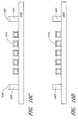
- FIG. 8Aillustrates an embodiment of a packaging structure 800 that comprises a substrate 816 with an array 812 of modulators 810 formed thereon, a backplate 828 , and a desiccant 844 .
- the illustrated package structure 800further comprises a first spacer 825 and a second spacer 826 nested therein.
- a desiccant 848is disposed in the region 846 between the first and second spacers 825 and 826 .
- Other embodimentsdo not comprise a desiccant between the first and second spacers 825 and 826 .
- the second spacer 826acts as a back-up in the event of failure to the first spacer 825 , for example, under extreme environmental conditions and/or in mission critical applications.
- the second spacer 826is relatively permeable to water vapor, thereby permitting any water vapor in and around the array 812 to pass through the second spacer 826 and for absorption by the desiccant 848 .
- the second spacer 826permits the use of a desiccant 848 that may otherwise be unacceptable, for example, a desiccant in the form of a fine powder, a desiccant that generates a powder, a desiccant that generates a vapor, and the like.
- the illustrated configurationalso permits the use of a greater amount of desiccant, thereby increasing the reliability of the device.
- Other embodimentscomprise additional spacers.
- the spacer 825 ′is formed on a recessed cap 828 ′.
- a seal 840 ′extends between a substrate 816 ′ and a backplate 828 ′, and surrounds the spacer 825 ′.
- a portion 840 ′ a of the sealis disposed between the spacer 825 ′ and the substrate 816 ′.
- the portion 840 ′ a of the sealis disposed between the spacer 825 ′ and the backplate 828 ′.
- the height of portion 840 ′ ais less than about 20 ⁇ m, for example from about 5 ⁇ m to about 10 ⁇ m.
- the portion of the seal 840 ′ b that extends between the substrate 816 ′ and the backplate 828 ′serves as a primary barrier layer and the spacer 825 ′ acts as a secondary barrier layer.
- the seal materialis selected to provide a hermetic or semi-hermetic seal.
- the spacer 825 ′is the primary moisture barrier. Suitable materials for the seal 840 ′ are described above.
- the seal 840 ′is an adhesive, for example, an epoxy, silicone, urethane, and the like.
- the spacer 825 ′acts as a dam, reducing the flow of adhesive into the interior of the package structure 800 ′ during its fabrication.
- the dam effect of the spacer 825 ′permits positioning the seal 840 ′ closer to the center of the package structure 800 ′, thereby permitting the manufacture of a smaller device.
- a spacer 825 ′is formed on the backplate 828 ′.
- a bead of adhesiveis applied to the contact area of the substrate 816 ′.
- the adhesiveforms the seal 840 ′.
- the backplate 828 ′ and substrate 816 ′are then positioned, one above the other.
- the spacer 825 ′contacts the bead of adhesive. As the components are brought closer together, the adhesive tends to flow towards the outside of the spacer 825 ′ because the air trapped within the device prevents substantial adhesive flow towards the inside.
- the layer of adhesive remaining between the substrate 816 ′ and the spacer 825 ′forms portion 840 ′ a of the seal.
- the adhesive that flows around the outside of the spacer 825 ′forms portion 840 ′ b of the seal.
- FIG. 9is a flowchart of an embodiment of a method for fabricating a packaging structure with reference to the structures illustrated in cross section in FIG. 10A-FIG . 10 F, which schematically illustrate an embodiment of the process of FIG. 9 .
- a layer of patternable material 1036is deposited. Suitable materials are discussed above.
- the patternable material 1036is deposited over a substrate 1016 and interferometric modulators 1010 supported thereon.
- the modulators 1010 on a surface of the substrate 1016 illustrated in FIG. 10Aare fabricated in an earlier process, for example, a process described U.S. Published Application 2004/0051929.
- Those skilled in the artwill understand that other processes are useful for fabricating either the same type of modulator 1010 or other types modulators, all of which are contemplated as within the present disclosure.
- the systems, apparatus, and methods disclosed hereinare also applicable to other types of MEMS structures.
- the patternable material 1036is deposited on the backplate 1028 .
- the layer of patternable material 1036is deposited using any suitable method known in the art, for example, spin coating, sputtering, physical vapor deposition, chemical vapor deposition, and the like. Those skilled in the art will understand that the particular method or methods used to deposit the layer depends on the particular patternable material or materials used. In the embodiment illustrated in FIG. 10A , the layer of patternable material 1036 covers the modulators 1010 . In other embodiments, the layer of patternable material 1036 does not cover the modulators 1010 . In the illustrated embodiment, the thickness of the layer of patternable material 1036 depends on the desired separation between the substrate 1016 and/or the tops of the modulators 1010 , and the backplate 1028 (illustrated in FIG. 10E ).
- the desired separation between the substrate 1016 and the backplate 1028is from about 100 ⁇ m to about 5 mm. Consequently, the layer of patternable material 1036 has the same or a similar thickness. In other embodiments, the desired separation between the substrate 1016 and/or the tops of the modulators 1010 , and the backplate 1028 has a different value, and the thickness of the layer of patternable material 1036 is adjusted accordingly. As discussed above, a recessed backplate, for example as illustrated in FIG. 7B , provides an equivalent headspace using a shorter spacer 1025 .
- a mask 1038is formed on the layer of patternable material 1036 , as illustrated in FIG. 10B .
- the particular material and method used for forming the mask 1038depends on factors known to those skilled in the art, including, for example, the particular patternable material, the curing conditions for the mask material, the etching conditions for the mask material, the etching conditions for the patternable material, the materials used in the fabrication of the modulators 1010 , the substrate, subsequent process steps and materials, and the like.
- the mask 1038comprises a photoresist.
- the photoresistis a positive resist. In other embodiments, the photoresist is a negative resist.
- the mask 1038is formed using a process comprising exposing the photoresist using a suitable radiation source and pattern, and developed the exposed material to provide a mask 1038 with the desired pattern.
- a suitable radiation source and patterne.g., a UV light, a UV light, or a UV light.
- the mask 1038is printed, for example, by inkjet printing, screen printing, or contact printing.
- the mask 1038is used to pattern the layer of patternable material 1036 to form the spacer 1025 . Consequently, the mask 1038 has a shape and dimensions substantially matching the shape and dimensions of the desired spacer 1025 .
- the spacer 1025is configured to extend about a perimeter surrounding the array 1012 of modulators 1010 .
- the patternable materialis etched to form the spacer 1025 , as illustrated in FIG. 10C .
- the mask 1038is formed, the unmasked portions of the patternable material 1036 are etched.
- the etching methodis selected according to the selected mask material, the selected patternable material, and the other materials used in the device. Suitable etching methods include dry etching and wet etching. In the etching process, patternable material beneath the mask 1038 is shielded from etchant, thereby forming the spacer 1025 .
- step 940the mask 1038 is removed to provide the structure illustrated in FIG. 10D using methods known in the art.
- the structure illustrated in FIG. 10Dis fabricated without forming a mask 1038 or an etching step.
- the patternable material 1036 deposited in step 910comprises a photopatternable material, for example, a photoresist.
- the photopatternable material 1036is then exposed and developed as described above to form the spacer 1025 directly.
- the spacer 1025undergoes additional processing.
- an additional layer of a patternable materialis deposited and patterned as described above, for example, to fabricate a composite and/or higher spacer 1025 .
- the spacer 1025is planarized, for example, by mechanical or chemical-mechanical planarization.
- an adhesive 1040is applied to the top 1034 of the spacer, as illustrated in FIG. 10E .
- Suitable adhesivesare discussed above.
- the adhesive 1040is applied using any method known in the art, for example, by screen printing, inkjet printing, contact printing, or as an adhesive film.
- the adhesive 1040is applied to the backplate 1028 by any suitable method, for example, by screen printing, inkjet printing, contact printing, or as an adhesive film.
- Those skilled in the artwill appreciate that other methods are useful for applying the adhesive 1040 . As discussed above, some embodiments do not use an adhesive. Accordingly, step 950 is optional.
- step 960the backplate 1028 is secured to the spacer 1025 , as illustrated in FIG. 10F .
- the substrate 1016is sealed to the spacer 1025 .
- the backplate 1028is positioned and contacted with the adhesive 1040 . Suitable adhesives are described above.
- the adhesive 1040is then cured under conditions suitable for the adhesive, for example, by UV or thermal curing.
- the backplate 1028 or substrate 1016are sealed to the spacer 1025 using another method, for example, by thermal welding.
- the backplate 1028 and substrate 1016form a cavity 1042 in the package structure 1000 in which the array 1012 is disposed.
- the spacer 1025establishes the distance between the backplate 1028 and the substrate 1016 , and consequently, the height of the cavity 1042 .
- the height of this cavity 1042is selected to permit the unimpaired operation of the modulators 1010 .
- the backplate 1028further comprises a desiccant 1044 secured thereto. Suitable desiccants are discussed above.
- the desiccantis secured to the backplate 1028 , for example, using an adhesive and/or mechanically, prior to securing the backplate 1028 to the spacer 1025 . Accordingly, the desiccant 1044 is sealed within the cavity 1042 of the package structure.
- the desiccant 1044is in the form of a sheet adhered to the backplate 1028 between the modulators 1010 and the backplate 1028 .
- the desiccant 1044has another shape and/or is disposed in a different location in the cavity 1042 .
- a desiccant 1044is disposed in another location, for example, between the spacer 1025 and array 1012 .
- the desiccant 1044is provided a plurality of packages within the cavity 1042 , for example, in bags or capsules.
- height of spacer 1025is adjusted to take into account the dimensions of the desiccant in order to provide sufficient clearance for the operation of the modulators 1010 .
- the spacer 1025is formed on the backplate 1028 rather than on the substrate 1016 . Accordingly, in step 910 , a layer of patternable material 1036 is deposited on a backplate 1028 . In step 920 , a mask 1038 is formed on the layer of patternable material 1036 . In step 930 , the patternable material is etched to form the spacer 1025 . In step 940 , the mask is removed. In step 950 , an adhesive 1040 is applied to the spacer 1025 . In step 960 , a substrate 1016 on which an array of modulators 1010 is supported is secured to the spacer 1025 . As discussed above, in some embodiments, the spacer 1025 comprises a photopatternable material, for example, a photoresist, and consequently, separate masking and etching steps are not required.
- a photopatternable materialfor example, a photoresist
- the spaceris silicon dioxide.
- An interferometric arraywas fabricated as described in U.S. Published Application 2004/0051929 through the step just prior to the sacrificial or release etch. A layer of silicon dioxide was deposited over the partially fabricated array. In different experiments, the silicon dioxide layer was from 5000 ⁇ to 5 ⁇ m thick. Thicker layers were used in some experiments.
- the spacerwas formed from the silicon dioxide layer by conventional masking using a photoresist, and etching. A release etch was then performed as described in U.S. Published Application 2004/0051929. An epoxy adhesive was applied to the contact area on the backplate and the backplate adhered to the spacer. Both planar and recessed backplates were used.
- the spacerswere SU-8 photoresist (Microchem Corp), 5000 ⁇ to 10 ⁇ m thick.
- the photoresistwas spin-coated onto the substrate prior to the sacrificial etch step, then exposed and developed. The sacrificial release etch was then performed.
- An epoxy adhesivewas applied to the backplate, and the package assembled. Both planar and recessed backplates were used.
Landscapes
- Physics & Mathematics (AREA)
- Engineering & Computer Science (AREA)
- Microelectronics & Electronic Packaging (AREA)
- Manufacturing & Machinery (AREA)
- General Physics & Mathematics (AREA)
- Optics & Photonics (AREA)
- Spectroscopy & Molecular Physics (AREA)
- Mechanical Light Control Or Optical Switches (AREA)
- Micromachines (AREA)
Abstract
Description
Claims (23)
Priority Applications (11)
| Application Number | Priority Date | Filing Date | Title |
|---|---|---|---|
| US11/074,253US7701631B2 (en) | 2004-09-27 | 2005-03-07 | Device having patterned spacers for backplates and method of making the same |
| AU2005203725AAU2005203725A1 (en) | 2004-09-27 | 2005-08-19 | Device having patterned spacers for backplates and method of making the same |
| JP2005253640AJP2006099096A (en) | 2004-09-27 | 2005-09-01 | Device having patterned spacer for backplate and method of making the same |
| MXPA05009402AMXPA05009402A (en) | 2004-09-27 | 2005-09-02 | Device having patterned spacers for backplates and method of making the same. |
| TW094130566ATW200626484A (en) | 2004-09-27 | 2005-09-06 | Device having patterned spacers for backplates and method of making the same |
| CA002518808ACA2518808A1 (en) | 2004-09-27 | 2005-09-12 | Device having patterned spacers for backplates and method of making the same |
| SG200505839ASG121121A1 (en) | 2004-09-27 | 2005-09-12 | Device having patterned spacers for backplates andmethod of making the same |
| EP05255700AEP1640775A1 (en) | 2004-09-27 | 2005-09-14 | Interferometric modulator display having patterned spacers for backplates and method of making the same |
| BRPI0503866-9ABRPI0503866A (en) | 2004-09-27 | 2005-09-26 | device having standard backing plate spacers and method of doing the same |
| RU2005129923/28ARU2005129923A (en) | 2004-09-27 | 2005-09-26 | DEVICE WITH STRUCTURED SPACING ELEMENTS FOR REAR WALLS AND METHOD FOR ITS MANUFACTURE |
| KR1020050089842AKR20060092919A (en) | 2004-09-27 | 2005-09-27 | Apparatus having a spacer for a patterned back plate and a method of manufacturing the same |
Applications Claiming Priority (2)
| Application Number | Priority Date | Filing Date | Title |
|---|---|---|---|
| US61347804P | 2004-09-27 | 2004-09-27 | |
| US11/074,253US7701631B2 (en) | 2004-09-27 | 2005-03-07 | Device having patterned spacers for backplates and method of making the same |
Publications (2)
| Publication Number | Publication Date |
|---|---|
| US20060077145A1 US20060077145A1 (en) | 2006-04-13 |
| US7701631B2true US7701631B2 (en) | 2010-04-20 |
Family
ID=35457583
Family Applications (1)
| Application Number | Title | Priority Date | Filing Date |
|---|---|---|---|
| US11/074,253Expired - Fee RelatedUS7701631B2 (en) | 2004-09-27 | 2005-03-07 | Device having patterned spacers for backplates and method of making the same |
Country Status (11)
| Country | Link |
|---|---|
| US (1) | US7701631B2 (en) |
| EP (1) | EP1640775A1 (en) |
| JP (1) | JP2006099096A (en) |
| KR (1) | KR20060092919A (en) |
| AU (1) | AU2005203725A1 (en) |
| BR (1) | BRPI0503866A (en) |
| CA (1) | CA2518808A1 (en) |
| MX (1) | MXPA05009402A (en) |
| RU (1) | RU2005129923A (en) |
| SG (1) | SG121121A1 (en) |
| TW (1) | TW200626484A (en) |
Cited By (9)
| Publication number | Priority date | Publication date | Assignee | Title |
|---|---|---|---|---|
| US20110012219A1 (en)* | 2007-09-28 | 2011-01-20 | Qualcomm Mems Technologies, Inc. | Optimization of desiccant usage in a mems package |
| US20110193184A1 (en)* | 2010-02-10 | 2011-08-11 | Christian Solf | Micromechanical system and method for manufacturing a micromechanical system |
| WO2011130715A2 (en) | 2010-04-16 | 2011-10-20 | Flex Lighting Ii, Llc | Illumination device comprising a film-based lightguide |
| WO2011130718A2 (en) | 2010-04-16 | 2011-10-20 | Flex Lighting Ii, Llc | Front illumination device comprising a film-based lightguide |
| US20120099179A1 (en)* | 2004-09-27 | 2012-04-26 | Qualcomm Mems Technologies, Inc. | Method and device for providing electronic circuitry on a backplate |
| US20120327092A1 (en)* | 2011-06-21 | 2012-12-27 | Qualcomm Mems Technologies, Inc. | Planarized spacer for cover plate over electromechanical systems device array |
| US20140041208A1 (en)* | 2009-04-21 | 2014-02-13 | Fujitsu Component Limited | Touchscreen panel, electronic apparatus and method of fabricating touchscreen panel |
| US20160358832A1 (en)* | 2015-06-02 | 2016-12-08 | Ngk Spark Plug Co., Ltd. | Ceramic package and manufacturing method therefor |
| US9950922B2 (en) | 2014-03-17 | 2018-04-24 | The Regents Of The University Of Michigan | Packaged microsystems |
Families Citing this family (23)
| Publication number | Priority date | Publication date | Assignee | Title |
|---|---|---|---|---|
| US7626581B2 (en)* | 2004-09-27 | 2009-12-01 | Idc, Llc | Device and method for display memory using manipulation of mechanical response |
| JP2006224193A (en)* | 2005-02-15 | 2006-08-31 | Olympus Corp | Electronic device and manufacturing method of electronic device |
| US7561334B2 (en)* | 2005-12-20 | 2009-07-14 | Qualcomm Mems Technologies, Inc. | Method and apparatus for reducing back-glass deflection in an interferometric modulator display device |
| US8194056B2 (en)* | 2006-02-09 | 2012-06-05 | Qualcomm Mems Technologies Inc. | Method and system for writing data to MEMS display elements |
| WO2007120887A2 (en)* | 2006-04-13 | 2007-10-25 | Qualcomm Mems Technologies, Inc | Packaging a mems device using a frame |
| WO2007136706A1 (en)* | 2006-05-17 | 2007-11-29 | Qualcomm Mems Technologies Inc. | Desiccant in a mems device |
| EP2029473A2 (en)* | 2006-06-21 | 2009-03-04 | Qualcomm Incorporated | Method for packaging an optical mems device |
| US7816164B2 (en)* | 2006-12-01 | 2010-10-19 | Qualcomm Mems Technologies, Inc. | MEMS processing |
| US7719752B2 (en)* | 2007-05-11 | 2010-05-18 | Qualcomm Mems Technologies, Inc. | MEMS structures, methods of fabricating MEMS components on separate substrates and assembly of same |
| GB2453104B (en)* | 2007-09-19 | 2012-04-25 | Wolfson Microelectronics Plc | Mems device and process |
| GB2452941B (en)* | 2007-09-19 | 2012-04-11 | Wolfson Microelectronics Plc | Mems device and process |
| US20090323170A1 (en)* | 2008-06-30 | 2009-12-31 | Qualcomm Mems Technologies, Inc. | Groove on cover plate or substrate |
| US20100020382A1 (en)* | 2008-07-22 | 2010-01-28 | Qualcomm Mems Technologies, Inc. | Spacer for mems device |
| US8410690B2 (en)* | 2009-02-13 | 2013-04-02 | Qualcomm Mems Technologies, Inc. | Display device with desiccant |
| US8379392B2 (en)* | 2009-10-23 | 2013-02-19 | Qualcomm Mems Technologies, Inc. | Light-based sealing and device packaging |
| SE534411C2 (en)* | 2009-11-02 | 2011-08-09 | Stanley Wissmar | Electronic Finger Ring and manufacture of the same |
| JP5310529B2 (en)* | 2009-12-22 | 2013-10-09 | 株式会社豊田中央研究所 | Oscillator for plate member |
| US20120242638A1 (en)* | 2011-03-24 | 2012-09-27 | Qualcomm Mems Technologies, Inc. | Dielectric spacer for display devices |
| JP2017181624A (en)* | 2016-03-29 | 2017-10-05 | セイコーエプソン株式会社 | Electro-optical device, electro-optical unit, and electronic apparatus |
| WO2018012108A1 (en)* | 2016-07-12 | 2018-01-18 | ソニー株式会社 | Dimming device, image display device, and display device |
| US20220219125A1 (en)* | 2019-05-01 | 2022-07-14 | King Abdullah University Of Science And Technology | Hybrid inorganic oxide-carbon molecular sieve membranes |
| US11244876B2 (en) | 2019-10-09 | 2022-02-08 | Microchip Technology Inc. | Packaged semiconductor die with micro-cavity |
| KR20210126175A (en)* | 2020-04-09 | 2021-10-20 | 삼성디스플레이 주식회사 | Display device |
Citations (330)
| Publication number | Priority date | Publication date | Assignee | Title |
|---|---|---|---|---|
| US2534846A (en) | 1946-06-20 | 1950-12-19 | Emi Ltd | Color filter |
| US3439973A (en) | 1963-06-28 | 1969-04-22 | Siemens Ag | Polarizing reflector for electromagnetic wave radiation in the micron wavelength |
| US3653741A (en) | 1970-02-16 | 1972-04-04 | Alvin M Marks | Electro-optical dipolar material |
| US3656836A (en) | 1968-07-05 | 1972-04-18 | Thomson Csf | Light modulator |
| US3813265A (en) | 1970-02-16 | 1974-05-28 | A Marks | Electro-optical dipolar material |
| US3955880A (en) | 1973-07-20 | 1976-05-11 | Organisation Europeenne De Recherches Spatiales | Infrared radiation modulator |
| US4036360A (en) | 1975-11-12 | 1977-07-19 | Graham Magnetics Incorporated | Package having dessicant composition |
| US4074480A (en) | 1976-02-12 | 1978-02-21 | Burton Henry W G | Kit for converting single-glazed window to double-glazed window |
| US4099854A (en) | 1976-10-12 | 1978-07-11 | The Unites States Of America As Represented By The Secretary Of The Navy | Optical notch filter utilizing electric dipole resonance absorption |
| US4228437A (en) | 1979-06-26 | 1980-10-14 | The United States Of America As Represented By The Secretary Of The Navy | Wideband polarization-transforming electromagnetic mirror |
| US4310220A (en) | 1977-01-24 | 1982-01-12 | Sharp Kabushiki Kaisha | Electrochromic display with one porous separator |
| US4377324A (en) | 1980-08-04 | 1983-03-22 | Honeywell Inc. | Graded index Fabry-Perot optical filter device |
| US4383255A (en) | 1980-03-11 | 1983-05-10 | Centre Electronique Horloger S.A. | Miniature display device |
| US4389096A (en) | 1977-12-27 | 1983-06-21 | Matsushita Electric Industrial Co., Ltd. | Image display apparatus of liquid crystal valve projection type |
| US4403248A (en) | 1980-03-04 | 1983-09-06 | U.S. Philips Corporation | Display device with deformable reflective medium |
| US4431691A (en) | 1979-01-29 | 1984-02-14 | Tremco, Incorporated | Dimensionally stable sealant and spacer strip and composite structures comprising the same |
| US4441791A (en) | 1980-09-02 | 1984-04-10 | Texas Instruments Incorporated | Deformable mirror light modulator |
| US4445050A (en) | 1981-12-15 | 1984-04-24 | Marks Alvin M | Device for conversion of light power to electric power |
| US4482213A (en) | 1982-11-23 | 1984-11-13 | Texas Instruments Incorporated | Perimeter seal reinforcement holes for plastic LCDs |
| US4500171A (en) | 1982-06-02 | 1985-02-19 | Texas Instruments Incorporated | Process for plastic LCD fill hole sealing |
| US4519676A (en) | 1982-02-01 | 1985-05-28 | U.S. Philips Corporation | Passive display device |
| US4531126A (en) | 1981-05-18 | 1985-07-23 | Societe D'etude Du Radant | Method and device for analyzing a very high frequency radiation beam of electromagnetic waves |
| US4566935A (en) | 1984-07-31 | 1986-01-28 | Texas Instruments Incorporated | Spatial light modulator and method |
| US4571603A (en) | 1981-11-03 | 1986-02-18 | Texas Instruments Incorporated | Deformable mirror electrostatic printer |
| US4596992A (en) | 1984-08-31 | 1986-06-24 | Texas Instruments Incorporated | Linear spatial light modulator and printer |
| US4615595A (en) | 1984-10-10 | 1986-10-07 | Texas Instruments Incorporated | Frame addressed spatial light modulator |
| US4663083A (en) | 1978-05-26 | 1987-05-05 | Marks Alvin M | Electro-optical dipole suspension with reflective-absorptive-transmissive characteristics |
| US4662746A (en) | 1985-10-30 | 1987-05-05 | Texas Instruments Incorporated | Spatial light modulator and method |
| US4681403A (en) | 1981-07-16 | 1987-07-21 | U.S. Philips Corporation | Display device with micromechanical leaf spring switches |
| US4710732A (en) | 1984-07-31 | 1987-12-01 | Texas Instruments Incorporated | Spatial light modulator and method |
| US4748366A (en) | 1986-09-02 | 1988-05-31 | Taylor George W | Novel uses of piezoelectric materials for creating optical effects |
| US4786128A (en) | 1986-12-02 | 1988-11-22 | Quantum Diagnostics, Ltd. | Device for modulating and reflecting electromagnetic radiation employing electro-optic layer having a variable index of refraction |
| US4790635A (en) | 1986-04-25 | 1988-12-13 | The Secretary Of State For Defence In Her Brittanic Majesty's Government Of The United Kingdom Of Great Britain And Northern Ireland | Electro-optical device |
| US4856863A (en) | 1988-06-22 | 1989-08-15 | Texas Instruments Incorporated | Optical fiber interconnection network including spatial light modulator |
| US4954789A (en) | 1989-09-28 | 1990-09-04 | Texas Instruments Incorporated | Spatial light modulator |
| US4956619A (en) | 1988-02-19 | 1990-09-11 | Texas Instruments Incorporated | Spatial light modulator |
| US4977009A (en) | 1987-12-16 | 1990-12-11 | Ford Motor Company | Composite polymer/desiccant coatings for IC encapsulation |
| US4982184A (en) | 1989-01-03 | 1991-01-01 | General Electric Company | Electrocrystallochromic display and element |
| US5018256A (en) | 1990-06-29 | 1991-05-28 | Texas Instruments Incorporated | Architecture and process for integrating DMD with control circuit substrates |
| US5022745A (en) | 1989-09-07 | 1991-06-11 | Massachusetts Institute Of Technology | Electrostatically deformable single crystal dielectrically coated mirror |
| US5028939A (en) | 1988-08-23 | 1991-07-02 | Texas Instruments Incorporated | Spatial light modulator system |
| US5037173A (en) | 1989-11-22 | 1991-08-06 | Texas Instruments Incorporated | Optical interconnection network |
| US5044736A (en) | 1990-11-06 | 1991-09-03 | Motorola, Inc. | Configurable optical filter or display |
| US5061049A (en) | 1984-08-31 | 1991-10-29 | Texas Instruments Incorporated | Spatial light modulator and method |
| US5075796A (en) | 1990-05-31 | 1991-12-24 | Eastman Kodak Company | Optical article for multicolor imaging |
| US5078479A (en) | 1990-04-20 | 1992-01-07 | Centre Suisse D'electronique Et De Microtechnique Sa | Light modulation device with matrix addressing |
| US5079544A (en) | 1989-02-27 | 1992-01-07 | Texas Instruments Incorporated | Standard independent digitized video system |
| US5083857A (en) | 1990-06-29 | 1992-01-28 | Texas Instruments Incorporated | Multi-level deformable mirror device |
| US5096279A (en) | 1984-08-31 | 1992-03-17 | Texas Instruments Incorporated | Spatial light modulator and method |
| US5099353A (en) | 1990-06-29 | 1992-03-24 | Texas Instruments Incorporated | Architecture and process for integrating DMD with control circuit substrates |
| US5124834A (en) | 1989-11-16 | 1992-06-23 | General Electric Company | Transferrable, self-supporting pellicle for elastomer light valve displays and method for making the same |
| US5142405A (en) | 1990-06-29 | 1992-08-25 | Texas Instruments Incorporated | Bistable dmd addressing circuit and method |
| US5142414A (en) | 1991-04-22 | 1992-08-25 | Koehler Dale R | Electrically actuatable temporal tristimulus-color device |
| US5153771A (en) | 1990-07-18 | 1992-10-06 | Northrop Corporation | Coherent light modulation and detector |
| US5162787A (en) | 1989-02-27 | 1992-11-10 | Texas Instruments Incorporated | Apparatus and method for digitized video system utilizing a moving display surface |
| US5168406A (en) | 1991-07-31 | 1992-12-01 | Texas Instruments Incorporated | Color deformable mirror device and method for manufacture |
| US5170156A (en) | 1989-02-27 | 1992-12-08 | Texas Instruments Incorporated | Multi-frequency two dimensional display system |
| US5172262A (en) | 1985-10-30 | 1992-12-15 | Texas Instruments Incorporated | Spatial light modulator and method |
| US5179274A (en) | 1991-07-12 | 1993-01-12 | Texas Instruments Incorporated | Method for controlling operation of optical systems and devices |
| US5192395A (en) | 1990-10-12 | 1993-03-09 | Texas Instruments Incorporated | Method of making a digital flexure beam accelerometer |
| US5192946A (en) | 1989-02-27 | 1993-03-09 | Texas Instruments Incorporated | Digitized color video display system |
| US5206629A (en) | 1989-02-27 | 1993-04-27 | Texas Instruments Incorporated | Spatial light modulator and memory for digitized video display |
| US5214419A (en) | 1989-02-27 | 1993-05-25 | Texas Instruments Incorporated | Planarized true three dimensional display |
| US5214420A (en) | 1989-02-27 | 1993-05-25 | Texas Instruments Incorporated | Spatial light modulator projection system with random polarity light |
| US5216537A (en) | 1990-06-29 | 1993-06-01 | Texas Instruments Incorporated | Architecture and process for integrating DMD with control circuit substrates |
| US5226099A (en) | 1991-04-26 | 1993-07-06 | Texas Instruments Incorporated | Digital micromirror shutter device |
| US5231532A (en) | 1992-02-05 | 1993-07-27 | Texas Instruments Incorporated | Switchable resonant filter for optical radiation |
| US5233456A (en) | 1991-12-20 | 1993-08-03 | Texas Instruments Incorporated | Resonant mirror and method of manufacture |
| US5233385A (en) | 1991-12-18 | 1993-08-03 | Texas Instruments Incorporated | White light enhanced color field sequential projection |
| US5233459A (en) | 1991-03-06 | 1993-08-03 | Massachusetts Institute Of Technology | Electric display device |
| US5244707A (en) | 1992-01-10 | 1993-09-14 | Shores A Andrew | Enclosure for electronic devices |
| US5254980A (en) | 1991-09-06 | 1993-10-19 | Texas Instruments Incorporated | DMD display system controller |
| US5268533A (en) | 1991-05-03 | 1993-12-07 | Hughes Aircraft Company | Pre-stressed laminated lid for electronic circuit package |
| US5272473A (en) | 1989-02-27 | 1993-12-21 | Texas Instruments Incorporated | Reduced-speckle display system |
| US5278652A (en) | 1991-04-01 | 1994-01-11 | Texas Instruments Incorporated | DMD architecture and timing for use in a pulse width modulated display system |
| US5280277A (en) | 1990-06-29 | 1994-01-18 | Texas Instruments Incorporated | Field updated deformable mirror device |
| US5287096A (en) | 1989-02-27 | 1994-02-15 | Texas Instruments Incorporated | Variable luminosity display system |
| US5296950A (en) | 1992-01-31 | 1994-03-22 | Texas Instruments Incorporated | Optical signal free-space conversion board |
| US5304419A (en) | 1990-07-06 | 1994-04-19 | Alpha Fry Ltd | Moisture and particle getter for enclosures |
| US5311360A (en) | 1992-04-28 | 1994-05-10 | The Board Of Trustees Of The Leland Stanford, Junior University | Method and apparatus for modulating a light beam |
| US5312513A (en) | 1992-04-03 | 1994-05-17 | Texas Instruments Incorporated | Methods of forming multiple phase light modulators |
| US5323002A (en) | 1992-03-25 | 1994-06-21 | Texas Instruments Incorporated | Spatial light modulator based optical calibration system |
| US5325116A (en) | 1992-09-18 | 1994-06-28 | Texas Instruments Incorporated | Device for writing to and reading from optical storage media |
| US5327286A (en) | 1992-08-31 | 1994-07-05 | Texas Instruments Incorporated | Real time optical correlation system |
| US5331454A (en) | 1990-11-13 | 1994-07-19 | Texas Instruments Incorporated | Low reset voltage process for DMD |
| US5365283A (en) | 1993-07-19 | 1994-11-15 | Texas Instruments Incorporated | Color phase control for projection display using spatial light modulator |
| US5381253A (en) | 1991-11-14 | 1995-01-10 | Board Of Regents Of University Of Colorado | Chiral smectic liquid crystal optical modulators having variable retardation |
| US5401983A (en) | 1992-04-08 | 1995-03-28 | Georgia Tech Research Corporation | Processes for lift-off of thin film materials or devices for fabricating three dimensional integrated circuits, optical detectors, and micromechanical devices |
| EP0667548A1 (en) | 1994-01-27 | 1995-08-16 | AT&T Corp. | Micromechanical modulator |
| US5444566A (en) | 1994-03-07 | 1995-08-22 | Texas Instruments Incorporated | Optimized electronic operation of digital micromirror devices |
| US5446479A (en) | 1989-02-27 | 1995-08-29 | Texas Instruments Incorporated | Multi-dimensional array video processor system |
| US5448314A (en) | 1994-01-07 | 1995-09-05 | Texas Instruments | Method and apparatus for sequential color imaging |
| US5452024A (en) | 1993-11-01 | 1995-09-19 | Texas Instruments Incorporated | DMD display system |
| US5454906A (en) | 1994-06-21 | 1995-10-03 | Texas Instruments Inc. | Method of providing sacrificial spacer for micro-mechanical devices |
| US5457566A (en) | 1991-11-22 | 1995-10-10 | Texas Instruments Incorporated | DMD scanner |
| US5457493A (en) | 1993-09-15 | 1995-10-10 | Texas Instruments Incorporated | Digital micro-mirror based image simulation system |
| US5459602A (en) | 1993-10-29 | 1995-10-17 | Texas Instruments | Micro-mechanical optical shutter |
| US5461411A (en) | 1993-03-29 | 1995-10-24 | Texas Instruments Incorporated | Process and architecture for digital micromirror printer |
| US5489952A (en) | 1993-07-14 | 1996-02-06 | Texas Instruments Incorporated | Method and device for multi-format television |
| EP0695959A1 (en) | 1994-07-29 | 1996-02-07 | AT&T Corp. | Direct view display based on a micromechanical modulator |
| US5497197A (en) | 1993-11-04 | 1996-03-05 | Texas Instruments Incorporated | System and method for packaging data into video processor |
| US5497172A (en) | 1994-06-13 | 1996-03-05 | Texas Instruments Incorporated | Pulse width modulation for spatial light modulator with split reset addressing |
| US5499062A (en) | 1994-06-23 | 1996-03-12 | Texas Instruments Incorporated | Multiplexed memory timing with block reset and secondary memory |
| US5500635A (en) | 1990-02-20 | 1996-03-19 | Mott; Jonathan C. | Products incorporating piezoelectric material |
| US5506597A (en) | 1989-02-27 | 1996-04-09 | Texas Instruments Incorporated | Apparatus and method for image projection |
| US5517347A (en) | 1993-12-01 | 1996-05-14 | Texas Instruments Incorporated | Direct view deformable mirror device |
| US5526051A (en) | 1993-10-27 | 1996-06-11 | Texas Instruments Incorporated | Digital television system |
| US5526172A (en) | 1993-07-27 | 1996-06-11 | Texas Instruments Incorporated | Microminiature, monolithic, variable electrical signal processor and apparatus including same |
| US5526688A (en) | 1990-10-12 | 1996-06-18 | Texas Instruments Incorporated | Digital flexure beam accelerometer and method |
| US5535047A (en) | 1995-04-18 | 1996-07-09 | Texas Instruments Incorporated | Active yoke hidden hinge digital micromirror device |
| US5548301A (en) | 1993-01-11 | 1996-08-20 | Texas Instruments Incorporated | Pixel control circuitry for spatial light modulator |
| US5552924A (en) | 1994-11-14 | 1996-09-03 | Texas Instruments Incorporated | Micromechanical device having an improved beam |
| US5563398A (en) | 1991-10-31 | 1996-10-08 | Texas Instruments Incorporated | Spatial light modulator scanning system |
| US5567334A (en) | 1995-02-27 | 1996-10-22 | Texas Instruments Incorporated | Method for creating a digital micromirror device using an aluminum hard mask |
| US5579149A (en) | 1993-09-13 | 1996-11-26 | Csem Centre Suisse D'electronique Et De Microtechnique Sa | Miniature network of light obturators |
| US5581272A (en) | 1993-08-25 | 1996-12-03 | Texas Instruments Incorporated | Signal generator for controlling a spatial light modulator |
| US5583688A (en) | 1993-12-21 | 1996-12-10 | Texas Instruments Incorporated | Multi-level digital micromirror device |
| US5597736A (en) | 1992-08-11 | 1997-01-28 | Texas Instruments Incorporated | High-yield spatial light modulator with light blocking layer |
| US5602671A (en) | 1990-11-13 | 1997-02-11 | Texas Instruments Incorporated | Low surface energy passivation layer for micromechanical devices |
| US5610624A (en) | 1994-11-30 | 1997-03-11 | Texas Instruments Incorporated | Spatial light modulator with reduced possibility of an on state defect |
| US5610625A (en) | 1992-05-20 | 1997-03-11 | Texas Instruments Incorporated | Monolithic spatial light modulator and memory package |
| US5610438A (en) | 1995-03-08 | 1997-03-11 | Texas Instruments Incorporated | Micro-mechanical device with non-evaporable getter |
| US5619059A (en) | 1994-09-28 | 1997-04-08 | National Research Council Of Canada | Color deformable mirror device having optical thin film interference color coatings |
| US5619366A (en) | 1992-06-08 | 1997-04-08 | Texas Instruments Incorporated | Controllable surface filter |
| US5646768A (en) | 1994-07-29 | 1997-07-08 | Texas Instruments Incorporated | Support posts for micro-mechanical devices |
| US5650881A (en) | 1994-11-02 | 1997-07-22 | Texas Instruments Incorporated | Support post architecture for micromechanical devices |
| US5654741A (en) | 1994-05-17 | 1997-08-05 | Texas Instruments Incorporation | Spatial light modulator display pointing device |
| US5659374A (en) | 1992-10-23 | 1997-08-19 | Texas Instruments Incorporated | Method of repairing defective pixels |
| US5665997A (en) | 1994-03-31 | 1997-09-09 | Texas Instruments Incorporated | Grated landing area to eliminate sticking of micro-mechanical devices |
| US5703710A (en) | 1994-09-09 | 1997-12-30 | Deacon Research | Method for manipulating optical energy using poled structure |
| US5710656A (en) | 1996-07-30 | 1998-01-20 | Lucent Technologies Inc. | Micromechanical optical modulator having a reduced-mass composite membrane |
| US5717476A (en) | 1995-01-13 | 1998-02-10 | Seiko Epson Corporation | Liquid crystal display device and manfacturing method therefor |
| US5739945A (en) | 1995-09-29 | 1998-04-14 | Tayebati; Parviz | Electrically tunable optical filter utilizing a deformable multi-layer mirror |
| US5745281A (en) | 1995-12-29 | 1998-04-28 | Hewlett-Packard Company | Electrostatically-driven light modulator and display |
| US5771321A (en) | 1996-01-04 | 1998-06-23 | Massachusetts Institute Of Technology | Micromechanical optical switch and flat panel display |
| US5771116A (en) | 1996-10-21 | 1998-06-23 | Texas Instruments Incorporated | Multiple bias level reset waveform for enhanced DMD control |
| US5784190A (en) | 1995-04-27 | 1998-07-21 | John M. Baker | Electro-micro-mechanical shutters on transparent substrates |
| US5815141A (en) | 1996-04-12 | 1998-09-29 | Elo Touch Systems, Inc. | Resistive touchscreen having multiple selectable regions for pressure discrimination |
| EP0822570A3 (en) | 1996-08-02 | 1998-10-14 | Motorola, Inc. | Field emission display and method of making same |
| US5825528A (en) | 1995-12-26 | 1998-10-20 | Lucent Technologies Inc. | Phase-mismatched fabry-perot cavity micromechanical modulator |
| US5835255A (en) | 1986-04-23 | 1998-11-10 | Etalon, Inc. | Visible spectrum modulator arrays |
| US5837562A (en) | 1995-07-07 | 1998-11-17 | The Charles Stark Draper Laboratory, Inc. | Process for bonding a shell to a substrate for packaging a semiconductor |
| US5842088A (en) | 1994-06-17 | 1998-11-24 | Texas Instruments Incorporated | Method of calibrating a spatial light modulator printing system |
| US5853662A (en) | 1996-04-17 | 1998-12-29 | Mitsubishi Gas Chemical Company, Inc. | Method for preserving polished inorganic glass and method for preserving article obtained by using the same |
| US5856820A (en) | 1995-02-24 | 1999-01-05 | The Whitaker Corporation | Laminated acoustic wave touch panel |
| US5912758A (en) | 1996-09-11 | 1999-06-15 | Texas Instruments Incorporated | Bipolar reset for spatial light modulators |
| US5936758A (en) | 1996-04-12 | 1999-08-10 | Texas Instruments Incorporated | Method of passivating a micromechanical device within a hermetic package |
| US5939785A (en) | 1996-04-12 | 1999-08-17 | Texas Instruments Incorporated | Micromechanical device including time-release passivant |
| WO1999052006A2 (en) | 1998-04-08 | 1999-10-14 | Etalon, Inc. | Interferometric modulation of radiation |
| US5999306A (en) | 1995-12-01 | 1999-12-07 | Seiko Epson Corporation | Method of manufacturing spatial light modulator and electronic device employing it |
| US6028690A (en) | 1997-11-26 | 2000-02-22 | Texas Instruments Incorporated | Reduced micromirror mirror gaps for improved contrast ratio |
| US6038056A (en) | 1997-05-08 | 2000-03-14 | Texas Instruments Incorporated | Spatial light modulator having improved contrast ratio |
| US6040937A (en) | 1994-05-05 | 2000-03-21 | Etalon, Inc. | Interferometric modulation |
| US6061075A (en) | 1992-01-23 | 2000-05-09 | Texas Instruments Incorporated | Non-systolic time delay and integration printing |
| US6099132A (en) | 1994-09-23 | 2000-08-08 | Texas Instruments Incorporated | Manufacture method for micromechanical devices |
| US6113239A (en) | 1998-09-04 | 2000-09-05 | Sharp Laboratories Of America, Inc. | Projection display system for reflective light valves |
| US6120339A (en) | 1998-10-26 | 2000-09-19 | Micron Technology, Inc. | Methods of fabricating flat panel evacuated displays |
| US6127765A (en) | 1998-02-24 | 2000-10-03 | Tokyo Institute Of Technology | Micro-electromechanical device |
| US6147790A (en) | 1998-06-02 | 2000-11-14 | Texas Instruments Incorporated | Spring-ring micromechanical device |
| US6160833A (en) | 1998-05-06 | 2000-12-12 | Xerox Corporation | Blue vertical cavity surface emitting laser |
| US6180428B1 (en) | 1997-12-12 | 2001-01-30 | Xerox Corporation | Monolithic scanning light emitting devices using micromachining |
| US6195196B1 (en) | 1998-03-13 | 2001-02-27 | Fuji Photo Film Co., Ltd. | Array-type exposing device and flat type display incorporating light modulator and driving method thereof |
| US6201633B1 (en) | 1999-06-07 | 2001-03-13 | Xerox Corporation | Micro-electromechanical based bistable color display sheets |
| US6232936B1 (en) | 1993-12-03 | 2001-05-15 | Texas Instruments Incorporated | DMD Architecture to improve horizontal resolution |
| US6238755B1 (en) | 1997-11-15 | 2001-05-29 | Dow Corning Corporation | Insulating glass units |
| US20010003487A1 (en) | 1996-11-05 | 2001-06-14 | Mark W. Miles | Visible spectrum modulator arrays |
| US20010004085A1 (en) | 1999-12-15 | 2001-06-21 | Gueissaz Fran?Ccedil;Ois | Method for hermetically encapsulating microsystems in situ |
| US6282010B1 (en) | 1998-05-14 | 2001-08-28 | Texas Instruments Incorporated | Anti-reflective coatings for spatial light modulators |
| US6295154B1 (en) | 1998-06-05 | 2001-09-25 | Texas Instruments Incorporated | Optical switching apparatus |
| US6303986B1 (en) | 1998-07-29 | 2001-10-16 | Silicon Light Machines | Method of and apparatus for sealing an hermetic lid to a semiconductor die |
| JP2001318324A (en) | 2000-05-11 | 2001-11-16 | Seiko Epson Corp | Optical switching unit, method of manufacturing the same, and image display device |
| US6323982B1 (en) | 1998-05-22 | 2001-11-27 | Texas Instruments Incorporated | Yield superstructure for digital micromirror device |
| JP2001351998A (en) | 2000-06-09 | 2001-12-21 | Kyocera Corp | Package for storing semiconductor elements |
| US20020012364A1 (en) | 2000-02-11 | 2002-01-31 | Ron Kalian | Method of synchronising the replay of audio data in a network of computers |
| US20020015215A1 (en) | 1994-05-05 | 2002-02-07 | Iridigm Display Corporation, A Delaware Corporation | Interferometric modulation of radiation |
| JP2002062491A (en) | 2000-08-15 | 2002-02-28 | Canon Inc | Imaging optical system and light amount control device using coherent modulation element |
| JP2002062492A (en) | 2000-08-15 | 2002-02-28 | Canon Inc | Projection optical system using coherent modulator |
| US6365229B1 (en) | 1998-09-30 | 2002-04-02 | Texas Instruments Incorporated | Surface treatment material deposition and recapture |
| US20020043706A1 (en) | 2000-06-28 | 2002-04-18 | Institut National D'optique | Miniature Microdevice Package and Process for Making Thereof |
| US6379988B1 (en) | 2000-05-16 | 2002-04-30 | Sandia Corporation | Pre-release plastic packaging of MEMS and IMEMS devices |
| US20020052392A1 (en) | 2000-10-20 | 2002-05-02 | Day Robert F. | Bita3 adrenergic receptor agonists and uses thereof |
| US20020056898A1 (en) | 2000-11-16 | 2002-05-16 | Lopes Vincent C. | Package with environmental control material carrier |
| US20020057565A1 (en) | 2000-11-14 | 2002-05-16 | Satoshi Seo | Light emitting device |
| US20020056900A1 (en) | 2000-11-16 | 2002-05-16 | Liu Jwei Wien | Electro-optical package with drop-in aperture |
| US20020070931A1 (en) | 2000-07-03 | 2002-06-13 | Hiroichi Ishikawa | Optical multilayer structure, optical switching device, and image display |
| US20020075551A1 (en) | 2000-11-29 | 2002-06-20 | Onix Microsystems, Inc | Enclosure for MEMS apparatus and method of using the same |
| US20020075555A1 (en) | 1994-05-05 | 2002-06-20 | Iridigm Display Corporation | Interferometric modulation of radiation |
| US6426124B2 (en) | 1998-12-21 | 2002-07-30 | Sikorsky Aircraft Corporation | Processed fiber for emission of energy into a medium and method therefor |
| US6426461B1 (en) | 2000-09-21 | 2002-07-30 | Delphi Technologies, Inc. | Enclosure for electronic components |
| JP2002258310A (en) | 2001-02-28 | 2002-09-11 | Kyocera Corp | Liquid crystal display and display equipment |
| US6455927B1 (en) | 2001-03-12 | 2002-09-24 | Amkor Technology, Inc. | Micromirror device package |
| US6462392B1 (en) | 2000-02-04 | 2002-10-08 | Robert Bosch Gmbh | Micromechanical cap structure and the respective manufacturing method |
| JP2002296519A (en) | 2001-03-29 | 2002-10-09 | Ricoh Co Ltd | Optical modulator and method of manufacturing the same, image forming apparatus having the optical modulator, and image projection display device having the optical modulator |
| US6465355B1 (en) | 2001-04-27 | 2002-10-15 | Hewlett-Packard Company | Method of fabricating suspended microstructures |
| US6466354B1 (en) | 2000-09-19 | 2002-10-15 | Silicon Light Machines | Method and apparatus for interferometric modulation of light |
| US6466358B2 (en) | 1999-12-30 | 2002-10-15 | Texas Instruments Incorporated | Analog pulse width modulation cell for digital micromechanical device |
| JP2002312066A (en) | 2001-04-17 | 2002-10-25 | Hunet Inc | Portable computer equipped with removable attached additional display and display module for additional installation of such display |
| US6472739B1 (en) | 1999-11-15 | 2002-10-29 | Jds Uniphase Corporation | Encapsulated microelectromechanical (MEMS) devices |
| US6473274B1 (en) | 2000-06-28 | 2002-10-29 | Texas Instruments Incorporated | Symmetrical microactuator structure for use in mass data storage devices, or the like |
| US20020160583A1 (en) | 2001-04-26 | 2002-10-31 | Samsung Electronics Co., Ltd. | MEMS relay and mehtod of fabricating the same |
| US6480177B2 (en) | 1997-06-04 | 2002-11-12 | Texas Instruments Incorporated | Blocked stepped address voltage for micromechanical devices |
| JP2002328313A (en) | 2001-05-01 | 2002-11-15 | Sony Corp | Optical switching element, method for manufacturing the same, and image display device |
| US6489670B1 (en) | 2000-05-16 | 2002-12-03 | Sandia Corporation | Sealed symmetric multilayered microelectronic device package with integral windows |
| US20020187254A1 (en) | 2001-05-08 | 2002-12-12 | Eastman Kodak Company | Ultrasonically sealing the cover plate to provide a hermetic enclosure for OLED displays |
| JP2002357846A (en) | 2002-04-15 | 2002-12-13 | Sharp Corp | Liquid crystal display device and manufacturing method thereof |
| US6496122B2 (en) | 1998-06-26 | 2002-12-17 | Sharp Laboratories Of America, Inc. | Image display and remote control system capable of displaying two distinct images |
| US6507385B1 (en) | 1999-04-30 | 2003-01-14 | Matsushita Electric Industrial Co., Ltd. | Liquid crystal display element and manufacturing method thereof |
| WO2003007049A1 (en) | 1999-10-05 | 2003-01-23 | Iridigm Display Corporation | Photonic mems and structures |
| US6525416B2 (en) | 2000-10-04 | 2003-02-25 | Infineon Technologies Ag | Electronic devices and a sheet strip for packaging bonding wire connections of electronic devices and method for producing them |
| JP2003075741A (en) | 2001-07-24 | 2003-03-12 | Lucent Technol Inc | Constitution of mems driver circuit |
| US20030054588A1 (en) | 2000-12-07 | 2003-03-20 | Reflectivity, Inc., A California Corporation | Methods for depositing, releasing and packaging micro-electromechanical devices on wafer substrates |
| WO2003026369A1 (en) | 2001-09-17 | 2003-03-27 | John Stafford | Latching micro magnetic relay packages and methods of packaging |
| US20030062186A1 (en) | 2001-09-21 | 2003-04-03 | Eastman Kodak Company | Sealing structure for highly moisture-sensitive electronic device element and method for fabrication |
| US6545335B1 (en) | 1999-12-27 | 2003-04-08 | Xerox Corporation | Structure and method for electrical isolation of optoelectronic integrated circuits |
| US6549338B1 (en) | 1999-11-12 | 2003-04-15 | Texas Instruments Incorporated | Bandpass filter to reduce thermal impact of dichroic light shift |
| US6548908B2 (en) | 1999-12-27 | 2003-04-15 | Xerox Corporation | Structure and method for planar lateral oxidation in passive devices |
| US6552840B2 (en) | 1999-12-03 | 2003-04-22 | Texas Instruments Incorporated | Electrostatic efficiency of micromechanical devices |
| US20030075794A1 (en) | 2001-10-23 | 2003-04-24 | Felton Lawrence E. | MEMS capping method and apparatus |
| US6558820B2 (en) | 2001-05-10 | 2003-05-06 | Eastman Kodak Company | High contrast light-emitting diode devices |
| US6574033B1 (en) | 2002-02-27 | 2003-06-03 | Iridigm Display Corporation | Microelectromechanical systems device and method for fabricating same |
| US20030108306A1 (en) | 2001-12-12 | 2003-06-12 | Axsun Technologies, Inc. | MEMS tunable optical filter system with moisture getter for frequency stability |
| US20030111603A1 (en) | 2001-12-13 | 2003-06-19 | Mitsubishi Denki Kabushiki Kaisha | Infrared light detection array and method of producing the same |
| US6583921B2 (en) | 1999-12-28 | 2003-06-24 | Texas Instruments Incorporated | Micromechanical device and method for non-contacting edge-coupled operation |
| US6589625B1 (en) | 2001-08-01 | 2003-07-08 | Iridigm Display Corporation | Hermetic seal and method to create the same |
| US6600201B2 (en) | 2001-08-03 | 2003-07-29 | Hewlett-Packard Development Company, L.P. | Systems with high density packing of micromachines |
| US20030144034A1 (en) | 2001-12-12 | 2003-07-31 | Hack Michael G. | Intelligent multi-media display communication system |
| US6603182B1 (en) | 2002-03-12 | 2003-08-05 | Lucent Technologies Inc. | Packaging micromechanical devices |
| US6606175B1 (en) | 1999-03-16 | 2003-08-12 | Sharp Laboratories Of America, Inc. | Multi-segment light-emitting diode |
| US20030152872A1 (en) | 2002-02-12 | 2003-08-14 | Miles Mark W. | Method for fabricating a structure for a microelectromechanical systems (MEMS) device |
| JP2003233024A (en) | 2002-02-13 | 2003-08-22 | Sony Corp | Optical multilayered structure, optical switching element using the same, and picture display device |
| US20030161126A1 (en) | 1998-12-19 | 2003-08-28 | Wilkinson Timothy D. | Spacers for cells having spaced opposed substrates |
| US6625047B2 (en) | 2000-12-31 | 2003-09-23 | Texas Instruments Incorporated | Micromechanical memory element |
| US20030183916A1 (en) | 2002-03-27 | 2003-10-02 | John Heck | Packaging microelectromechanical systems |
| US20030184412A1 (en) | 2002-03-27 | 2003-10-02 | Gorrell Jonathan F. | Tunable MEMS resonator and method for tuning |
| US6630786B2 (en) | 2001-03-30 | 2003-10-07 | Candescent Technologies Corporation | Light-emitting device having light-reflective layer formed with, or/and adjacent to, material that enhances device performance |
| US6632698B2 (en) | 2001-08-07 | 2003-10-14 | Hewlett-Packard Development Company, L.P. | Microelectromechanical device having a stiffened support beam, and methods of forming stiffened support beams in MEMS |
| CN1449990A (en) | 2003-04-30 | 2003-10-22 | 华中科技大学 | Post-package technology for microelectromechinical system |
| US20030202266A1 (en) | 2002-04-30 | 2003-10-30 | Ring James W. | Micro-mirror device with light angle amplification |
| US20030202264A1 (en) | 2002-04-30 | 2003-10-30 | Weber Timothy L. | Micro-mirror device |
| US20030202265A1 (en) | 2002-04-30 | 2003-10-30 | Reboa Paul F. | Micro-mirror device including dielectrophoretic liquid |
| US6643069B2 (en) | 2000-08-31 | 2003-11-04 | Texas Instruments Incorporated | SLM-base color projection display having multiple SLM's and multiple projection lenses |
| US6650455B2 (en) | 1994-05-05 | 2003-11-18 | Iridigm Display Corporation | Photonic mems and structures |
| JP2003330001A (en) | 2002-05-10 | 2003-11-19 | Alps Electric Co Ltd | Liquid crystal display |
| US6661084B1 (en) | 2000-05-16 | 2003-12-09 | Sandia Corporation | Single level microelectronic device package with an integral window |
| US6666561B1 (en) | 2002-10-28 | 2003-12-23 | Hewlett-Packard Development Company, L.P. | Continuously variable analog micro-mirror device |
| FR2841380A1 (en) | 2002-06-25 | 2003-12-26 | Commissariat Energie Atomique | METHOD FOR ENCAPSULATING AN OBJECT UNDER CONTROLLED ATMOSPHERE |
| WO2004006003A1 (en) | 2002-07-02 | 2004-01-15 | Iridigm Display Corporation | A device having a light-absorbing mask a method for fabricating same |
| US6690444B1 (en) | 1998-12-19 | 2004-02-10 | Qinetiq Limited | Sealing of cells having active backplanes |
| JP2004053852A (en) | 2002-07-18 | 2004-02-19 | Sony Corp | Optical modulation element and manufacturing method therefor |
| US20040051929A1 (en) | 1994-05-05 | 2004-03-18 | Sampsell Jeffrey Brian | Separable modulator |
| US6710908B2 (en) | 1994-05-05 | 2004-03-23 | Iridigm Display Corporation | Controlling micro-electro-mechanical cavities |
| US20040058532A1 (en) | 2002-09-20 | 2004-03-25 | Miles Mark W. | Controlling electromechanical behavior of structures within a microelectromechanical systems device |
| JP2004118001A (en) | 2002-09-27 | 2004-04-15 | Matsushita Electric Ind Co Ltd | Display device |
| US20040076008A1 (en) | 2001-12-26 | 2004-04-22 | Koichi Ikeda | Electrostatic drive type mems element, manufacturing method thereof, optical mems element, optical modulation element, glv device, and laser display |
| US20040080807A1 (en) | 2002-10-24 | 2004-04-29 | Zhizhang Chen | Mems-actuated color light modulator and methods |
| EP1418154A2 (en) | 2002-11-08 | 2004-05-12 | Samsung Electronics Co., Ltd. | Method and apparatus for vacuum-mounting a micro electro mechanical system on a substrate |
| US6741384B1 (en) | 2003-04-30 | 2004-05-25 | Hewlett-Packard Development Company, L.P. | Control of MEMS and light modulator arrays |
| US6741503B1 (en) | 2002-12-04 | 2004-05-25 | Texas Instruments Incorporated | SLM display data address mapping for four bank frame buffer |
| US20040100677A1 (en) | 2000-12-07 | 2004-05-27 | Reflectivity, Inc., A California Corporation | Spatial light modulators with light blocking/absorbing areas |
| US20040140557A1 (en) | 2003-01-21 | 2004-07-22 | United Test & Assembly Center Limited | Wl-bga for MEMS/MOEMS devices |
| US20040145049A1 (en) | 2003-01-29 | 2004-07-29 | Mckinnell James C. | Micro-fabricated device with thermoelectric device and method of making |
| US20040147056A1 (en) | 2003-01-29 | 2004-07-29 | Mckinnell James C. | Micro-fabricated device and method of making |
| US20040150319A1 (en) | 2002-02-04 | 2004-08-05 | Toshifumi Tomimatsu | Display apparatus and method of manufacturing the same |
| US6775174B2 (en) | 2000-12-28 | 2004-08-10 | Texas Instruments Incorporated | Memory architecture for micromirror cell |
| US6778155B2 (en) | 2000-07-31 | 2004-08-17 | Texas Instruments Incorporated | Display operation with inserted block clears |
| US20040160143A1 (en) | 2003-02-14 | 2004-08-19 | Shreeve Robert W. | Micro-mirror device with increased mirror tilt |
| US6779260B1 (en) | 2003-03-28 | 2004-08-24 | Delphi Technologies, Inc. | Overmolded electronic package including circuit-carrying substrate |
| US20040163472A1 (en) | 2003-02-26 | 2004-08-26 | Mitsubishi Denki Kabushiki Kaisha | Acceleration sensor formed on surface of semiconductor substrate |
| US20040173886A1 (en) | 2003-03-07 | 2004-09-09 | Carley L. Richard | Micromachined assembly with a multi-layer cap defining a cavity |
| US20040179281A1 (en) | 2003-03-12 | 2004-09-16 | Reboa Paul F. | Micro-mirror device including dielectrophoretic liquid |
| US20040184133A1 (en) | 2003-03-18 | 2004-09-23 | Tao Su | Microsystem package structure |
| US20040183990A1 (en)* | 2000-08-02 | 2004-09-23 | Dong-Yuan Guang | Liquid crystal display structures |
| US20040191937A1 (en) | 2003-03-28 | 2004-09-30 | Patel Satyadev R. | Barrier layers for microelectromechanical systems |
| US20040212026A1 (en) | 2002-05-07 | 2004-10-28 | Hewlett-Packard Company | MEMS device having time-varying control |
| US6811267B1 (en) | 2003-06-09 | 2004-11-02 | Hewlett-Packard Development Company, L.P. | Display system with nonvisible data projection |
| US20040217378A1 (en) | 2003-04-30 | 2004-11-04 | Martin Eric T. | Charge control circuit for a micro-electromechanical device |
| US20040218334A1 (en) | 2003-04-30 | 2004-11-04 | Martin Eric T | Selective update of micro-electromechanical device |
| US20040218251A1 (en) | 2003-04-30 | 2004-11-04 | Arthur Piehl | Optical interference pixel display with charge control |
| US20040217919A1 (en) | 2003-04-30 | 2004-11-04 | Arthur Piehl | Self-packaged optical interference display device having anti-stiction bumps, integral micro-lens, and reflection-absorbing layers |
| US20040218341A1 (en) | 2003-04-30 | 2004-11-04 | Martin Eric T. | Charge control of micro-electromechanical device |
| US6819469B1 (en) | 2003-05-05 | 2004-11-16 | Igor M. Koba | High-resolution spatial light modulator for 3-dimensional holographic display |
| US20040227493A1 (en) | 2003-04-30 | 2004-11-18 | Van Brocklin Andrew L. | System and a method of driving a parallel-plate variable micro-electromechanical capacitor |
| US6822628B2 (en) | 2001-06-28 | 2004-11-23 | Candescent Intellectual Property Services, Inc. | Methods and systems for compensating row-to-row brightness variations of a field emission display |
| US20040240138A1 (en) | 2003-05-14 | 2004-12-02 | Eric Martin | Charge control circuit |
| US20040245588A1 (en) | 2003-06-03 | 2004-12-09 | Nikkel Eric L. | MEMS device and method of forming MEMS device |
| US6833668B1 (en) | 1999-09-29 | 2004-12-21 | Sanyo Electric Co., Ltd. | Electroluminescence display device having a desiccant |
| US20040263944A1 (en) | 2003-06-24 | 2004-12-30 | Miles Mark W. | Thin film precursor stack for MEMS manufacturing |
| US20050002079A1 (en) | 2003-03-22 | 2005-01-06 | Novotny Vlad J. | MEMS devices monolithically integrated with drive and control circuitry |
| US6843936B1 (en)* | 1998-10-22 | 2005-01-18 | Texas Instruments Incorporated | Getter for enhanced micromechanical device performance |
| US20050020089A1 (en) | 2002-03-22 | 2005-01-27 | Hongqin Shi | Etching method used in fabrications of microstructures |
| US6853129B1 (en) | 2000-07-28 | 2005-02-08 | Candescent Technologies Corporation | Protected substrate structure for a field emission display device |
| US6855610B2 (en) | 2002-09-18 | 2005-02-15 | Promos Technologies, Inc. | Method of forming self-aligned contact structure with locally etched gate conductive layer |
| US20050038950A1 (en) | 2003-08-13 | 2005-02-17 | Adelmann Todd C. | Storage device having a probe and a storage cell with moveable parts |
| US20050036192A1 (en) | 2003-08-15 | 2005-02-17 | Wen-Jian Lin | Optical interference display panel |
| US20050036095A1 (en) | 2003-08-15 | 2005-02-17 | Jia-Jiun Yeh | Color-changeable pixels of an optical interference display panel |
| US20050035699A1 (en) | 2003-08-15 | 2005-02-17 | Hsiung-Kuang Tsai | Optical interference display panel |
| US6859218B1 (en) | 2000-11-07 | 2005-02-22 | Hewlett-Packard Development Company, L.P. | Electronic display devices and methods |
| US20050042117A1 (en) | 2003-08-18 | 2005-02-24 | Wen-Jian Lin | Optical interference display panel and manufacturing method thereof |
| US6862029B1 (en) | 1999-07-27 | 2005-03-01 | Hewlett-Packard Development Company, L.P. | Color display system |
| US6862022B2 (en) | 2001-07-20 | 2005-03-01 | Hewlett-Packard Development Company, L.P. | Method and system for automatically selecting a vertical refresh rate for a video display monitor |
| US6861277B1 (en) | 2003-10-02 | 2005-03-01 | Hewlett-Packard Development Company, L.P. | Method of forming MEMS device |
| US20050046919A1 (en) | 2003-08-29 | 2005-03-03 | Sharp Kabushiki Kaisha | Interferometric modulator and display unit |
| US20050057442A1 (en) | 2003-08-28 | 2005-03-17 | Olan Way | Adjacent display of sequential sub-images |
| US6870581B2 (en) | 2001-10-30 | 2005-03-22 | Sharp Laboratories Of America, Inc. | Single panel color video projection display using reflective banded color falling-raster illumination |
| US20050069209A1 (en) | 2003-09-26 | 2005-03-31 | Niranjan Damera-Venkata | Generating and displaying spatially offset sub-frames |
| US20050068583A1 (en) | 2003-09-30 | 2005-03-31 | Gutkowski Lawrence J. | Organizing a digital image |
| US20050074919A1 (en) | 2000-12-07 | 2005-04-07 | Reflectivity, Inc. | Methods for depositing, releasing and packaging micro-electromechanical devices on wafer substrates |
| US6882480B2 (en)* | 2002-08-08 | 2005-04-19 | Seiko Epson Corporation | Optical device, optical unit and projector |
| US6882458B2 (en) | 2003-04-21 | 2005-04-19 | Prime View International Co., Ltd. | Structure of an optical interference display cell |
| US20050093134A1 (en) | 2003-10-30 | 2005-05-05 | Terry Tarn | Device packages with low stress assembly process |
| US20050167795A1 (en) | 2002-12-27 | 2005-08-04 | Shinko Electric Industries Co., Ltd. | Electronic devices and its production methods |
| US20050184304A1 (en) | 2004-02-25 | 2005-08-25 | Gupta Pavan O. | Large cavity wafer-level package for MEMS |
| US20050195462A1 (en) | 2004-03-05 | 2005-09-08 | Prime View International Co., Ltd. | Interference display plate and manufacturing method thereof |
| US6947200B2 (en)* | 1995-06-19 | 2005-09-20 | Reflectivity, Inc | Double substrate reflective spatial light modulator with self-limiting micro-mechanical elements |
| US20050253283A1 (en) | 2004-05-13 | 2005-11-17 | Dcamp Jon B | Getter deposition for vacuum packaging |
| US20050254982A1 (en) | 2002-06-26 | 2005-11-17 | Leonardo Cadeddu | Internal gear machine with variable capacity |
| WO2005110914A1 (en) | 2004-05-04 | 2005-11-24 | Idc, Llc | Modifying the electro-mechanical behavior of micromachined devices |
| WO2005114294A1 (en) | 2004-05-12 | 2005-12-01 | Idc, Llc | Packaging for an interferometric modulator |
| US6995890B2 (en) | 2003-04-21 | 2006-02-07 | Prime View International Co., Ltd. | Interference display unit |
| US20060029732A1 (en) | 2004-08-04 | 2006-02-09 | Boris Kobrin | Vapor deposited functional organic coatings |
| US7019458B2 (en) | 2002-05-24 | 2006-03-28 | Sanyo Electric Co., Ltd. | Electroluminescent display device |
| US20060066935A1 (en) | 2004-09-27 | 2006-03-30 | Cummings William J | Process for modifying offset voltage characteristics of an interferometric modulator |
| US7034984B2 (en)* | 2002-06-19 | 2006-04-25 | Miradia Inc. | Fabrication of a high fill ratio reflective spatial light modulator with hidden hinge |
| US7046374B1 (en) | 2002-03-14 | 2006-05-16 | Avanex Corporation | Interferometers for optical communications utilizing photo-sensitive materials |
| US20060214569A1 (en)* | 2003-03-26 | 2006-09-28 | Tohoku Pioneer Corporation | Organic EL panel and method of manufacturing the same |
| US7126741B2 (en) | 2004-08-12 | 2006-10-24 | Hewlett-Packard Development Company, L.P. | Light modulator assembly |
| US20060274400A1 (en) | 1995-11-06 | 2006-12-07 | Miles Mark W | Method and device for modulating light with optical compensation |
| US7161728B2 (en) | 2003-12-09 | 2007-01-09 | Idc, Llc | Area array modulation and lead reduction in interferometric modulators |
| US7218438B2 (en) | 2003-04-30 | 2007-05-15 | Hewlett-Packard Development Company, L.P. | Optical electronic device with partial reflector layer |
| US7517712B2 (en)* | 2002-03-22 | 2009-04-14 | Electronics Packaging Solutions, Inc. | Wafer-level hermetic micro-device packages |
- 2005
- 2005-03-07USUS11/074,253patent/US7701631B2/ennot_activeExpired - Fee Related
- 2005-08-19AUAU2005203725Apatent/AU2005203725A1/ennot_activeAbandoned
- 2005-09-01JPJP2005253640Apatent/JP2006099096A/enactivePending
- 2005-09-02MXMXPA05009402Apatent/MXPA05009402A/ennot_activeApplication Discontinuation
- 2005-09-06TWTW094130566Apatent/TW200626484A/enunknown
- 2005-09-12CACA002518808Apatent/CA2518808A1/ennot_activeAbandoned
- 2005-09-12SGSG200505839Apatent/SG121121A1/enunknown
- 2005-09-14EPEP05255700Apatent/EP1640775A1/ennot_activeCeased
- 2005-09-26RURU2005129923/28Apatent/RU2005129923A/ennot_activeApplication Discontinuation
- 2005-09-26BRBRPI0503866-9Apatent/BRPI0503866A/ennot_activeApplication Discontinuation
- 2005-09-27KRKR1020050089842Apatent/KR20060092919A/ennot_activeWithdrawn
Patent Citations (394)
| Publication number | Priority date | Publication date | Assignee | Title |
|---|---|---|---|---|
| US2534846A (en) | 1946-06-20 | 1950-12-19 | Emi Ltd | Color filter |
| US3439973A (en) | 1963-06-28 | 1969-04-22 | Siemens Ag | Polarizing reflector for electromagnetic wave radiation in the micron wavelength |
| US3443854A (en) | 1963-06-28 | 1969-05-13 | Siemens Ag | Dipole device for electromagnetic wave radiation in micron wavelength ranges |
| US3656836A (en) | 1968-07-05 | 1972-04-18 | Thomson Csf | Light modulator |
| US3653741A (en) | 1970-02-16 | 1972-04-04 | Alvin M Marks | Electro-optical dipolar material |
| US3813265A (en) | 1970-02-16 | 1974-05-28 | A Marks | Electro-optical dipolar material |
| US3955880A (en) | 1973-07-20 | 1976-05-11 | Organisation Europeenne De Recherches Spatiales | Infrared radiation modulator |
| US4036360A (en) | 1975-11-12 | 1977-07-19 | Graham Magnetics Incorporated | Package having dessicant composition |
| US4074480A (en) | 1976-02-12 | 1978-02-21 | Burton Henry W G | Kit for converting single-glazed window to double-glazed window |
| US4099854A (en) | 1976-10-12 | 1978-07-11 | The Unites States Of America As Represented By The Secretary Of The Navy | Optical notch filter utilizing electric dipole resonance absorption |
| US4310220A (en) | 1977-01-24 | 1982-01-12 | Sharp Kabushiki Kaisha | Electrochromic display with one porous separator |
| US4389096A (en) | 1977-12-27 | 1983-06-21 | Matsushita Electric Industrial Co., Ltd. | Image display apparatus of liquid crystal valve projection type |
| US4663083A (en) | 1978-05-26 | 1987-05-05 | Marks Alvin M | Electro-optical dipole suspension with reflective-absorptive-transmissive characteristics |
| US4431691A (en) | 1979-01-29 | 1984-02-14 | Tremco, Incorporated | Dimensionally stable sealant and spacer strip and composite structures comprising the same |
| US4228437A (en) | 1979-06-26 | 1980-10-14 | The United States Of America As Represented By The Secretary Of The Navy | Wideband polarization-transforming electromagnetic mirror |
| US4403248A (en) | 1980-03-04 | 1983-09-06 | U.S. Philips Corporation | Display device with deformable reflective medium |
| US4459182A (en) | 1980-03-04 | 1984-07-10 | U.S. Philips Corporation | Method of manufacturing a display device |
| US4383255A (en) | 1980-03-11 | 1983-05-10 | Centre Electronique Horloger S.A. | Miniature display device |
| US4377324A (en) | 1980-08-04 | 1983-03-22 | Honeywell Inc. | Graded index Fabry-Perot optical filter device |
| US4441791A (en) | 1980-09-02 | 1984-04-10 | Texas Instruments Incorporated | Deformable mirror light modulator |
| US4531126A (en) | 1981-05-18 | 1985-07-23 | Societe D'etude Du Radant | Method and device for analyzing a very high frequency radiation beam of electromagnetic waves |
| US4681403A (en) | 1981-07-16 | 1987-07-21 | U.S. Philips Corporation | Display device with micromechanical leaf spring switches |
| US4571603A (en) | 1981-11-03 | 1986-02-18 | Texas Instruments Incorporated | Deformable mirror electrostatic printer |
| US4445050A (en) | 1981-12-15 | 1984-04-24 | Marks Alvin M | Device for conversion of light power to electric power |
| US4519676A (en) | 1982-02-01 | 1985-05-28 | U.S. Philips Corporation | Passive display device |
| US4500171A (en) | 1982-06-02 | 1985-02-19 | Texas Instruments Incorporated | Process for plastic LCD fill hole sealing |
| US4482213A (en) | 1982-11-23 | 1984-11-13 | Texas Instruments Incorporated | Perimeter seal reinforcement holes for plastic LCDs |
| US4566935A (en) | 1984-07-31 | 1986-01-28 | Texas Instruments Incorporated | Spatial light modulator and method |
| US4710732A (en) | 1984-07-31 | 1987-12-01 | Texas Instruments Incorporated | Spatial light modulator and method |
| US5061049A (en) | 1984-08-31 | 1991-10-29 | Texas Instruments Incorporated | Spatial light modulator and method |
| US4596992A (en) | 1984-08-31 | 1986-06-24 | Texas Instruments Incorporated | Linear spatial light modulator and printer |
| US5096279A (en) | 1984-08-31 | 1992-03-17 | Texas Instruments Incorporated | Spatial light modulator and method |
| US4615595A (en) | 1984-10-10 | 1986-10-07 | Texas Instruments Incorporated | Frame addressed spatial light modulator |
| US4662746A (en) | 1985-10-30 | 1987-05-05 | Texas Instruments Incorporated | Spatial light modulator and method |
| US5172262A (en) | 1985-10-30 | 1992-12-15 | Texas Instruments Incorporated | Spatial light modulator and method |
| US5835255A (en) | 1986-04-23 | 1998-11-10 | Etalon, Inc. | Visible spectrum modulator arrays |
| US4790635A (en) | 1986-04-25 | 1988-12-13 | The Secretary Of State For Defence In Her Brittanic Majesty's Government Of The United Kingdom Of Great Britain And Northern Ireland | Electro-optical device |
| US4748366A (en) | 1986-09-02 | 1988-05-31 | Taylor George W | Novel uses of piezoelectric materials for creating optical effects |
| US4786128A (en) | 1986-12-02 | 1988-11-22 | Quantum Diagnostics, Ltd. | Device for modulating and reflecting electromagnetic radiation employing electro-optic layer having a variable index of refraction |
| US4977009A (en) | 1987-12-16 | 1990-12-11 | Ford Motor Company | Composite polymer/desiccant coatings for IC encapsulation |
| US4956619A (en) | 1988-02-19 | 1990-09-11 | Texas Instruments Incorporated | Spatial light modulator |
| US4856863A (en) | 1988-06-22 | 1989-08-15 | Texas Instruments Incorporated | Optical fiber interconnection network including spatial light modulator |
| US5028939A (en) | 1988-08-23 | 1991-07-02 | Texas Instruments Incorporated | Spatial light modulator system |
| US4982184A (en) | 1989-01-03 | 1991-01-01 | General Electric Company | Electrocrystallochromic display and element |
| US5214420A (en) | 1989-02-27 | 1993-05-25 | Texas Instruments Incorporated | Spatial light modulator projection system with random polarity light |
| US6049317A (en) | 1989-02-27 | 2000-04-11 | Texas Instruments Incorporated | System for imaging of light-sensitive media |
| US5214419A (en) | 1989-02-27 | 1993-05-25 | Texas Instruments Incorporated | Planarized true three dimensional display |
| US5206629A (en) | 1989-02-27 | 1993-04-27 | Texas Instruments Incorporated | Spatial light modulator and memory for digitized video display |
| US5079544A (en) | 1989-02-27 | 1992-01-07 | Texas Instruments Incorporated | Standard independent digitized video system |
| US5287096A (en) | 1989-02-27 | 1994-02-15 | Texas Instruments Incorporated | Variable luminosity display system |
| US5589852A (en) | 1989-02-27 | 1996-12-31 | Texas Instruments Incorporated | Apparatus and method for image projection with pixel intensity control |
| US5272473A (en) | 1989-02-27 | 1993-12-21 | Texas Instruments Incorporated | Reduced-speckle display system |
| US5506597A (en) | 1989-02-27 | 1996-04-09 | Texas Instruments Incorporated | Apparatus and method for image projection |
| US5515076A (en) | 1989-02-27 | 1996-05-07 | Texas Instruments Incorporated | Multi-dimensional array video processor system |
| US5446479A (en) | 1989-02-27 | 1995-08-29 | Texas Instruments Incorporated | Multi-dimensional array video processor system |
| US5170156A (en) | 1989-02-27 | 1992-12-08 | Texas Instruments Incorporated | Multi-frequency two dimensional display system |
| US5162787A (en) | 1989-02-27 | 1992-11-10 | Texas Instruments Incorporated | Apparatus and method for digitized video system utilizing a moving display surface |
| US5192946A (en) | 1989-02-27 | 1993-03-09 | Texas Instruments Incorporated | Digitized color video display system |
| US5022745A (en) | 1989-09-07 | 1991-06-11 | Massachusetts Institute Of Technology | Electrostatically deformable single crystal dielectrically coated mirror |
| US4954789A (en) | 1989-09-28 | 1990-09-04 | Texas Instruments Incorporated | Spatial light modulator |
| US5124834A (en) | 1989-11-16 | 1992-06-23 | General Electric Company | Transferrable, self-supporting pellicle for elastomer light valve displays and method for making the same |
| US5037173A (en) | 1989-11-22 | 1991-08-06 | Texas Instruments Incorporated | Optical interconnection network |
| US5500635A (en) | 1990-02-20 | 1996-03-19 | Mott; Jonathan C. | Products incorporating piezoelectric material |
| US5078479A (en) | 1990-04-20 | 1992-01-07 | Centre Suisse D'electronique Et De Microtechnique Sa | Light modulation device with matrix addressing |
| US5075796A (en) | 1990-05-31 | 1991-12-24 | Eastman Kodak Company | Optical article for multicolor imaging |
| US5018256A (en) | 1990-06-29 | 1991-05-28 | Texas Instruments Incorporated | Architecture and process for integrating DMD with control circuit substrates |
| US5216537A (en) | 1990-06-29 | 1993-06-01 | Texas Instruments Incorporated | Architecture and process for integrating DMD with control circuit substrates |
| US5600383A (en) | 1990-06-29 | 1997-02-04 | Texas Instruments Incorporated | Multi-level deformable mirror device with torsion hinges placed in a layer different from the torsion beam layer |
| US5142405A (en) | 1990-06-29 | 1992-08-25 | Texas Instruments Incorporated | Bistable dmd addressing circuit and method |
| US5099353A (en) | 1990-06-29 | 1992-03-24 | Texas Instruments Incorporated | Architecture and process for integrating DMD with control circuit substrates |
| US5083857A (en) | 1990-06-29 | 1992-01-28 | Texas Instruments Incorporated | Multi-level deformable mirror device |
| US5280277A (en) | 1990-06-29 | 1994-01-18 | Texas Instruments Incorporated | Field updated deformable mirror device |
| US5591379A (en) | 1990-07-06 | 1997-01-07 | Alpha Fry Limited | Moisture getting composition for hermetic microelectronic devices |
| US5304419A (en) | 1990-07-06 | 1994-04-19 | Alpha Fry Ltd | Moisture and particle getter for enclosures |
| US5153771A (en) | 1990-07-18 | 1992-10-06 | Northrop Corporation | Coherent light modulation and detector |
| US5192395A (en) | 1990-10-12 | 1993-03-09 | Texas Instruments Incorporated | Method of making a digital flexure beam accelerometer |
| US5551293A (en) | 1990-10-12 | 1996-09-03 | Texas Instruments Incorporated | Micro-machined accelerometer array with shield plane |
| US5526688A (en) | 1990-10-12 | 1996-06-18 | Texas Instruments Incorporated | Digital flexure beam accelerometer and method |
| US5305640A (en) | 1990-10-12 | 1994-04-26 | Texas Instruments Incorporated | Digital flexure beam accelerometer |
| US5044736A (en) | 1990-11-06 | 1991-09-03 | Motorola, Inc. | Configurable optical filter or display |
| US5602671A (en) | 1990-11-13 | 1997-02-11 | Texas Instruments Incorporated | Low surface energy passivation layer for micromechanical devices |
| US5331454A (en) | 1990-11-13 | 1994-07-19 | Texas Instruments Incorporated | Low reset voltage process for DMD |
| US5411769A (en) | 1990-11-13 | 1995-05-02 | Texas Instruments Incorporated | Method of producing micromechanical devices |
| US5784189A (en) | 1991-03-06 | 1998-07-21 | Massachusetts Institute Of Technology | Spatial light modulator |
| US5959763A (en)* | 1991-03-06 | 1999-09-28 | Massachusetts Institute Of Technology | Spatial light modulator |
| US5233459A (en) | 1991-03-06 | 1993-08-03 | Massachusetts Institute Of Technology | Electric display device |
| US5745193A (en) | 1991-04-01 | 1998-04-28 | Texas Instruments Incorporated | DMD architecture and timing for use in a pulse-width modulated display system |
| US5278652A (en) | 1991-04-01 | 1994-01-11 | Texas Instruments Incorporated | DMD architecture and timing for use in a pulse width modulated display system |
| US5339116A (en) | 1991-04-01 | 1994-08-16 | Texas Instruments Incorporated | DMD architecture and timing for use in a pulse-width modulated display system |
| US5523803A (en) | 1991-04-01 | 1996-06-04 | Texas Instruments Incorporated | DMD architecture and timing for use in a pulse-width modulated display system |
| US5142414A (en) | 1991-04-22 | 1992-08-25 | Koehler Dale R | Electrically actuatable temporal tristimulus-color device |
| US5226099A (en) | 1991-04-26 | 1993-07-06 | Texas Instruments Incorporated | Digital micromirror shutter device |
| US5268533A (en) | 1991-05-03 | 1993-12-07 | Hughes Aircraft Company | Pre-stressed laminated lid for electronic circuit package |
| US5179274A (en) | 1991-07-12 | 1993-01-12 | Texas Instruments Incorporated | Method for controlling operation of optical systems and devices |
| US5168406A (en) | 1991-07-31 | 1992-12-01 | Texas Instruments Incorporated | Color deformable mirror device and method for manufacture |
| US5254980A (en) | 1991-09-06 | 1993-10-19 | Texas Instruments Incorporated | DMD display system controller |
| US5563398A (en) | 1991-10-31 | 1996-10-08 | Texas Instruments Incorporated | Spatial light modulator scanning system |
| US5381253A (en) | 1991-11-14 | 1995-01-10 | Board Of Regents Of University Of Colorado | Chiral smectic liquid crystal optical modulators having variable retardation |
| US5457566A (en) | 1991-11-22 | 1995-10-10 | Texas Instruments Incorporated | DMD scanner |
| US5233385A (en) | 1991-12-18 | 1993-08-03 | Texas Instruments Incorporated | White light enhanced color field sequential projection |
| US5233456A (en) | 1991-12-20 | 1993-08-03 | Texas Instruments Incorporated | Resonant mirror and method of manufacture |
| US5244707A (en) | 1992-01-10 | 1993-09-14 | Shores A Andrew | Enclosure for electronic devices |
| US6061075A (en) | 1992-01-23 | 2000-05-09 | Texas Instruments Incorporated | Non-systolic time delay and integration printing |
| US5296950A (en) | 1992-01-31 | 1994-03-22 | Texas Instruments Incorporated | Optical signal free-space conversion board |
| US5231532A (en) | 1992-02-05 | 1993-07-27 | Texas Instruments Incorporated | Switchable resonant filter for optical radiation |
| US5323002A (en) | 1992-03-25 | 1994-06-21 | Texas Instruments Incorporated | Spatial light modulator based optical calibration system |
| US5312513A (en) | 1992-04-03 | 1994-05-17 | Texas Instruments Incorporated | Methods of forming multiple phase light modulators |
| US5606441A (en) | 1992-04-03 | 1997-02-25 | Texas Instruments Incorporated | Multiple phase light modulation using binary addressing |
| US5401983A (en) | 1992-04-08 | 1995-03-28 | Georgia Tech Research Corporation | Processes for lift-off of thin film materials or devices for fabricating three dimensional integrated circuits, optical detectors, and micromechanical devices |
| US5459610A (en) | 1992-04-28 | 1995-10-17 | The Board Of Trustees Of The Leland Stanford, Junior University | Deformable grating apparatus for modulating a light beam and including means for obviating stiction between grating elements and underlying substrate |
| US5311360A (en) | 1992-04-28 | 1994-05-10 | The Board Of Trustees Of The Leland Stanford, Junior University | Method and apparatus for modulating a light beam |
| US5610625A (en) | 1992-05-20 | 1997-03-11 | Texas Instruments Incorporated | Monolithic spatial light modulator and memory package |
| US5619365A (en) | 1992-06-08 | 1997-04-08 | Texas Instruments Incorporated | Elecronically tunable optical periodic surface filters with an alterable resonant frequency |
| US5619366A (en) | 1992-06-08 | 1997-04-08 | Texas Instruments Incorporated | Controllable surface filter |
| US5818095A (en) | 1992-08-11 | 1998-10-06 | Texas Instruments Incorporated | High-yield spatial light modulator with light blocking layer |
| US5597736A (en) | 1992-08-11 | 1997-01-28 | Texas Instruments Incorporated | High-yield spatial light modulator with light blocking layer |
| US5327286A (en) | 1992-08-31 | 1994-07-05 | Texas Instruments Incorporated | Real time optical correlation system |
| US5325116A (en) | 1992-09-18 | 1994-06-28 | Texas Instruments Incorporated | Device for writing to and reading from optical storage media |
| US5659374A (en) | 1992-10-23 | 1997-08-19 | Texas Instruments Incorporated | Method of repairing defective pixels |
| US5548301A (en) | 1993-01-11 | 1996-08-20 | Texas Instruments Incorporated | Pixel control circuitry for spatial light modulator |
| US5986796A (en) | 1993-03-17 | 1999-11-16 | Etalon Inc. | Visible spectrum modulator arrays |
| US5461411A (en) | 1993-03-29 | 1995-10-24 | Texas Instruments Incorporated | Process and architecture for digital micromirror printer |
| US5489952A (en) | 1993-07-14 | 1996-02-06 | Texas Instruments Incorporated | Method and device for multi-format television |
| US5570135A (en) | 1993-07-14 | 1996-10-29 | Texas Instruments Incorporated | Method and device for multi-format television |
| US5608468A (en) | 1993-07-14 | 1997-03-04 | Texas Instruments Incorporated | Method and device for multi-format television |
| US5365283A (en) | 1993-07-19 | 1994-11-15 | Texas Instruments Incorporated | Color phase control for projection display using spatial light modulator |
| US5657099A (en) | 1993-07-19 | 1997-08-12 | Texas Instruments Incorporated | Color phase control for projection display using spatial light modulator |
| US5526172A (en) | 1993-07-27 | 1996-06-11 | Texas Instruments Incorporated | Microminiature, monolithic, variable electrical signal processor and apparatus including same |
| US5581272A (en) | 1993-08-25 | 1996-12-03 | Texas Instruments Incorporated | Signal generator for controlling a spatial light modulator |
| US5579149A (en) | 1993-09-13 | 1996-11-26 | Csem Centre Suisse D'electronique Et De Microtechnique Sa | Miniature network of light obturators |
| US5457493A (en) | 1993-09-15 | 1995-10-10 | Texas Instruments Incorporated | Digital micro-mirror based image simulation system |
| US5526051A (en) | 1993-10-27 | 1996-06-11 | Texas Instruments Incorporated | Digital television system |
| US5459602A (en) | 1993-10-29 | 1995-10-17 | Texas Instruments | Micro-mechanical optical shutter |
| US5452024A (en) | 1993-11-01 | 1995-09-19 | Texas Instruments Incorporated | DMD display system |
| US5497197A (en) | 1993-11-04 | 1996-03-05 | Texas Instruments Incorporated | System and method for packaging data into video processor |
| US5517347A (en) | 1993-12-01 | 1996-05-14 | Texas Instruments Incorporated | Direct view deformable mirror device |
| US6232936B1 (en) | 1993-12-03 | 2001-05-15 | Texas Instruments Incorporated | DMD Architecture to improve horizontal resolution |
| US5583688A (en) | 1993-12-21 | 1996-12-10 | Texas Instruments Incorporated | Multi-level digital micromirror device |
| US5448314A (en) | 1994-01-07 | 1995-09-05 | Texas Instruments | Method and apparatus for sequential color imaging |
| EP0667548A1 (en) | 1994-01-27 | 1995-08-16 | AT&T Corp. | Micromechanical modulator |
| US5500761A (en) | 1994-01-27 | 1996-03-19 | At&T Corp. | Micromechanical modulator |
| US5444566A (en) | 1994-03-07 | 1995-08-22 | Texas Instruments Incorporated | Optimized electronic operation of digital micromirror devices |
| US5665997A (en) | 1994-03-31 | 1997-09-09 | Texas Instruments Incorporated | Grated landing area to eliminate sticking of micro-mechanical devices |
| US6055090A (en) | 1994-05-05 | 2000-04-25 | Etalon, Inc. | Interferometric modulation |
| US6710908B2 (en) | 1994-05-05 | 2004-03-23 | Iridigm Display Corporation | Controlling micro-electro-mechanical cavities |
| US20040051929A1 (en) | 1994-05-05 | 2004-03-18 | Sampsell Jeffrey Brian | Separable modulator |
| US6040937A (en) | 1994-05-05 | 2000-03-21 | Etalon, Inc. | Interferometric modulation |
| US20040240032A1 (en) | 1994-05-05 | 2004-12-02 | Miles Mark W. | Interferometric modulation of radiation |
| US6680792B2 (en) | 1994-05-05 | 2004-01-20 | Iridigm Display Corporation | Interferometric modulation of radiation |
| US20020015215A1 (en) | 1994-05-05 | 2002-02-07 | Iridigm Display Corporation, A Delaware Corporation | Interferometric modulation of radiation |
| US7123216B1 (en) | 1994-05-05 | 2006-10-17 | Idc, Llc | Photonic MEMS and structures |
| US6674562B1 (en) | 1994-05-05 | 2004-01-06 | Iridigm Display Corporation | Interferometric modulation of radiation |
| US6867896B2 (en) | 1994-05-05 | 2005-03-15 | Idc, Llc | Interferometric modulation of radiation |
| US20020075555A1 (en) | 1994-05-05 | 2002-06-20 | Iridigm Display Corporation | Interferometric modulation of radiation |
| US6650455B2 (en) | 1994-05-05 | 2003-11-18 | Iridigm Display Corporation | Photonic mems and structures |
| US20020126364A1 (en) | 1994-05-05 | 2002-09-12 | Iridigm Display Corporation, A Delaware Corporation | Interferometric modulation of radiation |
| US5654741A (en) | 1994-05-17 | 1997-08-05 | Texas Instruments Incorporation | Spatial light modulator display pointing device |
| US5497172A (en) | 1994-06-13 | 1996-03-05 | Texas Instruments Incorporated | Pulse width modulation for spatial light modulator with split reset addressing |
| US5842088A (en) | 1994-06-17 | 1998-11-24 | Texas Instruments Incorporated | Method of calibrating a spatial light modulator printing system |
| US5454906A (en) | 1994-06-21 | 1995-10-03 | Texas Instruments Inc. | Method of providing sacrificial spacer for micro-mechanical devices |
| US5499062A (en) | 1994-06-23 | 1996-03-12 | Texas Instruments Incorporated | Multiplexed memory timing with block reset and secondary memory |
| EP0695959A1 (en) | 1994-07-29 | 1996-02-07 | AT&T Corp. | Direct view display based on a micromechanical modulator |
| US5646768A (en) | 1994-07-29 | 1997-07-08 | Texas Instruments Incorporated | Support posts for micro-mechanical devices |
| US5636052A (en) | 1994-07-29 | 1997-06-03 | Lucent Technologies Inc. | Direct view display based on a micromechanical modulation |
| US5703710A (en) | 1994-09-09 | 1997-12-30 | Deacon Research | Method for manipulating optical energy using poled structure |
| US6099132A (en) | 1994-09-23 | 2000-08-08 | Texas Instruments Incorporated | Manufacture method for micromechanical devices |
| US5619059A (en) | 1994-09-28 | 1997-04-08 | National Research Council Of Canada | Color deformable mirror device having optical thin film interference color coatings |
| US6447126B1 (en) | 1994-11-02 | 2002-09-10 | Texas Instruments Incorporated | Support post architecture for micromechanical devices |
| US5650881A (en) | 1994-11-02 | 1997-07-22 | Texas Instruments Incorporated | Support post architecture for micromechanical devices |
| US5784212A (en) | 1994-11-02 | 1998-07-21 | Texas Instruments Incorporated | Method of making a support post for a micromechanical device |
| US5552924A (en) | 1994-11-14 | 1996-09-03 | Texas Instruments Incorporated | Micromechanical device having an improved beam |
| US5610624A (en) | 1994-11-30 | 1997-03-11 | Texas Instruments Incorporated | Spatial light modulator with reduced possibility of an on state defect |
| US5717476A (en) | 1995-01-13 | 1998-02-10 | Seiko Epson Corporation | Liquid crystal display device and manfacturing method therefor |
| US5856820A (en) | 1995-02-24 | 1999-01-05 | The Whitaker Corporation | Laminated acoustic wave touch panel |
| US5567334A (en) | 1995-02-27 | 1996-10-22 | Texas Instruments Incorporated | Method for creating a digital micromirror device using an aluminum hard mask |
| US5610438A (en) | 1995-03-08 | 1997-03-11 | Texas Instruments Incorporated | Micro-mechanical device with non-evaporable getter |
| US5535047A (en) | 1995-04-18 | 1996-07-09 | Texas Instruments Incorporated | Active yoke hidden hinge digital micromirror device |
| US5784190A (en) | 1995-04-27 | 1998-07-21 | John M. Baker | Electro-micro-mechanical shutters on transparent substrates |
| US20030072070A1 (en) | 1995-05-01 | 2003-04-17 | Etalon, Inc., A Ma Corporation | Visible spectrum modulator arrays |
| US6947200B2 (en)* | 1995-06-19 | 2005-09-20 | Reflectivity, Inc | Double substrate reflective spatial light modulator with self-limiting micro-mechanical elements |
| US5837562A (en) | 1995-07-07 | 1998-11-17 | The Charles Stark Draper Laboratory, Inc. | Process for bonding a shell to a substrate for packaging a semiconductor |
| US5739945A (en) | 1995-09-29 | 1998-04-14 | Tayebati; Parviz | Electrically tunable optical filter utilizing a deformable multi-layer mirror |
| US20060274400A1 (en) | 1995-11-06 | 2006-12-07 | Miles Mark W | Method and device for modulating light with optical compensation |
| US20010055146A1 (en) | 1995-12-01 | 2001-12-27 | Mitsuro Atobe | Method of manufacturing spatial light modulator and electronic device employing it |
| US5999306A (en) | 1995-12-01 | 1999-12-07 | Seiko Epson Corporation | Method of manufacturing spatial light modulator and electronic device employing it |
| US6107115A (en)* | 1995-12-01 | 2000-08-22 | Seiko Epson Corporation | Method of manufacturing spatial light modulator and electronic device employing it |
| US5825528A (en) | 1995-12-26 | 1998-10-20 | Lucent Technologies Inc. | Phase-mismatched fabry-perot cavity micromechanical modulator |
| US5745281A (en) | 1995-12-29 | 1998-04-28 | Hewlett-Packard Company | Electrostatically-driven light modulator and display |
| US5771321A (en) | 1996-01-04 | 1998-06-23 | Massachusetts Institute Of Technology | Micromechanical optical switch and flat panel display |
| US5936758A (en) | 1996-04-12 | 1999-08-10 | Texas Instruments Incorporated | Method of passivating a micromechanical device within a hermetic package |
| US5939785A (en) | 1996-04-12 | 1999-08-17 | Texas Instruments Incorporated | Micromechanical device including time-release passivant |
| US5815141A (en) | 1996-04-12 | 1998-09-29 | Elo Touch Systems, Inc. | Resistive touchscreen having multiple selectable regions for pressure discrimination |
| US5853662A (en) | 1996-04-17 | 1998-12-29 | Mitsubishi Gas Chemical Company, Inc. | Method for preserving polished inorganic glass and method for preserving article obtained by using the same |
| US5710656A (en) | 1996-07-30 | 1998-01-20 | Lucent Technologies Inc. | Micromechanical optical modulator having a reduced-mass composite membrane |
| EP0822570A3 (en) | 1996-08-02 | 1998-10-14 | Motorola, Inc. | Field emission display and method of making same |
| US5912758A (en) | 1996-09-11 | 1999-06-15 | Texas Instruments Incorporated | Bipolar reset for spatial light modulators |
| US5771116A (en) | 1996-10-21 | 1998-06-23 | Texas Instruments Incorporated | Multiple bias level reset waveform for enhanced DMD control |
| US20010003487A1 (en) | 1996-11-05 | 2001-06-14 | Mark W. Miles | Visible spectrum modulator arrays |
| US6038056A (en) | 1997-05-08 | 2000-03-14 | Texas Instruments Incorporated | Spatial light modulator having improved contrast ratio |
| US6480177B2 (en) | 1997-06-04 | 2002-11-12 | Texas Instruments Incorporated | Blocked stepped address voltage for micromechanical devices |
| US6238755B1 (en) | 1997-11-15 | 2001-05-29 | Dow Corning Corporation | Insulating glass units |
| US6028690A (en) | 1997-11-26 | 2000-02-22 | Texas Instruments Incorporated | Reduced micromirror mirror gaps for improved contrast ratio |
| US6180428B1 (en) | 1997-12-12 | 2001-01-30 | Xerox Corporation | Monolithic scanning light emitting devices using micromachining |
| US6127765A (en) | 1998-02-24 | 2000-10-03 | Tokyo Institute Of Technology | Micro-electromechanical device |
| US6195196B1 (en) | 1998-03-13 | 2001-02-27 | Fuji Photo Film Co., Ltd. | Array-type exposing device and flat type display incorporating light modulator and driving method thereof |
| WO1999052006A3 (en) | 1998-04-08 | 1999-12-29 | Etalon Inc | Interferometric modulation of radiation |
| WO1999052006A2 (en) | 1998-04-08 | 1999-10-14 | Etalon, Inc. | Interferometric modulation of radiation |
| US6160833A (en) | 1998-05-06 | 2000-12-12 | Xerox Corporation | Blue vertical cavity surface emitting laser |
| US6282010B1 (en) | 1998-05-14 | 2001-08-28 | Texas Instruments Incorporated | Anti-reflective coatings for spatial light modulators |
| US6323982B1 (en) | 1998-05-22 | 2001-11-27 | Texas Instruments Incorporated | Yield superstructure for digital micromirror device |
| US6147790A (en) | 1998-06-02 | 2000-11-14 | Texas Instruments Incorporated | Spring-ring micromechanical device |
| US6295154B1 (en) | 1998-06-05 | 2001-09-25 | Texas Instruments Incorporated | Optical switching apparatus |
| US6496122B2 (en) | 1998-06-26 | 2002-12-17 | Sharp Laboratories Of America, Inc. | Image display and remote control system capable of displaying two distinct images |
| US6303986B1 (en) | 1998-07-29 | 2001-10-16 | Silicon Light Machines | Method of and apparatus for sealing an hermetic lid to a semiconductor die |
| US6113239A (en) | 1998-09-04 | 2000-09-05 | Sharp Laboratories Of America, Inc. | Projection display system for reflective light valves |
| US6365229B1 (en) | 1998-09-30 | 2002-04-02 | Texas Instruments Incorporated | Surface treatment material deposition and recapture |
| US6843936B1 (en)* | 1998-10-22 | 2005-01-18 | Texas Instruments Incorporated | Getter for enhanced micromechanical device performance |
| US6120339A (en) | 1998-10-26 | 2000-09-19 | Micron Technology, Inc. | Methods of fabricating flat panel evacuated displays |
| US6690444B1 (en) | 1998-12-19 | 2004-02-10 | Qinetiq Limited | Sealing of cells having active backplanes |
| US20030161126A1 (en) | 1998-12-19 | 2003-08-28 | Wilkinson Timothy D. | Spacers for cells having spaced opposed substrates |
| US6426124B2 (en) | 1998-12-21 | 2002-07-30 | Sikorsky Aircraft Corporation | Processed fiber for emission of energy into a medium and method therefor |
| US6606175B1 (en) | 1999-03-16 | 2003-08-12 | Sharp Laboratories Of America, Inc. | Multi-segment light-emitting diode |
| US6507385B1 (en) | 1999-04-30 | 2003-01-14 | Matsushita Electric Industrial Co., Ltd. | Liquid crystal display element and manufacturing method thereof |
| US6201633B1 (en) | 1999-06-07 | 2001-03-13 | Xerox Corporation | Micro-electromechanical based bistable color display sheets |
| US6862029B1 (en) | 1999-07-27 | 2005-03-01 | Hewlett-Packard Development Company, L.P. | Color display system |
| US6833668B1 (en) | 1999-09-29 | 2004-12-21 | Sanyo Electric Co., Ltd. | Electroluminescence display device having a desiccant |
| US20030043157A1 (en) | 1999-10-05 | 2003-03-06 | Iridigm Display Corporation | Photonic MEMS and structures |
| WO2003007049A1 (en) | 1999-10-05 | 2003-01-23 | Iridigm Display Corporation | Photonic mems and structures |
| US6549338B1 (en) | 1999-11-12 | 2003-04-15 | Texas Instruments Incorporated | Bandpass filter to reduce thermal impact of dichroic light shift |
| US6472739B1 (en) | 1999-11-15 | 2002-10-29 | Jds Uniphase Corporation | Encapsulated microelectromechanical (MEMS) devices |
| US6552840B2 (en) | 1999-12-03 | 2003-04-22 | Texas Instruments Incorporated | Electrostatic efficiency of micromechanical devices |
| US20010004085A1 (en) | 1999-12-15 | 2001-06-21 | Gueissaz Fran?Ccedil;Ois | Method for hermetically encapsulating microsystems in situ |
| US6545335B1 (en) | 1999-12-27 | 2003-04-08 | Xerox Corporation | Structure and method for electrical isolation of optoelectronic integrated circuits |
| US6548908B2 (en) | 1999-12-27 | 2003-04-15 | Xerox Corporation | Structure and method for planar lateral oxidation in passive devices |
| US6583921B2 (en) | 1999-12-28 | 2003-06-24 | Texas Instruments Incorporated | Micromechanical device and method for non-contacting edge-coupled operation |
| US6466358B2 (en) | 1999-12-30 | 2002-10-15 | Texas Instruments Incorporated | Analog pulse width modulation cell for digital micromechanical device |
| US6462392B1 (en) | 2000-02-04 | 2002-10-08 | Robert Bosch Gmbh | Micromechanical cap structure and the respective manufacturing method |
| US20020012364A1 (en) | 2000-02-11 | 2002-01-31 | Ron Kalian | Method of synchronising the replay of audio data in a network of computers |
| JP2001318324A (en) | 2000-05-11 | 2001-11-16 | Seiko Epson Corp | Optical switching unit, method of manufacturing the same, and image display device |
| US6489670B1 (en) | 2000-05-16 | 2002-12-03 | Sandia Corporation | Sealed symmetric multilayered microelectronic device package with integral windows |
| US6379988B1 (en) | 2000-05-16 | 2002-04-30 | Sandia Corporation | Pre-release plastic packaging of MEMS and IMEMS devices |
| US6495895B1 (en) | 2000-05-16 | 2002-12-17 | Sandia Corporation | Bi-level multilayered microelectronic device package with an integral window |
| US6538312B1 (en) | 2000-05-16 | 2003-03-25 | Sandia Corporation | Multilayered microelectronic device package with an integral window |
| US6661084B1 (en) | 2000-05-16 | 2003-12-09 | Sandia Corporation | Single level microelectronic device package with an integral window |
| US6674159B1 (en) | 2000-05-16 | 2004-01-06 | Sandia National Laboratories | Bi-level microelectronic device package with an integral window |
| JP2001351998A (en) | 2000-06-09 | 2001-12-21 | Kyocera Corp | Package for storing semiconductor elements |
| US20020043706A1 (en) | 2000-06-28 | 2002-04-18 | Institut National D'optique | Miniature Microdevice Package and Process for Making Thereof |
| US6473274B1 (en) | 2000-06-28 | 2002-10-29 | Texas Instruments Incorporated | Symmetrical microactuator structure for use in mass data storage devices, or the like |
| US20020070931A1 (en) | 2000-07-03 | 2002-06-13 | Hiroichi Ishikawa | Optical multilayer structure, optical switching device, and image display |
| US6853129B1 (en) | 2000-07-28 | 2005-02-08 | Candescent Technologies Corporation | Protected substrate structure for a field emission display device |
| US6778155B2 (en) | 2000-07-31 | 2004-08-17 | Texas Instruments Incorporated | Display operation with inserted block clears |
| US20040183990A1 (en)* | 2000-08-02 | 2004-09-23 | Dong-Yuan Guang | Liquid crystal display structures |
| JP2002062491A (en) | 2000-08-15 | 2002-02-28 | Canon Inc | Imaging optical system and light amount control device using coherent modulation element |
| JP2002062492A (en) | 2000-08-15 | 2002-02-28 | Canon Inc | Projection optical system using coherent modulator |
| US6643069B2 (en) | 2000-08-31 | 2003-11-04 | Texas Instruments Incorporated | SLM-base color projection display having multiple SLM's and multiple projection lenses |
| US6466354B1 (en) | 2000-09-19 | 2002-10-15 | Silicon Light Machines | Method and apparatus for interferometric modulation of light |
| US6426461B1 (en) | 2000-09-21 | 2002-07-30 | Delphi Technologies, Inc. | Enclosure for electronic components |
| US6525416B2 (en) | 2000-10-04 | 2003-02-25 | Infineon Technologies Ag | Electronic devices and a sheet strip for packaging bonding wire connections of electronic devices and method for producing them |
| US20020052392A1 (en) | 2000-10-20 | 2002-05-02 | Day Robert F. | Bita3 adrenergic receptor agonists and uses thereof |
| US6859218B1 (en) | 2000-11-07 | 2005-02-22 | Hewlett-Packard Development Company, L.P. | Electronic display devices and methods |
| US20020057565A1 (en) | 2000-11-14 | 2002-05-16 | Satoshi Seo | Light emitting device |
| US20020056898A1 (en) | 2000-11-16 | 2002-05-16 | Lopes Vincent C. | Package with environmental control material carrier |
| US20040061492A1 (en) | 2000-11-16 | 2004-04-01 | Lopes Vincent C. | Package with environmental control material carrier |
| US20020056900A1 (en) | 2000-11-16 | 2002-05-16 | Liu Jwei Wien | Electro-optical package with drop-in aperture |
| US20020075551A1 (en) | 2000-11-29 | 2002-06-20 | Onix Microsystems, Inc | Enclosure for MEMS apparatus and method of using the same |
| US20050074919A1 (en) | 2000-12-07 | 2005-04-07 | Reflectivity, Inc. | Methods for depositing, releasing and packaging micro-electromechanical devices on wafer substrates |
| US20040100677A1 (en) | 2000-12-07 | 2004-05-27 | Reflectivity, Inc., A California Corporation | Spatial light modulators with light blocking/absorbing areas |
| US20030054588A1 (en) | 2000-12-07 | 2003-03-20 | Reflectivity, Inc., A California Corporation | Methods for depositing, releasing and packaging micro-electromechanical devices on wafer substrates |
| US6775174B2 (en) | 2000-12-28 | 2004-08-10 | Texas Instruments Incorporated | Memory architecture for micromirror cell |
| US6625047B2 (en) | 2000-12-31 | 2003-09-23 | Texas Instruments Incorporated | Micromechanical memory element |
| JP2002258310A (en) | 2001-02-28 | 2002-09-11 | Kyocera Corp | Liquid crystal display and display equipment |
| US6455927B1 (en) | 2001-03-12 | 2002-09-24 | Amkor Technology, Inc. | Micromirror device package |
| JP2002296519A (en) | 2001-03-29 | 2002-10-09 | Ricoh Co Ltd | Optical modulator and method of manufacturing the same, image forming apparatus having the optical modulator, and image projection display device having the optical modulator |
| US6630786B2 (en) | 2001-03-30 | 2003-10-07 | Candescent Technologies Corporation | Light-emitting device having light-reflective layer formed with, or/and adjacent to, material that enhances device performance |
| JP2002312066A (en) | 2001-04-17 | 2002-10-25 | Hunet Inc | Portable computer equipped with removable attached additional display and display module for additional installation of such display |
| US20020160583A1 (en) | 2001-04-26 | 2002-10-31 | Samsung Electronics Co., Ltd. | MEMS relay and mehtod of fabricating the same |
| US6465355B1 (en) | 2001-04-27 | 2002-10-15 | Hewlett-Packard Company | Method of fabricating suspended microstructures |
| JP2002328313A (en) | 2001-05-01 | 2002-11-15 | Sony Corp | Optical switching element, method for manufacturing the same, and image display device |
| US20020187254A1 (en) | 2001-05-08 | 2002-12-12 | Eastman Kodak Company | Ultrasonically sealing the cover plate to provide a hermetic enclosure for OLED displays |
| US6558820B2 (en) | 2001-05-10 | 2003-05-06 | Eastman Kodak Company | High contrast light-emitting diode devices |
| US6822628B2 (en) | 2001-06-28 | 2004-11-23 | Candescent Intellectual Property Services, Inc. | Methods and systems for compensating row-to-row brightness variations of a field emission display |
| US6862022B2 (en) | 2001-07-20 | 2005-03-01 | Hewlett-Packard Development Company, L.P. | Method and system for automatically selecting a vertical refresh rate for a video display monitor |
| JP2003075741A (en) | 2001-07-24 | 2003-03-12 | Lucent Technol Inc | Constitution of mems driver circuit |
| US6589625B1 (en) | 2001-08-01 | 2003-07-08 | Iridigm Display Corporation | Hermetic seal and method to create the same |
| US6600201B2 (en) | 2001-08-03 | 2003-07-29 | Hewlett-Packard Development Company, L.P. | Systems with high density packing of micromachines |
| US6632698B2 (en) | 2001-08-07 | 2003-10-14 | Hewlett-Packard Development Company, L.P. | Microelectromechanical device having a stiffened support beam, and methods of forming stiffened support beams in MEMS |
| WO2003026369A1 (en) | 2001-09-17 | 2003-03-27 | John Stafford | Latching micro magnetic relay packages and methods of packaging |
| US6778046B2 (en) | 2001-09-17 | 2004-08-17 | Magfusion Inc. | Latching micro magnetic relay packages and methods of packaging |
| US20030062186A1 (en) | 2001-09-21 | 2003-04-03 | Eastman Kodak Company | Sealing structure for highly moisture-sensitive electronic device element and method for fabrication |
| US20030075794A1 (en) | 2001-10-23 | 2003-04-24 | Felton Lawrence E. | MEMS capping method and apparatus |
| US6870581B2 (en) | 2001-10-30 | 2005-03-22 | Sharp Laboratories Of America, Inc. | Single panel color video projection display using reflective banded color falling-raster illumination |
| US20030144034A1 (en) | 2001-12-12 | 2003-07-31 | Hack Michael G. | Intelligent multi-media display communication system |
| US20030108306A1 (en) | 2001-12-12 | 2003-06-12 | Axsun Technologies, Inc. | MEMS tunable optical filter system with moisture getter for frequency stability |
| US20030111603A1 (en) | 2001-12-13 | 2003-06-19 | Mitsubishi Denki Kabushiki Kaisha | Infrared light detection array and method of producing the same |
| US6914245B2 (en) | 2001-12-13 | 2005-07-05 | Mitsubishi Denki Kabushiki Kaisha | Infrared light detection array and method of producing the same |
| US20040076008A1 (en) | 2001-12-26 | 2004-04-22 | Koichi Ikeda | Electrostatic drive type mems element, manufacturing method thereof, optical mems element, optical modulation element, glv device, and laser display |
| US20040150319A1 (en) | 2002-02-04 | 2004-08-05 | Toshifumi Tomimatsu | Display apparatus and method of manufacturing the same |
| US20030152872A1 (en) | 2002-02-12 | 2003-08-14 | Miles Mark W. | Method for fabricating a structure for a microelectromechanical systems (MEMS) device |
| WO2003069413A1 (en) | 2002-02-12 | 2003-08-21 | Iridigm Display Corporation | A method for fabricating a structure for a microelectromechanical systems (mems) device |
| US6794119B2 (en) | 2002-02-12 | 2004-09-21 | Iridigm Display Corporation | Method for fabricating a structure for a microelectromechanical systems (MEMS) device |
| JP2003233024A (en) | 2002-02-13 | 2003-08-22 | Sony Corp | Optical multilayered structure, optical switching element using the same, and picture display device |
| WO2003073151A1 (en) | 2002-02-27 | 2003-09-04 | Iridigm Display Corporation | A microelectromechanical systems device and method for fabricating same |
| US6574033B1 (en) | 2002-02-27 | 2003-06-03 | Iridigm Display Corporation | Microelectromechanical systems device and method for fabricating same |
| US6603182B1 (en) | 2002-03-12 | 2003-08-05 | Lucent Technologies Inc. | Packaging micromechanical devices |
| US7046374B1 (en) | 2002-03-14 | 2006-05-16 | Avanex Corporation | Interferometers for optical communications utilizing photo-sensitive materials |
| US7517712B2 (en)* | 2002-03-22 | 2009-04-14 | Electronics Packaging Solutions, Inc. | Wafer-level hermetic micro-device packages |
| US20050020089A1 (en) | 2002-03-22 | 2005-01-27 | Hongqin Shi | Etching method used in fabrications of microstructures |
| US20030184412A1 (en) | 2002-03-27 | 2003-10-02 | Gorrell Jonathan F. | Tunable MEMS resonator and method for tuning |
| US20030183916A1 (en) | 2002-03-27 | 2003-10-02 | John Heck | Packaging microelectromechanical systems |
| JP2002357846A (en) | 2002-04-15 | 2002-12-13 | Sharp Corp | Liquid crystal display device and manufacturing method thereof |
| US20030202264A1 (en) | 2002-04-30 | 2003-10-30 | Weber Timothy L. | Micro-mirror device |
| US20030202266A1 (en) | 2002-04-30 | 2003-10-30 | Ring James W. | Micro-mirror device with light angle amplification |
| US20030202265A1 (en) | 2002-04-30 | 2003-10-30 | Reboa Paul F. | Micro-mirror device including dielectrophoretic liquid |
| US20040212026A1 (en) | 2002-05-07 | 2004-10-28 | Hewlett-Packard Company | MEMS device having time-varying control |
| JP2003330001A (en) | 2002-05-10 | 2003-11-19 | Alps Electric Co Ltd | Liquid crystal display |
| US7019458B2 (en) | 2002-05-24 | 2006-03-28 | Sanyo Electric Co., Ltd. | Electroluminescent display device |
| US7034984B2 (en)* | 2002-06-19 | 2006-04-25 | Miradia Inc. | Fabrication of a high fill ratio reflective spatial light modulator with hidden hinge |
| FR2841380A1 (en) | 2002-06-25 | 2003-12-26 | Commissariat Energie Atomique | METHOD FOR ENCAPSULATING AN OBJECT UNDER CONTROLLED ATMOSPHERE |
| US20050254982A1 (en) | 2002-06-26 | 2005-11-17 | Leonardo Cadeddu | Internal gear machine with variable capacity |
| US6741377B2 (en) | 2002-07-02 | 2004-05-25 | Iridigm Display Corporation | Device having a light-absorbing mask and a method for fabricating same |
| WO2004006003A1 (en) | 2002-07-02 | 2004-01-15 | Iridigm Display Corporation | A device having a light-absorbing mask a method for fabricating same |
| JP2004053852A (en) | 2002-07-18 | 2004-02-19 | Sony Corp | Optical modulation element and manufacturing method therefor |
| US6882480B2 (en)* | 2002-08-08 | 2005-04-19 | Seiko Epson Corporation | Optical device, optical unit and projector |
| US6855610B2 (en) | 2002-09-18 | 2005-02-15 | Promos Technologies, Inc. | Method of forming self-aligned contact structure with locally etched gate conductive layer |
| US20040058532A1 (en) | 2002-09-20 | 2004-03-25 | Miles Mark W. | Controlling electromechanical behavior of structures within a microelectromechanical systems device |
| WO2004026757A2 (en) | 2002-09-20 | 2004-04-01 | Iridigm Display Corporation | Controlling electromechanical behavior of structures within a microelectromechanical systems device |
| JP2004118001A (en) | 2002-09-27 | 2004-04-15 | Matsushita Electric Ind Co Ltd | Display device |
| US6747785B2 (en) | 2002-10-24 | 2004-06-08 | Hewlett-Packard Development Company, L.P. | MEMS-actuated color light modulator and methods |
| US20040080807A1 (en) | 2002-10-24 | 2004-04-29 | Zhizhang Chen | Mems-actuated color light modulator and methods |
| US20040174583A1 (en) | 2002-10-24 | 2004-09-09 | Zhizhang Chen | MEMS-actuated color light modulator and methods |
| US6666561B1 (en) | 2002-10-28 | 2003-12-23 | Hewlett-Packard Development Company, L.P. | Continuously variable analog micro-mirror device |
| EP1418154A2 (en) | 2002-11-08 | 2004-05-12 | Samsung Electronics Co., Ltd. | Method and apparatus for vacuum-mounting a micro electro mechanical system on a substrate |
| US6741503B1 (en) | 2002-12-04 | 2004-05-25 | Texas Instruments Incorporated | SLM display data address mapping for four bank frame buffer |
| US7456497B2 (en) | 2002-12-27 | 2008-11-25 | Shinko Electric Industries Co., Ltd. | Electronic devices and its production methods |
| US20050167795A1 (en) | 2002-12-27 | 2005-08-04 | Shinko Electric Industries Co., Ltd. | Electronic devices and its production methods |
| EP1433742A3 (en) | 2002-12-27 | 2005-09-07 | Shinko Electric Industries Co. Ltd. | Electronic devices and production methods |
| US20040140557A1 (en) | 2003-01-21 | 2004-07-22 | United Test & Assembly Center Limited | Wl-bga for MEMS/MOEMS devices |
| US20040145049A1 (en) | 2003-01-29 | 2004-07-29 | Mckinnell James C. | Micro-fabricated device with thermoelectric device and method of making |
| US20040147056A1 (en) | 2003-01-29 | 2004-07-29 | Mckinnell James C. | Micro-fabricated device and method of making |
| US20040160143A1 (en) | 2003-02-14 | 2004-08-19 | Shreeve Robert W. | Micro-mirror device with increased mirror tilt |
| US20040163472A1 (en) | 2003-02-26 | 2004-08-26 | Mitsubishi Denki Kabushiki Kaisha | Acceleration sensor formed on surface of semiconductor substrate |
| US20040173886A1 (en) | 2003-03-07 | 2004-09-09 | Carley L. Richard | Micromachined assembly with a multi-layer cap defining a cavity |
| US20040179281A1 (en) | 2003-03-12 | 2004-09-16 | Reboa Paul F. | Micro-mirror device including dielectrophoretic liquid |
| US20040184133A1 (en) | 2003-03-18 | 2004-09-23 | Tao Su | Microsystem package structure |
| US20050002079A1 (en) | 2003-03-22 | 2005-01-06 | Novotny Vlad J. | MEMS devices monolithically integrated with drive and control circuitry |
| US7015885B2 (en) | 2003-03-22 | 2006-03-21 | Active Optical Networks, Inc. | MEMS devices monolithically integrated with drive and control circuitry |
| US20060214569A1 (en)* | 2003-03-26 | 2006-09-28 | Tohoku Pioneer Corporation | Organic EL panel and method of manufacturing the same |
| US20040191937A1 (en) | 2003-03-28 | 2004-09-30 | Patel Satyadev R. | Barrier layers for microelectromechanical systems |
| US6779260B1 (en) | 2003-03-28 | 2004-08-24 | Delphi Technologies, Inc. | Overmolded electronic package including circuit-carrying substrate |
| US6995890B2 (en) | 2003-04-21 | 2006-02-07 | Prime View International Co., Ltd. | Interference display unit |
| US6882458B2 (en) | 2003-04-21 | 2005-04-19 | Prime View International Co., Ltd. | Structure of an optical interference display cell |
| US20040227493A1 (en) | 2003-04-30 | 2004-11-18 | Van Brocklin Andrew L. | System and a method of driving a parallel-plate variable micro-electromechanical capacitor |
| US7218438B2 (en) | 2003-04-30 | 2007-05-15 | Hewlett-Packard Development Company, L.P. | Optical electronic device with partial reflector layer |
| US6829132B2 (en) | 2003-04-30 | 2004-12-07 | Hewlett-Packard Development Company, L.P. | Charge control of micro-electromechanical device |
| CN1449990A (en) | 2003-04-30 | 2003-10-22 | 华中科技大学 | Post-package technology for microelectromechinical system |
| US20040217378A1 (en) | 2003-04-30 | 2004-11-04 | Martin Eric T. | Charge control circuit for a micro-electromechanical device |
| US20040218341A1 (en) | 2003-04-30 | 2004-11-04 | Martin Eric T. | Charge control of micro-electromechanical device |
| US20040217919A1 (en) | 2003-04-30 | 2004-11-04 | Arthur Piehl | Self-packaged optical interference display device having anti-stiction bumps, integral micro-lens, and reflection-absorbing layers |
| US6741384B1 (en) | 2003-04-30 | 2004-05-25 | Hewlett-Packard Development Company, L.P. | Control of MEMS and light modulator arrays |
| US20040218251A1 (en) | 2003-04-30 | 2004-11-04 | Arthur Piehl | Optical interference pixel display with charge control |
| US20040218334A1 (en) | 2003-04-30 | 2004-11-04 | Martin Eric T | Selective update of micro-electromechanical device |
| US20050001828A1 (en) | 2003-04-30 | 2005-01-06 | Martin Eric T. | Charge control of micro-electromechanical device |
| US6819469B1 (en) | 2003-05-05 | 2004-11-16 | Igor M. Koba | High-resolution spatial light modulator for 3-dimensional holographic display |
| US20040240138A1 (en) | 2003-05-14 | 2004-12-02 | Eric Martin | Charge control circuit |
| US20040245588A1 (en) | 2003-06-03 | 2004-12-09 | Nikkel Eric L. | MEMS device and method of forming MEMS device |
| US6811267B1 (en) | 2003-06-09 | 2004-11-02 | Hewlett-Packard Development Company, L.P. | Display system with nonvisible data projection |
| US20040263944A1 (en) | 2003-06-24 | 2004-12-30 | Miles Mark W. | Thin film precursor stack for MEMS manufacturing |
| US20050038950A1 (en) | 2003-08-13 | 2005-02-17 | Adelmann Todd C. | Storage device having a probe and a storage cell with moveable parts |
| US6999225B2 (en)* | 2003-08-15 | 2006-02-14 | Prime View International Co, Ltd. | Optical interference display panel |
| US20060148365A1 (en) | 2003-08-15 | 2006-07-06 | Hsiung-Kuang Tsai | Optical interference display panel |
| US20090103167A1 (en) | 2003-08-15 | 2009-04-23 | Qualcomm Mems Technologies, Inc. | Optical interference display panel |
| US20050036192A1 (en) | 2003-08-15 | 2005-02-17 | Wen-Jian Lin | Optical interference display panel |
| US20050036095A1 (en) | 2003-08-15 | 2005-02-17 | Jia-Jiun Yeh | Color-changeable pixels of an optical interference display panel |
| US20050035699A1 (en) | 2003-08-15 | 2005-02-17 | Hsiung-Kuang Tsai | Optical interference display panel |
| US20090219605A1 (en) | 2003-08-18 | 2009-09-03 | Qualcomm Mems Technologies, Inc | Optical interference display panel and manufacturing method thereof |
| US20050042117A1 (en) | 2003-08-18 | 2005-02-24 | Wen-Jian Lin | Optical interference display panel and manufacturing method thereof |
| US20050057442A1 (en) | 2003-08-28 | 2005-03-17 | Olan Way | Adjacent display of sequential sub-images |
| US20050046919A1 (en) | 2003-08-29 | 2005-03-03 | Sharp Kabushiki Kaisha | Interferometric modulator and display unit |
| US20050069209A1 (en) | 2003-09-26 | 2005-03-31 | Niranjan Damera-Venkata | Generating and displaying spatially offset sub-frames |
| US20050068583A1 (en) | 2003-09-30 | 2005-03-31 | Gutkowski Lawrence J. | Organizing a digital image |
| US6861277B1 (en) | 2003-10-02 | 2005-03-01 | Hewlett-Packard Development Company, L.P. | Method of forming MEMS device |
| US20050093134A1 (en) | 2003-10-30 | 2005-05-05 | Terry Tarn | Device packages with low stress assembly process |
| US7161728B2 (en) | 2003-12-09 | 2007-01-09 | Idc, Llc | Area array modulation and lead reduction in interferometric modulators |
| US20050184304A1 (en) | 2004-02-25 | 2005-08-25 | Gupta Pavan O. | Large cavity wafer-level package for MEMS |
| US20050195462A1 (en) | 2004-03-05 | 2005-09-08 | Prime View International Co., Ltd. | Interference display plate and manufacturing method thereof |
| US7060895B2 (en) | 2004-05-04 | 2006-06-13 | Idc, Llc | Modifying the electro-mechanical behavior of devices |
| WO2005110914A1 (en) | 2004-05-04 | 2005-11-24 | Idc, Llc | Modifying the electro-mechanical behavior of micromachined devices |
| US7164520B2 (en) | 2004-05-12 | 2007-01-16 | Idc, Llc | Packaging for an interferometric modulator |
| US20070170568A1 (en) | 2004-05-12 | 2007-07-26 | Lauren Palmateer | Packaging for an interferometric modulator |
| WO2005114294A1 (en) | 2004-05-12 | 2005-12-01 | Idc, Llc | Packaging for an interferometric modulator |
| US20050253283A1 (en) | 2004-05-13 | 2005-11-17 | Dcamp Jon B | Getter deposition for vacuum packaging |
| US20060029732A1 (en) | 2004-08-04 | 2006-02-09 | Boris Kobrin | Vapor deposited functional organic coatings |
| US7126741B2 (en) | 2004-08-12 | 2006-10-24 | Hewlett-Packard Development Company, L.P. | Light modulator assembly |
| US20060066935A1 (en) | 2004-09-27 | 2006-03-30 | Cummings William J | Process for modifying offset voltage characteristics of an interferometric modulator |
Non-Patent Citations (35)
| Title |
|---|
| Akasaka, "Three-Dimensional IC Trends", Proceedings of IEEE, vol. 74, No. 12, pp. 1703-1714, (Dec. 1986). |
| Aratani et al., "Process and Design Considerations for Surface Micromachined Beams for a Tuneable Interferometer Array in Silicon," Proc. IEEE Microelectromechanical Workshop, Fort Lauderdale, FL, pp. 230-235 (Feb. 1993). |
| Aratani K., et al., "Surface micromachined tuneable interferometer array," Sensors and Actuators, pp. 17-23. (1994). |
| Conner, "Hybrid Color Display Using Optical Interference Filter Array," SID Digest, pp. 577-580 (1993). |
| EP Search Report dated Dec. 21, 2005 for EP Patent No. 05255700.6-2217. |
| EP Search Report for EP patent application No. 05255684.2-2217. |
| EP Search Report for EP patent application No. 05255700.6-2217. |
| Goossen et al., "Possible Display Applications of the Silicon Mechanical Anti-Reflection Switch," Society for Information Dispaly (1994). |
| Goossen et al., "Silicon Modulator Based on Mechanically-Active Anti-Reflection Layer with 1Mbit/sec Capability for Fiber-in-the-Loop Applications," IEEE Photonics Technology Letters, pp. 1119, 1121 (Sep. 1994). |
| Gosch, "West Germany Grabs the Lead in X-Ray Lithography," Electronics pp. 78-80 (Feb. 5, 1987). |
| Greco et al., Optical properties of IPN-like networks polyethylene/poly(butylmethacrylate-co-styrene copolymer systems, III. Influence of copolymer crosslinkers, Polymer 42 (2001), 5089-5095. |
| Howard et al., "Nanometer-Scale Fabrication Techniques", VLSI Electronics: Microstructure Science, vol. 5, pp. 145-153 and pp. 166-173 (1982). |
| Jackson "Classical Electrodynamics", John Wiley & Sons Inc., pp. 568-573. (date unknown). |
| Jerman et al., "A Miniature Fabry-Perot Interferometer with a Corrugated Silicon Diaphragm Support", (1988). |
| Johnson "Optical Scanners", Microwave Scanning Antennas, vol. 1, p. 251-261, (1964). |
| Liang, et al. "A Low Temperature Wafer-level hermetic MEMS package using UV curable adhesive" Electronic Components and Technology 2004, pp. 1486-1491. |
| Liang, Zhi-Hao et al., "A Low Temperature Wafer-Level Hermetic MEMS Package Using UV Curable Adhesive", Electronic Components and Technology Conference, 2004 IEEE, pp. 1486-1491. |
| Light over Matter, Circle No. 36 (Jun. 1993). |
| Miles, Mark, W., "A New Reflective FPD Technology Using Interferometric Modulation", The Proceedings of the Society for Information Display (May 11-16, 1997). |
| Miles, MEMS-based interferometric modulator for display applications, Proceedings of the SPIE, Micromachined Devices and Components V, Sep. 1999, pp. 20-28. |
| Moraja, et al. Advanced Getter Solutions at Wafer Level to Assure High Reliability to the last Generations MEMS, IEEE Reliability Physics Symposium Proceedings, 2003 pp. 458-459. |
| Newsbreaks, "Quantum-trench devices might operate at terahertz frequencies", Laser Focus World (May 1993). |
| Notice of Reasons for Rejection dated Aug. 26, 2008 in Japanese App. No. 2005-253640. |
| Office Action received Jun. 13, 2008 in Chinese App. No. 2005101050371. |
| Official Communication for European App. No. 05255700.6, dated Apr. 17, 2008. |
| Oliner et al., "Radiating Elements and Mutual Coupling", Microwave Scanning Antennas, vol. 2, pp. 131-141, (1966). |
| Raley et al., "A Fabry-Perot Microinterferometer for Visible Wavelengths", IEEE Solid-State Sensor and Actuator Workshop, Jun. 1992, Hilton Head, SC. |
| Sparks, et al. Chip-Level Vacuum Packaging of Micromachines Using NanoGetters, IEEE Transactions on Advanced Packaging, vol. 26 Issue 3, Aug. 2003, pp. 277-282. |
| Sperger et al., "High Performance Patterned All-Dielectric Interference Colour Filter for Display Applications", SID Digest, pp. 81-83, (1994). |
| Stark et al., An integrated process for post-packaging release and vacuum sealing of electroplated nickel packages, Transducers, 12th International Conference on Solid-State Sensors, Actuators and Microsystems, 2003, pp. 1911-1914. |
| Stone, "Radiation and Optics, An Introduction to the Classical Theory", McGraw-Hill, pp. 340-343, (1963). |
| Tilmans et al., The indent reflow sealing (IRS) technique-A method for the fabrication of sealed cavities for mems devices, Journal of Microelectromechanical Systems, 9(2), Jun. 2000. |
| Walker, et al., "Electron-beam-tunable Interference Filter Spatial Light Modulator", Optics Letters vol. 13, No. 5, pp. 345-347, (May 1988). |
| Winton, John M., "A novel way to capture solar energy", Chemical Week, (May 1985). |
| Wu, "Design of a Reflective Color LCD Using Optical Interference Reflectors", ASIA Display '95, pp. 929-931, (Oct. 1995). |
Cited By (15)
| Publication number | Priority date | Publication date | Assignee | Title |
|---|---|---|---|---|
| US20120099179A1 (en)* | 2004-09-27 | 2012-04-26 | Qualcomm Mems Technologies, Inc. | Method and device for providing electronic circuitry on a backplate |
| US8218919B2 (en)* | 2004-09-27 | 2012-07-10 | Qualcomm Mems Technologies, Inc. | Method and device for providing electronic circuitry on a backplate |
| US20110012219A1 (en)* | 2007-09-28 | 2011-01-20 | Qualcomm Mems Technologies, Inc. | Optimization of desiccant usage in a mems package |
| US8435838B2 (en) | 2007-09-28 | 2013-05-07 | Qualcomm Mems Technologies, Inc. | Optimization of desiccant usage in a MEMS package |
| US8832930B2 (en)* | 2009-04-21 | 2014-09-16 | Fujitsu Component Limited | Method of fabricating touchscreen panel by segmenting transparent conductor layer |
| US20140041208A1 (en)* | 2009-04-21 | 2014-02-13 | Fujitsu Component Limited | Touchscreen panel, electronic apparatus and method of fabricating touchscreen panel |
| US8604567B2 (en)* | 2010-02-10 | 2013-12-10 | Robert Bosch Gmbh | Micromechanical system and method for manufacturing a micromechanical system |
| US20110193184A1 (en)* | 2010-02-10 | 2011-08-11 | Christian Solf | Micromechanical system and method for manufacturing a micromechanical system |
| WO2011130718A2 (en) | 2010-04-16 | 2011-10-20 | Flex Lighting Ii, Llc | Front illumination device comprising a film-based lightguide |
| WO2011130715A2 (en) | 2010-04-16 | 2011-10-20 | Flex Lighting Ii, Llc | Illumination device comprising a film-based lightguide |
| US9110200B2 (en) | 2010-04-16 | 2015-08-18 | Flex Lighting Ii, Llc | Illumination device comprising a film-based lightguide |
| US20120327092A1 (en)* | 2011-06-21 | 2012-12-27 | Qualcomm Mems Technologies, Inc. | Planarized spacer for cover plate over electromechanical systems device array |
| US9950922B2 (en) | 2014-03-17 | 2018-04-24 | The Regents Of The University Of Michigan | Packaged microsystems |
| US20160358832A1 (en)* | 2015-06-02 | 2016-12-08 | Ngk Spark Plug Co., Ltd. | Ceramic package and manufacturing method therefor |
| US10014189B2 (en)* | 2015-06-02 | 2018-07-03 | Ngk Spark Plug Co., Ltd. | Ceramic package with brazing material near seal member |
Also Published As
| Publication number | Publication date |
|---|---|
| TW200626484A (en) | 2006-08-01 |
| MXPA05009402A (en) | 2006-03-29 |
| JP2006099096A (en) | 2006-04-13 |
| EP1640775A1 (en) | 2006-03-29 |
| CA2518808A1 (en) | 2006-03-27 |
| AU2005203725A1 (en) | 2006-04-13 |
| KR20060092919A (en) | 2006-08-23 |
| SG121121A1 (en) | 2006-04-26 |
| BRPI0503866A (en) | 2006-05-09 |
| US20060077145A1 (en) | 2006-04-13 |
| RU2005129923A (en) | 2007-04-10 |
Similar Documents
| Publication | Publication Date | Title |
|---|---|---|
| US7701631B2 (en) | Device having patterned spacers for backplates and method of making the same | |
| US8045835B2 (en) | Method and device for packaging a substrate | |
| US7368803B2 (en) | System and method for protecting microelectromechanical systems array using back-plate with non-flat portion | |
| US7405924B2 (en) | System and method for protecting microelectromechanical systems array using structurally reinforced back-plate | |
| US7826127B2 (en) | MEMS device having a recessed cavity and methods therefor | |
| US8735225B2 (en) | Method and system for packaging MEMS devices with glass seal | |
| US7573547B2 (en) | System and method for protecting micro-structure of display array using spacers in gap within display device | |
| US7715080B2 (en) | Packaging a MEMS device using a frame | |
| US7259449B2 (en) | Method and system for sealing a substrate | |
| US8040587B2 (en) | Desiccant in a MEMS device | |
| US20060076632A1 (en) | System and method for display device with activated desiccant | |
| EP1969414A1 (en) | Method and apparatus for reducing back-glass deflection in an interferometric modulator display | |
| US20140028686A1 (en) | Display system with thin film encapsulated inverted imod | |
| US8077326B1 (en) | Human-readable, bi-state environmental sensors based on micro-mechanical membranes | |
| US20130083038A1 (en) | Methods of creating spacers by self-assembly | |
| HK1085017A (en) | Device having patterned spacers for backplates and method of making the same | |
| HK1160682A (en) | Method and device for packaging a substrate |
Legal Events
| Date | Code | Title | Description |
|---|---|---|---|
| AS | Assignment | Owner name:IDC, LLC,CALIFORNIA Free format text:ASSIGNMENT OF ASSIGNORS INTEREST;ASSIGNORS:FLOYD, PHILIP D.;ARBUCKLE, BRIAN W.;SIGNING DATES FROM 20050630 TO 20050701;REEL/FRAME:016791/0760 Owner name:IDC, LLC, CALIFORNIA Free format text:ASSIGNMENT OF ASSIGNORS INTEREST;ASSIGNORS:FLOYD, PHILIP D.;ARBUCKLE, BRIAN W.;REEL/FRAME:016791/0760;SIGNING DATES FROM 20050630 TO 20050701 | |
| AS | Assignment | Owner name:QUALCOMM MEMS TECHNOLOGIES, INC., CALIFORNIA Free format text:ASSIGNMENT OF ASSIGNORS INTEREST;ASSIGNOR:IDC, LLC;REEL/FRAME:023435/0918 Effective date:20090925 Owner name:QUALCOMM MEMS TECHNOLOGIES, INC.,CALIFORNIA Free format text:ASSIGNMENT OF ASSIGNORS INTEREST;ASSIGNOR:IDC, LLC;REEL/FRAME:023435/0918 Effective date:20090925 | |
| CC | Certificate of correction | ||
| FEPP | Fee payment procedure | Free format text:PAYOR NUMBER ASSIGNED (ORIGINAL EVENT CODE: ASPN); ENTITY STATUS OF PATENT OWNER: LARGE ENTITY | |
| FPAY | Fee payment | Year of fee payment:4 | |
| AS | Assignment | Owner name:SNAPTRACK, INC., CALIFORNIA Free format text:ASSIGNMENT OF ASSIGNORS INTEREST;ASSIGNOR:QUALCOMM MEMS TECHNOLOGIES, INC.;REEL/FRAME:039891/0001 Effective date:20160830 | |
| FEPP | Fee payment procedure | Free format text:MAINTENANCE FEE REMINDER MAILED (ORIGINAL EVENT CODE: REM.) | |
| LAPS | Lapse for failure to pay maintenance fees | Free format text:PATENT EXPIRED FOR FAILURE TO PAY MAINTENANCE FEES (ORIGINAL EVENT CODE: EXP.) | |
| STCH | Information on status: patent discontinuation | Free format text:PATENT EXPIRED DUE TO NONPAYMENT OF MAINTENANCE FEES UNDER 37 CFR 1.362 | |
| FP | Lapsed due to failure to pay maintenance fee | Effective date:20180420 |