US7701493B2 - Imager row-wise noise correction - Google Patents
Imager row-wise noise correctionDownload PDFInfo
- Publication number
- US7701493B2 US7701493B2US11/066,781US6678105AUS7701493B2US 7701493 B2US7701493 B2US 7701493B2US 6678105 AUS6678105 AUS 6678105AUS 7701493 B2US7701493 B2US 7701493B2
- Authority
- US
- United States
- Prior art keywords
- pixels
- row
- photosensor
- array
- pixel
- Prior art date
- Legal status (The legal status is an assumption and is not a legal conclusion. Google has not performed a legal analysis and makes no representation as to the accuracy of the status listed.)
- Active, expires
Links
- 238000012937correctionMethods0.000titleclaimsabstractdescription22
- 238000003384imaging methodMethods0.000claimsabstractdescription39
- 238000000034methodMethods0.000claimsdescription17
- NJPPVKZQTLUDBO-UHFFFAOYSA-NnovaluronChemical compoundC1=C(Cl)C(OC(F)(F)C(OC(F)(F)F)F)=CC=C1NC(=O)NC(=O)C1=C(F)C=CC=C1FNJPPVKZQTLUDBO-UHFFFAOYSA-N0.000claimsdescription6
- 238000004519manufacturing processMethods0.000claimsdescription3
- 230000000779depleting effectEffects0.000claims4
- 230000002411adverseEffects0.000abstractdescription5
- 230000000694effectsEffects0.000abstractdescription4
- 238000009877renderingMethods0.000abstractdescription2
- 238000009792diffusion processMethods0.000description26
- 238000007667floatingMethods0.000description26
- 238000012546transferMethods0.000description23
- 239000003990capacitorSubstances0.000description11
- 239000000758substrateSubstances0.000description11
- 238000010586diagramMethods0.000description6
- 238000005070samplingMethods0.000description6
- 238000009825accumulationMethods0.000description5
- 230000002596correlated effectEffects0.000description4
- 238000002955isolationMethods0.000description4
- 230000008569processEffects0.000description4
- 238000004364calculation methodMethods0.000description3
- 230000000875corresponding effectEffects0.000description3
- 230000007547defectEffects0.000description3
- 230000004048modificationEffects0.000description3
- 238000012986modificationMethods0.000description3
- 239000007943implantSubstances0.000description2
- 239000002184metalSubstances0.000description2
- 230000004044responseEffects0.000description2
- XUIMIQQOPSSXEZ-UHFFFAOYSA-NSiliconChemical compound[Si]XUIMIQQOPSSXEZ-UHFFFAOYSA-N0.000description1
- 230000003321amplificationEffects0.000description1
- 230000015572biosynthetic processEffects0.000description1
- 238000006243chemical reactionMethods0.000description1
- 238000010276constructionMethods0.000description1
- 238000011109contaminationMethods0.000description1
- 238000013144data compressionMethods0.000description1
- 230000001419dependent effectEffects0.000description1
- 238000001514detection methodMethods0.000description1
- 238000005516engineering processMethods0.000description1
- 230000005669field effectEffects0.000description1
- 230000006870functionEffects0.000description1
- 230000005055memory storageEffects0.000description1
- 238000003199nucleic acid amplification methodMethods0.000description1
- 230000003071parasitic effectEffects0.000description1
- 238000012545processingMethods0.000description1
- 229910052710siliconInorganic materials0.000description1
- 239000010703siliconSubstances0.000description1
- 230000006641stabilisationEffects0.000description1
- 238000011105stabilizationMethods0.000description1
Images


Classifications
- H—ELECTRICITY
- H10—SEMICONDUCTOR DEVICES; ELECTRIC SOLID-STATE DEVICES NOT OTHERWISE PROVIDED FOR
- H10F—INORGANIC SEMICONDUCTOR DEVICES SENSITIVE TO INFRARED RADIATION, LIGHT, ELECTROMAGNETIC RADIATION OF SHORTER WAVELENGTH OR CORPUSCULAR RADIATION
- H10F39/00—Integrated devices, or assemblies of multiple devices, comprising at least one element covered by group H10F30/00, e.g. radiation detectors comprising photodiode arrays
- H10F39/80—Constructional details of image sensors
- H10F39/802—Geometry or disposition of elements in pixels, e.g. address-lines or gate electrodes
- H—ELECTRICITY
- H04—ELECTRIC COMMUNICATION TECHNIQUE
- H04N—PICTORIAL COMMUNICATION, e.g. TELEVISION
- H04N25/00—Circuitry of solid-state image sensors [SSIS]; Control thereof
- H04N25/60—Noise processing, e.g. detecting, correcting, reducing or removing noise
- H04N25/63—Noise processing, e.g. detecting, correcting, reducing or removing noise applied to dark current
- H—ELECTRICITY
- H04—ELECTRIC COMMUNICATION TECHNIQUE
- H04N—PICTORIAL COMMUNICATION, e.g. TELEVISION
- H04N25/00—Circuitry of solid-state image sensors [SSIS]; Control thereof
- H04N25/60—Noise processing, e.g. detecting, correcting, reducing or removing noise
- H04N25/68—Noise processing, e.g. detecting, correcting, reducing or removing noise applied to defects
- H—ELECTRICITY
- H04—ELECTRIC COMMUNICATION TECHNIQUE
- H04N—PICTORIAL COMMUNICATION, e.g. TELEVISION
- H04N25/00—Circuitry of solid-state image sensors [SSIS]; Control thereof
- H04N25/70—SSIS architectures; Circuits associated therewith
- H04N25/71—Charge-coupled device [CCD] sensors; Charge-transfer registers specially adapted for CCD sensors
- H04N25/75—Circuitry for providing, modifying or processing image signals from the pixel array
- H—ELECTRICITY
- H10—SEMICONDUCTOR DEVICES; ELECTRIC SOLID-STATE DEVICES NOT OTHERWISE PROVIDED FOR
- H10F—INORGANIC SEMICONDUCTOR DEVICES SENSITIVE TO INFRARED RADIATION, LIGHT, ELECTROMAGNETIC RADIATION OF SHORTER WAVELENGTH OR CORPUSCULAR RADIATION
- H10F39/00—Integrated devices, or assemblies of multiple devices, comprising at least one element covered by group H10F30/00, e.g. radiation detectors comprising photodiode arrays
- H10F39/80—Constructional details of image sensors
- H10F39/803—Pixels having integrated switching, control, storage or amplification elements
- H—ELECTRICITY
- H10—SEMICONDUCTOR DEVICES; ELECTRIC SOLID-STATE DEVICES NOT OTHERWISE PROVIDED FOR
- H10F—INORGANIC SEMICONDUCTOR DEVICES SENSITIVE TO INFRARED RADIATION, LIGHT, ELECTROMAGNETIC RADIATION OF SHORTER WAVELENGTH OR CORPUSCULAR RADIATION
- H10F39/00—Integrated devices, or assemblies of multiple devices, comprising at least one element covered by group H10F30/00, e.g. radiation detectors comprising photodiode arrays
- H10F39/80—Constructional details of image sensors
- H10F39/805—Coatings
- H10F39/8057—Optical shielding
Definitions
- the inventionrelates generally to imaging devices and more particularly to improved row-wise noise correction in an imaging device.
- a CMOS imager circuitincludes a focal plane array of pixel cells, each one of the cells including a photosensor, for example, a photogate, photoconductor or a photodiode for accumulating photo-generated charge in a portion of the substrate.
- Each pixel cellhas a readout circuit that includes at least an output field effect transistor formed in the substrate and a charge storage region formed on the substrate connected to the gate of an output transistor.
- the charge storage regionmay be constructed as a floating diffusion region.
- Each pixelmay include at least one electronic device such as a transistor for transferring charge from the photosensor to the storage region and one device, also typically a transistor, for resetting the storage region to a predetermined charge level prior to charge transference.
- the active elements of a pixel cellperform the functions of: (1) photon to charge conversion; (2) accumulation of image charge; (3) resetting the storage region to a known state before the transfer of charge to it; (4) transfer of charge to the storage region; (5) selection of a pixel for readout; and (6) output and amplification of a signal representing pixel charge.
- Photo chargemay be amplified when it moves from the initial charge accumulation region to the storage region.
- the charge at the storage regionis typically converted to a pixel output voltage by a source follower output transistor.
- CMOS imagers of the type discussed aboveare generally known as discussed, for example, in U.S. Pat. No. 6,140,630, U.S. Pat. No. 6,376,868, U.S. Pat. No. 6,310,366, U.S. Pat. No. 6,326,652, U.S. Pat. No. 6,204,524 and U.S. Pat. No. 6,333,205, assigned to Micron Technology, Inc., which are hereby incorporated by reference in their entirety.
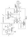
- FIG. 1illustrates a portion of a conventional CMOS imager 10 .
- the illustrated imager 10includes a pixel 20 , one of many that are in a pixel array (not shown), connected to a column sample and hold circuit 40 by a pixel output line 32 .
- the imager 10also includes a readout programmable gain amplifier (PGA) 70 and an analog-to-digital converter (ADC) 80 .
- PGAreadout programmable gain amplifier
- ADCanalog-to-digital converter
- the illustrated pixel 20includes a photosensor 22 (e.g., a pinned photodiode, photogate, etc.), transfer transistor 24 , floating diffusion region FD, reset transistor 26 , source follower transistor 28 and row select transistor 30 .
- FIG. 1also illustrates parasitic capacitance Cp 1 associated with the floating diffusion region FD and the pixel's 20 substrate.
- the photosensor 22is connected to the floating diffusion region FD by the transfer transistor 24 when the transfer transistor 24 is activated by a transfer control signal TX.
- the reset transistor 26is connected between the floating diffusion region FD and an array pixel supply voltage Vaa-pix.
- a reset control signal RSTis used to activate the reset transistor 26 , which resets the floating diffusion region FD (as is known in the art).
- the source follower transistor 28has its gate connected to the floating diffusion region FD and is connected between the array pixel supply voltage Vaa-pix and the row select transistor 30 .
- the source follower transistor 28converts the stored charge at the floating diffusion region FD into an electrical output voltage signal.
- the row select transistor 30is controllable by a row select signal SELECT for selectively connecting the source follower transistor 28 and its output voltage signal to the pixel output line 32 .
- the column sample and hold circuit 40includes a bias transistor 56 , controlled by a control voltage Vln_bias, that is used to bias the pixel output line 32 .
- the pixel output line 32is also connected to a first capacitor 44 thru a sample and hold reset signal switch 42 .
- the sample and hold reset signal switch 42is controlled by the sample and hold reset control signal SAMPLE_RESET.
- the pixel output line 32is also connected to a second capacitor 54 thru a sample and hold pixel signal switch 52 .
- the sample and hold pixel signal switch 52is controlled by the sample and hold pixel control signal SAMPLE_SIGNAL.
- the switches 42 , 52are typically MOSFET transistors.
- a second terminal of the first capacitor 44is connected to the amplifier 70 via a first column select switch 50 , which is controlled by a column select signal COLUMN_SELECT.
- the second terminal of the first capacitor 44is also connected to a clamping voltage VCL via a first clamping switch 46 .
- the second terminal of the second capacitor 54is connected to the amplifier 70 by a second column select switch 60 , which is controlled by the column select signal COLUMN_SELECT.
- the second terminal of the second capacitor 54is also connected to the clamping voltage VCL by a second clamping switch 48 .
- the clamping switches 46 , 48are controlled by a clamping control signal CLAMP.
- CLAMPclamping control signal
- the clamping voltage VCLis used to place a charge on the two capacitors 44 , 54 when it is desired to store the reset and pixel signals, respectively (when the appropriate sample and hold control signals SAMPLE_RESET, SAMPLE_SIGNAL are also generated).
- the row select signal SELECTis driven high, which activates the row select transistor 30 .
- the row select transistor 30connects the source follower transistor 28 to the pixel output line 32 .
- the clamping control signal CLAMPis then driven high to activate the clamping switches 46 , 48 , allowing the clamping voltage VCL to be applied to the second terminal of the sample and hold capacitors 44 , 54 .
- the reset signal RSTis then pulsed to activate the reset transistor 26 , which resets the floating diffusion region FD.
- the signal on the floating diffusion region FDis then sampled when the sample and hold reset control signal SAMPLE_RESET is pulsed.
- the first capacitor 44stores the pixel reset signal V rst .
- the transfer transistor control signal TXis pulsed, causing charge from the photosensor 22 to be transferred to the floating diffusion region FD.
- the signal on the floating diffusion region FDis sampled when the sample and hold pixel control signal SAMPLE_SIGNAL is pulsed.
- the second capacitor 54stores a pixel image signal V sig .
- a differential signal(V rst -V sig ) is produced by the differential amplifier 70 .
- the differential signalis digitized by the analog-to-digital converter 80 .
- the analog-to-digital converter 80supplies the digitized pixel signals to an image processor (not shown), which forms a digital image output.
- the pixel readout circuitryis designed to be fully differential to suppress noise (substrate or power supply noise), which could create undesirable image artifacts (e.g., flickering pixels, grainy still images).
- the readout circuitry for the illustrated four transistor (“4T”) pixel, and known three transistor (“3T”) pixelsis single ended.
- any noise on the substrate ground or clamp voltageis inadvertently stored on the sampling capacitors 44 , 54 .
- FIG 3illustrates portions of the imager 10 that are subject to substrate noise (e.g., at the floating diffusion region FD in the pixel 20 (arrow A) and the bias transistor 56 in the sample and hold circuitry 40 (arrow B)) and noise on the clamp voltage VCL (e.g., at clamping switches 46 , 48 (arrow C)).
- substrate noisee.g., at the floating diffusion region FD in the pixel 20 (arrow A) and the bias transistor 56 in the sample and hold circuitry 40 (arrow B)
- VCLclamp voltage
- the random noisewill be different between the two samples.
- Some components of the noiseare common to all the pixels in a particular row (e.g., substrate noise that is picked up by the floating diffusion region FD and the clamp voltage noise).
- the noiseappears as horizontal lines in the image that are superimposed on top of the actual image. This common noise is referred to as “row-wise noise” because the noise for the entire row is correlated.
- the inventionprovides an imager that mitigates the presence of row-wise noise in acquired images.
- the inventionprovides an imager that mitigates the presence of row-wise noise in acquired images while also overcoming adverse effects attributable to warm and hot pixels.
- Various exemplary embodiments of the inventionprovide an imager having optically and electrically black reference pixels in each row of the imager's pixel array. Since the reference pixels of each row experience the same row-wise noise as active imaging pixels in the associated row, the signals from the reference pixels are used to cancel out row-wise noise from the row of imaging pixels.
- the reference pixelsare designed such that their photosensors are physically or effectively removed from the row-wise noise correction, thus rendering them electrically black or dark. As such, the reference pixels can be used to provide row-wise noise correction without the adverse effects of warm and hot pixels.
- FIG. 1is a diagram of a portion of a typical CMOS imager
- FIG. 2is a timing diagram of the operation of the FIG. 1 imager
- FIG. 3is a diagram illustrating noise sources in the FIG. 1 imager
- FIG. 4is a diagram of a portion of a CMOS imager having row-wise noise correction
- FIG. 5illustrates possible causes of warm and hot pixels in a reference pixel used in the FIG. 4 imager
- FIG. 6illustrates an exemplary reference pixel, used in the FIG. 4 imager, constructed in accordance with an exemplary embodiment of the invention
- FIG. 7illustrates an exemplary potential diagram for the exemplary pixel of FIG. 6 ;
- FIG. 8illustrates an exemplary top down view of the exemplary pixel of FIG. 6 ;
- FIG. 9illustrates an exemplary cross-sectional view of the exemplary pixel of FIG. 6 ;
- FIG. 10illustrates another exemplary reference pixel, used in the FIG. 4 imager, constructed in accordance with another exemplary embodiment of the invention.
- FIG. 11illustrates another exemplary reference pixel, used in the FIG. 4 imager, constructed in accordance with another exemplary embodiment of the invention.
- FIG. 12shows a processor system incorporating at least one imaging device constructed in accordance with an embodiment of the invention.
- FIG. 4shows of a portion of a CMOS imager 110 described in application Ser. No. 10/834,844, filed Apr. 30, 2004, which is hereby incorporated by reference in its entirety.
- the imager 110includes a pixel array 112 comprised of active imaging pixels 120 .
- the top portion of the array 112contains light shielded optically black (“OB”) pixels 120 OB .
- the array 112contains reference pixels 120 REF , which are light shielded optically black pixels, associated with each row of active pixels 120 .
- the OB and reference pixels 120 OB , 120 REFare discussed below in more detail. According to application Ser. No.
- the imaging, OB and reference pixels 120 , 120 OB , 120 REFmay each have the construction of the 4T pixel illustrated in FIG. 1 , or other types of pixel architectures suitable for use in a CMOS imager (e.g., 3T, 5T, etc.).
- the illustrated imager 110also contains a control circuit 190 , row decoder 192 , row controller/driver 194 , column S/H and readout circuitry 198 , a column decoder 196 , readout/PGA gain amplifier 170 , analog-to-digital converter 180 and an image processor 185 .
- Row lines RL connected to the pixels 120 , 120 OB , 120 REF of the array 112are selectively activated by the row driver 194 in response to the row address decoder 192 .
- Column select lines CSare selectively activated by the column S/H and readout circuit 198 in response to the column address decoder 196 .
- Pixel output lines for each column in the arrayare also connected to the column S/H and readout circuitry 198 , but are not shown in FIG. 4 .
- the CMOS imager 110is operated by the control circuit 190 , which controls the decoders 192 , 196 for selecting the appropriate row and column lines for pixel readout.
- the control circuit 190also controls the row control/driver and column S/H and readout circuitry 192 , 198 , which apply driving voltages to the drive transistors of the selected row and column lines.
- the control circuit 190also controls other signals (e.g., SAMPLE_RESET and SAMPLE_SIGNAL illustrated in FIG. 1 ) needed by the column S/H and readout circuitry 198 to readout, sample, hold and output reset and pixel signals.
- the sample and hold portion of the column S/H and readout circuitry 198reads a pixel reset signal V rst and a pixel image signal V sig for selected pixels.
- a differential signal(V rst -V sig ) is produced by differential amplifier 170 for each pixel and is digitized by analog-to-digital converter 180 .
- the analog-to-digital converter 180supplies the digitized pixel signals to the image processor 185 , which forms a digital image output.
- the OB pixels 120 OB located at the top of the pixel array 112are light shielded and comprise multiple rows and columns of optically black pixels. It is desirable that each column of the array 112 be connected to multiple rows of OB pixels 120 OB .
- the OB pixels 120 OBare used for calibration purposes to compute a dark level pedestal, which is used as a minimum black signal reference point during calibration. An average of the signal levels of the OB pixels 120 OB is used to set an analog pedestal level to a target range.
- the reference pixels 120 REFare also light shielded.
- One technique for shielding the reference pixels 120 REFis to cover them with metal. Because the reference pixels 120 REF are light shielded, the only signal that should be read from them should be dark or optically black signals.
- the reference pixels 120 REFexperience the same row-wise noise superimposed on their signals that is experienced by the active pixels 120 within the same row. Thus, the row-wise noise for each row in the array 112 can be determined from the corresponding reference pixels 120 REF . Each row's associated row-wise noise can therefore be removed from the signals output by its associated active pixels 120 .
- a detailed explanation of how the reference pixels 120 REF are used to mitigate row-wise noiseis found in application Ser. No. 10/834,844.
- a warm pixelis a pixel that appears a little brighter than dark when it is supposed to be completely dark or optically black.
- a hot pixelis a pixel that appears bright when it is supposed to be completely dark/black.
- Warm and hot pixelsare typically caused by process defects such as e.g., silicon defects, metallic contamination, stress, etc.
- the row-noise correction schemecan introduce a correction offset that is not attributable to the row-wise noise. That is, the values of the warm or hot reference pixels 120 REF throws off the row-wise noise compensation average discussed above; this improper average will cause an incorrect compensation/offset to be applied to the image pixels 120 in that row, causing the entire row of image pixels 120 to fail.
- FIG. 5illustrates an example of a pixel 20 that could be used as a reference pixel 120 REF by covering its photosensor 22 with a metallic or other opaque shield SH.
- FIG. 5it is possible that light LD can get underneath the shield SH and strike the photosensor 22 directly, causing unwanted photons to reach the photosensor 22 .
- Another undesirable phenomenonoccurs when infrared light L IR travels through the pixel's substrate, is reflected from the bottom of the substrate and strikes the photosensor 22 .
- Another undesirable phenomenonknown as blooming L BL , occurs when stray electrons travel to the photosensor 22 from an adjacent pixel's photosensor 22 ′ that may or may not be exposed to light. All of these phenomena cause photons and/or electrons to reach the photosensor 22 of the reference pixel 120 REF , which is supposed to be electrically and/or optically black. These non-black reference pixels 120 REF will cause the row of imaging pixels 120 to fail when row-wise noise correction is applied to them (as described above).
- the present inventionprovides a method and reference pixel structures for providing row-wise noise correction that will not suffer from warm and/or hot pixel phenomena and mitigates against the row failures attributable to warm and hot reference pixels.
- the inventorshave determined that row-wise noise is potentially caused by noise in the readout circuitry, row drivers or correlated double sampling process, but is not directly related to the photosensor.
- the photosensorwhich is the main source of warm and hot pixels, is effectively (and sometimes physically) removed from the row-wise noise correction scheme of the invention as is described below in more detail.
- FIG. 6illustrates a reference pixel 220 REF constructed in accordance with a first exemplary embodiment of the invention.
- a plurality of the illustrated reference pixels 220 REFreplace the plurality of reference pixels 120 REF in the imager 110 illustrated in FIG. 4 .
- the reference pixels 220 REFare covered by a light shield and are positioned on the periphery of the array of imaging pixels 120 .
- Each reference pixel 220 REF of the illustrated embodimentincludes a photosensor 122 (illustrated as a pinned photodiode), transfer transistor 124 , floating diffusion region FD, reset transistor 126 , source follower transistor 128 and a row select transistor 130 .
- the reference pixel 220 REFis essentially the same as the pixel 20 ( FIG. 1 ), which is covered by a light shield to form the reference pixel 120 REF ( FIG. 4 ).
- the photosensor 122is connected to the floating diffusion region FD by the transfer transistor 124 when the transfer transistor 124 is activated by a transfer control signal TX.
- the reset transistor 126is connected between the floating diffusion region FD and an array pixel supply voltage Vaa-pix.
- a reset control signal RSTis used to activate the reset transistor 126 , which resets the floating diffusion region FD.
- the source follower transistor 128has its gate connected to the floating diffusion region FD and is connected between the array pixel supply voltage Vaa-pix and the row select transistor 130 .
- the source follower transistor 128converts the stored charge at the floating diffusion region FD into an electrical output voltage signal.
- the row select transistor 130is controllable by a row select signal SELECT for selectively connecting the source follower transistor 128 and its output voltage signal to a pixel output line 132 .
- the reference pixel 220 REF of the illustrated embodimentdiffers from the typical reference pixel 120 REF in that the photosensor 122 of the illustrated embodiment is tied to the array pixel supply voltage Vaa-pix. That is, the photosensor 122 contains a contact (e.g., contact 214 illustrated in FIG. 9 ) connected to the array pixel supply voltage Vaa-pix. As such, in operation, the reference pixel 220 REF is depleted of electrons, and always appears electrically black/dark. In addition, during the operation of the reference pixels 220 REF , any dark current electrons as well as any electrons generated by absorbed photons generated in the photosensor 122 (by e.g., the phenomena described above with respect to FIG.
- the illustrated photosensor 122is a pinned photodiode.
- the inventionis described by way of example with use of a pinned photodiode photosensor 122 . It should be noted that the invention is not limited to a pinned photodiode photosensor 122 . The invention can be used with non-pinned photodiodes, photogates, photoconductors or other photosensitive elements.
- FIG. 7illustrates a potential diagram for the reference pixel 220 REF using a pinned photodiode photosensor 122 .
- the pinned photodiodehas a pinned voltage Vpin.
- the array pixel supply voltage Vaa-pixis also shown. Is should be appreciated that the photosensor 122 could be connected to any voltage and is not limited solely to the array pixel supply voltage Vaa-pix. For example, if the photosensor 122 is a pinned photodiode, the voltage connected to the photodiode could be any voltage greater than the pinning voltage Vpin, but less than or equal to the maximum operating voltage of the part.
- the voltage connected to the photosensor 122must be greater than or equal to the reset level of the photodiode (i.e., not limited to the array pixel supply voltage Vaa-pix).
- the reset level of the photodiodei.e., not limited to the array pixel supply voltage Vaa-pix.
- the necessary isolationcould be achieved by positioning the contact 214 connected to the array pixel supply voltage Vaa-pix a sufficient distance D from the transfer transistor gate 124 ′. It should be noted that the exact distance D from the transfer transistor gate 124 ′ is dependent upon the implant conditions of the photosensor and the transfer transistor 124 .
- FIG. 8also shows the reset transistor gate 126 ′, source follower gate 128 ′ and the row select transistor gate 130 ′.
- a high threshold voltage transistorcould be used as the transfer transistor 124 .
- the threshold voltage of the transfer transistor 124needs to be higher than the difference between the FD reset voltage and the array pixel supply voltage Vaa-pix (or the voltage that is connected to the photosensor 122 if Vaa-pix is not used).
- FIG. 9is a cross-sectional view of the reference pixel 220 REF taken along line A′-A′ of FIG. 8 , which illustrates one embodiment of connecting the array pixel supply voltage Vaa-pix to the photosensor 122 (implemented as a pinned photodiode).
- the pinned photodiode photosensor 122contains an n ⁇ accumulation region 206 underneath two p+ surface regions 204 , 210 .
- a n+ implanted region 208is also provided to make the best possible connection between the n ⁇ accumulation region 206 and the contact 214 .
- the contact 214is connected to a metal line 216 , which is connected to the array pixel supply voltage Vaa-pix.
- FIG. 9also shows the transfer gate 124 ′ connected between the photosensor 122 and the floating diffusion region FD (shown as an n-type region within a p ⁇ substrate).
- STI isolation regions 202 , 212are also shown, but any type of isolation technique can be used.
- FIG. 10illustrates a reference pixel 320 REF constructed in accordance with another embodiment of the invention.
- a plurality of the illustrated reference pixels 320 REFreplace the plurality of reference pixels 120 REF in the imager 110 illustrated in FIG. 4 .
- the reference pixel 320 REFcontains a source follower transistor 326 and a row select transistor 330 , but does not contain a photosensor, transfer transistor or floating diffusion region.
- the source follower transistor 328has its gate and one of its source/drain terminals connected to the array pixel supply voltage Vaa-pix. With this configuration, a voltage corresponding to the electrically dark condition is always output on the column line 332 when the row select transistor 330 is activated by the SELECT signal.
- the voltage on the source/drain terminal and gate of the source follower transistor 328could be any voltage as long as the pixel reset signal Vrst and the pixel image signal Vsig are identical, resulting in an electrically dark condition.
- the illustrated embodimentdoes not allow for correlated double sampling.
- the reference pixel 320 REFwill alleviate most row-wise noise, but not the noise attributable to correlated double sampling (if any).
- the above-illustrated embodimentsmay be modified to provide other means of “removing” the photosensor from the row-wise noise correction calculation.
- a plurality of the illustrated reference pixels 420 REFreplace the plurality of reference pixels 120 REF in the imager 110 illustrated in FIG. 4 .
- a reset of the floating diffusion region FDwill cause a reset of the photosensor 122 as well. This reset removes any electrons that could result in a warm or hot reference pixel 420 REF .
- the typical reference pixel 120 REFis used, but operated in a manner that effectively removes the photosensor 22 ( FIG. 5 ) from the row-wise noise correction calculations.
- both the transfer gate and reset gateare activated such that the photosensor is put into a reset state prior to readout.
- This alternativerequires separate pixel control signals for the reference pixels 120 REF and the imaging pixels 120 .
- global pixel control signalscan be used for each row since the reference pixel 220 REF and the imaging pixels 120 are operated in the same manner.
- the typical reference pixel 120 REFis used, but the n ⁇ accumulation region 206 implants from the photosensor 22 are removed or blocked from the reference pixel 120 REF .
- This alternativephysically removes the photosensor 22 from the equation thus preventing the formation of a warm or hot reference pixel.
- the typical reference pixel 120 REFis used, but operated in another manner that effectively removes the photosensor 22 ( FIG. 5 ) from the row-wise noise correction calculations.
- the transfer transistor 124 within the reference pixel 120 REFis never activated, which means that the charges from the photosensor 122 cannot be transferred to the floating diffusion region FD.
- reference pixels 220 REF , 320 REF , 420 REFcould be on either or both sides of the pixel array 112 ( FIG. 4 ).
- FIG. 12shows system 700 , a typical processor system modified to include an imaging device 708 constructed in accordance with an embodiment of the invention (i.e., imager 110 of FIG. 4 having reference pixels of the invention e.g., reference pixels 220 REF , 320 REF , 420 REF ).
- the processor-based system 700is exemplary of a system having digital circuits that could include image sensor devices. Without being limiting, such a system could include a computer system, camera system, scanner, machine vision, vehicle navigation, video phone, surveillance system, auto focus system, star tracker system, motion detection system, image stabilization system, and data compression system.
- System 700for example a camera system, generally comprises a central processing unit (CPU) 702 , such as a microprocessor, that communicates with an input/output (I/O) device 706 over a bus 704 .
- Imaging device 708also communicates with the CPU 702 over the bus 704 .
- the processor-based system 700also includes random access memory (RAM) 710 , and can include removable memory 715 , such as flash memory, which also communicate with the CPU 702 over the bus 704 .
- the imaging device 708may be combined with a processor, such as a CPU, digital signal processor, or microprocessor, with or without memory storage on a single integrated circuit or on a different chip than the processor.
- a method of manufacturing an imaging devicecomprises the acts of fabricating an array of imaging pixels, said array being organized into a plurality of rows and columns, and fabricating a plurality of reference pixels, said plurality of reference pixels being arranged into a plurality of rows, each row of reference pixels corresponding to a respective row of imaging pixels within said array, each reference pixel being configured to output electrically black signals to be used in row-wise noise correction of signals from the imaging pixels from its associated row.
- the ability to reset the photosensoris not limited to the above-described embodiments.
- another transistormay be directly connected to the photosensor of the reference pixels.
- the photosensorwill be reset by an appropriate voltage connected to a source/drain terminal of the additional transistor.
- the inventionhas been described as being part of a CMOS imager, it should be noted that the invention applies to any imager that uses row-wise noise correction based on dark or optically black reference pixels. That is, the invention also applies to CCD imagers.
Landscapes
- Engineering & Computer Science (AREA)
- Multimedia (AREA)
- Signal Processing (AREA)
- Solid State Image Pick-Up Elements (AREA)
- Transforming Light Signals Into Electric Signals (AREA)
Abstract
Description
Claims (26)
Priority Applications (2)
| Application Number | Priority Date | Filing Date | Title |
|---|---|---|---|
| US11/066,781US7701493B2 (en) | 2005-02-28 | 2005-02-28 | Imager row-wise noise correction |
| US12/573,985US7852385B2 (en) | 2005-02-28 | 2009-10-06 | Imager row-wise noise correction |
Applications Claiming Priority (1)
| Application Number | Priority Date | Filing Date | Title |
|---|---|---|---|
| US11/066,781US7701493B2 (en) | 2005-02-28 | 2005-02-28 | Imager row-wise noise correction |
Related Child Applications (1)
| Application Number | Title | Priority Date | Filing Date |
|---|---|---|---|
| US12/573,985DivisionUS7852385B2 (en) | 2005-02-28 | 2009-10-06 | Imager row-wise noise correction |
Publications (2)
| Publication Number | Publication Date |
|---|---|
| US20060192864A1 US20060192864A1 (en) | 2006-08-31 |
| US7701493B2true US7701493B2 (en) | 2010-04-20 |
Family
ID=36931621
Family Applications (2)
| Application Number | Title | Priority Date | Filing Date |
|---|---|---|---|
| US11/066,781Active2028-01-04US7701493B2 (en) | 2005-02-28 | 2005-02-28 | Imager row-wise noise correction |
| US12/573,985Expired - LifetimeUS7852385B2 (en) | 2005-02-28 | 2009-10-06 | Imager row-wise noise correction |
Family Applications After (1)
| Application Number | Title | Priority Date | Filing Date |
|---|---|---|---|
| US12/573,985Expired - LifetimeUS7852385B2 (en) | 2005-02-28 | 2009-10-06 | Imager row-wise noise correction |
Country Status (1)
| Country | Link |
|---|---|
| US (2) | US7701493B2 (en) |
Cited By (20)
| Publication number | Priority date | Publication date | Assignee | Title |
|---|---|---|---|---|
| US20080239124A1 (en)* | 2007-03-30 | 2008-10-02 | Sony Corporation | Solid-state imaging device, signal processing method of solid-state imaging device and imaging apparatus |
| US20090109314A1 (en)* | 2005-03-18 | 2009-04-30 | Canon Kabushiki Kaisha | Solid state image pickup device and camera |
| US20090273691A1 (en)* | 2008-05-02 | 2009-11-05 | Yaowu Mo | Method and apparatus providing analog row noise correction and hot pixel filtering |
| US20100079632A1 (en)* | 2008-09-26 | 2010-04-01 | Tom Walschap | Correlated double sampling pixel |
| US20110205405A1 (en)* | 2004-06-30 | 2011-08-25 | Ilia Ovsiannikov | Shielding black reference pixels in image sensors |
| US20110317055A1 (en)* | 2010-06-29 | 2011-12-29 | Kabushiki Kaisha Toshiba | Solid-state imaging device, camera module, and imaging method |
| US20120312967A1 (en)* | 2011-06-10 | 2012-12-13 | Yannick De Wit | Pixel and method |
| US8946783B2 (en) | 2012-06-18 | 2015-02-03 | Samsung Electronics Co., Ltd. | Image sensors having reduced dark level differences |
| US20150042847A1 (en)* | 2012-04-20 | 2015-02-12 | Daisuke HOHJOH | Imaging device and image processing method |
| US9362326B2 (en)* | 2012-08-22 | 2016-06-07 | Canon Kabushiki Kaisha | Image capturing apparatus and control method therefor |
| US10645348B2 (en) | 2018-07-07 | 2020-05-05 | Sensors Unlimited, Inc. | Data communication between image sensors and image displays |
| US10742913B2 (en) | 2018-08-08 | 2020-08-11 | N2 Imaging Systems, LLC | Shutterless calibration |
| US10753709B2 (en) | 2018-05-17 | 2020-08-25 | Sensors Unlimited, Inc. | Tactical rails, tactical rail systems, and firearm assemblies having tactical rails |
| US10796860B2 (en) | 2018-12-12 | 2020-10-06 | N2 Imaging Systems, LLC | Hermetically sealed over-molded button assembly |
| US10801813B2 (en) | 2018-11-07 | 2020-10-13 | N2 Imaging Systems, LLC | Adjustable-power data rail on a digital weapon sight |
| US10921578B2 (en) | 2018-09-07 | 2021-02-16 | Sensors Unlimited, Inc. | Eyecups for optics |
| US11079202B2 (en) | 2018-07-07 | 2021-08-03 | Sensors Unlimited, Inc. | Boresighting peripherals to digital weapon sights |
| US11122698B2 (en) | 2018-11-06 | 2021-09-14 | N2 Imaging Systems, LLC | Low stress electronic board retainers and assemblies |
| US11143838B2 (en) | 2019-01-08 | 2021-10-12 | N2 Imaging Systems, LLC | Optical element retainers |
| US11162763B2 (en) | 2015-11-03 | 2021-11-02 | N2 Imaging Systems, LLC | Non-contact optical connections for firearm accessories |
Families Citing this family (31)
| Publication number | Priority date | Publication date | Assignee | Title |
|---|---|---|---|---|
| US7508430B1 (en)* | 2005-02-18 | 2009-03-24 | Magnachip Semiconductor, Ltd. | Method for locally reducing row noise |
| US7564489B1 (en)* | 2005-02-18 | 2009-07-21 | Crosstek Capital, LLC | Method for reducing row noise with dark pixel data |
| JP4771535B2 (en)* | 2005-05-17 | 2011-09-14 | キヤノン株式会社 | Imaging apparatus and control method |
| US20070236590A1 (en)* | 2006-03-31 | 2007-10-11 | Cypress Semiconductor Corporation | Output auto-zero for CMOS active pixel sensors |
| JP4976765B2 (en)* | 2006-07-07 | 2012-07-18 | ルネサスエレクトロニクス株式会社 | Solid-state imaging device |
| US7545418B2 (en)* | 2006-07-17 | 2009-06-09 | Jeffery Steven Beck | Image sensor device having improved noise suppression capability and a method for supressing noise in an image sensor device |
| JP4185949B2 (en) | 2006-08-08 | 2008-11-26 | キヤノン株式会社 | Photoelectric conversion device and imaging device |
| KR100784387B1 (en)* | 2006-11-06 | 2007-12-11 | 삼성전자주식회사 | Image sensor and its formation method |
| US20080170228A1 (en)* | 2007-01-17 | 2008-07-17 | Micron Technology, Inc. | Method and apparatus for wafer level calibration of imaging sensors |
| US20080239111A1 (en)* | 2007-03-26 | 2008-10-02 | Micron Technology, Inc. | Method and appratus for dark current compensation of imaging sensors |
| US8310569B2 (en)* | 2007-05-21 | 2012-11-13 | Aptina Imaging Corporation | Suppression of row-wise noise in CMOS image sensors |
| JP2009038531A (en)* | 2007-07-31 | 2009-02-19 | Panasonic Corp | Solid-state imaging device and driving method thereof |
| US20090040351A1 (en)* | 2007-08-09 | 2009-02-12 | Micron Technology, Inc. | Method and apparatus for reducing noise in a pixel array |
| US7991239B2 (en)* | 2007-08-29 | 2011-08-02 | Aptina Imaging Corporation | Methods, systems and apparatuses for imager row-wise noise correction |
| JP2009089029A (en)* | 2007-09-28 | 2009-04-23 | Fujifilm Corp | CCD type solid-state imaging device |
| US7924330B2 (en)* | 2007-12-20 | 2011-04-12 | Aptina Imaging Corporation | Methods and apparatuses for double sided dark reference pixel row-wise dark level non-uniformity compensation in image signals |
| EP4020976A1 (en)* | 2008-04-07 | 2022-06-29 | Cmosis NV | Pixel array |
| US7889256B2 (en)* | 2008-06-11 | 2011-02-15 | Aptina Imaging Corporation | Method and apparatus for reducing temporal row-wise noise in imagers |
| US8130289B2 (en)* | 2008-09-25 | 2012-03-06 | Aptima Imaging Corporation | System, method, and apparatus for correction of dark current error in semiconductor imaging devices |
| US20100252717A1 (en)* | 2008-09-29 | 2010-10-07 | Benoit Dupont | Active-pixel sensor |
| KR101566406B1 (en)* | 2008-10-22 | 2015-11-16 | 삼성전자주식회사 | Image sensor failure detection method and image sensor using the method |
| JP5455798B2 (en)* | 2009-07-16 | 2014-03-26 | キヤノン株式会社 | Image processing device |
| DE102010001918B4 (en)* | 2010-02-15 | 2017-05-18 | Robert Bosch Gmbh | image converter |
| US8836835B2 (en) | 2010-10-04 | 2014-09-16 | International Business Machines Corporation | Pixel sensor cell with hold node for leakage cancellation and methods of manufacture and design structure |
| JP5933219B2 (en)* | 2011-10-21 | 2016-06-08 | オリンパス株式会社 | Solid-state imaging device |
| CN103259985B (en)* | 2013-05-17 | 2016-08-17 | 昆山锐芯微电子有限公司 | Cmos image sensor, pixel cell and control method thereof |
| US10154213B2 (en) | 2016-09-28 | 2018-12-11 | Semiconductor Components Industries, Llc | Image sensors having dark pixels |
| CN109285854A (en)* | 2018-11-20 | 2019-01-29 | 德淮半导体有限公司 | Image sensor, method for manufacturing the same, and imaging device |
| CN111464765B (en)* | 2020-04-15 | 2022-08-26 | 锐芯微电子股份有限公司 | Fully differential pixel readout circuit, pixel circuit, and pixel data readout method |
| US11678084B2 (en) | 2020-10-19 | 2023-06-13 | Semiconductor Components Industries, Llc | Image sensors with adaptive filtering for row noise mitigation |
| US12174071B2 (en)* | 2022-05-13 | 2024-12-24 | Verity Instruments, Inc. | System, apparatus, and method for improved background correction and calibration of optical devices |
Citations (22)
| Publication number | Priority date | Publication date | Assignee | Title |
|---|---|---|---|---|
| US5471515A (en) | 1994-01-28 | 1995-11-28 | California Institute Of Technology | Active pixel sensor with intra-pixel charge transfer |
| US5625210A (en)* | 1995-04-13 | 1997-04-29 | Eastman Kodak Company | Active pixel sensor integrated with a pinned photodiode |
| US5903021A (en)* | 1997-01-17 | 1999-05-11 | Eastman Kodak Company | Partially pinned photodiode for solid state image sensors |
| US6140630A (en) | 1998-10-14 | 2000-10-31 | Micron Technology, Inc. | Vcc pump for CMOS imagers |
| US6204524B1 (en) | 1999-07-14 | 2001-03-20 | Micron Technology, Inc. | CMOS imager with storage capacitor |
| US6310366B1 (en) | 1999-06-16 | 2001-10-30 | Micron Technology, Inc. | Retrograde well structure for a CMOS imager |
| US6320617B1 (en)* | 1995-11-07 | 2001-11-20 | Eastman Kodak Company | CMOS active pixel sensor using a pinned photo diode |
| US6326652B1 (en) | 1999-06-18 | 2001-12-04 | Micron Technology, Inc., | CMOS imager with a self-aligned buried contact |
| US20010052574A1 (en)* | 2000-05-30 | 2001-12-20 | Susumu Kurosawa | MOS-based image sensor and method of forming black-level signal therefor |
| US6333205B1 (en) | 1999-08-16 | 2001-12-25 | Micron Technology, Inc. | CMOS imager with selectively silicided gates |
| US6376868B1 (en) | 1999-06-15 | 2002-04-23 | Micron Technology, Inc. | Multi-layered gate for a CMOS imager |
| US6388243B1 (en)* | 1999-03-01 | 2002-05-14 | Photobit Corporation | Active pixel sensor with fully-depleted buried photoreceptor |
| US6473124B1 (en) | 1998-04-23 | 2002-10-29 | Micron Technology, Inc. | RAM line storage for fixed pattern noise correction |
| US6529242B1 (en) | 1998-03-11 | 2003-03-04 | Micron Technology, Inc. | Look ahead shutter pointer allowing real time exposure control |
| US20030052982A1 (en) | 2001-09-20 | 2003-03-20 | Yuen-Shung Chieh | Method for reducing coherent row-wise and column-wise fixed pattern noise in CMOS image sensors |
| US6566697B1 (en)* | 2000-11-28 | 2003-05-20 | Dalsa, Inc. | Pinned photodiode five transistor pixel |
| US6781169B2 (en)* | 2001-02-12 | 2004-08-24 | Stmicroelectronics S.A. | Photodetector with three transistors |
| US6781171B2 (en)* | 2002-07-19 | 2004-08-24 | Dongbu Electronics Co., Ltd. | Pinned photodiode for a CMOS image sensor and fabricating method thereof |
| US20040263641A1 (en)* | 2003-05-23 | 2004-12-30 | Nikon Corporation | Signal processing unit for correcting shading of image signal, and electronic camera |
| US20050243194A1 (en)* | 2004-04-30 | 2005-11-03 | Eastman Kodak Company | Low noise sample and hold circuit for image sensors |
| US20060038207A1 (en)* | 2004-08-19 | 2006-02-23 | Hong Sungkwon C | Wide dynamic range sensor having a pinned diode with multiple pinned voltages |
| US7245322B2 (en)* | 2003-01-17 | 2007-07-17 | Fujifilm Corporation | Imaging apparatus |
Family Cites Families (1)
| Publication number | Priority date | Publication date | Assignee | Title |
|---|---|---|---|---|
| US52982A (en)* | 1866-03-06 | Improvement in steam-superheaters |
- 2005
- 2005-02-28USUS11/066,781patent/US7701493B2/enactiveActive
- 2009
- 2009-10-06USUS12/573,985patent/US7852385B2/ennot_activeExpired - Lifetime
Patent Citations (25)
| Publication number | Priority date | Publication date | Assignee | Title |
|---|---|---|---|---|
| US5471515A (en) | 1994-01-28 | 1995-11-28 | California Institute Of Technology | Active pixel sensor with intra-pixel charge transfer |
| US6100551A (en)* | 1995-04-13 | 2000-08-08 | Eastman Kodak Company | Active pixel sensor integrated with a pinned photodiode |
| US5625210A (en)* | 1995-04-13 | 1997-04-29 | Eastman Kodak Company | Active pixel sensor integrated with a pinned photodiode |
| US5841159A (en)* | 1995-04-13 | 1998-11-24 | Eastman Kodak Company | Active pixel sensor integrated with a photocapacitor |
| US6320617B1 (en)* | 1995-11-07 | 2001-11-20 | Eastman Kodak Company | CMOS active pixel sensor using a pinned photo diode |
| US5903021A (en)* | 1997-01-17 | 1999-05-11 | Eastman Kodak Company | Partially pinned photodiode for solid state image sensors |
| US6051447A (en)* | 1997-01-17 | 2000-04-18 | Eastman Kodak Company | Partially pinned photodiode for solid state image sensors |
| US6529242B1 (en) | 1998-03-11 | 2003-03-04 | Micron Technology, Inc. | Look ahead shutter pointer allowing real time exposure control |
| US6473124B1 (en) | 1998-04-23 | 2002-10-29 | Micron Technology, Inc. | RAM line storage for fixed pattern noise correction |
| US6140630A (en) | 1998-10-14 | 2000-10-31 | Micron Technology, Inc. | Vcc pump for CMOS imagers |
| US6388243B1 (en)* | 1999-03-01 | 2002-05-14 | Photobit Corporation | Active pixel sensor with fully-depleted buried photoreceptor |
| US6376868B1 (en) | 1999-06-15 | 2002-04-23 | Micron Technology, Inc. | Multi-layered gate for a CMOS imager |
| US6310366B1 (en) | 1999-06-16 | 2001-10-30 | Micron Technology, Inc. | Retrograde well structure for a CMOS imager |
| US6326652B1 (en) | 1999-06-18 | 2001-12-04 | Micron Technology, Inc., | CMOS imager with a self-aligned buried contact |
| US6204524B1 (en) | 1999-07-14 | 2001-03-20 | Micron Technology, Inc. | CMOS imager with storage capacitor |
| US6333205B1 (en) | 1999-08-16 | 2001-12-25 | Micron Technology, Inc. | CMOS imager with selectively silicided gates |
| US20010052574A1 (en)* | 2000-05-30 | 2001-12-20 | Susumu Kurosawa | MOS-based image sensor and method of forming black-level signal therefor |
| US6566697B1 (en)* | 2000-11-28 | 2003-05-20 | Dalsa, Inc. | Pinned photodiode five transistor pixel |
| US6781169B2 (en)* | 2001-02-12 | 2004-08-24 | Stmicroelectronics S.A. | Photodetector with three transistors |
| US20030052982A1 (en) | 2001-09-20 | 2003-03-20 | Yuen-Shung Chieh | Method for reducing coherent row-wise and column-wise fixed pattern noise in CMOS image sensors |
| US6781171B2 (en)* | 2002-07-19 | 2004-08-24 | Dongbu Electronics Co., Ltd. | Pinned photodiode for a CMOS image sensor and fabricating method thereof |
| US7245322B2 (en)* | 2003-01-17 | 2007-07-17 | Fujifilm Corporation | Imaging apparatus |
| US20040263641A1 (en)* | 2003-05-23 | 2004-12-30 | Nikon Corporation | Signal processing unit for correcting shading of image signal, and electronic camera |
| US20050243194A1 (en)* | 2004-04-30 | 2005-11-03 | Eastman Kodak Company | Low noise sample and hold circuit for image sensors |
| US20060038207A1 (en)* | 2004-08-19 | 2006-02-23 | Hong Sungkwon C | Wide dynamic range sensor having a pinned diode with multiple pinned voltages |
Cited By (30)
| Publication number | Priority date | Publication date | Assignee | Title |
|---|---|---|---|---|
| US20110205405A1 (en)* | 2004-06-30 | 2011-08-25 | Ilia Ovsiannikov | Shielding black reference pixels in image sensors |
| US8411174B2 (en)* | 2004-06-30 | 2013-04-02 | Micron Technology, Inc. | Shielding black reference pixels in image sensors |
| US8749675B2 (en) | 2005-03-18 | 2014-06-10 | Canon Kabushiki Kaisha | Solid state image pickup device and camera which can prevent color mixture |
| US20090109314A1 (en)* | 2005-03-18 | 2009-04-30 | Canon Kabushiki Kaisha | Solid state image pickup device and camera |
| US8896029B2 (en) | 2005-03-18 | 2014-11-25 | Canon Kabushiki Kaisha | Solid state image pickup device and camera |
| US8390708B2 (en)* | 2005-03-18 | 2013-03-05 | Canon Kabushiki Kaisha | Solid state image pickup device and camera utilizing carrier holding unit and floating diffusion region |
| US20080239124A1 (en)* | 2007-03-30 | 2008-10-02 | Sony Corporation | Solid-state imaging device, signal processing method of solid-state imaging device and imaging apparatus |
| US8264580B2 (en)* | 2007-03-30 | 2012-09-11 | Sony Corporation | Solid state imaging device, signal processing method of solid-state imaging device and imaging apparatus capable of removing vertical smears |
| US20090273691A1 (en)* | 2008-05-02 | 2009-11-05 | Yaowu Mo | Method and apparatus providing analog row noise correction and hot pixel filtering |
| US8077227B2 (en)* | 2008-05-02 | 2011-12-13 | Aptina Imaging Corporation | Method and apparatus providing analog row noise correction and hot pixel filtering |
| US20100079632A1 (en)* | 2008-09-26 | 2010-04-01 | Tom Walschap | Correlated double sampling pixel |
| US8059173B2 (en)* | 2008-09-26 | 2011-11-15 | On Semiconductor Trading Ltd. | Correlated double sampling pixel and method |
| US20110317055A1 (en)* | 2010-06-29 | 2011-12-29 | Kabushiki Kaisha Toshiba | Solid-state imaging device, camera module, and imaging method |
| US8451350B2 (en)* | 2010-06-29 | 2013-05-28 | Kabushiki Kaisha Toshiba | Solid-state imaging device, camera module, and imaging method |
| US20120312967A1 (en)* | 2011-06-10 | 2012-12-13 | Yannick De Wit | Pixel and method |
| US8987646B2 (en)* | 2011-06-10 | 2015-03-24 | Semiconductor Components Industries, Llc | Pixel and method |
| US20150042847A1 (en)* | 2012-04-20 | 2015-02-12 | Daisuke HOHJOH | Imaging device and image processing method |
| US9444979B2 (en)* | 2012-04-20 | 2016-09-13 | Ricoh Company, Ltd. | Imaging device and image processing method |
| US8946783B2 (en) | 2012-06-18 | 2015-02-03 | Samsung Electronics Co., Ltd. | Image sensors having reduced dark level differences |
| US9362326B2 (en)* | 2012-08-22 | 2016-06-07 | Canon Kabushiki Kaisha | Image capturing apparatus and control method therefor |
| US11162763B2 (en) | 2015-11-03 | 2021-11-02 | N2 Imaging Systems, LLC | Non-contact optical connections for firearm accessories |
| US10753709B2 (en) | 2018-05-17 | 2020-08-25 | Sensors Unlimited, Inc. | Tactical rails, tactical rail systems, and firearm assemblies having tactical rails |
| US11079202B2 (en) | 2018-07-07 | 2021-08-03 | Sensors Unlimited, Inc. | Boresighting peripherals to digital weapon sights |
| US10645348B2 (en) | 2018-07-07 | 2020-05-05 | Sensors Unlimited, Inc. | Data communication between image sensors and image displays |
| US10742913B2 (en) | 2018-08-08 | 2020-08-11 | N2 Imaging Systems, LLC | Shutterless calibration |
| US10921578B2 (en) | 2018-09-07 | 2021-02-16 | Sensors Unlimited, Inc. | Eyecups for optics |
| US11122698B2 (en) | 2018-11-06 | 2021-09-14 | N2 Imaging Systems, LLC | Low stress electronic board retainers and assemblies |
| US10801813B2 (en) | 2018-11-07 | 2020-10-13 | N2 Imaging Systems, LLC | Adjustable-power data rail on a digital weapon sight |
| US10796860B2 (en) | 2018-12-12 | 2020-10-06 | N2 Imaging Systems, LLC | Hermetically sealed over-molded button assembly |
| US11143838B2 (en) | 2019-01-08 | 2021-10-12 | N2 Imaging Systems, LLC | Optical element retainers |
Also Published As
| Publication number | Publication date |
|---|---|
| US20060192864A1 (en) | 2006-08-31 |
| US20100020213A1 (en) | 2010-01-28 |
| US7852385B2 (en) | 2010-12-14 |
Similar Documents
| Publication | Publication Date | Title |
|---|---|---|
| US7701493B2 (en) | Imager row-wise noise correction | |
| US11778343B2 (en) | Methods and circuitry for improving global shutter efficiency in backside illuminated high dynamic range image sensor pixels | |
| US8278131B2 (en) | Method and apparatus for dark current and blooming supression in 4T CMOS imager pixel | |
| US20080054320A1 (en) | Method, apparatus and system providing suppression of noise in a digital imager | |
| KR200492043Y1 (en) | Global shutter image sensor pixels having improved shutter efficiency | |
| US10536652B2 (en) | Image sensors with split photodiodes | |
| KR101531657B1 (en) | Solid-state imaging device, method of driving solid-state imaging device, and electronic device | |
| CN114173071B (en) | Dual conversion gain circuit with buried channel | |
| US7538304B2 (en) | Reducing noise in an imager by sampling signals with a plurality of capacitances connected to an output line | |
| US7825967B2 (en) | Column-wise clamp voltage driver for suppression of noise in an imager | |
| US8878264B2 (en) | Global shutter pixel with improved efficiency | |
| US20050243193A1 (en) | Suppression of row-wise noise in an imager | |
| US7800675B2 (en) | Method of operating a storage gate pixel | |
| US20080210986A1 (en) | Global shutter pixel with charge storage region | |
| US20070188642A1 (en) | Method and apparatus for dark current and hot pixel reduction in active pixel image sensors | |
| US20060243887A1 (en) | High dynamic range pixel amplifier | |
| JP2009505437A (en) | Method and apparatus for protecting correction pixels from false charges in an imager | |
| US7619671B2 (en) | Method, apparatus and system for charge injection suppression in active pixel sensors |
Legal Events
| Date | Code | Title | Description |
|---|---|---|---|
| AS | Assignment | Owner name:MICRON TECHNOLOGY, INC., IDAHO Free format text:ASSIGNMENT OF ASSIGNORS INTEREST;ASSIGNOR:MAURITZSON, RICHARD A.;REEL/FRAME:016338/0240 Effective date:20050228 Owner name:MICRON TECHNOLOGY, INC.,IDAHO Free format text:ASSIGNMENT OF ASSIGNORS INTEREST;ASSIGNOR:MAURITZSON, RICHARD A.;REEL/FRAME:016338/0240 Effective date:20050228 | |
| FEPP | Fee payment procedure | Free format text:PAYOR NUMBER ASSIGNED (ORIGINAL EVENT CODE: ASPN); ENTITY STATUS OF PATENT OWNER: LARGE ENTITY | |
| STCF | Information on status: patent grant | Free format text:PATENTED CASE | |
| FPAY | Fee payment | Year of fee payment:4 | |
| AS | Assignment | Owner name:U.S. BANK NATIONAL ASSOCIATION, AS COLLATERAL AGENT, CALIFORNIA Free format text:SECURITY INTEREST;ASSIGNOR:MICRON TECHNOLOGY, INC.;REEL/FRAME:038669/0001 Effective date:20160426 Owner name:U.S. BANK NATIONAL ASSOCIATION, AS COLLATERAL AGEN Free format text:SECURITY INTEREST;ASSIGNOR:MICRON TECHNOLOGY, INC.;REEL/FRAME:038669/0001 Effective date:20160426 | |
| AS | Assignment | Owner name:MORGAN STANLEY SENIOR FUNDING, INC., AS COLLATERAL AGENT, MARYLAND Free format text:PATENT SECURITY AGREEMENT;ASSIGNOR:MICRON TECHNOLOGY, INC.;REEL/FRAME:038954/0001 Effective date:20160426 Owner name:MORGAN STANLEY SENIOR FUNDING, INC., AS COLLATERAL Free format text:PATENT SECURITY AGREEMENT;ASSIGNOR:MICRON TECHNOLOGY, INC.;REEL/FRAME:038954/0001 Effective date:20160426 | |
| AS | Assignment | Owner name:U.S. BANK NATIONAL ASSOCIATION, AS COLLATERAL AGENT, CALIFORNIA Free format text:CORRECTIVE ASSIGNMENT TO CORRECT THE REPLACE ERRONEOUSLY FILED PATENT #7358718 WITH THE CORRECT PATENT #7358178 PREVIOUSLY RECORDED ON REEL 038669 FRAME 0001. ASSIGNOR(S) HEREBY CONFIRMS THE SECURITY INTEREST;ASSIGNOR:MICRON TECHNOLOGY, INC.;REEL/FRAME:043079/0001 Effective date:20160426 Owner name:U.S. BANK NATIONAL ASSOCIATION, AS COLLATERAL AGEN Free format text:CORRECTIVE ASSIGNMENT TO CORRECT THE REPLACE ERRONEOUSLY FILED PATENT #7358718 WITH THE CORRECT PATENT #7358178 PREVIOUSLY RECORDED ON REEL 038669 FRAME 0001. ASSIGNOR(S) HEREBY CONFIRMS THE SECURITY INTEREST;ASSIGNOR:MICRON TECHNOLOGY, INC.;REEL/FRAME:043079/0001 Effective date:20160426 | |
| MAFP | Maintenance fee payment | Free format text:PAYMENT OF MAINTENANCE FEE, 8TH YEAR, LARGE ENTITY (ORIGINAL EVENT CODE: M1552) Year of fee payment:8 | |
| AS | Assignment | Owner name:JPMORGAN CHASE BANK, N.A., AS COLLATERAL AGENT, ILLINOIS Free format text:SECURITY INTEREST;ASSIGNORS:MICRON TECHNOLOGY, INC.;MICRON SEMICONDUCTOR PRODUCTS, INC.;REEL/FRAME:047540/0001 Effective date:20180703 Owner name:JPMORGAN CHASE BANK, N.A., AS COLLATERAL AGENT, IL Free format text:SECURITY INTEREST;ASSIGNORS:MICRON TECHNOLOGY, INC.;MICRON SEMICONDUCTOR PRODUCTS, INC.;REEL/FRAME:047540/0001 Effective date:20180703 | |
| AS | Assignment | Owner name:MICRON TECHNOLOGY, INC., IDAHO Free format text:RELEASE BY SECURED PARTY;ASSIGNOR:U.S. BANK NATIONAL ASSOCIATION, AS COLLATERAL AGENT;REEL/FRAME:047243/0001 Effective date:20180629 | |
| AS | Assignment | Owner name:MICRON TECHNOLOGY, INC., IDAHO Free format text:RELEASE BY SECURED PARTY;ASSIGNOR:MORGAN STANLEY SENIOR FUNDING, INC., AS COLLATERAL AGENT;REEL/FRAME:050937/0001 Effective date:20190731 | |
| AS | Assignment | Owner name:MICRON TECHNOLOGY, INC., IDAHO Free format text:RELEASE BY SECURED PARTY;ASSIGNOR:JPMORGAN CHASE BANK, N.A., AS COLLATERAL AGENT;REEL/FRAME:051028/0001 Effective date:20190731 Owner name:MICRON SEMICONDUCTOR PRODUCTS, INC., IDAHO Free format text:RELEASE BY SECURED PARTY;ASSIGNOR:JPMORGAN CHASE BANK, N.A., AS COLLATERAL AGENT;REEL/FRAME:051028/0001 Effective date:20190731 | |
| MAFP | Maintenance fee payment | Free format text:PAYMENT OF MAINTENANCE FEE, 12TH YEAR, LARGE ENTITY (ORIGINAL EVENT CODE: M1553); ENTITY STATUS OF PATENT OWNER: LARGE ENTITY Year of fee payment:12 |