US7700439B2 - Silicided nonvolatile memory and method of making same - Google Patents
Silicided nonvolatile memory and method of making sameDownload PDFInfo
- Publication number
- US7700439B2 US7700439B2US11/376,410US37641006AUS7700439B2US 7700439 B2US7700439 B2US 7700439B2US 37641006 AUS37641006 AUS 37641006AUS 7700439 B2US7700439 B2US 7700439B2
- Authority
- US
- United States
- Prior art keywords
- forming
- gate electrode
- silicide
- over
- layer
- Prior art date
- Legal status (The legal status is an assumption and is not a legal conclusion. Google has not performed a legal analysis and makes no representation as to the accuracy of the status listed.)
- Active, expires
Links
Images


Classifications
- H—ELECTRICITY
- H01—ELECTRIC ELEMENTS
- H01L—SEMICONDUCTOR DEVICES NOT COVERED BY CLASS H10
- H01L21/00—Processes or apparatus adapted for the manufacture or treatment of semiconductor or solid state devices or of parts thereof
- H01L21/02—Manufacture or treatment of semiconductor devices or of parts thereof
- H01L21/04—Manufacture or treatment of semiconductor devices or of parts thereof the devices having potential barriers, e.g. a PN junction, depletion layer or carrier concentration layer
- H01L21/18—Manufacture or treatment of semiconductor devices or of parts thereof the devices having potential barriers, e.g. a PN junction, depletion layer or carrier concentration layer the devices having semiconductor bodies comprising elements of Group IV of the Periodic Table or AIIIBV compounds with or without impurities, e.g. doping materials
- H01L21/28—Manufacture of electrodes on semiconductor bodies using processes or apparatus not provided for in groups H01L21/20 - H01L21/268
- H01L21/28008—Making conductor-insulator-semiconductor electrodes
- H01L21/28017—Making conductor-insulator-semiconductor electrodes the insulator being formed after the semiconductor body, the semiconductor being silicon
- H01L21/28026—Making conductor-insulator-semiconductor electrodes the insulator being formed after the semiconductor body, the semiconductor being silicon characterised by the conductor
- H01L21/28035—Making conductor-insulator-semiconductor electrodes the insulator being formed after the semiconductor body, the semiconductor being silicon characterised by the conductor the final conductor layer next to the insulator being silicon, e.g. polysilicon, with or without impurities
- H01L21/28044—Making conductor-insulator-semiconductor electrodes the insulator being formed after the semiconductor body, the semiconductor being silicon characterised by the conductor the final conductor layer next to the insulator being silicon, e.g. polysilicon, with or without impurities the conductor comprising at least another non-silicon conductive layer
- H01L21/28052—Making conductor-insulator-semiconductor electrodes the insulator being formed after the semiconductor body, the semiconductor being silicon characterised by the conductor the final conductor layer next to the insulator being silicon, e.g. polysilicon, with or without impurities the conductor comprising at least another non-silicon conductive layer the conductor comprising a silicide layer formed by the silicidation reaction of silicon with a metal layer
- B—PERFORMING OPERATIONS; TRANSPORTING
- B82—NANOTECHNOLOGY
- B82Y—SPECIFIC USES OR APPLICATIONS OF NANOSTRUCTURES; MEASUREMENT OR ANALYSIS OF NANOSTRUCTURES; MANUFACTURE OR TREATMENT OF NANOSTRUCTURES
- B82Y10/00—Nanotechnology for information processing, storage or transmission, e.g. quantum computing or single electron logic
- H—ELECTRICITY
- H10—SEMICONDUCTOR DEVICES; ELECTRIC SOLID-STATE DEVICES NOT OTHERWISE PROVIDED FOR
- H10B—ELECTRONIC MEMORY DEVICES
- H10B41/00—Electrically erasable-and-programmable ROM [EEPROM] devices comprising floating gates
- H10B41/30—Electrically erasable-and-programmable ROM [EEPROM] devices comprising floating gates characterised by the memory core region
- H—ELECTRICITY
- H10—SEMICONDUCTOR DEVICES; ELECTRIC SOLID-STATE DEVICES NOT OTHERWISE PROVIDED FOR
- H10B—ELECTRONIC MEMORY DEVICES
- H10B69/00—Erasable-and-programmable ROM [EPROM] devices not provided for in groups H10B41/00 - H10B63/00, e.g. ultraviolet erasable-and-programmable ROM [UVEPROM] devices
- H—ELECTRICITY
- H10—SEMICONDUCTOR DEVICES; ELECTRIC SOLID-STATE DEVICES NOT OTHERWISE PROVIDED FOR
- H10D—INORGANIC ELECTRIC SEMICONDUCTOR DEVICES
- H10D64/00—Electrodes of devices having potential barriers
- H10D64/01—Manufacture or treatment
- H10D64/031—Manufacture or treatment of data-storage electrodes
- H10D64/035—Manufacture or treatment of data-storage electrodes comprising conductor-insulator-conductor-insulator-semiconductor structures
Definitions
- the present disclosurerelates, in general, to memory devices, and more particularly, to a nonvolatile memory device and methods of siliciding both select and control gates of the device.
- non-volatile memory single-transistor bitcells having a dielectric with embedded nanoclusters for use as discrete charge storage elementscan be charged with electrons using hot carrier injection (HCI injection), HCI injection with reverse well/source bias, Fowler-Nordheim (FN) tunneling, or source side injection (SSI).
- HCI and SSI programmingresult in an efficient bitcell and fast programming, but the programming current for SSI programming is 10-100 times smaller than for HCI programming.
- HCI programmingcan be achieved in a 1-transistor bitcell
- SSI programmingrequires a bitcell with two gates in close proximity having a control gate and a select gate. Such a bitcell is known as a split gate bitcell.
- Bitcell programming timesare 1-10 ⁇ sec, but read access times for nonvolatile memory embedded in a microcontroller are much faster, 10-20 nsec. Because of the very fast read access time, control of the RC delay on the control and select gates is becoming of higher importance. This is especially true for gates that may not be connected to metal lines for long distances.
- One way to reduce this RC delayis by silicidation of not only the select gate portion of the memory device but by silicidation of the control gate portions of the memory device as well.
- FIG. 1is a cross-sectional view of a nonvolatile memory device showing the portion to be used for the memory including a shallow trench isolation according to one embodiment of the present disclosure
- FIG. 2is a cross-sectional view of a nonvolatile memory device having a select gate oxide with a first polysilicon layer and a nitride layer disposed above according to an embodiment of the present disclosure
- FIG. 3is a cross-sectional view of a nonvolatile memory device after the first polysilicon layer has been patterned and etched according to an embodiment of the present disclosure
- FIG. 4is a cross-sectional view of a nonvolatile memory device after formation of nanoclusters for charge storage and a second polysilicon layer for formation of the control gate to an embodiment of the present disclosure
- FIG. 5is a cross-sectional view of a nonvolatile memory device after the control gate has been patterned and etched to an embodiment of the present disclosure
- FIG. 6is a cross-sectional view of a nonvolatile memory device after the select gate has been patterned and etched to an embodiment of the present disclosure
- FIG. 7is a cross-sectional view of a nonvolatile memory device after nitride spacers have been formed according to an embodiment of the present disclosure
- FIG. 8is a cross-sectional view of a nonvolatile memory device after the control gate and the select gate have been silicided according to an embodiment of the present disclosure
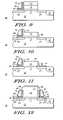
- FIG. 9is a cross-sectional view of a nonvolatile memory device according to another embodiment of the present disclosure after the structure in FIG. 5 has undergone a patterning and etching of one bitcell control gate;
- FIG. 10is a cross-sectional view of a nonvolatile memory device after the processes of FIG. 9 , and after the device has had nitride sidewall spacers and nitride spacers formed;
- FIG. 11is a cross-sectional view of a nonvolatile memory device after the processes of FIG. 10 and after the control gate and the select gate have been silicided;
- FIG. 12is a cross-sectional view of a nonvolatile memory device according to another embodiment of the present disclosure after the processes of FIG. 4 showing silicided control and select gates for a 2-bit storage cell;
- FIG. 13is a cross-sectional view of a nonvolatile memory device according to another embodiment of the present disclosure after the processes of FIG. 4 and after the polysilicon has been polished to form a control gate;
- FIG. 14is a cross-sectional view of the nonvolatile memory device of FIG. 13 after formation of the select gate and silicidation of both control gate and select gates;
- FIG. 15is a cross-sectional view of a nonvolatile memory device according to another embodiment of the present disclosure whereby the nanoclusters are deposited prior to forming the first polysilicon layer;
- FIG. 16is a cross-sectional view of the non-volatile memory device from FIG. 15 after the layers have been patterned and etched;
- FIG. 17is a cross-sectional view of the non-volatile memory device from FIG. 16 after formation of oxide sidewall spacers and deposition of a second polysilicon layer;
- FIG. 18is a cross-sectional view of the non-volatile memory device from FIG. 17 after the control gates and the select gates have been patterned and etched;
- FIG. 19is a cross-sectional view of the non-volatile memory device from FIG. 18 after formation of nitride sidewall spacers and nitride spacers for the select gates and control gates;
- FIG. 20is a cross-sectional view of the non-volatile memory device from FIG. 19 after silicidation of the select gates and control gates;
- FIG. 21is a cross-sectional view of a non-volatile memory device according to another embodiment of the present disclosure showing a contact to multiple silicided control gates.
- FIGS. 1-8show cross-sectional views of a semiconductor device during the various stages of manufacture of a memory device including nanoclusters and silicided select gates and control gates according to a first embodiment of the present invention.
- FIG. 1is a cross-sectional view of a nonvolatile memory (NVM) device 10 according to one embodiment of the present disclosure.
- Memory device 10includes a substrate 12 that contains bitcell wells of a first conductivity type that may overlie a deep well of a second conductivity type, opposite the first conductivity type.
- the first conductivity typeincludes p-type and the second conductivity type includes n-type dopant. These are not shown for clarity but are known to those of skill in the art.
- Memory devicealso includes an isolation structure 13 such as shallow trench isolation. Other isolation structures such as LOCOS are also contemplated.
- FIG. 2shows the memory device 10 after the gate oxide layer 17 has been formed.
- this oxideis on the order of approximately 20-50 ⁇ and has been thermally grown.
- Layer 17can also be formed by other methods including chemical vapor deposition and can also be formed from another dielectric such as silicon oxynitride, hafnium oxide, aluminum oxide, or the like.
- a first layer of polysilicon 19is then formed over oxide layer 17 .
- Polysilicon layer 19will serve as the conductive layer for the select gate portion of the NVM device.
- polysilicon layer 19is approximately 1000 ⁇ thick and includes an n-type dopant.
- Nitride layer 21is deposited over polysilicon layer 19 .
- Nitride layer 21may be used as an etch stop layer for subsequent processing steps as discussed later.
- layer 21may include silicon nitride, silicon oxynitride, silicon rich oxynitride, or the like.
- Nitride layer 21is approximately 700-1000 ⁇ or thicker and is formed by conventional processes including chemical vapor deposition (CVD).
- FIG. 3is a cross-sectional view of the NVM device after polysilicon layer 19 has been patterned and etched using conventional lithographic and etch methods. At this time, the well doping under the area that will become the control gate can be differentiated from the well doping under the select gate with a well implant layer 23 .
- This additional well implantcan be n-type or p-type, depending on the relative values of the control and select gate threshold voltages.
- FIG. 4is a cross-sectional view of the memory device after formation of a layer of oxide 25 .
- the oxide layer 25is formed to a thickness of approximately 50-70 ⁇ and is thermally grown.
- Oxide layer 25can also be another dielectric material such as silicon oxynitride or a high dielectric constant (high K) and may be formed by other methods including CVD, atomic layer deposition (ALD), or the like.
- Nanoclusters 29can be formed by CVD, by aerosol deposition techniques, by spin on coating techniques, by self assembly techniques such as e.g. annealing a thin film to form the nanoclusters, or the like.
- Typical nanoclustersinclude Si, SiGe, Al, Au, a silicon and germanium alloy, or other types of conductive material or doped or undoped semiconductive material.
- the nanoclustersare formed at the preferred densities in the range of 5 ⁇ 10 11 cm ⁇ 2 to 1.0 ⁇ 10 12 cm ⁇ 2 and a diameter of 50-150 ⁇ or larger and with a coverage of approximately 25%.
- a layer of dielectric 27may then be deposited to serve as the dielectric separating the previously deposited nanoclusters 29 from the control gate.
- Dielectric layer 27is typically SiO 2 and may be deposited to a thickness of 80-120 ⁇ .
- Dielectric layer 27can also be a layer of higher permittivity such as aluminum oxide.
- a second layer of polysilicon 31is formed over dielectric 27 .
- Polysilicon 31will serve as the conductive layer for the control gate portion of the NVM device.
- polysilicon layer 31is approximately 1500 ⁇ thick and may include a p-type dopant. The thickness of polysilicon layer 31 will be dependent on the required length of the control gate so may be either less than or greater than 1500 ⁇ thick.
- FIG. 5a cross sectional view of the memory device is shown after etch processes have been performed to form the control gate 33 in a sidewall spacer configuration.
- etch processeshave been performed to form the control gate 33 in a sidewall spacer configuration.
- an anisotropic dry etchis used.
- a further processmay then be used to remove the nanoclusters and oxide from the top surface of nitride layer 21 while retaining the nanoclusters and oxide that separate the control gate portion of the device from the select gate portion of the device. This may be done by a dry etch or a combination of dry and wet etch processes and can also remove nitride layer 21 .
- Select gate 37is comprised of both polysilicon layer 19 as well as oxide layer 17 .
- Nitride layer 21is now nitride layers 39 over the separate select gate regions 37 .
- nitride layers 39are then removed. This may be performed using an isotropic wet etch in hot phosphoric acid without using a mask.
- source and drain extensionsmay be formed by well know implantation techniques. The extensions may be doped n-type.
- a layer of nitride or like materialis then formed over the entire structure.
- the nitridemay be formed by CVD or like processes and, according to one embodiment, be approximately 700 ⁇ thick.
- a conventional anisotropic nitride etch processmay then be used to form sidewall spacers 41 adjacent the control gates 33 , sidewall spacers 42 separating the select gates 37 , and sidewall spacers 43 that will further serve to separate oxide layer 25 from any further materials formed overlying select gates 37 .
- Sidewall spacers 41 , 42 , and 43are shown in FIG. 7 .
- FIG. 8is a cross sectional view of the resulting structure in accordance with the first embodiment of the present invention.
- the structure of FIG. 7has been processed to form select gate silicide 47 , control gate silicide 45 , and silicided source and drain areas 24 .
- a layer of metalsuch as titanium, tungsten, cobalt, nickel, an alloy or other like material is blanket deposited.
- An annealreacts the metal with any exposed silicon to form a silicide. Any unreacted metal is subsequently removed. A final anneal can then be performed.
- the resultis a memory device with silicided control gates and select gates whereby the silicided areas are electrically isolated from one another by dielectric materials. Sidewall spacers 41 , 42 , and 43 are silicide resistant areas and will, therefore, remain essentially unchanged.
- the masking layer used to define select gate 37is shaped such that the subsequent sidewall spacer control gates, 33 , are contiguous and provide sufficient area to permit a lithographically defined contact to be patterned. This is more easily seen in FIG. 21 whereby a single contact 100 is seen to contact the control gates 33 prepared in the sidewall spacer method of the aforementioned embodiment.
- FIGS. 9-11show cross-sectional views of a semiconductor device during the various stages of manufacture of a memory device including nanoclusters and a silicided select gate and control gate according to a second embodiment of the present invention.
- FIG. 9a structure is shown after the structure of FIG. 5 has been patterned and etched according to a preferred embodiment resulting in a single bitcell device with control gate 33 .
- Conventional masking techniquesare used subsequent to the formation of the spacer control gate to form the single bitcell.
- a conventional dry etch process, a wet etch or a combination of bothmay be used to attain the structure shown in FIG. 9 .
- Nitride layer 21may then be removed using a masked or unmasked isotropic wet etch in hot phosphoric acid, or an anisotropic dry etch with conventional masking techniques.
- a layer of nitride or like materialis then formed over the entire structure.
- the nitridemay be formed by CVD or like processes and, according to one embodiment, be approximately 700 ⁇ thick.
- a conventional anisotropic nitride etch processmay then be used to form sidewall spacer 42 and sidewall spacer 43 that will further serve to separate oxide layer 25 from any further materials formed overlying select gate 37 as shown in cross section in FIG. 10 .
- FIG. 11is a cross sectional view of the resulting structure in accordance with the second embodiment of the present invention.
- the structure of FIG. 10has been further processed to form select gate silicide 47 , control gate silicide 45 , and silicided source and drain areas 24 .
- FIG. 12is a cross section of a third embodiment of the present invention showing a 2-bit memory cell.
- the structure of FIG. 4has been etched in a manner similar to that described for FIG. 5 .
- the process step that removes the nanoclusters 29 , oxide 25 , and control gate 33is performed in a manner that recesses control gates 33 below select gate 37 .
- the select gate 37has been masked to allow for the anisotropic etch of control gates 33 as well as nanoclusters 29 and oxide 25 .
- a combination of anisotropic etch with isotropic etchmay also be performed.
- the subsequent formation of a blanket nitride layeris followed by an anisotropic etch.
- sidewall spacers 44 and 41This results in sidewall spacers 44 and 41 .
- sidewall spacers 44overlie the nanoclusters 29 and oxide layer 25 while sidewall spacers 41 overlie control gates 33 .
- spacers 41overly only a small portion of control gate 33 .
- Further processingis performed whereby a layer of metal such as titanium, tungsten, cobalt, nickel, an alloy or other like material is blanket deposited. An anneal reacts the metal with any exposed silicon to form a silicide. Any unreacted metal is subsequently removed. A final anneal can then be performed. The result is a memory device with silicided control gates that are recessed with respect to silicided select gates.
- a single bit memory cellcould also be formed in the manner described in FIG. 12 for the 2-bit memory cell.
- the result of processingwould be a single spacer on one side of the select gate as opposed to the double spacer as shown in FIG. 12 .
- FIGS. 13 and 14are cross sectional views of a memory device according to a fourth embodiment of the present invention.
- a polish processsuch as chemical mechanical polishing (CMP) is used to planarize the second layer of polysilicon 31 as well as remove nanoclusters 29 and oxide 27 overlying nitride 21 .
- CMPchemical mechanical polishing
- Multiple slurriesmay be used to achieve the best planarity of the structure. Polishing is stopped when nitride layer 21 is cleared of polysilicon layer 31 .
- a blanket etchback processis also contemplated for the planarization of the second layer of polysilicon 31 .
- FIG. 14shows a cross sectional view of a memory device according to the fourth embodiment of the present invention.
- Lithographic and etch processesdefine control gates 33 and select gates 37 .
- An anisotropic polysilicon etchis preferred.
- the processes as described for the first embodiment and shown in FIGS. 6-8may be performed.
- the resulting structureis an essentially planar silicided control gate 33 with recessed and silicided select gates 37 .
- FIGS. 15-20are cross sectional views of a memory device according to a fifth embodiment of the present invention.
- a gate oxide layer 17is formed overlying a substrate 12 .
- oxide layer 17is on the order of approximately 50-70 ⁇ and has been thermally grown.
- Layer 17can also be formed by other methods including chemical vapor deposition and can also be formed from another dielectric such as silicon oxynitride, hafnium oxide, aluminum oxide, or the like.
- Nanoclusters 29are then formed by island growth during CVD, by aerosol deposition techniques, by spin on coating techniques, by self assembly techniques such as e.g. annealing a thin film to form the nanoclusters, or the like.
- Typical nanoclustersinclude Si, SiGe, Al, Au, a silicon and germanium alloy, or other types of conductive material or doped or undoped semiconductive material.
- the nanoclustersare formed at the preferred densities in the range of 5 ⁇ 10 11 cm ⁇ 2 to 1.1 ⁇ 10 12 cm ⁇ 2 and an undoped diameter of 50-150 ⁇ or larger and with a coverage of approximately 25% or less.
- a layer of dielectric 27is then deposited which will serve as the oxide separating the subsequently deposited nanoclusters 29 from the control gate.
- Dielectric layer 27is typically SiO 2 and is deposited to a thickness of 80-120 ⁇ .
- a first layer of polysilicon 19is formed over nanoclusters 29 .
- Polysilicon 19will serve as the conductive layer for the control gate portion of the NVM device.
- polysilicon layer 19is approximately 1500 ⁇ thick.
- An oxide layeris formed overlying polysilicon layer 19 .
- Oxide layer 49may be deposited by CVD or may be thermally grown.
- a preferred thicknessis approximately 700-1000 ⁇ .
- a nitride layer 21is formed overlying oxide layer 49 .
- Nitride layer 21may be used as an etch stop layer for subsequent processing steps as discussed later.
- layer 21may include silicon nitride, silicon oxynitride, silicon rich oxynitride, or the like.
- Nitride layer 21is approximately 700-1000 ⁇ or thicker and is formed by conventional processes including CVD.
- FIG. 16lithographic and etch processes have been performed resulting in a patterned first gate structure. This structure may go on to form the control gate for the memory device.
- FIG. 17is a cross sectional view after further processing on the structure from FIG. 16 .
- a layer of oxide, 51is deposited using a CVD or similar technique.
- a subsequent anisotropic etchis used to form oxide sidewall spacers on control gate polysilicon structure, 19 .
- a layer of oxide 53is formed by either a thermal growth, by CVD or the like.
- a preferred thicknessis 20-50 ⁇ .
- Layer 53can also be formed by other methods well known in the art for formation of oxides
- Layer 53can also be formed from another dielectric such as silicon oxynitride, hafnium oxide, aluminum oxide, or the like.
- a second layer of polysilicon 55is then formed. Polysilicon 55 will serve as the conductive layer for the select gate portion of the NVM device.
- polysilicon layer 55is approximately 1500 ⁇ thick and may include a p-type dopant.
- a polish process, such as CMP,is then used to planarize the structure.
- Polysilicon layer 55is then patterned and etched to form select gates 55 .
- An anti-reflective coating (ARC)may be formed over the entire structure at this time to facilitate fine mask patterning.
- ARCanti-reflective coating
- nitride layer 49 , oxide layer 21 , polysilicon layer 19 , nanoclusters 29 , and oxide layer 17are simultaneously patterned and etched to define what will become the control gate portion of the memory device.
- a patterning and etching process for the control gate portion of the memory device occurring subsequent to the definition of the select gateis also contemplated. The resulting cross sectional view is shown in FIG. 18 .
- FIG. 19is a cross sectional view of the memory device after further processing has occurred.
- Nitride layer 21has been removed, preferably by using an isotropic wet etch in hot phosphoric acid or an anisotropic dry etch.
- Oxide layer 49is also removed and may be removed in a similar manner as nitride layer 21 .
- the resulting structureis one in which the control gate portion of the memory device is recessed with respect to the select gate portion of the memory device.
- a blanket nitride layeris then formed which is then anisotropically etched to form sidewalls 59 and 61 for the control gate, as well as sidewalls 57 for the select gates.
- source and drain areas 23may be formed by ion implantation or other techniques.
- FIG. 20is a cross sectional view of the memory device after processing has been done to form silicided select gates 47 , silicided control gates 45 , and silicided source and drain areas 24 .
- a process as described previouslymay be done to accomplish the silicidation.
- the memory device after formation of a contact plugis shown in cross section in FIG. 21 .
- the cross sectional viewis based on the method provided to form the silicided sidewall spacer control gates 33 and recessed silicided select gates 37 from FIG. 8 .
- a dielectric layeris first formed overlying the structure as shown in FIG. 20 .
- the dielectricmay be SiO 2 , BPSG, PSG, a spin-on dielectric or the like. Planarization of the dielectric may be performed prior to the lithographic and etch processes. A conventional process is used to define a contact hole in the dielectric which will contact the underlying silicide of the control gate. Metallization of the contact is then done.
- Thismay include a barrier deposition and a CVD tungsten fill, followed by a CMP process to remove the overburden of tungsten.
- a selective tungsten processis also contemplated as is other metallization techniques known in the art. As noted previously, careful selection of the patterning of the control gates 33 will enable the contact to the control gates 33 as shown.
- a 2-bitcell memory deviceincludes a split gate device that uses nanoclusters for charge storage in which both the select gates and the control gates have been silicided and whereby the select gates are recessed with respect to the control gates.
- the silicides for the control gates and select gatesare separated from one another by at least a spacer material that overlies the conductive portion of the select gate.
- the nanoclustersare underlying the control gate portion of the memory device.
- a single bitcell memory devicethat uses nanoclusters for charge storage in which both the select gate and the control gate have been silicided and whereby the select gate is recessed with respect to the control gate is shown.
- the silicides for the control gate and select gateare separated from one another by at least a spacer material that overlies the conductive portion of the select gate.
- the nanoclustersare underlying the control gate portion of the memory device.
- a 2-bit storage cellthat uses nanoclusters for charge storage in which both the select gate and the control gates have been silicided is shown.
- the control gatesare recessed with respect to the select gate.
- the silicides for the control gates and select gateare separated from one another by at least a spacer material that overlies the nanoclusters.
- the nanoclustersare underlying the control gate portion of the memory device.
- a polish processis used to planarize a conductive layer for the control gates and select gates. Further processing recesses the select gates with respect to the control gates. Both select gates and control gates are silicided. At least a spacer material separates the silicide of the select gate from the silicide for the control gate. The nanoclusters are underlying the control gate portion of the memory device.
- a polish processis used to planarize a conductive layer for the selective gate portion of the memory device.
- the nanoclustersare formed underlying the control gate portion of the memory device.
- both select gates and control gatesare silicided and are separated from one another by at least a spacer material.
- the control gatesare recessed with respect to the select gate portions.
Landscapes
- Engineering & Computer Science (AREA)
- Chemical & Material Sciences (AREA)
- Nanotechnology (AREA)
- Physics & Mathematics (AREA)
- Mathematical Physics (AREA)
- Crystallography & Structural Chemistry (AREA)
- Theoretical Computer Science (AREA)
- Condensed Matter Physics & Semiconductors (AREA)
- Microelectronics & Electronic Packaging (AREA)
- Power Engineering (AREA)
- Computer Hardware Design (AREA)
- Manufacturing & Machinery (AREA)
- General Physics & Mathematics (AREA)
- Chemical Kinetics & Catalysis (AREA)
- Semiconductor Memories (AREA)
- Non-Volatile Memory (AREA)
Abstract
Description
Claims (11)
Priority Applications (5)
| Application Number | Priority Date | Filing Date | Title |
|---|---|---|---|
| US11/376,410US7700439B2 (en) | 2006-03-15 | 2006-03-15 | Silicided nonvolatile memory and method of making same |
| KR1020087022525AKR101320859B1 (en) | 2006-03-15 | 2007-02-22 | Silicided nonvolatile memory and method of making same |
| PCT/US2007/062540WO2007106647A2 (en) | 2006-03-15 | 2007-02-22 | Silicided nonvolatile memory and method of making same |
| CN2007800088858ACN101401200B (en) | 2006-03-15 | 2007-02-22 | Siliconized nonvolatile memory and method of manufacturing the same |
| TW096107714ATWI429026B (en) | 2006-03-15 | 2007-03-06 | Deuterated non-volatile memory and manufacturing method thereof |
Applications Claiming Priority (1)
| Application Number | Priority Date | Filing Date | Title |
|---|---|---|---|
| US11/376,410US7700439B2 (en) | 2006-03-15 | 2006-03-15 | Silicided nonvolatile memory and method of making same |
Publications (2)
| Publication Number | Publication Date |
|---|---|
| US20070218633A1 US20070218633A1 (en) | 2007-09-20 |
| US7700439B2true US7700439B2 (en) | 2010-04-20 |
Family
ID=38510135
Family Applications (1)
| Application Number | Title | Priority Date | Filing Date |
|---|---|---|---|
| US11/376,410Active2026-06-09US7700439B2 (en) | 2006-03-15 | 2006-03-15 | Silicided nonvolatile memory and method of making same |
Country Status (5)
| Country | Link |
|---|---|
| US (1) | US7700439B2 (en) |
| KR (1) | KR101320859B1 (en) |
| CN (1) | CN101401200B (en) |
| TW (1) | TWI429026B (en) |
| WO (1) | WO2007106647A2 (en) |
Cited By (6)
| Publication number | Priority date | Publication date | Assignee | Title |
|---|---|---|---|---|
| US20090108325A1 (en)* | 2007-10-29 | 2009-04-30 | Kang Sung-Taeg | Split gate device and method for forming |
| US20090111229A1 (en)* | 2007-10-31 | 2009-04-30 | Steimle Robert F | Method of forming a split gate non-volatile memory cell |
| US20100248466A1 (en)* | 2009-03-31 | 2010-09-30 | Loiko Konstantin V | Method for making a stressed non-volatile memory device |
| US20140050029A1 (en)* | 2012-08-20 | 2014-02-20 | Sung-taeg Kang | Split-gate memory cells having select-gate sidewall metal silicide regions and related manufacturing methods |
| US20140357072A1 (en)* | 2013-05-31 | 2014-12-04 | Jinmiao J. Shen | Methods and structures for split gate memory |
| US20150200279A1 (en)* | 2014-01-12 | 2015-07-16 | United Microelectronics Corp. | Method of manufacturing memory cell |
Families Citing this family (30)
| Publication number | Priority date | Publication date | Assignee | Title |
|---|---|---|---|---|
| US7495280B2 (en) | 2006-05-16 | 2009-02-24 | Taiwan Semiconductor Manufacturing Company, Ltd. | MOS devices with corner spacers |
| US7579243B2 (en)* | 2006-09-26 | 2009-08-25 | Freescale Semiconductor, Inc. | Split gate memory cell method |
| US7482270B2 (en)* | 2006-12-05 | 2009-01-27 | International Business Machines Corporation | Fully and uniformly silicided gate structure and method for forming same |
| US7943452B2 (en) | 2006-12-12 | 2011-05-17 | International Business Machines Corporation | Gate conductor structure |
| US7416945B1 (en)* | 2007-02-19 | 2008-08-26 | Freescale Semiconductor, Inc. | Method for forming a split gate memory device |
| US8110465B2 (en)* | 2007-07-30 | 2012-02-07 | International Business Machines Corporation | Field effect transistor having an asymmetric gate electrode |
| US7745344B2 (en)* | 2007-10-29 | 2010-06-29 | Freescale Semiconductor, Inc. | Method for integrating NVM circuitry with logic circuitry |
| US7795091B2 (en)* | 2008-04-30 | 2010-09-14 | Winstead Brian A | Method of forming a split gate memory device and apparatus |
| US7955964B2 (en) | 2008-05-14 | 2011-06-07 | Taiwan Semiconductor Manufacturing Company, Ltd. | Dishing-free gap-filling with multiple CMPs |
| US8048752B2 (en) | 2008-07-24 | 2011-11-01 | Taiwan Semiconductor Manufacturing Company, Ltd. | Spacer shape engineering for void-free gap-filling process |
| US8173505B2 (en)* | 2008-10-20 | 2012-05-08 | Freescale Semiconductor, Inc. | Method of making a split gate memory cell |
| WO2010082328A1 (en)* | 2009-01-15 | 2010-07-22 | ルネサスエレクトロニクス株式会社 | Semiconductor device, and method for manufacturing the same |
| US8263463B2 (en)* | 2009-03-30 | 2012-09-11 | Freescale Semiconductor, Inc. | Nonvolatile split gate memory cell having oxide growth |
| US8372699B2 (en)* | 2010-02-22 | 2013-02-12 | Freescale Semiconductor, Inc. | Method for forming a split-gate memory cell |
| US9209197B2 (en)* | 2012-12-14 | 2015-12-08 | Cypress Semiconductor Corporation | Memory gate landing pad made from dummy features |
| US9966477B2 (en) | 2012-12-14 | 2018-05-08 | Cypress Semiconductor Corporation | Charge trapping split gate device and method of fabricating same |
| US20140167142A1 (en)* | 2012-12-14 | 2014-06-19 | Spansion Llc | Use Disposable Gate Cap to Form Transistors, and Split Gate Charge Trapping Memory Cells |
| US8884358B2 (en)* | 2013-01-24 | 2014-11-11 | Freescale Semiconductor, Inc. | Method of making a non-volatile memory (NVM) cell structure |
| US9111866B2 (en)* | 2013-03-07 | 2015-08-18 | Globalfoundries Singapore Pte. Ltd. | Method of forming split-gate cell for non-volative memory devices |
| US9590058B2 (en) | 2013-06-28 | 2017-03-07 | Nxp Usa, Inc. | Methods and structures for a split gate memory cell structure |
| JP2015185613A (en)* | 2014-03-20 | 2015-10-22 | ルネサスエレクトロニクス株式会社 | Semiconductor device and manufacturing method thereof |
| CN104952875B (en)* | 2014-03-27 | 2019-07-09 | 联华电子股份有限公司 | Memory cell and manufacturing method thereof |
| US9257445B2 (en)* | 2014-05-30 | 2016-02-09 | Freescale Semiconductor, Inc. | Method of making a split gate non-volatile memory (NVM) cell and a logic transistor |
| US9691883B2 (en)* | 2014-06-19 | 2017-06-27 | Taiwan Semiconductor Manufacturing Co., Ltd. | Asymmetric formation approach for a floating gate of a split gate flash memory structure |
| US9728410B2 (en)* | 2014-10-07 | 2017-08-08 | Nxp Usa, Inc. | Split-gate non-volatile memory (NVM) cell and method therefor |
| US9741868B2 (en)* | 2015-04-16 | 2017-08-22 | Taiwan Semiconductor Manufacturing Co., Ltd. | Self-aligned split gate flash memory |
| CN106684085B (en)* | 2015-11-11 | 2021-02-02 | 联华电子股份有限公司 | Semiconductor device and method of making the same |
| JP2017139336A (en)* | 2016-02-03 | 2017-08-10 | 渡辺 浩志 | Structure of flash memory and operation method of them |
| US10879181B2 (en)* | 2016-11-28 | 2020-12-29 | Taiwan Semiconductor Manufacturing Co., Ltd. | Embedded non-volatile memory with side word line |
| US10903326B2 (en) | 2019-01-13 | 2021-01-26 | United Microelectronics Corp. | Semiconductor device and method for fabricating the same |
Citations (10)
| Publication number | Priority date | Publication date | Assignee | Title |
|---|---|---|---|---|
| US5408115A (en) | 1994-04-04 | 1995-04-18 | Motorola Inc. | Self-aligned, split-gate EEPROM device |
| US5824584A (en) | 1997-06-16 | 1998-10-20 | Motorola, Inc. | Method of making and accessing split gate memory device |
| US5969383A (en) | 1997-06-16 | 1999-10-19 | Motorola, Inc. | Split-gate memory device and method for accessing the same |
| US6816414B1 (en) | 2003-07-31 | 2004-11-09 | Freescale Semiconductor, Inc. | Nonvolatile memory and method of making same |
| US20050176202A1 (en) | 2004-02-10 | 2005-08-11 | Renesas Technology Corp. | Nonvolatile semiconductor memory and making method thereof |
| US20050180210A1 (en) | 2001-10-31 | 2005-08-18 | Eliyahou Harari | Multi-state non-volatile integrated circuit memory systems that employ dielectric storage elements |
| US6964902B2 (en) | 2004-02-26 | 2005-11-15 | Freescale Semiconductor, Inc. | Method for removing nanoclusters from selected regions |
| US20060017094A1 (en) | 2004-07-22 | 2006-01-26 | Kwang-Bok Kim | Non-volatile memory devices with improved insulation layers and methods of manufacturing such devices |
| US20060203543A1 (en)* | 2005-03-08 | 2006-09-14 | Magnachip Semiconductor Ltd. | Non-volatile memory device and method for fabricating the same |
| US7456465B2 (en) | 2005-09-30 | 2008-11-25 | Freescale Semiconductor, Inc. | Split gate memory cell and method therefor |
Family Cites Families (2)
| Publication number | Priority date | Publication date | Assignee | Title |
|---|---|---|---|---|
| US6194272B1 (en)* | 1998-05-19 | 2001-02-27 | Mosel Vitelic, Inc. | Split gate flash cell with extremely small cell size |
| CN100565882C (en)* | 2000-03-08 | 2009-12-02 | Nxp股份有限公司 | Method, semi-conductor device manufacturing method |
- 2006
- 2006-03-15USUS11/376,410patent/US7700439B2/enactiveActive
- 2007
- 2007-02-22WOPCT/US2007/062540patent/WO2007106647A2/enactiveApplication Filing
- 2007-02-22KRKR1020087022525Apatent/KR101320859B1/ennot_activeExpired - Fee Related
- 2007-02-22CNCN2007800088858Apatent/CN101401200B/ennot_activeExpired - Fee Related
- 2007-03-06TWTW096107714Apatent/TWI429026B/ennot_activeIP Right Cessation
Patent Citations (10)
| Publication number | Priority date | Publication date | Assignee | Title |
|---|---|---|---|---|
| US5408115A (en) | 1994-04-04 | 1995-04-18 | Motorola Inc. | Self-aligned, split-gate EEPROM device |
| US5824584A (en) | 1997-06-16 | 1998-10-20 | Motorola, Inc. | Method of making and accessing split gate memory device |
| US5969383A (en) | 1997-06-16 | 1999-10-19 | Motorola, Inc. | Split-gate memory device and method for accessing the same |
| US20050180210A1 (en) | 2001-10-31 | 2005-08-18 | Eliyahou Harari | Multi-state non-volatile integrated circuit memory systems that employ dielectric storage elements |
| US6816414B1 (en) | 2003-07-31 | 2004-11-09 | Freescale Semiconductor, Inc. | Nonvolatile memory and method of making same |
| US20050176202A1 (en) | 2004-02-10 | 2005-08-11 | Renesas Technology Corp. | Nonvolatile semiconductor memory and making method thereof |
| US6964902B2 (en) | 2004-02-26 | 2005-11-15 | Freescale Semiconductor, Inc. | Method for removing nanoclusters from selected regions |
| US20060017094A1 (en) | 2004-07-22 | 2006-01-26 | Kwang-Bok Kim | Non-volatile memory devices with improved insulation layers and methods of manufacturing such devices |
| US20060203543A1 (en)* | 2005-03-08 | 2006-09-14 | Magnachip Semiconductor Ltd. | Non-volatile memory device and method for fabricating the same |
| US7456465B2 (en) | 2005-09-30 | 2008-11-25 | Freescale Semiconductor, Inc. | Split gate memory cell and method therefor |
Non-Patent Citations (1)
| Title |
|---|
| International Search Report and Written Opinion. |
Cited By (10)
| Publication number | Priority date | Publication date | Assignee | Title |
|---|---|---|---|---|
| US20090108325A1 (en)* | 2007-10-29 | 2009-04-30 | Kang Sung-Taeg | Split gate device and method for forming |
| US8178406B2 (en)* | 2007-10-29 | 2012-05-15 | Freescale Semiconductor, Inc. | Split gate device and method for forming |
| US20090111229A1 (en)* | 2007-10-31 | 2009-04-30 | Steimle Robert F | Method of forming a split gate non-volatile memory cell |
| US7838363B2 (en) | 2007-10-31 | 2010-11-23 | Freescale Semiconductor, Inc. | Method of forming a split gate non-volatile memory cell |
| US20100248466A1 (en)* | 2009-03-31 | 2010-09-30 | Loiko Konstantin V | Method for making a stressed non-volatile memory device |
| US7960267B2 (en)* | 2009-03-31 | 2011-06-14 | Freescale Semiconductor, Inc. | Method for making a stressed non-volatile memory device |
| US20140050029A1 (en)* | 2012-08-20 | 2014-02-20 | Sung-taeg Kang | Split-gate memory cells having select-gate sidewall metal silicide regions and related manufacturing methods |
| US9165652B2 (en)* | 2012-08-20 | 2015-10-20 | Freescale Semiconductor, Inc. | Split-gate memory cells having select-gate sidewall metal silicide regions and related manufacturing methods |
| US20140357072A1 (en)* | 2013-05-31 | 2014-12-04 | Jinmiao J. Shen | Methods and structures for split gate memory |
| US20150200279A1 (en)* | 2014-01-12 | 2015-07-16 | United Microelectronics Corp. | Method of manufacturing memory cell |
Also Published As
| Publication number | Publication date |
|---|---|
| KR101320859B1 (en) | 2013-10-23 |
| CN101401200B (en) | 2011-07-06 |
| TWI429026B (en) | 2014-03-01 |
| WO2007106647A2 (en) | 2007-09-20 |
| CN101401200A (en) | 2009-04-01 |
| KR20080114735A (en) | 2008-12-31 |
| US20070218633A1 (en) | 2007-09-20 |
| TW200741979A (en) | 2007-11-01 |
| WO2007106647A3 (en) | 2007-12-21 |
Similar Documents
| Publication | Publication Date | Title |
|---|---|---|
| US7700439B2 (en) | Silicided nonvolatile memory and method of making same | |
| KR100805868B1 (en) | Semiconductor device and manufacturing method thereof | |
| US7067379B2 (en) | Silicide gate transistors and method of manufacture | |
| US6091076A (en) | Quantum WELL MOS transistor and methods for making same | |
| JP7160849B2 (en) | Method for forming high voltage transistors with thin gate poly | |
| US7195969B2 (en) | Strained channel CMOS device with fully silicided gate electrode | |
| US6943071B2 (en) | Integrated memory cell and method of fabrication | |
| US7442609B2 (en) | Method of manufacturing a transistor and a method of forming a memory device with isolation trenches | |
| US7211858B2 (en) | Split gate storage device including a horizontal first gate and a vertical second gate in a trench | |
| US7763513B2 (en) | Integrated circuit device and method of manufacture | |
| US9082650B2 (en) | Integrated split gate non-volatile memory cell and logic structure | |
| KR100474150B1 (en) | Fully encapsulated damascene gates for gigabit drams | |
| US6335248B1 (en) | Dual workfunction MOSFETs with borderless diffusion contacts for high-performance embedded DRAM technology | |
| JP2006041276A (en) | Semiconductor device and manufacturing method thereof | |
| JPH1174508A (en) | Semiconductor device and manufacturing method thereof | |
| CN101765915A (en) | Planar double gate transistor storage cell | |
| US20090072293A1 (en) | Flash Memory and Method for Manufacturing the Same | |
| US20070077715A1 (en) | Semiconductor device and method of fabricating the same | |
| US6576949B1 (en) | Integrated circuit having optimized gate coupling capacitance | |
| US20080023756A1 (en) | Semiconductor device and fabricating method thereof | |
| JP2005039280A (en) | Low power flash memory cell and method | |
| US9252246B2 (en) | Integrated split gate non-volatile memory cell and logic device | |
| US6492227B1 (en) | Method for fabricating flash memory device using dual damascene process | |
| US8836019B2 (en) | Recessed channel transistors, and semiconductor devices including a recessed channel transistor | |
| JP2005252280A (en) | Semiconductor device and manufacturing method thereof |
Legal Events
| Date | Code | Title | Description |
|---|---|---|---|
| AS | Assignment | Owner name:FREESCALE SEMICONDUCTOR, INC., TEXAS Free format text:ASSIGNMENT OF ASSIGNORS INTEREST;ASSIGNORS:PRINZ, ERWIN J.;CHANG, KO-MIN;STEIMLE, ROBERT F.;REEL/FRAME:017667/0193;SIGNING DATES FROM 20060313 TO 20060314 Owner name:FREESCALE SEMICONDUCTOR, INC.,TEXAS Free format text:ASSIGNMENT OF ASSIGNORS INTEREST;ASSIGNORS:PRINZ, ERWIN J.;CHANG, KO-MIN;STEIMLE, ROBERT F.;SIGNING DATES FROM 20060313 TO 20060314;REEL/FRAME:017667/0193 | |
| AS | Assignment | Owner name:CITIBANK, N.A. AS COLLATERAL AGENT, NEW YORK Free format text:SECURITY AGREEMENT;ASSIGNORS:FREESCALE SEMICONDUCTOR, INC.;FREESCALE ACQUISITION CORPORATION;FREESCALE ACQUISITION HOLDINGS CORP.;AND OTHERS;REEL/FRAME:018855/0129 Effective date:20061201 Owner name:CITIBANK, N.A. AS COLLATERAL AGENT,NEW YORK Free format text:SECURITY AGREEMENT;ASSIGNORS:FREESCALE SEMICONDUCTOR, INC.;FREESCALE ACQUISITION CORPORATION;FREESCALE ACQUISITION HOLDINGS CORP.;AND OTHERS;REEL/FRAME:018855/0129 Effective date:20061201 | |
| AS | Assignment | Owner name:CITIBANK, N.A.,NEW YORK Free format text:SECURITY AGREEMENT;ASSIGNOR:FREESCALE SEMICONDUCTOR, INC.;REEL/FRAME:024085/0001 Effective date:20100219 Owner name:CITIBANK, N.A., NEW YORK Free format text:SECURITY AGREEMENT;ASSIGNOR:FREESCALE SEMICONDUCTOR, INC.;REEL/FRAME:024085/0001 Effective date:20100219 | |
| STCF | Information on status: patent grant | Free format text:PATENTED CASE | |
| AS | Assignment | Owner name:CITIBANK, N.A., AS COLLATERAL AGENT,NEW YORK Free format text:SECURITY AGREEMENT;ASSIGNOR:FREESCALE SEMICONDUCTOR, INC.;REEL/FRAME:024397/0001 Effective date:20100413 Owner name:CITIBANK, N.A., AS COLLATERAL AGENT, NEW YORK Free format text:SECURITY AGREEMENT;ASSIGNOR:FREESCALE SEMICONDUCTOR, INC.;REEL/FRAME:024397/0001 Effective date:20100413 | |
| AS | Assignment | Owner name:CITIBANK, N.A., AS NOTES COLLATERAL AGENT, NEW YORK Free format text:SECURITY AGREEMENT;ASSIGNOR:FREESCALE SEMICONDUCTOR, INC.;REEL/FRAME:030633/0424 Effective date:20130521 Owner name:CITIBANK, N.A., AS NOTES COLLATERAL AGENT, NEW YOR Free format text:SECURITY AGREEMENT;ASSIGNOR:FREESCALE SEMICONDUCTOR, INC.;REEL/FRAME:030633/0424 Effective date:20130521 | |
| FPAY | Fee payment | Year of fee payment:4 | |
| AS | Assignment | Owner name:CITIBANK, N.A., AS NOTES COLLATERAL AGENT, NEW YORK Free format text:SECURITY AGREEMENT;ASSIGNOR:FREESCALE SEMICONDUCTOR, INC.;REEL/FRAME:031591/0266 Effective date:20131101 Owner name:CITIBANK, N.A., AS NOTES COLLATERAL AGENT, NEW YOR Free format text:SECURITY AGREEMENT;ASSIGNOR:FREESCALE SEMICONDUCTOR, INC.;REEL/FRAME:031591/0266 Effective date:20131101 | |
| AS | Assignment | Owner name:FREESCALE SEMICONDUCTOR, INC., TEXAS Free format text:PATENT RELEASE;ASSIGNOR:CITIBANK, N.A., AS COLLATERAL AGENT;REEL/FRAME:037354/0225 Effective date:20151207 Owner name:FREESCALE SEMICONDUCTOR, INC., TEXAS Free format text:PATENT RELEASE;ASSIGNOR:CITIBANK, N.A., AS COLLATERAL AGENT;REEL/FRAME:037356/0143 Effective date:20151207 Owner name:FREESCALE SEMICONDUCTOR, INC., TEXAS Free format text:PATENT RELEASE;ASSIGNOR:CITIBANK, N.A., AS COLLATERAL AGENT;REEL/FRAME:037356/0553 Effective date:20151207 | |
| AS | Assignment | Owner name:MORGAN STANLEY SENIOR FUNDING, INC., MARYLAND Free format text:ASSIGNMENT AND ASSUMPTION OF SECURITY INTEREST IN PATENTS;ASSIGNOR:CITIBANK, N.A.;REEL/FRAME:037486/0517 Effective date:20151207 | |
| AS | Assignment | Owner name:MORGAN STANLEY SENIOR FUNDING, INC., MARYLAND Free format text:ASSIGNMENT AND ASSUMPTION OF SECURITY INTEREST IN PATENTS;ASSIGNOR:CITIBANK, N.A.;REEL/FRAME:037518/0292 Effective date:20151207 | |
| AS | Assignment | Owner name:NORTH STAR INNOVATIONS INC., CALIFORNIA Free format text:ASSIGNMENT OF ASSIGNORS INTEREST;ASSIGNOR:FREESCALE SEMICONDUCTOR, INC.;REEL/FRAME:037694/0264 Effective date:20151002 | |
| AS | Assignment | Owner name:NXP, B.V., F/K/A FREESCALE SEMICONDUCTOR, INC., NETHERLANDS Free format text:RELEASE BY SECURED PARTY;ASSIGNOR:MORGAN STANLEY SENIOR FUNDING, INC.;REEL/FRAME:040925/0001 Effective date:20160912 Owner name:NXP, B.V., F/K/A FREESCALE SEMICONDUCTOR, INC., NE Free format text:RELEASE BY SECURED PARTY;ASSIGNOR:MORGAN STANLEY SENIOR FUNDING, INC.;REEL/FRAME:040925/0001 Effective date:20160912 | |
| AS | Assignment | Owner name:NXP B.V., NETHERLANDS Free format text:RELEASE BY SECURED PARTY;ASSIGNOR:MORGAN STANLEY SENIOR FUNDING, INC.;REEL/FRAME:040928/0001 Effective date:20160622 | |
| AS | Assignment | Owner name:MORGAN STANLEY SENIOR FUNDING, INC., MARYLAND Free format text:CORRECTIVE ASSIGNMENT TO CORRECT THE REMOVE PATENTS 8108266 AND 8062324 AND REPLACE THEM WITH 6108266 AND 8060324 PREVIOUSLY RECORDED ON REEL 037518 FRAME 0292. ASSIGNOR(S) HEREBY CONFIRMS THE ASSIGNMENT AND ASSUMPTION OF SECURITY INTEREST IN PATENTS;ASSIGNOR:CITIBANK, N.A.;REEL/FRAME:041703/0536 Effective date:20151207 | |
| MAFP | Maintenance fee payment | Free format text:PAYMENT OF MAINTENANCE FEE, 8TH YEAR, LARGE ENTITY (ORIGINAL EVENT CODE: M1552) Year of fee payment:8 | |
| AS | Assignment | Owner name:SHENZHEN XINGUODU TECHNOLOGY CO., LTD., CHINA Free format text:CORRECTIVE ASSIGNMENT TO CORRECT THE TO CORRECT THE APPLICATION NO. FROM 13,883,290 TO 13,833,290 PREVIOUSLY RECORDED ON REEL 041703 FRAME 0536. ASSIGNOR(S) HEREBY CONFIRMS THE THE ASSIGNMENT AND ASSUMPTION OF SECURITYINTEREST IN PATENTS.;ASSIGNOR:MORGAN STANLEY SENIOR FUNDING, INC.;REEL/FRAME:048734/0001 Effective date:20190217 | |
| AS | Assignment | Owner name:MORGAN STANLEY SENIOR FUNDING, INC., MARYLAND Free format text:CORRECTIVE ASSIGNMENT TO CORRECT THE REMOVE APPLICATION11759915 AND REPLACE IT WITH APPLICATION 11759935 PREVIOUSLY RECORDED ON REEL 037486 FRAME 0517. ASSIGNOR(S) HEREBY CONFIRMS THE ASSIGNMENT AND ASSUMPTION OF SECURITYINTEREST IN PATENTS;ASSIGNOR:CITIBANK, N.A.;REEL/FRAME:053547/0421 Effective date:20151207 | |
| AS | Assignment | Owner name:NXP B.V., NETHERLANDS Free format text:CORRECTIVE ASSIGNMENT TO CORRECT THE REMOVEAPPLICATION 11759915 AND REPLACE IT WITH APPLICATION11759935 PREVIOUSLY RECORDED ON REEL 040928 FRAME 0001. ASSIGNOR(S) HEREBY CONFIRMS THE RELEASE OF SECURITYINTEREST;ASSIGNOR:MORGAN STANLEY SENIOR FUNDING, INC.;REEL/FRAME:052915/0001 Effective date:20160622 | |
| AS | Assignment | Owner name:NXP, B.V. F/K/A FREESCALE SEMICONDUCTOR, INC., NETHERLANDS Free format text:CORRECTIVE ASSIGNMENT TO CORRECT THE REMOVEAPPLICATION 11759915 AND REPLACE IT WITH APPLICATION11759935 PREVIOUSLY RECORDED ON REEL 040925 FRAME 0001. ASSIGNOR(S) HEREBY CONFIRMS THE RELEASE OF SECURITYINTEREST;ASSIGNOR:MORGAN STANLEY SENIOR FUNDING, INC.;REEL/FRAME:052917/0001 Effective date:20160912 | |
| MAFP | Maintenance fee payment | Free format text:PAYMENT OF MAINTENANCE FEE, 12TH YEAR, LARGE ENTITY (ORIGINAL EVENT CODE: M1553); ENTITY STATUS OF PATENT OWNER: LARGE ENTITY Year of fee payment:12 |