US7700157B2 - Method of producing regular arrays of nano-scale objects using nano-structured block-copolymeric materials - Google Patents
Method of producing regular arrays of nano-scale objects using nano-structured block-copolymeric materialsDownload PDFInfo
- Publication number
- US7700157B2 US7700157B2US11/508,514US50851406AUS7700157B2US 7700157 B2US7700157 B2US 7700157B2US 50851406 AUS50851406 AUS 50851406AUS 7700157 B2US7700157 B2US 7700157B2
- Authority
- US
- United States
- Prior art keywords
- method described
- array
- substrate
- catalytic material
- nano
- Prior art date
- Legal status (The legal status is an assumption and is not a legal conclusion. Google has not performed a legal analysis and makes no representation as to the accuracy of the status listed.)
- Expired - Fee Related, expires
Links
Images


Classifications
- B—PERFORMING OPERATIONS; TRANSPORTING
- B81—MICROSTRUCTURAL TECHNOLOGY
- B81C—PROCESSES OR APPARATUS SPECIALLY ADAPTED FOR THE MANUFACTURE OR TREATMENT OF MICROSTRUCTURAL DEVICES OR SYSTEMS
- B81C1/00—Manufacture or treatment of devices or systems in or on a substrate
- B81C1/00015—Manufacture or treatment of devices or systems in or on a substrate for manufacturing microsystems
- B81C1/00023—Manufacture or treatment of devices or systems in or on a substrate for manufacturing microsystems without movable or flexible elements
- B81C1/00031—Regular or irregular arrays of nanoscale structures, e.g. etch mask layer
- B—PERFORMING OPERATIONS; TRANSPORTING
- B82—NANOTECHNOLOGY
- B82Y—SPECIFIC USES OR APPLICATIONS OF NANOSTRUCTURES; MEASUREMENT OR ANALYSIS OF NANOSTRUCTURES; MANUFACTURE OR TREATMENT OF NANOSTRUCTURES
- B82Y30/00—Nanotechnology for materials or surface science, e.g. nanocomposites
- B—PERFORMING OPERATIONS; TRANSPORTING
- B82—NANOTECHNOLOGY
- B82Y—SPECIFIC USES OR APPLICATIONS OF NANOSTRUCTURES; MEASUREMENT OR ANALYSIS OF NANOSTRUCTURES; MANUFACTURE OR TREATMENT OF NANOSTRUCTURES
- B82Y40/00—Manufacture or treatment of nanostructures
- C—CHEMISTRY; METALLURGY
- C01—INORGANIC CHEMISTRY
- C01B—NON-METALLIC ELEMENTS; COMPOUNDS THEREOF; METALLOIDS OR COMPOUNDS THEREOF NOT COVERED BY SUBCLASS C01C
- C01B32/00—Carbon; Compounds thereof
- C01B32/15—Nano-sized carbon materials
- C01B32/158—Carbon nanotubes
- C01B32/16—Preparation
- C01B32/162—Preparation characterised by catalysts
- B—PERFORMING OPERATIONS; TRANSPORTING
- B81—MICROSTRUCTURAL TECHNOLOGY
- B81B—MICROSTRUCTURAL DEVICES OR SYSTEMS, e.g. MICROMECHANICAL DEVICES
- B81B2203/00—Basic microelectromechanical structures
- B81B2203/03—Static structures
- B81B2203/0361—Tips, pillars
- B—PERFORMING OPERATIONS; TRANSPORTING
- B81—MICROSTRUCTURAL TECHNOLOGY
- B81C—PROCESSES OR APPARATUS SPECIALLY ADAPTED FOR THE MANUFACTURE OR TREATMENT OF MICROSTRUCTURAL DEVICES OR SYSTEMS
- B81C2201/00—Manufacture or treatment of microstructural devices or systems
- B81C2201/01—Manufacture or treatment of microstructural devices or systems in or on a substrate
- B81C2201/0101—Shaping material; Structuring the bulk substrate or layers on the substrate; Film patterning
- B81C2201/0147—Film patterning
- B81C2201/0149—Forming nanoscale microstructures using auto-arranging or self-assembling material
- C—CHEMISTRY; METALLURGY
- C01—INORGANIC CHEMISTRY
- C01B—NON-METALLIC ELEMENTS; COMPOUNDS THEREOF; METALLOIDS OR COMPOUNDS THEREOF NOT COVERED BY SUBCLASS C01C
- C01B2202/00—Structure or properties of carbon nanotubes
- C01B2202/08—Aligned nanotubes
- C—CHEMISTRY; METALLURGY
- C01—INORGANIC CHEMISTRY
- C01B—NON-METALLIC ELEMENTS; COMPOUNDS THEREOF; METALLOIDS OR COMPOUNDS THEREOF NOT COVERED BY SUBCLASS C01C
- C01B2202/00—Structure or properties of carbon nanotubes
- C01B2202/20—Nanotubes characterized by their properties
- C01B2202/36—Diameter
- Y—GENERAL TAGGING OF NEW TECHNOLOGICAL DEVELOPMENTS; GENERAL TAGGING OF CROSS-SECTIONAL TECHNOLOGIES SPANNING OVER SEVERAL SECTIONS OF THE IPC; TECHNICAL SUBJECTS COVERED BY FORMER USPC CROSS-REFERENCE ART COLLECTIONS [XRACs] AND DIGESTS
- Y10—TECHNICAL SUBJECTS COVERED BY FORMER USPC
- Y10S—TECHNICAL SUBJECTS COVERED BY FORMER USPC CROSS-REFERENCE ART COLLECTIONS [XRACs] AND DIGESTS
- Y10S977/00—Nanotechnology
- Y10S977/84—Manufacture, treatment, or detection of nanostructure
- Y10S977/842—Manufacture, treatment, or detection of nanostructure for carbon nanotubes or fullerenes
- Y10S977/844—Growth by vaporization or dissociation of carbon source using a high-energy heat source, e.g. electric arc, laser, plasma, e-beam
Definitions
- the present inventionis directed to a method of producing regular arrays of carbon nanotubes, and more particularly to methods of producing regular arrays of carbon nanotubes using self-assembling block-copolymeric materials.
- Carbon nanotubeshave potential uses in a wide array of applications. In particular, regularly spaced arrays of CNTs are expected to have wide ranging applications, either as new and novel devices or as substantial improvements over existing technology.
- Carbon nanotubesare electrically conductive, have high strength and stiffness, and exhibit electro-mechanical coupling similar to piezo-electric materials: mechanical deformations of a CNT can induce charge transfer into the nanotube, and injected charge can produce deformation or mechanical stress in the nanotube.
- CNTstheir versatility in a wide range of uses.
- One exampleuses an array of nanotubes as a filter medium in electrophoretic separations of biomolecules. Electrophoretic separation occurs through the differential transport of polyelectrolytes (DNA, proteins, etc.) through a porous medium in the presence of an electric field. The medium acts as a sieve, producing a size-dependent mobility of the molecules.
- Current state-of-the-art biomolecular analytical systemsuse polymer gels as sieves. Such gels typically have a wide, random distribution of pore sizes, often extending into size ranges much greater than that of the molecules of interest (1-10 nm), which limits the efficiency of such gels in separations.
- polymer gelsare susceptible to radiation damage and thermal decomposition, limiting their utility in analysis in harsh environments of interest to NASA.
- a regularly-spaced array of carbon nanotubes, with well-defined diameters and tube-tube separations in the range of 1-10 nm,is expected to be much more efficient at such separations, much more amenable to miniaturization, and much more tolerant of harsh environments owing to the high stability of CNT. Arrays of CNT would thus advance this technology and make these methods useful in many new environments.
- CNT arraystakes advantage of their mechanical and electrical properties.
- the high strength and stiffness of these structuresmakes free-standing CNT excellent candidates for high-Q, high-frequency, nano-scale oscillators.
- the electromechanical couplingprovides a means by which to either excite vibrations (by applying an RF signal), or to monitor the motions/vibrations of nanotubes by monitoring the current induced as they mechanically oscillate.
- Arrays of CNThave thus been proposed for use as nanometer-scale RF filters, RF signal detectors and analyzers, and spectrum analyzers for mechanical vibrations (the “electronic ear”).
- nanotubescan be functionalized with various chemical substituents to make various molecules bind to them more or less strongly. A nanotube so functionalized would be expected to change its resonant frequency upon the attachment of a target molecule, so that arrays of functionalized nanotubes could also be used as nano-scale chemical sensors (the “electronic nose”).
- CNTssmall size and high aspect ratio suggests that they will give off electrons by field emission at much lower voltages than the (much larger) metal field emitter tips currently in use.
- a regular array of independently-addressable nanotubescould thus be used as a low-voltage, low-power array of field emitters, for field emitter displays.
- nanotubesare produced by the decomposition of carbon-containing gases (e.g., C 2 H 4 , CO) over nanometer-sized particles of catalytic metals (e.g., Fe, Ni). The nanotubes nucleate upon the metal particles and grow longer as carbon is produced by decomposition of the source gases upon the catalyst.
- carbon-containing gasese.g., C 2 H 4 , CO
- catalytic metalse.g., Fe, Ni
- catalyst particlesare produced by deposition of catalytic metals onto the substrate, either physically or chemically, so that the resultant particles are randomly distributed on the surface and have a wide distribution of sizes. Since the size of growing nanotubes is determined by the size of the catalyst particle from which it nucleates, this process results in growth of nanotubes with a wide diameter distribution, positioned at random upon the substrate surface.
- nanotube growth from such supported catalystshave yielded densely-packed “fields” of nanotubes: neighboring nanotubes are typically in contact with one another, and the size distribution is wide and not well controlled.
- an “array”does not have the properties needed for the applications discussed above: nanotubes in contact cannot move or be addressed independently, and a wide range of diameters implies a wide range of resonant frequencies, making spectral analysis as described above impossible.
- “Bulk” methods for depositing catalytic metalssuch as physical or chemical vapor deposition, will result in a stochastic distribution of catalytic particle sizes and locations and thus is not suitable for generating ordered arrays.
- Lithographic methodssuch as photolithography or electron-beam lithography, could work in principle, however photolithography does not have the resolution to make nanometer-sized particles, while conventional e-beam lithography will in general be too slow for large-scale throughput and production of devices using these CNT arrays.
- a techniquefor producing geometrically regular self-assembled nanotube arrays with excellent uniformity. This process is based upon the self-organizing formation of highly uniform pore arrays in anodized aluminum films.
- a nanochannel alumina structureis formed by anodizing an aluminum film under conditions that lead to hexagonally-ordered arrays of narrow channels with very high aspect ratios.
- the nanochannel alumina structureis then used as a template for the growth of nanotube arrays of carbon and other materials, including metals and some semiconductors.
- the full process techniqueis disclosed in Appl. Phys. Lett. , Vol. 75, pg 367 (1999), and is incorporated herein by reference.
- the present inventionis directed to a method for producing a uniform array of nano-scale objects utilizing self-assembling block copolymer molecules.
- the inventionutilizes particular block copolymers to form ordered meso-scale structures, which can then be used to coordinate the formation of regular arrays of nanometer-sized dots of catalytic materials which can serve as nucleation points from which carbon nanotubes can be grown.
- the size and separation of the dots of catalytic materialwill depend on the size of the polymer blocks.
- the catalytic dotshave dimensions of a few tens of nanometers.
- the solution of block copolymerincludes catalytic metal compounds designed to associate preferentially with one of the blocks of the block copolymer such that upon formation of the block copolymer meso-scale structure, the catalytic metal compounds form a regular array of regions with high metal content, that can then be used to grow the carbon nanotubes.
- the mixtureis spin coated onto a substrate.
- the carbon nanotubesare formed from the decomposition of carbon-containing gases, such as methane, ethylene, acetylene or carbon monoxide.
- the block copolymer meso-scale structureis removed by oxidation to leave only the regular array of dots of catalytic material.
- a mixture of amphiphilic block copolymers and metal compounds having an appropriate associated polarity and/or philicityare utilized.
- the block copolymer monomers usedare polystyrene and polymethylmethacrylate
- the metal compoundis iron chloride
- the substrateis silicon.
- the method of producing the carbon nanotubesinvolves selectively removing the nanometer-scale structures made from one of the at least two different blocks from the substrate to create a plurality of voids in the polymeric array prior to the application of the catalytic material such that the catalytic material bonds within the voids to form the catalytic material array.
- the step of selectively removingmay involve a removal method selected from the group consisting of a UV induced decomposition, reactive ion etching, acid-base reaction, and oxidation.
- the method of producing the carbon nanotubesincludes the step of etching an ordered orientation guide recess array into the substrate, from which the orientation of the carbon nanotubes may be controlled.
- the step of etchingmay involve at least one process selected from the group consisting of metal etching, reactive ion etching, and SiO 2 etching.
- the inventionis directed to a self-assembled nano-array formed according to the block copolymer method described above.
- the nano-arraymay be utilized as filter media in electrophoretic separations, as high-Q high-frequency nano-scale oscillators, nano-meter scale RF filters, RF signal detectors, analyzers, and field emitter tips.
- FIG. 1is a schematic view of an embodiment of a generic process for forming a nanotube array according to the invention.
- FIG. 2is a schematic view of a first embodiment of a process for forming a nanotube array according to the invention.
- FIG. 3is a schematic view of a second embodiment of a process for forming a nanotube array according to the invention.
- FIG. 4 ais an AFM image of an embodiment of a step of the process according to the invention.
- FIG. 4 bis an AFM image of an embodiment of a step of the process according to the invention.
- FIG. 4 cis an AFM image of an embodiment of a step of the process according to the invention.
- FIG. 5 ais a schematic of one embodiment of a carbon nanotube array according to the present invention.
- FIG. 5 bis a schematic of a preferred embodiment of a carbon nanotube array according to the present invention.
- FIG. 6is an SEM of an embodiment of a randomly oriented carbon nanotube array.
- FIG. 7is a schematic for a third embodiment of a process for forming a nano-array sieve according to the invention.
- the present inventionis directed to a method of forming a periodic array of nano-scale objects, such as carbon nanotubes from self-assembling block copolymeric materials.
- FIG. 1A generic embodiment of the process for forming ordered carbon nanotube arrays according to the current invention is shown schematically in FIG. 1 .
- the materials used and the exact stepsmay vary, as shown, there are three general steps in the method for forming nano-arrays according to the present invention: 1) depositing the block copolymeric material 10 and 12 on a substrate 14 to form an ordered meso-scale structure array of the polymer materials; 2) formation of the catalytic metal dots 16 based on the meso-scale structure; and 3) growth of the carbon nanotubes 18 on the catalytic dots to form an ordered array 20 of carbon nanotubes.
- the proposed methodmakes use of the fact that a certain class of molecules, called. block copolymers, can spontaneously self-assemble into regular arrays of nanometer-scale structures with periodically varying chemical properties.
- Block copolymersare polymeric molecules consisting of two or more sections, or “blocks,” each of which consists of a controlled number of monomers of a given type linked together as in a normal polymer molecule. Specifically, certain combinations of block copolymer molecules will, under appropriate conditions, self-assemble into larger, “meso-scale” structures having characteristic dimensions of about 5 to about 100 nanometers. Accordingly, such a polymeric material spontaneously acquires regular structure on a length scale substantially larger than the individual monomer units yet still much smaller than a macroscopic scale.
- Nanoscale phase separation in BCP materialsoccurs because of the differing affinities, or binding properties, of the various blocks. This separation is driven by the same forces that drive macro-scale phase separations, such as the separation that occurs between oil and water.
- blocks composed of monomers with polar (hydrophilic) chemical groupswill “prefer”, or have an affinity, to be in contact with each other because their energy is lowest in this arrangement because of their dipole interactions.
- blocks composed of non-polar (hydrophobic) monomerswill tend to associate with each other because the total energy of the system is lowest in this configuration.
- a block copolymercomprising polystyrene (PS) and polymethylmethacrylate (PMMA) blocks of appropriate lengths will, upon heating, undergo a nano-scale phase separation and arrange itself into an arrayed structure consisting of nano-regions of PMMA separated from each other in a matrix of PS.
- PSpolystyrene
- PMMApolymethylmethacrylate
- the separationoccurs because the PMMA monomers tend to have large dipole moments arising from the highly polarized oxygen-atom-containing chemical groups present in these monomers.
- the PS monomersare composed only of hydrogen and carbon atoms and so have only very small dipoles.
- a first exemplary embodiment of a process for forming the nano-array 20 of the present invention comprising nanotube nano-features utilizing a block copolymer (BCP) techniqueis shown schematically in FIG. 2 .
- a substrate 22such as, for example, silicon is spin-coated with a mixture of block copolymer molecules 24 and a metal-containing catalytic precursor compound 26 .
- a block copolymer having blocks of polystyrene (PS) and polymethylmethacrylate (PMMA)is utilized.
- PSpolystyrene
- PMMApolymethylmethacrylate
- FeCl 3any suitable metal-containing compound having differential binding affinities for the polymer monomers.
- a BCP formed of blocks of both PMMA and PSwill have both polar and non-polar chemical groups.
- Such moleculesare said to be “amphiphilic” because they can interact with other molecules of either philicity.
- Such differences in affinity within BCP moleculesare exploited in the current invention to dose selected regions of the BCP with other molecules.
- ionic or strongly polar metal moleculesare mixed with an amphiphilic BCP molecule in solution, these molecules will tend to associate with and bind preferentially with the polar regions of the resulting BCP material when the solvent is removed, because as discussed above the total energy of the system is minimized if charges or dipoles are near each other and can interact strongly.
- non-polar moleculesare co-dissolved with BCP compounds, these molecules will tend to bind to the non-polar areas of the resulting BCP material.
- the spin-coated mixtureis then annealed such that the monomers self-assembled into a well-ordered array structure having regions of high metal content 28 and zero metal content 30 .
- step 3the BCP matrix is removed, such as by an oxidation process such that only an array of high metal 28 and zero metal content 30 regions remain.
- the size and shape of the regionswill depend on the size of the associated binding sites of the BCP material.
- this regular array of metal dots 28are then used to produce a regular array of carbon nanotubes 32 .
- the substrate with the array of metal regionsis inserted into a furnace or vacuum system through which is flowed an appropriate carbon-containing gas at elevated temperature, such as, for example, methane, ethylene, acetylene, or carbon monoxide gas mixed in argon, nitrogen and/or ammonia at a temperature between about 600 and 900° C.
- the metal regionsserve as nucleation points from which the carbon gases nucleate and grow carbon nanotubes 32 . Because the size, shape, orientation, and spacing of the nucleation points may be controlled through the size and number of BCP monomers used, the size, shape, orientation, and spacing of the carbon nanotubes can also be controlled.
- a specific example of this processcan be described with relation to a mixture of a BCP composed of blocks of PS and PMMA, and FeCl 3 .
- an amphiphilic BCPPS/PMMA
- an ionic metal saltFeCl 3
- an amphiphilic solventsuch as, for example, acetone.
- This solutionis spin-coated onto a substrate, and then heated so that the BCP form pillars of PMMA in a PS matrix.
- the Fe 3+ ions (and Cl ⁇ ions)would migrate to the PMMA regions during heating because the abundance of local dipoles in these regions (arising from the oxygen-bearing moieties) tend to attract and bind ionic species.
- a second exemplary process for forming the nano-array 40 of the present invention comprising nanotube nano-features utilizing a block copolymer (BCP) techniqueis shown schematically in FIG. 3 .
- a substrate 42such as, for example, silicon is coated with a block copolymer only.
- a BCPconsisting of polystyrene (PS) and polymethylmethacrylate (PMMA) is utilized.
- the spin-coated polymer layeris then annealed such that the BCP molecules undergo nanoscale phase separation and arrange into an arrayed structure consisting of cylinders 46 of one monomer separated from each other in a matrix 48 of the second monomer.
- annealingwould, for example, produce cylinders of PMMA surrounded by a matrix of PS.
- the size and separation of the PMMA cylinderswould depend on the size of the PS and PMMA blocks in the molecules.
- step 2the block cylinders 46 are removed, such as by an oxidation process.
- an oxidation processFor example, in a PMMA/PS system, this would be done by first exposing the thin film to UV light or high energy electrons, which degrades the PMMA, then washing in acetic acid to remove the degraded PMMA.
- any synthetic method that takes advantage of this type of differential reactivity between polymer blockscould in principle be used to fabricate nano-scale arrays from block copolymer materials. Additional examples of such potential “differential chemistry” include differential reactivity with respect to reactive ion etching (RIE), acid-base chemistry, and oxidation. Any such scheme could be exploited to preferentially remove one polymer and leave the other present as a template for nano-scale metal deposition. In such an embodiment the size and shape of the regions will depend on the size of the associated binding sites of the BCP material.
- RIEreactive ion etching
- this processleaves a thin film of polystyrene 48 containing a regular array of holes 50 , such that when metals 52 are deposited either electrochemically or by vapor deposition onto the surface of the substrate some of the metal is deposited onto the surface of the remaining polymer and some of the metal is deposited into the holes.
- any suitable metalmay be used, such as Co, Ni, Mo, W, Fe, Pd, other transition metals, and alloys thereof.
- Feis utilized.
- step 4the polystyrene matrix 48 is removed (e.g., by salvation) leaving an array of metal dots 52 upon the substrate 42 .
- this regular array of metal dots 52are then used to produce a regular array of carbon nanotubes 54 .
- the substrate with the array of metal regionsis inserted into a furnace or vacuum system through which is flowed an appropriate carbon-containing gas at elevated temperature, such as, for example, acetylene gas diluted in nitrogen and/or ammonia at about 650° C.
- the metal regionsserve as nucleation points from which the carbon gases nucleate and grow carbon nanotubes 32 . Because the size, shape, orientation, and spacing of the nucleation points may be controlled through the size and number of BCP monomers used, the size, shape, orientation, and spacing of the carbon nanotubes can also be controlled.
- P(S-b-MMA)consisting of a length, or “block,” of polystyrene, typically 100 to 1000 styrene monomers in length, attached to a block of PMMA, typically 50-200 methylmethacrylate monomers long.
- P(S-b-MMA)composed of a PS block approximately 300 monomers long connected to a PMMA block about 100 monomers long, produced self-assembled arrays of 14-nm diameter PMMA cylinders hexagonally packed in a PS matrix with a lattice constant of 24 nm.
- toluene solutions of this P(S-b-MMA)are spin-cast onto substrates, forming films ⁇ 1 micron thick.
- the nano-structured arrayspontaneously assemble when the sample is heated to 165° C. (well above the glass transition temperature) for 14 hours in an electric field of 40 V/Cm.
- Exposure to deep UV light followed by acetic acid rinsewill remove the PMMA cylinders and leave a nanoporous PS film with 14 nm pores. These pores are then filled with cobalt metal by electrodeposition, yielding an array of cobalt “nanowires.”
- the remaining polystyrene matrixis then removed using one of many available techniques including chemical treatment, solvation, oxidation, or RIE.
- any block copolymer that forms nano-domains in this waycan act as such a template, if the various blocks exhibit differential reactivity under some conditions which can be used to remove one block without affecting the other.
- differential reactivity with respect to Reactive Ion Etchinghas been used to transfer the nano-structured pattern in a polystyrene/polybutadiene (PS/PB) block copolymer matrix onto a silicon nitride substrate.
- PS/PB block copolymerforms nano-domains in a manner similar to the P(S-b-MMA) described above, and PB is etched much more rapidly than PS in a CF 4 plasma.
- PBis etched much more rapidly than PS in a CF 4 plasma.
- the substrates with metal dot arrayscan be inserted into a furnace or vacuum system, through which is flowed carbon-containing gas molecules, such as C 2 H 4 or CO.
- carbon-containing gas moleculessuch as C 2 H 4 or CO.
- the carbon-containing precursor gas moleculesUpon heating to appropriate temperatures (600-900° C.), the carbon-containing precursor gas molecules will decompose on the catalytic metal surfaces with minimal decomposition on other, non-catalytic regions of the substrate.
- the carbon generated at each metal particlewill arrange into concentric graphitic layers and form a hollow tube, which grows away from the catalyst particle as more carbon is generated by incoming gas molecules.
- FIGS. 4 a to 4 cshow AFM micrographs of the various stages of producing a self-assembled array, including the formation of the meso-scale BCP structure ( 4 a ), the selective removal of one block of the BCP ( 4 b ), and the deposition of the metal dots ( 4 c ).
- the pore diameteris dependent on the size of the monomer block that is removed, the pore size can be controlled from a few nanometers up to several hundred nanometers with densities as high as 10 11 cm ⁇ 2 .
- FIG. 5 aAlthough two exemplary methods of producing the ordered carbon nanoarrays are described above, as shown in FIG. 5 a , these methods both described processes in which the catalyst nucleation points 70 are deposited on the surface of the substrate 72 . As shown, under certain circumstances, despite the ordered deposition of the catalyst nucleation points 70 , the lack of an orientation for the catalyst nucleation points may allow the growth of the carbon nanotubes 74 to occur in random orientations. An SEM of a carbon nanotube array produced by a conventional growth method without the benefit of an orientation guide is shown in FIG. 6 . However, as shown in FIG. 5 b , the growth and orientation of the carbon nanotubes 74 can be controlled by providing an initial growth direction, such as by recessing the catalyst nucleation point 70 into the surface of the substrate 72 .
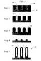
- FIG. 7A detailed diagram of one exemplary process for providing such orientation control is shown in FIG. 7 .
- steps 1 and 2the process still entails the deposition and ordering of a BCP film 80 on a substrate 82 and removal of one of the two polymer components 83 and 84 to form well-ordered deposition spots 86 .
- steps 2 to 6once the substrate 82 is exposed, further etching is conducted to provide orientation recesses 88 .
- Such etchingmay entail metal etching, and polymer and/or SiO 2 RIE.
- orientation recessesare etched in the substrate the metal catalyst 90 can be sputter or vacuum deposited onto the substrate, as shown in step 7 .
- step 8once the metal catalyst is deposited, the remaining polymer component 84 is removed by any conventional means leaving only the metal catalyst deposited within the orientation recesses 88 .
- the size of the PMMA regions, and therefore the size of the ultimate carbon nanotubesdepends on the size of the PS and PMMA block in the BCP molecules.
- the size of the nanotube-nucleating metal particlescan be determined by controlling the length of the BCP block associated with the catalytic metal, while their separation can be controlled by varying the length of the other block.
- BCP'scan be synthesized with a wide range of lengths of the two polymer blocks, making available a similar range of nanotube diameters and separations in the resulting nanotube arrays.
- the diameter of the PMMA cylindersvaries as the length of the PMMA block is increased or decreased, while the “size” of the PS matrix walls, i.e., the separation between the PMMA cylinders, is determined by the length of the PS block.
- P(S-b-MMA)a polystyrene polymethylmethacrylate block copolymer
- blocka polystyrene polymethylmethacrylate block copolymer
- Such a range of PS and PMMA blocksgenerally result in PMMA cylinders having diameters from about 10 to about 100 nm hexagonally packed in a PS matrix with a lattice spacing constant of about 10 to 100 nm.
- P(S-b-MMA)composed of a PS block approximately 300 monomers long connected to a PMMA block about 100 monomers long, was found to self-assemble into arrays of PMMA cylinders having diameters of 14 nm hexagonally packed in a PS matrix with a lattice constant of 24 nm.
- P(S-b-MMA)can be easily synthesized with a wide range of lengths of the two polymer blocks, making available a similar range of nanotube diameters and separations in the resulting nanotube arrays.
- the inventionis also directed to a nano-array formed from one of the processes discussed above, and although in the embodiments shown in FIGS. 1 to 3 , the array of nanotubes comprises periodic rows of uniform nanotubes attached to the substrate, any other arrangement of nanotubes can be utilized such as, for example, staggered arrays of uniform nano-features or uniform rows of nanotubes having alternating sizes. In another alternative embodiment the spacing of the nanotubes may also be varied.
- FIGS. 1 to 3only show an array deposited on a flat substrate surface, any geometry of substrate suitable could be utilized, such as, for example, a curved, corrugated or tubular substrate.
- the design of the array according to the present inventionis necessarily driven by the purpose of the array, and is sensitively dependent on both the geometrical size, shape, orientation and spacing of the nanotubes as well as the size and properties of the array itself.
- the arrayitself has two characteristic sizes: (1) the nano-feature size, or pore size and (2) the nano-feature spacing. Accordingly, although the self-assembled nano-array of the embodiment shown in FIGS.
- 1 to 3comprise a uniform array of uniform cylindrical nanotubes, it should be understood that any shape, size, orientation, or spacing of nanotubes, as described above, can be utilized in the nano-array of the current invention such that the physical properties of the array are suitable for use in a device of interest.
- the nano-structured matrix into which the block copolymer assemblesneed not have the particular cylinders-in-matrix geometry described above in order to be useful.
- a much more common motif for such materialsis for one block to form nm-size spheres, regularly arranged in a 3-dimensional crystalline array within a matrix of the other block.
- Such structurescan also be used as templates for nano-scale patterns on substrates provided that the polymer material can be deposited in a thin enough film so that only one or a few “layers” of the spherical domains are present in the thickness of the film.
- the PS/PB block copolymer referred to aboveis one such material, with the PB blocks forming spherical domains within the PS matrix.
- the self-assembled nano-arrays contemplated in many of the embodiments discussed in the present applicationare constructed of carbon nanotubes made from pyrolizing a carbon-containing feedstock over a substrate having an ordered array of germination points
- the nanofeaturescan be of any shape and made by any process and from any material suitable for making self-assembled nano-features, such as, for example, spheres or pyramids made of other atomic materials or even biomolecules, such as, for example, proteins.
- the nano-featurescan also be further functionalized for a variety of applications, such as, for example, being made hydrophilic or hydrophobic, being charged either negatively or positively, or being derivatized with specific chemical groups, etc.
- the substratecan be made of any material which can withstand the temperatures required for growth of the nanotubes, and which can be modified to provide a suitable ordered array of germination points for growing the nanotubes of the array, such as, for example, silicon, silicon dioxide, metals, alumina, glass, or even polymeric plastics.
- any suitable catalyzing metalcan be used to activate the germination points on the surface of the substrate, such as, for example, iron, nickel or cobalt.
- the catalyzing metalcould be an alloy of two or more metals such as a Co/Ni alloy.
- the metal catalystscould also be produced by pyrolysis of inorganic or organic metal-containing compounds, such as ferric chloride, ferric nitrate or cobalt chloride.
- FeCl 3is repeatedly used as an exemplary metal material, both hydrophilic and hydrophobic metal compounds abound. Examples of the former include all ionic salts of metals, such as chlorides, nitrates, etc.
- hydrophobic metals-containing compoundsexamples include organometallic compounds such as metal carbonyls, metallocenes and acetylacetonates (propanedionates), complexes between the metal atoms and cyclopentadiene (C 5 H 6 ) and 2,4-pentanedione (CH 3 CHOCH 2 CHOCH 3 ), respectively.
- organometallic compoundssuch as metal carbonyls, metallocenes and acetylacetonates (propanedionates), complexes between the metal atoms and cyclopentadiene (C 5 H 6 ) and 2,4-pentanedione (CH 3 CHOCH 2 CHOCH 3 ), respectively.
- an amphiphilic BCPconsisting of blocks of polyethylene oxide (—CH 2 —CH 2 —O—, a hydrophilic monomer) and blocks of polypropylene oxide (—CH 2 —CH(CH 3 )—O—, a hydrophobic monomer) may be used to create nano-porous membranes of ceramics including SiO 2 , Al 2 O 3 , TiO 2 .
- the metal-containing precursorsmay be co-dissolved in alcohol with the BCP such that when the solvent is evaporated, the metal ions associate primarily with the more polar ethylene oxide blocks, which form a matrix through which run cylinders of metal-free polypropylene oxide blocks. This arrangement is then preserved as the material is heated in air to oxidize away the BCP, resulting in a matrix of metal oxide through which runs a regular array of nanometer-scale pores
- the nanofeaturesmay also be semiconducting nanowires, such as solid nanometer-scale wires made of silicon. These silicon nanometer-scale wires are of similar dimensions as the nanotubes and are produced very similarly.
- silicon nanowiresmay be produced by placing the array of catalytic metal dots produced by any of the methods described herein in a reaction vessel containing a reactive silicon containing gas such as silane (SiH 4 ) , rather than methane or ethylene.
- a reactive silicon containing gassuch as silane (SiH 4 )
- the specific catalytic materialsmay be different.
- the catalystis typically gold (Au), rather than iron.
- one block of a copolymermay exhibit differing reactivity from other blocks. Examples include acid-base chemistry, oxidation/reduction chemistry, and solvation. There also exist a large number of block copolymers known to form nano-structured matrices similar to those described herein. Thus a number of possibilities will arise for one skilled in the art for using the self assembling nano-scale structure of block copolymers as a template to create regular arrays of catalytic metal dots on substrate surfaces, and hence to grow regular arrays of nanofeatures for a wide variety of applications.
Landscapes
- Chemical & Material Sciences (AREA)
- Engineering & Computer Science (AREA)
- Nanotechnology (AREA)
- Materials Engineering (AREA)
- Manufacturing & Machinery (AREA)
- Organic Chemistry (AREA)
- Crystallography & Structural Chemistry (AREA)
- General Physics & Mathematics (AREA)
- Condensed Matter Physics & Semiconductors (AREA)
- Physics & Mathematics (AREA)
- Composite Materials (AREA)
- Chemical Kinetics & Catalysis (AREA)
- Inorganic Chemistry (AREA)
- Analytical Chemistry (AREA)
- Microelectronics & Electronic Packaging (AREA)
- Carbon And Carbon Compounds (AREA)
Abstract
Description
This application is a divisional application of U.S. patent application Ser. No. 10/356,299 filed Jan. 30, 2003, now U.S. Pat. No. 7,115,305, issued Oct. 3, 2006, which is based on U.S. application Ser. No. 60/353,290, filed Feb. 1, 2002, the disclosure of which is incorporated by reference.
The U.S. Government has certain rights in this invention pursuant to grant No. NAS 101187-2.1, awarded by the National Aeronautics and Space Administration, Office of Space Science.
The present invention is directed to a method of producing regular arrays of carbon nanotubes, and more particularly to methods of producing regular arrays of carbon nanotubes using self-assembling block-copolymeric materials.
Carbon nanotubes (CNT) have potential uses in a wide array of applications. In particular, regularly spaced arrays of CNTs are expected to have wide ranging applications, either as new and novel devices or as substantial improvements over existing technology. Carbon nanotubes are electrically conductive, have high strength and stiffness, and exhibit electro-mechanical coupling similar to piezo-electric materials: mechanical deformations of a CNT can induce charge transfer into the nanotube, and injected charge can produce deformation or mechanical stress in the nanotube.
These properties combine to give CNTs their versatility in a wide range of uses. One example uses an array of nanotubes as a filter medium in electrophoretic separations of biomolecules. Electrophoretic separation occurs through the differential transport of polyelectrolytes (DNA, proteins, etc.) through a porous medium in the presence of an electric field. The medium acts as a sieve, producing a size-dependent mobility of the molecules. Current state-of-the-art biomolecular analytical systems use polymer gels as sieves. Such gels typically have a wide, random distribution of pore sizes, often extending into size ranges much greater than that of the molecules of interest (1-10 nm), which limits the efficiency of such gels in separations. In addition, polymer gels are susceptible to radiation damage and thermal decomposition, limiting their utility in analysis in harsh environments of interest to NASA. A regularly-spaced array of carbon nanotubes, with well-defined diameters and tube-tube separations in the range of 1-10 nm, is expected to be much more efficient at such separations, much more amenable to miniaturization, and much more tolerant of harsh environments owing to the high stability of CNT. Arrays of CNT would thus advance this technology and make these methods useful in many new environments.
Another set of applications for CNT arrays takes advantage of their mechanical and electrical properties. The high strength and stiffness of these structures makes free-standing CNT excellent candidates for high-Q, high-frequency, nano-scale oscillators. In addition, the electromechanical coupling provides a means by which to either excite vibrations (by applying an RF signal), or to monitor the motions/vibrations of nanotubes by monitoring the current induced as they mechanically oscillate. Arrays of CNT have thus been proposed for use as nanometer-scale RF filters, RF signal detectors and analyzers, and spectrum analyzers for mechanical vibrations (the “electronic ear”). In addition, nanotubes can be functionalized with various chemical substituents to make various molecules bind to them more or less strongly. A nanotube so functionalized would be expected to change its resonant frequency upon the attachment of a target molecule, so that arrays of functionalized nanotubes could also be used as nano-scale chemical sensors (the “electronic nose”).
Finally, the small size and high aspect ratio of CNTs suggests that they will give off electrons by field emission at much lower voltages than the (much larger) metal field emitter tips currently in use. A regular array of independently-addressable nanotubes could thus be used as a low-voltage, low-power array of field emitters, for field emitter displays.
However, all of these applications rely on the ability to produce arrays of nanotubes with regular, well-defined inter-tube spacings. The nanotubes would also need to have their aspect ratios (diameter and wall-thickness vs. length) carefully controlled, to ensure that they stood upright on the substrate, rather than bending over. Many previous studies have reported mats of CNT catalytically grown on smooth substrates. These nanotubes are produced by the decomposition of carbon-containing gases (e.g., C2H4, CO) over nanometer-sized particles of catalytic metals (e.g., Fe, Ni). The nanotubes nucleate upon the metal particles and grow longer as carbon is produced by decomposition of the source gases upon the catalyst. In such studies, catalyst particles are produced by deposition of catalytic metals onto the substrate, either physically or chemically, so that the resultant particles are randomly distributed on the surface and have a wide distribution of sizes. Since the size of growing nanotubes is determined by the size of the catalyst particle from which it nucleates, this process results in growth of nanotubes with a wide diameter distribution, positioned at random upon the substrate surface.
To date, most demonstrations of nanotube growth from such supported catalysts have yielded densely-packed “fields” of nanotubes: neighboring nanotubes are typically in contact with one another, and the size distribution is wide and not well controlled. Clearly, such an “array” does not have the properties needed for the applications discussed above: nanotubes in contact cannot move or be addressed independently, and a wide range of diameters implies a wide range of resonant frequencies, making spectral analysis as described above impossible.
“Bulk” methods for depositing catalytic metals, such as physical or chemical vapor deposition, will result in a stochastic distribution of catalytic particle sizes and locations and thus is not suitable for generating ordered arrays. Lithographic methods, such as photolithography or electron-beam lithography, could work in principle, however photolithography does not have the resolution to make nanometer-sized particles, while conventional e-beam lithography will in general be too slow for large-scale throughput and production of devices using these CNT arrays.
However, recently a technique has been developed for producing geometrically regular self-assembled nanotube arrays with excellent uniformity. This process is based upon the self-organizing formation of highly uniform pore arrays in anodized aluminum films. First, a nanochannel alumina structure is formed by anodizing an aluminum film under conditions that lead to hexagonally-ordered arrays of narrow channels with very high aspect ratios. The nanochannel alumina structure is then used as a template for the growth of nanotube arrays of carbon and other materials, including metals and some semiconductors. The full process technique is disclosed inAppl. Phys. Lett., Vol. 75, pg 367 (1999), and is incorporated herein by reference. Utilizing this technique the authors were able to grow nanotube arrays comprising uniform carbon nanotubes with a diameter of 32 nm. Despite the promise of this new technique, it is a complex procedure, and can provide arrays of CNT with only a narrow range of diameters, limiting its usefulness in some applications.
Accordingly, a need exists for improved method of producing, from catalytic metal particles supported on substrates, an array of nanotubes that are regularly spaced (in particular, they must not be in contact), and which have the same diameter and length (or at least have a very narrow distribution of sizes) in order that they have nearly identical electrical and mechanical properties.
The present invention is directed to a method for producing a uniform array of nano-scale objects utilizing self-assembling block copolymer molecules.
In one particular embodiment, the invention utilizes particular block copolymers to form ordered meso-scale structures, which can then be used to coordinate the formation of regular arrays of nanometer-sized dots of catalytic materials which can serve as nucleation points from which carbon nanotubes can be grown. In such an embodiment, the size and separation of the dots of catalytic material will depend on the size of the polymer blocks.
In still another embodiment, the catalytic dots have dimensions of a few tens of nanometers.
In yet another embodiment, the solution of block copolymer includes catalytic metal compounds designed to associate preferentially with one of the blocks of the block copolymer such that upon formation of the block copolymer meso-scale structure, the catalytic metal compounds form a regular array of regions with high metal content, that can then be used to grow the carbon nanotubes.
In still yet another embodiment, the mixture is spin coated onto a substrate.
In still yet another embodiment, the carbon nanotubes are formed from the decomposition of carbon-containing gases, such as methane, ethylene, acetylene or carbon monoxide.
In still yet another embodiment, the block copolymer meso-scale structure is removed by oxidation to leave only the regular array of dots of catalytic material.
In still yet another embodiment, a mixture of amphiphilic block copolymers and metal compounds having an appropriate associated polarity and/or philicity are utilized. In one such embodiment, the block copolymer monomers used are polystyrene and polymethylmethacrylate, the metal compound is iron chloride, and the substrate is silicon.
In still yet another embodiment, the method of producing the carbon nanotubes involves selectively removing the nanometer-scale structures made from one of the at least two different blocks from the substrate to create a plurality of voids in the polymeric array prior to the application of the catalytic material such that the catalytic material bonds within the voids to form the catalytic material array. In such an embodiment, the step of selectively removing may involve a removal method selected from the group consisting of a UV induced decomposition, reactive ion etching, acid-base reaction, and oxidation.
In still yet another embodiment, the method of producing the carbon nanotubes includes the step of etching an ordered orientation guide recess array into the substrate, from which the orientation of the carbon nanotubes may be controlled. In such a method, the step of etching may involve at least one process selected from the group consisting of metal etching, reactive ion etching, and SiO2etching.
In still yet another embodiment, the invention is directed to a self-assembled nano-array formed according to the block copolymer method described above. In such an embodiment the nano-array may be utilized as filter media in electrophoretic separations, as high-Q high-frequency nano-scale oscillators, nano-meter scale RF filters, RF signal detectors, analyzers, and field emitter tips.
These and other features and advantages of the present invention will be better understood by reference to the following detailed description when considered in conjunction with the accompanying drawings wherein:
The present invention is directed to a method of forming a periodic array of nano-scale objects, such as carbon nanotubes from self-assembling block copolymeric materials.
A generic embodiment of the process for forming ordered carbon nanotube arrays according to the current invention is shown schematically inFIG. 1 . Although the materials used and the exact steps may vary, as shown, there are three general steps in the method for forming nano-arrays according to the present invention: 1) depositing theblock copolymeric material substrate 14 to form an ordered meso-scale structure array of the polymer materials; 2) formation of thecatalytic metal dots 16 based on the meso-scale structure; and 3) growth of thecarbon nanotubes 18 on the catalytic dots to form an orderedarray 20 of carbon nanotubes.
The proposed method makes use of the fact that a certain class of molecules, called. block copolymers, can spontaneously self-assemble into regular arrays of nanometer-scale structures with periodically varying chemical properties.
Block copolymers are polymeric molecules consisting of two or more sections, or “blocks,” each of which consists of a controlled number of monomers of a given type linked together as in a normal polymer molecule. Specifically, certain combinations of block copolymer molecules will, under appropriate conditions, self-assemble into larger, “meso-scale” structures having characteristic dimensions of about 5 to about 100 nanometers. Accordingly, such a polymeric material spontaneously acquires regular structure on a length scale substantially larger than the individual monomer units yet still much smaller than a macroscopic scale.
Using the different polymer blocks of such nanometer-structured materials as local binding agents, it is possible to arrange regular arrays of nanometer-sized dots of catalytic metals from which to grow arrays of carbon nanotubes. For example, using the differential binding properties (such as that arising from the differing polarities) of the polymer blocks with respect to various metal-containing catalytic precursor compounds one can selectively place clusters of catalytic metals in a regular, ordered array.
As briefly discussed above, the present invention relies on the nanoscale separation of BCP materials to form a nanoscale array. Nanoscale phase separation in BCP materials occurs because of the differing affinities, or binding properties, of the various blocks. This separation is driven by the same forces that drive macro-scale phase separations, such as the separation that occurs between oil and water. For example, blocks composed of monomers with polar (hydrophilic) chemical groups will “prefer”, or have an affinity, to be in contact with each other because their energy is lowest in this arrangement because of their dipole interactions. Likewise, blocks composed of non-polar (hydrophobic) monomers will tend to associate with each other because the total energy of the system is lowest in this configuration.
For example, a block copolymer comprising polystyrene (PS) and polymethylmethacrylate (PMMA) blocks of appropriate lengths will, upon heating, undergo a nano-scale phase separation and arrange itself into an arrayed structure consisting of nano-regions of PMMA separated from each other in a matrix of PS. In this system, the separation occurs because the PMMA monomers tend to have large dipole moments arising from the highly polarized oxygen-atom-containing chemical groups present in these monomers. Likewise, the PS monomers are composed only of hydrogen and carbon atoms and so have only very small dipoles.
A first exemplary embodiment of a process for forming the nano-array 20 of the present invention comprising nanotube nano-features utilizing a block copolymer (BCP) technique is shown schematically inFIG. 2 . In a first step, asubstrate 22, such as, for example, silicon is spin-coated with a mixture ofblock copolymer molecules 24 and a metal-containingcatalytic precursor compound 26. Although any such block copolymer capable of self-assembling into larger order array meso-scale structures may be used, in the embodiment shown inFIG. 2 , a block copolymer having blocks of polystyrene (PS) and polymethylmethacrylate (PMMA) is utilized. Likewise, although any suitable metal-containing compound having differential binding affinities for the polymer monomers may be used, in the embodiment shown inFIG. 2 , FeCl3is utilized.
For example, a BCP formed of blocks of both PMMA and PS will have both polar and non-polar chemical groups. Such molecules are said to be “amphiphilic” because they can interact with other molecules of either philicity. Such differences in affinity within BCP molecules are exploited in the current invention to dose selected regions of the BCP with other molecules. Specifically, if ionic or strongly polar metal molecules are mixed with an amphiphilic BCP molecule in solution, these molecules will tend to associate with and bind preferentially with the polar regions of the resulting BCP material when the solvent is removed, because as discussed above the total energy of the system is minimized if charges or dipoles are near each other and can interact strongly. Likewise, if non-polar molecules are co-dissolved with BCP compounds, these molecules will tend to bind to the non-polar areas of the resulting BCP material.
In a second step, the spin-coated mixture is then annealed such that the monomers self-assembled into a well-ordered array structure having regions ofhigh metal content 28 and zerometal content 30.
Instep 3, the BCP matrix is removed, such as by an oxidation process such that only an array ofhigh metal 28 and zerometal content 30 regions remain. In such an embodiment the size and shape of the regions will depend on the size of the associated binding sites of the BCP material.
Instep 4, this regular array ofmetal dots 28 are then used to produce a regular array ofcarbon nanotubes 32. Specifically, the substrate with the array of metal regions is inserted into a furnace or vacuum system through which is flowed an appropriate carbon-containing gas at elevated temperature, such as, for example, methane, ethylene, acetylene, or carbon monoxide gas mixed in argon, nitrogen and/or ammonia at a temperature between about 600 and 900° C. The metal regions serve as nucleation points from which the carbon gases nucleate and growcarbon nanotubes 32. Because the size, shape, orientation, and spacing of the nucleation points may be controlled through the size and number of BCP monomers used, the size, shape, orientation, and spacing of the carbon nanotubes can also be controlled.
A specific example of this process can be described with relation to a mixture of a BCP composed of blocks of PS and PMMA, and FeCl3. In this example, an amphiphilic BCP (PS/PMMA) is mixed with an ionic metal salt (FeCl3) in an amphiphilic solvent, such as, for example, acetone. This solution is spin-coated onto a substrate, and then heated so that the BCP form pillars of PMMA in a PS matrix. Under such conditions, the Fe3+ ions (and Cl− ions) would migrate to the PMMA regions during heating because the abundance of local dipoles in these regions (arising from the oxygen-bearing moieties) tend to attract and bind ionic species. As a result, a regular array of iron-rich and iron free regions with nanometer dimension are formed, which when the polymer is oxidized away, such as by heating to 400° C. in air, leaves an array of Fe particles from which a regular array of carbon nanotubes may be grown.
A second exemplary process for forming the nano-array 40 of the present invention comprising nanotube nano-features utilizing a block copolymer (BCP) technique is shown schematically inFIG. 3 . In a first step, asubstrate 42, such as, for example, silicon is coated with a block copolymer only. Although any block copolymer capable of self-assembling into a meso-scale structured array may be used, in the embodiment shown inFIG. 2 , a BCP consisting of polystyrene (PS) and polymethylmethacrylate (PMMA) is utilized.
The spin-coated polymer layer is then annealed such that the BCP molecules undergo nanoscale phase separation and arrange into an arrayed structure consisting ofcylinders 46 of one monomer separated from each other in amatrix 48 of the second monomer. Using the exemplary materials, annealing would, for example, produce cylinders of PMMA surrounded by a matrix of PS. As in the first exemplary process, the size and separation of the PMMA cylinders would depend on the size of the PS and PMMA blocks in the molecules.
Instep 2, theblock cylinders 46 are removed, such as by an oxidation process. For example, in a PMMA/PS system, this would be done by first exposing the thin film to UV light or high energy electrons, which degrades the PMMA, then washing in acetic acid to remove the degraded PMMA. Although only UV induced process is described above, any synthetic method that takes advantage of this type of differential reactivity between polymer blocks could in principle be used to fabricate nano-scale arrays from block copolymer materials. Additional examples of such potential “differential chemistry” include differential reactivity with respect to reactive ion etching (RIE), acid-base chemistry, and oxidation. Any such scheme could be exploited to preferentially remove one polymer and leave the other present as a template for nano-scale metal deposition. In such an embodiment the size and shape of the regions will depend on the size of the associated binding sites of the BCP material.
As shown instep 3, this process leaves a thin film ofpolystyrene 48 containing a regular array ofholes 50, such that whenmetals 52 are deposited either electrochemically or by vapor deposition onto the surface of the substrate some of the metal is deposited onto the surface of the remaining polymer and some of the metal is deposited into the holes. As in the above embodiment, any suitable metal may be used, such as Co, Ni, Mo, W, Fe, Pd, other transition metals, and alloys thereof. For example, in the embodiment shown inFIG. 3 , Fe is utilized.
Instep 4, thepolystyrene matrix 48 is removed (e.g., by salvation) leaving an array ofmetal dots 52 upon thesubstrate 42.
Instep 5, as in the first exemplary process, this regular array ofmetal dots 52 are then used to produce a regular array ofcarbon nanotubes 54. Specifically, the substrate with the array of metal regions is inserted into a furnace or vacuum system through which is flowed an appropriate carbon-containing gas at elevated temperature, such as, for example, acetylene gas diluted in nitrogen and/or ammonia at about 650° C. The metal regions serve as nucleation points from which the carbon gases nucleate and growcarbon nanotubes 32. Because the size, shape, orientation, and spacing of the nucleation points may be controlled through the size and number of BCP monomers used, the size, shape, orientation, and spacing of the carbon nanotubes can also be controlled.
One example of such technology uses a block copolymer denoted P(S-b-MMA) consisting of a length, or “block,” of polystyrene, typically 100 to 1000 styrene monomers in length, attached to a block of PMMA, typically 50-200 methylmethacrylate monomers long. Using a system comprising P(S-b-MMA) composed of a PS block approximately 300 monomers long connected to a PMMA block about 100 monomers long, produced self-assembled arrays of 14-nm diameter PMMA cylinders hexagonally packed in a PS matrix with a lattice constant of 24 nm.
Specifically, in one embodiment toluene solutions of this P(S-b-MMA) are spin-cast onto substrates, forming films ˜1 micron thick. The nano-structured array spontaneously assemble when the sample is heated to 165° C. (well above the glass transition temperature) for 14 hours in an electric field of 40 V/Cm. Exposure to deep UV light followed by acetic acid rinse will remove the PMMA cylinders and leave a nanoporous PS film with 14 nm pores. These pores are then filled with cobalt metal by electrodeposition, yielding an array of cobalt “nanowires.” The remaining polystyrene matrix is then removed using one of many available techniques including chemical treatment, solvation, oxidation, or RIE. Again, although this scheme utilizes the differential reactivity of the PS and PMMA blocks with respect to UV light/chemical treatment to transfer the nanoscale pattern within the polymer matrix to an underlying substrate, in principle, any block copolymer that forms nano-domains in this way can act as such a template, if the various blocks exhibit differential reactivity under some conditions which can be used to remove one block without affecting the other. For example, differential reactivity with respect to Reactive Ion Etching (RIE) has been used to transfer the nano-structured pattern in a polystyrene/polybutadiene (PS/PB) block copolymer matrix onto a silicon nitride substrate. PS/PB block copolymer forms nano-domains in a manner similar to the P(S-b-MMA) described above, and PB is etched much more rapidly than PS in a CF4plasma. Thus, on a substrate coated with PS/PB and processed with CF4RIE, areas under PB nanostructures can be exposed while those under the surrounding PS matrix remained covered.
Removal of the PS leaves behind a regular array of metal dots with diameters determined by the pore size and heights determined by either film thickness or total flux of incident metal during deposition. Such metal particles are known to nucleate and grow nanotubes under appropriate conditions. Specifically, the substrates with metal dot arrays can be inserted into a furnace or vacuum system, through which is flowed carbon-containing gas molecules, such as C2H4or CO. Upon heating to appropriate temperatures (600-900° C.), the carbon-containing precursor gas molecules will decompose on the catalytic metal surfaces with minimal decomposition on other, non-catalytic regions of the substrate. The carbon generated at each metal particle will arrange into concentric graphitic layers and form a hollow tube, which grows away from the catalyst particle as more carbon is generated by incoming gas molecules.
Although two exemplary methods of producing the ordered carbon nanoarrays are described above, as shown inFIG. 5 a, these methods both described processes in which the catalyst nucleation points70 are deposited on the surface of thesubstrate 72. As shown, under certain circumstances, despite the ordered deposition of the catalyst nucleation points70, the lack of an orientation for the catalyst nucleation points may allow the growth of thecarbon nanotubes 74 to occur in random orientations. An SEM of a carbon nanotube array produced by a conventional growth method without the benefit of an orientation guide is shown inFIG. 6 . However, as shown inFIG. 5 b, the growth and orientation of thecarbon nanotubes 74 can be controlled by providing an initial growth direction, such as by recessing thecatalyst nucleation point 70 into the surface of thesubstrate 72.
A detailed diagram of one exemplary process for providing such orientation control is shown inFIG. 7 . As shown insteps BCP film 80 on asubstrate 82 and removal of one of the twopolymer components steps 2 to6, once thesubstrate 82 is exposed, further etching is conducted to provide orientation recesses88. Such etching may entail metal etching, and polymer and/or SiO2RIE. Once orientation recesses are etched in the substrate themetal catalyst 90 can be sputter or vacuum deposited onto the substrate, as shown instep 7. Finally, as shown instep 8, once the metal catalyst is deposited, the remainingpolymer component 84 is removed by any conventional means leaving only the metal catalyst deposited within the orientation recesses88.
In any of the above described embodiments, the size of the PMMA regions, and therefore the size of the ultimate carbon nanotubes depends on the size of the PS and PMMA block in the BCP molecules. Likewise, in order to form carbon nanotube arrays for a wide variety of applications, it is important to be able to control the spacing of the nanotubes on the substrate. Both of these objectives can be achieved by varying the length of the different blocks in the block copolymer starting material. Specifically, the length of the blocks determines the amount of material, and hence the size, of the features in the nano-structured polymeric material arising from each block. In general, the size of the nanotube-nucleating metal particles can be determined by controlling the length of the BCP block associated with the catalytic metal, while their separation can be controlled by varying the length of the other block. BCP's can be synthesized with a wide range of lengths of the two polymer blocks, making available a similar range of nanotube diameters and separations in the resulting nanotube arrays.
For example, in the PS/PMMA material discussed above, the diameter of the PMMA cylinders varies as the length of the PMMA block is increased or decreased, while the “size” of the PS matrix walls, i.e., the separation between the PMMA cylinders, is determined by the length of the PS block. This exemplary embodiment, as discussed above, uses a polystyrene polymethylmethacrylate block copolymer denoted P(S-b-MMA) consisting of a length, or “block”, of polystyrene, typically 100 to 1000 styrene monomers in length, attached to a block of PMMA, typically 50-200 methylmethacrylate monomers long. Such a range of PS and PMMA blocks generally result in PMMA cylinders having diameters from about 10 to about 100 nm hexagonally packed in a PS matrix with a lattice spacing constant of about 10 to 100 nm. Again, as discussed above, in a recent demonstration using this system, P(S-b-MMA) composed of a PS block approximately 300 monomers long connected to a PMMA block about 100 monomers long, was found to self-assemble into arrays of PMMA cylinders having diameters of 14 nm hexagonally packed in a PS matrix with a lattice constant of 24 nm. However, P(S-b-MMA) can be easily synthesized with a wide range of lengths of the two polymer blocks, making available a similar range of nanotube diameters and separations in the resulting nanotube arrays.
For some applications it is also important to be able to control the location of limited area nanotube arrays. With the present process this can be accomplished by using photomasking to control the area of UV exposure of the block copolymer film, or by using electron beam lithography to control which regions are exposed.
The invention is also directed to a nano-array formed from one of the processes discussed above, and although in the embodiments shown inFIGS. 1 to 3 , the array of nanotubes comprises periodic rows of uniform nanotubes attached to the substrate, any other arrangement of nanotubes can be utilized such as, for example, staggered arrays of uniform nano-features or uniform rows of nanotubes having alternating sizes. In another alternative embodiment the spacing of the nanotubes may also be varied.
Additionally, whileFIGS. 1 to 3 only show an array deposited on a flat substrate surface, any geometry of substrate suitable could be utilized, such as, for example, a curved, corrugated or tubular substrate. It will be understood that the design of the array according to the present invention is necessarily driven by the purpose of the array, and is sensitively dependent on both the geometrical size, shape, orientation and spacing of the nanotubes as well as the size and properties of the array itself. For example, the array itself has two characteristic sizes: (1) the nano-feature size, or pore size and (2) the nano-feature spacing. Accordingly, although the self-assembled nano-array of the embodiment shown inFIGS. 1 to 3 comprise a uniform array of uniform cylindrical nanotubes, it should be understood that any shape, size, orientation, or spacing of nanotubes, as described above, can be utilized in the nano-array of the current invention such that the physical properties of the array are suitable for use in a device of interest.
Moreover, the nano-structured matrix into which the block copolymer assembles need not have the particular cylinders-in-matrix geometry described above in order to be useful. A much more common motif for such materials is for one block to form nm-size spheres, regularly arranged in a 3-dimensional crystalline array within a matrix of the other block. Such structures can also be used as templates for nano-scale patterns on substrates provided that the polymer material can be deposited in a thin enough film so that only one or a few “layers” of the spherical domains are present in the thickness of the film. Indeed, the PS/PB block copolymer referred to above is one such material, with the PB blocks forming spherical domains within the PS matrix.
In turn, while the self-assembled nano-arrays contemplated in many of the embodiments discussed in the present application are constructed of carbon nanotubes made from pyrolizing a carbon-containing feedstock over a substrate having an ordered array of germination points, the nanofeatures can be of any shape and made by any process and from any material suitable for making self-assembled nano-features, such as, for example, spheres or pyramids made of other atomic materials or even biomolecules, such as, for example, proteins. In another embodiment, the nano-features can also be further functionalized for a variety of applications, such as, for example, being made hydrophilic or hydrophobic, being charged either negatively or positively, or being derivatized with specific chemical groups, etc.
Likewise, the substrate can be made of any material which can withstand the temperatures required for growth of the nanotubes, and which can be modified to provide a suitable ordered array of germination points for growing the nanotubes of the array, such as, for example, silicon, silicon dioxide, metals, alumina, glass, or even polymeric plastics.
Any suitable catalyzing metal can be used to activate the germination points on the surface of the substrate, such as, for example, iron, nickel or cobalt. Alternatively, the catalyzing metal could be an alloy of two or more metals such as a Co/Ni alloy. The metal catalysts could also be produced by pyrolysis of inorganic or organic metal-containing compounds, such as ferric chloride, ferric nitrate or cobalt chloride. Moreover, although FeCl3, is repeatedly used as an exemplary metal material, both hydrophilic and hydrophobic metal compounds abound. Examples of the former include all ionic salts of metals, such as chlorides, nitrates, etc. Examples of hydrophobic metals-containing compounds include organometallic compounds such as metal carbonyls, metallocenes and acetylacetonates (propanedionates), complexes between the metal atoms and cyclopentadiene (C5H6) and 2,4-pentanedione (CH3CHOCH2CHOCH3), respectively.
Finally, although only “carbon” containing nanotubes are discussed above, the general method may also be used to make nano-structured metal or semiconductor-containing materials. For example, in one embodiment an amphiphilic BCP consisting of blocks of polyethylene oxide (—CH2—CH2—O—, a hydrophilic monomer) and blocks of polypropylene oxide (—CH2—CH(CH3)—O—, a hydrophobic monomer) may be used to create nano-porous membranes of ceramics including SiO2, Al2O3, TiO2. In such an embodiment, the metal-containing precursors (chloride salts) may be co-dissolved in alcohol with the BCP such that when the solvent is evaporated, the metal ions associate primarily with the more polar ethylene oxide blocks, which form a matrix through which run cylinders of metal-free polypropylene oxide blocks. This arrangement is then preserved as the material is heated in air to oxidize away the BCP, resulting in a matrix of metal oxide through which runs a regular array of nanometer-scale pores
In another embodiment, the nanofeatures may also be semiconducting nanowires, such as solid nanometer-scale wires made of silicon. These silicon nanometer-scale wires are of similar dimensions as the nanotubes and are produced very similarly. For example, in one embodiment silicon nanowires may be produced by placing the array of catalytic metal dots produced by any of the methods described herein in a reaction vessel containing a reactive silicon containing gas such as silane (SiH4) , rather than methane or ethylene. Although the same method may be used to produce the ordered array of catalytic metal dots, the specific catalytic materials may be different. For example, for a silicon nanowire, the catalyst is typically gold (Au), rather than iron.
Although specific embodiments are disclosed herein, it is expected that persons skilled in the art can and will design alternative methods to produce the carbon nanotube arrays that are within the scope of the following claims either literally or under the Doctrine of Equivalents.
Specifically, there are many different chemical conditions under which one block of a copolymer may exhibit differing reactivity from other blocks. Examples include acid-base chemistry, oxidation/reduction chemistry, and solvation. There also exist a large number of block copolymers known to form nano-structured matrices similar to those described herein. Thus a number of possibilities will arise for one skilled in the art for using the self assembling nano-scale structure of block copolymers as a template to create regular arrays of catalytic metal dots on substrate surfaces, and hence to grow regular arrays of nanofeatures for a wide variety of applications.
Claims (41)
1. A method of forming an ordered array of nanofeatures comprising the steps of:
depositing a block copolymer on a substrate, wherein the block copolymer comprises at least two different blocks, and wherein the block copolymer can self-assemble into an ordered polymeric array of a plurality of regular nanometer-scale structures;
activating the block-copolymer to self-assemble to form the polymeric array;
selectively removing the nanometer-scale structures made from one of the at least two different blocks from the substrate to create a plurality of voids in the polymeric array;
applying a catalytic material such that the catalytic material bonds within the voids to form a catalytic material array, wherein the catalytic material is chosen such that an ordered catalytic material array is formed comprising a plurality of catalytic nucleation regions and having a structure defined by the polymeric array;
removing the polymeric array from the substrate such that only the catalytic material array remains; and
growing nanofeatures on the catalytic material array to form an ordered nanofeature array having a structure defined by the catalytic material array.
2. The method described inclaim 1 , wherein the step of selectively removing comprises a removal method selected from the group consisting of UV induced decomposition, solvation, reactive ion etching, acid-base reaction, and oxidation.
3. The method described inclaim 1 , wherein each of the at least two different blocks is made of at least one polymer monomer, and wherein the size, shape, and spacing of the nanometer-scale structures depends on the size and number of the polymer monomers in each of the at least two different blocks.
4. The method described inclaim 1 , wherein the size of the catalytic nucleation regions depends on the length of the block which is selectively removed to form the voids into which the catalytic material bonds.
5. The method described inclaim 1 , wherein spacing between the catalytic nucleation regions depends on a length of the block which is not selectively removed in the formation of the voids into which the catalytic material bonds.
6. The method described inclaim 1 , wherein the at least two different blocks self-assemble based on dipole interactions.
7. The method described inclaim 1 , wherein the block copolymer is an amphiphilic block copolymer.
8. The method described inclaim 1 , wherein the step of depositing comprises spin-coating a solution containing the block copolymer onto the substrate.
9. The method described inclaim 1 , wherein the step of activating includes annealing the polymer coated substrate.
10. The method described inclaim 1 , wherein the step of applying comprises a method selected from one of vapor deposition, sputter deposition, and electrochemical application.
11. The method described inclaim 1 , wherein the step of removing is selected from the group consisting of reactive ion etching, oxidation, and solvation.
12. The method described inclaim 1 , wherein the step of growing the nanofeatures further comprises heating the substrate bearing the catalytic material array under a flow of a carbon-containing gas capable of reacting on the catalytic nucleation regions to form the nanofeatures.
13. The method described inclaim 12 , wherein the step of heating takes place in the presence of an additional gas selected from the group consisting of argon, nitrogen, and ammonia.
14. The method described inclaim 12 , wherein the step of heating takes place in a vacuum chamber at sub-atmospheric pressure.
15. The method described inclaim 12 , wherein the substrate is heated at a temperature of about 600 to about 900° C.
16. The method described inclaim 12 , wherein the carbon-containing gas is selected from the group consisting of methane, ethylene, acetylene, and carbon monoxide.
17. The method described inclaim 1 , further comprising restricting the size of the nanofeature array by a method selected from one of photolitohography, photomasking and electron beam lithography.
18. The method described inclaim 1 , wherein the substrate is a complex shape selected from the group consisting of curve, corrugated and tubular.
19. The method described inclaim 1 , wherein the nanometer-scale structures are selected from one of cylinders and spheres.
20. The method described inclaim 1 , wherein the nanofeatures are a shape selected from the group consisting of tubes, spheres, pyramids and rectangles.
21. The method described inclaim 1 , wherein the nanofeatures are carbon nanotubes.
22. The method described inclaim 21 , wherein the carbon nanotubes have a uniform diameter.
23. The method described inclaim 1 , wherein at least two differently dimensioned nanofeatures are grown on the substrate.
24. The method described inclaim 1 , wherein the nanofeatures have a cross-sectional dimension of about 10 to 100 nm.
25. The method described inclaim 1 , wherein the nanofeature array has a lattice spacing of about 10 to 100 nm.
26. The method described inclaim 1 , wherein the nanofeatures are functionalized.
27. The method described inclaim 1 , wherein the nanofeatures are made from a material selected from the group consisting of metal oxides, silicon, or silicon dioxide.
28. The method described inclaim 1 , wherein the substrate is selected from the group consisting of metals, silicon dioxide, silicon, alumina, glass, and polymeric plastic.
29. The method described inclaim 1 , wherein the catalytic material is selected from the group consisting of Mo, W, Pd, Fe, Ni, Co and a Ni/Co alloy.
30. The method described inclaim 1 , wherein the catalytic material is applied as an ionic metal salt.
31. The method described inclaim 30 , wherein the ionic metal salt is selected from the group consisting of iron chloride, iron nitrate, nickel chloride, nickel nitrate, cobalt chloride, and cobalt nitrate.
32. The method described inclaim 1 , wherein the catalytic material is applied as an organometallic compound.
33. The method described inclaim 32 , wherein the organometallic compound is selected from the group consisting of metal carbonyls, metallocenes, and acetylacetonates.
34. The method described inclaim 1 , wherein the at least two different blocks are polystyrene and polymethylmethacrylate.
35. The method described inclaim 34 , wherein the polystyrene block has a length of about 100 to 1000 styrene monomers.
36. The method described inclaim 34 , wherein the polymethylmethacrylate block has a length of about 50 to 200 methylmethacrylate monomers.
37. The method described inclaim 34 , wherein the nanometer-scale structures comprise polymethylmethacrylate cylinders surrounded by a matrix of polystyrene.
38. The method described inclaim 1 , wherein the nanofeature array is a uniform periodic array having a uniform lattice spacing between nanofeatures.
39. The method described inclaim 1 , wherein the nanofeature array has at least two different lattice spacings.
40. The method described inclaim 1 , further comprising the step of etching an ordered orientation guide recess array comprising a plurality of orientation guide recesses into the substrate prior to applying the catalytic material, such that the structure of the orientation guide array is determined by the polymeric array.
41. The method described inclaim 40 , wherein the step of etching an ordered orientation guide recess array comprises at least one process selected from the group consisting of metal etching, reactive ion etching, and SiO2etching.
Priority Applications (1)
| Application Number | Priority Date | Filing Date | Title |
|---|---|---|---|
| US11/508,514US7700157B2 (en) | 2002-02-01 | 2006-08-22 | Method of producing regular arrays of nano-scale objects using nano-structured block-copolymeric materials |
Applications Claiming Priority (3)
| Application Number | Priority Date | Filing Date | Title |
|---|---|---|---|
| US35329002P | 2002-02-01 | 2002-02-01 | |
| US10/356,299US7115305B2 (en) | 2002-02-01 | 2003-01-30 | Method of producing regular arrays of nano-scale objects using nano-structured block-copolymeric materials |
| US11/508,514US7700157B2 (en) | 2002-02-01 | 2006-08-22 | Method of producing regular arrays of nano-scale objects using nano-structured block-copolymeric materials |
Related Parent Applications (1)
| Application Number | Title | Priority Date | Filing Date |
|---|---|---|---|
| US10/356,299DivisionUS7115305B2 (en) | 2002-02-01 | 2003-01-30 | Method of producing regular arrays of nano-scale objects using nano-structured block-copolymeric materials |
Publications (2)
| Publication Number | Publication Date |
|---|---|
| US20060286297A1 US20060286297A1 (en) | 2006-12-21 |
| US7700157B2true US7700157B2 (en) | 2010-04-20 |
Family
ID=28457035
Family Applications (2)
| Application Number | Title | Priority Date | Filing Date |
|---|---|---|---|
| US10/356,299Expired - Fee RelatedUS7115305B2 (en) | 2002-02-01 | 2003-01-30 | Method of producing regular arrays of nano-scale objects using nano-structured block-copolymeric materials |
| US11/508,514Expired - Fee RelatedUS7700157B2 (en) | 2002-02-01 | 2006-08-22 | Method of producing regular arrays of nano-scale objects using nano-structured block-copolymeric materials |
Family Applications Before (1)
| Application Number | Title | Priority Date | Filing Date |
|---|---|---|---|
| US10/356,299Expired - Fee RelatedUS7115305B2 (en) | 2002-02-01 | 2003-01-30 | Method of producing regular arrays of nano-scale objects using nano-structured block-copolymeric materials |
Country Status (1)
| Country | Link |
|---|---|
| US (2) | US7115305B2 (en) |
Cited By (19)
| Publication number | Priority date | Publication date | Assignee | Title |
|---|---|---|---|---|
| US20080315270A1 (en)* | 2007-06-21 | 2008-12-25 | Micron Technology, Inc. | Multilayer antireflection coatings, structures and devices including the same and methods of making the same |
| US20090014416A1 (en)* | 2000-07-06 | 2009-01-15 | Saint-Gobain Glass France | Transparent textured substrate and methods for obtaining same |
| US20100102415A1 (en)* | 2008-10-28 | 2010-04-29 | Micron Technology, Inc. | Methods for selective permeation of self-assembled block copolymers with metal oxides, methods for forming metal oxide structures, and semiconductor structures including same |
| US8557128B2 (en) | 2007-03-22 | 2013-10-15 | Micron Technology, Inc. | Sub-10 nm line features via rapid graphoepitaxial self-assembly of amphiphilic monolayers |
| US8609221B2 (en) | 2007-06-12 | 2013-12-17 | Micron Technology, Inc. | Alternating self-assembling morphologies of diblock copolymers controlled by variations in surfaces |
| US8633112B2 (en) | 2008-03-21 | 2014-01-21 | Micron Technology, Inc. | Thermal anneal of block copolymer films with top interface constrained to wet both blocks with equal preference |
| US8641914B2 (en) | 2008-03-21 | 2014-02-04 | Micron Technology, Inc. | Methods of improving long range order in self-assembly of block copolymer films with ionic liquids |
| US8642157B2 (en) | 2008-02-13 | 2014-02-04 | Micron Technology, Inc. | One-dimensional arrays of block copolymer cylinders and applications thereof |
| US8753738B2 (en) | 2007-03-06 | 2014-06-17 | Micron Technology, Inc. | Registered structure formation via the application of directed thermal energy to diblock copolymer films |
| US8785559B2 (en) | 2007-06-19 | 2014-07-22 | Micron Technology, Inc. | Crosslinkable graft polymer non-preferentially wetted by polystyrene and polyethylene oxide |
| US20140205531A1 (en)* | 2011-07-26 | 2014-07-24 | Sogang University Research Foundation | Porous carbon particle and producing method of the same |
| US8900963B2 (en) | 2011-11-02 | 2014-12-02 | Micron Technology, Inc. | Methods of forming semiconductor device structures, and related structures |
| US8956713B2 (en) | 2007-04-18 | 2015-02-17 | Micron Technology, Inc. | Methods of forming a stamp and a stamp |
| US8993088B2 (en) | 2008-05-02 | 2015-03-31 | Micron Technology, Inc. | Polymeric materials in self-assembled arrays and semiconductor structures comprising polymeric materials |
| US8999492B2 (en) | 2008-02-05 | 2015-04-07 | Micron Technology, Inc. | Method to produce nanometer-sized features with directed assembly of block copolymers |
| US9087699B2 (en) | 2012-10-05 | 2015-07-21 | Micron Technology, Inc. | Methods of forming an array of openings in a substrate, and related methods of forming a semiconductor device structure |
| US9142420B2 (en) | 2007-04-20 | 2015-09-22 | Micron Technology, Inc. | Extensions of self-assembled structures to increased dimensions via a “bootstrap” self-templating method |
| US9177795B2 (en) | 2013-09-27 | 2015-11-03 | Micron Technology, Inc. | Methods of forming nanostructures including metal oxides |
| US9229328B2 (en) | 2013-05-02 | 2016-01-05 | Micron Technology, Inc. | Methods of forming semiconductor device structures, and related semiconductor device structures |
Families Citing this family (410)
| Publication number | Priority date | Publication date | Assignee | Title |
|---|---|---|---|---|
| US6723299B1 (en) | 2001-05-17 | 2004-04-20 | Zyvex Corporation | System and method for manipulating nanotubes |
| US7115305B2 (en)* | 2002-02-01 | 2006-10-03 | California Institute Of Technology | Method of producing regular arrays of nano-scale objects using nano-structured block-copolymeric materials |
| US20040034177A1 (en) | 2002-05-02 | 2004-02-19 | Jian Chen | Polymer and method for using the polymer for solubilizing nanotubes |
| US6905667B1 (en) | 2002-05-02 | 2005-06-14 | Zyvex Corporation | Polymer and method for using the polymer for noncovalently functionalizing nanotubes |
| AU2003304252A1 (en)* | 2002-06-06 | 2005-01-13 | California Institute Of Technology | Nanocarpets for trapping particulates, bacteria and spores |
| US7037319B2 (en)* | 2002-10-15 | 2006-05-02 | Scimed Life Systems, Inc. | Nanotube paper-based medical device |
| US7491428B2 (en)* | 2002-12-04 | 2009-02-17 | The United States Of America As Represented By The Administrator Of The National Aeronautics And Space Administration | Controlled deposition and alignment of carbon nanotubes |
| US20060124467A1 (en)* | 2003-05-20 | 2006-06-15 | Industrial Technology Research Institute | Metal nanodot arrays and fabrication methods thereof |
| GB2421506B (en) | 2003-05-22 | 2008-07-09 | Zyvex Corp | Nanocomposites and methods thereto |
| WO2005047851A2 (en)* | 2003-10-15 | 2005-05-26 | The Trustees Of Columbia University In The City Of New York | Device for measuring nanometer level pattern-dependent binding reactions |
| FI20045260A7 (en)* | 2003-11-18 | 2005-05-19 | Teknillinen Korkeakoulu | Method for manufacturing a fiber structure |
| US20050151126A1 (en)* | 2003-12-31 | 2005-07-14 | Intel Corporation | Methods of producing carbon nanotubes using peptide or nucleic acid micropatterning |
| US7052618B2 (en)* | 2004-01-28 | 2006-05-30 | Agilent Technologies, Inc. | Nanostructures and methods of making the same |
| KR101065308B1 (en)* | 2004-02-04 | 2011-09-16 | 삼성에스디아이 주식회사 | Photoelectrochemical Cell |
| US6930322B1 (en)* | 2004-03-26 | 2005-08-16 | Matsushita Electric Industrial Co., Ltd. | Combination insulator and organic semiconductor formed from self-assembling block co-polymers |
| US7816655B1 (en)* | 2004-05-21 | 2010-10-19 | Kla-Tencor Technologies Corporation | Reflective electron patterning device and method of using same |
| US8075863B2 (en)* | 2004-05-26 | 2011-12-13 | Massachusetts Institute Of Technology | Methods and devices for growth and/or assembly of nanostructures |
| US7834530B2 (en)* | 2004-05-27 | 2010-11-16 | California Institute Of Technology | Carbon nanotube high-current-density field emitters |
| US7194912B2 (en)* | 2004-07-13 | 2007-03-27 | United States Of America As Represented By The Administrator Of The National Aeronautics And Space Administration | Carbon nanotube-based sensor and method for continually sensing changes in a structure |
| US7296576B2 (en) | 2004-08-18 | 2007-11-20 | Zyvex Performance Materials, Llc | Polymers for enhanced solubility of nanomaterials, compositions and methods therefor |
| US20080090183A1 (en)* | 2004-10-22 | 2008-04-17 | Lingbo Zhu | Aligned Carbon Nanotubes And Method For Construction Thereof |
| TWI463615B (en)* | 2004-11-04 | 2014-12-01 | Taiwan Semiconductor Mfg Co Ltd | Nanotube-based directionally-conductive adhesive |
| US7253008B2 (en)* | 2004-12-28 | 2007-08-07 | Sandia Corporation | Reactive ion etched substrates and methods of making and using |
| CN100437070C (en)* | 2004-12-30 | 2008-11-26 | 清华大学 | Method for fabricating standard leak holes |
| US20060183342A1 (en)* | 2005-02-15 | 2006-08-17 | Eastman Kodak Company | Metal and metal oxide patterned device |
| KR100682864B1 (en)* | 2005-02-19 | 2007-02-15 | 삼성에스디아이 주식회사 | Catalyst layer formation method for carbon nanotube synthesis and carbon nanotube synthesis method using the same |
| US7126207B2 (en)* | 2005-03-24 | 2006-10-24 | Intel Corporation | Capacitor with carbon nanotubes |
| WO2006116687A2 (en)* | 2005-04-27 | 2006-11-02 | The Trustees Of The University Of Pennsylvania | Nanoassays |
| US20060255333A1 (en)* | 2005-05-12 | 2006-11-16 | Kuekes Philip J | Method of forming a controlled distribution of nano-particles on a surface |
| US7278324B2 (en)* | 2005-06-15 | 2007-10-09 | United States Of America As Represented By The Administrator Of The National Aeronautics And Space Administration | Carbon nanotube-based sensor and method for detection of crack growth in a structure |
| US20070183035A1 (en)* | 2005-10-31 | 2007-08-09 | Koji Asakawa | Short-wavelength polarizing elements and the manufacture and use thereof |
| US7960251B2 (en)* | 2005-12-01 | 2011-06-14 | Samsung Electronics Co., Ltd. | Method for producing nanowires using a porous template |
| US8264137B2 (en) | 2006-01-03 | 2012-09-11 | Samsung Electronics Co., Ltd. | Curing binder material for carbon nanotube electron emission cathodes |
| ATE392696T1 (en)* | 2006-01-18 | 2008-05-15 | Consiglio Nazionale Ricerche | NANOMETER DEVICE FOR MEASURING THE CONDUCTIVITY AND QUANTUM EFFECTS OF INDIVIDUAL MOLECULES AND METHOD FOR PRODUCTION AND USE |
| US7893513B2 (en) | 2006-02-02 | 2011-02-22 | William Marsh Rice University | Nanoparticle/nanotube-based nanoelectronic devices and chemically-directed assembly thereof |
| US20070207182A1 (en)* | 2006-03-06 | 2007-09-06 | Jan Weber | Medical devices having electrically aligned elongated particles |
| US7638169B2 (en)* | 2006-03-28 | 2009-12-29 | Intel Corporation | Directing carbon nanotube growth |
| KR101530379B1 (en)* | 2006-03-29 | 2015-06-22 | 삼성전자주식회사 | A method of manufacturing a silicon nanowire using a porous glass template and a device including the silicon nanowire formed thereby |
| CN101432224B (en)* | 2006-04-19 | 2012-06-20 | 独立行政法人科学技术振兴机构 | Manufacture method of substrate with microfine metallic lumps arranged on surface |
| US8052855B2 (en)* | 2006-05-11 | 2011-11-08 | Samsung Electronics Co., Ltd. | Carbon nanotube gas sensor and method of manufacturing the same |
| KR100771886B1 (en) | 2006-09-27 | 2007-11-01 | 삼성전자주식회사 | Method for forming micro contact hole using block copolymer and method for manufacturing semiconductor device |
| US7850941B2 (en)* | 2006-10-20 | 2010-12-14 | General Electric Company | Nanostructure arrays and methods for forming same |
| US20100086464A1 (en)* | 2006-10-20 | 2010-04-08 | General Electric Company | Nanostructure arrays and methods for forming same |
| US8343578B2 (en)* | 2006-10-30 | 2013-01-01 | International Business Machines Corporation | Self-assembled lamellar microdomains and method of alignment |
| EP1946833A1 (en)* | 2006-12-21 | 2008-07-23 | Interuniversitair Microelektronica Centrum | Catalyst nanoparticles for obtaining carbon nanotubes |
| US7678672B2 (en)* | 2007-01-16 | 2010-03-16 | Northrop Grumman Space & Mission Systems Corp. | Carbon nanotube fabrication from crystallography oriented catalyst |
| US8480729B2 (en)* | 2007-09-06 | 2013-07-09 | Boston Science Scimed, Inc. | Medical devices containing silicate and carbon particles |
| US20090169819A1 (en)* | 2007-10-05 | 2009-07-02 | Paul Drzaic | Nanostructure Films |
| US20090091644A1 (en)* | 2007-10-05 | 2009-04-09 | Mackey Jeffrey L | Metallic nanostructure color filter array and method of making the same |
| KR101355167B1 (en) | 2007-12-14 | 2014-01-28 | 삼성전자주식회사 | Method of forming fine pattern using block copolymer having at least three polymer block |
| KR100975656B1 (en) | 2008-07-24 | 2010-08-17 | 한국과학기술원 | Metal catalysts with locally controlled chemical activity and preparation methods thereof |
| KR20110055586A (en)* | 2008-08-05 | 2011-05-25 | 스몰텍 에이비 | Manufacturing method of high aspect ratio template for template and lithography and use of template to drill substrate in nanoscale |
| US8758217B2 (en)* | 2008-09-02 | 2014-06-24 | Georgia Tech Research Corporation | Piezoelectric nanowire vibration sensors |
| KR101055111B1 (en) | 2008-10-28 | 2011-08-09 | 성균관대학교산학협력단 | Carbon nanotube forming method using metal precursor layer, and field emission device manufacturing method |
| US10378106B2 (en) | 2008-11-14 | 2019-08-13 | Asm Ip Holding B.V. | Method of forming insulation film by modified PEALD |
| US8394352B2 (en) | 2008-12-09 | 2013-03-12 | University Of South Carolina | Porous metal oxide particles and their methods of synthesis |
| KR101501609B1 (en)* | 2009-03-16 | 2015-03-11 | 삼성전자주식회사 | METHOD OF COATING METHOD OF CATALYST METAL LAYER USING NUCLEIC ACID |
| US9394608B2 (en) | 2009-04-06 | 2016-07-19 | Asm America, Inc. | Semiconductor processing reactor and components thereof |
| US8802201B2 (en) | 2009-08-14 | 2014-08-12 | Asm America, Inc. | Systems and methods for thin-film deposition of metal oxides using excited nitrogen-oxygen species |
| US8206601B2 (en)* | 2009-12-18 | 2012-06-26 | Hitachi Global Storage Technologies Netherlands B.V. | Supporting membranes on nanometer-scale self-assembled films |
| CN101857460A (en)* | 2010-05-20 | 2010-10-13 | 中国科学院苏州纳米技术与纳米仿生研究所 | Preparation method of carbon nanotube array for spinning |
| US12103844B2 (en) | 2010-06-29 | 2024-10-01 | Korea Advanced Institute Of Science And Technology | Method of fabricating nanostructures using macro pre-patterns |
| US8889245B2 (en)* | 2010-06-29 | 2014-11-18 | Korea Advanced Institute Of Science And Technology | Three-dimensional nanostructures and method for fabricating the same |
| JP5484373B2 (en)* | 2011-02-14 | 2014-05-07 | 東京エレクトロン株式会社 | Pattern formation method |
| US9312155B2 (en) | 2011-06-06 | 2016-04-12 | Asm Japan K.K. | High-throughput semiconductor-processing apparatus equipped with multiple dual-chamber modules |
| US10854498B2 (en) | 2011-07-15 | 2020-12-01 | Asm Ip Holding B.V. | Wafer-supporting device and method for producing same |
| US20130023129A1 (en) | 2011-07-20 | 2013-01-24 | Asm America, Inc. | Pressure transmitter for a semiconductor processing environment |
| EP2760782A4 (en) | 2011-09-28 | 2015-08-19 | Univ Connecticut | METAL OXIDE NANOTIDE NETWORKS ON MONOLITHIC SUBSTRATES |
| US9017481B1 (en) | 2011-10-28 | 2015-04-28 | Asm America, Inc. | Process feed management for semiconductor substrate processing |
| US9659799B2 (en) | 2012-08-28 | 2017-05-23 | Asm Ip Holding B.V. | Systems and methods for dynamic semiconductor process scheduling |
| US20150258531A1 (en)* | 2012-09-14 | 2015-09-17 | University Of Connecticut | Method of Making a Nanotube Array Structure |
| US10714315B2 (en) | 2012-10-12 | 2020-07-14 | Asm Ip Holdings B.V. | Semiconductor reaction chamber showerhead |
| WO2014078807A2 (en)* | 2012-11-19 | 2014-05-22 | The Regents Of The University Of California | Graphene based electrodes and applications |
| US20160376700A1 (en) | 2013-02-01 | 2016-12-29 | Asm Ip Holding B.V. | System for treatment of deposition reactor |
| US20150160072A1 (en)* | 2013-12-06 | 2015-06-11 | Rensselaer Polytechnic Institute | Oriented backscattering wide dynamic-range optical radiation sensor |
| US10683571B2 (en) | 2014-02-25 | 2020-06-16 | Asm Ip Holding B.V. | Gas supply manifold and method of supplying gases to chamber using same |
| US10167557B2 (en) | 2014-03-18 | 2019-01-01 | Asm Ip Holding B.V. | Gas distribution system, reactor including the system, and methods of using the same |
| US11015245B2 (en) | 2014-03-19 | 2021-05-25 | Asm Ip Holding B.V. | Gas-phase reactor and system having exhaust plenum and components thereof |
| US10858737B2 (en) | 2014-07-28 | 2020-12-08 | Asm Ip Holding B.V. | Showerhead assembly and components thereof |
| US9890456B2 (en) | 2014-08-21 | 2018-02-13 | Asm Ip Holding B.V. | Method and system for in situ formation of gas-phase compounds |
| US9657845B2 (en) | 2014-10-07 | 2017-05-23 | Asm Ip Holding B.V. | Variable conductance gas distribution apparatus and method |
| US10941490B2 (en) | 2014-10-07 | 2021-03-09 | Asm Ip Holding B.V. | Multiple temperature range susceptor, assembly, reactor and system including the susceptor, and methods of using the same |
| US10058895B2 (en) | 2014-11-26 | 2018-08-28 | International Business Machines Corporation | Continuous flow, size-based separation of entities down to the nanometer scale using nanopillar arrays |
| US9636675B2 (en) | 2014-11-26 | 2017-05-02 | International Business Machines Corporation | Pillar array structure with uniform and high aspect ratio nanometer gaps |
| KR102263121B1 (en) | 2014-12-22 | 2021-06-09 | 에이에스엠 아이피 홀딩 비.브이. | Semiconductor device and manufacuring method thereof |
| US10529542B2 (en) | 2015-03-11 | 2020-01-07 | Asm Ip Holdings B.V. | Cross-flow reactor and method |
| US10276355B2 (en) | 2015-03-12 | 2019-04-30 | Asm Ip Holding B.V. | Multi-zone reactor, system including the reactor, and method of using the same |
| US10458018B2 (en) | 2015-06-26 | 2019-10-29 | Asm Ip Holding B.V. | Structures including metal carbide material, devices including the structures, and methods of forming same |
| US10600673B2 (en) | 2015-07-07 | 2020-03-24 | Asm Ip Holding B.V. | Magnetic susceptor to baseplate seal |
| US9960072B2 (en) | 2015-09-29 | 2018-05-01 | Asm Ip Holding B.V. | Variable adjustment for precise matching of multiple chamber cavity housings |
| US10211308B2 (en) | 2015-10-21 | 2019-02-19 | Asm Ip Holding B.V. | NbMC layers |
| US11139308B2 (en) | 2015-12-29 | 2021-10-05 | Asm Ip Holding B.V. | Atomic layer deposition of III-V compounds to form V-NAND devices |
| GB201600745D0 (en)* | 2016-01-14 | 2016-03-02 | Univ College Cork Nat Univ Ie | Fabrication of nanopatterned surfaces for application in optical and related device applications |
| US10529554B2 (en) | 2016-02-19 | 2020-01-07 | Asm Ip Holding B.V. | Method for forming silicon nitride film selectively on sidewalls or flat surfaces of trenches |
| US10468251B2 (en) | 2016-02-19 | 2019-11-05 | Asm Ip Holding B.V. | Method for forming spacers using silicon nitride film for spacer-defined multiple patterning |
| US10343920B2 (en)* | 2016-03-18 | 2019-07-09 | Asm Ip Holding B.V. | Aligned carbon nanotubes |
| US10190213B2 (en) | 2016-04-21 | 2019-01-29 | Asm Ip Holding B.V. | Deposition of metal borides |
| US10865475B2 (en) | 2016-04-21 | 2020-12-15 | Asm Ip Holding B.V. | Deposition of metal borides and silicides |
| US10032628B2 (en) | 2016-05-02 | 2018-07-24 | Asm Ip Holding B.V. | Source/drain performance through conformal solid state doping |
| US10367080B2 (en) | 2016-05-02 | 2019-07-30 | Asm Ip Holding B.V. | Method of forming a germanium oxynitride film |
| US11453943B2 (en) | 2016-05-25 | 2022-09-27 | Asm Ip Holding B.V. | Method for forming carbon-containing silicon/metal oxide or nitride film by ALD using silicon precursor and hydrocarbon precursor |
| US10388509B2 (en) | 2016-06-28 | 2019-08-20 | Asm Ip Holding B.V. | Formation of epitaxial layers via dislocation filtering |
| US9859151B1 (en) | 2016-07-08 | 2018-01-02 | Asm Ip Holding B.V. | Selective film deposition method to form air gaps |
| US10612137B2 (en) | 2016-07-08 | 2020-04-07 | Asm Ip Holdings B.V. | Organic reactants for atomic layer deposition |
| US10714385B2 (en) | 2016-07-19 | 2020-07-14 | Asm Ip Holding B.V. | Selective deposition of tungsten |
| US9887082B1 (en) | 2016-07-28 | 2018-02-06 | Asm Ip Holding B.V. | Method and apparatus for filling a gap |
| KR102532607B1 (en) | 2016-07-28 | 2023-05-15 | 에이에스엠 아이피 홀딩 비.브이. | Substrate processing apparatus and method of operating the same |
| US10395919B2 (en) | 2016-07-28 | 2019-08-27 | Asm Ip Holding B.V. | Method and apparatus for filling a gap |
| US9812320B1 (en) | 2016-07-28 | 2017-11-07 | Asm Ip Holding B.V. | Method and apparatus for filling a gap |
| US10410943B2 (en) | 2016-10-13 | 2019-09-10 | Asm Ip Holding B.V. | Method for passivating a surface of a semiconductor and related systems |
| US10643826B2 (en) | 2016-10-26 | 2020-05-05 | Asm Ip Holdings B.V. | Methods for thermally calibrating reaction chambers |
| US11532757B2 (en) | 2016-10-27 | 2022-12-20 | Asm Ip Holding B.V. | Deposition of charge trapping layers |
| US10714350B2 (en) | 2016-11-01 | 2020-07-14 | ASM IP Holdings, B.V. | Methods for forming a transition metal niobium nitride film on a substrate by atomic layer deposition and related semiconductor device structures |
| US10435790B2 (en) | 2016-11-01 | 2019-10-08 | Asm Ip Holding B.V. | Method of subatmospheric plasma-enhanced ALD using capacitively coupled electrodes with narrow gap |
| US10229833B2 (en) | 2016-11-01 | 2019-03-12 | Asm Ip Holding B.V. | Methods for forming a transition metal nitride film on a substrate by atomic layer deposition and related semiconductor device structures |
| US10134757B2 (en) | 2016-11-07 | 2018-11-20 | Asm Ip Holding B.V. | Method of processing a substrate and a device manufactured by using the method |
| KR102546317B1 (en) | 2016-11-15 | 2023-06-21 | 에이에스엠 아이피 홀딩 비.브이. | Gas supply unit and substrate processing apparatus including the same |
| US10340135B2 (en) | 2016-11-28 | 2019-07-02 | Asm Ip Holding B.V. | Method of topologically restricted plasma-enhanced cyclic deposition of silicon or metal nitride |
| KR102762543B1 (en) | 2016-12-14 | 2025-02-05 | 에이에스엠 아이피 홀딩 비.브이. | Substrate processing apparatus |
| US11447861B2 (en) | 2016-12-15 | 2022-09-20 | Asm Ip Holding B.V. | Sequential infiltration synthesis apparatus and a method of forming a patterned structure |
| US11581186B2 (en) | 2016-12-15 | 2023-02-14 | Asm Ip Holding B.V. | Sequential infiltration synthesis apparatus |
| KR102700194B1 (en) | 2016-12-19 | 2024-08-28 | 에이에스엠 아이피 홀딩 비.브이. | Substrate processing apparatus |
| US10269558B2 (en) | 2016-12-22 | 2019-04-23 | Asm Ip Holding B.V. | Method of forming a structure on a substrate |
| US10867788B2 (en) | 2016-12-28 | 2020-12-15 | Asm Ip Holding B.V. | Method of forming a structure on a substrate |
| US11390950B2 (en) | 2017-01-10 | 2022-07-19 | Asm Ip Holding B.V. | Reactor system and method to reduce residue buildup during a film deposition process |
| US10655221B2 (en) | 2017-02-09 | 2020-05-19 | Asm Ip Holding B.V. | Method for depositing oxide film by thermal ALD and PEALD |
| US10468261B2 (en) | 2017-02-15 | 2019-11-05 | Asm Ip Holding B.V. | Methods for forming a metallic film on a substrate by cyclical deposition and related semiconductor device structures |
| US10529563B2 (en) | 2017-03-29 | 2020-01-07 | Asm Ip Holdings B.V. | Method for forming doped metal oxide films on a substrate by cyclical deposition and related semiconductor device structures |
| KR102457289B1 (en) | 2017-04-25 | 2022-10-21 | 에이에스엠 아이피 홀딩 비.브이. | Method for depositing a thin film and manufacturing a semiconductor device |
| US10770286B2 (en) | 2017-05-08 | 2020-09-08 | Asm Ip Holdings B.V. | Methods for selectively forming a silicon nitride film on a substrate and related semiconductor device structures |
| US10892156B2 (en) | 2017-05-08 | 2021-01-12 | Asm Ip Holding B.V. | Methods for forming a silicon nitride film on a substrate and related semiconductor device structures |
| US10446393B2 (en) | 2017-05-08 | 2019-10-15 | Asm Ip Holding B.V. | Methods for forming silicon-containing epitaxial layers and related semiconductor device structures |
| US10504742B2 (en) | 2017-05-31 | 2019-12-10 | Asm Ip Holding B.V. | Method of atomic layer etching using hydrogen plasma |
| US11623206B2 (en) | 2017-06-01 | 2023-04-11 | University Of Connecticut | Manganese-cobalt spinel oxide nanowire arrays |
| US10886123B2 (en) | 2017-06-02 | 2021-01-05 | Asm Ip Holding B.V. | Methods for forming low temperature semiconductor layers and related semiconductor device structures |
| US11691123B2 (en) | 2017-06-02 | 2023-07-04 | University Of Connecticut | Low-temperature diesel oxidation catalysts using TiO2 nanowire arrays integrated on a monolithic substrate |
| US11465129B2 (en) | 2017-06-06 | 2022-10-11 | University Of Connecticut | Microwave assisted and low-temperature fabrication of nanowire arrays on scalable 2D and 3D substrates |
| US12040200B2 (en) | 2017-06-20 | 2024-07-16 | Asm Ip Holding B.V. | Semiconductor processing apparatus and methods for calibrating a semiconductor processing apparatus |
| US11306395B2 (en) | 2017-06-28 | 2022-04-19 | Asm Ip Holding B.V. | Methods for depositing a transition metal nitride film on a substrate by atomic layer deposition and related deposition apparatus |
| US10685834B2 (en) | 2017-07-05 | 2020-06-16 | Asm Ip Holdings B.V. | Methods for forming a silicon germanium tin layer and related semiconductor device structures |
| KR20190009245A (en) | 2017-07-18 | 2019-01-28 | 에이에스엠 아이피 홀딩 비.브이. | Methods for forming a semiconductor device structure and related semiconductor device structures |
| US11374112B2 (en) | 2017-07-19 | 2022-06-28 | Asm Ip Holding B.V. | Method for depositing a group IV semiconductor and related semiconductor device structures |
| US10541333B2 (en) | 2017-07-19 | 2020-01-21 | Asm Ip Holding B.V. | Method for depositing a group IV semiconductor and related semiconductor device structures |
| US11018002B2 (en) | 2017-07-19 | 2021-05-25 | Asm Ip Holding B.V. | Method for selectively depositing a Group IV semiconductor and related semiconductor device structures |
| US10590535B2 (en) | 2017-07-26 | 2020-03-17 | Asm Ip Holdings B.V. | Chemical treatment, deposition and/or infiltration apparatus and method for using the same |
| US10605530B2 (en) | 2017-07-26 | 2020-03-31 | Asm Ip Holding B.V. | Assembly of a liner and a flange for a vertical furnace as well as the liner and the vertical furnace |
| TWI815813B (en) | 2017-08-04 | 2023-09-21 | 荷蘭商Asm智慧財產控股公司 | Showerhead assembly for distributing a gas within a reaction chamber |
| US10770336B2 (en) | 2017-08-08 | 2020-09-08 | Asm Ip Holding B.V. | Substrate lift mechanism and reactor including same |
| US10692741B2 (en) | 2017-08-08 | 2020-06-23 | Asm Ip Holdings B.V. | Radiation shield |
| US10249524B2 (en) | 2017-08-09 | 2019-04-02 | Asm Ip Holding B.V. | Cassette holder assembly for a substrate cassette and holding member for use in such assembly |
| US11769682B2 (en) | 2017-08-09 | 2023-09-26 | Asm Ip Holding B.V. | Storage apparatus for storing cassettes for substrates and processing apparatus equipped therewith |
| US11139191B2 (en) | 2017-08-09 | 2021-10-05 | Asm Ip Holding B.V. | Storage apparatus for storing cassettes for substrates and processing apparatus equipped therewith |
| USD900036S1 (en) | 2017-08-24 | 2020-10-27 | Asm Ip Holding B.V. | Heater electrical connector and adapter |
| US11830730B2 (en) | 2017-08-29 | 2023-11-28 | Asm Ip Holding B.V. | Layer forming method and apparatus |
| KR102491945B1 (en) | 2017-08-30 | 2023-01-26 | 에이에스엠 아이피 홀딩 비.브이. | Substrate processing apparatus |
| US11056344B2 (en) | 2017-08-30 | 2021-07-06 | Asm Ip Holding B.V. | Layer forming method |
| US11295980B2 (en) | 2017-08-30 | 2022-04-05 | Asm Ip Holding B.V. | Methods for depositing a molybdenum metal film over a dielectric surface of a substrate by a cyclical deposition process and related semiconductor device structures |
| KR102401446B1 (en) | 2017-08-31 | 2022-05-24 | 에이에스엠 아이피 홀딩 비.브이. | Substrate processing apparatus |
| US10607895B2 (en) | 2017-09-18 | 2020-03-31 | Asm Ip Holdings B.V. | Method for forming a semiconductor device structure comprising a gate fill metal |
| KR102630301B1 (en) | 2017-09-21 | 2024-01-29 | 에이에스엠 아이피 홀딩 비.브이. | Method of sequential infiltration synthesis treatment of infiltrateable material and structures and devices formed using same |
| US10844484B2 (en) | 2017-09-22 | 2020-11-24 | Asm Ip Holding B.V. | Apparatus for dispensing a vapor phase reactant to a reaction chamber and related methods |
| US10658205B2 (en) | 2017-09-28 | 2020-05-19 | Asm Ip Holdings B.V. | Chemical dispensing apparatus and methods for dispensing a chemical to a reaction chamber |
| US10403504B2 (en) | 2017-10-05 | 2019-09-03 | Asm Ip Holding B.V. | Method for selectively depositing a metallic film on a substrate |
| US10319588B2 (en) | 2017-10-10 | 2019-06-11 | Asm Ip Holding B.V. | Method for depositing a metal chalcogenide on a substrate by cyclical deposition |
| US10923344B2 (en) | 2017-10-30 | 2021-02-16 | Asm Ip Holding B.V. | Methods for forming a semiconductor structure and related semiconductor structures |
| KR102443047B1 (en) | 2017-11-16 | 2022-09-14 | 에이에스엠 아이피 홀딩 비.브이. | Method of processing a substrate and a device manufactured by the same |
| US10910262B2 (en) | 2017-11-16 | 2021-02-02 | Asm Ip Holding B.V. | Method of selectively depositing a capping layer structure on a semiconductor device structure |
| US11022879B2 (en) | 2017-11-24 | 2021-06-01 | Asm Ip Holding B.V. | Method of forming an enhanced unexposed photoresist layer |
| CN111344522B (en) | 2017-11-27 | 2022-04-12 | 阿斯莫Ip控股公司 | Including clean mini-environment device |
| WO2019103613A1 (en) | 2017-11-27 | 2019-05-31 | Asm Ip Holding B.V. | A storage device for storing wafer cassettes for use with a batch furnace |
| US10872771B2 (en) | 2018-01-16 | 2020-12-22 | Asm Ip Holding B. V. | Method for depositing a material film on a substrate within a reaction chamber by a cyclical deposition process and related device structures |
| KR102695659B1 (en) | 2018-01-19 | 2024-08-14 | 에이에스엠 아이피 홀딩 비.브이. | Method for depositing a gap filling layer by plasma assisted deposition |
| TWI799494B (en) | 2018-01-19 | 2023-04-21 | 荷蘭商Asm 智慧財產控股公司 | Deposition method |
| USD903477S1 (en) | 2018-01-24 | 2020-12-01 | Asm Ip Holdings B.V. | Metal clamp |
| US11018047B2 (en) | 2018-01-25 | 2021-05-25 | Asm Ip Holding B.V. | Hybrid lift pin |
| USD880437S1 (en) | 2018-02-01 | 2020-04-07 | Asm Ip Holding B.V. | Gas supply plate for semiconductor manufacturing apparatus |
| US10535516B2 (en) | 2018-02-01 | 2020-01-14 | Asm Ip Holdings B.V. | Method for depositing a semiconductor structure on a surface of a substrate and related semiconductor structures |
| US11081345B2 (en) | 2018-02-06 | 2021-08-03 | Asm Ip Holding B.V. | Method of post-deposition treatment for silicon oxide film |
| WO2019158960A1 (en) | 2018-02-14 | 2019-08-22 | Asm Ip Holding B.V. | A method for depositing a ruthenium-containing film on a substrate by a cyclical deposition process |
| US10896820B2 (en) | 2018-02-14 | 2021-01-19 | Asm Ip Holding B.V. | Method for depositing a ruthenium-containing film on a substrate by a cyclical deposition process |
| US10731249B2 (en) | 2018-02-15 | 2020-08-04 | Asm Ip Holding B.V. | Method of forming a transition metal containing film on a substrate by a cyclical deposition process, a method for supplying a transition metal halide compound to a reaction chamber, and related vapor deposition apparatus |
| KR102636427B1 (en) | 2018-02-20 | 2024-02-13 | 에이에스엠 아이피 홀딩 비.브이. | Substrate processing method and apparatus |
| US10658181B2 (en) | 2018-02-20 | 2020-05-19 | Asm Ip Holding B.V. | Method of spacer-defined direct patterning in semiconductor fabrication |
| US10975470B2 (en) | 2018-02-23 | 2021-04-13 | Asm Ip Holding B.V. | Apparatus for detecting or monitoring for a chemical precursor in a high temperature environment |
| US11473195B2 (en) | 2018-03-01 | 2022-10-18 | Asm Ip Holding B.V. | Semiconductor processing apparatus and a method for processing a substrate |
| US11629406B2 (en) | 2018-03-09 | 2023-04-18 | Asm Ip Holding B.V. | Semiconductor processing apparatus comprising one or more pyrometers for measuring a temperature of a substrate during transfer of the substrate |
| US11114283B2 (en) | 2018-03-16 | 2021-09-07 | Asm Ip Holding B.V. | Reactor, system including the reactor, and methods of manufacturing and using same |
| KR102646467B1 (en) | 2018-03-27 | 2024-03-11 | 에이에스엠 아이피 홀딩 비.브이. | Method of forming an electrode on a substrate and a semiconductor device structure including an electrode |
| US11230766B2 (en) | 2018-03-29 | 2022-01-25 | Asm Ip Holding B.V. | Substrate processing apparatus and method |
| US10510536B2 (en) | 2018-03-29 | 2019-12-17 | Asm Ip Holding B.V. | Method of depositing a co-doped polysilicon film on a surface of a substrate within a reaction chamber |
| US11088002B2 (en) | 2018-03-29 | 2021-08-10 | Asm Ip Holding B.V. | Substrate rack and a substrate processing system and method |
| KR102501472B1 (en) | 2018-03-30 | 2023-02-20 | 에이에스엠 아이피 홀딩 비.브이. | Substrate processing method |
| KR102600229B1 (en) | 2018-04-09 | 2023-11-10 | 에이에스엠 아이피 홀딩 비.브이. | Substrate supporting device, substrate processing apparatus including the same and substrate processing method |
| US12025484B2 (en) | 2018-05-08 | 2024-07-02 | Asm Ip Holding B.V. | Thin film forming method |
| TWI811348B (en) | 2018-05-08 | 2023-08-11 | 荷蘭商Asm 智慧財產控股公司 | Methods for depositing an oxide film on a substrate by a cyclical deposition process and related device structures |
| US12272527B2 (en) | 2018-05-09 | 2025-04-08 | Asm Ip Holding B.V. | Apparatus for use with hydrogen radicals and method of using same |
| KR20190129718A (en) | 2018-05-11 | 2019-11-20 | 에이에스엠 아이피 홀딩 비.브이. | Methods for forming a doped metal carbide film on a substrate and related semiconductor device structures |
| KR102596988B1 (en) | 2018-05-28 | 2023-10-31 | 에이에스엠 아이피 홀딩 비.브이. | Method of processing a substrate and a device manufactured by the same |
| TWI840362B (en) | 2018-06-04 | 2024-05-01 | 荷蘭商Asm Ip私人控股有限公司 | Wafer handling chamber with moisture reduction |
| US11718913B2 (en) | 2018-06-04 | 2023-08-08 | Asm Ip Holding B.V. | Gas distribution system and reactor system including same |
| US11286562B2 (en) | 2018-06-08 | 2022-03-29 | Asm Ip Holding B.V. | Gas-phase chemical reactor and method of using same |
| KR102568797B1 (en) | 2018-06-21 | 2023-08-21 | 에이에스엠 아이피 홀딩 비.브이. | Substrate processing system |
| US10797133B2 (en) | 2018-06-21 | 2020-10-06 | Asm Ip Holding B.V. | Method for depositing a phosphorus doped silicon arsenide film and related semiconductor device structures |
| TWI873894B (en) | 2018-06-27 | 2025-02-21 | 荷蘭商Asm Ip私人控股有限公司 | Cyclic deposition methods for forming metal-containing material and films and structures including the metal-containing material |
| KR102854019B1 (en) | 2018-06-27 | 2025-09-02 | 에이에스엠 아이피 홀딩 비.브이. | Periodic deposition method for forming a metal-containing material and films and structures comprising the metal-containing material |
| KR102686758B1 (en) | 2018-06-29 | 2024-07-18 | 에이에스엠 아이피 홀딩 비.브이. | Method for depositing a thin film and manufacturing a semiconductor device |
| US10612136B2 (en) | 2018-06-29 | 2020-04-07 | ASM IP Holding, B.V. | Temperature-controlled flange and reactor system including same |
| US10388513B1 (en) | 2018-07-03 | 2019-08-20 | Asm Ip Holding B.V. | Method for depositing silicon-free carbon-containing film as gap-fill layer by pulse plasma-assisted deposition |
| US10755922B2 (en) | 2018-07-03 | 2020-08-25 | Asm Ip Holding B.V. | Method for depositing silicon-free carbon-containing film as gap-fill layer by pulse plasma-assisted deposition |
| US10767789B2 (en) | 2018-07-16 | 2020-09-08 | Asm Ip Holding B.V. | Diaphragm valves, valve components, and methods for forming valve components |
| US10483099B1 (en) | 2018-07-26 | 2019-11-19 | Asm Ip Holding B.V. | Method for forming thermally stable organosilicon polymer film |
| US11053591B2 (en) | 2018-08-06 | 2021-07-06 | Asm Ip Holding B.V. | Multi-port gas injection system and reactor system including same |
| US10883175B2 (en) | 2018-08-09 | 2021-01-05 | Asm Ip Holding B.V. | Vertical furnace for processing substrates and a liner for use therein |
| US10829852B2 (en) | 2018-08-16 | 2020-11-10 | Asm Ip Holding B.V. | Gas distribution device for a wafer processing apparatus |
| US11430674B2 (en) | 2018-08-22 | 2022-08-30 | Asm Ip Holding B.V. | Sensor array, apparatus for dispensing a vapor phase reactant to a reaction chamber and related methods |
| KR102707956B1 (en) | 2018-09-11 | 2024-09-19 | 에이에스엠 아이피 홀딩 비.브이. | Method for deposition of a thin film |
| US11024523B2 (en) | 2018-09-11 | 2021-06-01 | Asm Ip Holding B.V. | Substrate processing apparatus and method |
| US11049751B2 (en) | 2018-09-14 | 2021-06-29 | Asm Ip Holding B.V. | Cassette supply system to store and handle cassettes and processing apparatus equipped therewith |
| CN110970344B (en) | 2018-10-01 | 2024-10-25 | Asmip控股有限公司 | Substrate holding apparatus, system comprising the same and method of using the same |
| US11232963B2 (en) | 2018-10-03 | 2022-01-25 | Asm Ip Holding B.V. | Substrate processing apparatus and method |
| KR102592699B1 (en) | 2018-10-08 | 2023-10-23 | 에이에스엠 아이피 홀딩 비.브이. | Substrate support unit and apparatuses for depositing thin film and processing the substrate including the same |
| US10847365B2 (en) | 2018-10-11 | 2020-11-24 | Asm Ip Holding B.V. | Method of forming conformal silicon carbide film by cyclic CVD |
| US10811256B2 (en) | 2018-10-16 | 2020-10-20 | Asm Ip Holding B.V. | Method for etching a carbon-containing feature |
| KR102546322B1 (en) | 2018-10-19 | 2023-06-21 | 에이에스엠 아이피 홀딩 비.브이. | Substrate processing apparatus and substrate processing method |
| KR102605121B1 (en) | 2018-10-19 | 2023-11-23 | 에이에스엠 아이피 홀딩 비.브이. | Substrate processing apparatus and substrate processing method |
| USD948463S1 (en) | 2018-10-24 | 2022-04-12 | Asm Ip Holding B.V. | Susceptor for semiconductor substrate supporting apparatus |
| US10381219B1 (en) | 2018-10-25 | 2019-08-13 | Asm Ip Holding B.V. | Methods for forming a silicon nitride film |
| US12378665B2 (en) | 2018-10-26 | 2025-08-05 | Asm Ip Holding B.V. | High temperature coatings for a preclean and etch apparatus and related methods |
| US11087997B2 (en) | 2018-10-31 | 2021-08-10 | Asm Ip Holding B.V. | Substrate processing apparatus for processing substrates |
| KR102748291B1 (en) | 2018-11-02 | 2024-12-31 | 에이에스엠 아이피 홀딩 비.브이. | Substrate support unit and substrate processing apparatus including the same |
| US11572620B2 (en) | 2018-11-06 | 2023-02-07 | Asm Ip Holding B.V. | Methods for selectively depositing an amorphous silicon film on a substrate |
| US11031242B2 (en) | 2018-11-07 | 2021-06-08 | Asm Ip Holding B.V. | Methods for depositing a boron doped silicon germanium film |
| US10847366B2 (en) | 2018-11-16 | 2020-11-24 | Asm Ip Holding B.V. | Methods for depositing a transition metal chalcogenide film on a substrate by a cyclical deposition process |
| US10818758B2 (en) | 2018-11-16 | 2020-10-27 | Asm Ip Holding B.V. | Methods for forming a metal silicate film on a substrate in a reaction chamber and related semiconductor device structures |
| US10559458B1 (en) | 2018-11-26 | 2020-02-11 | Asm Ip Holding B.V. | Method of forming oxynitride film |
| WO2020111755A1 (en) | 2018-11-27 | 2020-06-04 | 경희대학교산학협력단 | Field emission tomosynthesis system, emitter thereof and preparation method thereof |
| US12040199B2 (en) | 2018-11-28 | 2024-07-16 | Asm Ip Holding B.V. | Substrate processing apparatus for processing substrates |
| US11217444B2 (en) | 2018-11-30 | 2022-01-04 | Asm Ip Holding B.V. | Method for forming an ultraviolet radiation responsive metal oxide-containing film |
| KR102636428B1 (en) | 2018-12-04 | 2024-02-13 | 에이에스엠 아이피 홀딩 비.브이. | A method for cleaning a substrate processing apparatus |
| US11158513B2 (en) | 2018-12-13 | 2021-10-26 | Asm Ip Holding B.V. | Methods for forming a rhenium-containing film on a substrate by a cyclical deposition process and related semiconductor device structures |
| TWI874340B (en) | 2018-12-14 | 2025-03-01 | 荷蘭商Asm Ip私人控股有限公司 | Method of forming device structure, structure formed by the method and system for performing the method |
| TWI866480B (en) | 2019-01-17 | 2024-12-11 | 荷蘭商Asm Ip 私人控股有限公司 | Methods of forming a transition metal containing film on a substrate by a cyclical deposition process |
| KR102727227B1 (en) | 2019-01-22 | 2024-11-07 | 에이에스엠 아이피 홀딩 비.브이. | Semiconductor processing device |
| CN111524788B (en) | 2019-02-01 | 2023-11-24 | Asm Ip私人控股有限公司 | Method for forming topologically selective films of silicon oxide |
| KR102626263B1 (en) | 2019-02-20 | 2024-01-16 | 에이에스엠 아이피 홀딩 비.브이. | Cyclical deposition method including treatment step and apparatus for same |
| TWI873122B (en) | 2019-02-20 | 2025-02-21 | 荷蘭商Asm Ip私人控股有限公司 | Method of filling a recess formed within a surface of a substrate, semiconductor structure formed according to the method, and semiconductor processing apparatus |
| TWI845607B (en) | 2019-02-20 | 2024-06-21 | 荷蘭商Asm Ip私人控股有限公司 | Cyclical deposition method and apparatus for filling a recess formed within a substrate surface |
| TWI838458B (en) | 2019-02-20 | 2024-04-11 | 荷蘭商Asm Ip私人控股有限公司 | Apparatus and methods for plug fill deposition in 3-d nand applications |
| TWI842826B (en) | 2019-02-22 | 2024-05-21 | 荷蘭商Asm Ip私人控股有限公司 | Substrate processing apparatus and method for processing substrate |
| KR102782593B1 (en) | 2019-03-08 | 2025-03-14 | 에이에스엠 아이피 홀딩 비.브이. | Structure Including SiOC Layer and Method of Forming Same |
| KR102858005B1 (en) | 2019-03-08 | 2025-09-09 | 에이에스엠 아이피 홀딩 비.브이. | Method for Selective Deposition of Silicon Nitride Layer and Structure Including Selectively-Deposited Silicon Nitride Layer |
| US11742198B2 (en) | 2019-03-08 | 2023-08-29 | Asm Ip Holding B.V. | Structure including SiOCN layer and method of forming same |
| JP2020167398A (en) | 2019-03-28 | 2020-10-08 | エーエスエム・アイピー・ホールディング・ベー・フェー | Door openers and substrate processing equipment provided with door openers |
| KR102809999B1 (en) | 2019-04-01 | 2025-05-19 | 에이에스엠 아이피 홀딩 비.브이. | Method of manufacturing semiconductor device |
| KR20200123380A (en) | 2019-04-19 | 2020-10-29 | 에이에스엠 아이피 홀딩 비.브이. | Layer forming method and apparatus |
| KR20200125453A (en) | 2019-04-24 | 2020-11-04 | 에이에스엠 아이피 홀딩 비.브이. | Gas-phase reactor system and method of using same |
| KR20200130121A (en) | 2019-05-07 | 2020-11-18 | 에이에스엠 아이피 홀딩 비.브이. | Chemical source vessel with dip tube |
| US11289326B2 (en) | 2019-05-07 | 2022-03-29 | Asm Ip Holding B.V. | Method for reforming amorphous carbon polymer film |
| KR20200130652A (en) | 2019-05-10 | 2020-11-19 | 에이에스엠 아이피 홀딩 비.브이. | Method of depositing material onto a surface and structure formed according to the method |
| JP7612342B2 (en) | 2019-05-16 | 2025-01-14 | エーエスエム・アイピー・ホールディング・ベー・フェー | Wafer boat handling apparatus, vertical batch furnace and method |
| JP7598201B2 (en) | 2019-05-16 | 2024-12-11 | エーエスエム・アイピー・ホールディング・ベー・フェー | Wafer boat handling apparatus, vertical batch furnace and method |
| USD975665S1 (en) | 2019-05-17 | 2023-01-17 | Asm Ip Holding B.V. | Susceptor shaft |
| USD947913S1 (en) | 2019-05-17 | 2022-04-05 | Asm Ip Holding B.V. | Susceptor shaft |
| USD935572S1 (en) | 2019-05-24 | 2021-11-09 | Asm Ip Holding B.V. | Gas channel plate |
| USD922229S1 (en) | 2019-06-05 | 2021-06-15 | Asm Ip Holding B.V. | Device for controlling a temperature of a gas supply unit |
| KR20200141002A (en) | 2019-06-06 | 2020-12-17 | 에이에스엠 아이피 홀딩 비.브이. | Method of using a gas-phase reactor system including analyzing exhausted gas |
| KR20200141931A (en) | 2019-06-10 | 2020-12-21 | 에이에스엠 아이피 홀딩 비.브이. | Method for cleaning quartz epitaxial chambers |
| KR20200143254A (en) | 2019-06-11 | 2020-12-23 | 에이에스엠 아이피 홀딩 비.브이. | Method of forming an electronic structure using an reforming gas, system for performing the method, and structure formed using the method |
| USD944946S1 (en) | 2019-06-14 | 2022-03-01 | Asm Ip Holding B.V. | Shower plate |
| USD931978S1 (en) | 2019-06-27 | 2021-09-28 | Asm Ip Holding B.V. | Showerhead vacuum transport |
| KR20210005515A (en) | 2019-07-03 | 2021-01-14 | 에이에스엠 아이피 홀딩 비.브이. | Temperature control assembly for substrate processing apparatus and method of using same |
| JP7499079B2 (en) | 2019-07-09 | 2024-06-13 | エーエスエム・アイピー・ホールディング・ベー・フェー | Plasma device using coaxial waveguide and substrate processing method |
| CN112216646A (en) | 2019-07-10 | 2021-01-12 | Asm Ip私人控股有限公司 | Substrate supporting assembly and substrate processing device comprising same |
| KR20210010307A (en) | 2019-07-16 | 2021-01-27 | 에이에스엠 아이피 홀딩 비.브이. | Substrate processing apparatus |
| KR102860110B1 (en) | 2019-07-17 | 2025-09-16 | 에이에스엠 아이피 홀딩 비.브이. | Methods of forming silicon germanium structures |
| KR20210010816A (en) | 2019-07-17 | 2021-01-28 | 에이에스엠 아이피 홀딩 비.브이. | Radical assist ignition plasma system and method |
| US11643724B2 (en) | 2019-07-18 | 2023-05-09 | Asm Ip Holding B.V. | Method of forming structures using a neutral beam |
| TWI839544B (en) | 2019-07-19 | 2024-04-21 | 荷蘭商Asm Ip私人控股有限公司 | Method of forming topology-controlled amorphous carbon polymer film |
| KR20210010817A (en) | 2019-07-19 | 2021-01-28 | 에이에스엠 아이피 홀딩 비.브이. | Method of Forming Topology-Controlled Amorphous Carbon Polymer Film |
| TWI851767B (en) | 2019-07-29 | 2024-08-11 | 荷蘭商Asm Ip私人控股有限公司 | Methods for selective deposition utilizing n-type dopants and/or alternative dopants to achieve high dopant incorporation |
| US12169361B2 (en) | 2019-07-30 | 2024-12-17 | Asm Ip Holding B.V. | Substrate processing apparatus and method |
| CN112309899A (en) | 2019-07-30 | 2021-02-02 | Asm Ip私人控股有限公司 | Substrate processing apparatus |
| CN112309900A (en) | 2019-07-30 | 2021-02-02 | Asm Ip私人控股有限公司 | Substrate processing apparatus |
| US11587814B2 (en) | 2019-07-31 | 2023-02-21 | Asm Ip Holding B.V. | Vertical batch furnace assembly |
| US11227782B2 (en) | 2019-07-31 | 2022-01-18 | Asm Ip Holding B.V. | Vertical batch furnace assembly |
| US11587815B2 (en) | 2019-07-31 | 2023-02-21 | Asm Ip Holding B.V. | Vertical batch furnace assembly |
| CN112323048B (en) | 2019-08-05 | 2024-02-09 | Asm Ip私人控股有限公司 | Liquid level sensor for chemical source container |
| CN112342526A (en) | 2019-08-09 | 2021-02-09 | Asm Ip私人控股有限公司 | Heater assembly including cooling device and method of using same |
| USD965524S1 (en) | 2019-08-19 | 2022-10-04 | Asm Ip Holding B.V. | Susceptor support |
| USD965044S1 (en) | 2019-08-19 | 2022-09-27 | Asm Ip Holding B.V. | Susceptor shaft |
| JP2021031769A (en) | 2019-08-21 | 2021-03-01 | エーエスエム アイピー ホールディング ビー.ブイ. | Production apparatus of mixed gas of film deposition raw material and film deposition apparatus |
| KR20210024423A (en) | 2019-08-22 | 2021-03-05 | 에이에스엠 아이피 홀딩 비.브이. | Method for forming a structure with a hole |
| USD930782S1 (en) | 2019-08-22 | 2021-09-14 | Asm Ip Holding B.V. | Gas distributor |
| USD979506S1 (en) | 2019-08-22 | 2023-02-28 | Asm Ip Holding B.V. | Insulator |
| USD949319S1 (en) | 2019-08-22 | 2022-04-19 | Asm Ip Holding B.V. | Exhaust duct |
| USD940837S1 (en) | 2019-08-22 | 2022-01-11 | Asm Ip Holding B.V. | Electrode |
| US11286558B2 (en) | 2019-08-23 | 2022-03-29 | Asm Ip Holding B.V. | Methods for depositing a molybdenum nitride film on a surface of a substrate by a cyclical deposition process and related semiconductor device structures including a molybdenum nitride film |
| KR20210024420A (en) | 2019-08-23 | 2021-03-05 | 에이에스엠 아이피 홀딩 비.브이. | Method for depositing silicon oxide film having improved quality by peald using bis(diethylamino)silane |
| KR102806450B1 (en) | 2019-09-04 | 2025-05-12 | 에이에스엠 아이피 홀딩 비.브이. | Methods for selective deposition using a sacrificial capping layer |
| KR102733104B1 (en) | 2019-09-05 | 2024-11-22 | 에이에스엠 아이피 홀딩 비.브이. | Substrate processing apparatus |
| US11562901B2 (en) | 2019-09-25 | 2023-01-24 | Asm Ip Holding B.V. | Substrate processing method |
| CN112593212B (en) | 2019-10-02 | 2023-12-22 | Asm Ip私人控股有限公司 | Method for forming topologically selective silicon oxide film by cyclic plasma enhanced deposition process |
| TW202128273A (en) | 2019-10-08 | 2021-08-01 | 荷蘭商Asm Ip私人控股有限公司 | Gas injection system, reactor system, and method of depositing material on surface of substratewithin reaction chamber |
| KR20210042810A (en) | 2019-10-08 | 2021-04-20 | 에이에스엠 아이피 홀딩 비.브이. | Reactor system including a gas distribution assembly for use with activated species and method of using same |
| TWI846953B (en) | 2019-10-08 | 2024-07-01 | 荷蘭商Asm Ip私人控股有限公司 | Substrate processing device |
| TWI846966B (en) | 2019-10-10 | 2024-07-01 | 荷蘭商Asm Ip私人控股有限公司 | Method of forming a photoresist underlayer and structure including same |
| US12009241B2 (en) | 2019-10-14 | 2024-06-11 | Asm Ip Holding B.V. | Vertical batch furnace assembly with detector to detect cassette |
| TWI834919B (en) | 2019-10-16 | 2024-03-11 | 荷蘭商Asm Ip私人控股有限公司 | Method of topology-selective film formation of silicon oxide |
| US11637014B2 (en) | 2019-10-17 | 2023-04-25 | Asm Ip Holding B.V. | Methods for selective deposition of doped semiconductor material |
| KR102845724B1 (en) | 2019-10-21 | 2025-08-13 | 에이에스엠 아이피 홀딩 비.브이. | Apparatus and methods for selectively etching films |
| KR20210050453A (en) | 2019-10-25 | 2021-05-07 | 에이에스엠 아이피 홀딩 비.브이. | Methods for filling a gap feature on a substrate surface and related semiconductor structures |
| US11646205B2 (en) | 2019-10-29 | 2023-05-09 | Asm Ip Holding B.V. | Methods of selectively forming n-type doped material on a surface, systems for selectively forming n-type doped material, and structures formed using same |
| KR20210054983A (en) | 2019-11-05 | 2021-05-14 | 에이에스엠 아이피 홀딩 비.브이. | Structures with doped semiconductor layers and methods and systems for forming same |
| US11501968B2 (en) | 2019-11-15 | 2022-11-15 | Asm Ip Holding B.V. | Method for providing a semiconductor device with silicon filled gaps |
| KR102861314B1 (en) | 2019-11-20 | 2025-09-17 | 에이에스엠 아이피 홀딩 비.브이. | Method of depositing carbon-containing material on a surface of a substrate, structure formed using the method, and system for forming the structure |
| CN112951697B (en) | 2019-11-26 | 2025-07-29 | Asmip私人控股有限公司 | Substrate processing apparatus |
| US11450529B2 (en) | 2019-11-26 | 2022-09-20 | Asm Ip Holding B.V. | Methods for selectively forming a target film on a substrate comprising a first dielectric surface and a second metallic surface |
| CN120432376A (en) | 2019-11-29 | 2025-08-05 | Asm Ip私人控股有限公司 | Substrate processing apparatus |
| CN112885692B (en) | 2019-11-29 | 2025-08-15 | Asmip私人控股有限公司 | Substrate processing apparatus |
| JP7527928B2 (en) | 2019-12-02 | 2024-08-05 | エーエスエム・アイピー・ホールディング・ベー・フェー | Substrate processing apparatus and substrate processing method |
| KR20210070898A (en) | 2019-12-04 | 2021-06-15 | 에이에스엠 아이피 홀딩 비.브이. | Substrate processing apparatus |
| KR20210078405A (en) | 2019-12-17 | 2021-06-28 | 에이에스엠 아이피 홀딩 비.브이. | Method of forming vanadium nitride layer and structure including the vanadium nitride layer |
| KR20210080214A (en) | 2019-12-19 | 2021-06-30 | 에이에스엠 아이피 홀딩 비.브이. | Methods for filling a gap feature on a substrate and related semiconductor structures |
| JP7730637B2 (en) | 2020-01-06 | 2025-08-28 | エーエスエム・アイピー・ホールディング・ベー・フェー | Gas delivery assembly, components thereof, and reactor system including same |
| JP7636892B2 (en) | 2020-01-06 | 2025-02-27 | エーエスエム・アイピー・ホールディング・ベー・フェー | Channeled Lift Pins |
| US11993847B2 (en) | 2020-01-08 | 2024-05-28 | Asm Ip Holding B.V. | Injector |
| KR20210093163A (en) | 2020-01-16 | 2021-07-27 | 에이에스엠 아이피 홀딩 비.브이. | Method of forming high aspect ratio features |
| KR102675856B1 (en) | 2020-01-20 | 2024-06-17 | 에이에스엠 아이피 홀딩 비.브이. | Method of forming thin film and method of modifying surface of thin film |
| TWI889744B (en) | 2020-01-29 | 2025-07-11 | 荷蘭商Asm Ip私人控股有限公司 | Contaminant trap system, and baffle plate stack |
| TW202513845A (en) | 2020-02-03 | 2025-04-01 | 荷蘭商Asm Ip私人控股有限公司 | Semiconductor structures and methods for forming the same |
| KR20210100010A (en) | 2020-02-04 | 2021-08-13 | 에이에스엠 아이피 홀딩 비.브이. | Method and apparatus for transmittance measurements of large articles |
| US11776846B2 (en) | 2020-02-07 | 2023-10-03 | Asm Ip Holding B.V. | Methods for depositing gap filling fluids and related systems and devices |
| KR20210103956A (en) | 2020-02-13 | 2021-08-24 | 에이에스엠 아이피 홀딩 비.브이. | Substrate processing apparatus including light receiving device and calibration method of light receiving device |
| TW202146691A (en) | 2020-02-13 | 2021-12-16 | 荷蘭商Asm Ip私人控股有限公司 | Gas distribution assembly, shower plate assembly, and method of adjusting conductance of gas to reaction chamber |
| TWI855223B (en) | 2020-02-17 | 2024-09-11 | 荷蘭商Asm Ip私人控股有限公司 | Method for growing phosphorous-doped silicon layer |
| CN113410160A (en) | 2020-02-28 | 2021-09-17 | Asm Ip私人控股有限公司 | System specially used for cleaning parts |
| KR20210113043A (en) | 2020-03-04 | 2021-09-15 | 에이에스엠 아이피 홀딩 비.브이. | Alignment fixture for a reactor system |
| KR20210116240A (en) | 2020-03-11 | 2021-09-27 | 에이에스엠 아이피 홀딩 비.브이. | Substrate handling device with adjustable joints |
| US11876356B2 (en) | 2020-03-11 | 2024-01-16 | Asm Ip Holding B.V. | Lockout tagout assembly and system and method of using same |
| KR102775390B1 (en) | 2020-03-12 | 2025-02-28 | 에이에스엠 아이피 홀딩 비.브이. | Method for Fabricating Layer Structure Having Target Topological Profile |
| US12173404B2 (en) | 2020-03-17 | 2024-12-24 | Asm Ip Holding B.V. | Method of depositing epitaxial material, structure formed using the method, and system for performing the method |
| KR102755229B1 (en) | 2020-04-02 | 2025-01-14 | 에이에스엠 아이피 홀딩 비.브이. | Thin film forming method |
| TWI887376B (en) | 2020-04-03 | 2025-06-21 | 荷蘭商Asm Ip私人控股有限公司 | Method for manufacturing semiconductor device |
| TWI888525B (en) | 2020-04-08 | 2025-07-01 | 荷蘭商Asm Ip私人控股有限公司 | Apparatus and methods for selectively etching silcon oxide films |
| KR20210128343A (en) | 2020-04-15 | 2021-10-26 | 에이에스엠 아이피 홀딩 비.브이. | Method of forming chromium nitride layer and structure including the chromium nitride layer |
| US11821078B2 (en) | 2020-04-15 | 2023-11-21 | Asm Ip Holding B.V. | Method for forming precoat film and method for forming silicon-containing film |
| US11996289B2 (en) | 2020-04-16 | 2024-05-28 | Asm Ip Holding B.V. | Methods of forming structures including silicon germanium and silicon layers, devices formed using the methods, and systems for performing the methods |
| KR20210130646A (en) | 2020-04-21 | 2021-11-01 | 에이에스엠 아이피 홀딩 비.브이. | Method for processing a substrate |
| KR20210132612A (en) | 2020-04-24 | 2021-11-04 | 에이에스엠 아이피 홀딩 비.브이. | Methods and apparatus for stabilizing vanadium compounds |
| KR102866804B1 (en) | 2020-04-24 | 2025-09-30 | 에이에스엠 아이피 홀딩 비.브이. | Vertical batch furnace assembly comprising a cooling gas supply |
| CN113555279A (en) | 2020-04-24 | 2021-10-26 | Asm Ip私人控股有限公司 | Methods of forming vanadium nitride-containing layers and structures comprising the same |
| TW202208671A (en) | 2020-04-24 | 2022-03-01 | 荷蘭商Asm Ip私人控股有限公司 | Methods of forming structures including vanadium boride and vanadium phosphide layers |
| KR20210132600A (en) | 2020-04-24 | 2021-11-04 | 에이에스엠 아이피 홀딩 비.브이. | Methods and systems for depositing a layer comprising vanadium, nitrogen, and a further element |
| KR102783898B1 (en) | 2020-04-29 | 2025-03-18 | 에이에스엠 아이피 홀딩 비.브이. | Solid source precursor vessel |
| KR20210134869A (en) | 2020-05-01 | 2021-11-11 | 에이에스엠 아이피 홀딩 비.브이. | Fast FOUP swapping with a FOUP handler |
| JP7726664B2 (en) | 2020-05-04 | 2025-08-20 | エーエスエム・アイピー・ホールディング・ベー・フェー | Substrate processing system for processing a substrate |
| KR102788543B1 (en) | 2020-05-13 | 2025-03-27 | 에이에스엠 아이피 홀딩 비.브이. | Laser alignment fixture for a reactor system |
| TW202146699A (en) | 2020-05-15 | 2021-12-16 | 荷蘭商Asm Ip私人控股有限公司 | Method of forming a silicon germanium layer, semiconductor structure, semiconductor device, method of forming a deposition layer, and deposition system |
| KR20210143653A (en) | 2020-05-19 | 2021-11-29 | 에이에스엠 아이피 홀딩 비.브이. | Substrate processing apparatus |
| KR20210145079A (en) | 2020-05-21 | 2021-12-01 | 에이에스엠 아이피 홀딩 비.브이. | Flange and apparatus for processing substrates |
| KR102795476B1 (en) | 2020-05-21 | 2025-04-11 | 에이에스엠 아이피 홀딩 비.브이. | Structures including multiple carbon layers and methods of forming and using same |
| TWI873343B (en) | 2020-05-22 | 2025-02-21 | 荷蘭商Asm Ip私人控股有限公司 | Reaction system for forming thin film on substrate |
| KR20210146802A (en) | 2020-05-26 | 2021-12-06 | 에이에스엠 아이피 홀딩 비.브이. | Method for depositing boron and gallium containing silicon germanium layers |
| TWI876048B (en) | 2020-05-29 | 2025-03-11 | 荷蘭商Asm Ip私人控股有限公司 | Substrate processing device |
| TW202212620A (en) | 2020-06-02 | 2022-04-01 | 荷蘭商Asm Ip私人控股有限公司 | Apparatus for processing substrate, method of forming film, and method of controlling apparatus for processing substrate |
| CN111929277B (en)* | 2020-06-03 | 2021-06-01 | 中国科学院苏州生物医学工程技术研究所 | One-dimensional Assemblies of Precious Metal Nanoparticles with Tunable Spacing and Their Applications in Nanosensors |
| TW202208659A (en) | 2020-06-16 | 2022-03-01 | 荷蘭商Asm Ip私人控股有限公司 | Method for depositing boron containing silicon germanium layers |
| TW202218133A (en) | 2020-06-24 | 2022-05-01 | 荷蘭商Asm Ip私人控股有限公司 | Method for forming a layer provided with silicon |
| TWI873359B (en) | 2020-06-30 | 2025-02-21 | 荷蘭商Asm Ip私人控股有限公司 | Substrate processing method |
| US12431354B2 (en) | 2020-07-01 | 2025-09-30 | Asm Ip Holding B.V. | Silicon nitride and silicon oxide deposition methods using fluorine inhibitor |
| TW202202649A (en) | 2020-07-08 | 2022-01-16 | 荷蘭商Asm Ip私人控股有限公司 | Substrate processing method |
| KR20220010438A (en) | 2020-07-17 | 2022-01-25 | 에이에스엠 아이피 홀딩 비.브이. | Structures and methods for use in photolithography |
| TWI878570B (en) | 2020-07-20 | 2025-04-01 | 荷蘭商Asm Ip私人控股有限公司 | Method and system for depositing molybdenum layers |
| KR20220011092A (en) | 2020-07-20 | 2022-01-27 | 에이에스엠 아이피 홀딩 비.브이. | Method and system for forming structures including transition metal layers |
| KR102160445B1 (en)* | 2020-07-22 | 2020-09-29 | 경희대학교 산학협력단 | Emitter for x-ray tube and manufacturing method thereof |
| US12322591B2 (en) | 2020-07-27 | 2025-06-03 | Asm Ip Holding B.V. | Thin film deposition process |
| KR20220021863A (en) | 2020-08-14 | 2022-02-22 | 에이에스엠 아이피 홀딩 비.브이. | Method for processing a substrate |
| US12040177B2 (en) | 2020-08-18 | 2024-07-16 | Asm Ip Holding B.V. | Methods for forming a laminate film by cyclical plasma-enhanced deposition processes |
| TW202228863A (en) | 2020-08-25 | 2022-08-01 | 荷蘭商Asm Ip私人控股有限公司 | Method for cleaning a substrate, method for selectively depositing, and reaction system |
| US11725280B2 (en) | 2020-08-26 | 2023-08-15 | Asm Ip Holding B.V. | Method for forming metal silicon oxide and metal silicon oxynitride layers |
| TW202229601A (en) | 2020-08-27 | 2022-08-01 | 荷蘭商Asm Ip私人控股有限公司 | Method of forming patterned structures, method of manipulating mechanical property, device structure, and substrate processing system |
| TW202217045A (en) | 2020-09-10 | 2022-05-01 | 荷蘭商Asm Ip私人控股有限公司 | Methods for depositing gap filing fluids and related systems and devices |
| USD990534S1 (en) | 2020-09-11 | 2023-06-27 | Asm Ip Holding B.V. | Weighted lift pin |
| KR20220036866A (en) | 2020-09-16 | 2022-03-23 | 에이에스엠 아이피 홀딩 비.브이. | Silicon oxide deposition method |
| USD1012873S1 (en) | 2020-09-24 | 2024-01-30 | Asm Ip Holding B.V. | Electrode for semiconductor processing apparatus |
| TWI889903B (en) | 2020-09-25 | 2025-07-11 | 荷蘭商Asm Ip私人控股有限公司 | Semiconductor processing method |
| US12009224B2 (en) | 2020-09-29 | 2024-06-11 | Asm Ip Holding B.V. | Apparatus and method for etching metal nitrides |
| KR20220045900A (en) | 2020-10-06 | 2022-04-13 | 에이에스엠 아이피 홀딩 비.브이. | Deposition method and an apparatus for depositing a silicon-containing material |
| CN114293174A (en) | 2020-10-07 | 2022-04-08 | Asm Ip私人控股有限公司 | Gas supply unit and substrate processing apparatus including the same |
| TW202229613A (en) | 2020-10-14 | 2022-08-01 | 荷蘭商Asm Ip私人控股有限公司 | Method of depositing material on stepped structure |
| TW202232565A (en) | 2020-10-15 | 2022-08-16 | 荷蘭商Asm Ip私人控股有限公司 | Method of manufacturing semiconductor device, and substrate treatment apparatus using ether-cat |
| TW202217037A (en) | 2020-10-22 | 2022-05-01 | 荷蘭商Asm Ip私人控股有限公司 | Method of depositing vanadium metal, structure, device and a deposition assembly |
| TW202223136A (en) | 2020-10-28 | 2022-06-16 | 荷蘭商Asm Ip私人控股有限公司 | Method for forming layer on substrate, and semiconductor processing system |
| TW202229620A (en) | 2020-11-12 | 2022-08-01 | 特文特大學 | Deposition system, method for controlling reaction condition, method for depositing |
| TW202229795A (en) | 2020-11-23 | 2022-08-01 | 荷蘭商Asm Ip私人控股有限公司 | A substrate processing apparatus with an injector |
| TW202235649A (en) | 2020-11-24 | 2022-09-16 | 荷蘭商Asm Ip私人控股有限公司 | Methods for filling a gap and related systems and devices |
| TW202235675A (en) | 2020-11-30 | 2022-09-16 | 荷蘭商Asm Ip私人控股有限公司 | Injector, and substrate processing apparatus |
| US12255053B2 (en) | 2020-12-10 | 2025-03-18 | Asm Ip Holding B.V. | Methods and systems for depositing a layer |
| TW202233884A (en) | 2020-12-14 | 2022-09-01 | 荷蘭商Asm Ip私人控股有限公司 | Method of forming structures for threshold voltage control |
| US11946137B2 (en) | 2020-12-16 | 2024-04-02 | Asm Ip Holding B.V. | Runout and wobble measurement fixtures |
| TW202232639A (en) | 2020-12-18 | 2022-08-16 | 荷蘭商Asm Ip私人控股有限公司 | Wafer processing apparatus with a rotatable table |
| TW202242184A (en) | 2020-12-22 | 2022-11-01 | 荷蘭商Asm Ip私人控股有限公司 | Precursor capsule, precursor vessel, vapor deposition assembly, and method of loading solid precursor into precursor vessel |
| TW202231903A (en) | 2020-12-22 | 2022-08-16 | 荷蘭商Asm Ip私人控股有限公司 | Transition metal deposition method, transition metal layer, and deposition assembly for depositing transition metal on substrate |
| TW202226899A (en) | 2020-12-22 | 2022-07-01 | 荷蘭商Asm Ip私人控股有限公司 | Plasma treatment device having matching box |
| USD980814S1 (en) | 2021-05-11 | 2023-03-14 | Asm Ip Holding B.V. | Gas distributor for substrate processing apparatus |
| USD981973S1 (en) | 2021-05-11 | 2023-03-28 | Asm Ip Holding B.V. | Reactor wall for substrate processing apparatus |
| USD980813S1 (en) | 2021-05-11 | 2023-03-14 | Asm Ip Holding B.V. | Gas flow control plate for substrate processing apparatus |
| USD1023959S1 (en) | 2021-05-11 | 2024-04-23 | Asm Ip Holding B.V. | Electrode for substrate processing apparatus |
| USD990441S1 (en) | 2021-09-07 | 2023-06-27 | Asm Ip Holding B.V. | Gas flow control plate |
| USD1060598S1 (en) | 2021-12-03 | 2025-02-04 | Asm Ip Holding B.V. | Split showerhead cover |
Citations (80)
| Publication number | Priority date | Publication date | Assignee | Title |
|---|---|---|---|---|
| US3955015A (en) | 1972-10-23 | 1976-05-04 | Nippon Selfoc Co., Ltd. | Method of manufacturing a transparent light conducting element of synthetic resin having refractive index gradient |
| US4104204A (en) | 1974-08-09 | 1978-08-01 | Temple University | Photosensitization of oxygen to the singlet excited state using ion exchange resin to which is attached a dye and photooxidative waste water treatment |
| US4173475A (en) | 1977-05-31 | 1979-11-06 | Bell Telephone Laboratories, Incorporated | Latent image thick refractive index recordings |
| US4173474A (en) | 1976-07-27 | 1979-11-06 | Canon Kabushiki Kaisha | Hologram and method of production using two solvent treatments |
| US4260725A (en) | 1979-12-10 | 1981-04-07 | Bausch & Lomb Incorporated | Hydrophilic contact lens made from polysiloxanes which are thermally bonded to polymerizable groups and which contain hydrophilic sidechains |
| US4330383A (en) | 1978-07-18 | 1982-05-18 | Polymer Technology Corporation | Dimensionally stable oxygen permeable hard contact lens material and method of manufacture |
| JPS60175009A (en) | 1984-02-21 | 1985-09-09 | Nippon Sheet Glass Co Ltd | Production of plastic optical element having refractive index distribution |
| JPS6127501A (en) | 1984-07-17 | 1986-02-07 | Nippon Sheet Glass Co Ltd | Manufacture of synthetic resin optical element having refractive index distribution |
| US4575373A (en) | 1984-11-02 | 1986-03-11 | Johnson Don R | Laser adjustable intraocular lens and method of altering lens power |
| DE3605512A1 (en) | 1985-02-20 | 1986-08-21 | Central Glass Co., Ltd., Ube, Yamaguchi | FLUORINE RESIN COMPOSITION FOR OPTICAL USE |
| US4685921A (en) | 1986-02-24 | 1987-08-11 | Peyman Gholam A | Variable refractive power, expandable intraocular lenses |
| US4787903A (en) | 1985-07-24 | 1988-11-29 | Grendahl Dennis T | Intraocular lens |
| US4790847A (en) | 1987-05-26 | 1988-12-13 | Woods Randall L | Intraocular lens implant having eye focusing capabilities |
| US4816031A (en) | 1988-01-29 | 1989-03-28 | Pfoff David S | Intraocular lens system |
| JPH01120740A (en) | 1987-10-09 | 1989-05-12 | Philips Gloeilampenfab:Nv | Color display tube with asymmetrical deflecting electrode |
| US4846172A (en) | 1987-05-26 | 1989-07-11 | Berlin Michael S | Laser-delivery eye-treatment method |
| US4921589A (en) | 1988-12-20 | 1990-05-01 | Allied-Signal Inc. | Polysiloxane bound photosensitizer for producing singlet oxygen |
| US4942112A (en) | 1988-01-15 | 1990-07-17 | E. I. Du Pont De Nemours And Company | Photopolymerizable compositions and elements for refractive index imaging |
| US5066301A (en) | 1990-10-09 | 1991-11-19 | Wiley Robert G | Variable focus lens |
| EP0472384A2 (en) | 1990-08-16 | 1992-02-26 | Yasuhiro Koike | Plastic optical fiber and its manufacturing method |
| US5110339A (en) | 1991-04-23 | 1992-05-05 | Emhart Glass Machinery Inc. | H-28 machine having an adjustable neck ring lever |
| US5141678A (en) | 1990-10-10 | 1992-08-25 | Blum Ronald D | Method for forming disposable molds for producing optical quality lenses |
| US5171266A (en) | 1990-09-04 | 1992-12-15 | Wiley Robert G | Variable power intraocular lens with astigmatism correction |
| US5173381A (en) | 1991-08-05 | 1992-12-22 | Queen's University | Azo polymers for reversible optical storage |
| JPH0596553A (en) | 1991-05-23 | 1993-04-20 | Yasuhiro Koike | Production of eyesight correcting lens |
| US5213825A (en) | 1990-08-30 | 1993-05-25 | Seiko Epson Corporation | Plastic lens molding apparatus |
| WO1993021245A1 (en) | 1992-04-21 | 1993-10-28 | Kabi Pharmacia Ophthalmics, Inc. | High refractive index silicone compositions |
| US5258024A (en) | 1989-05-12 | 1993-11-02 | Essilor International (Compaigne Generale D'optique) | Method of manufacture of a lens of transparent polymer having a modulated refractive index |
| US5288293A (en) | 1992-09-24 | 1994-02-22 | Donnell Jr Francis E O | In vivo modification of refractive power of an intraocular lens implant |
| US5296305A (en) | 1990-05-11 | 1994-03-22 | Esslior International (Compagnie Generale D'optique) | Method of fabricating a lens made of transparent polymer with modulated refracting index |
| JPH06310976A (en) | 1993-04-20 | 1994-11-04 | Nec Corp | Mechanical vibrator |
| WO1995017460A1 (en) | 1993-12-23 | 1995-06-29 | Kabi Pharmacia Ophthalmics, Inc. | High refractive index silicone compositions |
| US5443506A (en) | 1992-11-18 | 1995-08-22 | Garabet; Antoine L. | Lens with variable optical properties |
| JPH07281426A (en) | 1994-04-01 | 1995-10-27 | W R Grace & Co | Photosensitive resin composition for forming refractive-index modulated image |
| US5470662A (en) | 1993-11-04 | 1995-11-28 | E. I. Du Pont De Nemours And Company | Recording films with a high refractive index modulation |
| EP0689067A2 (en) | 1994-06-22 | 1995-12-27 | Fujitsu Limited | Method of producing optical waveguide system, optical device and optical coupler employing the same, optical network and optical circuit board |
| US5480428A (en) | 1993-04-22 | 1996-01-02 | Mezhotraslevoi Nauchno-Tekhnichesky Komplex "Mikrokhirurgia Glaza" | Corrective intraocular lens |
| JPH08101503A (en) | 1994-10-03 | 1996-04-16 | Nippon Paint Co Ltd | Photosensitive composition for three-dimensional hologram recording, recording medium using that and forming method of three-dimensional hologram |
| JPH08101502A (en) | 1994-10-03 | 1996-04-16 | Nippon Paint Co Ltd | Photosensitive composition for three-dimensional hologram recording, recording medium using that and forming method of three-dimensional hologram |
| JPH08101499A (en) | 1994-10-03 | 1996-04-16 | Nippon Paint Co Ltd | Photosensitive composition for volume hologram recording, recording medium using the composition and volume hologram forming method |
| US5529861A (en) | 1993-07-14 | 1996-06-25 | Tamarack Storage Devices | Method for enhancing the utility of a photopolymer recording media for holographic data recording |
| US5617020A (en) | 1995-06-07 | 1997-04-01 | Regents Of The University Of California | Microelectromechanical-based power meter |
| US5623002A (en) | 1990-02-28 | 1997-04-22 | Hoya Corporation | Material for contact lens and contact lens prepared therefrom |
| US5684636A (en) | 1995-08-24 | 1997-11-04 | Lockheed Martin Corporation | Polymer-optical liquid matrix for use as a lens element |
| US5702846A (en) | 1994-10-03 | 1997-12-30 | Nippon Paint Co. Ltd. | Photosensitive composition for volume hologram recording |
| WO1998005272A1 (en) | 1996-08-06 | 1998-02-12 | Prism Ophthalmics, L.L.C. | Prismatic intraocular lenses and related methods of in situ alteration of their optical characteristics |
| US5728155A (en) | 1996-01-22 | 1998-03-17 | Quantum Solutions, Inc. | Adjustable intraocular lens |
| US5744267A (en) | 1994-10-12 | 1998-04-28 | Arizona Board Of Regents Acting For And On Behalf Of University Of Arizona | Azo-dye-doped photorefractive polymer composites for holographic testing and image processing |
| US5762836A (en) | 1994-10-14 | 1998-06-09 | W.K. & Associes | Method for making an intraocular implant with a soft lens |
| WO1998027863A1 (en) | 1996-12-23 | 1998-07-02 | University Of Rochester | Apparatus for improving vision and resolution of retinal images |
| US5807906A (en) | 1995-02-27 | 1998-09-15 | Essilor International-Compagnie Generale D'optique | Process for obtaining a transparent article with a refractive index gradient |
| US5837115A (en) | 1993-06-08 | 1998-11-17 | British Technology Group Usa Inc. | Microlithographic array for macromolecule and cell fractionation |
| US5858585A (en) | 1994-09-07 | 1999-01-12 | Bayer Aktiengesellschaft | Process for intensifying information in photo-addressable side-chain polymers |
| US5892601A (en) | 1995-05-05 | 1999-04-06 | Lucent Technologies Incorporated | Multiplex holography |
| WO1999026112A1 (en) | 1997-11-13 | 1999-05-27 | Polaroid Corporation | Holographic medium and process |
| US5920536A (en) | 1996-06-26 | 1999-07-06 | Lucent Technologies Inc. | Method and apparatus for holographic data storage system |
| US5943145A (en) | 1995-05-05 | 1999-08-24 | Lucent Technologies Inc. | Phase distance multiplex holography |
| US5948470A (en) | 1997-04-28 | 1999-09-07 | Harrison; Christopher | Method of nanoscale patterning and products made thereby |
| US5984962A (en) | 1996-01-22 | 1999-11-16 | Quantum Vision, Inc. | Adjustable intraocular lens |
| US5995251A (en) | 1998-07-16 | 1999-11-30 | Siros Technologies, Inc. | Apparatus for holographic data storage |
| US5998096A (en) | 1992-06-17 | 1999-12-07 | Nitto Denko Corporation | Process for producing polymerization or crosslinking rate-distributed article and process for producing lens, lens array or waveguide using the process |
| US6046290A (en) | 1996-08-07 | 2000-04-04 | Bayer Aktiengesellschaft | Photoaddressable side group polymers of high sensitivity |
| WO2000041650A1 (en) | 1999-01-12 | 2000-07-20 | California Institute Of Technology | Lenses capable of post-fabrication power modification |
| US6146227A (en) | 1998-09-28 | 2000-11-14 | Xidex Corporation | Method for manufacturing carbon nanotubes as functional elements of MEMS devices |
| US6154432A (en) | 1995-07-05 | 2000-11-28 | Yenploy Pty Ltd. | Optical storage system |
| WO2001021061A1 (en) | 1999-09-20 | 2001-03-29 | Magnante Peter C | Fabricate surfaces on contact lenses |
| US6232706B1 (en) | 1998-11-12 | 2001-05-15 | The Board Of Trustees Of The Leland Stanford Junior University | Self-oriented bundles of carbon nanotubes and method of making same |
| US6261469B1 (en)* | 1998-10-13 | 2001-07-17 | Honeywell International Inc. | Three dimensionally periodic structural assemblies on nanometer and longer scales |
| US6271281B1 (en) | 1999-08-26 | 2001-08-07 | Medennium, Inc. | Homopolymers containing stable elasticity inducing crosslinkers and ocular implants made therefrom |
| US6278231B1 (en) | 1998-03-27 | 2001-08-21 | Canon Kabushiki Kaisha | Nanostructure, electron emitting device, carbon nanotube device, and method of producing the same |
| WO2001071411A2 (en) | 2000-03-20 | 2001-09-27 | California Institute Of Technology | Application of wavefront sensor to lenses capable of post-fabrication power modification |
| WO2001086647A2 (en) | 2000-05-10 | 2001-11-15 | California Institute Of Technology | Phase contrast variation of a photo-induced refractive material |
| DE10110468A1 (en) | 2001-03-05 | 2002-09-19 | Infineon Technologies Ag | Filter element e.g. for filtering optical radiation, uses first optical waveguide for transmission of radiation with a specified spectrum |
| US20020167118A1 (en)* | 2001-03-23 | 2002-11-14 | Romain Billiet | Porous nanostructures and method of fabrication thereof |
| US6632872B1 (en)* | 2000-09-19 | 2003-10-14 | 3M Innovative Properties Company | Adhesive compositions including self-assembling molecules, adhesives, articles, and methods |
| US6893705B2 (en)* | 2001-05-25 | 2005-05-17 | Massachusetts Institute Of Technology | Large area orientation of block copolymer microdomains in thin films |
| US7112617B2 (en)* | 2003-04-22 | 2006-09-26 | International Business Machines Corporation | Patterned substrate with hydrophilic/hydrophobic contrast, and method of use |
| US7115305B2 (en)* | 2002-02-01 | 2006-10-03 | California Institute Of Technology | Method of producing regular arrays of nano-scale objects using nano-structured block-copolymeric materials |
| US20070134420A1 (en)* | 2003-12-18 | 2007-06-14 | The Trustees Of Columbia University In The City Of New York | Methods for modifying surfaces |
| US20080248216A1 (en)* | 2006-07-17 | 2008-10-09 | Yeung King Lun | Methods for preparing nanotextured surfaces and applications thereof |
Family Cites Families (13)
| Publication number | Priority date | Publication date | Assignee | Title |
|---|---|---|---|---|
| US5258025A (en)* | 1990-11-21 | 1993-11-02 | Fedorov Svjatoslav N | Corrective intraocular lens |
| US5504642A (en)* | 1991-11-25 | 1996-04-02 | Victor Company Of Japan, Ltd. | Magnetic recording/reproducing apparatus having a locus plane of rotary heads tiltable with respect to a lower drum |
| US6346189B1 (en)* | 1998-08-14 | 2002-02-12 | The Board Of Trustees Of The Leland Stanford Junior University | Carbon nanotube structures made using catalyst islands |
| KR20000074609A (en)* | 1999-05-24 | 2000-12-15 | 김순택 | Carbon nano tube field emission array and fabricating method thereof |
| EP1059266A3 (en)* | 1999-06-11 | 2000-12-20 | Iljin Nanotech Co., Ltd. | Mass synthesis method of high purity carbon nanotubes vertically aligned over large-size substrate using thermal chemical vapor deposition |
| US6361861B2 (en)* | 1999-06-14 | 2002-03-26 | Battelle Memorial Institute | Carbon nanotubes on a substrate |
| AT407754B (en)* | 1999-09-29 | 2001-06-25 | Electrovac | METHOD AND DEVICE FOR PRODUCING A NANOTUBE LAYER ON A SUBSTRATE |
| US6401526B1 (en)* | 1999-12-10 | 2002-06-11 | The Board Of Trustees Of The Leland Stanford Junior University | Carbon nanotubes and methods of fabrication thereof using a liquid phase catalyst precursor |
| EP1261862A2 (en)* | 2000-02-22 | 2002-12-04 | California Institute of Technology | Development of a gel-free molecular sieve based on self-assembled nano-arrays |
| US6262464B1 (en)* | 2000-06-19 | 2001-07-17 | International Business Machines Corporation | Encapsulated MEMS brand-pass filter for integrated circuits |
| WO2002080361A1 (en)* | 2001-03-30 | 2002-10-10 | California Institute Of Technology | Carbon nanotube array rf filter |
| US6821730B2 (en)* | 2001-11-09 | 2004-11-23 | Intel Corporation | Carbon nanotube molecular labels |
| AU2002352903A1 (en)* | 2001-11-21 | 2003-06-10 | University Of Massachusetts | Mesoporous materials and methods |
- 2003
- 2003-01-30USUS10/356,299patent/US7115305B2/ennot_activeExpired - Fee Related
- 2006
- 2006-08-22USUS11/508,514patent/US7700157B2/ennot_activeExpired - Fee Related
Patent Citations (86)
| Publication number | Priority date | Publication date | Assignee | Title |
|---|---|---|---|---|
| US3955015A (en) | 1972-10-23 | 1976-05-04 | Nippon Selfoc Co., Ltd. | Method of manufacturing a transparent light conducting element of synthetic resin having refractive index gradient |
| US4104204A (en) | 1974-08-09 | 1978-08-01 | Temple University | Photosensitization of oxygen to the singlet excited state using ion exchange resin to which is attached a dye and photooxidative waste water treatment |
| US4173474A (en) | 1976-07-27 | 1979-11-06 | Canon Kabushiki Kaisha | Hologram and method of production using two solvent treatments |
| US4173475A (en) | 1977-05-31 | 1979-11-06 | Bell Telephone Laboratories, Incorporated | Latent image thick refractive index recordings |
| US4330383A (en) | 1978-07-18 | 1982-05-18 | Polymer Technology Corporation | Dimensionally stable oxygen permeable hard contact lens material and method of manufacture |
| US4260725A (en) | 1979-12-10 | 1981-04-07 | Bausch & Lomb Incorporated | Hydrophilic contact lens made from polysiloxanes which are thermally bonded to polymerizable groups and which contain hydrophilic sidechains |
| JPS60175009A (en) | 1984-02-21 | 1985-09-09 | Nippon Sheet Glass Co Ltd | Production of plastic optical element having refractive index distribution |
| JPS6127501A (en) | 1984-07-17 | 1986-02-07 | Nippon Sheet Glass Co Ltd | Manufacture of synthetic resin optical element having refractive index distribution |
| US4575373A (en) | 1984-11-02 | 1986-03-11 | Johnson Don R | Laser adjustable intraocular lens and method of altering lens power |
| DE3605512A1 (en) | 1985-02-20 | 1986-08-21 | Central Glass Co., Ltd., Ube, Yamaguchi | FLUORINE RESIN COMPOSITION FOR OPTICAL USE |
| US4617350A (en) | 1985-02-20 | 1986-10-14 | Central Glass Company, Limited | Fluorine-containing resin composition for optical use |
| US4787903A (en) | 1985-07-24 | 1988-11-29 | Grendahl Dennis T | Intraocular lens |
| US4685921A (en) | 1986-02-24 | 1987-08-11 | Peyman Gholam A | Variable refractive power, expandable intraocular lenses |
| US4790847A (en) | 1987-05-26 | 1988-12-13 | Woods Randall L | Intraocular lens implant having eye focusing capabilities |
| US4846172A (en) | 1987-05-26 | 1989-07-11 | Berlin Michael S | Laser-delivery eye-treatment method |
| JPH01120740A (en) | 1987-10-09 | 1989-05-12 | Philips Gloeilampenfab:Nv | Color display tube with asymmetrical deflecting electrode |
| US4942112A (en) | 1988-01-15 | 1990-07-17 | E. I. Du Pont De Nemours And Company | Photopolymerizable compositions and elements for refractive index imaging |
| US4816031A (en) | 1988-01-29 | 1989-03-28 | Pfoff David S | Intraocular lens system |
| US4921589A (en) | 1988-12-20 | 1990-05-01 | Allied-Signal Inc. | Polysiloxane bound photosensitizer for producing singlet oxygen |
| US5258024A (en) | 1989-05-12 | 1993-11-02 | Essilor International (Compaigne Generale D'optique) | Method of manufacture of a lens of transparent polymer having a modulated refractive index |
| US5623002A (en) | 1990-02-28 | 1997-04-22 | Hoya Corporation | Material for contact lens and contact lens prepared therefrom |
| US5296305A (en) | 1990-05-11 | 1994-03-22 | Esslior International (Compagnie Generale D'optique) | Method of fabricating a lens made of transparent polymer with modulated refracting index |
| EP0472384A2 (en) | 1990-08-16 | 1992-02-26 | Yasuhiro Koike | Plastic optical fiber and its manufacturing method |
| US5213825A (en) | 1990-08-30 | 1993-05-25 | Seiko Epson Corporation | Plastic lens molding apparatus |
| US5171266A (en) | 1990-09-04 | 1992-12-15 | Wiley Robert G | Variable power intraocular lens with astigmatism correction |
| US5066301A (en) | 1990-10-09 | 1991-11-19 | Wiley Robert G | Variable focus lens |
| US5141678A (en) | 1990-10-10 | 1992-08-25 | Blum Ronald D | Method for forming disposable molds for producing optical quality lenses |
| US5110339A (en) | 1991-04-23 | 1992-05-05 | Emhart Glass Machinery Inc. | H-28 machine having an adjustable neck ring lever |
| JPH0596553A (en) | 1991-05-23 | 1993-04-20 | Yasuhiro Koike | Production of eyesight correcting lens |
| US5173381A (en) | 1991-08-05 | 1992-12-22 | Queen's University | Azo polymers for reversible optical storage |
| WO1993021245A1 (en) | 1992-04-21 | 1993-10-28 | Kabi Pharmacia Ophthalmics, Inc. | High refractive index silicone compositions |
| US5998096A (en) | 1992-06-17 | 1999-12-07 | Nitto Denko Corporation | Process for producing polymerization or crosslinking rate-distributed article and process for producing lens, lens array or waveguide using the process |
| US5725575A (en) | 1992-09-24 | 1998-03-10 | O'donnell, Jr.; Francis E. | In vivo modification of refractive power of an intraocular lens implant |
| US5288293A (en) | 1992-09-24 | 1994-02-22 | Donnell Jr Francis E O | In vivo modification of refractive power of an intraocular lens implant |
| US5549668A (en) | 1992-09-24 | 1996-08-27 | O'donnell, Jr.; Francis E. | In vivo modification of refractive power of an intraocular lens implant |
| US5443506A (en) | 1992-11-18 | 1995-08-22 | Garabet; Antoine L. | Lens with variable optical properties |
| JPH06310976A (en) | 1993-04-20 | 1994-11-04 | Nec Corp | Mechanical vibrator |
| US5480428A (en) | 1993-04-22 | 1996-01-02 | Mezhotraslevoi Nauchno-Tekhnichesky Komplex "Mikrokhirurgia Glaza" | Corrective intraocular lens |
| US5837115A (en) | 1993-06-08 | 1998-11-17 | British Technology Group Usa Inc. | Microlithographic array for macromolecule and cell fractionation |
| US5529861A (en) | 1993-07-14 | 1996-06-25 | Tamarack Storage Devices | Method for enhancing the utility of a photopolymer recording media for holographic data recording |
| US5470662A (en) | 1993-11-04 | 1995-11-28 | E. I. Du Pont De Nemours And Company | Recording films with a high refractive index modulation |
| WO1995017460A1 (en) | 1993-12-23 | 1995-06-29 | Kabi Pharmacia Ophthalmics, Inc. | High refractive index silicone compositions |
| JPH07281426A (en) | 1994-04-01 | 1995-10-27 | W R Grace & Co | Photosensitive resin composition for forming refractive-index modulated image |
| EP0689067A3 (en) | 1994-06-22 | 1997-04-09 | Fujitsu Ltd | Method for producing an optical waveguide system, optical element and coupler using the same, optical network and optical circuit board |
| EP0689067A2 (en) | 1994-06-22 | 1995-12-27 | Fujitsu Limited | Method of producing optical waveguide system, optical device and optical coupler employing the same, optical network and optical circuit board |
| US5858585A (en) | 1994-09-07 | 1999-01-12 | Bayer Aktiengesellschaft | Process for intensifying information in photo-addressable side-chain polymers |
| JPH08101503A (en) | 1994-10-03 | 1996-04-16 | Nippon Paint Co Ltd | Photosensitive composition for three-dimensional hologram recording, recording medium using that and forming method of three-dimensional hologram |
| JPH08101499A (en) | 1994-10-03 | 1996-04-16 | Nippon Paint Co Ltd | Photosensitive composition for volume hologram recording, recording medium using the composition and volume hologram forming method |
| US5702846A (en) | 1994-10-03 | 1997-12-30 | Nippon Paint Co. Ltd. | Photosensitive composition for volume hologram recording |
| JPH08101502A (en) | 1994-10-03 | 1996-04-16 | Nippon Paint Co Ltd | Photosensitive composition for three-dimensional hologram recording, recording medium using that and forming method of three-dimensional hologram |
| US5744267A (en) | 1994-10-12 | 1998-04-28 | Arizona Board Of Regents Acting For And On Behalf Of University Of Arizona | Azo-dye-doped photorefractive polymer composites for holographic testing and image processing |
| US5762836A (en) | 1994-10-14 | 1998-06-09 | W.K. & Associes | Method for making an intraocular implant with a soft lens |
| US5807906A (en) | 1995-02-27 | 1998-09-15 | Essilor International-Compagnie Generale D'optique | Process for obtaining a transparent article with a refractive index gradient |
| US5892601A (en) | 1995-05-05 | 1999-04-06 | Lucent Technologies Incorporated | Multiplex holography |
| US5943145A (en) | 1995-05-05 | 1999-08-24 | Lucent Technologies Inc. | Phase distance multiplex holography |
| US5617020A (en) | 1995-06-07 | 1997-04-01 | Regents Of The University Of California | Microelectromechanical-based power meter |
| US6154432A (en) | 1995-07-05 | 2000-11-28 | Yenploy Pty Ltd. | Optical storage system |
| US5684636A (en) | 1995-08-24 | 1997-11-04 | Lockheed Martin Corporation | Polymer-optical liquid matrix for use as a lens element |
| US5728155A (en) | 1996-01-22 | 1998-03-17 | Quantum Solutions, Inc. | Adjustable intraocular lens |
| US5964802A (en) | 1996-01-22 | 1999-10-12 | Quantum Vision, Inc. | Adjustable intraocular lens |
| US5984962A (en) | 1996-01-22 | 1999-11-16 | Quantum Vision, Inc. | Adjustable intraocular lens |
| US5920536A (en) | 1996-06-26 | 1999-07-06 | Lucent Technologies Inc. | Method and apparatus for holographic data storage system |
| US5728156A (en) | 1996-08-06 | 1998-03-17 | Prism Opthalmics, L.L.C. | Prismatic intraocular lenses and related methods of in situ alteration of their optical characteristics |
| WO1998005272A1 (en) | 1996-08-06 | 1998-02-12 | Prism Ophthalmics, L.L.C. | Prismatic intraocular lenses and related methods of in situ alteration of their optical characteristics |
| US6046290A (en) | 1996-08-07 | 2000-04-04 | Bayer Aktiengesellschaft | Photoaddressable side group polymers of high sensitivity |
| WO1998027863A1 (en) | 1996-12-23 | 1998-07-02 | University Of Rochester | Apparatus for improving vision and resolution of retinal images |
| US5948470A (en) | 1997-04-28 | 1999-09-07 | Harrison; Christopher | Method of nanoscale patterning and products made thereby |
| WO1999026112A1 (en) | 1997-11-13 | 1999-05-27 | Polaroid Corporation | Holographic medium and process |
| US6278231B1 (en) | 1998-03-27 | 2001-08-21 | Canon Kabushiki Kaisha | Nanostructure, electron emitting device, carbon nanotube device, and method of producing the same |
| US5995251A (en) | 1998-07-16 | 1999-11-30 | Siros Technologies, Inc. | Apparatus for holographic data storage |
| US6146227A (en) | 1998-09-28 | 2000-11-14 | Xidex Corporation | Method for manufacturing carbon nanotubes as functional elements of MEMS devices |
| US6261469B1 (en)* | 1998-10-13 | 2001-07-17 | Honeywell International Inc. | Three dimensionally periodic structural assemblies on nanometer and longer scales |
| US6232706B1 (en) | 1998-11-12 | 2001-05-15 | The Board Of Trustees Of The Leland Stanford Junior University | Self-oriented bundles of carbon nanotubes and method of making same |
| WO2000041650A1 (en) | 1999-01-12 | 2000-07-20 | California Institute Of Technology | Lenses capable of post-fabrication power modification |
| US6271281B1 (en) | 1999-08-26 | 2001-08-07 | Medennium, Inc. | Homopolymers containing stable elasticity inducing crosslinkers and ocular implants made therefrom |
| WO2001021061A1 (en) | 1999-09-20 | 2001-03-29 | Magnante Peter C | Fabricate surfaces on contact lenses |
| WO2001071411A2 (en) | 2000-03-20 | 2001-09-27 | California Institute Of Technology | Application of wavefront sensor to lenses capable of post-fabrication power modification |
| WO2001086647A2 (en) | 2000-05-10 | 2001-11-15 | California Institute Of Technology | Phase contrast variation of a photo-induced refractive material |
| US6632872B1 (en)* | 2000-09-19 | 2003-10-14 | 3M Innovative Properties Company | Adhesive compositions including self-assembling molecules, adhesives, articles, and methods |
| DE10110468A1 (en) | 2001-03-05 | 2002-09-19 | Infineon Technologies Ag | Filter element e.g. for filtering optical radiation, uses first optical waveguide for transmission of radiation with a specified spectrum |
| US20020167118A1 (en)* | 2001-03-23 | 2002-11-14 | Romain Billiet | Porous nanostructures and method of fabrication thereof |
| US6893705B2 (en)* | 2001-05-25 | 2005-05-17 | Massachusetts Institute Of Technology | Large area orientation of block copolymer microdomains in thin films |
| US7115305B2 (en)* | 2002-02-01 | 2006-10-03 | California Institute Of Technology | Method of producing regular arrays of nano-scale objects using nano-structured block-copolymeric materials |
| US7112617B2 (en)* | 2003-04-22 | 2006-09-26 | International Business Machines Corporation | Patterned substrate with hydrophilic/hydrophobic contrast, and method of use |
| US20070134420A1 (en)* | 2003-12-18 | 2007-06-14 | The Trustees Of Columbia University In The City Of New York | Methods for modifying surfaces |
| US20080248216A1 (en)* | 2006-07-17 | 2008-10-09 | Yeung King Lun | Methods for preparing nanotextured surfaces and applications thereof |
Non-Patent Citations (12)
| Title |
|---|
| Baughman et al., "Carbon Nanotube Actuators," Science, May 21, 1999, vol. 284, pp. 1340-1344. |
| Gorzolnik, B., et al., "Nano-structured micropatterns by combination of block copolymer self-assembly and UV photolithography". Nanotechnology 17 (2006), pp. 5027-5032.* |
| Hafner et al., "Catalytic Growth of Single-Wall Carbon Nanotubes From Metal Particles," Chemical Physics Letters, Oct. 30, 1998, vol. 296, pp. 195-202. |
| Harrison et al., "Lithography With a Mask of Block Copolymer Microstructures," J. Vac. Sci. Technol. B, vol. 16, No. 2, Mar./Apr. 1998, pp. 544-552. |
| Hoppe et al., "Arrays of Carbon Nanotubes as RF Filters in Waveguides," May 9, 2003; website http://www.nasatech.com/Briefs/Apr03/NPO30207.html, pp. 1-2. |
| Kakizawa, Yoshinori, et al., "Block Copolymer Self-Assembly into Monodispersive Nanoparticles with Hybrid Core of Antisense DNA and Calcium Phosphate". Langmuir, vol. 18, No. 12, Jun. 11, 2002, pp. 4539-4543.* |
| Li et al., "Highly-Ordered Carbon Nanotube Arrays for Electronics Applications," Applied Physics Letters, Jul. 19, 1999, vol. 75, No. 3, American Institute of Physics, pp. 367-369. |
| Malenfant, Patrick R., et al., "Self-assembly of an organic-inorganic block copolymer for nano-ordered ceramics". Nature Nanotechnology vol. 2 Jan. 2007 pp. 43-46.* |
| Ren et al., "Synthesis of Large Arrays of Well-Aligned Carbon Nanotubes on Glass," Science, vol. 282, Nov. 6, 1998, pp. 1105-1107. |
| Spatz et al., "Ordered Deposition of Inorganic Clusters From Micellar Block Copolymer Films," Langmuir, 2000, vol. 16, American Chemical Society, pp. 407-415. |
| Thurn-Albrecht et al., "Ultrahigh-Density Nanowire Arrays Grown in Self-Assembled Diblock Copolymer Templates," Science, Dec. 15, 2000, vol. 290, pp. 2126-2129. |
| Yang et al., "Generalized Syntheses of Large-Pore Mesoporous Metal Oxides With Semicrystalline Frameworks," Nature, Nov. 12, 1998, vol. 396, Macmillan Publishers Ltd., pp. 152-155. |
Cited By (41)
| Publication number | Priority date | Publication date | Assignee | Title |
|---|---|---|---|---|
| US20090014416A1 (en)* | 2000-07-06 | 2009-01-15 | Saint-Gobain Glass France | Transparent textured substrate and methods for obtaining same |
| US7959815B2 (en)* | 2000-07-06 | 2011-06-14 | Saint-Gobain Glass France | Transparent textured substrate and methods for obtaining same |
| US8753738B2 (en) | 2007-03-06 | 2014-06-17 | Micron Technology, Inc. | Registered structure formation via the application of directed thermal energy to diblock copolymer films |
| US8784974B2 (en) | 2007-03-22 | 2014-07-22 | Micron Technology, Inc. | Sub-10 NM line features via rapid graphoepitaxial self-assembly of amphiphilic monolayers |
| US8801894B2 (en) | 2007-03-22 | 2014-08-12 | Micron Technology, Inc. | Sub-10 NM line features via rapid graphoepitaxial self-assembly of amphiphilic monolayers |
| US8557128B2 (en) | 2007-03-22 | 2013-10-15 | Micron Technology, Inc. | Sub-10 nm line features via rapid graphoepitaxial self-assembly of amphiphilic monolayers |
| US9768021B2 (en) | 2007-04-18 | 2017-09-19 | Micron Technology, Inc. | Methods of forming semiconductor device structures including metal oxide structures |
| US9276059B2 (en) | 2007-04-18 | 2016-03-01 | Micron Technology, Inc. | Semiconductor device structures including metal oxide structures |
| US8956713B2 (en) | 2007-04-18 | 2015-02-17 | Micron Technology, Inc. | Methods of forming a stamp and a stamp |
| US9142420B2 (en) | 2007-04-20 | 2015-09-22 | Micron Technology, Inc. | Extensions of self-assembled structures to increased dimensions via a “bootstrap” self-templating method |
| US8609221B2 (en) | 2007-06-12 | 2013-12-17 | Micron Technology, Inc. | Alternating self-assembling morphologies of diblock copolymers controlled by variations in surfaces |
| US9257256B2 (en) | 2007-06-12 | 2016-02-09 | Micron Technology, Inc. | Templates including self-assembled block copolymer films |
| US8785559B2 (en) | 2007-06-19 | 2014-07-22 | Micron Technology, Inc. | Crosslinkable graft polymer non-preferentially wetted by polystyrene and polyethylene oxide |
| US20080315270A1 (en)* | 2007-06-21 | 2008-12-25 | Micron Technology, Inc. | Multilayer antireflection coatings, structures and devices including the same and methods of making the same |
| US8551808B2 (en) | 2007-06-21 | 2013-10-08 | Micron Technology, Inc. | Methods of patterning a substrate including multilayer antireflection coatings |
| US8294139B2 (en) | 2007-06-21 | 2012-10-23 | Micron Technology, Inc. | Multilayer antireflection coatings, structures and devices including the same and methods of making the same |
| US10828924B2 (en) | 2008-02-05 | 2020-11-10 | Micron Technology, Inc. | Methods of forming a self-assembled block copolymer material |
| US10005308B2 (en) | 2008-02-05 | 2018-06-26 | Micron Technology, Inc. | Stamps and methods of forming a pattern on a substrate |
| US8999492B2 (en) | 2008-02-05 | 2015-04-07 | Micron Technology, Inc. | Method to produce nanometer-sized features with directed assembly of block copolymers |
| US11560009B2 (en) | 2008-02-05 | 2023-01-24 | Micron Technology, Inc. | Stamps including a self-assembled block copolymer material, and related methods |
| US8642157B2 (en) | 2008-02-13 | 2014-02-04 | Micron Technology, Inc. | One-dimensional arrays of block copolymer cylinders and applications thereof |
| US10153200B2 (en) | 2008-03-21 | 2018-12-11 | Micron Technology, Inc. | Methods of forming a nanostructured polymer material including block copolymer materials |
| US8641914B2 (en) | 2008-03-21 | 2014-02-04 | Micron Technology, Inc. | Methods of improving long range order in self-assembly of block copolymer films with ionic liquids |
| US8633112B2 (en) | 2008-03-21 | 2014-01-21 | Micron Technology, Inc. | Thermal anneal of block copolymer films with top interface constrained to wet both blocks with equal preference |
| US11282741B2 (en) | 2008-03-21 | 2022-03-22 | Micron Technology, Inc. | Methods of forming a semiconductor device using block copolymer materials |
| US9682857B2 (en) | 2008-03-21 | 2017-06-20 | Micron Technology, Inc. | Methods of improving long range order in self-assembly of block copolymer films with ionic liquids and materials produced therefrom |
| US9315609B2 (en) | 2008-03-21 | 2016-04-19 | Micron Technology, Inc. | Thermal anneal of block copolymer films with top interface constrained to wet both blocks with equal preference |
| US8993088B2 (en) | 2008-05-02 | 2015-03-31 | Micron Technology, Inc. | Polymeric materials in self-assembled arrays and semiconductor structures comprising polymeric materials |
| US8097175B2 (en)* | 2008-10-28 | 2012-01-17 | Micron Technology, Inc. | Method for selectively permeating a self-assembled block copolymer, method for forming metal oxide structures, method for forming a metal oxide pattern, and method for patterning a semiconductor structure |
| US20100102415A1 (en)* | 2008-10-28 | 2010-04-29 | Micron Technology, Inc. | Methods for selective permeation of self-assembled block copolymers with metal oxides, methods for forming metal oxide structures, and semiconductor structures including same |
| US8669645B2 (en) | 2008-10-28 | 2014-03-11 | Micron Technology, Inc. | Semiconductor structures including polymer material permeated with metal oxide |
| US9272909B2 (en)* | 2011-07-26 | 2016-03-01 | Sogang University Research Foundation | Porous carbon particle and producing method of the same |
| US20140205531A1 (en)* | 2011-07-26 | 2014-07-24 | Sogang University Research Foundation | Porous carbon particle and producing method of the same |
| US9431605B2 (en) | 2011-11-02 | 2016-08-30 | Micron Technology, Inc. | Methods of forming semiconductor device structures |
| US8900963B2 (en) | 2011-11-02 | 2014-12-02 | Micron Technology, Inc. | Methods of forming semiconductor device structures, and related structures |
| US9087699B2 (en) | 2012-10-05 | 2015-07-21 | Micron Technology, Inc. | Methods of forming an array of openings in a substrate, and related methods of forming a semiconductor device structure |
| US9229328B2 (en) | 2013-05-02 | 2016-01-05 | Micron Technology, Inc. | Methods of forming semiconductor device structures, and related semiconductor device structures |
| US9177795B2 (en) | 2013-09-27 | 2015-11-03 | Micron Technology, Inc. | Methods of forming nanostructures including metal oxides |
| US11532477B2 (en) | 2013-09-27 | 2022-12-20 | Micron Technology, Inc. | Self-assembled nanostructures including metal oxides and semiconductor structures comprised thereof |
| US10049874B2 (en) | 2013-09-27 | 2018-08-14 | Micron Technology, Inc. | Self-assembled nanostructures including metal oxides and semiconductor structures comprised thereof |
| US12400856B2 (en) | 2013-09-27 | 2025-08-26 | Micron Technology, Inc. | Methods of forming nanostructures including metal oxides using block copolymer materials |
Also Published As
| Publication number | Publication date |
|---|---|
| US20060286297A1 (en) | 2006-12-21 |
| US7115305B2 (en) | 2006-10-03 |
| US20030185985A1 (en) | 2003-10-02 |
Similar Documents
| Publication | Publication Date | Title |
|---|---|---|
| US7700157B2 (en) | Method of producing regular arrays of nano-scale objects using nano-structured block-copolymeric materials | |
| Dai et al. | Aligned nanotubes | |
| Rao et al. | Carbon nanotubes from organometallic precursors | |
| Dai | Nanotube growth and characterization | |
| Huczko | Template-based synthesis of nanomaterials | |
| Huczko | Synthesis of aligned carbon nanotubes | |
| Yang et al. | Graphene nanomesh: new versatile materials | |
| US6401526B1 (en) | Carbon nanotubes and methods of fabrication thereof using a liquid phase catalyst precursor | |
| CN1290763C (en) | Process for preparing nano-carbon tubes | |
| KR100549103B1 (en) | Manufacturing method of carbon nanotube array | |
| US7682591B2 (en) | Embedded nanoparticle films and method for their formation in selective areas on a surface | |
| CN1244491C (en) | A carbon nanotube array structure and its preparation method | |
| US20060257564A1 (en) | Systems and methods for producing single-walled carbon nanotubes (SWNTs) on a substrate | |
| JP2005521563A (en) | How to collect nano objects | |
| US20080032238A1 (en) | System and method for controlling the size and/or distribution of catalyst nanoparticles for nanostructure growth | |
| WO2006093601A2 (en) | Uniform single walled carbon nanotube network | |
| US8080314B2 (en) | Nanotube assembly | |
| CN1820851A (en) | Preparation of catalyst layer for synthesizing carbon nanotubes and method for synthesizing carbon nanotubes therewith | |
| US7455885B2 (en) | Selective area growth carbon nanotubes by metal imprint method | |
| Komarov et al. | Carbon nanotubes: present and future | |
| JP2003277029A (en) | Carbon nanotube and method for producing the same | |
| Bouanis et al. | Direct synthesis and integration of individual, diameter-controlled single-walled nanotubes (SWNTs) | |
| Meyyappan et al. | Carbon nanotubes | |
| Ren et al. | Technologies to achieve carbon nanotube alignment | |
| JP2006508809A (en) | Linking nanostructured carbon to nucleic acids |
Legal Events
| Date | Code | Title | Description |
|---|---|---|---|
| AS | Assignment | Owner name:NASA,DISTRICT OF COLUMBIA Free format text:CONFIRMATORY LICENSE;ASSIGNOR:CALIFORNIA INSTITUTE OF TECHNOLOGY;REEL/FRAME:018569/0986 Effective date:20060928 Owner name:NASA, DISTRICT OF COLUMBIA Free format text:CONFIRMATORY LICENSE;ASSIGNOR:CALIFORNIA INSTITUTE OF TECHNOLOGY;REEL/FRAME:018569/0986 Effective date:20060928 | |
| FPAY | Fee payment | Year of fee payment:4 | |
| FEPP | Fee payment procedure | Free format text:MAINTENANCE FEE REMINDER MAILED (ORIGINAL EVENT CODE: REM.) | |
| LAPS | Lapse for failure to pay maintenance fees | Free format text:PATENT EXPIRED FOR FAILURE TO PAY MAINTENANCE FEES (ORIGINAL EVENT CODE: EXP.) | |
| STCH | Information on status: patent discontinuation | Free format text:PATENT EXPIRED DUE TO NONPAYMENT OF MAINTENANCE FEES UNDER 37 CFR 1.362 | |
| FP | Lapsed due to failure to pay maintenance fee | Effective date:20180420 |