US7699932B2 - Reactors, systems and methods for depositing thin films onto microfeature workpieces - Google Patents
Reactors, systems and methods for depositing thin films onto microfeature workpiecesDownload PDFInfo
- Publication number
- US7699932B2 US7699932B2US10/859,883US85988304AUS7699932B2US 7699932 B2US7699932 B2US 7699932B2US 85988304 AUS85988304 AUS 85988304AUS 7699932 B2US7699932 B2US 7699932B2
- Authority
- US
- United States
- Prior art keywords
- workpiece holder
- gas
- primary outlets
- side unit
- gas distributor
- Prior art date
- Legal status (The legal status is an assumption and is not a legal conclusion. Google has not performed a legal analysis and makes no representation as to the accuracy of the status listed.)
- Active, expires
Links
Images


Classifications
- C—CHEMISTRY; METALLURGY
- C23—COATING METALLIC MATERIAL; COATING MATERIAL WITH METALLIC MATERIAL; CHEMICAL SURFACE TREATMENT; DIFFUSION TREATMENT OF METALLIC MATERIAL; COATING BY VACUUM EVAPORATION, BY SPUTTERING, BY ION IMPLANTATION OR BY CHEMICAL VAPOUR DEPOSITION, IN GENERAL; INHIBITING CORROSION OF METALLIC MATERIAL OR INCRUSTATION IN GENERAL
- C23C—COATING METALLIC MATERIAL; COATING MATERIAL WITH METALLIC MATERIAL; SURFACE TREATMENT OF METALLIC MATERIAL BY DIFFUSION INTO THE SURFACE, BY CHEMICAL CONVERSION OR SUBSTITUTION; COATING BY VACUUM EVAPORATION, BY SPUTTERING, BY ION IMPLANTATION OR BY CHEMICAL VAPOUR DEPOSITION, IN GENERAL
- C23C16/00—Chemical coating by decomposition of gaseous compounds, without leaving reaction products of surface material in the coating, i.e. chemical vapour deposition [CVD] processes
- C23C16/44—Chemical coating by decomposition of gaseous compounds, without leaving reaction products of surface material in the coating, i.e. chemical vapour deposition [CVD] processes characterised by the method of coating
- C23C16/455—Chemical coating by decomposition of gaseous compounds, without leaving reaction products of surface material in the coating, i.e. chemical vapour deposition [CVD] processes characterised by the method of coating characterised by the method used for introducing gases into reaction chamber or for modifying gas flows in reaction chamber
- C23C16/45523—Pulsed gas flow or change of composition over time
- C23C16/45525—Atomic layer deposition [ALD]
- C23C16/45544—Atomic layer deposition [ALD] characterized by the apparatus
- C—CHEMISTRY; METALLURGY
- C23—COATING METALLIC MATERIAL; COATING MATERIAL WITH METALLIC MATERIAL; CHEMICAL SURFACE TREATMENT; DIFFUSION TREATMENT OF METALLIC MATERIAL; COATING BY VACUUM EVAPORATION, BY SPUTTERING, BY ION IMPLANTATION OR BY CHEMICAL VAPOUR DEPOSITION, IN GENERAL; INHIBITING CORROSION OF METALLIC MATERIAL OR INCRUSTATION IN GENERAL
- C23C—COATING METALLIC MATERIAL; COATING MATERIAL WITH METALLIC MATERIAL; SURFACE TREATMENT OF METALLIC MATERIAL BY DIFFUSION INTO THE SURFACE, BY CHEMICAL CONVERSION OR SUBSTITUTION; COATING BY VACUUM EVAPORATION, BY SPUTTERING, BY ION IMPLANTATION OR BY CHEMICAL VAPOUR DEPOSITION, IN GENERAL
- C23C16/00—Chemical coating by decomposition of gaseous compounds, without leaving reaction products of surface material in the coating, i.e. chemical vapour deposition [CVD] processes
- C23C16/44—Chemical coating by decomposition of gaseous compounds, without leaving reaction products of surface material in the coating, i.e. chemical vapour deposition [CVD] processes characterised by the method of coating
- C23C16/455—Chemical coating by decomposition of gaseous compounds, without leaving reaction products of surface material in the coating, i.e. chemical vapour deposition [CVD] processes characterised by the method of coating characterised by the method used for introducing gases into reaction chamber or for modifying gas flows in reaction chamber
- C23C16/45519—Inert gas curtains
Definitions
- This inventionis directed toward reactors, systems and methods for depositing thin films onto microfeature workpieces.
- Thin film deposition techniquesare widely used in the manufacturing of microfeatures to form a coating on a workpiece that closely conforms to the surface topography.
- the size of the individual components in the workpieceis constantly decreasing, and the number of layers in the workpiece is increasing.
- both the density of components and the aspect ratios of depressionsi.e., the ratio of the depth to the size of the opening
- the size of workpiecesis also increasing to provide more real estate for forming more dies (i.e., chips) on a single workpiece.
- Many fabricators, for example,are transitioning from 200 mm to 300 mm workpieces, and even larger workpieces will likely be used in the future.
- Thin film deposition techniquesaccordingly strive to produce highly uniform conformal layers that cover the sidewalls, bottoms, and corners in deep depressions that have very small openings.
- CVDChemical Vapor Deposition
- one or more precursors capable of reacting to form a solid filmare mixed while in a gaseous or vaporous state, and then the precursor mixture is presented to the surface of the workpiece.
- the surface of the workpiececatalyzes the reaction between the precursors to form a solid film at the workpiece surface.
- the workpieceis typically heated to a desired temperature.
- CVD techniquesare useful in many applications, they also have several drawbacks. For example, if the precursors are not highly reactive, then a high workpiece temperature is needed to achieve a reasonable deposition rate. Such high temperatures are not typically desirable because heating the workpiece can be detrimental to the structures and other materials already formed on the workpiece. Implanted or doped materials, for example, can migrate within the silicon substrate at higher temperatures. On the other hand, if more reactive precursors are used so that the workpiece temperature can be lower, then reactions may occur prematurely in the gas phase before reaching the substrate. This is undesirable because the film quality and uniformity may suffer, and also because it limits the types of precursors that can be used.
- FIGS. 1A and 1Bschematically illustrate the basic operation of ALD processes.
- a layer or partial layer of gas molecules A xcoats the surface of a workpiece W.
- the layer of A x moleculesis formed by exposing the workpiece W to a precursor gas containing A x molecules and then purging the chamber with a purge gas to remove excess A x molecules.
- This processcan form a monolayer or partial monolayer of A x molecules on the surface of the workpiece W because the A x molecules at the surface are held in place by physical adsorption forces at moderate temperatures or chemisorption forces at higher temperatures.
- the layer of A x moleculesis then exposed to another precursor gas containing B y molecules.
- the A x moleculesreact with the B y molecules to form an extremely thin layer of solid material on the workpiece W.
- the chamberis then purged again with a purge gas to remove excess B y molecules.
- FIG. 2illustrates the stages of one cycle for forming a thin film using ALD techniques.
- a typical cycleincludes (a) exposing the workpiece to the first precursor A x , (b) purging excess A x molecules, (c) exposing the workpiece to the second precursor B y , and then (d) purging excess B y molecules.
- several cyclesare repeated to build a thin film having the desired thickness.
- each cyclemay form a layer or partial layer having a thickness of approximately 0.1-1.0 ⁇ , and thus several cycles are required to form a layer having a thickness of approximately 60 ⁇ .
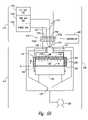
- FIG. 3schematically illustrates a single-wafer ALD reactor 10 having a reaction chamber 20 coupled to a gas supply 30 and a vacuum 40 .
- the reactor 10also includes a workpiece holder 50 that supports the workpiece W and a gas dispenser 60 in the reaction chamber 20 .
- the gas dispenser 60includes a plenum 62 operably coupled to the gas supply 30 and a distributor plate 70 having a plurality of holes 72 .
- the workpiece holder 50heats the workpiece W to a desired temperature
- the gas supply 30selectively injects the first precursor A x , the purge gas, and the second precursor B y , as shown above in FIG. 2 .
- the vacuum 40maintains a negative pressure in the chamber to draw the gases from the gas dispenser 60 across the workpiece W and then through an outlet of the reaction chamber 20 .
- ALD processinghas a relatively low throughput compared to CVD techniques. For example, each A x -purge-B y -purge cycle can take several seconds. This results in a total process time of several minutes to form a 60 ⁇ thick layer. In contrast to ALD processing, CVD techniques require only about one minute to form a 60 ⁇ thick layer.
- the low throughput of existing ALD techniqueslimits the utility of the technology in its current state because it may be a bottleneck in the overall manufacturing process.
- Another drawback of existing ALD reactorsis that the purge pulses may not remove all of the A x or B y molecules from the reactor. As a result, during the pulse of the reactive gas B y , remaining molecules of the reactive gas A x within the reactor volume will react with the B y molecules and produce unwanted particles in the chamber. This may cause defects and/or non-uniformities on the workpiece.
- FIGS. 1A and 1Bare schematic cross-sectional views of stages in an atomic layer deposition processing in accordance with the prior art.
- FIG. 2is a graph illustrating a cycle for forming a layer of material using atomic layer deposition in accordance with the prior art.
- FIG. 3is a schematic representation of a deposition system including a reactor for depositing material onto microfeature workpieces in accordance with the prior art.
- FIG. 4Ais a schematic representation of a system having a reactor for depositing material onto microfeature workpieces in accordance with one embodiment of the invention.
- FIG. 4Bis a schematic representation of the system shown in FIG. 4A at a stage of a method for depositing material onto microfeature workpieces in accordance with an embodiment of the invention.
- FIG. 4Cis a schematic representation of the system shown in FIGS. 4A and 4B at a subsequent stage of a method for depositing materials onto microfeature workpieces in accordance with an embodiment of the invention.
- FIGS. 5A and 5Bare schematic representations of a system having a reactor for depositing a material onto microfeature workpieces in accordance with another embodiment of the invention.
- microfeature workpieceis accordingly used throughout to include substrates upon which and/or in which microelectronic devices, micromechanical devices, storage elements, lenses, optical covers, read/write components, and other features are fabricated.
- microfeature workpiecescan be semiconductor wafers such as silicon or gallium arsenide wafers, glass substrates, insulative substrates, and many other types of materials.
- gasis used throughout to include any form of matter that has no fixed shape and will conform in volume to the space available, which specifically includes vapors (i.e., a gas having a temperature less than the critical temperature so that it may be liquefied or solidified by compression at a constant temperature).
- An embodiment of one such reactorincludes a reaction vessel having a chamber, a workpiece holder in the chamber, and a gas distributor attached to the reaction vessel.
- the workpiece holderincludes a process site aligned with or otherwise superimposed with at least a portion of the gas distributor.
- the process sitehas an outer boundary that defines an area in which a workpiece is placed for processing.
- the gas distributorincludes (a) a first inlet through which reactive gases can flow, (b) a primary dispenser having primary outlets superimposed with the process site and fluidically coupled to the first inlet, and (c) a peripheral dispenser around at least a portion of the primary dispenser.
- the peripheral dispenserhas a second inlet and a perimeter outlet fluidically coupled to the second inlet.
- the perimeter outletis superimposed with a region outside of the outer boundary of the process site so that a non-reactive gas can flow through the perimeter outlet and form a gas curtain around the microfeature workpiece.
- a reactor for depositing thin films on microfeature workpiecesincludes a reaction vessel having a chamber, a gas distributor attached to the reaction vessel, a workpiece holder in the chamber, and a side unit in the reaction vessel at a location relative to the gas distributor and/or the workpiece holder.
- the gas distributorhas an inner compartment including a plurality of primary outlets open to the chamber, and the workpiece holder has a process site aligned with the primary outlets.
- the side unitsurrounds at least a portion of the inner compartment and/or the process site on the workpiece holder.
- the side unitalso has a secondary outlet open to the chamber that operates independently of the primary outlets.
- the inner compartment, the side unit and/or the workpiece holderare movable relative to each other between a first position to form a small-volume cell for introducing the reactant gases to the microfeature workpiece and a second position to form a larger volume space for purging the reactant gases.
- Still another embodiment of a reactor for depositing thin films onto microfeature workpiecesincludes a reaction vessel having a chamber, a gas distributor attached to the vessel, and a workpiece holder in the vessel.
- the gas distributorhas primary outlets configured to direct precursor gases to a desired reaction site, and the workpiece holder is superimposed relative to the gas distributor.
- the gas distributor and/or the workpiece holderare movable with respect to each other to be spaced apart by a first distance during a pulse of precursor gas and a second distance greater than the first distance during a pulse of a purge gas.
- This reactorfurther includes a purge curtain having a secondary outlet aligned with a peripheral region of the workpiece holder to deliver a separate flow of a non-reactive gas around at least a portion of the perimeter of the workpiece.
- a further embodiment of a reactor for depositing thin films on microfeature workpiecescomprises a reaction vessel having a chamber, a workpiece holder in the chamber, a gas distributor attached to the vessel, and a purge curtain having a secondary outlet aligned with a peripheral region of the workpiece holder.
- the workpiece holderhas a process site at which a workpiece is to be located, and the gas distributor has primary outlets configured to direct precursor gases to the process site.
- the gas distributor and/or the workpiece holderare movable with respect to each other.
- This embodiment of a reactorfurther includes a controller having a computer operable medium containing instructions to (a) move the gas distributor and/or the workpiece holder into a first position in which the primary outlets are spaced apart from the workpiece holder by a first distance, (b) deliver a flow of precursor gas through the primary outlets and a flow of purge gas through the secondary outlet while the primary outlets and the workpiece holder are spaced apart by the first distance, (c) move the gas distributor and/or the workpiece holder into a second position in which the primary outlets are spaced apart from the workpiece holder by a second distance greater than the first distance, and (d) deliver a pulse of purge gas while the primary outlets and the workpiece holder are spaced apart by the second distance.
- One aspect of the inventionis directed toward methods for depositing materials onto microfeature workpieces.
- One embodiment of a method for depositing a thin film onto a microfeature workpiececomprises: (a) moving a gas distributor and/or a workpiece holder into a first position in which primary outlets of the gas distributor are spaced apart from the workpiece holder by a first distance; (b) concurrently delivering a flow of precursor gas through the primary outlets and a flow of purge gas through a secondary outlet separate from the primary outlets while the workpiece holder and the primary outlets are spaced apart by the first distance; (c) moving the gas distributor and/or the workpiece holder into a second position in which the primary outlets are spaced apart from the workpiece holder by a second distance greater than the first distance; and (d) dispensing a purge gas onto the workpiece while the primary outlets and the workpiece holder are spaced apart by the second distance.
- Another method of depositing a thin film on a microfeature workpiececomprises: (a) dispensing a flow of a reactant material through primary outlets of a gas distributor and onto a microfeature workpiece; (b) dispensing a first flow of a non-reactant gas through a secondary outlet to flow adjacent to at least a portion of the periphery of the microfeature workpiece while dispensing the flow of the reactant gas through the primary outlets; (c) terminating the flow of the reactant material; and (d) dispensing a second flow of a non-reactant gas onto the microfeature workpiece to purge the reactant gas from the workpiece.
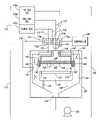
- FIG. 4Ais a schematic representation of a system 100 for depositing a thin film of material onto a microfeature workpiece W in accordance with an embodiment of the invention.
- the system 100includes a reactor 110 and a gas supply 112 operatively coupled to the reactor 110 .
- the reactor 110includes a reaction vessel 120 , a workpiece holder 130 in the reaction vessel 120 , and a gas distributor 140 attached to the reaction vessel 120 .
- the reactor 110also includes a peripheral dispenser 160 that is either a component of the gas distributor 140 or a separate component in the reaction vessel 120 .
- the gas distributor 140 and the peripheral dispenser 160are coupled to various gas sources of the gas supply 112 to provide a peripheral barrier relative to the workpiece W that reduces the volume in which reactant gases are dispensed onto the workpiece W and enhances the separation between individual pulses of reactant gases.
- the reaction vessel 120includes a low pressure chamber 122 defined by interior walls 124 .
- the volume of the chamber 122can be relatively large compared to the size of the workpiece W.
- the reaction vessel 120typically includes an outlet 126 coupled to a vacuum pump 128 for providing a low pressure environment in the chamber 122 .
- the workpiece holder 130is housed within the chamber 122 and has a platform including a process site 132 with an outer boundary 134 that defines an area in which the workpiece W is positioned for processing.
- the workpiece holder 130typically includes a temperature control system that heats or cools the processing site 132 to hold the workpiece W at a desired temperature for the reaction.
- the workpiece holder 130further includes a moveable support 136 (shown schematically) that moves the workpiece holder 130 along a lift path (arrow A) between a first position and a second position.
- the moveable support 136can have guide assembly (e.g., a frame or track) and an actuator (e.g., a servo motor that drives a lead-screw, worm gear, linkage system or other type of device).
- the platformis coupled to the guide assembly and the actuator to raise/lower the platform along the lift path.
- the moveable support 136can have pneumatic or hydraulic cylinders attached to the platform.
- the workpiece holder 130 and/or the gas distributor 140are movable along a lift path between a first position and a second position to adjust the distance between the workpiece holder 130 and the gas distributor 140 .
- the embodiment of the gas distributor 140 shown in FIG. 4Ais at least partially within the reaction vessel 120 and includes a compartment 142 having a distributor plate 144 with a plurality of primary outlets 145 .
- the compartment 142can be attached to the reaction vessel 120 and further include a first inlet 146 for receiving reactant gases and/or non-reactant gases from the gas supply 112 .
- the embodiment of the compartment 142 shown in FIG. 4Adefines an antechamber 148 into which individual reactant gases and/or mixtures of reactant gases are introduced into the reaction vessel 120 . The gases then pass through the primary outlets 145 toward the processing site 132 to interact with the exposed surface of the workpiece W.
- the gas distributor 140can have dedicated lines coupled to one or more of the primary outlets 145 such that individual outlets are dedicated to dispensing a specific type of gas.
- the gas distributor 140can be fixed to the reaction vessel 120 , but in other embodiments the gas distributor 140 can further include an actuator to move the gas distributor along the lift path (arrow A) in addition to or in lieu of moving the workpiece holder 130 .
- the embodiment of the peripheral dispenser 160 illustrated in FIG. 4Ais attached to the gas distributor 140 .
- the peripheral dispenser 160more specifically, is a rim fixed around the periphery of the gas distributor 140 .
- the peripheral dispenser 160further includes a second inlet 161 and a second outlet 162 fluidically coupled to the second inlet 161 .
- the second outlet 162is separate from the first outlet 146 such that the peripheral dispenser 160 can direct a gas flow relative to the workpiece W independently of the gas flow through the primary outlets 145 .
- the peripheral dispenser 160includes a plurality of individual perimeter outlets 162 , but other embodiments of the peripheral dispenser have a single annular second outlet.
- the second outlets 162are superimposed with a region outside of the outer boundary 134 of the process site 132 to provide a gas “curtain” relative to the workpiece W.
- the peripheral dispenser 160is coupled to a source of purge gas to provide a purge curtain relative to the workpiece W.
- the reactor 110operates in conjunction with the gas supply 112 to provide the appropriate sequence of gas pulses for ALD, pulsed CVD or continuous CVD deposition processes.
- the embodiment of the gas supply 112 shown in FIG. 4Aincludes a plurality of gas sources 170 (identified individually as 170 a - c ), a valve assembly 171 having a plurality of valves 172 (identified individually as 172 a - e ), and a plurality of gas lines 173 - 176 .
- the gas sources 170can include a first gas source 170 a for providing a first precursor gas A, a second gas source 170 b for providing a second precursor gas B, and a third gas source 170 c for providing a purge gas P or other type of non-reactive gas.
- the first and second precursors A and Bare generally the constituents that react to form the thin film on the workpiece W.
- the purge gas Pis typically a non-reactive gas compatible with the reaction vessel 120 , the workpiece W, and the first and second precursors A and B.
- the first gas source 170 ais coupled to a first valve 172 b via a line 173
- the second gas source 170 bis coupled to a second valve 172 b via a line 173
- the third gas source 170 cis coupled to (a) a third valve 172 c , (b) a fourth valve 172 d and (c) a fifth valve 172 e by lines 173 .
- the valves 172 a - eare operated by a controller 180 that generates signals for delivering pulses of the individual gases to the reactor 110 via lines 174 , 175 and 176 .
- the controller 180more specifically, operates the valves 172 a - e to pulse the first precursor gas A, the second precursor gas B, and the purge gas P through the primary outlets 145 , the second outlets 162 , and a nozzle 178 at selected stages of a deposition process.
- the pulse widths, flow rates and pulse frequenciesare generally set to accurately control the interaction between the precursor gases A and B in a manner that is expected to improve the quality of the thin film and enhance the throughput of the deposition process.
- the controller 180is generally a computer having a computer operable medium containing instructions to carry out any of the methods described in FIGS. 4B-5B .
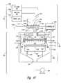
- FIGS. 4B and 4Cillustrate stages of operating the system 100 in accordance with one embodiment of a method of the invention.
- the workpiece holder 130is in a first position P 1 in which the primary outlets 145 of the gas distributor 140 are spaced apart from the workpiece holder 130 by a first distance to define a small volume cavity 400 .
- the controller 180opens the first valve 172 a and the fourth valve 172 d .
- the first precursor gas Aaccordingly flows through the primary outlets 145 and into the small volume cavity 400 , and the purge gas P concurrently flows through the secondary outlet 162 to form a purge curtain (identified by arrows P) around the workpiece W and the workpiece holder 130 .
- This stage of the processaccordingly deposits a layer of molecules of the first precursor gas A onto the workpiece W, and excess molecules of the first precursor A are entrained in the flow of the purge curtain P and directed away from the process site 132 .
- the controller 180then closes valves 172 a and 172 d to terminate the flows of the first precursor gas A and purge gas P.
- FIG. 4Cillustrates a subsequent stage of the method in which the moveable support 136 has moved the workpiece holder 130 into a second position P 2 in which the primary outlets 145 are spaced apart from the workpiece holder 130 by a second distance greater than the first distance.
- the controller 180then opens the third valve 172 c and the fifth valve 172 e so that the purge gas P flows through the primary outlets 145 and the nozzle 178 during a purge cycle.
- the chamber 122is pumped down to a suitable vacuum and the moveable support 136 raises the workpiece holder 130 to the first position P 1 (shown in FIG. 4B ).
- the controllerthen opens the second valve 172 b and the fourth valve 172 d while the workpiece holder is in the first position P 1 .
- the second precursor gas Baccordingly flows through the primary outlets 145 and into the small volume cavity 400 , and the purge gas P flows through the secondary outlet 162 .
- the purge curtaineffectively inhibits remaining molecules of the first precursor A that were not removed from the chamber 122 by the purge cycle from entering the small volume cavity 400 during the pulse of the second precursor B.
- the purge gas Palso carries excess molecules of the second precursor B away from the process site 132 so that errant reactions between the first and second precursors A and B occur away from the workpiece W.
- the controller 180closes the second valve 172 b and the fourth valve 172 d , and the moveable support 136 lowers the workpiece holder 130 to the second position P 2 .
- the purge processis then repeated as described above with reference to FIG. 4C .
- the system 100 illustrated in FIGS. 4A-4Cis expected to increase the throughput of thin film deposition processes.
- the pulse widths of the first and second precursor gases A and Bcan be relatively short because they only need to flow through the small volume cavity 400 instead of the entire chamber 122 .
- Thisnot only reduces the time of the precursor pulses, but it also reduces the excess quantity of precursor molecules that need to be purged from the chamber 122 .
- the pulse width of the purge gasescan also be significantly shorter during the purge cycle compared to conventional processes. This is expected to increase the throughput of vapor deposition processes.
- Another advantage of the embodiment of the system 100 illustrated in FIGS. 4A-4Cis that the purge curtain directs excess molecules of the precursor gases away from the small volume cavity 400 where the ALD half-reactions take place.
- the excess molecules of the precursorsare thus effectively separated from each other and inhibited from collecting on the interior surfaces 124 of the vessel 120 . This is expected to reduce unwanted reactions between the first and second precursors within the reaction vessel 120 , and it is expected to separate any such reactions from the workpiece W.
- the system 100 illustrated above with reference to FIGS. 4A-4Ccan have several different embodiments.
- the gas distributor 140instead of moving the workpiece holder 130 between the first and second positions P 1 and P 2 , the gas distributor 140 can be moved between these positions to form the small volume cavity 400 .
- the system 100can include more than two precursor gases and additional purge gases or other types of non-reactive gases.
- the purge gas Pcan also flow through the secondary outlet 162 during a purge cycle while the workpiece holder is in the second position P 2 .
- the controller 180contains instructions to operate the moveable support 136 in conjunction with the valves 172 a - e.
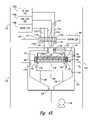
- FIGS. 5A and 5Billustrate a system 500 for depositing a thin film onto microfeature workpieces in accordance with another embodiment of the invention.
- the system 500is similar to the system 100 described above with reference to FIGS. 4A-4C , and thus like reference numbers refer to like components in FIGS. 4A-5B .
- the system 500includes a reactor 510 including the workpiece holder 130 , the gas distributor 140 , and a movable peripheral dispenser 560 .
- the embodiment of the peripheral dispenser 560 shown in FIG. 5Ais movably attached to the gas distributor 140 to move along a lift path A relative to the workpiece holder 130 .
- the peripheral dispenser 560can be attached to the interior surfaces 124 of the reaction vessel 120 instead of the gas distributor 140 .
- the peripheral dispenser 560includes a second outlet 562 aligned with a peripheral region of the workpiece holder 130 .
- the gas supply 512includes the gas sources 170 and a valve assembly 571 having four valves 572 a - d .
- the gas supply 512has four valves instead of five valves as shown in FIGS. 4A-4C because the reactor 510 does not include a side nozzle for the purge gas.
- the peripheral dispenser 560moves downward to a first position P 1 ( FIG. 5B ) to form a small volume cavity 599 having a volume less than the volume of the chamber 122 .
- the controller 180then opens the first valve 172 a and the fourth valve 172 d to flow the first precursor A through the primary outlets 145 and the purge gas through the second outlet 562 .
- the peripheral dispenser 560then moves to a second position P 2 ( FIG. 5A ), and the controller 180 operates the valve assembly 571 so that the purge gas flows through the first outlets 145 and/or the second outlet 162 to purge excess molecules of the precursor gases from the chamber 122 .
- the peripheral dispensercan be a side unit that is fixed to or moveably carried by (a) the gas distributor, (b) the workpiece support, and/or (c) the reaction vessel. Accordingly, the invention is not limited except as by the appended claims.
Landscapes
- Chemical & Material Sciences (AREA)
- General Chemical & Material Sciences (AREA)
- Chemical Kinetics & Catalysis (AREA)
- Engineering & Computer Science (AREA)
- Materials Engineering (AREA)
- Mechanical Engineering (AREA)
- Metallurgy (AREA)
- Organic Chemistry (AREA)
- Chemical Vapour Deposition (AREA)
Abstract
Description
Claims (16)
Priority Applications (1)
| Application Number | Priority Date | Filing Date | Title |
|---|---|---|---|
| US10/859,883US7699932B2 (en) | 2004-06-02 | 2004-06-02 | Reactors, systems and methods for depositing thin films onto microfeature workpieces |
Applications Claiming Priority (1)
| Application Number | Priority Date | Filing Date | Title |
|---|---|---|---|
| US10/859,883US7699932B2 (en) | 2004-06-02 | 2004-06-02 | Reactors, systems and methods for depositing thin films onto microfeature workpieces |
Publications (2)
| Publication Number | Publication Date |
|---|---|
| US20050268856A1 US20050268856A1 (en) | 2005-12-08 |
| US7699932B2true US7699932B2 (en) | 2010-04-20 |
Family
ID=35446300
Family Applications (1)
| Application Number | Title | Priority Date | Filing Date |
|---|---|---|---|
| US10/859,883Active2026-04-07US7699932B2 (en) | 2004-06-02 | 2004-06-02 | Reactors, systems and methods for depositing thin films onto microfeature workpieces |
Country Status (1)
| Country | Link |
|---|---|
| US (1) | US7699932B2 (en) |
Cited By (21)
| Publication number | Priority date | Publication date | Assignee | Title |
|---|---|---|---|---|
| US20070044716A1 (en)* | 2005-08-24 | 2007-03-01 | Tsutomu Tetsuka | Plasma processing apparatus |
| US20090078677A1 (en)* | 2007-06-29 | 2009-03-26 | Neil Benjamin | Integrated steerability array arrangement for minimizing non-uniformity |
| US20090236447A1 (en)* | 2008-03-21 | 2009-09-24 | Applied Materials, Inc. | Method and apparatus for controlling gas injection in process chamber |
| US20120000542A1 (en)* | 2010-06-30 | 2012-01-05 | Kabushiki Kaisha Toshiba | Mass flow controller, mass flow controller system, substrate processing device, and gas flow rate adjusting method |
| US20120059502A1 (en)* | 2010-09-07 | 2012-03-08 | Tokyo Electron Limited | Substrate transfer method and storage medium |
| US20120160173A1 (en)* | 2010-12-23 | 2012-06-28 | Richard Endo | Vapor Based Processing System with Purge Mode |
| US20120180725A1 (en)* | 2011-01-17 | 2012-07-19 | Furukawa Electric Co., Ltd. | Cvd apparatus |
| US20120266821A1 (en)* | 2005-01-18 | 2012-10-25 | Asm America, Inc. | Reaction system for growing a thin film |
| US20130014895A1 (en)* | 2011-07-08 | 2013-01-17 | Tokyo Electron Limited | Substrate processing apparatus |
| US20130266728A1 (en)* | 2012-04-06 | 2013-10-10 | Samsung Display Co., Ltd. | Thin film depositing apparatus and thin film depositing method using the same |
| US8668778B2 (en) | 2006-07-07 | 2014-03-11 | Tel Fsi, Inc. | Method of removing liquid from a barrier structure |
| US8684015B2 (en) | 2008-05-09 | 2014-04-01 | Tel Fsi, Inc. | Tools and methods for processing microelectronic workpieces using process chamber designs that easily transition between open and closed modes of operation |
| US20150329967A1 (en)* | 2010-08-27 | 2015-11-19 | Nuflare Technology, Inc. | Film-forming manufacturing apparatus and method |
| US9490149B2 (en) | 2013-07-03 | 2016-11-08 | Lam Research Corporation | Chemical deposition apparatus having conductance control |
| US10119608B2 (en)* | 2015-03-02 | 2018-11-06 | Nsk Ltd. | Grease application method, application device, and methods for manufacturing worm-type reducer, electric power steering device, automobile and variety of industrial machines |
| US10358721B2 (en)* | 2015-10-22 | 2019-07-23 | Asm Ip Holding B.V. | Semiconductor manufacturing system including deposition apparatus |
| US10403515B2 (en)* | 2015-09-24 | 2019-09-03 | Applied Materials, Inc. | Loadlock integrated bevel etcher system |
| US10526700B2 (en)* | 2014-12-19 | 2020-01-07 | Lam Research Corporation | Hardware and process for film uniformity improvement |
| US10781516B2 (en) | 2013-06-28 | 2020-09-22 | Lam Research Corporation | Chemical deposition chamber having gas seal |
| US10954594B2 (en)* | 2015-09-30 | 2021-03-23 | Applied Materials, Inc. | High temperature vapor delivery system and method |
| US20220037577A1 (en)* | 2019-02-25 | 2022-02-03 | Corning Incorporated | Multi-showerhead chemical vapor deposition reactor, process and products |
Families Citing this family (376)
| Publication number | Priority date | Publication date | Assignee | Title |
|---|---|---|---|---|
| US6838114B2 (en) | 2002-05-24 | 2005-01-04 | Micron Technology, Inc. | Methods for controlling gas pulsing in processes for depositing materials onto micro-device workpieces |
| US6821347B2 (en) | 2002-07-08 | 2004-11-23 | Micron Technology, Inc. | Apparatus and method for depositing materials onto microelectronic workpieces |
| US6955725B2 (en) | 2002-08-15 | 2005-10-18 | Micron Technology, Inc. | Reactors with isolated gas connectors and methods for depositing materials onto micro-device workpieces |
| US6926775B2 (en) | 2003-02-11 | 2005-08-09 | Micron Technology, Inc. | Reactors with isolated gas connectors and methods for depositing materials onto micro-device workpieces |
| US7422635B2 (en) | 2003-08-28 | 2008-09-09 | Micron Technology, Inc. | Methods and apparatus for processing microfeature workpieces, e.g., for depositing materials on microfeature workpieces |
| US7056806B2 (en) | 2003-09-17 | 2006-06-06 | Micron Technology, Inc. | Microfeature workpiece processing apparatus and methods for controlling deposition of materials on microfeature workpieces |
| US7258892B2 (en) | 2003-12-10 | 2007-08-21 | Micron Technology, Inc. | Methods and systems for controlling temperature during microfeature workpiece processing, e.g., CVD deposition |
| US7906393B2 (en) | 2004-01-28 | 2011-03-15 | Micron Technology, Inc. | Methods for forming small-scale capacitor structures |
| US7700155B1 (en)* | 2004-04-08 | 2010-04-20 | Novellus Systems, Inc. | Method and apparatus for modulation of precursor exposure during a pulsed deposition process |
| US8133554B2 (en) | 2004-05-06 | 2012-03-13 | Micron Technology, Inc. | Methods for depositing material onto microfeature workpieces in reaction chambers and systems for depositing materials onto microfeature workpieces |
| US7699932B2 (en)* | 2004-06-02 | 2010-04-20 | Micron Technology, Inc. | Reactors, systems and methods for depositing thin films onto microfeature workpieces |
| US7681581B2 (en) | 2005-04-01 | 2010-03-23 | Fsi International, Inc. | Compact duct system incorporating moveable and nestable baffles for use in tools used to process microelectronic workpieces with one or more treatment fluids |
| US8815014B2 (en)* | 2005-11-18 | 2014-08-26 | Tokyo Electron Limited | Method and system for performing different deposition processes within a single chamber |
| JP5347294B2 (en)* | 2007-09-12 | 2013-11-20 | 東京エレクトロン株式会社 | Film forming apparatus, film forming method, and storage medium |
| US8721836B2 (en) | 2008-04-22 | 2014-05-13 | Micron Technology, Inc. | Plasma processing with preionized and predissociated tuning gases and associated systems and methods |
| US8216380B2 (en)* | 2009-01-08 | 2012-07-10 | Asm America, Inc. | Gap maintenance for opening to process chamber |
| US8287648B2 (en)* | 2009-02-09 | 2012-10-16 | Asm America, Inc. | Method and apparatus for minimizing contamination in semiconductor processing chamber |
| US9394608B2 (en) | 2009-04-06 | 2016-07-19 | Asm America, Inc. | Semiconductor processing reactor and components thereof |
| US8802201B2 (en) | 2009-08-14 | 2014-08-12 | Asm America, Inc. | Systems and methods for thin-film deposition of metal oxides using excited nitrogen-oxygen species |
| FI20105903A0 (en)* | 2010-08-30 | 2010-08-30 | Beneq Oy | Device |
| US9695510B2 (en)* | 2011-04-21 | 2017-07-04 | Kurt J. Lesker Company | Atomic layer deposition apparatus and process |
| US9175392B2 (en)* | 2011-06-17 | 2015-11-03 | Intermolecular, Inc. | System for multi-region processing |
| US20130023129A1 (en) | 2011-07-20 | 2013-01-24 | Asm America, Inc. | Pressure transmitter for a semiconductor processing environment |
| US9017481B1 (en) | 2011-10-28 | 2015-04-28 | Asm America, Inc. | Process feed management for semiconductor substrate processing |
| US9083182B2 (en) | 2011-11-21 | 2015-07-14 | Lam Research Corporation | Bypass capacitors for high voltage bias power in the mid frequency RF range |
| US10586686B2 (en) | 2011-11-22 | 2020-03-10 | Law Research Corporation | Peripheral RF feed and symmetric RF return for symmetric RF delivery |
| US9396908B2 (en) | 2011-11-22 | 2016-07-19 | Lam Research Corporation | Systems and methods for controlling a plasma edge region |
| US9263240B2 (en) | 2011-11-22 | 2016-02-16 | Lam Research Corporation | Dual zone temperature control of upper electrodes |
| KR101971312B1 (en)* | 2011-11-23 | 2019-04-22 | 램 리써치 코포레이션 | Multi zone gas injection upper electrode system |
| WO2013078434A1 (en) | 2011-11-24 | 2013-05-30 | Lam Research Corporation | Plasma processing chamber with flexible symmetric rf return strap |
| US9388494B2 (en) | 2012-06-25 | 2016-07-12 | Novellus Systems, Inc. | Suppression of parasitic deposition in a substrate processing system by suppressing precursor flow and plasma outside of substrate region |
| FI125341B (en)* | 2012-07-09 | 2015-08-31 | Beneq Oy | Apparatus and method for processing substrates |
| US10486183B2 (en)* | 2012-07-27 | 2019-11-26 | Applied Materials, Inc. | Methods and apparatus for delivering process gases to a substrate |
| US9132436B2 (en) | 2012-09-21 | 2015-09-15 | Applied Materials, Inc. | Chemical control features in wafer process equipment |
| US10714315B2 (en) | 2012-10-12 | 2020-07-14 | Asm Ip Holdings B.V. | Semiconductor reaction chamber showerhead |
| TWI480417B (en) | 2012-11-02 | 2015-04-11 | Ind Tech Res Inst | Air showr device having air curtain and apparatus for depositing film using the same |
| US20160376700A1 (en) | 2013-02-01 | 2016-12-29 | Asm Ip Holding B.V. | System for treatment of deposition reactor |
| US10256079B2 (en) | 2013-02-08 | 2019-04-09 | Applied Materials, Inc. | Semiconductor processing systems having multiple plasma configurations |
| US11414759B2 (en)* | 2013-11-29 | 2022-08-16 | Taiwan Semiconductor Manufacturing Co., Ltd | Mechanisms for supplying process gas into wafer process apparatus |
| CN106415876B (en) | 2014-01-21 | 2018-06-26 | 应用材料公司 | Allow the thin-film package processing system and process kit that low-pressure tool is replaced |
| US11015245B2 (en) | 2014-03-19 | 2021-05-25 | Asm Ip Holding B.V. | Gas-phase reactor and system having exhaust plenum and components thereof |
| JP6225837B2 (en)* | 2014-06-04 | 2017-11-08 | 東京エレクトロン株式会社 | Film forming apparatus, film forming method, storage medium |
| JP6225842B2 (en)* | 2014-06-16 | 2017-11-08 | 東京エレクトロン株式会社 | Film forming apparatus, film forming method, storage medium |
| US10858737B2 (en) | 2014-07-28 | 2020-12-08 | Asm Ip Holding B.V. | Showerhead assembly and components thereof |
| JP2016036018A (en)* | 2014-07-31 | 2016-03-17 | 東京エレクトロン株式会社 | Plasma processing device and gas supply member |
| US9890456B2 (en) | 2014-08-21 | 2018-02-13 | Asm Ip Holding B.V. | Method and system for in situ formation of gas-phase compounds |
| US20160068961A1 (en)* | 2014-09-05 | 2016-03-10 | Aixtron Se | Method and Apparatus For Growing Binary, Ternary and Quaternary Materials on a Substrate |
| US10941490B2 (en) | 2014-10-07 | 2021-03-09 | Asm Ip Holding B.V. | Multiple temperature range susceptor, assembly, reactor and system including the susceptor, and methods of using the same |
| JP6516436B2 (en)* | 2014-10-24 | 2019-05-22 | 東京エレクトロン株式会社 | Film forming apparatus and film forming method |
| JP6354539B2 (en)* | 2014-11-25 | 2018-07-11 | 東京エレクトロン株式会社 | Substrate processing apparatus, substrate processing method, and storage medium |
| US11637002B2 (en) | 2014-11-26 | 2023-04-25 | Applied Materials, Inc. | Methods and systems to enhance process uniformity |
| US20160225652A1 (en) | 2015-02-03 | 2016-08-04 | Applied Materials, Inc. | Low temperature chuck for plasma processing systems |
| US10276355B2 (en) | 2015-03-12 | 2019-04-30 | Asm Ip Holding B.V. | Multi-zone reactor, system including the reactor, and method of using the same |
| US10253412B2 (en)* | 2015-05-22 | 2019-04-09 | Lam Research Corporation | Deposition apparatus including edge plenum showerhead assembly |
| US10023959B2 (en) | 2015-05-26 | 2018-07-17 | Lam Research Corporation | Anti-transient showerhead |
| US10458018B2 (en) | 2015-06-26 | 2019-10-29 | Asm Ip Holding B.V. | Structures including metal carbide material, devices including the structures, and methods of forming same |
| US9741593B2 (en) | 2015-08-06 | 2017-08-22 | Applied Materials, Inc. | Thermal management systems and methods for wafer processing systems |
| US10504700B2 (en) | 2015-08-27 | 2019-12-10 | Applied Materials, Inc. | Plasma etching systems and methods with secondary plasma injection |
| US10211308B2 (en) | 2015-10-21 | 2019-02-19 | Asm Ip Holding B.V. | NbMC layers |
| US11139308B2 (en) | 2015-12-29 | 2021-10-05 | Asm Ip Holding B.V. | Atomic layer deposition of III-V compounds to form V-NAND devices |
| US9953843B2 (en) | 2016-02-05 | 2018-04-24 | Lam Research Corporation | Chamber for patterning non-volatile metals |
| US10529554B2 (en) | 2016-02-19 | 2020-01-07 | Asm Ip Holding B.V. | Method for forming silicon nitride film selectively on sidewalls or flat surfaces of trenches |
| US10343920B2 (en) | 2016-03-18 | 2019-07-09 | Asm Ip Holding B.V. | Aligned carbon nanotubes |
| US10865475B2 (en) | 2016-04-21 | 2020-12-15 | Asm Ip Holding B.V. | Deposition of metal borides and silicides |
| US10190213B2 (en) | 2016-04-21 | 2019-01-29 | Asm Ip Holding B.V. | Deposition of metal borides |
| US10367080B2 (en) | 2016-05-02 | 2019-07-30 | Asm Ip Holding B.V. | Method of forming a germanium oxynitride film |
| US10504754B2 (en) | 2016-05-19 | 2019-12-10 | Applied Materials, Inc. | Systems and methods for improved semiconductor etching and component protection |
| US11453943B2 (en) | 2016-05-25 | 2022-09-27 | Asm Ip Holding B.V. | Method for forming carbon-containing silicon/metal oxide or nitride film by ALD using silicon precursor and hydrocarbon precursor |
| US9738977B1 (en)* | 2016-06-17 | 2017-08-22 | Lam Research Corporation | Showerhead curtain gas method and system for film profile modulation |
| US9865484B1 (en) | 2016-06-29 | 2018-01-09 | Applied Materials, Inc. | Selective etch using material modification and RF pulsing |
| US9859151B1 (en) | 2016-07-08 | 2018-01-02 | Asm Ip Holding B.V. | Selective film deposition method to form air gaps |
| US10612137B2 (en) | 2016-07-08 | 2020-04-07 | Asm Ip Holdings B.V. | Organic reactants for atomic layer deposition |
| US9812320B1 (en) | 2016-07-28 | 2017-11-07 | Asm Ip Holding B.V. | Method and apparatus for filling a gap |
| US9887082B1 (en) | 2016-07-28 | 2018-02-06 | Asm Ip Holding B.V. | Method and apparatus for filling a gap |
| KR102532607B1 (en) | 2016-07-28 | 2023-05-15 | 에이에스엠 아이피 홀딩 비.브이. | Substrate processing apparatus and method of operating the same |
| US10546729B2 (en)* | 2016-10-04 | 2020-01-28 | Applied Materials, Inc. | Dual-channel showerhead with improved profile |
| US10643826B2 (en) | 2016-10-26 | 2020-05-05 | Asm Ip Holdings B.V. | Methods for thermally calibrating reaction chambers |
| US11532757B2 (en) | 2016-10-27 | 2022-12-20 | Asm Ip Holding B.V. | Deposition of charge trapping layers |
| US10229833B2 (en) | 2016-11-01 | 2019-03-12 | Asm Ip Holding B.V. | Methods for forming a transition metal nitride film on a substrate by atomic layer deposition and related semiconductor device structures |
| US10714350B2 (en) | 2016-11-01 | 2020-07-14 | ASM IP Holdings, B.V. | Methods for forming a transition metal niobium nitride film on a substrate by atomic layer deposition and related semiconductor device structures |
| KR102546317B1 (en) | 2016-11-15 | 2023-06-21 | 에이에스엠 아이피 홀딩 비.브이. | Gas supply unit and substrate processing apparatus including the same |
| KR102762543B1 (en) | 2016-12-14 | 2025-02-05 | 에이에스엠 아이피 홀딩 비.브이. | Substrate processing apparatus |
| US11581186B2 (en) | 2016-12-15 | 2023-02-14 | Asm Ip Holding B.V. | Sequential infiltration synthesis apparatus |
| US11447861B2 (en) | 2016-12-15 | 2022-09-20 | Asm Ip Holding B.V. | Sequential infiltration synthesis apparatus and a method of forming a patterned structure |
| KR102700194B1 (en)* | 2016-12-19 | 2024-08-28 | 에이에스엠 아이피 홀딩 비.브이. | Substrate processing apparatus |
| US10269558B2 (en) | 2016-12-22 | 2019-04-23 | Asm Ip Holding B.V. | Method of forming a structure on a substrate |
| US10867788B2 (en) | 2016-12-28 | 2020-12-15 | Asm Ip Holding B.V. | Method of forming a structure on a substrate |
| US11390950B2 (en) | 2017-01-10 | 2022-07-19 | Asm Ip Holding B.V. | Reactor system and method to reduce residue buildup during a film deposition process |
| US10431429B2 (en) | 2017-02-03 | 2019-10-01 | Applied Materials, Inc. | Systems and methods for radial and azimuthal control of plasma uniformity |
| US10468261B2 (en) | 2017-02-15 | 2019-11-05 | Asm Ip Holding B.V. | Methods for forming a metallic film on a substrate by cyclical deposition and related semiconductor device structures |
| US10943834B2 (en) | 2017-03-13 | 2021-03-09 | Applied Materials, Inc. | Replacement contact process |
| US10529563B2 (en) | 2017-03-29 | 2020-01-07 | Asm Ip Holdings B.V. | Method for forming doped metal oxide films on a substrate by cyclical deposition and related semiconductor device structures |
| KR102457289B1 (en) | 2017-04-25 | 2022-10-21 | 에이에스엠 아이피 홀딩 비.브이. | Method for depositing a thin film and manufacturing a semiconductor device |
| US10892156B2 (en) | 2017-05-08 | 2021-01-12 | Asm Ip Holding B.V. | Methods for forming a silicon nitride film on a substrate and related semiconductor device structures |
| US10770286B2 (en) | 2017-05-08 | 2020-09-08 | Asm Ip Holdings B.V. | Methods for selectively forming a silicon nitride film on a substrate and related semiconductor device structures |
| US11276590B2 (en) | 2017-05-17 | 2022-03-15 | Applied Materials, Inc. | Multi-zone semiconductor substrate supports |
| JP7176860B6 (en) | 2017-05-17 | 2022-12-16 | アプライド マテリアルズ インコーポレイテッド | Semiconductor processing chamber to improve precursor flow |
| US11276559B2 (en) | 2017-05-17 | 2022-03-15 | Applied Materials, Inc. | Semiconductor processing chamber for multiple precursor flow |
| US10886123B2 (en) | 2017-06-02 | 2021-01-05 | Asm Ip Holding B.V. | Methods for forming low temperature semiconductor layers and related semiconductor device structures |
| US12040200B2 (en) | 2017-06-20 | 2024-07-16 | Asm Ip Holding B.V. | Semiconductor processing apparatus and methods for calibrating a semiconductor processing apparatus |
| US11306395B2 (en) | 2017-06-28 | 2022-04-19 | Asm Ip Holding B.V. | Methods for depositing a transition metal nitride film on a substrate by atomic layer deposition and related deposition apparatus |
| KR20190009245A (en) | 2017-07-18 | 2019-01-28 | 에이에스엠 아이피 홀딩 비.브이. | Methods for forming a semiconductor device structure and related semiconductor device structures |
| US10541333B2 (en) | 2017-07-19 | 2020-01-21 | Asm Ip Holding B.V. | Method for depositing a group IV semiconductor and related semiconductor device structures |
| US11018002B2 (en) | 2017-07-19 | 2021-05-25 | Asm Ip Holding B.V. | Method for selectively depositing a Group IV semiconductor and related semiconductor device structures |
| US11374112B2 (en) | 2017-07-19 | 2022-06-28 | Asm Ip Holding B.V. | Method for depositing a group IV semiconductor and related semiconductor device structures |
| US10590535B2 (en) | 2017-07-26 | 2020-03-17 | Asm Ip Holdings B.V. | Chemical treatment, deposition and/or infiltration apparatus and method for using the same |
| TWI815813B (en) | 2017-08-04 | 2023-09-21 | 荷蘭商Asm智慧財產控股公司 | Showerhead assembly for distributing a gas within a reaction chamber |
| US10297458B2 (en) | 2017-08-07 | 2019-05-21 | Applied Materials, Inc. | Process window widening using coated parts in plasma etch processes |
| US10770336B2 (en) | 2017-08-08 | 2020-09-08 | Asm Ip Holding B.V. | Substrate lift mechanism and reactor including same |
| US10692741B2 (en) | 2017-08-08 | 2020-06-23 | Asm Ip Holdings B.V. | Radiation shield |
| US11139191B2 (en) | 2017-08-09 | 2021-10-05 | Asm Ip Holding B.V. | Storage apparatus for storing cassettes for substrates and processing apparatus equipped therewith |
| US11769682B2 (en) | 2017-08-09 | 2023-09-26 | Asm Ip Holding B.V. | Storage apparatus for storing cassettes for substrates and processing apparatus equipped therewith |
| US11830730B2 (en) | 2017-08-29 | 2023-11-28 | Asm Ip Holding B.V. | Layer forming method and apparatus |
| KR102491945B1 (en) | 2017-08-30 | 2023-01-26 | 에이에스엠 아이피 홀딩 비.브이. | Substrate processing apparatus |
| US11056344B2 (en) | 2017-08-30 | 2021-07-06 | Asm Ip Holding B.V. | Layer forming method |
| US11295980B2 (en) | 2017-08-30 | 2022-04-05 | Asm Ip Holding B.V. | Methods for depositing a molybdenum metal film over a dielectric surface of a substrate by a cyclical deposition process and related semiconductor device structures |
| KR102401446B1 (en) | 2017-08-31 | 2022-05-24 | 에이에스엠 아이피 홀딩 비.브이. | Substrate processing apparatus |
| KR102630301B1 (en) | 2017-09-21 | 2024-01-29 | 에이에스엠 아이피 홀딩 비.브이. | Method of sequential infiltration synthesis treatment of infiltrateable material and structures and devices formed using same |
| US10844484B2 (en) | 2017-09-22 | 2020-11-24 | Asm Ip Holding B.V. | Apparatus for dispensing a vapor phase reactant to a reaction chamber and related methods |
| US10658205B2 (en) | 2017-09-28 | 2020-05-19 | Asm Ip Holdings B.V. | Chemical dispensing apparatus and methods for dispensing a chemical to a reaction chamber |
| US10403504B2 (en) | 2017-10-05 | 2019-09-03 | Asm Ip Holding B.V. | Method for selectively depositing a metallic film on a substrate |
| US10923344B2 (en) | 2017-10-30 | 2021-02-16 | Asm Ip Holding B.V. | Methods for forming a semiconductor structure and related semiconductor structures |
| US10872804B2 (en) | 2017-11-03 | 2020-12-22 | Asm Ip Holding B.V. | Apparatus and methods for isolating a reaction chamber from a loading chamber resulting in reduced contamination |
| US10872803B2 (en) | 2017-11-03 | 2020-12-22 | Asm Ip Holding B.V. | Apparatus and methods for isolating a reaction chamber from a loading chamber resulting in reduced contamination |
| US10910262B2 (en) | 2017-11-16 | 2021-02-02 | Asm Ip Holding B.V. | Method of selectively depositing a capping layer structure on a semiconductor device structure |
| US11022879B2 (en) | 2017-11-24 | 2021-06-01 | Asm Ip Holding B.V. | Method of forming an enhanced unexposed photoresist layer |
| CN111344522B (en) | 2017-11-27 | 2022-04-12 | 阿斯莫Ip控股公司 | Including clean mini-environment device |
| WO2019103613A1 (en) | 2017-11-27 | 2019-05-31 | Asm Ip Holding B.V. | A storage device for storing wafer cassettes for use with a batch furnace |
| US10903054B2 (en) | 2017-12-19 | 2021-01-26 | Applied Materials, Inc. | Multi-zone gas distribution systems and methods |
| US11328909B2 (en) | 2017-12-22 | 2022-05-10 | Applied Materials, Inc. | Chamber conditioning and removal processes |
| US10854426B2 (en) | 2018-01-08 | 2020-12-01 | Applied Materials, Inc. | Metal recess for semiconductor structures |
| US10872771B2 (en) | 2018-01-16 | 2020-12-22 | Asm Ip Holding B. V. | Method for depositing a material film on a substrate within a reaction chamber by a cyclical deposition process and related device structures |
| KR102695659B1 (en) | 2018-01-19 | 2024-08-14 | 에이에스엠 아이피 홀딩 비.브이. | Method for depositing a gap filling layer by plasma assisted deposition |
| TWI799494B (en) | 2018-01-19 | 2023-04-21 | 荷蘭商Asm 智慧財產控股公司 | Deposition method |
| US11018047B2 (en) | 2018-01-25 | 2021-05-25 | Asm Ip Holding B.V. | Hybrid lift pin |
| USD880437S1 (en) | 2018-02-01 | 2020-04-07 | Asm Ip Holding B.V. | Gas supply plate for semiconductor manufacturing apparatus |
| US11081345B2 (en) | 2018-02-06 | 2021-08-03 | Asm Ip Holding B.V. | Method of post-deposition treatment for silicon oxide film |
| WO2019158960A1 (en) | 2018-02-14 | 2019-08-22 | Asm Ip Holding B.V. | A method for depositing a ruthenium-containing film on a substrate by a cyclical deposition process |
| US10896820B2 (en) | 2018-02-14 | 2021-01-19 | Asm Ip Holding B.V. | Method for depositing a ruthenium-containing film on a substrate by a cyclical deposition process |
| US10964512B2 (en) | 2018-02-15 | 2021-03-30 | Applied Materials, Inc. | Semiconductor processing chamber multistage mixing apparatus and methods |
| US10731249B2 (en) | 2018-02-15 | 2020-08-04 | Asm Ip Holding B.V. | Method of forming a transition metal containing film on a substrate by a cyclical deposition process, a method for supplying a transition metal halide compound to a reaction chamber, and related vapor deposition apparatus |
| KR102636427B1 (en) | 2018-02-20 | 2024-02-13 | 에이에스엠 아이피 홀딩 비.브이. | Substrate processing method and apparatus |
| US10975470B2 (en) | 2018-02-23 | 2021-04-13 | Asm Ip Holding B.V. | Apparatus for detecting or monitoring for a chemical precursor in a high temperature environment |
| US11473195B2 (en) | 2018-03-01 | 2022-10-18 | Asm Ip Holding B.V. | Semiconductor processing apparatus and a method for processing a substrate |
| US11629406B2 (en) | 2018-03-09 | 2023-04-18 | Asm Ip Holding B.V. | Semiconductor processing apparatus comprising one or more pyrometers for measuring a temperature of a substrate during transfer of the substrate |
| US10319600B1 (en) | 2018-03-12 | 2019-06-11 | Applied Materials, Inc. | Thermal silicon etch |
| US11114283B2 (en) | 2018-03-16 | 2021-09-07 | Asm Ip Holding B.V. | Reactor, system including the reactor, and methods of manufacturing and using same |
| KR102646467B1 (en) | 2018-03-27 | 2024-03-11 | 에이에스엠 아이피 홀딩 비.브이. | Method of forming an electrode on a substrate and a semiconductor device structure including an electrode |
| US11088002B2 (en) | 2018-03-29 | 2021-08-10 | Asm Ip Holding B.V. | Substrate rack and a substrate processing system and method |
| US11230766B2 (en) | 2018-03-29 | 2022-01-25 | Asm Ip Holding B.V. | Substrate processing apparatus and method |
| KR102501472B1 (en) | 2018-03-30 | 2023-02-20 | 에이에스엠 아이피 홀딩 비.브이. | Substrate processing method |
| KR102600229B1 (en) | 2018-04-09 | 2023-11-10 | 에이에스엠 아이피 홀딩 비.브이. | Substrate supporting device, substrate processing apparatus including the same and substrate processing method |
| US10886137B2 (en) | 2018-04-30 | 2021-01-05 | Applied Materials, Inc. | Selective nitride removal |
| US12025484B2 (en) | 2018-05-08 | 2024-07-02 | Asm Ip Holding B.V. | Thin film forming method |
| TWI811348B (en) | 2018-05-08 | 2023-08-11 | 荷蘭商Asm 智慧財產控股公司 | Methods for depositing an oxide film on a substrate by a cyclical deposition process and related device structures |
| US12272527B2 (en) | 2018-05-09 | 2025-04-08 | Asm Ip Holding B.V. | Apparatus for use with hydrogen radicals and method of using same |
| KR20190129718A (en) | 2018-05-11 | 2019-11-20 | 에이에스엠 아이피 홀딩 비.브이. | Methods for forming a doped metal carbide film on a substrate and related semiconductor device structures |
| US12012652B2 (en)* | 2018-05-21 | 2024-06-18 | Applied Materials, Inc. | Single process volume to perform high-pressure and low-pressure processes with features to reduce cross-contamination |
| KR102596988B1 (en) | 2018-05-28 | 2023-10-31 | 에이에스엠 아이피 홀딩 비.브이. | Method of processing a substrate and a device manufactured by the same |
| TWI840362B (en) | 2018-06-04 | 2024-05-01 | 荷蘭商Asm Ip私人控股有限公司 | Wafer handling chamber with moisture reduction |
| US11718913B2 (en) | 2018-06-04 | 2023-08-08 | Asm Ip Holding B.V. | Gas distribution system and reactor system including same |
| US11286562B2 (en) | 2018-06-08 | 2022-03-29 | Asm Ip Holding B.V. | Gas-phase chemical reactor and method of using same |
| US10797133B2 (en) | 2018-06-21 | 2020-10-06 | Asm Ip Holding B.V. | Method for depositing a phosphorus doped silicon arsenide film and related semiconductor device structures |
| KR102568797B1 (en) | 2018-06-21 | 2023-08-21 | 에이에스엠 아이피 홀딩 비.브이. | Substrate processing system |
| KR102854019B1 (en) | 2018-06-27 | 2025-09-02 | 에이에스엠 아이피 홀딩 비.브이. | Periodic deposition method for forming a metal-containing material and films and structures comprising the metal-containing material |
| TWI873894B (en) | 2018-06-27 | 2025-02-21 | 荷蘭商Asm Ip私人控股有限公司 | Cyclic deposition methods for forming metal-containing material and films and structures including the metal-containing material |
| KR102686758B1 (en) | 2018-06-29 | 2024-07-18 | 에이에스엠 아이피 홀딩 비.브이. | Method for depositing a thin film and manufacturing a semiconductor device |
| US10612136B2 (en) | 2018-06-29 | 2020-04-07 | ASM IP Holding, B.V. | Temperature-controlled flange and reactor system including same |
| US10388513B1 (en) | 2018-07-03 | 2019-08-20 | Asm Ip Holding B.V. | Method for depositing silicon-free carbon-containing film as gap-fill layer by pulse plasma-assisted deposition |
| US10755922B2 (en) | 2018-07-03 | 2020-08-25 | Asm Ip Holding B.V. | Method for depositing silicon-free carbon-containing film as gap-fill layer by pulse plasma-assisted deposition |
| US10767789B2 (en) | 2018-07-16 | 2020-09-08 | Asm Ip Holding B.V. | Diaphragm valves, valve components, and methods for forming valve components |
| US11053591B2 (en) | 2018-08-06 | 2021-07-06 | Asm Ip Holding B.V. | Multi-port gas injection system and reactor system including same |
| US10883175B2 (en) | 2018-08-09 | 2021-01-05 | Asm Ip Holding B.V. | Vertical furnace for processing substrates and a liner for use therein |
| US10829852B2 (en) | 2018-08-16 | 2020-11-10 | Asm Ip Holding B.V. | Gas distribution device for a wafer processing apparatus |
| US11430674B2 (en) | 2018-08-22 | 2022-08-30 | Asm Ip Holding B.V. | Sensor array, apparatus for dispensing a vapor phase reactant to a reaction chamber and related methods |
| KR102707956B1 (en) | 2018-09-11 | 2024-09-19 | 에이에스엠 아이피 홀딩 비.브이. | Method for deposition of a thin film |
| US11024523B2 (en) | 2018-09-11 | 2021-06-01 | Asm Ip Holding B.V. | Substrate processing apparatus and method |
| US11049751B2 (en) | 2018-09-14 | 2021-06-29 | Asm Ip Holding B.V. | Cassette supply system to store and handle cassettes and processing apparatus equipped therewith |
| US11049755B2 (en) | 2018-09-14 | 2021-06-29 | Applied Materials, Inc. | Semiconductor substrate supports with embedded RF shield |
| US10892198B2 (en) | 2018-09-14 | 2021-01-12 | Applied Materials, Inc. | Systems and methods for improved performance in semiconductor processing |
| US11062887B2 (en) | 2018-09-17 | 2021-07-13 | Applied Materials, Inc. | High temperature RF heater pedestals |
| US11417534B2 (en) | 2018-09-21 | 2022-08-16 | Applied Materials, Inc. | Selective material removal |
| CN110970344B (en) | 2018-10-01 | 2024-10-25 | Asmip控股有限公司 | Substrate holding apparatus, system comprising the same and method of using the same |
| US11232963B2 (en) | 2018-10-03 | 2022-01-25 | Asm Ip Holding B.V. | Substrate processing apparatus and method |
| KR102592699B1 (en) | 2018-10-08 | 2023-10-23 | 에이에스엠 아이피 홀딩 비.브이. | Substrate support unit and apparatuses for depositing thin film and processing the substrate including the same |
| US11682560B2 (en) | 2018-10-11 | 2023-06-20 | Applied Materials, Inc. | Systems and methods for hafnium-containing film removal |
| KR102605121B1 (en) | 2018-10-19 | 2023-11-23 | 에이에스엠 아이피 홀딩 비.브이. | Substrate processing apparatus and substrate processing method |
| KR102546322B1 (en) | 2018-10-19 | 2023-06-21 | 에이에스엠 아이피 홀딩 비.브이. | Substrate processing apparatus and substrate processing method |
| USD948463S1 (en) | 2018-10-24 | 2022-04-12 | Asm Ip Holding B.V. | Susceptor for semiconductor substrate supporting apparatus |
| US11121002B2 (en) | 2018-10-24 | 2021-09-14 | Applied Materials, Inc. | Systems and methods for etching metals and metal derivatives |
| US12378665B2 (en) | 2018-10-26 | 2025-08-05 | Asm Ip Holding B.V. | High temperature coatings for a preclean and etch apparatus and related methods |
| US11087997B2 (en) | 2018-10-31 | 2021-08-10 | Asm Ip Holding B.V. | Substrate processing apparatus for processing substrates |
| KR102748291B1 (en) | 2018-11-02 | 2024-12-31 | 에이에스엠 아이피 홀딩 비.브이. | Substrate support unit and substrate processing apparatus including the same |
| US11572620B2 (en) | 2018-11-06 | 2023-02-07 | Asm Ip Holding B.V. | Methods for selectively depositing an amorphous silicon film on a substrate |
| US11031242B2 (en) | 2018-11-07 | 2021-06-08 | Asm Ip Holding B.V. | Methods for depositing a boron doped silicon germanium film |
| US10847366B2 (en) | 2018-11-16 | 2020-11-24 | Asm Ip Holding B.V. | Methods for depositing a transition metal chalcogenide film on a substrate by a cyclical deposition process |
| US10818758B2 (en) | 2018-11-16 | 2020-10-27 | Asm Ip Holding B.V. | Methods for forming a metal silicate film on a substrate in a reaction chamber and related semiconductor device structures |
| US11437242B2 (en) | 2018-11-27 | 2022-09-06 | Applied Materials, Inc. | Selective removal of silicon-containing materials |
| US12040199B2 (en) | 2018-11-28 | 2024-07-16 | Asm Ip Holding B.V. | Substrate processing apparatus for processing substrates |
| US11217444B2 (en) | 2018-11-30 | 2022-01-04 | Asm Ip Holding B.V. | Method for forming an ultraviolet radiation responsive metal oxide-containing film |
| KR102636428B1 (en) | 2018-12-04 | 2024-02-13 | 에이에스엠 아이피 홀딩 비.브이. | A method for cleaning a substrate processing apparatus |
| US11158513B2 (en) | 2018-12-13 | 2021-10-26 | Asm Ip Holding B.V. | Methods for forming a rhenium-containing film on a substrate by a cyclical deposition process and related semiconductor device structures |
| TWI874340B (en) | 2018-12-14 | 2025-03-01 | 荷蘭商Asm Ip私人控股有限公司 | Method of forming device structure, structure formed by the method and system for performing the method |
| US11721527B2 (en) | 2019-01-07 | 2023-08-08 | Applied Materials, Inc. | Processing chamber mixing systems |
| US10920319B2 (en) | 2019-01-11 | 2021-02-16 | Applied Materials, Inc. | Ceramic showerheads with conductive electrodes |
| TWI866480B (en) | 2019-01-17 | 2024-12-11 | 荷蘭商Asm Ip 私人控股有限公司 | Methods of forming a transition metal containing film on a substrate by a cyclical deposition process |
| KR102727227B1 (en) | 2019-01-22 | 2024-11-07 | 에이에스엠 아이피 홀딩 비.브이. | Semiconductor processing device |
| CN111524788B (en) | 2019-02-01 | 2023-11-24 | Asm Ip私人控股有限公司 | Method for forming topologically selective films of silicon oxide |
| TWI838458B (en) | 2019-02-20 | 2024-04-11 | 荷蘭商Asm Ip私人控股有限公司 | Apparatus and methods for plug fill deposition in 3-d nand applications |
| TWI873122B (en) | 2019-02-20 | 2025-02-21 | 荷蘭商Asm Ip私人控股有限公司 | Method of filling a recess formed within a surface of a substrate, semiconductor structure formed according to the method, and semiconductor processing apparatus |
| TWI845607B (en) | 2019-02-20 | 2024-06-21 | 荷蘭商Asm Ip私人控股有限公司 | Cyclical deposition method and apparatus for filling a recess formed within a substrate surface |
| KR102626263B1 (en) | 2019-02-20 | 2024-01-16 | 에이에스엠 아이피 홀딩 비.브이. | Cyclical deposition method including treatment step and apparatus for same |
| TWI842826B (en) | 2019-02-22 | 2024-05-21 | 荷蘭商Asm Ip私人控股有限公司 | Substrate processing apparatus and method for processing substrate |
| KR102782593B1 (en) | 2019-03-08 | 2025-03-14 | 에이에스엠 아이피 홀딩 비.브이. | Structure Including SiOC Layer and Method of Forming Same |
| KR102858005B1 (en) | 2019-03-08 | 2025-09-09 | 에이에스엠 아이피 홀딩 비.브이. | Method for Selective Deposition of Silicon Nitride Layer and Structure Including Selectively-Deposited Silicon Nitride Layer |
| US11742198B2 (en) | 2019-03-08 | 2023-08-29 | Asm Ip Holding B.V. | Structure including SiOCN layer and method of forming same |
| JP2020167398A (en) | 2019-03-28 | 2020-10-08 | エーエスエム・アイピー・ホールディング・ベー・フェー | Door openers and substrate processing equipment provided with door openers |
| KR102809999B1 (en) | 2019-04-01 | 2025-05-19 | 에이에스엠 아이피 홀딩 비.브이. | Method of manufacturing semiconductor device |
| KR20200123380A (en) | 2019-04-19 | 2020-10-29 | 에이에스엠 아이피 홀딩 비.브이. | Layer forming method and apparatus |
| KR20200125453A (en) | 2019-04-24 | 2020-11-04 | 에이에스엠 아이피 홀딩 비.브이. | Gas-phase reactor system and method of using same |
| KR20200130121A (en) | 2019-05-07 | 2020-11-18 | 에이에스엠 아이피 홀딩 비.브이. | Chemical source vessel with dip tube |
| US11289326B2 (en) | 2019-05-07 | 2022-03-29 | Asm Ip Holding B.V. | Method for reforming amorphous carbon polymer film |
| KR20200130652A (en) | 2019-05-10 | 2020-11-19 | 에이에스엠 아이피 홀딩 비.브이. | Method of depositing material onto a surface and structure formed according to the method |
| JP7598201B2 (en) | 2019-05-16 | 2024-12-11 | エーエスエム・アイピー・ホールディング・ベー・フェー | Wafer boat handling apparatus, vertical batch furnace and method |
| JP7612342B2 (en) | 2019-05-16 | 2025-01-14 | エーエスエム・アイピー・ホールディング・ベー・フェー | Wafer boat handling apparatus, vertical batch furnace and method |
| USD975665S1 (en) | 2019-05-17 | 2023-01-17 | Asm Ip Holding B.V. | Susceptor shaft |
| USD947913S1 (en) | 2019-05-17 | 2022-04-05 | Asm Ip Holding B.V. | Susceptor shaft |
| USD935572S1 (en) | 2019-05-24 | 2021-11-09 | Asm Ip Holding B.V. | Gas channel plate |
| USD922229S1 (en) | 2019-06-05 | 2021-06-15 | Asm Ip Holding B.V. | Device for controlling a temperature of a gas supply unit |
| KR20200141002A (en) | 2019-06-06 | 2020-12-17 | 에이에스엠 아이피 홀딩 비.브이. | Method of using a gas-phase reactor system including analyzing exhausted gas |
| KR20200141931A (en) | 2019-06-10 | 2020-12-21 | 에이에스엠 아이피 홀딩 비.브이. | Method for cleaning quartz epitaxial chambers |
| KR20200143254A (en) | 2019-06-11 | 2020-12-23 | 에이에스엠 아이피 홀딩 비.브이. | Method of forming an electronic structure using an reforming gas, system for performing the method, and structure formed using the method |
| USD944946S1 (en) | 2019-06-14 | 2022-03-01 | Asm Ip Holding B.V. | Shower plate |
| USD931978S1 (en) | 2019-06-27 | 2021-09-28 | Asm Ip Holding B.V. | Showerhead vacuum transport |
| KR20210005515A (en) | 2019-07-03 | 2021-01-14 | 에이에스엠 아이피 홀딩 비.브이. | Temperature control assembly for substrate processing apparatus and method of using same |
| JP7499079B2 (en) | 2019-07-09 | 2024-06-13 | エーエスエム・アイピー・ホールディング・ベー・フェー | Plasma device using coaxial waveguide and substrate processing method |
| CN112216646A (en) | 2019-07-10 | 2021-01-12 | Asm Ip私人控股有限公司 | Substrate supporting assembly and substrate processing device comprising same |
| KR20210010307A (en) | 2019-07-16 | 2021-01-27 | 에이에스엠 아이피 홀딩 비.브이. | Substrate processing apparatus |
| US12087573B2 (en) | 2019-07-17 | 2024-09-10 | Lam Research Corporation | Modulation of oxidation profile for substrate processing |
| KR102860110B1 (en) | 2019-07-17 | 2025-09-16 | 에이에스엠 아이피 홀딩 비.브이. | Methods of forming silicon germanium structures |
| KR20210010816A (en) | 2019-07-17 | 2021-01-28 | 에이에스엠 아이피 홀딩 비.브이. | Radical assist ignition plasma system and method |
| US11643724B2 (en) | 2019-07-18 | 2023-05-09 | Asm Ip Holding B.V. | Method of forming structures using a neutral beam |
| TWI839544B (en) | 2019-07-19 | 2024-04-21 | 荷蘭商Asm Ip私人控股有限公司 | Method of forming topology-controlled amorphous carbon polymer film |
| KR20210010817A (en) | 2019-07-19 | 2021-01-28 | 에이에스엠 아이피 홀딩 비.브이. | Method of Forming Topology-Controlled Amorphous Carbon Polymer Film |
| TWI851767B (en) | 2019-07-29 | 2024-08-11 | 荷蘭商Asm Ip私人控股有限公司 | Methods for selective deposition utilizing n-type dopants and/or alternative dopants to achieve high dopant incorporation |
| CN112309900A (en) | 2019-07-30 | 2021-02-02 | Asm Ip私人控股有限公司 | Substrate processing apparatus |
| CN112309899A (en) | 2019-07-30 | 2021-02-02 | Asm Ip私人控股有限公司 | Substrate processing apparatus |
| US12169361B2 (en) | 2019-07-30 | 2024-12-17 | Asm Ip Holding B.V. | Substrate processing apparatus and method |
| US11587815B2 (en) | 2019-07-31 | 2023-02-21 | Asm Ip Holding B.V. | Vertical batch furnace assembly |
| US11587814B2 (en) | 2019-07-31 | 2023-02-21 | Asm Ip Holding B.V. | Vertical batch furnace assembly |
| US11227782B2 (en) | 2019-07-31 | 2022-01-18 | Asm Ip Holding B.V. | Vertical batch furnace assembly |
| CN112323048B (en) | 2019-08-05 | 2024-02-09 | Asm Ip私人控股有限公司 | Liquid level sensor for chemical source container |
| CN112342526A (en) | 2019-08-09 | 2021-02-09 | Asm Ip私人控股有限公司 | Heater assembly including cooling device and method of using same |
| USD965044S1 (en) | 2019-08-19 | 2022-09-27 | Asm Ip Holding B.V. | Susceptor shaft |
| USD965524S1 (en) | 2019-08-19 | 2022-10-04 | Asm Ip Holding B.V. | Susceptor support |
| JP2021031769A (en) | 2019-08-21 | 2021-03-01 | エーエスエム アイピー ホールディング ビー.ブイ. | Production apparatus of mixed gas of film deposition raw material and film deposition apparatus |
| USD940837S1 (en) | 2019-08-22 | 2022-01-11 | Asm Ip Holding B.V. | Electrode |
| USD930782S1 (en) | 2019-08-22 | 2021-09-14 | Asm Ip Holding B.V. | Gas distributor |
| USD979506S1 (en) | 2019-08-22 | 2023-02-28 | Asm Ip Holding B.V. | Insulator |
| KR20210024423A (en) | 2019-08-22 | 2021-03-05 | 에이에스엠 아이피 홀딩 비.브이. | Method for forming a structure with a hole |
| USD949319S1 (en) | 2019-08-22 | 2022-04-19 | Asm Ip Holding B.V. | Exhaust duct |
| US11286558B2 (en) | 2019-08-23 | 2022-03-29 | Asm Ip Holding B.V. | Methods for depositing a molybdenum nitride film on a surface of a substrate by a cyclical deposition process and related semiconductor device structures including a molybdenum nitride film |
| KR20210024420A (en) | 2019-08-23 | 2021-03-05 | 에이에스엠 아이피 홀딩 비.브이. | Method for depositing silicon oxide film having improved quality by peald using bis(diethylamino)silane |
| KR102806450B1 (en) | 2019-09-04 | 2025-05-12 | 에이에스엠 아이피 홀딩 비.브이. | Methods for selective deposition using a sacrificial capping layer |
| KR102733104B1 (en) | 2019-09-05 | 2024-11-22 | 에이에스엠 아이피 홀딩 비.브이. | Substrate processing apparatus |
| US11562901B2 (en) | 2019-09-25 | 2023-01-24 | Asm Ip Holding B.V. | Substrate processing method |
| CN112593212B (en) | 2019-10-02 | 2023-12-22 | Asm Ip私人控股有限公司 | Method for forming topologically selective silicon oxide film by cyclic plasma enhanced deposition process |
| TWI846953B (en) | 2019-10-08 | 2024-07-01 | 荷蘭商Asm Ip私人控股有限公司 | Substrate processing device |
| TW202128273A (en) | 2019-10-08 | 2021-08-01 | 荷蘭商Asm Ip私人控股有限公司 | Gas injection system, reactor system, and method of depositing material on surface of substratewithin reaction chamber |
| KR20210042810A (en) | 2019-10-08 | 2021-04-20 | 에이에스엠 아이피 홀딩 비.브이. | Reactor system including a gas distribution assembly for use with activated species and method of using same |
| TWI846966B (en) | 2019-10-10 | 2024-07-01 | 荷蘭商Asm Ip私人控股有限公司 | Method of forming a photoresist underlayer and structure including same |
| US12009241B2 (en) | 2019-10-14 | 2024-06-11 | Asm Ip Holding B.V. | Vertical batch furnace assembly with detector to detect cassette |
| TWI834919B (en) | 2019-10-16 | 2024-03-11 | 荷蘭商Asm Ip私人控股有限公司 | Method of topology-selective film formation of silicon oxide |
| US11637014B2 (en) | 2019-10-17 | 2023-04-25 | Asm Ip Holding B.V. | Methods for selective deposition of doped semiconductor material |
| KR102845724B1 (en) | 2019-10-21 | 2025-08-13 | 에이에스엠 아이피 홀딩 비.브이. | Apparatus and methods for selectively etching films |
| KR20210050453A (en) | 2019-10-25 | 2021-05-07 | 에이에스엠 아이피 홀딩 비.브이. | Methods for filling a gap feature on a substrate surface and related semiconductor structures |
| US11646205B2 (en) | 2019-10-29 | 2023-05-09 | Asm Ip Holding B.V. | Methods of selectively forming n-type doped material on a surface, systems for selectively forming n-type doped material, and structures formed using same |
| KR20210054983A (en) | 2019-11-05 | 2021-05-14 | 에이에스엠 아이피 홀딩 비.브이. | Structures with doped semiconductor layers and methods and systems for forming same |
| US11501968B2 (en) | 2019-11-15 | 2022-11-15 | Asm Ip Holding B.V. | Method for providing a semiconductor device with silicon filled gaps |
| KR102861314B1 (en) | 2019-11-20 | 2025-09-17 | 에이에스엠 아이피 홀딩 비.브이. | Method of depositing carbon-containing material on a surface of a substrate, structure formed using the method, and system for forming the structure |
| US11450529B2 (en) | 2019-11-26 | 2022-09-20 | Asm Ip Holding B.V. | Methods for selectively forming a target film on a substrate comprising a first dielectric surface and a second metallic surface |
| CN112951697B (en) | 2019-11-26 | 2025-07-29 | Asmip私人控股有限公司 | Substrate processing apparatus |
| CN112885692B (en) | 2019-11-29 | 2025-08-15 | Asmip私人控股有限公司 | Substrate processing apparatus |
| CN120432376A (en) | 2019-11-29 | 2025-08-05 | Asm Ip私人控股有限公司 | Substrate processing apparatus |
| JP7527928B2 (en) | 2019-12-02 | 2024-08-05 | エーエスエム・アイピー・ホールディング・ベー・フェー | Substrate processing apparatus and substrate processing method |
| KR20210070898A (en) | 2019-12-04 | 2021-06-15 | 에이에스엠 아이피 홀딩 비.브이. | Substrate processing apparatus |
| KR20210078405A (en) | 2019-12-17 | 2021-06-28 | 에이에스엠 아이피 홀딩 비.브이. | Method of forming vanadium nitride layer and structure including the vanadium nitride layer |
| KR20210080214A (en) | 2019-12-19 | 2021-06-30 | 에이에스엠 아이피 홀딩 비.브이. | Methods for filling a gap feature on a substrate and related semiconductor structures |
| JP7730637B2 (en) | 2020-01-06 | 2025-08-28 | エーエスエム・アイピー・ホールディング・ベー・フェー | Gas delivery assembly, components thereof, and reactor system including same |
| JP7636892B2 (en) | 2020-01-06 | 2025-02-27 | エーエスエム・アイピー・ホールディング・ベー・フェー | Channeled Lift Pins |
| US11993847B2 (en) | 2020-01-08 | 2024-05-28 | Asm Ip Holding B.V. | Injector |
| KR20210093163A (en) | 2020-01-16 | 2021-07-27 | 에이에스엠 아이피 홀딩 비.브이. | Method of forming high aspect ratio features |
| KR102675856B1 (en) | 2020-01-20 | 2024-06-17 | 에이에스엠 아이피 홀딩 비.브이. | Method of forming thin film and method of modifying surface of thin film |
| TWI889744B (en) | 2020-01-29 | 2025-07-11 | 荷蘭商Asm Ip私人控股有限公司 | Contaminant trap system, and baffle plate stack |
| TW202513845A (en) | 2020-02-03 | 2025-04-01 | 荷蘭商Asm Ip私人控股有限公司 | Semiconductor structures and methods for forming the same |
| KR20210100010A (en) | 2020-02-04 | 2021-08-13 | 에이에스엠 아이피 홀딩 비.브이. | Method and apparatus for transmittance measurements of large articles |
| US11776846B2 (en) | 2020-02-07 | 2023-10-03 | Asm Ip Holding B.V. | Methods for depositing gap filling fluids and related systems and devices |
| TW202146691A (en) | 2020-02-13 | 2021-12-16 | 荷蘭商Asm Ip私人控股有限公司 | Gas distribution assembly, shower plate assembly, and method of adjusting conductance of gas to reaction chamber |
| KR20210103956A (en) | 2020-02-13 | 2021-08-24 | 에이에스엠 아이피 홀딩 비.브이. | Substrate processing apparatus including light receiving device and calibration method of light receiving device |
| TWI855223B (en) | 2020-02-17 | 2024-09-11 | 荷蘭商Asm Ip私人控股有限公司 | Method for growing phosphorous-doped silicon layer |
| CN113410160A (en) | 2020-02-28 | 2021-09-17 | Asm Ip私人控股有限公司 | System specially used for cleaning parts |
| KR20210113043A (en) | 2020-03-04 | 2021-09-15 | 에이에스엠 아이피 홀딩 비.브이. | Alignment fixture for a reactor system |
| KR20210116240A (en) | 2020-03-11 | 2021-09-27 | 에이에스엠 아이피 홀딩 비.브이. | Substrate handling device with adjustable joints |
| US11876356B2 (en) | 2020-03-11 | 2024-01-16 | Asm Ip Holding B.V. | Lockout tagout assembly and system and method of using same |
| KR102775390B1 (en) | 2020-03-12 | 2025-02-28 | 에이에스엠 아이피 홀딩 비.브이. | Method for Fabricating Layer Structure Having Target Topological Profile |
| US12173404B2 (en) | 2020-03-17 | 2024-12-24 | Asm Ip Holding B.V. | Method of depositing epitaxial material, structure formed using the method, and system for performing the method |
| JP7013507B2 (en)* | 2020-03-23 | 2022-02-15 | 株式会社Kokusai Electric | Substrate processing equipment, semiconductor equipment manufacturing methods and programs |
| KR102755229B1 (en) | 2020-04-02 | 2025-01-14 | 에이에스엠 아이피 홀딩 비.브이. | Thin film forming method |
| TWI887376B (en) | 2020-04-03 | 2025-06-21 | 荷蘭商Asm Ip私人控股有限公司 | Method for manufacturing semiconductor device |
| TWI888525B (en) | 2020-04-08 | 2025-07-01 | 荷蘭商Asm Ip私人控股有限公司 | Apparatus and methods for selectively etching silcon oxide films |
| KR20210128343A (en) | 2020-04-15 | 2021-10-26 | 에이에스엠 아이피 홀딩 비.브이. | Method of forming chromium nitride layer and structure including the chromium nitride layer |
| US11821078B2 (en) | 2020-04-15 | 2023-11-21 | Asm Ip Holding B.V. | Method for forming precoat film and method for forming silicon-containing film |
| US11996289B2 (en) | 2020-04-16 | 2024-05-28 | Asm Ip Holding B.V. | Methods of forming structures including silicon germanium and silicon layers, devices formed using the methods, and systems for performing the methods |
| KR20210130646A (en) | 2020-04-21 | 2021-11-01 | 에이에스엠 아이피 홀딩 비.브이. | Method for processing a substrate |
| KR20210132600A (en) | 2020-04-24 | 2021-11-04 | 에이에스엠 아이피 홀딩 비.브이. | Methods and systems for depositing a layer comprising vanadium, nitrogen, and a further element |
| KR102866804B1 (en) | 2020-04-24 | 2025-09-30 | 에이에스엠 아이피 홀딩 비.브이. | Vertical batch furnace assembly comprising a cooling gas supply |
| CN113555279A (en) | 2020-04-24 | 2021-10-26 | Asm Ip私人控股有限公司 | Methods of forming vanadium nitride-containing layers and structures comprising the same |
| KR20210132612A (en) | 2020-04-24 | 2021-11-04 | 에이에스엠 아이피 홀딩 비.브이. | Methods and apparatus for stabilizing vanadium compounds |
| TW202208671A (en) | 2020-04-24 | 2022-03-01 | 荷蘭商Asm Ip私人控股有限公司 | Methods of forming structures including vanadium boride and vanadium phosphide layers |
| KR102783898B1 (en) | 2020-04-29 | 2025-03-18 | 에이에스엠 아이피 홀딩 비.브이. | Solid source precursor vessel |
| KR20210134869A (en) | 2020-05-01 | 2021-11-11 | 에이에스엠 아이피 홀딩 비.브이. | Fast FOUP swapping with a FOUP handler |
| JP7726664B2 (en) | 2020-05-04 | 2025-08-20 | エーエスエム・アイピー・ホールディング・ベー・フェー | Substrate processing system for processing a substrate |
| KR102788543B1 (en) | 2020-05-13 | 2025-03-27 | 에이에스엠 아이피 홀딩 비.브이. | Laser alignment fixture for a reactor system |
| TW202146699A (en) | 2020-05-15 | 2021-12-16 | 荷蘭商Asm Ip私人控股有限公司 | Method of forming a silicon germanium layer, semiconductor structure, semiconductor device, method of forming a deposition layer, and deposition system |
| KR20210143653A (en) | 2020-05-19 | 2021-11-29 | 에이에스엠 아이피 홀딩 비.브이. | Substrate processing apparatus |
| KR102795476B1 (en) | 2020-05-21 | 2025-04-11 | 에이에스엠 아이피 홀딩 비.브이. | Structures including multiple carbon layers and methods of forming and using same |
| KR20210145079A (en) | 2020-05-21 | 2021-12-01 | 에이에스엠 아이피 홀딩 비.브이. | Flange and apparatus for processing substrates |
| TWI873343B (en) | 2020-05-22 | 2025-02-21 | 荷蘭商Asm Ip私人控股有限公司 | Reaction system for forming thin film on substrate |
| KR20210146802A (en) | 2020-05-26 | 2021-12-06 | 에이에스엠 아이피 홀딩 비.브이. | Method for depositing boron and gallium containing silicon germanium layers |
| TWI876048B (en) | 2020-05-29 | 2025-03-11 | 荷蘭商Asm Ip私人控股有限公司 | Substrate processing device |
| TW202212620A (en) | 2020-06-02 | 2022-04-01 | 荷蘭商Asm Ip私人控股有限公司 | Apparatus for processing substrate, method of forming film, and method of controlling apparatus for processing substrate |
| TW202208659A (en) | 2020-06-16 | 2022-03-01 | 荷蘭商Asm Ip私人控股有限公司 | Method for depositing boron containing silicon germanium layers |
| TW202218133A (en) | 2020-06-24 | 2022-05-01 | 荷蘭商Asm Ip私人控股有限公司 | Method for forming a layer provided with silicon |
| TWI873359B (en) | 2020-06-30 | 2025-02-21 | 荷蘭商Asm Ip私人控股有限公司 | Substrate processing method |
| US12431354B2 (en) | 2020-07-01 | 2025-09-30 | Asm Ip Holding B.V. | Silicon nitride and silicon oxide deposition methods using fluorine inhibitor |
| TW202202649A (en) | 2020-07-08 | 2022-01-16 | 荷蘭商Asm Ip私人控股有限公司 | Substrate processing method |
| KR20220010438A (en) | 2020-07-17 | 2022-01-25 | 에이에스엠 아이피 홀딩 비.브이. | Structures and methods for use in photolithography |
| KR20220011092A (en) | 2020-07-20 | 2022-01-27 | 에이에스엠 아이피 홀딩 비.브이. | Method and system for forming structures including transition metal layers |
| TWI878570B (en) | 2020-07-20 | 2025-04-01 | 荷蘭商Asm Ip私人控股有限公司 | Method and system for depositing molybdenum layers |
| US12322591B2 (en) | 2020-07-27 | 2025-06-03 | Asm Ip Holding B.V. | Thin film deposition process |
| KR20220021863A (en) | 2020-08-14 | 2022-02-22 | 에이에스엠 아이피 홀딩 비.브이. | Method for processing a substrate |
| US12040177B2 (en) | 2020-08-18 | 2024-07-16 | Asm Ip Holding B.V. | Methods for forming a laminate film by cyclical plasma-enhanced deposition processes |
| TW202228863A (en) | 2020-08-25 | 2022-08-01 | 荷蘭商Asm Ip私人控股有限公司 | Method for cleaning a substrate, method for selectively depositing, and reaction system |
| US11725280B2 (en) | 2020-08-26 | 2023-08-15 | Asm Ip Holding B.V. | Method for forming metal silicon oxide and metal silicon oxynitride layers |
| TW202229601A (en) | 2020-08-27 | 2022-08-01 | 荷蘭商Asm Ip私人控股有限公司 | Method of forming patterned structures, method of manipulating mechanical property, device structure, and substrate processing system |
| TW202217045A (en) | 2020-09-10 | 2022-05-01 | 荷蘭商Asm Ip私人控股有限公司 | Methods for depositing gap filing fluids and related systems and devices |
| USD990534S1 (en) | 2020-09-11 | 2023-06-27 | Asm Ip Holding B.V. | Weighted lift pin |
| KR20220036866A (en) | 2020-09-16 | 2022-03-23 | 에이에스엠 아이피 홀딩 비.브이. | Silicon oxide deposition method |
| USD1012873S1 (en) | 2020-09-24 | 2024-01-30 | Asm Ip Holding B.V. | Electrode for semiconductor processing apparatus |
| TWI889903B (en) | 2020-09-25 | 2025-07-11 | 荷蘭商Asm Ip私人控股有限公司 | Semiconductor processing method |
| US12009224B2 (en) | 2020-09-29 | 2024-06-11 | Asm Ip Holding B.V. | Apparatus and method for etching metal nitrides |
| KR20220045900A (en) | 2020-10-06 | 2022-04-13 | 에이에스엠 아이피 홀딩 비.브이. | Deposition method and an apparatus for depositing a silicon-containing material |
| CN114293174A (en) | 2020-10-07 | 2022-04-08 | Asm Ip私人控股有限公司 | Gas supply unit and substrate processing apparatus including the same |
| TW202229613A (en) | 2020-10-14 | 2022-08-01 | 荷蘭商Asm Ip私人控股有限公司 | Method of depositing material on stepped structure |
| TW202232565A (en) | 2020-10-15 | 2022-08-16 | 荷蘭商Asm Ip私人控股有限公司 | Method of manufacturing semiconductor device, and substrate treatment apparatus using ether-cat |
| TW202217037A (en) | 2020-10-22 | 2022-05-01 | 荷蘭商Asm Ip私人控股有限公司 | Method of depositing vanadium metal, structure, device and a deposition assembly |
| TW202223136A (en) | 2020-10-28 | 2022-06-16 | 荷蘭商Asm Ip私人控股有限公司 | Method for forming layer on substrate, and semiconductor processing system |
| TW202229620A (en) | 2020-11-12 | 2022-08-01 | 特文特大學 | Deposition system, method for controlling reaction condition, method for depositing |
| TW202229795A (en) | 2020-11-23 | 2022-08-01 | 荷蘭商Asm Ip私人控股有限公司 | A substrate processing apparatus with an injector |
| TW202235649A (en) | 2020-11-24 | 2022-09-16 | 荷蘭商Asm Ip私人控股有限公司 | Methods for filling a gap and related systems and devices |
| TW202235675A (en) | 2020-11-30 | 2022-09-16 | 荷蘭商Asm Ip私人控股有限公司 | Injector, and substrate processing apparatus |
| US12255053B2 (en) | 2020-12-10 | 2025-03-18 | Asm Ip Holding B.V. | Methods and systems for depositing a layer |
| TW202233884A (en) | 2020-12-14 | 2022-09-01 | 荷蘭商Asm Ip私人控股有限公司 | Method of forming structures for threshold voltage control |
| US11946137B2 (en) | 2020-12-16 | 2024-04-02 | Asm Ip Holding B.V. | Runout and wobble measurement fixtures |
| TW202232639A (en) | 2020-12-18 | 2022-08-16 | 荷蘭商Asm Ip私人控股有限公司 | Wafer processing apparatus with a rotatable table |
| TW202231903A (en) | 2020-12-22 | 2022-08-16 | 荷蘭商Asm Ip私人控股有限公司 | Transition metal deposition method, transition metal layer, and deposition assembly for depositing transition metal on substrate |
| TW202226899A (en) | 2020-12-22 | 2022-07-01 | 荷蘭商Asm Ip私人控股有限公司 | Plasma treatment device having matching box |
| TW202242184A (en) | 2020-12-22 | 2022-11-01 | 荷蘭商Asm Ip私人控股有限公司 | Precursor capsule, precursor vessel, vapor deposition assembly, and method of loading solid precursor into precursor vessel |
| JP7600018B2 (en)* | 2021-03-30 | 2024-12-16 | 東京エレクトロン株式会社 | SUBSTRATE PROCESSING APPARATUS AND SUBSTRATE PROCESSING METHOD |
| USD1023959S1 (en) | 2021-05-11 | 2024-04-23 | Asm Ip Holding B.V. | Electrode for substrate processing apparatus |
| USD980813S1 (en) | 2021-05-11 | 2023-03-14 | Asm Ip Holding B.V. | Gas flow control plate for substrate processing apparatus |
| USD980814S1 (en) | 2021-05-11 | 2023-03-14 | Asm Ip Holding B.V. | Gas distributor for substrate processing apparatus |
| USD981973S1 (en) | 2021-05-11 | 2023-03-28 | Asm Ip Holding B.V. | Reactor wall for substrate processing apparatus |
| USD990441S1 (en) | 2021-09-07 | 2023-06-27 | Asm Ip Holding B.V. | Gas flow control plate |
| USD1060598S1 (en) | 2021-12-03 | 2025-02-04 | Asm Ip Holding B.V. | Split showerhead cover |
| JP7611449B1 (en)* | 2024-07-08 | 2025-01-09 | 東京エレクトロン株式会社 | Plasma processing apparatus and upper assembly |
Citations (444)
| Publication number | Priority date | Publication date | Assignee | Title |
|---|---|---|---|---|
| US127031A (en) | 1872-05-21 | Improvement in apparatus for carbureting air | ||
| US131943A (en) | 1872-10-08 | Improvement in carbureters for air and gas | ||
| US579269A (en) | 1897-03-23 | Roller-bearing | ||
| US1741519A (en) | 1926-12-10 | 1929-12-31 | Universal Oil Prod Co | Dephlegmator or fractionating column |
| US2508500A (en) | 1942-05-23 | 1950-05-23 | Hartford Nat Bank & Trust Co | Apparatus for applying metal coatings on insulators |
| USRE24291E (en) | 1957-03-19 | Device for introducing atomized liquid into gas under pressure | ||
| GB1065762A (en) | 1963-01-16 | 1967-04-19 | Ass Elect Ind | Improvements relating to electroluminescent devices |
| US3522836A (en) | 1966-07-06 | 1970-08-04 | Battelle Development Corp | Method of manufacturing wire and the like |
| US3618919A (en) | 1969-11-03 | 1971-11-09 | Btu Eng Corp | Adjustable heat and gas barrier |
| US3620934A (en) | 1966-08-08 | 1971-11-16 | Fer Blanc Sarl Centre Rech Du | Method of electrolytic tinning sheet steel |
| US3630769A (en) | 1968-04-24 | 1971-12-28 | Plessey Co Ltd | PRODUCTION OF VAPOR-DEPOSITED Nb{11 B{11 Sn CONDUCTOR MATERIAL |
| US3630881A (en) | 1970-01-22 | 1971-12-28 | Ibm | Cathode-target assembly for rf sputtering apparatus |
| US3634212A (en) | 1970-05-06 | 1972-01-11 | M & T Chemicals Inc | Electrodeposition of bright acid tin and electrolytes therefor |
| US3744771A (en) | 1970-07-20 | 1973-07-10 | Ahldea Corp | Disposable liquid entraining system |
| US3945804A (en) | 1972-09-06 | 1976-03-23 | Sun Ventures, Inc. | Ammoxidation apparatus |
| GB1469230A (en) | 1974-06-04 | 1977-04-06 | Secr Defence | Preparation of chemical c-mpounds |
| US4018949A (en) | 1976-01-12 | 1977-04-19 | Ford Motor Company | Selective tin deposition onto aluminum piston skirt areas |
| US4022928A (en) | 1975-05-22 | 1977-05-10 | Piwcyzk Bernhard P | Vacuum deposition methods and masking structure |
| SU598630A1 (en) | 1974-08-15 | 1978-02-21 | Предприятие П/Я Р-6707 | Device for introducing into reaction chamber |
| US4098923A (en) | 1976-06-07 | 1978-07-04 | Motorola, Inc. | Pyrolytic deposition of silicon dioxide on semiconductors using a shrouded boat |
| JPS55108944A (en) | 1979-02-15 | 1980-08-21 | Sony Corp | Information recording medium |
| US4242182A (en) | 1978-07-21 | 1980-12-30 | Francine Popescu | Bright tin electroplating bath |
| US4242370A (en) | 1978-03-17 | 1980-12-30 | Abdalla Mohamed I | Method of manufacturing thin film electroluminescent devices |
| US4269625A (en) | 1978-12-04 | 1981-05-26 | U.S. Philips Corporation | Bath for electroless depositing tin on substrates |
| US4289061A (en) | 1977-10-03 | 1981-09-15 | Hooker Chemicals & Plastics Corp. | Device and assembly for mounting parts |
| US4313783A (en) | 1980-05-19 | 1982-02-02 | Branson International Plasma Corporation | Computer controlled system for processing semiconductor wafers |
| US4388342A (en) | 1979-05-29 | 1983-06-14 | Hitachi, Ltd. | Method for chemical vapor deposition |
| US4397753A (en) | 1982-09-20 | 1983-08-09 | Circuit Chemistry Corporation | Solder stripping solution |
| US4436674A (en) | 1981-07-30 | 1984-03-13 | J.C. Schumacher Co. | Vapor mass flow control system |
| US4438724A (en) | 1982-08-13 | 1984-03-27 | Energy Conversion Devices, Inc. | Grooved gas gate |
| US4469801A (en) | 1980-09-04 | 1984-09-04 | Toshio Hirai | Titanium-containing silicon nitride film bodies and a method of producing the same |
| US4492716A (en) | 1979-08-16 | 1985-01-08 | Shunpei Yamazaki | Method of making non-crystalline semiconductor layer |
| US4509456A (en) | 1981-07-28 | 1985-04-09 | Veb Zentrum Fur Forschung Und Technologie Mikroelektronik | Apparatus for guiding gas for LP CVD processes in a tube reactor |
| US4545136A (en) | 1981-03-16 | 1985-10-08 | Sovonics Solar Systems | Isolation valve |
| US4590042A (en) | 1984-12-24 | 1986-05-20 | Tegal Corporation | Plasma reactor having slotted manifold |
| US4593644A (en) | 1983-10-26 | 1986-06-10 | Rca Corporation | Continuous in-line deposition system |
| US4595399A (en) | 1984-11-05 | 1986-06-17 | The United States Of America As Represented By The Administrator Of The National Aeronautics And Space Administration | Nebulization reflux concentrator |
| US4615904A (en) | 1982-06-01 | 1986-10-07 | Massachusetts Institute Of Technology | Maskless growth of patterned films |
| US4681777A (en) | 1986-05-05 | 1987-07-21 | Engelken Robert D | Method for electroless and vapor deposition of thin films of three tin sulfide phases on conductive and nonconductive substrates |
| US4721629A (en) | 1983-06-21 | 1988-01-26 | Sanyo Electric Co., Ltd. | Method of manufacturing photovoltaic device |
| US4738295A (en) | 1985-04-02 | 1988-04-19 | Genser Hans G | Method and apparatus for evaporating a fluid in a rotating vacuum evaporation system |
| US4741354A (en) | 1987-04-06 | 1988-05-03 | Spire Corporation | Radial gas manifold |
| US4780178A (en) | 1982-10-15 | 1988-10-25 | Yamoto Scientific Co. Ltd. | Rotary evaporator with control system |
| US4821302A (en) | 1988-02-29 | 1989-04-11 | The United States Of America As Represented By The Secretary Of The Navy | Method and apparatus for transient unit cell measurement |
| US4826579A (en) | 1982-06-25 | 1989-05-02 | Cel Systems Corporation | Electrolytic preparation of tin and other metals |
| US4832115A (en) | 1986-07-09 | 1989-05-23 | Albers Technologies Corporation | Method and apparatus for simultaneous heat and mass transfer |
| US4871417A (en) | 1986-07-04 | 1989-10-03 | Dainippon Screen Mfg. Co., Ltd. | Method and apparatus for surface treating of substrates |
| US4894132A (en) | 1987-10-21 | 1990-01-16 | Mitsubishi Denki Kabushiki Kaisha | Sputtering method and apparatus |
| US4911638A (en) | 1989-05-18 | 1990-03-27 | Direction Incorporated | Controlled diffusion environment capsule and system |
| US4923715A (en) | 1986-03-31 | 1990-05-08 | Kabushiki Kaisha Toshiba | Method of forming thin film by chemical vapor deposition |
| US4948979A (en) | 1987-12-21 | 1990-08-14 | Kabushiki Kaisha Toshiba | Vacuum device for handling workpieces |
| US4949669A (en) | 1988-12-20 | 1990-08-21 | Texas Instruments Incorporated | Gas flow systems in CCVD reactors |
| US4962057A (en) | 1988-10-13 | 1990-10-09 | Xerox Corporation | Method of in situ photo induced evaporation enhancement of compound thin films during or after epitaxial growth |
| US4966646A (en) | 1986-09-24 | 1990-10-30 | Board Of Trustees Of Leland Stanford University | Method of making an integrated, microminiature electric-to-fluidic valve |
| US4977106A (en) | 1990-05-01 | 1990-12-11 | Texas Instruments Incorporated | Tin chemical vapor deposition using TiCl4 and SiH4 |
| US4988879A (en) | 1987-02-24 | 1991-01-29 | The Board Of Trustees Of The Leland Stanford Junior College | Apparatus and method for laser desorption of molecules for quantitation |
| US5015330A (en) | 1989-02-28 | 1991-05-14 | Kabushiki Kaisha Toshiba | Film forming method and film forming device |
| US5017404A (en) | 1988-09-06 | 1991-05-21 | Schott Glaswerke | Plasma CVD process using a plurality of overlapping plasma columns |
| US5020476A (en) | 1990-04-17 | 1991-06-04 | Ds Research, Inc. | Distributed source assembly |
| DE4003882A1 (en) | 1990-02-09 | 1991-08-14 | Philips Patentverwaltung | Laser-induced photolytic reactive CVD - by multi-photon dissociation of monomolecular films on substrate surfaces |
| US5062446A (en) | 1991-01-07 | 1991-11-05 | Sematech, Inc. | Intelligent mass flow controller |
| US5065697A (en) | 1989-07-28 | 1991-11-19 | Matsushita Electric Industrial Co., Ltd. | Laser sputtering apparatus |
| US5076205A (en) | 1989-01-06 | 1991-12-31 | General Signal Corporation | Modular vapor processor system |
| US5091207A (en) | 1989-07-20 | 1992-02-25 | Fujitsu Limited | Process and apparatus for chemical vapor deposition |
| US5090985A (en) | 1989-10-17 | 1992-02-25 | Libbey-Owens-Ford Co. | Method for preparing vaporized reactants for chemical vapor deposition |
| US5131752A (en) | 1990-06-28 | 1992-07-21 | Tamarack Scientific Co., Inc. | Method for film thickness endpoint control |
| US5131460A (en) | 1991-10-24 | 1992-07-21 | Applied Materials, Inc. | Reducing particulates during semiconductor fabrication |
| US5136975A (en) | 1990-06-21 | 1992-08-11 | Watkins-Johnson Company | Injector and method for delivering gaseous chemicals to a surface |
| US5139606A (en) | 1989-12-05 | 1992-08-18 | Massachusetts Institute Of Technology | Laser bilayer etching of GaAs surfaces |
| US5172849A (en) | 1991-09-25 | 1992-12-22 | General Motors Corporation | Method and apparatus for convection brazing of aluminum heat exchangers |
| US5178683A (en) | 1990-03-30 | 1993-01-12 | New Japan Radio Co., Ltd. | Microwave plasma cvd apparatus |
| US5200023A (en) | 1991-08-30 | 1993-04-06 | International Business Machines Corp. | Infrared thermographic method and apparatus for etch process monitoring and control |
| US5223113A (en) | 1990-07-20 | 1993-06-29 | Tokyo Electron Limited | Apparatus for forming reduced pressure and for processing object |
| US5232749A (en) | 1991-04-30 | 1993-08-03 | Micron Technology, Inc. | Formation of self-limiting films by photoemission induced vapor deposition |
| US5248527A (en) | 1991-03-01 | 1993-09-28 | C. Uyemura And Company, Limited | Process for electroless plating tin, lead or tin-lead alloy |
| US5286296A (en) | 1991-01-10 | 1994-02-15 | Sony Corporation | Multi-chamber wafer process equipment having plural, physically communicating transfer means |
| US5325020A (en) | 1990-09-28 | 1994-06-28 | Abtox, Inc. | Circular waveguide plasma microwave sterilizer apparatus |
| US5364219A (en) | 1991-06-24 | 1994-11-15 | Tdk Corporation | Apparatus for clean transfer of objects |
| US5366557A (en) | 1990-06-18 | 1994-11-22 | At&T Bell Laboratories | Method and apparatus for forming integrated circuit layers |
| US5372837A (en) | 1990-05-30 | 1994-12-13 | Sharp Kabushiki Kaisha | Method of manufacturing thin film EL device utilizing a shutter |
| US5377429A (en) | 1993-04-19 | 1995-01-03 | Micron Semiconductor, Inc. | Method and appartus for subliming precursors |
| US5378502A (en) | 1992-09-09 | 1995-01-03 | U.S. Philips Corporation | Method of chemically modifying a surface in accordance with a pattern |
| US5380396A (en) | 1991-05-30 | 1995-01-10 | Hitachi, Ltd. | Valve and semiconductor fabricating equipment using the same |
| US5409129A (en) | 1990-12-28 | 1995-04-25 | Hokkai Can Co., Ltd. | Welded cans |
| US5418180A (en) | 1994-06-14 | 1995-05-23 | Micron Semiconductor, Inc. | Process for fabricating storage capacitor structures using CVD tin on hemispherical grain silicon |
| US5421957A (en) | 1993-07-30 | 1995-06-06 | Applied Materials, Inc. | Low temperature etching in cold-wall CVD systems |
| US5427666A (en) | 1993-09-09 | 1995-06-27 | Applied Materials, Inc. | Method for in-situ cleaning a Ti target in a Ti + TiN coating process |
| US5432015A (en) | 1992-05-08 | 1995-07-11 | Westaim Technologies, Inc. | Electroluminescent laminate with thick film dielectric |
| US5433835A (en) | 1993-11-24 | 1995-07-18 | Applied Materials, Inc. | Sputtering device and target with cover to hold cooling fluid |
| US5433787A (en) | 1991-12-12 | 1995-07-18 | Canon Kabushiki Kaisha | Apparatus for forming deposited film including light transmissive diffusion plate |
| US5445491A (en) | 1991-08-27 | 1995-08-29 | Toshiba Kikai Kabushiki Kaisha | Method for multichamber sheet-after-sheet type treatment |
| US5453124A (en) | 1992-12-30 | 1995-09-26 | Texas Instruments Incorporated | Programmable multizone gas injector for single-wafer semiconductor processing equipment |
| US5474612A (en) | 1990-03-19 | 1995-12-12 | Kabushiki Kaisha Toshiba | Vapor-phase deposition apparatus and vapor-phase deposition method |
| US5477623A (en) | 1992-11-25 | 1995-12-26 | Matsushita Electric Industrial Co., Ltd. | Drying apparatus |
| US5480818A (en) | 1992-02-10 | 1996-01-02 | Fujitsu Limited | Method for forming a film and method for manufacturing a thin film transistor |
| US5496410A (en) | 1992-03-10 | 1996-03-05 | Hitachi, Ltd. | Plasma processing apparatus and method of processing substrates by using same apparatus |
| US5498292A (en) | 1994-06-16 | 1996-03-12 | Kishimoto Sangyo Co., Ltd. | Heating device used for a gas phase growing mechanism or heat treatment mechanism |
| US5500256A (en) | 1994-08-16 | 1996-03-19 | Fujitsu Limited | Dry process apparatus using plural kinds of gas |
| US5505986A (en) | 1994-02-14 | 1996-04-09 | Planar Systems, Inc. | Multi-source reactive deposition process for the preparation of blue light emitting phosphor layers for AC TFEL devices |
| US5522934A (en) | 1994-04-26 | 1996-06-04 | Tokyo Electron Limited | Plasma processing apparatus using vertical gas inlets one on top of another |
| US5527396A (en) | 1992-06-30 | 1996-06-18 | Canon Kabushiki Kaisha | Deposited film forming apparatus |
| US5532190A (en)* | 1994-05-26 | 1996-07-02 | U.S. Philips Corporation | Plasma treatment method in electronic device manufacture |
| US5536317A (en) | 1995-10-27 | 1996-07-16 | Specialty Coating Systems, Inc. | Parylene deposition apparatus including a quartz crystal thickness/rate controller |
| US5558717A (en) | 1994-11-30 | 1996-09-24 | Applied Materials | CVD Processing chamber |
| US5562800A (en) | 1993-09-20 | 1996-10-08 | Hitachi, Ltd. | Wafer transport method |
| US5569350A (en) | 1994-03-18 | 1996-10-29 | Anelva Corporation | Mechanism and method for mechanically removing a substrate |
| US5575883A (en) | 1993-07-09 | 1996-11-19 | Fujitsu Limited | Apparatus and process for fabricating semiconductor devices |
| US5589002A (en) | 1994-03-24 | 1996-12-31 | Applied Materials, Inc. | Gas distribution plate for semiconductor wafer processing apparatus with means for inhibiting arcing |
| US5589110A (en) | 1992-11-20 | 1996-12-31 | Mitsubishi Electric Corp | Container for liquid metal organic compound |
| US5592581A (en) | 1993-07-19 | 1997-01-07 | Tokyo Electron Kabushiki Kaisha | Heat treatment apparatus |
| US5595606A (en) | 1995-04-20 | 1997-01-21 | Tokyo Electron Limited | Shower head and film forming apparatus using the same |
| US5599513A (en) | 1989-11-13 | 1997-02-04 | Showa Denko K.K. | Gas distribution plate for use with fluidized-bed gas-phase polymerizer |
| US5609798A (en) | 1995-06-07 | 1997-03-11 | Msp Corporation | High output PSL aerosol generator |
| US5624498A (en) | 1993-12-22 | 1997-04-29 | Samsung Electronics Co., Ltd. | Showerhead for a gas supplying apparatus |
| US5626936A (en) | 1993-09-09 | 1997-05-06 | Energy Pillow, Inc. | Phase change insulation system |
| US5640751A (en) | 1995-07-17 | 1997-06-24 | Thermionics Laboratories, Inc. | Vacuum flange |
| US5641545A (en) | 1995-06-07 | 1997-06-24 | Micron Technology, Inc. | Method to deposit highly conformal CVD films |
| US5643394A (en) | 1994-09-16 | 1997-07-01 | Applied Materials, Inc. | Gas injection slit nozzle for a plasma process reactor |
| US5654589A (en) | 1995-06-06 | 1997-08-05 | Advanced Micro Devices, Incorporated | Landing pad technology doubled up as local interconnect and borderless contact for deep sub-half micrometer IC application |
| US5658503A (en) | 1996-02-01 | 1997-08-19 | Shell Oil Company | Dual phase distribution device |
| US5683538A (en) | 1994-12-23 | 1997-11-04 | International Business Machines Corporation | Control of etch selectivity |
| US5693288A (en) | 1994-06-24 | 1997-12-02 | Nisshin Steel Co., Ltd. | Seal assembly for thermal treatment furnaces using an atmospheric gas containing hydrogen gas |
| US5716796A (en) | 1990-01-23 | 1998-02-10 | Medical Devices Corporation | Optical blood hemostatic analysis apparatus and method |
| US5729896A (en) | 1996-10-31 | 1998-03-24 | International Business Machines Corporation | Method for attaching a flip chip on flexible circuit carrier using chip with metallic cap on solder |
| US5733375A (en) | 1995-01-06 | 1998-03-31 | Tokyo Electron Limited | Apparatus for supplying a treatment material |
| US5746434A (en) | 1996-07-09 | 1998-05-05 | Lam Research Corporation | Chamber interfacing O-rings and method for implementing same |
| US5754297A (en) | 1994-01-28 | 1998-05-19 | Applied Materials, Inc. | Method and apparatus for monitoring the deposition rate of films during physical vapor deposition |
| US5766364A (en) | 1996-07-17 | 1998-06-16 | Matsushita Electric Industrial Co., Ltd. | Plasma processing apparatus |
| US5769952A (en) | 1994-06-07 | 1998-06-23 | Tokyo Electron, Ltd. | Reduced pressure and normal pressure treatment apparatus |
| US5769950A (en) | 1985-07-23 | 1998-06-23 | Canon Kabushiki Kaisha | Device for forming deposited film |
| US5773085A (en) | 1994-07-04 | 1998-06-30 | Nippon Hoso Kyokai | Method of manufacturing ternary compound thin films |
| US5772771A (en) | 1995-12-13 | 1998-06-30 | Applied Materials, Inc. | Deposition chamber for improved deposition thickness uniformity |
| JPH10200091A (en) | 1996-12-28 | 1998-07-31 | Hokuriku Electric Ind Co Ltd | Manufacture of semiconductor thin film device |
| US5788778A (en) | 1996-09-16 | 1998-08-04 | Applied Komatsu Technology, Inc. | Deposition chamber cleaning technique using a high power remote excitation source |
| US5792700A (en) | 1996-05-31 | 1998-08-11 | Micron Technology, Inc. | Semiconductor processing method for providing large grain polysilicon films |
| US5792272A (en) | 1995-07-10 | 1998-08-11 | Watkins-Johnson Company | Plasma enhanced chemical processing reactor and method |
| US5792269A (en) | 1995-10-31 | 1998-08-11 | Applied Materials, Inc. | Gas distribution for CVD systems |
| US5803938A (en) | 1992-09-21 | 1998-09-08 | Mitsubishi Denki Kabushiki Kaisha | Liquid vaporizing apparatus |
| US5820686A (en) | 1993-01-21 | 1998-10-13 | Moore Epitaxial, Inc. | Multi-layer susceptor for rapid thermal process reactors |
| US5820641A (en) | 1996-02-09 | 1998-10-13 | Mks Instruments, Inc. | Fluid cooled trap |
| US5819683A (en) | 1995-05-02 | 1998-10-13 | Tokyo Electron Limited | Trap apparatus |
| US5827370A (en) | 1997-01-13 | 1998-10-27 | Mks Instruments, Inc. | Method and apparatus for reducing build-up of material on inner surface of tube downstream from a reaction furnace |
| US5833888A (en) | 1996-12-31 | 1998-11-10 | Atmi Ecosys Corporation | Weeping weir gas/liquid interface structure |
| US5846330A (en) | 1997-06-26 | 1998-12-08 | Celestech, Inc. | Gas injection disc assembly for CVD applications |
| US5846275A (en) | 1996-12-31 | 1998-12-08 | Atmi Ecosys Corporation | Clog-resistant entry structure for introducing a particulate solids-containing and/or solids-forming gas stream to a gas processing system |
| US5851294A (en) | 1995-10-23 | 1998-12-22 | Watkins-Johnson Company | Gas injection system for semiconductor processing |
| US5851849A (en) | 1997-05-22 | 1998-12-22 | Lucent Technologies Inc. | Process for passivating semiconductor laser structures with severe steps in surface topography |
| US5866986A (en) | 1996-08-05 | 1999-02-02 | Integrated Electronic Innovations, Inc. | Microwave gas phase plasma source |
| US5865887A (en) | 1996-09-13 | 1999-02-02 | Seh America, Inc. | Method for improving mechanical strength of the neck section of czochralski silicon crystal |
| US5865417A (en) | 1996-09-27 | 1999-02-02 | Redwood Microsystems, Inc. | Integrated electrically operable normally closed valve |
| US5868159A (en) | 1996-07-12 | 1999-02-09 | Mks Instruments, Inc. | Pressure-based mass flow controller |
| US5879459A (en) | 1997-08-29 | 1999-03-09 | Genus, Inc. | Vertically-stacked process reactor and cluster tool system for atomic layer deposition |
| US5879516A (en) | 1996-02-29 | 1999-03-09 | Kasman; David H. | Kugelrohr or distillation apparatus |
| US5885425A (en) | 1995-06-06 | 1999-03-23 | International Business Machines Corporation | Method for selective material deposition on one side of raised or recessed features |
| US5895530A (en) | 1996-02-26 | 1999-04-20 | Applied Materials, Inc. | Method and apparatus for directing fluid through a semiconductor processing chamber |
| US5902403A (en) | 1995-11-28 | 1999-05-11 | Applied Materials, Inc. | Method and apparatus for cleaning a chamber |
| US5908947A (en) | 1996-02-09 | 1999-06-01 | Micron Technology, Inc. | Difunctional amino precursors for the deposition of films comprising metals |
| US5911238A (en) | 1996-10-04 | 1999-06-15 | Emerson Electric Co. | Thermal mass flowmeter and mass flow controller, flowmetering system and method |
| US5932286A (en) | 1993-03-16 | 1999-08-03 | Applied Materials, Inc. | Deposition of silicon nitride thin films |
| US5936829A (en) | 1997-01-02 | 1999-08-10 | Cvc Products, Inc. | Thermally conductive chuck for vacuum processor |
| US5940684A (en) | 1996-05-23 | 1999-08-17 | Rohm, Co., Ltd. | Method and equipment for manufacturing semiconductor device |
| US5953634A (en) | 1995-02-13 | 1999-09-14 | Kabushiki Kaisha Toshiba | Method of manufacturing semiconductor device |
| US5956613A (en) | 1995-12-27 | 1999-09-21 | Lsi Logic Corporation | Method for improvement of TiN CVD film quality |
| US5958140A (en) | 1995-07-27 | 1999-09-28 | Tokyo Electron Limited | One-by-one type heat-processing apparatus |
| US5963336A (en) | 1995-10-10 | 1999-10-05 | American Air Liquide Inc. | Chamber effluent monitoring system and semiconductor processing system comprising absorption spectroscopy measurement system, and methods of use |
| US5961775A (en) | 1987-08-19 | 1999-10-05 | Fujitsu Limited | Apparatus for removing organic resist from semiconductor |
| US5968587A (en) | 1996-11-13 | 1999-10-19 | Applied Materials, Inc. | Systems and methods for controlling the temperature of a vapor deposition apparatus |
| US5968275A (en) | 1997-06-25 | 1999-10-19 | Lam Research Corporation | Methods and apparatus for passivating a substrate in a plasma reactor |
| US5972430A (en) | 1997-11-26 | 1999-10-26 | Advanced Technology Materials, Inc. | Digital chemical vapor deposition (CVD) method for forming a multi-component oxide layer |
| US5994181A (en) | 1997-05-19 | 1999-11-30 | United Microelectronics Corp. | Method for forming a DRAM cell electrode |
| US5997588A (en) | 1995-10-13 | 1999-12-07 | Advanced Semiconductor Materials America, Inc. | Semiconductor processing system with gas curtain |
| US5998932A (en) | 1998-06-26 | 1999-12-07 | Lam Research Corporation | Focus ring arrangement for substantially eliminating unconfined plasma in a plasma processing chamber |
| US6008086A (en) | 1995-10-24 | 1999-12-28 | Micron Technology, Inc. | Method of deposting uniform dielectric film deposition on textured surfaces |
| US6006694A (en) | 1997-12-05 | 1999-12-28 | Tegal Corporation | Plasma reactor with a deposition shield |
| US6016611A (en) | 1998-07-13 | 2000-01-25 | Applied Komatsu Technology, Inc. | Gas flow control in a substrate processing system |
| US6022483A (en) | 1998-03-10 | 2000-02-08 | Intergrated Systems, Inc. | System and method for controlling pressure |
| US6025110A (en) | 1997-09-18 | 2000-02-15 | Nowak; Michael T. | Method and apparatus for generating three-dimensional objects using ablation transfer |
| US6026762A (en) | 1997-04-23 | 2000-02-22 | Applied Materials, Inc. | Apparatus for improved remote microwave plasma source for use with substrate processing systems |
| US6032923A (en) | 1998-01-08 | 2000-03-07 | Xerox Corporation | Fluid valves having cantilevered blocking films |
| US6039557A (en) | 1989-12-22 | 2000-03-21 | Imarx Pharmaceutical Corp. | Apparatus for making gas-filled vesicles of optimal size |
| US6042652A (en) | 1999-05-01 | 2000-03-28 | P.K. Ltd | Atomic layer deposition apparatus for depositing atomic layer on multiple substrates |
| US6045620A (en) | 1997-07-11 | 2000-04-04 | Applied Materials, Inc. | Two-piece slit valve insert for vacuum processing system |
| US6059885A (en)* | 1996-12-19 | 2000-05-09 | Toshiba Ceramics Co., Ltd. | Vapor deposition apparatus and method for forming thin film |
| DE19851824A1 (en) | 1998-11-10 | 2000-05-11 | Siemens Ag | Process for reducing deposits in a CVD reactor comprises rinsing the chamber walls with rinsing gas |
| US6062256A (en) | 1997-02-11 | 2000-05-16 | Engineering Measurements Company | Micro mass flow control apparatus and method |
| US6070551A (en) | 1996-05-13 | 2000-06-06 | Applied Materials, Inc. | Deposition chamber and method for depositing low dielectric constant films |
| US6080446A (en) | 1997-08-21 | 2000-06-27 | Anelva Corporation | Method of depositing titanium nitride thin film and CVD deposition apparatus |
| US6079426A (en) | 1997-07-02 | 2000-06-27 | Applied Materials, Inc. | Method and apparatus for determining the endpoint in a plasma cleaning process |
| US6086677A (en) | 1998-06-16 | 2000-07-11 | Applied Materials, Inc. | Dual gas faceplate for a showerhead in a semiconductor wafer processing system |
| US6090210A (en) | 1996-07-24 | 2000-07-18 | Applied Materials, Inc. | Multi-zone gas flow control in a process chamber |
| US6089543A (en) | 1997-07-11 | 2000-07-18 | Applied Materials, Inc. | Two-piece slit valve door with molded-in-place seal for a vacuum processing system |
| US6109206A (en) | 1997-05-29 | 2000-08-29 | Applied Materials, Inc. | Remote plasma source for chamber cleaning |
| US6113698A (en) | 1997-07-10 | 2000-09-05 | Applied Materials, Inc. | Degassing method and apparatus |
| US6123107A (en) | 1999-07-09 | 2000-09-26 | Redwood Microsystems, Inc. | Apparatus and method for mounting micromechanical fluid control components |
| US6129331A (en) | 1997-05-21 | 2000-10-10 | Redwood Microsystems | Low-power thermopneumatic microvalve |
| US6139700A (en) | 1997-10-01 | 2000-10-31 | Samsung Electronics Co., Ltd. | Method of and apparatus for forming a metal interconnection in the contact hole of a semiconductor device |
| US6142163A (en) | 1996-03-29 | 2000-11-07 | Lam Research Corporation | Method and apparatus for pressure control in vacuum processors |
| US6144060A (en) | 1997-07-31 | 2000-11-07 | Samsung Electronics Co., Ltd. | Integrated circuit devices having buffer layers therein which contain metal oxide stabilized by heat treatment under low temperature |
| US6143078A (en) | 1998-11-13 | 2000-11-07 | Applied Materials, Inc. | Gas distribution system for a CVD processing chamber |
| US6143659A (en) | 1997-11-18 | 2000-11-07 | Samsung Electronics, Co., Ltd. | Method for manufacturing aluminum metal interconnection layer by atomic layer deposition method |
| US6143077A (en) | 1996-08-13 | 2000-11-07 | Anelva Corporation | Chemical vapor deposition apparatus |
| US6156393A (en) | 1997-11-12 | 2000-12-05 | John C. Polanyi | Method of molecular-scale pattern imprinting at surfaces |
| US6159297A (en) | 1996-04-25 | 2000-12-12 | Applied Materials, Inc. | Semiconductor process chamber and processing method |
| US6160243A (en) | 1998-09-25 | 2000-12-12 | Redwood Microsystems, Inc. | Apparatus and method for controlling fluid in a micromachined boiler |
| US6159298A (en) | 1997-12-27 | 2000-12-12 | Tokyo Electron Limited | Thermal processing system |
| US6161500A (en) | 1997-09-30 | 2000-12-19 | Tokyo Electron Limited | Apparatus and method for preventing the premature mixture of reactant gases in CVD and PECVD reactions |
| US6174809B1 (en) | 1997-12-31 | 2001-01-16 | Samsung Electronics, Co., Ltd. | Method for forming metal layer using atomic layer deposition |
| US6174366B1 (en) | 1993-12-23 | 2001-01-16 | Heikki Ihantola | Apparatus and method for processing of semiconductors, such as silicon chips |
| US6174377B1 (en) | 1997-03-03 | 2001-01-16 | Genus, Inc. | Processing chamber for atomic layer deposition processes |
| US6173673B1 (en) | 1999-03-31 | 2001-01-16 | Tokyo Electron Limited | Method and apparatus for insulating a high power RF electrode through which plasma discharge gases are injected into a processing chamber |
| US6178660B1 (en) | 1999-08-03 | 2001-01-30 | International Business Machines Corporation | Pass-through semiconductor wafer processing tool and process for gas treating a moving semiconductor wafer |
| US6179923B1 (en) | 1997-08-22 | 2001-01-30 | Fuji Electric Co., Ltd. | Deposition apparatus for an organic thin-film light-emitting element |
| US6183563B1 (en) | 1998-05-18 | 2001-02-06 | Ips Ltd. | Apparatus for depositing thin films on semiconductor wafers |
| US6182603B1 (en) | 1998-07-13 | 2001-02-06 | Applied Komatsu Technology, Inc. | Surface-treated shower head for use in a substrate processing chamber |
| US6190459B1 (en) | 1998-01-07 | 2001-02-20 | Tokyo Electron Limited | Gas treatment apparatus |
| US6192827B1 (en) | 1998-07-03 | 2001-02-27 | Applied Materials, Inc. | Double slit-valve doors for plasma processing |
| US6193802B1 (en) | 1995-09-25 | 2001-02-27 | Applied Materials, Inc. | Parallel plate apparatus for in-situ vacuum line cleaning for substrate processing equipment |
| US6194628B1 (en) | 1995-09-25 | 2001-02-27 | Applied Materials, Inc. | Method and apparatus for cleaning a vacuum line in a CVD system |
| US6197119B1 (en) | 1999-02-18 | 2001-03-06 | Mks Instruments, Inc. | Method and apparatus for controlling polymerized teos build-up in vacuum pump lines |
| US6200415B1 (en) | 1999-06-30 | 2001-03-13 | Lam Research Corporation | Load controlled rapid assembly clamp ring |
| US6199465B1 (en) | 1996-11-29 | 2001-03-13 | Fuji Koeki Co., Ltd. | Liquid coater |
| US6203613B1 (en) | 1999-10-19 | 2001-03-20 | International Business Machines Corporation | Atomic layer deposition with nitrate containing precursors |
| US6206972B1 (en) | 1999-07-08 | 2001-03-27 | Genus, Inc. | Method and apparatus for providing uniform gas delivery to substrates in CVD and PECVD processes |
| US6206967B1 (en) | 1997-12-02 | 2001-03-27 | Applied Materials, Inc. | Low resistivity W using B2H6 nucleation step |
| US6207937B1 (en) | 1998-05-11 | 2001-03-27 | Semitool, Inc. | Temperature control system for a thermal reactor |
| JP2001082682A (en) | 1999-09-10 | 2001-03-30 | Matsushita Refrig Co Ltd | Heat insulating material and heat insulating structure |
| US6211078B1 (en) | 1997-08-18 | 2001-04-03 | Micron Technology, Inc. | Method of improving resist adhesion for use in patterning conductive layers |
| US6210754B1 (en) | 1998-12-31 | 2001-04-03 | United Microelectronics Corp. | Method of adjusting for parallel alignment between a shower head and a heater platform in a chamber used in integrated circuit fabrication |
| US6211033B1 (en) | 1996-01-23 | 2001-04-03 | Micron Technology, Inc. | Integrated capacitor bottom electrode for use with conformal dielectric |
| US6214714B1 (en) | 1999-06-25 | 2001-04-10 | Applied Materials, Inc. | Method of titanium/titanium nitride integration |
| US6217704B1 (en) | 1998-09-22 | 2001-04-17 | Canon Kabushiki Kaisha | Plasma processing apparatus |
| US6237529B1 (en) | 2000-03-03 | 2001-05-29 | Eastman Kodak Company | Source for thermal physical vapor deposition of organic electroluminescent layers |
| US6237394B1 (en) | 1999-02-25 | 2001-05-29 | Redwood Microsystems, Inc. | Apparatus and method for correcting drift in a sensor |
| US20010001952A1 (en) | 1984-07-26 | 2001-05-31 | Junichi Nishizawa | Semiconductor crystal growth apparatus |
| US6245192B1 (en) | 1999-06-30 | 2001-06-12 | Lam Research Corporation | Gas distribution apparatus for semiconductor processing |
| US6251190B1 (en) | 1997-06-30 | 2001-06-26 | Applied Materials, Inc. | Gate electrode connection structure by in situ chemical vapor deposition of tungsten and tungsten nitride |
| US6255222B1 (en) | 1999-08-24 | 2001-07-03 | Applied Materials, Inc. | Method for removing residue from substrate processing chamber exhaust line for silicon-oxygen-carbon deposition process |
| US6263829B1 (en) | 1999-01-22 | 2001-07-24 | Applied Materials, Inc. | Process chamber having improved gas distributor and method of manufacture |
| US6264788B1 (en) | 1994-04-20 | 2001-07-24 | Tokyo Electron Limited | Plasma treatment method and apparatus |
| US6270572B1 (en) | 1998-08-07 | 2001-08-07 | Samsung Electronics Co., Ltd. | Method for manufacturing thin film using atomic layer deposition |
| US20010012697A1 (en) | 1996-04-03 | 2001-08-09 | Kabushiki Kaisha Toshiba | Apparatus for manufacturing a semiconductor device in a CVD reactive chamber |
| US6273954B2 (en) | 1998-09-03 | 2001-08-14 | Mitsubishi Denki Kabushiki Kaisha | System for manufacturing a semiconductor device |
| US6277763B1 (en) | 1999-12-16 | 2001-08-21 | Applied Materials, Inc. | Plasma processing of tungsten using a gas mixture comprising a fluorinated gas and oxygen |
| US6280584B1 (en) | 1998-07-29 | 2001-08-28 | Applied Materials, Inc. | Compliant bond structure for joining ceramic to metal |
| US6287965B1 (en) | 1997-07-28 | 2001-09-11 | Samsung Electronics Co, Ltd. | Method of forming metal layer using atomic layer deposition and semiconductor device having the metal layer as barrier metal layer or upper or lower electrode of capacitor |
| US6287980B1 (en) | 1999-04-22 | 2001-09-11 | Mitsubishi Denki Kabushiki Kaisha | Plasma processing method and plasma processing apparatus |
| US20010020447A1 (en) | 1997-04-02 | 2001-09-13 | Laxman Murugesh | Sequential in-situ heating and deposition of halogen-doped silicon oxide |
| US6291337B1 (en) | 1998-02-20 | 2001-09-18 | Stmicroelectronics, Inc. | Elimination of cracks generated after a rapid thermal process step of a semiconductor wafer |
| JP2001254181A (en) | 2000-01-06 | 2001-09-18 | Tokyo Electron Ltd | Film depositing apparatus and film depositing method |
| US6290491B1 (en) | 2000-06-29 | 2001-09-18 | Motorola, Inc. | Method for heating a semiconductor wafer in a process chamber by a shower head, and process chamber |
| US6294394B1 (en) | 1999-07-01 | 2001-09-25 | Voyan Technology | Ramp rate limiter to control stress during ramping |
| JP2001261375A (en) | 2000-03-14 | 2001-09-26 | Toshiba Ceramics Co Ltd | Ceramic coated quartz glass body |
| US6297539B1 (en) | 1999-07-19 | 2001-10-02 | Sharp Laboratories Of America, Inc. | Doped zirconia, or zirconia-like, dielectric film transistor structure and deposition method for same |
| US6303953B1 (en) | 1997-08-21 | 2001-10-16 | Micron Technology, Inc. | Integrated capacitor bottom electrode with etch stop layer |
| US6302964B1 (en) | 1998-06-16 | 2001-10-16 | Applied Materials, Inc. | One-piece dual gas faceplate for a showerhead in a semiconductor wafer processing system |
| US6302965B1 (en) | 2000-08-15 | 2001-10-16 | Applied Materials, Inc. | Dispersion plate for flowing vaporizes compounds used in chemical vapor deposition of films onto semiconductor surfaces |
| US6305314B1 (en) | 1999-03-11 | 2001-10-23 | Genvs, Inc. | Apparatus and concept for minimizing parasitic chemical vapor deposition during atomic layer deposition |
| US6309161B1 (en) | 1999-11-04 | 2001-10-30 | Brooks Automation, Inc. | Load lock with vertically movable support |
| US6315859B1 (en) | 1996-02-16 | 2001-11-13 | Micron Technology, Inc. | Apparatus and method for improving uniformity in batch processing of semiconductor wafers |
| US6321680B2 (en) | 1997-08-11 | 2001-11-27 | Torrex Equipment Corporation | Vertical plasma enhanced process apparatus and method |
| US20010045187A1 (en) | 1999-12-20 | 2001-11-29 | Micron Technology, Inc. | Chemical vapor deposition methods and apparatus |
| US6328803B2 (en) | 1997-02-21 | 2001-12-11 | Micron Technology, Inc. | Method and apparatus for controlling rate of pressure change in a vacuum process chamber |
| US6329297B1 (en) | 2000-04-21 | 2001-12-11 | Applied Materials, Inc. | Dilute remote plasma clean |
| US20010050267A1 (en) | 1997-08-26 | 2001-12-13 | Hwang Jeng H. | Method for allowing a stable power transmission into a plasma processing chamber |
| US6333272B1 (en) | 2000-10-06 | 2001-12-25 | Lam Research Corporation | Gas distribution apparatus for semiconductor processing |
| US20010054484A1 (en) | 1999-11-22 | 2001-12-27 | Mitsuaki Komino | Plasma processor, cluster tool, and method of controlling plasma |
| US6334928B1 (en) | 1998-01-30 | 2002-01-01 | Kabushiki Kaisha Toshiba | Semiconductor processing system and method of using the same |
| EP1167569A1 (en) | 2000-06-24 | 2002-01-02 | IPS Limited | Apparatus and method for depositing thin film on wafer using atomic layer deposition |
| US20020000202A1 (en) | 2000-06-29 | 2002-01-03 | Katsuhisa Yuda | Remote plasma apparatus for processing sustrate with two types of gases |
| US6342277B1 (en) | 1996-08-16 | 2002-01-29 | Licensee For Microelectronics: Asm America, Inc. | Sequential chemical vapor deposition |
| US20020016044A1 (en) | 1997-02-20 | 2002-02-07 | Joerg Dreybrodt | Method of producing doped polysilicon layers and polysilicon layered structrues and method of structuring layers and layered structures which comprise polysilicon layers |
| US6346477B1 (en) | 2001-01-09 | 2002-02-12 | Research Foundation Of Suny - New York | Method of interlayer mediated epitaxy of cobalt silicide from low temperature chemical vapor deposition of cobalt |
| US6347602B2 (en) | 1998-06-04 | 2002-02-19 | Tokyo Electron Limited | Plasma processing apparatus |
| US6347918B1 (en) | 1999-01-27 | 2002-02-19 | Applied Materials, Inc. | Inflatable slit/gate valve |
| US20020020498A1 (en) | 2000-05-26 | 2002-02-21 | Tadahiro Ohmi | Plasma processing apparatus and plasma processing method |
| US6355561B1 (en) | 2000-11-21 | 2002-03-12 | Micron Technology, Inc. | ALD method to improve surface coverage |
| US6358323B1 (en) | 1998-07-21 | 2002-03-19 | Applied Materials, Inc. | Method and apparatus for improved control of process and purge material in a substrate processing system |
| US6364219B1 (en) | 1999-06-11 | 2002-04-02 | Larami Limited | Bladder water gun with shaped stream discharge orifices |
| US6374831B1 (en) | 1999-02-04 | 2002-04-23 | Applied Materials, Inc. | Accelerated plasma clean |
| US6383300B1 (en) | 1998-11-27 | 2002-05-07 | Tokyo Electron Ltd. | Heat treatment apparatus and cleaning method of the same |
| US6387324B1 (en) | 1999-09-30 | 2002-05-14 | Therox, Inc. | Apparatus and method for blood oxygenation |
| US6387207B1 (en) | 2000-04-28 | 2002-05-14 | Applied Materials, Inc. | Integration of remote plasma generator with semiconductor processing chamber |
| JP2002164336A (en) | 2000-11-27 | 2002-06-07 | Sony Corp | Gas injector and film-forming apparatus |
| US6402806B1 (en) | 1997-12-23 | 2002-06-11 | Applied Materials, Inc. | Method for unreacted precursor conversion and effluent removal |
| US6402849B2 (en) | 2000-03-17 | 2002-06-11 | Samsung Electronics Co., Ltd. | Process tube having slit type process gas injection portion and hole type waste gas exhaust portion, and apparatus for fabricating semiconductor device |
| US20020076508A1 (en) | 2000-12-15 | 2002-06-20 | Chiang Tony P. | Varying conductance out of a process region to control gas flux in an ALD reactor |
| US20020076507A1 (en) | 2000-12-15 | 2002-06-20 | Chiang Tony P. | Process sequence for atomic layer deposition |
| US20020073924A1 (en) | 2000-12-15 | 2002-06-20 | Chiang Tony P. | Gas introduction system for a reactor |
| US6415736B1 (en) | 1999-06-30 | 2002-07-09 | Lam Research Corporation | Gas distribution apparatus for semiconductor processing |
| US6420230B1 (en) | 2000-08-31 | 2002-07-16 | Micron Technology, Inc. | Capacitor fabrication methods and capacitor constructions |
| US6419462B1 (en) | 1997-02-24 | 2002-07-16 | Ebara Corporation | Positive displacement type liquid-delivery apparatus |
| US6420742B1 (en) | 2000-06-16 | 2002-07-16 | Micron Technology, Inc. | Ferroelectric memory transistor with high-k gate insulator and method of fabrication |
| US6425168B1 (en) | 1994-09-30 | 2002-07-30 | Shin-Etsu Handotai Co., Ltd. | Quartz glass jig for heat-treating semiconductor wafers and method for producing same |
| US20020100418A1 (en) | 2000-05-12 | 2002-08-01 | Gurtej Sandhu | Versatile atomic layer deposition apparatus |
| US6428859B1 (en) | 2000-12-06 | 2002-08-06 | Angstron Systems, Inc. | Sequential method for depositing a film by modulated ion-induced atomic layer deposition (MII-ALD) |
| US20020104481A1 (en) | 2000-12-06 | 2002-08-08 | Chiang Tony P. | System and method for modulated ion-induced atomic layer deposition (MII-ALD) |
| US6432259B1 (en) | 1999-12-14 | 2002-08-13 | Applied Materials, Inc. | Plasma reactor cooled ceiling with an array of thermally isolated plasma heated mini-gas distribution plates |
| US6432256B1 (en) | 1999-02-25 | 2002-08-13 | Applied Materials, Inc. | Implanatation process for improving ceramic resistance to corrosion |
| US6435865B1 (en) | 2001-07-30 | 2002-08-20 | Taiwan Semiconductor Manufacturing Co., Ltd. | Apparatus and method for positioning gas injectors in a vertical furnace |
| US6444039B1 (en)* | 2000-03-07 | 2002-09-03 | Simplus Systems Corporation | Three-dimensional showerhead apparatus |
| US6450117B1 (en) | 2000-08-07 | 2002-09-17 | Applied Materials, Inc. | Directing a flow of gas in a substrate processing chamber |
| US20020132374A1 (en)* | 2001-02-02 | 2002-09-19 | Micron Technology, Inc. | Method for controlling deposition of dielectric films |
| US20020129768A1 (en) | 2001-03-15 | 2002-09-19 | Carpenter Craig M. | Chemical vapor deposition apparatuses and deposition methods |
| US6454912B1 (en) | 2001-03-15 | 2002-09-24 | Micron Technology, Inc. | Method and apparatus for the fabrication of ferroelectric films |
| US6458416B1 (en) | 2000-07-19 | 2002-10-01 | Micron Technology, Inc. | Deposition methods |
| US6461436B1 (en) | 2001-10-15 | 2002-10-08 | Micron Technology, Inc. | Apparatus and process of improving atomic layer deposition chamber performance |
| US6461931B1 (en) | 2000-08-29 | 2002-10-08 | Micron Technology, Inc. | Thin dielectric films for DRAM storage capacitors |
| US20020144655A1 (en) | 2001-04-05 | 2002-10-10 | Chiang Tony P. | Gas valve system for a reactor |
| US6475336B1 (en) | 2000-10-06 | 2002-11-05 | Lam Research Corporation | Electrostatically clamped edge ring for plasma processing |
| US6474700B2 (en) | 1996-10-30 | 2002-11-05 | Unit Instruments, Inc. | Gas panel |
| US6486081B1 (en) | 1998-11-13 | 2002-11-26 | Applied Materials, Inc. | Gas distribution system for a CVD processing chamber |
| US20020185067A1 (en) | 2001-06-07 | 2002-12-12 | International Business Machines Corporation | Apparatus and method for in-situ cleaning of a throttle valve in a CVD system |
| US20020192369A1 (en) | 2000-10-24 | 2002-12-19 | Masahiro Morimoto | Vapor deposition method and apparatus |
| US20020197402A1 (en) | 2000-12-06 | 2002-12-26 | Chiang Tony P. | System for depositing a film by modulated ion-induced atomic layer deposition (MII-ALD) |
| US20020195145A1 (en) | 2001-04-13 | 2002-12-26 | Lowery Patrick A. | Mass flow meter systems and methods |
| US20020195201A1 (en) | 2001-06-25 | 2002-12-26 | Emanuel Beer | Apparatus and method for thermally isolating a heat chamber |
| US20030003697A1 (en) | 2000-06-08 | 2003-01-02 | Micron Techology, Inc. | Methods for forming and integrated circuit structures containing ruthenium and tungsten containing layers |
| US20030000473A1 (en) | 1999-01-18 | 2003-01-02 | Chae Yun-Sook | Method of delivering gas into reaction chamber and shower head used to deliver gas |
| US20030003730A1 (en) | 2001-02-13 | 2003-01-02 | Micron Technology, Inc. | Sequential pulse deposition |
| US6503330B1 (en) | 1999-12-22 | 2003-01-07 | Genus, Inc. | Apparatus and method to achieve continuous interface and ultrathin film during atomic layer deposition |
| US6507007B2 (en) | 2000-02-01 | 2003-01-14 | Asm America, Inc. | System of controlling the temperature of a processing chamber |
| US6506254B1 (en) | 2000-06-30 | 2003-01-14 | Lam Research Corporation | Semiconductor processing equipment having improved particle performance |
| US6509280B2 (en) | 2001-02-22 | 2003-01-21 | Samsung Electronics Co., Ltd. | Method for forming a dielectric layer of a semiconductor device |
| US6508268B1 (en) | 1998-11-13 | 2003-01-21 | Ckd Corporation | Vacuum pressure control apparatus |
| US20030023338A1 (en) | 2001-07-27 | 2003-01-30 | Applied Materials, Inc. | Atomic layer deposition apparatus |
| US20030027428A1 (en) | 2001-07-18 | 2003-02-06 | Applied Materials, Inc. | Bypass set up for integration of remote optical endpoint for CVD chamber |
| US20030024477A1 (en) | 2001-08-02 | 2003-02-06 | Hitachi Kokusai Electric Inc. | Substrate processing apparatus |
| US20030031794A1 (en) | 1997-12-24 | 2003-02-13 | Kunihiro Tada | Method of forming titanium film by CVD |
| US20030049372A1 (en) | 1997-08-11 | 2003-03-13 | Cook Robert C. | High rate deposition at low pressures in a small batch reactor |
| US6534007B1 (en) | 1997-08-01 | 2003-03-18 | Applied Komatsu Technology, Inc. | Method and apparatus for detecting the endpoint of a chamber cleaning |
| US6534395B2 (en) | 2000-03-07 | 2003-03-18 | Asm Microchemistry Oy | Method of forming graded thin films using alternating pulses of vapor phase reactants |
| US6534423B1 (en) | 2000-12-27 | 2003-03-18 | Novellus Systems, Inc. | Use of inductively-coupled plasma in plasma-enhanced chemical vapor deposition reactor to improve film-to-wall adhesion following in-situ plasma clean |
| US6541353B1 (en) | 2000-08-31 | 2003-04-01 | Micron Technology, Inc. | Atomic layer doping apparatus and method |
| US6540838B2 (en) | 2000-11-29 | 2003-04-01 | Genus, Inc. | Apparatus and concept for minimizing parasitic chemical vapor deposition during atomic layer deposition |
| US20030066483A1 (en) | 2001-10-05 | 2003-04-10 | Samsung Electronics Co., Inc. | Atomic layer deposition apparatus and method for operating the same |
| US6551929B1 (en) | 2000-06-28 | 2003-04-22 | Applied Materials, Inc. | Bifurcated deposition process for depositing refractory metal layers employing atomic layer deposition and chemical vapor deposition techniques |
| US6562141B2 (en) | 2000-07-03 | 2003-05-13 | Andrew Peter Clarke | Dual degas/cool loadlock cluster tool |
| US6562140B1 (en) | 1999-05-10 | 2003-05-13 | Asm Microchemistry Oy | Apparatus for fabrication of thin films |
| US20030090676A1 (en) | 2001-09-24 | 2003-05-15 | Andreas Goebel | In-situ film thickness measurement using spectral interference at grazing incidence |
| US20030094903A1 (en) | 2001-11-20 | 2003-05-22 | Taiwan Semiconductor Manufacturing Co., Ltd | Selectively controllable gas feed zones for a plasma reactor |
| US20030098372A1 (en) | 2001-11-23 | 2003-05-29 | Jusung Engineering Co. | Multi-sectored flat board type showerhead used in CVD apparatus |
| US6585823B1 (en) | 2000-07-07 | 2003-07-01 | Asm International, N.V. | Atomic layer deposition |
| US20030121608A1 (en) | 2001-10-26 | 2003-07-03 | Applied Materials, Inc. | Gas delivery apparatus for atomic layer deposition |
| US6589868B2 (en) | 2001-02-08 | 2003-07-08 | Applied Materials, Inc. | Si seasoning to reduce particles, extend clean frequency, block mobile ions and increase chamber throughput |
| US6592709B1 (en) | 2000-04-05 | 2003-07-15 | Applied Materials Inc. | Method and apparatus for plasma processing |
| US6596085B1 (en) | 2000-02-01 | 2003-07-22 | Applied Materials, Inc. | Methods and apparatus for improved vaporization of deposition material in a substrate processing system |
| US6602346B1 (en) | 2000-08-22 | 2003-08-05 | Novellus Systems, Inc. | Gas-purged vacuum valve |
| US6610352B2 (en) | 2000-12-22 | 2003-08-26 | Ifire Technology, Inc. | Multiple source deposition process |
| US6622104B2 (en) | 2000-07-24 | 2003-09-16 | Tokyo Electron Limited | Heat treatment apparatus, calibration method for temperature measuring system of the apparatus, and heat treatment system |
| US20030185979A1 (en) | 2002-03-29 | 2003-10-02 | Nelson Douglas M. | Method and apparatus for preparing vaporized reactants for chemical vapor deposition |
| US20030192645A1 (en) | 2002-04-16 | 2003-10-16 | Applied Materials, Inc. | Method and apparatus for creating circumferential process gas flow in a semiconductor wafer plasma reactor chamber |
| US6635965B1 (en) | 2001-05-22 | 2003-10-21 | Novellus Systems, Inc. | Method for producing ultra-thin tungsten layers with improved step coverage |
| US6634314B2 (en) | 2000-08-09 | 2003-10-21 | Jusung Engineering Co., Ltd. | Atomic layer deposition method and semiconductor device fabricating apparatus having rotatable gas injectors |
| US6638672B2 (en) | 2000-06-01 | 2003-10-28 | Canon Kabushiki Kaisha | Exposure apparatus, coating/developing apparatus, method of transferring a substrate, method of producing a device, semiconductor production factory, and method of maintaining an exposure apparatus |
| US6638879B2 (en) | 2001-12-06 | 2003-10-28 | Macronix International Co., Ltd. | Method for forming nitride spacer by using atomic layer deposition |
| US6641673B2 (en) | 2000-12-20 | 2003-11-04 | General Electric Company | Fluid injector for and method of prolonged delivery and distribution of reagents into plasma |
| US20030213435A1 (en) | 2002-04-11 | 2003-11-20 | Kazuyuki Okuda | Vertical type semiconductor device producing apparatus |
| US6656540B2 (en) | 2000-03-27 | 2003-12-02 | Mitsubishi Heavy Industries, Ltd. | Method for forming metallic film and apparatus for forming the same |
| US6656282B2 (en) | 2001-10-11 | 2003-12-02 | Moohan Co., Ltd. | Atomic layer deposition apparatus and process using remote plasma |
| US6663713B1 (en) | 1996-01-08 | 2003-12-16 | Applied Materials Inc. | Method and apparatus for forming a thin polymer layer on an integrated circuit structure |
| US20030232892A1 (en) | 2002-06-18 | 2003-12-18 | Guerra-Santos Luis H. | Microcrystalline zeaxanthin with high bioavailability in oily carrier formulations |
| US6666982B2 (en) | 2001-10-22 | 2003-12-23 | Tokyo Electron Limited | Protection of dielectric window in inductively coupled plasma generation |
| US20040000270A1 (en) | 2002-06-26 | 2004-01-01 | Carpenter Craig M. | Methods and apparatus for vapor processing of micro-device workpieces |
| US6673196B1 (en) | 1999-09-02 | 2004-01-06 | Tokyo Electron Limited | Plasma processing apparatus |
| US20040003777A1 (en) | 2002-07-08 | 2004-01-08 | Carpenter Craig M. | Apparatus and method for depositing materials onto microelectronic workpieces |
| US6676759B1 (en) | 1998-10-30 | 2004-01-13 | Applied Materials, Inc. | Wafer support device in semiconductor manufacturing device |
| US6686594B2 (en) | 2001-10-29 | 2004-02-03 | Air Products And Chemicals, Inc. | On-line UV-Visible light halogen gas analyzer for semiconductor processing effluent monitoring |
| US6689220B1 (en) | 2000-11-22 | 2004-02-10 | Simplus Systems Corporation | Plasma enhanced pulsed layer deposition |
| US20040029379A1 (en) | 2000-12-12 | 2004-02-12 | Hideaki Yamasaki | Thin film forming method and thin film forming device |
| US20040025786A1 (en) | 2002-04-05 | 2004-02-12 | Tadashi Kontani | Substrate processing apparatus and reaction container |
| US20040040502A1 (en) | 2002-08-29 | 2004-03-04 | Micron Technology, Inc. | Micromachines for delivering precursors and gases for film deposition |
| US20040040503A1 (en) | 2002-08-29 | 2004-03-04 | Micron Technology, Inc. | Micromachines for delivering precursors and gases for film deposition |
| US6704913B2 (en) | 2001-01-26 | 2004-03-09 | Applied Materials Inc. | In situ wafer heat for reduced backside contamination |
| US6705345B1 (en) | 1999-11-08 | 2004-03-16 | The Trustees Of Boston University | Micro valve arrays for fluid flow control |
| US6706334B1 (en) | 1997-06-04 | 2004-03-16 | Tokyo Electron Limited | Processing method and apparatus for removing oxide film |
| US20040083961A1 (en) | 2002-08-15 | 2004-05-06 | Cem Basceri | Gas delivery system for pulsed-type deposition processes used in the manufacturing of micro-devices |
| US20040083959A1 (en) | 2001-03-13 | 2004-05-06 | Carpenter Craig M. | Chemical vapor deposition apparatuses and deposition methods |
| US20040083960A1 (en) | 2002-08-15 | 2004-05-06 | Dando Ross S. | Reactors with isolated gas connectors and methods for depositing materials onto micro-device workpieces |
| US6734020B2 (en) | 2001-03-07 | 2004-05-11 | Applied Materials, Inc. | Valve control system for atomic layer deposition chamber |
| US20040089240A1 (en) | 2002-04-24 | 2004-05-13 | Dando Ross S. | Chemical vapor deposition apparatus |
| US20040094095A1 (en) | 2002-11-19 | 2004-05-20 | Taiwan Semiconductor Manufacturing Co., Ltd. | Substrate holder assembly |
| US20040099377A1 (en) | 2002-11-27 | 2004-05-27 | International Business Machines Corporation | Non-plasma reaction apparatus and method |
| US20040124131A1 (en) | 2002-09-11 | 2004-07-01 | Aitchison Bradley J. | Precursor material delivery system for atomic layer deposition |
| US6770145B2 (en) | 2000-12-11 | 2004-08-03 | Tanaka Kikinzoku Kogyo K.K. | Low-pressure CVD apparatus and method of manufacturing a thin film |
| US6773507B2 (en) | 2001-12-06 | 2004-08-10 | Applied Materials, Inc. | Apparatus and method for fast-cycle atomic layer deposition |
| US6787185B2 (en) | 2002-02-25 | 2004-09-07 | Micron Technology, Inc. | Deposition methods for improved delivery of metastable species |
| US6787463B2 (en) | 2002-04-11 | 2004-09-07 | Micron Technology, Inc. | Chemical vapor deposition methods, and atomic layer deposition method |
| US6796316B2 (en) | 2000-07-22 | 2004-09-28 | Ips Ltd. | Atomic layer deposition (ALD) thin film deposition equipment having cleaning apparatus and cleaning method |
| US6800173B2 (en) | 2000-12-15 | 2004-10-05 | Novellus Systems, Inc. | Variable gas conductance control for a process chamber |
| US6800139B1 (en) | 1999-08-31 | 2004-10-05 | Tokyo Electron Limited | Film deposition apparatus and method |
| US6818249B2 (en) | 2003-03-03 | 2004-11-16 | Micron Technology, Inc. | Reactors, systems with reaction chambers, and methods for depositing materials onto micro-device workpieces |
| US20040226507A1 (en) | 2003-04-24 | 2004-11-18 | Carpenter Craig M. | Methods for controlling mass flow rates and pressures in passageways coupled to reaction chambers and systems for depositing material onto microfeature workpieces in reaction chambers |
| US20040226516A1 (en) | 2003-05-13 | 2004-11-18 | Daniel Timothy J. | Wafer pedestal cover |
| US6820570B2 (en) | 2001-08-15 | 2004-11-23 | Nobel Biocare Services Ag | Atomic layer deposition reactor |
| US20040238123A1 (en) | 2003-05-22 | 2004-12-02 | Axcelis Technologies, Inc. | Plasma apparatus, gas distribution assembly for a plasma apparatus and processes therewith |
| US6828218B2 (en) | 2001-05-31 | 2004-12-07 | Samsung Electronics Co., Ltd. | Method of forming a thin film using atomic layer deposition |
| US6831315B2 (en) | 1999-12-03 | 2004-12-14 | Asm International N.V. | Conformal thin films over textured capacitor electrodes |
| US6830652B1 (en) | 1999-05-26 | 2004-12-14 | Tokyo Electron Limited | Microwave plasma processing apparatus |
| US6838114B2 (en) | 2002-05-24 | 2005-01-04 | Micron Technology, Inc. | Methods for controlling gas pulsing in processes for depositing materials onto micro-device workpieces |
| US6845734B2 (en) | 2002-04-11 | 2005-01-25 | Micron Technology, Inc. | Deposition apparatuses configured for utilizing phased microwave radiation |
| US20050016956A1 (en) | 2003-03-14 | 2005-01-27 | Xinye Liu | Methods and apparatus for cycle time improvements for atomic layer deposition |
| US6849131B2 (en) | 2002-10-05 | 2005-02-01 | Taiwan Semiconductor Manufacturing Co., Ltd | Truncated dummy plate for process furnace |
| US20050028734A1 (en) | 2003-02-11 | 2005-02-10 | Carpenter Craig M. | Reactors with isolated gas connectors and methods for depositing materials onto micro-device workpieces |
| US20050034815A1 (en) | 2001-12-14 | 2005-02-17 | Shigeru Kasai | Plasma processor |
| US6858264B2 (en) | 2002-04-24 | 2005-02-22 | Micron Technology, Inc. | Chemical vapor deposition methods |
| US20050039680A1 (en) | 2003-08-21 | 2005-02-24 | Beaman Kevin L. | Methods and apparatus for processing microfeature workpieces; methods for conditioning ALD reaction chambers |
| US20050039686A1 (en) | 2003-08-21 | 2005-02-24 | Zheng Lingyi A. | Microfeature workpiece processing apparatus and methods for batch deposition of materials on microfeature workpieces |
| US6861094B2 (en) | 2002-04-25 | 2005-03-01 | Micron Technology, Inc. | Methods for forming thin layers of materials on micro-device workpieces |
| US6861356B2 (en) | 1997-11-05 | 2005-03-01 | Tokyo Electron Limited | Method of forming a barrier film and method of forming wiring structure and electrodes of semiconductor device having a barrier film |
| US20050048742A1 (en) | 2003-08-26 | 2005-03-03 | Tokyo Electron Limited | Multiple grow-etch cyclic surface treatment for substrate preparation |
| US20050045102A1 (en) | 2003-08-28 | 2005-03-03 | Zheng Lingyi A. | Methods and apparatus for processing microfeature workpieces, e.g., for depositing materials on microfeature workpieces |
| US6869500B2 (en) | 2001-09-25 | 2005-03-22 | Samsung Electronics Co., Ltd. | Method for processing a wafer and apparatus for performing the same |
| US20050061243A1 (en) | 2003-09-18 | 2005-03-24 | Demetrius Sarigiannis | Systems and methods for depositing material onto microfeature workpieces in reaction chambers |
| US6877726B1 (en) | 2001-12-19 | 2005-04-12 | John R. Rindt | Saturation vessel for use in the treatment of waste water |
| US6878402B2 (en) | 2000-12-06 | 2005-04-12 | Novellus Systems, Inc. | Method and apparatus for improved temperature control in atomic layer deposition |
| US6881295B2 (en) | 2000-03-28 | 2005-04-19 | Nec Electronics Corporation | Air-tight vessel equipped with gas feeder uniformly supplying gaseous component around plural wafers |
| US20050081786A1 (en) | 2003-10-15 | 2005-04-21 | Kubista David J. | Systems for depositing material onto workpieces in reaction chambers and methods for removing byproducts from reaction chambers |
| US6884296B2 (en) | 2002-08-23 | 2005-04-26 | Micron Technology, Inc. | Reactors having gas distributors and methods for depositing materials onto micro-device workpieces |
| US20050087302A1 (en) | 2003-10-10 | 2005-04-28 | Mardian Allen P. | Apparatus and methods for manufacturing microfeatures on workpieces using plasma vapor processes |
| US20050087132A1 (en) | 2001-01-31 | 2005-04-28 | Planar Systems, Inc. | Methods and apparatus for the production of optical filters |
| US20050087130A1 (en) | 2003-10-09 | 2005-04-28 | Derderian Garo J. | Apparatus and methods for plasma vapor deposition processes |
| US6890386B2 (en) | 2001-07-13 | 2005-05-10 | Aviza Technology, Inc. | Modular injector and exhaust assembly |
| US20050103275A1 (en) | 2003-02-07 | 2005-05-19 | Tokyo Electron Limited | Plasma processing apparatus, ring member and plasma processing method |
| US6905547B1 (en) | 2000-12-21 | 2005-06-14 | Genus, Inc. | Method and apparatus for flexible atomic layer deposition |
| US20050126489A1 (en) | 2003-12-10 | 2005-06-16 | Beaman Kevin L. | Methods and systems for controlling temperature during microfeature workpiece processing, e.g., CVD deposition |
| US6916398B2 (en) | 2001-10-26 | 2005-07-12 | Applied Materials, Inc. | Gas delivery apparatus and method for atomic layer deposition |
| US20050164466A1 (en) | 2004-01-28 | 2005-07-28 | Zheng Lingyi A. | Methods for forming small-scale capacitor structures |
| US6927076B2 (en) | 2002-10-05 | 2005-08-09 | Taiwan Semiconductor Manufacturing Co., Ltd | Method for recovering a plasma process |
| US20050217582A1 (en) | 2001-03-19 | 2005-10-06 | Apex Co., Ltd. | Chemical vapor deposition method |
| US20050217575A1 (en) | 2004-03-31 | 2005-10-06 | Dan Gealy | Ampoules for producing a reaction gas and systems for depositing materials onto microfeature workpieces in reaction chambers |
| US20050249873A1 (en) | 2004-05-05 | 2005-11-10 | Demetrius Sarigiannis | Apparatuses and methods for producing chemically reactive vapors used in manufacturing microelectronic devices |
| US20050249887A1 (en) | 2004-05-06 | 2005-11-10 | Dando Ross S | Methods for depositing material onto microfeature workpieces in reaction chambers and systems for depositing materials onto microfeature workpieces |
| US6966936B2 (en) | 1999-03-11 | 2005-11-22 | Tokyo Electron Limited | Processing system, evacuating system for processing system, low-pressure CVD system, and evacuating system and trapping device for low-pressure CVD system |
| US20050268856A1 (en)* | 2004-06-02 | 2005-12-08 | Miller Matthew W | Reactors, systems and methods for depositing thin films onto microfeature workpieces |
| US6991684B2 (en) | 2000-09-29 | 2006-01-31 | Tokyo Electron Limited | Heat-treating apparatus and heat-treating method |
| US20060115957A1 (en) | 2003-09-17 | 2006-06-01 | Cem Basceri | Microfeature workpiece processing apparatus and methods for controlling deposition of materials on microfeature workpieces |
| US20060134345A1 (en) | 2004-12-20 | 2006-06-22 | Micron Technology, Inc. | Systems and methods for depositing material onto microfeature workpieces |
| US20060165873A1 (en) | 2005-01-25 | 2006-07-27 | Micron Technology, Inc. | Plasma detection and associated systems and methods for controlling microfeature workpiece deposition processes |
| US7086410B2 (en) | 2002-03-08 | 2006-08-08 | Tokyo Electron Limited | Substrate processing apparatus and substrate processing method |
| US20060237138A1 (en) | 2005-04-26 | 2006-10-26 | Micron Technology, Inc. | Apparatuses and methods for supporting microelectronic devices during plasma-based fabrication processes |
| US7153396B2 (en) | 2001-03-23 | 2006-12-26 | Hans Georg Genser | Rotating evaporator with process-dependent rotating speed regulation |
| US7169231B2 (en) | 2002-12-13 | 2007-01-30 | Lam Research Corporation | Gas distribution system with tuning gas |
| US7238294B2 (en) | 2002-05-16 | 2007-07-03 | Nawotec Gmbh | Procedure for etching of materials at the surface with focussed electron beam induced chemical reactions at said surface |
| US7311947B2 (en) | 2003-10-10 | 2007-12-25 | Micron Technology, Inc. | Laser assisted material deposition |
Family Cites Families (2)
| Publication number | Priority date | Publication date | Assignee | Title |
|---|---|---|---|---|
| US5599516A (en)* | 1993-05-24 | 1997-02-04 | Fmc Corporation | Recovery of lithium values from brines |
| US5592606A (en)* | 1993-07-30 | 1997-01-07 | Myers; Allen | Method and apparatus for storage and display of hierarchally organized data |
- 2004
- 2004-06-02USUS10/859,883patent/US7699932B2/enactiveActive
Patent Citations (485)
| Publication number | Priority date | Publication date | Assignee | Title |
|---|---|---|---|---|
| US131943A (en) | 1872-10-08 | Improvement in carbureters for air and gas | ||
| US579269A (en) | 1897-03-23 | Roller-bearing | ||
| USRE24291E (en) | 1957-03-19 | Device for introducing atomized liquid into gas under pressure | ||
| US127031A (en) | 1872-05-21 | Improvement in apparatus for carbureting air | ||
| US1741519A (en) | 1926-12-10 | 1929-12-31 | Universal Oil Prod Co | Dephlegmator or fractionating column |
| US2508500A (en) | 1942-05-23 | 1950-05-23 | Hartford Nat Bank & Trust Co | Apparatus for applying metal coatings on insulators |
| GB1065762A (en) | 1963-01-16 | 1967-04-19 | Ass Elect Ind | Improvements relating to electroluminescent devices |
| US3522836A (en) | 1966-07-06 | 1970-08-04 | Battelle Development Corp | Method of manufacturing wire and the like |
| US3620934A (en) | 1966-08-08 | 1971-11-16 | Fer Blanc Sarl Centre Rech Du | Method of electrolytic tinning sheet steel |
| US3630769A (en) | 1968-04-24 | 1971-12-28 | Plessey Co Ltd | PRODUCTION OF VAPOR-DEPOSITED Nb{11 B{11 Sn CONDUCTOR MATERIAL |
| US3618919A (en) | 1969-11-03 | 1971-11-09 | Btu Eng Corp | Adjustable heat and gas barrier |
| US3630881A (en) | 1970-01-22 | 1971-12-28 | Ibm | Cathode-target assembly for rf sputtering apparatus |
| US3634212A (en) | 1970-05-06 | 1972-01-11 | M & T Chemicals Inc | Electrodeposition of bright acid tin and electrolytes therefor |
| US3744771A (en) | 1970-07-20 | 1973-07-10 | Ahldea Corp | Disposable liquid entraining system |
| US3945804A (en) | 1972-09-06 | 1976-03-23 | Sun Ventures, Inc. | Ammoxidation apparatus |
| GB1469230A (en) | 1974-06-04 | 1977-04-06 | Secr Defence | Preparation of chemical c-mpounds |
| SU598630A1 (en) | 1974-08-15 | 1978-02-21 | Предприятие П/Я Р-6707 | Device for introducing into reaction chamber |
| US4022928A (en) | 1975-05-22 | 1977-05-10 | Piwcyzk Bernhard P | Vacuum deposition methods and masking structure |
| US4018949A (en) | 1976-01-12 | 1977-04-19 | Ford Motor Company | Selective tin deposition onto aluminum piston skirt areas |
| US4098923A (en) | 1976-06-07 | 1978-07-04 | Motorola, Inc. | Pyrolytic deposition of silicon dioxide on semiconductors using a shrouded boat |
| US4289061A (en) | 1977-10-03 | 1981-09-15 | Hooker Chemicals & Plastics Corp. | Device and assembly for mounting parts |
| US4242370A (en) | 1978-03-17 | 1980-12-30 | Abdalla Mohamed I | Method of manufacturing thin film electroluminescent devices |
| US4242182A (en) | 1978-07-21 | 1980-12-30 | Francine Popescu | Bright tin electroplating bath |
| US4269625A (en) | 1978-12-04 | 1981-05-26 | U.S. Philips Corporation | Bath for electroless depositing tin on substrates |
| JPS55108944A (en) | 1979-02-15 | 1980-08-21 | Sony Corp | Information recording medium |
| US4388342A (en) | 1979-05-29 | 1983-06-14 | Hitachi, Ltd. | Method for chemical vapor deposition |
| US4492716A (en) | 1979-08-16 | 1985-01-08 | Shunpei Yamazaki | Method of making non-crystalline semiconductor layer |
| US4313783A (en) | 1980-05-19 | 1982-02-02 | Branson International Plasma Corporation | Computer controlled system for processing semiconductor wafers |
| US4469801A (en) | 1980-09-04 | 1984-09-04 | Toshio Hirai | Titanium-containing silicon nitride film bodies and a method of producing the same |
| US4545136A (en) | 1981-03-16 | 1985-10-08 | Sovonics Solar Systems | Isolation valve |
| US4509456A (en) | 1981-07-28 | 1985-04-09 | Veb Zentrum Fur Forschung Und Technologie Mikroelektronik | Apparatus for guiding gas for LP CVD processes in a tube reactor |
| US4436674A (en) | 1981-07-30 | 1984-03-13 | J.C. Schumacher Co. | Vapor mass flow control system |
| US4615904A (en) | 1982-06-01 | 1986-10-07 | Massachusetts Institute Of Technology | Maskless growth of patterned films |
| US4826579A (en) | 1982-06-25 | 1989-05-02 | Cel Systems Corporation | Electrolytic preparation of tin and other metals |
| US4438724A (en) | 1982-08-13 | 1984-03-27 | Energy Conversion Devices, Inc. | Grooved gas gate |
| US4397753A (en) | 1982-09-20 | 1983-08-09 | Circuit Chemistry Corporation | Solder stripping solution |
| US4780178A (en) | 1982-10-15 | 1988-10-25 | Yamoto Scientific Co. Ltd. | Rotary evaporator with control system |
| US4721629A (en) | 1983-06-21 | 1988-01-26 | Sanyo Electric Co., Ltd. | Method of manufacturing photovoltaic device |
| US4593644A (en) | 1983-10-26 | 1986-06-10 | Rca Corporation | Continuous in-line deposition system |
| US20010001952A1 (en) | 1984-07-26 | 2001-05-31 | Junichi Nishizawa | Semiconductor crystal growth apparatus |
| US4595399A (en) | 1984-11-05 | 1986-06-17 | The United States Of America As Represented By The Administrator Of The National Aeronautics And Space Administration | Nebulization reflux concentrator |
| US4590042A (en) | 1984-12-24 | 1986-05-20 | Tegal Corporation | Plasma reactor having slotted manifold |
| US4738295A (en) | 1985-04-02 | 1988-04-19 | Genser Hans G | Method and apparatus for evaporating a fluid in a rotating vacuum evaporation system |
| US5769950A (en) | 1985-07-23 | 1998-06-23 | Canon Kabushiki Kaisha | Device for forming deposited film |
| US4923715A (en) | 1986-03-31 | 1990-05-08 | Kabushiki Kaisha Toshiba | Method of forming thin film by chemical vapor deposition |
| US4681777A (en) | 1986-05-05 | 1987-07-21 | Engelken Robert D | Method for electroless and vapor deposition of thin films of three tin sulfide phases on conductive and nonconductive substrates |
| US4871417A (en) | 1986-07-04 | 1989-10-03 | Dainippon Screen Mfg. Co., Ltd. | Method and apparatus for surface treating of substrates |
| US4832115A (en) | 1986-07-09 | 1989-05-23 | Albers Technologies Corporation | Method and apparatus for simultaneous heat and mass transfer |
| US4966646A (en) | 1986-09-24 | 1990-10-30 | Board Of Trustees Of Leland Stanford University | Method of making an integrated, microminiature electric-to-fluidic valve |
| US4988879A (en) | 1987-02-24 | 1991-01-29 | The Board Of Trustees Of The Leland Stanford Junior College | Apparatus and method for laser desorption of molecules for quantitation |
| US4741354A (en) | 1987-04-06 | 1988-05-03 | Spire Corporation | Radial gas manifold |
| US5961775A (en) | 1987-08-19 | 1999-10-05 | Fujitsu Limited | Apparatus for removing organic resist from semiconductor |
| US4894132A (en) | 1987-10-21 | 1990-01-16 | Mitsubishi Denki Kabushiki Kaisha | Sputtering method and apparatus |
| US4948979A (en) | 1987-12-21 | 1990-08-14 | Kabushiki Kaisha Toshiba | Vacuum device for handling workpieces |
| US4821302A (en) | 1988-02-29 | 1989-04-11 | The United States Of America As Represented By The Secretary Of The Navy | Method and apparatus for transient unit cell measurement |
| US5017404A (en) | 1988-09-06 | 1991-05-21 | Schott Glaswerke | Plasma CVD process using a plurality of overlapping plasma columns |
| US4962057A (en) | 1988-10-13 | 1990-10-09 | Xerox Corporation | Method of in situ photo induced evaporation enhancement of compound thin films during or after epitaxial growth |
| US4949669A (en) | 1988-12-20 | 1990-08-21 | Texas Instruments Incorporated | Gas flow systems in CCVD reactors |
| US5076205A (en) | 1989-01-06 | 1991-12-31 | General Signal Corporation | Modular vapor processor system |
| US5015330A (en) | 1989-02-28 | 1991-05-14 | Kabushiki Kaisha Toshiba | Film forming method and film forming device |
| US4911638A (en) | 1989-05-18 | 1990-03-27 | Direction Incorporated | Controlled diffusion environment capsule and system |
| US5091207A (en) | 1989-07-20 | 1992-02-25 | Fujitsu Limited | Process and apparatus for chemical vapor deposition |
| US5065697A (en) | 1989-07-28 | 1991-11-19 | Matsushita Electric Industrial Co., Ltd. | Laser sputtering apparatus |
| US5090985A (en) | 1989-10-17 | 1992-02-25 | Libbey-Owens-Ford Co. | Method for preparing vaporized reactants for chemical vapor deposition |
| US5599513A (en) | 1989-11-13 | 1997-02-04 | Showa Denko K.K. | Gas distribution plate for use with fluidized-bed gas-phase polymerizer |
| US5139606A (en) | 1989-12-05 | 1992-08-18 | Massachusetts Institute Of Technology | Laser bilayer etching of GaAs surfaces |
| US6039557A (en) | 1989-12-22 | 2000-03-21 | Imarx Pharmaceutical Corp. | Apparatus for making gas-filled vesicles of optimal size |
| US5716796A (en) | 1990-01-23 | 1998-02-10 | Medical Devices Corporation | Optical blood hemostatic analysis apparatus and method |
| DE4003882A1 (en) | 1990-02-09 | 1991-08-14 | Philips Patentverwaltung | Laser-induced photolytic reactive CVD - by multi-photon dissociation of monomolecular films on substrate surfaces |
| US5474612A (en) | 1990-03-19 | 1995-12-12 | Kabushiki Kaisha Toshiba | Vapor-phase deposition apparatus and vapor-phase deposition method |
| US5178683A (en) | 1990-03-30 | 1993-01-12 | New Japan Radio Co., Ltd. | Microwave plasma cvd apparatus |
| US5020476A (en) | 1990-04-17 | 1991-06-04 | Ds Research, Inc. | Distributed source assembly |
| US4977106A (en) | 1990-05-01 | 1990-12-11 | Texas Instruments Incorporated | Tin chemical vapor deposition using TiCl4 and SiH4 |
| US5372837A (en) | 1990-05-30 | 1994-12-13 | Sharp Kabushiki Kaisha | Method of manufacturing thin film EL device utilizing a shutter |
| US5366557A (en) | 1990-06-18 | 1994-11-22 | At&T Bell Laboratories | Method and apparatus for forming integrated circuit layers |
| US5136975A (en) | 1990-06-21 | 1992-08-11 | Watkins-Johnson Company | Injector and method for delivering gaseous chemicals to a surface |
| US5131752A (en) | 1990-06-28 | 1992-07-21 | Tamarack Scientific Co., Inc. | Method for film thickness endpoint control |
| US5223113A (en) | 1990-07-20 | 1993-06-29 | Tokyo Electron Limited | Apparatus for forming reduced pressure and for processing object |
| US5325020A (en) | 1990-09-28 | 1994-06-28 | Abtox, Inc. | Circular waveguide plasma microwave sterilizer apparatus |
| US5409129A (en) | 1990-12-28 | 1995-04-25 | Hokkai Can Co., Ltd. | Welded cans |
| US5062446A (en) | 1991-01-07 | 1991-11-05 | Sematech, Inc. | Intelligent mass flow controller |
| US5286296A (en) | 1991-01-10 | 1994-02-15 | Sony Corporation | Multi-chamber wafer process equipment having plural, physically communicating transfer means |
| US5248527A (en) | 1991-03-01 | 1993-09-28 | C. Uyemura And Company, Limited | Process for electroless plating tin, lead or tin-lead alloy |
| US5232749A (en) | 1991-04-30 | 1993-08-03 | Micron Technology, Inc. | Formation of self-limiting films by photoemission induced vapor deposition |
| US5380396A (en) | 1991-05-30 | 1995-01-10 | Hitachi, Ltd. | Valve and semiconductor fabricating equipment using the same |
| US5364219A (en) | 1991-06-24 | 1994-11-15 | Tdk Corporation | Apparatus for clean transfer of objects |
| US5445491A (en) | 1991-08-27 | 1995-08-29 | Toshiba Kikai Kabushiki Kaisha | Method for multichamber sheet-after-sheet type treatment |
| US5200023A (en) | 1991-08-30 | 1993-04-06 | International Business Machines Corp. | Infrared thermographic method and apparatus for etch process monitoring and control |
| US5172849A (en) | 1991-09-25 | 1992-12-22 | General Motors Corporation | Method and apparatus for convection brazing of aluminum heat exchangers |
| US5131460A (en) | 1991-10-24 | 1992-07-21 | Applied Materials, Inc. | Reducing particulates during semiconductor fabrication |
| US5433787A (en) | 1991-12-12 | 1995-07-18 | Canon Kabushiki Kaisha | Apparatus for forming deposited film including light transmissive diffusion plate |
| US5480818A (en) | 1992-02-10 | 1996-01-02 | Fujitsu Limited | Method for forming a film and method for manufacturing a thin film transistor |
| US5496410A (en) | 1992-03-10 | 1996-03-05 | Hitachi, Ltd. | Plasma processing apparatus and method of processing substrates by using same apparatus |
| US5432015A (en) | 1992-05-08 | 1995-07-11 | Westaim Technologies, Inc. | Electroluminescent laminate with thick film dielectric |
| US5527396A (en) | 1992-06-30 | 1996-06-18 | Canon Kabushiki Kaisha | Deposited film forming apparatus |
| US5378502A (en) | 1992-09-09 | 1995-01-03 | U.S. Philips Corporation | Method of chemically modifying a surface in accordance with a pattern |
| US5803938A (en) | 1992-09-21 | 1998-09-08 | Mitsubishi Denki Kabushiki Kaisha | Liquid vaporizing apparatus |
| US5589110A (en) | 1992-11-20 | 1996-12-31 | Mitsubishi Electric Corp | Container for liquid metal organic compound |
| US5477623A (en) | 1992-11-25 | 1995-12-26 | Matsushita Electric Industrial Co., Ltd. | Drying apparatus |
| US5453124A (en) | 1992-12-30 | 1995-09-26 | Texas Instruments Incorporated | Programmable multizone gas injector for single-wafer semiconductor processing equipment |
| US5820686A (en) | 1993-01-21 | 1998-10-13 | Moore Epitaxial, Inc. | Multi-layer susceptor for rapid thermal process reactors |
| US5932286A (en) | 1993-03-16 | 1999-08-03 | Applied Materials, Inc. | Deposition of silicon nitride thin films |
| US5377429A (en) | 1993-04-19 | 1995-01-03 | Micron Semiconductor, Inc. | Method and appartus for subliming precursors |
| US5575883A (en) | 1993-07-09 | 1996-11-19 | Fujitsu Limited | Apparatus and process for fabricating semiconductor devices |
| US5592581A (en) | 1993-07-19 | 1997-01-07 | Tokyo Electron Kabushiki Kaisha | Heat treatment apparatus |
| US5421957A (en) | 1993-07-30 | 1995-06-06 | Applied Materials, Inc. | Low temperature etching in cold-wall CVD systems |
| US5427666A (en) | 1993-09-09 | 1995-06-27 | Applied Materials, Inc. | Method for in-situ cleaning a Ti target in a Ti + TiN coating process |
| US5626936A (en) | 1993-09-09 | 1997-05-06 | Energy Pillow, Inc. | Phase change insulation system |
| US5562800A (en) | 1993-09-20 | 1996-10-08 | Hitachi, Ltd. | Wafer transport method |
| US5433835A (en) | 1993-11-24 | 1995-07-18 | Applied Materials, Inc. | Sputtering device and target with cover to hold cooling fluid |
| US5433835B1 (en) | 1993-11-24 | 1997-05-20 | Applied Materials Inc | Sputtering device and target with cover to hold cooling fluid |
| US5624498A (en) | 1993-12-22 | 1997-04-29 | Samsung Electronics Co., Ltd. | Showerhead for a gas supplying apparatus |
| US6174366B1 (en) | 1993-12-23 | 2001-01-16 | Heikki Ihantola | Apparatus and method for processing of semiconductors, such as silicon chips |
| US5754297A (en) | 1994-01-28 | 1998-05-19 | Applied Materials, Inc. | Method and apparatus for monitoring the deposition rate of films during physical vapor deposition |
| US5505986A (en) | 1994-02-14 | 1996-04-09 | Planar Systems, Inc. | Multi-source reactive deposition process for the preparation of blue light emitting phosphor layers for AC TFEL devices |
| US5569350A (en) | 1994-03-18 | 1996-10-29 | Anelva Corporation | Mechanism and method for mechanically removing a substrate |
| US5589002A (en) | 1994-03-24 | 1996-12-31 | Applied Materials, Inc. | Gas distribution plate for semiconductor wafer processing apparatus with means for inhibiting arcing |
| US20020088547A1 (en) | 1994-04-20 | 2002-07-11 | Tokyo Electron Limited | Plasma treatment method and apparatus |
| US6264788B1 (en) | 1994-04-20 | 2001-07-24 | Tokyo Electron Limited | Plasma treatment method and apparatus |
| US5522934A (en) | 1994-04-26 | 1996-06-04 | Tokyo Electron Limited | Plasma processing apparatus using vertical gas inlets one on top of another |
| US5532190A (en)* | 1994-05-26 | 1996-07-02 | U.S. Philips Corporation | Plasma treatment method in electronic device manufacture |
| US5769952A (en) | 1994-06-07 | 1998-06-23 | Tokyo Electron, Ltd. | Reduced pressure and normal pressure treatment apparatus |
| US5418180A (en) | 1994-06-14 | 1995-05-23 | Micron Semiconductor, Inc. | Process for fabricating storage capacitor structures using CVD tin on hemispherical grain silicon |
| US5498292A (en) | 1994-06-16 | 1996-03-12 | Kishimoto Sangyo Co., Ltd. | Heating device used for a gas phase growing mechanism or heat treatment mechanism |
| US5693288A (en) | 1994-06-24 | 1997-12-02 | Nisshin Steel Co., Ltd. | Seal assembly for thermal treatment furnaces using an atmospheric gas containing hydrogen gas |
| US5773085A (en) | 1994-07-04 | 1998-06-30 | Nippon Hoso Kyokai | Method of manufacturing ternary compound thin films |
| EP0720418B1 (en) | 1994-07-04 | 2002-01-23 | Nippon Hoso Kyokai | Manufacturing method for ternary compound films |
| US5500256A (en) | 1994-08-16 | 1996-03-19 | Fujitsu Limited | Dry process apparatus using plural kinds of gas |
| US5643394A (en) | 1994-09-16 | 1997-07-01 | Applied Materials, Inc. | Gas injection slit nozzle for a plasma process reactor |
| US6425168B1 (en) | 1994-09-30 | 2002-07-30 | Shin-Etsu Handotai Co., Ltd. | Quartz glass jig for heat-treating semiconductor wafers and method for producing same |
| US5558717A (en) | 1994-11-30 | 1996-09-24 | Applied Materials | CVD Processing chamber |
| US5683538A (en) | 1994-12-23 | 1997-11-04 | International Business Machines Corporation | Control of etch selectivity |
| US5733375A (en) | 1995-01-06 | 1998-03-31 | Tokyo Electron Limited | Apparatus for supplying a treatment material |
| US5953634A (en) | 1995-02-13 | 1999-09-14 | Kabushiki Kaisha Toshiba | Method of manufacturing semiconductor device |
| US5595606A (en) | 1995-04-20 | 1997-01-21 | Tokyo Electron Limited | Shower head and film forming apparatus using the same |
| US5819683A (en) | 1995-05-02 | 1998-10-13 | Tokyo Electron Limited | Trap apparatus |
| US5654589A (en) | 1995-06-06 | 1997-08-05 | Advanced Micro Devices, Incorporated | Landing pad technology doubled up as local interconnect and borderless contact for deep sub-half micrometer IC application |
| US5885425A (en) | 1995-06-06 | 1999-03-23 | International Business Machines Corporation | Method for selective material deposition on one side of raised or recessed features |
| US5641545A (en) | 1995-06-07 | 1997-06-24 | Micron Technology, Inc. | Method to deposit highly conformal CVD films |
| US5609798A (en) | 1995-06-07 | 1997-03-11 | Msp Corporation | High output PSL aerosol generator |
| US5792272A (en) | 1995-07-10 | 1998-08-11 | Watkins-Johnson Company | Plasma enhanced chemical processing reactor and method |
| US5640751A (en) | 1995-07-17 | 1997-06-24 | Thermionics Laboratories, Inc. | Vacuum flange |
| US5958140A (en) | 1995-07-27 | 1999-09-28 | Tokyo Electron Limited | One-by-one type heat-processing apparatus |
| US6194628B1 (en) | 1995-09-25 | 2001-02-27 | Applied Materials, Inc. | Method and apparatus for cleaning a vacuum line in a CVD system |
| US6193802B1 (en) | 1995-09-25 | 2001-02-27 | Applied Materials, Inc. | Parallel plate apparatus for in-situ vacuum line cleaning for substrate processing equipment |
| US5963336A (en) | 1995-10-10 | 1999-10-05 | American Air Liquide Inc. | Chamber effluent monitoring system and semiconductor processing system comprising absorption spectroscopy measurement system, and methods of use |
| US5997588A (en) | 1995-10-13 | 1999-12-07 | Advanced Semiconductor Materials America, Inc. | Semiconductor processing system with gas curtain |
| US5851294A (en) | 1995-10-23 | 1998-12-22 | Watkins-Johnson Company | Gas injection system for semiconductor processing |
| US6008086A (en) | 1995-10-24 | 1999-12-28 | Micron Technology, Inc. | Method of deposting uniform dielectric film deposition on textured surfaces |
| US5536317A (en) | 1995-10-27 | 1996-07-16 | Specialty Coating Systems, Inc. | Parylene deposition apparatus including a quartz crystal thickness/rate controller |
| US5792269A (en) | 1995-10-31 | 1998-08-11 | Applied Materials, Inc. | Gas distribution for CVD systems |
| US5902403A (en) | 1995-11-28 | 1999-05-11 | Applied Materials, Inc. | Method and apparatus for cleaning a chamber |
| US5772771A (en) | 1995-12-13 | 1998-06-30 | Applied Materials, Inc. | Deposition chamber for improved deposition thickness uniformity |
| US5956613A (en) | 1995-12-27 | 1999-09-21 | Lsi Logic Corporation | Method for improvement of TiN CVD film quality |
| US6663713B1 (en) | 1996-01-08 | 2003-12-16 | Applied Materials Inc. | Method and apparatus for forming a thin polymer layer on an integrated circuit structure |
| US6211033B1 (en) | 1996-01-23 | 2001-04-03 | Micron Technology, Inc. | Integrated capacitor bottom electrode for use with conformal dielectric |
| US5658503A (en) | 1996-02-01 | 1997-08-19 | Shell Oil Company | Dual phase distribution device |
| US5908947A (en) | 1996-02-09 | 1999-06-01 | Micron Technology, Inc. | Difunctional amino precursors for the deposition of films comprising metals |
| US5820641A (en) | 1996-02-09 | 1998-10-13 | Mks Instruments, Inc. | Fluid cooled trap |
| US6315859B1 (en) | 1996-02-16 | 2001-11-13 | Micron Technology, Inc. | Apparatus and method for improving uniformity in batch processing of semiconductor wafers |
| US5895530A (en) | 1996-02-26 | 1999-04-20 | Applied Materials, Inc. | Method and apparatus for directing fluid through a semiconductor processing chamber |
| US5879516A (en) | 1996-02-29 | 1999-03-09 | Kasman; David H. | Kugelrohr or distillation apparatus |
| US6142163A (en) | 1996-03-29 | 2000-11-07 | Lam Research Corporation | Method and apparatus for pressure control in vacuum processors |
| US20010012697A1 (en) | 1996-04-03 | 2001-08-09 | Kabushiki Kaisha Toshiba | Apparatus for manufacturing a semiconductor device in a CVD reactive chamber |
| US6159297A (en) | 1996-04-25 | 2000-12-12 | Applied Materials, Inc. | Semiconductor process chamber and processing method |
| US6070551A (en) | 1996-05-13 | 2000-06-06 | Applied Materials, Inc. | Deposition chamber and method for depositing low dielectric constant films |
| US5940684A (en) | 1996-05-23 | 1999-08-17 | Rohm, Co., Ltd. | Method and equipment for manufacturing semiconductor device |
| US5792700A (en) | 1996-05-31 | 1998-08-11 | Micron Technology, Inc. | Semiconductor processing method for providing large grain polysilicon films |
| US5746434A (en) | 1996-07-09 | 1998-05-05 | Lam Research Corporation | Chamber interfacing O-rings and method for implementing same |
| US5868159A (en) | 1996-07-12 | 1999-02-09 | Mks Instruments, Inc. | Pressure-based mass flow controller |
| US5766364A (en) | 1996-07-17 | 1998-06-16 | Matsushita Electric Industrial Co., Ltd. | Plasma processing apparatus |
| US6090210A (en) | 1996-07-24 | 2000-07-18 | Applied Materials, Inc. | Multi-zone gas flow control in a process chamber |
| US5866986A (en) | 1996-08-05 | 1999-02-02 | Integrated Electronic Innovations, Inc. | Microwave gas phase plasma source |
| US6143077A (en) | 1996-08-13 | 2000-11-07 | Anelva Corporation | Chemical vapor deposition apparatus |
| US6342277B1 (en) | 1996-08-16 | 2002-01-29 | Licensee For Microelectronics: Asm America, Inc. | Sequential chemical vapor deposition |
| US5865887A (en) | 1996-09-13 | 1999-02-02 | Seh America, Inc. | Method for improving mechanical strength of the neck section of czochralski silicon crystal |
| US5788778A (en) | 1996-09-16 | 1998-08-04 | Applied Komatsu Technology, Inc. | Deposition chamber cleaning technique using a high power remote excitation source |
| US5865417A (en) | 1996-09-27 | 1999-02-02 | Redwood Microsystems, Inc. | Integrated electrically operable normally closed valve |
| US6149123A (en) | 1996-09-27 | 2000-11-21 | Redwood Microsystems, Inc. | Integrated electrically operable micro-valve |
| US5911238A (en) | 1996-10-04 | 1999-06-15 | Emerson Electric Co. | Thermal mass flowmeter and mass flow controller, flowmetering system and method |
| US6474700B2 (en) | 1996-10-30 | 2002-11-05 | Unit Instruments, Inc. | Gas panel |
| US5729896A (en) | 1996-10-31 | 1998-03-24 | International Business Machines Corporation | Method for attaching a flip chip on flexible circuit carrier using chip with metallic cap on solder |
| US5968587A (en) | 1996-11-13 | 1999-10-19 | Applied Materials, Inc. | Systems and methods for controlling the temperature of a vapor deposition apparatus |
| US6199465B1 (en) | 1996-11-29 | 2001-03-13 | Fuji Koeki Co., Ltd. | Liquid coater |
| US6059885A (en)* | 1996-12-19 | 2000-05-09 | Toshiba Ceramics Co., Ltd. | Vapor deposition apparatus and method for forming thin film |
| JPH10200091A (en) | 1996-12-28 | 1998-07-31 | Hokuriku Electric Ind Co Ltd | Manufacture of semiconductor thin film device |
| US5846275A (en) | 1996-12-31 | 1998-12-08 | Atmi Ecosys Corporation | Clog-resistant entry structure for introducing a particulate solids-containing and/or solids-forming gas stream to a gas processing system |
| US5833888A (en) | 1996-12-31 | 1998-11-10 | Atmi Ecosys Corporation | Weeping weir gas/liquid interface structure |
| US5936829A (en) | 1997-01-02 | 1999-08-10 | Cvc Products, Inc. | Thermally conductive chuck for vacuum processor |
| US5827370A (en) | 1997-01-13 | 1998-10-27 | Mks Instruments, Inc. | Method and apparatus for reducing build-up of material on inner surface of tube downstream from a reaction furnace |
| US6062256A (en) | 1997-02-11 | 2000-05-16 | Engineering Measurements Company | Micro mass flow control apparatus and method |
| US20020016044A1 (en) | 1997-02-20 | 2002-02-07 | Joerg Dreybrodt | Method of producing doped polysilicon layers and polysilicon layered structrues and method of structuring layers and layered structures which comprise polysilicon layers |
| US6328803B2 (en) | 1997-02-21 | 2001-12-11 | Micron Technology, Inc. | Method and apparatus for controlling rate of pressure change in a vacuum process chamber |
| US6419462B1 (en) | 1997-02-24 | 2002-07-16 | Ebara Corporation | Positive displacement type liquid-delivery apparatus |
| US6387185B2 (en) | 1997-03-03 | 2002-05-14 | Genus, Inc. | Processing chamber for atomic layer deposition processes |
| US6818067B2 (en) | 1997-03-03 | 2004-11-16 | Genus, Inc. | Processing chamber for atomic layer deposition processes |
| US6174377B1 (en) | 1997-03-03 | 2001-01-16 | Genus, Inc. | Processing chamber for atomic layer deposition processes |
| US20010020447A1 (en) | 1997-04-02 | 2001-09-13 | Laxman Murugesh | Sequential in-situ heating and deposition of halogen-doped silicon oxide |
| US6026762A (en) | 1997-04-23 | 2000-02-22 | Applied Materials, Inc. | Apparatus for improved remote microwave plasma source for use with substrate processing systems |
| US5994181A (en) | 1997-05-19 | 1999-11-30 | United Microelectronics Corp. | Method for forming a DRAM cell electrode |
| US6129331A (en) | 1997-05-21 | 2000-10-10 | Redwood Microsystems | Low-power thermopneumatic microvalve |
| US5851849A (en) | 1997-05-22 | 1998-12-22 | Lucent Technologies Inc. | Process for passivating semiconductor laser structures with severe steps in surface topography |
| US6109206A (en) | 1997-05-29 | 2000-08-29 | Applied Materials, Inc. | Remote plasma source for chamber cleaning |
| US6706334B1 (en) | 1997-06-04 | 2004-03-16 | Tokyo Electron Limited | Processing method and apparatus for removing oxide film |
| US5968275A (en) | 1997-06-25 | 1999-10-19 | Lam Research Corporation | Methods and apparatus for passivating a substrate in a plasma reactor |
| US5846330A (en) | 1997-06-26 | 1998-12-08 | Celestech, Inc. | Gas injection disc assembly for CVD applications |
| US6251190B1 (en) | 1997-06-30 | 2001-06-26 | Applied Materials, Inc. | Gate electrode connection structure by in situ chemical vapor deposition of tungsten and tungsten nitride |
| US6079426A (en) | 1997-07-02 | 2000-06-27 | Applied Materials, Inc. | Method and apparatus for determining the endpoint in a plasma cleaning process |
| US6113698A (en) | 1997-07-10 | 2000-09-05 | Applied Materials, Inc. | Degassing method and apparatus |
| US6045620A (en) | 1997-07-11 | 2000-04-04 | Applied Materials, Inc. | Two-piece slit valve insert for vacuum processing system |
| US6089543A (en) | 1997-07-11 | 2000-07-18 | Applied Materials, Inc. | Two-piece slit valve door with molded-in-place seal for a vacuum processing system |
| US6287965B1 (en) | 1997-07-28 | 2001-09-11 | Samsung Electronics Co, Ltd. | Method of forming metal layer using atomic layer deposition and semiconductor device having the metal layer as barrier metal layer or upper or lower electrode of capacitor |
| US6144060A (en) | 1997-07-31 | 2000-11-07 | Samsung Electronics Co., Ltd. | Integrated circuit devices having buffer layers therein which contain metal oxide stabilized by heat treatment under low temperature |
| US6534007B1 (en) | 1997-08-01 | 2003-03-18 | Applied Komatsu Technology, Inc. | Method and apparatus for detecting the endpoint of a chamber cleaning |
| US20030049372A1 (en) | 1997-08-11 | 2003-03-13 | Cook Robert C. | High rate deposition at low pressures in a small batch reactor |
| US6321680B2 (en) | 1997-08-11 | 2001-11-27 | Torrex Equipment Corporation | Vertical plasma enhanced process apparatus and method |
| US6211078B1 (en) | 1997-08-18 | 2001-04-03 | Micron Technology, Inc. | Method of improving resist adhesion for use in patterning conductive layers |
| US6080446A (en) | 1997-08-21 | 2000-06-27 | Anelva Corporation | Method of depositing titanium nitride thin film and CVD deposition apparatus |
| US6303953B1 (en) | 1997-08-21 | 2001-10-16 | Micron Technology, Inc. | Integrated capacitor bottom electrode with etch stop layer |
| US6179923B1 (en) | 1997-08-22 | 2001-01-30 | Fuji Electric Co., Ltd. | Deposition apparatus for an organic thin-film light-emitting element |
| US20010050267A1 (en) | 1997-08-26 | 2001-12-13 | Hwang Jeng H. | Method for allowing a stable power transmission into a plasma processing chamber |
| US5879459A (en) | 1997-08-29 | 1999-03-09 | Genus, Inc. | Vertically-stacked process reactor and cluster tool system for atomic layer deposition |
| US6025110A (en) | 1997-09-18 | 2000-02-15 | Nowak; Michael T. | Method and apparatus for generating three-dimensional objects using ablation transfer |
| US6161500A (en) | 1997-09-30 | 2000-12-19 | Tokyo Electron Limited | Apparatus and method for preventing the premature mixture of reactant gases in CVD and PECVD reactions |
| US6139700A (en) | 1997-10-01 | 2000-10-31 | Samsung Electronics Co., Ltd. | Method of and apparatus for forming a metal interconnection in the contact hole of a semiconductor device |
| US6861356B2 (en) | 1997-11-05 | 2005-03-01 | Tokyo Electron Limited | Method of forming a barrier film and method of forming wiring structure and electrodes of semiconductor device having a barrier film |
| US6156393A (en) | 1997-11-12 | 2000-12-05 | John C. Polanyi | Method of molecular-scale pattern imprinting at surfaces |
| US6143659A (en) | 1997-11-18 | 2000-11-07 | Samsung Electronics, Co., Ltd. | Method for manufacturing aluminum metal interconnection layer by atomic layer deposition method |
| US5972430A (en) | 1997-11-26 | 1999-10-26 | Advanced Technology Materials, Inc. | Digital chemical vapor deposition (CVD) method for forming a multi-component oxide layer |
| US6206967B1 (en) | 1997-12-02 | 2001-03-27 | Applied Materials, Inc. | Low resistivity W using B2H6 nucleation step |
| US6006694A (en) | 1997-12-05 | 1999-12-28 | Tegal Corporation | Plasma reactor with a deposition shield |
| US6402806B1 (en) | 1997-12-23 | 2002-06-11 | Applied Materials, Inc. | Method for unreacted precursor conversion and effluent removal |
| US20030031794A1 (en) | 1997-12-24 | 2003-02-13 | Kunihiro Tada | Method of forming titanium film by CVD |
| US6159298A (en) | 1997-12-27 | 2000-12-12 | Tokyo Electron Limited | Thermal processing system |
| US6174809B1 (en) | 1997-12-31 | 2001-01-16 | Samsung Electronics, Co., Ltd. | Method for forming metal layer using atomic layer deposition |
| US6190459B1 (en) | 1998-01-07 | 2001-02-20 | Tokyo Electron Limited | Gas treatment apparatus |
| US6032923A (en) | 1998-01-08 | 2000-03-07 | Xerox Corporation | Fluid valves having cantilevered blocking films |
| US6334928B1 (en) | 1998-01-30 | 2002-01-01 | Kabushiki Kaisha Toshiba | Semiconductor processing system and method of using the same |
| US6291337B1 (en) | 1998-02-20 | 2001-09-18 | Stmicroelectronics, Inc. | Elimination of cracks generated after a rapid thermal process step of a semiconductor wafer |
| US6022483A (en) | 1998-03-10 | 2000-02-08 | Intergrated Systems, Inc. | System and method for controlling pressure |
| US6207937B1 (en) | 1998-05-11 | 2001-03-27 | Semitool, Inc. | Temperature control system for a thermal reactor |
| US6183563B1 (en) | 1998-05-18 | 2001-02-06 | Ips Ltd. | Apparatus for depositing thin films on semiconductor wafers |
| US6347602B2 (en) | 1998-06-04 | 2002-02-19 | Tokyo Electron Limited | Plasma processing apparatus |
| US6086677A (en) | 1998-06-16 | 2000-07-11 | Applied Materials, Inc. | Dual gas faceplate for a showerhead in a semiconductor wafer processing system |
| US6302964B1 (en) | 1998-06-16 | 2001-10-16 | Applied Materials, Inc. | One-piece dual gas faceplate for a showerhead in a semiconductor wafer processing system |
| US5998932A (en) | 1998-06-26 | 1999-12-07 | Lam Research Corporation | Focus ring arrangement for substantially eliminating unconfined plasma in a plasma processing chamber |
| US6192827B1 (en) | 1998-07-03 | 2001-02-27 | Applied Materials, Inc. | Double slit-valve doors for plasma processing |
| US6182603B1 (en) | 1998-07-13 | 2001-02-06 | Applied Komatsu Technology, Inc. | Surface-treated shower head for use in a substrate processing chamber |
| US6016611A (en) | 1998-07-13 | 2000-01-25 | Applied Komatsu Technology, Inc. | Gas flow control in a substrate processing system |
| US6358323B1 (en) | 1998-07-21 | 2002-03-19 | Applied Materials, Inc. | Method and apparatus for improved control of process and purge material in a substrate processing system |
| US6280584B1 (en) | 1998-07-29 | 2001-08-28 | Applied Materials, Inc. | Compliant bond structure for joining ceramic to metal |
| US6270572B1 (en) | 1998-08-07 | 2001-08-07 | Samsung Electronics Co., Ltd. | Method for manufacturing thin film using atomic layer deposition |
| US6273954B2 (en) | 1998-09-03 | 2001-08-14 | Mitsubishi Denki Kabushiki Kaisha | System for manufacturing a semiconductor device |
| US6217704B1 (en) | 1998-09-22 | 2001-04-17 | Canon Kabushiki Kaisha | Plasma processing apparatus |
| US6160243A (en) | 1998-09-25 | 2000-12-12 | Redwood Microsystems, Inc. | Apparatus and method for controlling fluid in a micromachined boiler |
| US6676759B1 (en) | 1998-10-30 | 2004-01-13 | Applied Materials, Inc. | Wafer support device in semiconductor manufacturing device |
| DE19851824A1 (en) | 1998-11-10 | 2000-05-11 | Siemens Ag | Process for reducing deposits in a CVD reactor comprises rinsing the chamber walls with rinsing gas |
| US6143078A (en) | 1998-11-13 | 2000-11-07 | Applied Materials, Inc. | Gas distribution system for a CVD processing chamber |
| US6508268B1 (en) | 1998-11-13 | 2003-01-21 | Ckd Corporation | Vacuum pressure control apparatus |
| US6486081B1 (en) | 1998-11-13 | 2002-11-26 | Applied Materials, Inc. | Gas distribution system for a CVD processing chamber |
| US6383300B1 (en) | 1998-11-27 | 2002-05-07 | Tokyo Electron Ltd. | Heat treatment apparatus and cleaning method of the same |
| US6807971B2 (en) | 1998-11-27 | 2004-10-26 | Tokyo Electron Ltd. | Heat treatment apparatus and cleaning method of the same |
| US6210754B1 (en) | 1998-12-31 | 2001-04-03 | United Microelectronics Corp. | Method of adjusting for parallel alignment between a shower head and a heater platform in a chamber used in integrated circuit fabrication |
| US20030000473A1 (en) | 1999-01-18 | 2003-01-02 | Chae Yun-Sook | Method of delivering gas into reaction chamber and shower head used to deliver gas |
| US6263829B1 (en) | 1999-01-22 | 2001-07-24 | Applied Materials, Inc. | Process chamber having improved gas distributor and method of manufacture |
| US6347918B1 (en) | 1999-01-27 | 2002-02-19 | Applied Materials, Inc. | Inflatable slit/gate valve |
| US6374831B1 (en) | 1999-02-04 | 2002-04-23 | Applied Materials, Inc. | Accelerated plasma clean |
| US6197119B1 (en) | 1999-02-18 | 2001-03-06 | Mks Instruments, Inc. | Method and apparatus for controlling polymerized teos build-up in vacuum pump lines |
| US6432256B1 (en) | 1999-02-25 | 2002-08-13 | Applied Materials, Inc. | Implanatation process for improving ceramic resistance to corrosion |
| US6237394B1 (en) | 1999-02-25 | 2001-05-29 | Redwood Microsystems, Inc. | Apparatus and method for correcting drift in a sensor |
| US6305314B1 (en) | 1999-03-11 | 2001-10-23 | Genvs, Inc. | Apparatus and concept for minimizing parasitic chemical vapor deposition during atomic layer deposition |
| US6451119B2 (en) | 1999-03-11 | 2002-09-17 | Genus, Inc. | Apparatus and concept for minimizing parasitic chemical vapor deposition during atomic layer deposition |
| US6966936B2 (en) | 1999-03-11 | 2005-11-22 | Tokyo Electron Limited | Processing system, evacuating system for processing system, low-pressure CVD system, and evacuating system and trapping device for low-pressure CVD system |
| US6173673B1 (en) | 1999-03-31 | 2001-01-16 | Tokyo Electron Limited | Method and apparatus for insulating a high power RF electrode through which plasma discharge gases are injected into a processing chamber |
| US6287980B1 (en) | 1999-04-22 | 2001-09-11 | Mitsubishi Denki Kabushiki Kaisha | Plasma processing method and plasma processing apparatus |
| US6042652A (en) | 1999-05-01 | 2000-03-28 | P.K. Ltd | Atomic layer deposition apparatus for depositing atomic layer on multiple substrates |
| US6579374B2 (en) | 1999-05-10 | 2003-06-17 | Asm Microchemistry Oy | Apparatus for fabrication of thin films |
| US6562140B1 (en) | 1999-05-10 | 2003-05-13 | Asm Microchemistry Oy | Apparatus for fabrication of thin films |
| US6830652B1 (en) | 1999-05-26 | 2004-12-14 | Tokyo Electron Limited | Microwave plasma processing apparatus |
| US6364219B1 (en) | 1999-06-11 | 2002-04-02 | Larami Limited | Bladder water gun with shaped stream discharge orifices |
| US6214714B1 (en) | 1999-06-25 | 2001-04-10 | Applied Materials, Inc. | Method of titanium/titanium nitride integration |
| US6415736B1 (en) | 1999-06-30 | 2002-07-09 | Lam Research Corporation | Gas distribution apparatus for semiconductor processing |
| US6245192B1 (en) | 1999-06-30 | 2001-06-12 | Lam Research Corporation | Gas distribution apparatus for semiconductor processing |
| US6432831B2 (en) | 1999-06-30 | 2002-08-13 | Lam Research Corporation | Gas distribution apparatus for semiconductor processing |
| US6200415B1 (en) | 1999-06-30 | 2001-03-13 | Lam Research Corporation | Load controlled rapid assembly clamp ring |
| US6294394B1 (en) | 1999-07-01 | 2001-09-25 | Voyan Technology | Ramp rate limiter to control stress during ramping |
| US6206972B1 (en) | 1999-07-08 | 2001-03-27 | Genus, Inc. | Method and apparatus for providing uniform gas delivery to substrates in CVD and PECVD processes |
| US6123107A (en) | 1999-07-09 | 2000-09-26 | Redwood Microsystems, Inc. | Apparatus and method for mounting micromechanical fluid control components |
| US6297539B1 (en) | 1999-07-19 | 2001-10-02 | Sharp Laboratories Of America, Inc. | Doped zirconia, or zirconia-like, dielectric film transistor structure and deposition method for same |
| US6178660B1 (en) | 1999-08-03 | 2001-01-30 | International Business Machines Corporation | Pass-through semiconductor wafer processing tool and process for gas treating a moving semiconductor wafer |
| US6255222B1 (en) | 1999-08-24 | 2001-07-03 | Applied Materials, Inc. | Method for removing residue from substrate processing chamber exhaust line for silicon-oxygen-carbon deposition process |
| US6800139B1 (en) | 1999-08-31 | 2004-10-05 | Tokyo Electron Limited | Film deposition apparatus and method |
| US6673196B1 (en) | 1999-09-02 | 2004-01-06 | Tokyo Electron Limited | Plasma processing apparatus |
| JP2001082682A (en) | 1999-09-10 | 2001-03-30 | Matsushita Refrig Co Ltd | Heat insulating material and heat insulating structure |
| US6387324B1 (en) | 1999-09-30 | 2002-05-14 | Therox, Inc. | Apparatus and method for blood oxygenation |
| US6203613B1 (en) | 1999-10-19 | 2001-03-20 | International Business Machines Corporation | Atomic layer deposition with nitrate containing precursors |
| US6309161B1 (en) | 1999-11-04 | 2001-10-30 | Brooks Automation, Inc. | Load lock with vertically movable support |
| US6705345B1 (en) | 1999-11-08 | 2004-03-16 | The Trustees Of Boston University | Micro valve arrays for fluid flow control |
| US20010054484A1 (en) | 1999-11-22 | 2001-12-27 | Mitsuaki Komino | Plasma processor, cluster tool, and method of controlling plasma |
| US6831315B2 (en) | 1999-12-03 | 2004-12-14 | Asm International N.V. | Conformal thin films over textured capacitor electrodes |
| US6432259B1 (en) | 1999-12-14 | 2002-08-13 | Applied Materials, Inc. | Plasma reactor cooled ceiling with an array of thermally isolated plasma heated mini-gas distribution plates |
| US6277763B1 (en) | 1999-12-16 | 2001-08-21 | Applied Materials, Inc. | Plasma processing of tungsten using a gas mixture comprising a fluorinated gas and oxygen |
| US20010045187A1 (en) | 1999-12-20 | 2001-11-29 | Micron Technology, Inc. | Chemical vapor deposition methods and apparatus |
| US6638859B2 (en) | 1999-12-22 | 2003-10-28 | Genus, Inc. | Apparatus and method to achieve continuous interface and ultrathin film during atomic layer deposition |
| US6503330B1 (en) | 1999-12-22 | 2003-01-07 | Genus, Inc. | Apparatus and method to achieve continuous interface and ultrathin film during atomic layer deposition |
| JP2001254181A (en) | 2000-01-06 | 2001-09-18 | Tokyo Electron Ltd | Film depositing apparatus and film depositing method |
| US6507007B2 (en) | 2000-02-01 | 2003-01-14 | Asm America, Inc. | System of controlling the temperature of a processing chamber |
| US6596085B1 (en) | 2000-02-01 | 2003-07-22 | Applied Materials, Inc. | Methods and apparatus for improved vaporization of deposition material in a substrate processing system |
| US6237529B1 (en) | 2000-03-03 | 2001-05-29 | Eastman Kodak Company | Source for thermal physical vapor deposition of organic electroluminescent layers |
| US6444039B1 (en)* | 2000-03-07 | 2002-09-03 | Simplus Systems Corporation | Three-dimensional showerhead apparatus |
| US6534395B2 (en) | 2000-03-07 | 2003-03-18 | Asm Microchemistry Oy | Method of forming graded thin films using alternating pulses of vapor phase reactants |
| JP2001261375A (en) | 2000-03-14 | 2001-09-26 | Toshiba Ceramics Co Ltd | Ceramic coated quartz glass body |
| US6402849B2 (en) | 2000-03-17 | 2002-06-11 | Samsung Electronics Co., Ltd. | Process tube having slit type process gas injection portion and hole type waste gas exhaust portion, and apparatus for fabricating semiconductor device |
| US6656540B2 (en) | 2000-03-27 | 2003-12-02 | Mitsubishi Heavy Industries, Ltd. | Method for forming metallic film and apparatus for forming the same |
| US6881295B2 (en) | 2000-03-28 | 2005-04-19 | Nec Electronics Corporation | Air-tight vessel equipped with gas feeder uniformly supplying gaseous component around plural wafers |
| US6592709B1 (en) | 2000-04-05 | 2003-07-15 | Applied Materials Inc. | Method and apparatus for plasma processing |
| US6329297B1 (en) | 2000-04-21 | 2001-12-11 | Applied Materials, Inc. | Dilute remote plasma clean |
| US6387207B1 (en) | 2000-04-28 | 2002-05-14 | Applied Materials, Inc. | Integration of remote plasma generator with semiconductor processing chamber |
| US20020100418A1 (en) | 2000-05-12 | 2002-08-01 | Gurtej Sandhu | Versatile atomic layer deposition apparatus |
| US20020195056A1 (en) | 2000-05-12 | 2002-12-26 | Gurtej Sandhu | Versatile atomic layer deposition apparatus |
| US20020020498A1 (en) | 2000-05-26 | 2002-02-21 | Tadahiro Ohmi | Plasma processing apparatus and plasma processing method |
| US6638672B2 (en) | 2000-06-01 | 2003-10-28 | Canon Kabushiki Kaisha | Exposure apparatus, coating/developing apparatus, method of transferring a substrate, method of producing a device, semiconductor production factory, and method of maintaining an exposure apparatus |
| US20030003697A1 (en) | 2000-06-08 | 2003-01-02 | Micron Techology, Inc. | Methods for forming and integrated circuit structures containing ruthenium and tungsten containing layers |
| US6420742B1 (en) | 2000-06-16 | 2002-07-16 | Micron Technology, Inc. | Ferroelectric memory transistor with high-k gate insulator and method of fabrication |
| EP1167569A1 (en) | 2000-06-24 | 2002-01-02 | IPS Limited | Apparatus and method for depositing thin film on wafer using atomic layer deposition |
| US6579372B2 (en) | 2000-06-24 | 2003-06-17 | Ips, Ltd. | Apparatus and method for depositing thin film on wafer using atomic layer deposition |
| US6573184B2 (en) | 2000-06-24 | 2003-06-03 | Ips, Ltd. | Apparatus and method for depositing thin film on wafer using atomic layer deposition |
| US6551929B1 (en) | 2000-06-28 | 2003-04-22 | Applied Materials, Inc. | Bifurcated deposition process for depositing refractory metal layers employing atomic layer deposition and chemical vapor deposition techniques |
| US20020000202A1 (en) | 2000-06-29 | 2002-01-03 | Katsuhisa Yuda | Remote plasma apparatus for processing sustrate with two types of gases |
| US6290491B1 (en) | 2000-06-29 | 2001-09-18 | Motorola, Inc. | Method for heating a semiconductor wafer in a process chamber by a shower head, and process chamber |
| US6506254B1 (en) | 2000-06-30 | 2003-01-14 | Lam Research Corporation | Semiconductor processing equipment having improved particle performance |
| US6562141B2 (en) | 2000-07-03 | 2003-05-13 | Andrew Peter Clarke | Dual degas/cool loadlock cluster tool |
| US6585823B1 (en) | 2000-07-07 | 2003-07-01 | Asm International, N.V. | Atomic layer deposition |
| US7022184B2 (en) | 2000-07-07 | 2006-04-04 | Asm International N.V. | Atomic layer CVD |
| US6458416B1 (en) | 2000-07-19 | 2002-10-01 | Micron Technology, Inc. | Deposition methods |
| US6796316B2 (en) | 2000-07-22 | 2004-09-28 | Ips Ltd. | Atomic layer deposition (ALD) thin film deposition equipment having cleaning apparatus and cleaning method |
| US6622104B2 (en) | 2000-07-24 | 2003-09-16 | Tokyo Electron Limited | Heat treatment apparatus, calibration method for temperature measuring system of the apparatus, and heat treatment system |
| US6450117B1 (en) | 2000-08-07 | 2002-09-17 | Applied Materials, Inc. | Directing a flow of gas in a substrate processing chamber |
| US6634314B2 (en) | 2000-08-09 | 2003-10-21 | Jusung Engineering Co., Ltd. | Atomic layer deposition method and semiconductor device fabricating apparatus having rotatable gas injectors |
| US6302965B1 (en) | 2000-08-15 | 2001-10-16 | Applied Materials, Inc. | Dispersion plate for flowing vaporizes compounds used in chemical vapor deposition of films onto semiconductor surfaces |
| US20040007188A1 (en) | 2000-08-22 | 2004-01-15 | Novellus Systems, Inc. | Gas-purged vacuum valve |
| US6602346B1 (en) | 2000-08-22 | 2003-08-05 | Novellus Systems, Inc. | Gas-purged vacuum valve |
| US6461931B1 (en) | 2000-08-29 | 2002-10-08 | Micron Technology, Inc. | Thin dielectric films for DRAM storage capacitors |
| US6420230B1 (en) | 2000-08-31 | 2002-07-16 | Micron Technology, Inc. | Capacitor fabrication methods and capacitor constructions |
| US6541353B1 (en) | 2000-08-31 | 2003-04-01 | Micron Technology, Inc. | Atomic layer doping apparatus and method |
| US6991684B2 (en) | 2000-09-29 | 2006-01-31 | Tokyo Electron Limited | Heat-treating apparatus and heat-treating method |
| US20020042205A1 (en) | 2000-10-06 | 2002-04-11 | Mcmillin Brian K. | Gas distribution apparatus for semiconductor processing |
| US6475336B1 (en) | 2000-10-06 | 2002-11-05 | Lam Research Corporation | Electrostatically clamped edge ring for plasma processing |
| US6333272B1 (en) | 2000-10-06 | 2001-12-25 | Lam Research Corporation | Gas distribution apparatus for semiconductor processing |
| US20020192369A1 (en) | 2000-10-24 | 2002-12-19 | Masahiro Morimoto | Vapor deposition method and apparatus |
| US6355561B1 (en) | 2000-11-21 | 2002-03-12 | Micron Technology, Inc. | ALD method to improve surface coverage |
| US6689220B1 (en) | 2000-11-22 | 2004-02-10 | Simplus Systems Corporation | Plasma enhanced pulsed layer deposition |
| JP2002164336A (en) | 2000-11-27 | 2002-06-07 | Sony Corp | Gas injector and film-forming apparatus |
| US6540838B2 (en) | 2000-11-29 | 2003-04-01 | Genus, Inc. | Apparatus and concept for minimizing parasitic chemical vapor deposition during atomic layer deposition |
| US6428859B1 (en) | 2000-12-06 | 2002-08-06 | Angstron Systems, Inc. | Sequential method for depositing a film by modulated ion-induced atomic layer deposition (MII-ALD) |
| US20020104481A1 (en) | 2000-12-06 | 2002-08-08 | Chiang Tony P. | System and method for modulated ion-induced atomic layer deposition (MII-ALD) |
| US20020197402A1 (en) | 2000-12-06 | 2002-12-26 | Chiang Tony P. | System for depositing a film by modulated ion-induced atomic layer deposition (MII-ALD) |
| US6878402B2 (en) | 2000-12-06 | 2005-04-12 | Novellus Systems, Inc. | Method and apparatus for improved temperature control in atomic layer deposition |
| US6770145B2 (en) | 2000-12-11 | 2004-08-03 | Tanaka Kikinzoku Kogyo K.K. | Low-pressure CVD apparatus and method of manufacturing a thin film |
| US20040029379A1 (en) | 2000-12-12 | 2004-02-12 | Hideaki Yamasaki | Thin film forming method and thin film forming device |
| US20020073924A1 (en) | 2000-12-15 | 2002-06-20 | Chiang Tony P. | Gas introduction system for a reactor |
| US20020076508A1 (en) | 2000-12-15 | 2002-06-20 | Chiang Tony P. | Varying conductance out of a process region to control gas flux in an ALD reactor |
| US20020076507A1 (en) | 2000-12-15 | 2002-06-20 | Chiang Tony P. | Process sequence for atomic layer deposition |
| US6800173B2 (en) | 2000-12-15 | 2004-10-05 | Novellus Systems, Inc. | Variable gas conductance control for a process chamber |
| US6641673B2 (en) | 2000-12-20 | 2003-11-04 | General Electric Company | Fluid injector for and method of prolonged delivery and distribution of reagents into plasma |
| US6905547B1 (en) | 2000-12-21 | 2005-06-14 | Genus, Inc. | Method and apparatus for flexible atomic layer deposition |
| US6610352B2 (en) | 2000-12-22 | 2003-08-26 | Ifire Technology, Inc. | Multiple source deposition process |
| US6534423B1 (en) | 2000-12-27 | 2003-03-18 | Novellus Systems, Inc. | Use of inductively-coupled plasma in plasma-enhanced chemical vapor deposition reactor to improve film-to-wall adhesion following in-situ plasma clean |
| US6346477B1 (en) | 2001-01-09 | 2002-02-12 | Research Foundation Of Suny - New York | Method of interlayer mediated epitaxy of cobalt silicide from low temperature chemical vapor deposition of cobalt |
| US6704913B2 (en) | 2001-01-26 | 2004-03-09 | Applied Materials Inc. | In situ wafer heat for reduced backside contamination |
| US20050087132A1 (en) | 2001-01-31 | 2005-04-28 | Planar Systems, Inc. | Methods and apparatus for the production of optical filters |
| US20020132374A1 (en)* | 2001-02-02 | 2002-09-19 | Micron Technology, Inc. | Method for controlling deposition of dielectric films |
| US6589868B2 (en) | 2001-02-08 | 2003-07-08 | Applied Materials, Inc. | Si seasoning to reduce particles, extend clean frequency, block mobile ions and increase chamber throughput |
| US20030003730A1 (en) | 2001-02-13 | 2003-01-02 | Micron Technology, Inc. | Sequential pulse deposition |
| US6613656B2 (en) | 2001-02-13 | 2003-09-02 | Micron Technology, Inc. | Sequential pulse deposition |
| US6509280B2 (en) | 2001-02-22 | 2003-01-21 | Samsung Electronics Co., Ltd. | Method for forming a dielectric layer of a semiconductor device |
| US6734020B2 (en) | 2001-03-07 | 2004-05-11 | Applied Materials, Inc. | Valve control system for atomic layer deposition chamber |
| US20040083959A1 (en) | 2001-03-13 | 2004-05-06 | Carpenter Craig M. | Chemical vapor deposition apparatuses and deposition methods |
| US20020129768A1 (en) | 2001-03-15 | 2002-09-19 | Carpenter Craig M. | Chemical vapor deposition apparatuses and deposition methods |
| US6858120B2 (en) | 2001-03-15 | 2005-02-22 | Micron Technology, Inc. | Method and apparatus for the fabrication of ferroelectric films |
| US6454912B1 (en) | 2001-03-15 | 2002-09-24 | Micron Technology, Inc. | Method and apparatus for the fabrication of ferroelectric films |
| US20050217582A1 (en) | 2001-03-19 | 2005-10-06 | Apex Co., Ltd. | Chemical vapor deposition method |
| US7153396B2 (en) | 2001-03-23 | 2006-12-26 | Hans Georg Genser | Rotating evaporator with process-dependent rotating speed regulation |
| US6630201B2 (en) | 2001-04-05 | 2003-10-07 | Angstron Systems, Inc. | Adsorption process for atomic layer deposition |
| US20020144655A1 (en) | 2001-04-05 | 2002-10-10 | Chiang Tony P. | Gas valve system for a reactor |
| US20020195145A1 (en) | 2001-04-13 | 2002-12-26 | Lowery Patrick A. | Mass flow meter systems and methods |
| US6635965B1 (en) | 2001-05-22 | 2003-10-21 | Novellus Systems, Inc. | Method for producing ultra-thin tungsten layers with improved step coverage |
| US6828218B2 (en) | 2001-05-31 | 2004-12-07 | Samsung Electronics Co., Ltd. | Method of forming a thin film using atomic layer deposition |
| US20020185067A1 (en) | 2001-06-07 | 2002-12-12 | International Business Machines Corporation | Apparatus and method for in-situ cleaning of a throttle valve in a CVD system |
| US20020195201A1 (en) | 2001-06-25 | 2002-12-26 | Emanuel Beer | Apparatus and method for thermally isolating a heat chamber |
| US6890386B2 (en) | 2001-07-13 | 2005-05-10 | Aviza Technology, Inc. | Modular injector and exhaust assembly |
| US20030027428A1 (en) | 2001-07-18 | 2003-02-06 | Applied Materials, Inc. | Bypass set up for integration of remote optical endpoint for CVD chamber |
| US20030023338A1 (en) | 2001-07-27 | 2003-01-30 | Applied Materials, Inc. | Atomic layer deposition apparatus |
| US6435865B1 (en) | 2001-07-30 | 2002-08-20 | Taiwan Semiconductor Manufacturing Co., Ltd. | Apparatus and method for positioning gas injectors in a vertical furnace |
| US20030024477A1 (en) | 2001-08-02 | 2003-02-06 | Hitachi Kokusai Electric Inc. | Substrate processing apparatus |
| US6820570B2 (en) | 2001-08-15 | 2004-11-23 | Nobel Biocare Services Ag | Atomic layer deposition reactor |
| US20030090676A1 (en) | 2001-09-24 | 2003-05-15 | Andreas Goebel | In-situ film thickness measurement using spectral interference at grazing incidence |
| US6869500B2 (en) | 2001-09-25 | 2005-03-22 | Samsung Electronics Co., Ltd. | Method for processing a wafer and apparatus for performing the same |
| US20030066483A1 (en) | 2001-10-05 | 2003-04-10 | Samsung Electronics Co., Inc. | Atomic layer deposition apparatus and method for operating the same |
| US6656282B2 (en) | 2001-10-11 | 2003-12-02 | Moohan Co., Ltd. | Atomic layer deposition apparatus and process using remote plasma |
| US6716284B2 (en) | 2001-10-15 | 2004-04-06 | Micron Technology, Inc. | Apparatus and process of improving atomic layer deposition chamber performance |
| US6758911B2 (en) | 2001-10-15 | 2004-07-06 | Micron Technology, Inc. | Apparatus and process of improving atomic layer deposition chamber performance |
| US6461436B1 (en) | 2001-10-15 | 2002-10-08 | Micron Technology, Inc. | Apparatus and process of improving atomic layer deposition chamber performance |
| US6666982B2 (en) | 2001-10-22 | 2003-12-23 | Tokyo Electron Limited | Protection of dielectric window in inductively coupled plasma generation |
| US6916398B2 (en) | 2001-10-26 | 2005-07-12 | Applied Materials, Inc. | Gas delivery apparatus and method for atomic layer deposition |
| US20030121608A1 (en) | 2001-10-26 | 2003-07-03 | Applied Materials, Inc. | Gas delivery apparatus for atomic layer deposition |
| US6686594B2 (en) | 2001-10-29 | 2004-02-03 | Air Products And Chemicals, Inc. | On-line UV-Visible light halogen gas analyzer for semiconductor processing effluent monitoring |
| US20030094903A1 (en) | 2001-11-20 | 2003-05-22 | Taiwan Semiconductor Manufacturing Co., Ltd | Selectively controllable gas feed zones for a plasma reactor |
| US20030098372A1 (en) | 2001-11-23 | 2003-05-29 | Jusung Engineering Co. | Multi-sectored flat board type showerhead used in CVD apparatus |
| US6773507B2 (en) | 2001-12-06 | 2004-08-10 | Applied Materials, Inc. | Apparatus and method for fast-cycle atomic layer deposition |
| US6638879B2 (en) | 2001-12-06 | 2003-10-28 | Macronix International Co., Ltd. | Method for forming nitride spacer by using atomic layer deposition |
| US20050034815A1 (en) | 2001-12-14 | 2005-02-17 | Shigeru Kasai | Plasma processor |
| US6877726B1 (en) | 2001-12-19 | 2005-04-12 | John R. Rindt | Saturation vessel for use in the treatment of waste water |
| US6787185B2 (en) | 2002-02-25 | 2004-09-07 | Micron Technology, Inc. | Deposition methods for improved delivery of metastable species |
| US7086410B2 (en) | 2002-03-08 | 2006-08-08 | Tokyo Electron Limited | Substrate processing apparatus and substrate processing method |
| US20030185979A1 (en) | 2002-03-29 | 2003-10-02 | Nelson Douglas M. | Method and apparatus for preparing vaporized reactants for chemical vapor deposition |
| US20040025786A1 (en) | 2002-04-05 | 2004-02-12 | Tadashi Kontani | Substrate processing apparatus and reaction container |
| US6905549B2 (en) | 2002-04-11 | 2005-06-14 | Hitachi Kokusai Electric Inc. | Vertical type semiconductor device producing apparatus |
| US6787463B2 (en) | 2002-04-11 | 2004-09-07 | Micron Technology, Inc. | Chemical vapor deposition methods, and atomic layer deposition method |
| US20030213435A1 (en) | 2002-04-11 | 2003-11-20 | Kazuyuki Okuda | Vertical type semiconductor device producing apparatus |
| US6845734B2 (en) | 2002-04-11 | 2005-01-25 | Micron Technology, Inc. | Deposition apparatuses configured for utilizing phased microwave radiation |
| US20030192645A1 (en) | 2002-04-16 | 2003-10-16 | Applied Materials, Inc. | Method and apparatus for creating circumferential process gas flow in a semiconductor wafer plasma reactor chamber |
| US6814813B2 (en) | 2002-04-24 | 2004-11-09 | Micron Technology, Inc. | Chemical vapor deposition apparatus |
| US20040089240A1 (en) | 2002-04-24 | 2004-05-13 | Dando Ross S. | Chemical vapor deposition apparatus |
| US6858264B2 (en) | 2002-04-24 | 2005-02-22 | Micron Technology, Inc. | Chemical vapor deposition methods |
| US6861094B2 (en) | 2002-04-25 | 2005-03-01 | Micron Technology, Inc. | Methods for forming thin layers of materials on micro-device workpieces |
| US20050145337A1 (en) | 2002-04-25 | 2005-07-07 | Derderian Garo J. | Apparatus for forming thin layers of materials on micro-device workpieces |
| US7238294B2 (en) | 2002-05-16 | 2007-07-03 | Nawotec Gmbh | Procedure for etching of materials at the surface with focussed electron beam induced chemical reactions at said surface |
| US6838114B2 (en) | 2002-05-24 | 2005-01-04 | Micron Technology, Inc. | Methods for controlling gas pulsing in processes for depositing materials onto micro-device workpieces |
| US20050120954A1 (en) | 2002-05-24 | 2005-06-09 | Carpenter Craig M. | Apparatus for controlling gas pulsing in processes for depositing materials onto micro-device workpieces |
| US20030232892A1 (en) | 2002-06-18 | 2003-12-18 | Guerra-Santos Luis H. | Microcrystalline zeaxanthin with high bioavailability in oily carrier formulations |
| US20040000270A1 (en) | 2002-06-26 | 2004-01-01 | Carpenter Craig M. | Methods and apparatus for vapor processing of micro-device workpieces |
| US20040003777A1 (en) | 2002-07-08 | 2004-01-08 | Carpenter Craig M. | Apparatus and method for depositing materials onto microelectronic workpieces |
| US20050022739A1 (en) | 2002-07-08 | 2005-02-03 | Carpenter Craig M. | Apparatus and method for depositing materials onto microelectronic workpieces |
| US20050133161A1 (en) | 2002-07-08 | 2005-06-23 | Carpenter Craig M. | Apparatus and method for depositing materials onto microelectronic workpieces |
| US6821347B2 (en) | 2002-07-08 | 2004-11-23 | Micron Technology, Inc. | Apparatus and method for depositing materials onto microelectronic workpieces |
| US20050016984A1 (en) | 2002-08-15 | 2005-01-27 | Dando Ross S. | Reactors with isolated gas connectors and methods for depositing materials onto micro-device workpieces |
| US6955725B2 (en) | 2002-08-15 | 2005-10-18 | Micron Technology, Inc. | Reactors with isolated gas connectors and methods for depositing materials onto micro-device workpieces |
| US20040083960A1 (en) | 2002-08-15 | 2004-05-06 | Dando Ross S. | Reactors with isolated gas connectors and methods for depositing materials onto micro-device workpieces |
| US20040083961A1 (en) | 2002-08-15 | 2004-05-06 | Cem Basceri | Gas delivery system for pulsed-type deposition processes used in the manufacturing of micro-devices |
| US6887521B2 (en) | 2002-08-15 | 2005-05-03 | Micron Technology, Inc. | Gas delivery system for pulsed-type deposition processes used in the manufacturing of micro-devices |
| US6884296B2 (en) | 2002-08-23 | 2005-04-26 | Micron Technology, Inc. | Reactors having gas distributors and methods for depositing materials onto micro-device workpieces |
| US20040040502A1 (en) | 2002-08-29 | 2004-03-04 | Micron Technology, Inc. | Micromachines for delivering precursors and gases for film deposition |
| US20040040503A1 (en) | 2002-08-29 | 2004-03-04 | Micron Technology, Inc. | Micromachines for delivering precursors and gases for film deposition |
| US20040124131A1 (en) | 2002-09-11 | 2004-07-01 | Aitchison Bradley J. | Precursor material delivery system for atomic layer deposition |
| US6927076B2 (en) | 2002-10-05 | 2005-08-09 | Taiwan Semiconductor Manufacturing Co., Ltd | Method for recovering a plasma process |
| US6849131B2 (en) | 2002-10-05 | 2005-02-01 | Taiwan Semiconductor Manufacturing Co., Ltd | Truncated dummy plate for process furnace |
| US20040094095A1 (en) | 2002-11-19 | 2004-05-20 | Taiwan Semiconductor Manufacturing Co., Ltd. | Substrate holder assembly |
| US20040099377A1 (en) | 2002-11-27 | 2004-05-27 | International Business Machines Corporation | Non-plasma reaction apparatus and method |
| US7169231B2 (en) | 2002-12-13 | 2007-01-30 | Lam Research Corporation | Gas distribution system with tuning gas |
| US7371332B2 (en) | 2002-12-13 | 2008-05-13 | Lam Research Corporation | Uniform etch system |
| US20050103275A1 (en) | 2003-02-07 | 2005-05-19 | Tokyo Electron Limited | Plasma processing apparatus, ring member and plasma processing method |
| US20050028734A1 (en) | 2003-02-11 | 2005-02-10 | Carpenter Craig M. | Reactors with isolated gas connectors and methods for depositing materials onto micro-device workpieces |
| US6926775B2 (en) | 2003-02-11 | 2005-08-09 | Micron Technology, Inc. | Reactors with isolated gas connectors and methods for depositing materials onto micro-device workpieces |
| US6818249B2 (en) | 2003-03-03 | 2004-11-16 | Micron Technology, Inc. | Reactors, systems with reaction chambers, and methods for depositing materials onto micro-device workpieces |
| US20050045100A1 (en) | 2003-03-03 | 2005-03-03 | Derderian Garo J. | Reactors, systems with reaction chambers, and methods for depositing materials onto micro-device workpieces |
| US20050016956A1 (en) | 2003-03-14 | 2005-01-27 | Xinye Liu | Methods and apparatus for cycle time improvements for atomic layer deposition |
| US20040226507A1 (en) | 2003-04-24 | 2004-11-18 | Carpenter Craig M. | Methods for controlling mass flow rates and pressures in passageways coupled to reaction chambers and systems for depositing material onto microfeature workpieces in reaction chambers |
| US20040226516A1 (en) | 2003-05-13 | 2004-11-18 | Daniel Timothy J. | Wafer pedestal cover |
| US20040238123A1 (en) | 2003-05-22 | 2004-12-02 | Axcelis Technologies, Inc. | Plasma apparatus, gas distribution assembly for a plasma apparatus and processes therewith |
| US20050039680A1 (en) | 2003-08-21 | 2005-02-24 | Beaman Kevin L. | Methods and apparatus for processing microfeature workpieces; methods for conditioning ALD reaction chambers |
| US20050039686A1 (en) | 2003-08-21 | 2005-02-24 | Zheng Lingyi A. | Microfeature workpiece processing apparatus and methods for batch deposition of materials on microfeature workpieces |
| US20060198955A1 (en) | 2003-08-21 | 2006-09-07 | Micron Technology, Inc. | Microfeature workpiece processing apparatus and methods for batch deposition of materials on microfeature workpieces |
| US20050048742A1 (en) | 2003-08-26 | 2005-03-03 | Tokyo Electron Limited | Multiple grow-etch cyclic surface treatment for substrate preparation |
| US20060213440A1 (en) | 2003-08-28 | 2006-09-28 | Micron Technology, Inc. | Methods and apparatus for processing microfeature workpieces, e.g., for depositing materials on microfeature workpieces |
| US20050045102A1 (en) | 2003-08-28 | 2005-03-03 | Zheng Lingyi A. | Methods and apparatus for processing microfeature workpieces, e.g., for depositing materials on microfeature workpieces |
| US20060205187A1 (en) | 2003-08-28 | 2006-09-14 | Micron Technology, Inc. | Methods and apparatus for processing microfeature workpieces, e.g., for depositing materials on microfeature workpieces |
| US20060115957A1 (en) | 2003-09-17 | 2006-06-01 | Cem Basceri | Microfeature workpiece processing apparatus and methods for controlling deposition of materials on microfeature workpieces |
| US7056806B2 (en) | 2003-09-17 | 2006-06-06 | Micron Technology, Inc. | Microfeature workpiece processing apparatus and methods for controlling deposition of materials on microfeature workpieces |
| US20060121689A1 (en) | 2003-09-17 | 2006-06-08 | Cem Basceri | Microfeature workpiece processing apparatus and methods for controlling deposition of materials on microfeature workpieces |
| US20050061243A1 (en) | 2003-09-18 | 2005-03-24 | Demetrius Sarigiannis | Systems and methods for depositing material onto microfeature workpieces in reaction chambers |
| US20050087130A1 (en) | 2003-10-09 | 2005-04-28 | Derderian Garo J. | Apparatus and methods for plasma vapor deposition processes |
| US7311947B2 (en) | 2003-10-10 | 2007-12-25 | Micron Technology, Inc. | Laser assisted material deposition |
| US20050087302A1 (en) | 2003-10-10 | 2005-04-28 | Mardian Allen P. | Apparatus and methods for manufacturing microfeatures on workpieces using plasma vapor processes |
| US20050081786A1 (en) | 2003-10-15 | 2005-04-21 | Kubista David J. | Systems for depositing material onto workpieces in reaction chambers and methods for removing byproducts from reaction chambers |
| US20050126489A1 (en) | 2003-12-10 | 2005-06-16 | Beaman Kevin L. | Methods and systems for controlling temperature during microfeature workpiece processing, e.g., CVD deposition |
| US20060204649A1 (en) | 2003-12-10 | 2006-09-14 | Micron Technology, Inc. | Methods and systems for controlling temperature during microfeature workpiece processing, E.G. CVD deposition |
| US20050164466A1 (en) | 2004-01-28 | 2005-07-28 | Zheng Lingyi A. | Methods for forming small-scale capacitor structures |
| US20050217575A1 (en) | 2004-03-31 | 2005-10-06 | Dan Gealy | Ampoules for producing a reaction gas and systems for depositing materials onto microfeature workpieces in reaction chambers |
| US20050249873A1 (en) | 2004-05-05 | 2005-11-10 | Demetrius Sarigiannis | Apparatuses and methods for producing chemically reactive vapors used in manufacturing microelectronic devices |
| US20050249887A1 (en) | 2004-05-06 | 2005-11-10 | Dando Ross S | Methods for depositing material onto microfeature workpieces in reaction chambers and systems for depositing materials onto microfeature workpieces |
| US20050268856A1 (en)* | 2004-06-02 | 2005-12-08 | Miller Matthew W | Reactors, systems and methods for depositing thin films onto microfeature workpieces |
| US20060134345A1 (en) | 2004-12-20 | 2006-06-22 | Micron Technology, Inc. | Systems and methods for depositing material onto microfeature workpieces |
| US20060165873A1 (en) | 2005-01-25 | 2006-07-27 | Micron Technology, Inc. | Plasma detection and associated systems and methods for controlling microfeature workpiece deposition processes |
| US20060237138A1 (en) | 2005-04-26 | 2006-10-26 | Micron Technology, Inc. | Apparatuses and methods for supporting microelectronic devices during plasma-based fabrication processes |
Non-Patent Citations (57)
| Title |
|---|
| "Selective Deposition with ‘Dry’ Vaporizable Lift-Off Mask," IBM Technical Disclosure Bulletin, vol. 35, Issue 1A, pp. 75-76, Jun. 1, 1992. |
| "Selective Deposition with 'Dry' Vaporizable Lift-Off Mask," IBM Technical Disclosure Bulletin, vol. 35, Issue 1A, pp. 75-76, Jun. 1, 1992. |
| Aera Corporation, "Fundamentals of Mass Flow Control," 1 page, retrieved from the Internet on Mar. 6, 2003, . |
| Aera Corporation, "Fundamentals of Mass Flow Control," 1 page, retrieved from the Internet on Mar. 6, 2003, <http://www.aeramfc.com/funda.shtml>. |
| Bardell, R.L., et al., "Designing High-Performance Micro-Pumps Based on No-Moving-Parts Valves", Dsc-vol. 62/HTD-vol. 354, Microelectromechanical Systems (MEMS) ASME 1997, pp. 47-53. |
| Cameron, Ian, "Atomic Layer Deposition Chamber Works at Low Temperatures", 2 pages, Electronic Times, Jul. 19, 2001, . |
| Cameron, Ian, "Atomic Layer Deposition Chamber Works at Low Temperatures", 2 pages, Electronic Times, Jul. 19, 2001, <http://www.electronictimes.com/story/OEG20010719S0042>. |
| Cowin, J.P., et al., "Measurement of Fast Desorption Kinetics of D2 From Tungsten by Laser Induced Thermal Desorption," Surface Science, Vol. 78, pp. 545-564, 1978, North-Holland Publishing Company. |
| Cutting Edge Optronics, 600W Qcw Laser Diode Array, Part Number: ARR48P600, 2 pages, Oct. 2001, . |
| Cutting Edge Optronics, 600W Qcw Laser Diode Array, Part Number: ARR48P600, 2 pages, Oct. 2001, <www.ceolaser.com>. |
| Deublin Company, "Precision Rotating Connections for Water, Steam, Air, Hydraulic, Vacuum, Coolant and Hot Oil Service", 1 page, retrieved from the Internet on Feb. 4, 2002, . |
| Deublin Company, "Precision Rotating Connections for Water, Steam, Air, Hydraulic, Vacuum, Coolant and Hot Oil Service", 1 page, retrieved from the Internet on Feb. 4, 2002, <http://www.deublin.com>. |
| Deublin Company, "Rotating Unions", 1 page, retrieved from the Internet on Feb. 4, 2002, . |
| Deublin Company, "Rotating Unions", 1 page, retrieved from the Internet on Feb. 4, 2002, <http://www.deublin.com/products/rotatingunions.htm>. |
| Deublin Company, "Sealing", 2 pages, retrieved from the Internet on Feb. 4, 2002, . |
| Deublin Company, "Sealing", 2 pages, retrieved from the Internet on Feb. 4, 2002, <http://www.deublin.com/products/sealing.htm>. |
| Eguchi, K. et al., "Composition Self-Matching Phenomena in Chemical Vapor Deposition of (Ba,Sr)TiO3 Thin Films," Electrochemical Society Proceedings vol. 98-3, pp. 179-189. |
| EMCO Flow Systems, "Mach One Mass Flow Controllers", 1 page, retrieved from the Internet on Nov. 7, 2003, . |
| EMCO Flow Systems, "Mach One Mass Flow Controllers", 1 page, retrieved from the Internet on Nov. 7, 2003, <http://emcoflow.com/mach-one.htm>. |
| EMCO Flow Systems, Mach One Mass Flow Controller Product Brochure, 6 pages, retrieved from the Internet on Nov. 7, 2003, <http://www.emcoflow.com/literature/brochures-product-sheets/mach-one/mach-one-brochure-2-01.pdf>. |
| EMCO Flow Systems, Mach One Mass Flow Controller Product Brochure, 6 pages, retrieved from the Internet on Nov. 7, 2003, <http://www.emcoflow.com/literature/brochures—product—sheets/mach—one/mach—one—brochure—2—01.pdf>. |
| Engelke, F. et al., "Determination of Phenylthiohydantoin-Amino Acids by Two-Step Laser Desorption/Multiphoton Ionization," Anal. Chem., vol. 59, pp. 909-912, 1987. |
| Fitch, J.S., et al., "Pressure-Based Mass-Flow Control Using Thermopneumatically-Actuated Microvalves," Proceedings, Sensors and Actuators Workshop, pp. 162-165 (Transducers Research Foundation, Cleveland, OH, 1998). |
| Henning, A.K. et al., "Contamination Reduction Using MEMS-Based, High-Precision Mass Flow Controllers," Proceedings, SEMICON West Symposium on Contamination Free Manufacturing for Semiconductor Processing (SEMI, Mountain View, CA, 1998), pp. 1-11. |
| Henning, A.K., "Liquid and gas-liquid phase behavior in thermopneumatically actuated microvalves," Proceedings, Micro Fluidic Devices and Systems (SPIE, Bellingham, WA, 1998; A.B. Frazier and C.H. Ahn, eds.), vol. 3515, pp. 53-63. |
| Henning, A.K., "Microfluidic MEMS," Proceedings, IEEE Aerospace Conference, Paper. 4.906 (IEEE Press, Piscataway, NJ, 1998), 16 pages. |
| Henning, A.K., et al., "A thermopneumatically actuated microvalve for liquid expansion and proportional control", Proceedings, Transducers '97: 1997 International Solid State Sensors and Actuators Conference, pp. 825-828. |
| Henning, A.K., et al., "Microfluidic MEMS for Semiconductor Processing," IEEE Trans. Components, Packaging, and Manufacturing Technology B21, pp. 329-337, 1998. |
| Henning, A.K., et al., "Performance of MEMS-Based Gas Distribution and Control Systems for Semiconductor Processing", 8 pages, Proceedings, SEMICON West Workshop on Gas Distribution (SEMI, Mountain View, CA, 1998). |
| Henning, A.K., et al., "Performance of MEMS-Based Gas Distribution and Control Systems for Semiconductor Processing," Proceedings, Micromachined Devices and Components (SPIE, Bellingham, WA, 1998; P.J. French and K. Chau, eds.), vol. 3514, pp. 159-170. |
| Integrated Process Systems Ltd., "ALD & CVD", 2 pages, retrieved from the Internet on Dec. 11, 2001, . |
| Integrated Process Systems Ltd., "ALD & CVD", 2 pages, retrieved from the Internet on Dec. 11, 2001, <http://www.ips-tech.com/eng/pro-p2-2.htm>. |
| Integrated Process Systems Ltd., "Nano-ALD", 2 pages, retrieved from the Internet on Dec. 11, 2001, . |
| Integrated Process Systems Ltd., "Nano-ALD", 2 pages, retrieved from the Internet on Dec. 11, 2001, <http://www.ips-tech.com/eng/pro-p2.htm>. |
| Integrated Process Systems Ltd., "Welcome to IPS Ltd.", 1 page, retrieved from the Internet on Dec. 11, 2001, . |
| Integrated Process Systems Ltd., "Welcome to IPS Ltd.", 1 page, retrieved from the Internet on Dec. 11, 2001, <http://www.ips-tech.com/eng/main.htm>. |
| Kawahara, T. et al., "Step Coverage and Electrical Properties of (BA,Sr)TiO3 Films Prepared by Liquid Source Chemical Vapor Deposition," Electrochemical Society Proceedings, vol. 98-3, pp. 190-195. |
| Maillefer, D., et al., "A High-Performance Silicon Micropump for Disposable Drug Delivery Systems," pp. 413-417, IEEE, 2001. |
| MKS Instruments, ASTeX® Microwave Plasma Sources and Subsystems, 1 page, retrieved from the Internet on Nov. 19, 2004, . |
| MKS Instruments, ASTeX® Microwave Plasma Sources and Subsystems, 1 page, retrieved from the Internet on Nov. 19, 2004, <http://www.mksinst.com/PRG2.html>. |
| MKS Instruments, Data Sheet, Downstream Plasma Source, Type AX7610, 4 pages, Dec. 2002, . |
| MKS Instruments, Data Sheet, Downstream Plasma Source, Type AX7610, 4 pages, Dec. 2002, <http://www.mksinst.com/docs/UR/ASTEXax7610DS.pdf>. |
| Olsson, A., "Valve-less Diffuser Micropumps", ISSN 0281-2878, 66 pages, 1998. |
| Peters, Laura, "Thermal Processing's Tool of Choice: Single-Wafer RTP or Fast Ramp Batch?" Semiconductor International, Apr. 1, 1998, 8 pages. |
| Ready, J., "Effects Due to Absorption of Laser Radiation," J. App. Physics, vol. 36, pp. 462-468, 1965. |
| SemiZone, EMCO Flow Systems Granted Patent for the Mach One Mass Flow Controller for the Semiconductor Industry (Jun. 28, 2001), 2 pages, retrieved from the Internet on Nov. 7, 2003, . |
| SemiZone, EMCO Flow Systems Granted Patent for the Mach One Mass Flow Controller for the Semiconductor Industry (Jun. 28, 2001), 2 pages, retrieved from the Internet on Nov. 7, 2003, <http://www.semizone.com/news/item?news—item—id+100223>. |
| Takahashi, K et al., "Process Integration of 3D Chip Stack with Vertical Interconnection," pp. 601-609, 2004 Electronic Components and Technology Conference, IEEE, Jun. 2004. |
| The University of Adelaide, Department of Chemistry, "Spectroscopy", 2 pages, retrieved from the Internet on Feb. 9, 2002, . |
| The University of Adelaide, Department of Chemistry, "Spectroscopy", 2 pages, retrieved from the Internet on Feb. 9, 2002, <http://www.chemistry.adelaide.edu.au/extrnal/Soc-Rel/Content/spectros.htm>. |
| Tokyo Electron Limited, Plasma Process System Trias® SPA, 1 page, retrieved from the Internet on Jul. 16, 2003, . |
| Tokyo Electron Limited, Plasma Process System Trias® SPA, 1 page, retrieved from the Internet on Jul. 16, 2003, <http://www.tel.com/eng/products/spe/sdtriasspa.htm>. |
| U.S. Appl. No. 09/651,037, Mardian, Aug. 30, 2000. |
| University of California, Berkeley-University Extension, "Atomic Layer Deposition", 5 pages, Sep. 24-25, 2001, . |
| University of California, Berkeley—University Extension, "Atomic Layer Deposition", 5 pages, Sep. 24-25, 2001, <http://www.unex.berkeley.edu/eng/br335/1-1.html>. |
| Wright, D.R., et. al. , "Maufacturing issues of electrostatic chucks," J. Vac. Sci. Technol. B 13(4), pp. 1910-1916, Jul./Aug. 1995, American Vacuum Society. |
| Zare, R.N. et al., "Mass Spectrometry of Molecular Adsorbates Using Laser Desorption/Laser Multiphoton Ionization," Bull. Chem. Soc. Jpn., vol. 61, pp. 87-92, 1988. |
Cited By (37)
| Publication number | Priority date | Publication date | Assignee | Title |
|---|---|---|---|---|
| US20120266821A1 (en)* | 2005-01-18 | 2012-10-25 | Asm America, Inc. | Reaction system for growing a thin film |
| US9359672B2 (en)* | 2005-01-18 | 2016-06-07 | Asm America, Inc. | Reaction system for growing a thin film |
| US8926790B2 (en)* | 2005-08-24 | 2015-01-06 | Hitachi High-Technologies Corporation | Plasma processing apparatus |
| US20070044716A1 (en)* | 2005-08-24 | 2007-03-01 | Tsutomu Tetsuka | Plasma processing apparatus |
| US8978675B2 (en) | 2006-07-07 | 2015-03-17 | Tel Fsi, Inc. | Method and apparatus for treating a workpiece with arrays of nozzles |
| US8967167B2 (en) | 2006-07-07 | 2015-03-03 | Tel Fsi, Inc. | Barrier structure and nozzle device for use in tools used to process microelectronic workpieces with one or more treatment fluids |
| US8668778B2 (en) | 2006-07-07 | 2014-03-11 | Tel Fsi, Inc. | Method of removing liquid from a barrier structure |
| US8528498B2 (en)* | 2007-06-29 | 2013-09-10 | Lam Research Corporation | Integrated steerability array arrangement for minimizing non-uniformity |
| US20090078677A1 (en)* | 2007-06-29 | 2009-03-26 | Neil Benjamin | Integrated steerability array arrangement for minimizing non-uniformity |
| US20130334171A1 (en)* | 2007-06-29 | 2013-12-19 | Neil Benjamin | Integrated steerability array arrangement for minimizing non-uniformity and methods thereof |
| US8991331B2 (en)* | 2007-06-29 | 2015-03-31 | Lam Research Corporation | Integrated steerability array arrangement for minimizing non-uniformity and methods thereof |
| US20090236447A1 (en)* | 2008-03-21 | 2009-09-24 | Applied Materials, Inc. | Method and apparatus for controlling gas injection in process chamber |
| US8684015B2 (en) | 2008-05-09 | 2014-04-01 | Tel Fsi, Inc. | Tools and methods for processing microelectronic workpieces using process chamber designs that easily transition between open and closed modes of operation |
| US9039840B2 (en) | 2008-05-09 | 2015-05-26 | Tel Fsi, Inc. | Tools and methods for processing microelectronic workpieces using process chamber designs that easily transition between open and closed modes of operation |
| US8651135B2 (en)* | 2010-06-30 | 2014-02-18 | Kabushiki Kaisha Toshiba | Mass flow controller, mass flow controller system, substrate processing device, and gas flow rate adjusting method |
| US20120000542A1 (en)* | 2010-06-30 | 2012-01-05 | Kabushiki Kaisha Toshiba | Mass flow controller, mass flow controller system, substrate processing device, and gas flow rate adjusting method |
| US9873941B2 (en)* | 2010-08-27 | 2018-01-23 | Nuflare Technology, Inc. | Film-forming manufacturing apparatus and method |
| US20150329967A1 (en)* | 2010-08-27 | 2015-11-19 | Nuflare Technology, Inc. | Film-forming manufacturing apparatus and method |
| US20120059502A1 (en)* | 2010-09-07 | 2012-03-08 | Tokyo Electron Limited | Substrate transfer method and storage medium |
| US9002494B2 (en)* | 2010-09-07 | 2015-04-07 | Tokyo Electron Limited | Substrate transfer method and storage medium |
| US8906160B2 (en)* | 2010-12-23 | 2014-12-09 | Intermolecular, Inc. | Vapor based processing system with purge mode |
| US20120160173A1 (en)* | 2010-12-23 | 2012-06-28 | Richard Endo | Vapor Based Processing System with Purge Mode |
| US20120180725A1 (en)* | 2011-01-17 | 2012-07-19 | Furukawa Electric Co., Ltd. | Cvd apparatus |
| US9460893B2 (en)* | 2011-07-08 | 2016-10-04 | Tokyo Electron Limited | Substrate processing apparatus |
| US20130014895A1 (en)* | 2011-07-08 | 2013-01-17 | Tokyo Electron Limited | Substrate processing apparatus |
| US9045826B2 (en)* | 2012-04-06 | 2015-06-02 | Samsung Display Co., Ltd. | Thin film deposition apparatus and thin film deposition method using the same |
| US20130266728A1 (en)* | 2012-04-06 | 2013-10-10 | Samsung Display Co., Ltd. | Thin film depositing apparatus and thin film depositing method using the same |
| US10781516B2 (en) | 2013-06-28 | 2020-09-22 | Lam Research Corporation | Chemical deposition chamber having gas seal |
| US9490149B2 (en) | 2013-07-03 | 2016-11-08 | Lam Research Corporation | Chemical deposition apparatus having conductance control |
| US10526700B2 (en)* | 2014-12-19 | 2020-01-07 | Lam Research Corporation | Hardware and process for film uniformity improvement |
| US10119608B2 (en)* | 2015-03-02 | 2018-11-06 | Nsk Ltd. | Grease application method, application device, and methods for manufacturing worm-type reducer, electric power steering device, automobile and variety of industrial machines |
| US10403515B2 (en)* | 2015-09-24 | 2019-09-03 | Applied Materials, Inc. | Loadlock integrated bevel etcher system |
| US10636684B2 (en)* | 2015-09-24 | 2020-04-28 | Applied Materials, Inc. | Loadlock integrated bevel etcher system |
| US11031262B2 (en)* | 2015-09-24 | 2021-06-08 | Applied Materials, Inc. | Loadlock integrated bevel etcher system |
| US10954594B2 (en)* | 2015-09-30 | 2021-03-23 | Applied Materials, Inc. | High temperature vapor delivery system and method |
| US10358721B2 (en)* | 2015-10-22 | 2019-07-23 | Asm Ip Holding B.V. | Semiconductor manufacturing system including deposition apparatus |
| US20220037577A1 (en)* | 2019-02-25 | 2022-02-03 | Corning Incorporated | Multi-showerhead chemical vapor deposition reactor, process and products |
Also Published As
| Publication number | Publication date |
|---|---|
| US20050268856A1 (en) | 2005-12-08 |
Similar Documents
| Publication | Publication Date | Title |
|---|---|---|
| US7699932B2 (en) | Reactors, systems and methods for depositing thin films onto microfeature workpieces | |
| US7427425B2 (en) | Reactors with isolated gas connectors and methods for depositing materials onto micro-device workpieces | |
| US6861094B2 (en) | Methods for forming thin layers of materials on micro-device workpieces | |
| US6887521B2 (en) | Gas delivery system for pulsed-type deposition processes used in the manufacturing of micro-devices | |
| US6821347B2 (en) | Apparatus and method for depositing materials onto microelectronic workpieces | |
| US6818249B2 (en) | Reactors, systems with reaction chambers, and methods for depositing materials onto micro-device workpieces | |
| US6884296B2 (en) | Reactors having gas distributors and methods for depositing materials onto micro-device workpieces | |
| US7235138B2 (en) | Microfeature workpiece processing apparatus and methods for batch deposition of materials on microfeature workpieces | |
| US8906456B2 (en) | Apparatus and method for high-throughput chemical vapor deposition | |
| EP2249379B1 (en) | Batch-type atomic layer vapour-deposition device | |
| US7647886B2 (en) | Systems for depositing material onto workpieces in reaction chambers and methods for removing byproducts from reaction chambers | |
| KR101204614B1 (en) | Gas supply device | |
| US9023436B2 (en) | Methods for depositing material onto microfeature workpieces in reaction chambers and systems for depositing materials onto microfeature workpieces | |
| US7422635B2 (en) | Methods and apparatus for processing microfeature workpieces, e.g., for depositing materials on microfeature workpieces | |
| US7282239B2 (en) | Systems and methods for depositing material onto microfeature workpieces in reaction chambers | |
| US20050249873A1 (en) | Apparatuses and methods for producing chemically reactive vapors used in manufacturing microelectronic devices | |
| US20070193637A1 (en) | Systems and methods for controlling fluid flow |
Legal Events
| Date | Code | Title | Description |
|---|---|---|---|
| AS | Assignment | Owner name:MICRON TECHNOLOGY, INC., IDAHO Free format text:ASSIGNMENT OF ASSIGNORS INTEREST;ASSIGNORS:MILLER, MATTHEW W.;BASCERI, CEM;REEL/FRAME:015445/0872;SIGNING DATES FROM 20040521 TO 20040525 Owner name:MICRON TECHNOLOGY, INC.,IDAHO Free format text:ASSIGNMENT OF ASSIGNORS INTEREST;ASSIGNORS:MILLER, MATTHEW W.;BASCERI, CEM;SIGNING DATES FROM 20040521 TO 20040525;REEL/FRAME:015445/0872 | |
| FEPP | Fee payment procedure | Free format text:PAYOR NUMBER ASSIGNED (ORIGINAL EVENT CODE: ASPN); ENTITY STATUS OF PATENT OWNER: LARGE ENTITY | |
| STCF | Information on status: patent grant | Free format text:PATENTED CASE | |
| FPAY | Fee payment | Year of fee payment:4 | |
| AS | Assignment | Owner name:U.S. BANK NATIONAL ASSOCIATION, AS COLLATERAL AGENT, CALIFORNIA Free format text:SECURITY INTEREST;ASSIGNOR:MICRON TECHNOLOGY, INC.;REEL/FRAME:038669/0001 Effective date:20160426 Owner name:U.S. BANK NATIONAL ASSOCIATION, AS COLLATERAL AGEN Free format text:SECURITY INTEREST;ASSIGNOR:MICRON TECHNOLOGY, INC.;REEL/FRAME:038669/0001 Effective date:20160426 | |
| AS | Assignment | Owner name:MORGAN STANLEY SENIOR FUNDING, INC., AS COLLATERAL AGENT, MARYLAND Free format text:PATENT SECURITY AGREEMENT;ASSIGNOR:MICRON TECHNOLOGY, INC.;REEL/FRAME:038954/0001 Effective date:20160426 Owner name:MORGAN STANLEY SENIOR FUNDING, INC., AS COLLATERAL Free format text:PATENT SECURITY AGREEMENT;ASSIGNOR:MICRON TECHNOLOGY, INC.;REEL/FRAME:038954/0001 Effective date:20160426 | |
| AS | Assignment | Owner name:U.S. BANK NATIONAL ASSOCIATION, AS COLLATERAL AGENT, CALIFORNIA Free format text:CORRECTIVE ASSIGNMENT TO CORRECT THE REPLACE ERRONEOUSLY FILED PATENT #7358718 WITH THE CORRECT PATENT #7358178 PREVIOUSLY RECORDED ON REEL 038669 FRAME 0001. ASSIGNOR(S) HEREBY CONFIRMS THE SECURITY INTEREST;ASSIGNOR:MICRON TECHNOLOGY, INC.;REEL/FRAME:043079/0001 Effective date:20160426 Owner name:U.S. BANK NATIONAL ASSOCIATION, AS COLLATERAL AGEN Free format text:CORRECTIVE ASSIGNMENT TO CORRECT THE REPLACE ERRONEOUSLY FILED PATENT #7358718 WITH THE CORRECT PATENT #7358178 PREVIOUSLY RECORDED ON REEL 038669 FRAME 0001. ASSIGNOR(S) HEREBY CONFIRMS THE SECURITY INTEREST;ASSIGNOR:MICRON TECHNOLOGY, INC.;REEL/FRAME:043079/0001 Effective date:20160426 | |
| MAFP | Maintenance fee payment | Free format text:PAYMENT OF MAINTENANCE FEE, 8TH YEAR, LARGE ENTITY (ORIGINAL EVENT CODE: M1552) Year of fee payment:8 | |
| AS | Assignment | Owner name:JPMORGAN CHASE BANK, N.A., AS COLLATERAL AGENT, ILLINOIS Free format text:SECURITY INTEREST;ASSIGNORS:MICRON TECHNOLOGY, INC.;MICRON SEMICONDUCTOR PRODUCTS, INC.;REEL/FRAME:047540/0001 Effective date:20180703 Owner name:JPMORGAN CHASE BANK, N.A., AS COLLATERAL AGENT, IL Free format text:SECURITY INTEREST;ASSIGNORS:MICRON TECHNOLOGY, INC.;MICRON SEMICONDUCTOR PRODUCTS, INC.;REEL/FRAME:047540/0001 Effective date:20180703 | |
| AS | Assignment | Owner name:MICRON TECHNOLOGY, INC., IDAHO Free format text:RELEASE BY SECURED PARTY;ASSIGNOR:U.S. BANK NATIONAL ASSOCIATION, AS COLLATERAL AGENT;REEL/FRAME:047243/0001 Effective date:20180629 | |
| AS | Assignment | Owner name:MICRON TECHNOLOGY, INC., IDAHO Free format text:RELEASE BY SECURED PARTY;ASSIGNOR:MORGAN STANLEY SENIOR FUNDING, INC., AS COLLATERAL AGENT;REEL/FRAME:050937/0001 Effective date:20190731 | |
| AS | Assignment | Owner name:MICRON SEMICONDUCTOR PRODUCTS, INC., IDAHO Free format text:RELEASE BY SECURED PARTY;ASSIGNOR:JPMORGAN CHASE BANK, N.A., AS COLLATERAL AGENT;REEL/FRAME:051028/0001 Effective date:20190731 Owner name:MICRON TECHNOLOGY, INC., IDAHO Free format text:RELEASE BY SECURED PARTY;ASSIGNOR:JPMORGAN CHASE BANK, N.A., AS COLLATERAL AGENT;REEL/FRAME:051028/0001 Effective date:20190731 | |
| MAFP | Maintenance fee payment | Free format text:PAYMENT OF MAINTENANCE FEE, 12TH YEAR, LARGE ENTITY (ORIGINAL EVENT CODE: M1553); ENTITY STATUS OF PATENT OWNER: LARGE ENTITY Year of fee payment:12 |