US7699021B2 - Cluster tool substrate throughput optimization - Google Patents
Cluster tool substrate throughput optimizationDownload PDFInfo
- Publication number
- US7699021B2 US7699021B2US11/344,565US34456506AUS7699021B2US 7699021 B2US7699021 B2US 7699021B2US 34456506 AUS34456506 AUS 34456506AUS 7699021 B2US7699021 B2US 7699021B2
- Authority
- US
- United States
- Prior art keywords
- robot
- processing
- substrate
- chamber
- cluster tool
- Prior art date
- Legal status (The legal status is an assumption and is not a legal conclusion. Google has not performed a legal analysis and makes no representation as to the accuracy of the status listed.)
- Active, expires
Links
Images


Classifications
- H—ELECTRICITY
- H01—ELECTRIC ELEMENTS
- H01L—SEMICONDUCTOR DEVICES NOT COVERED BY CLASS H10
- H01L21/00—Processes or apparatus adapted for the manufacture or treatment of semiconductor or solid state devices or of parts thereof
- H01L21/67—Apparatus specially adapted for handling semiconductor or electric solid state devices during manufacture or treatment thereof; Apparatus specially adapted for handling wafers during manufacture or treatment of semiconductor or electric solid state devices or components ; Apparatus not specifically provided for elsewhere
- H01L21/677—Apparatus specially adapted for handling semiconductor or electric solid state devices during manufacture or treatment thereof; Apparatus specially adapted for handling wafers during manufacture or treatment of semiconductor or electric solid state devices or components ; Apparatus not specifically provided for elsewhere for conveying, e.g. between different workstations
- H01L21/67739—Apparatus specially adapted for handling semiconductor or electric solid state devices during manufacture or treatment thereof; Apparatus specially adapted for handling wafers during manufacture or treatment of semiconductor or electric solid state devices or components ; Apparatus not specifically provided for elsewhere for conveying, e.g. between different workstations into and out of processing chamber
- H01L21/67742—Mechanical parts of transfer devices
- G—PHYSICS
- G03—PHOTOGRAPHY; CINEMATOGRAPHY; ANALOGOUS TECHNIQUES USING WAVES OTHER THAN OPTICAL WAVES; ELECTROGRAPHY; HOLOGRAPHY
- G03B—APPARATUS OR ARRANGEMENTS FOR TAKING PHOTOGRAPHS OR FOR PROJECTING OR VIEWING THEM; APPARATUS OR ARRANGEMENTS EMPLOYING ANALOGOUS TECHNIQUES USING WAVES OTHER THAN OPTICAL WAVES; ACCESSORIES THEREFOR
- G03B27/00—Photographic printing apparatus
- G03B27/32—Projection printing apparatus, e.g. enlarger, copying camera
- G—PHYSICS
- G03—PHOTOGRAPHY; CINEMATOGRAPHY; ANALOGOUS TECHNIQUES USING WAVES OTHER THAN OPTICAL WAVES; ELECTROGRAPHY; HOLOGRAPHY
- G03D—APPARATUS FOR PROCESSING EXPOSED PHOTOGRAPHIC MATERIALS; ACCESSORIES THEREFOR
- G03D13/00—Processing apparatus or accessories therefor, not covered by groups G11B3/00 - G11B11/00
- G03D13/006—Temperature control of the developer
- G—PHYSICS
- G03—PHOTOGRAPHY; CINEMATOGRAPHY; ANALOGOUS TECHNIQUES USING WAVES OTHER THAN OPTICAL WAVES; ELECTROGRAPHY; HOLOGRAPHY
- G03F—PHOTOMECHANICAL PRODUCTION OF TEXTURED OR PATTERNED SURFACES, e.g. FOR PRINTING, FOR PROCESSING OF SEMICONDUCTOR DEVICES; MATERIALS THEREFOR; ORIGINALS THEREFOR; APPARATUS SPECIALLY ADAPTED THEREFOR
- G03F7/00—Photomechanical, e.g. photolithographic, production of textured or patterned surfaces, e.g. printing surfaces; Materials therefor, e.g. comprising photoresists; Apparatus specially adapted therefor
- G03F7/26—Processing photosensitive materials; Apparatus therefor
- G03F7/40—Treatment after imagewise removal, e.g. baking
- H—ELECTRICITY
- H01—ELECTRIC ELEMENTS
- H01L—SEMICONDUCTOR DEVICES NOT COVERED BY CLASS H10
- H01L21/00—Processes or apparatus adapted for the manufacture or treatment of semiconductor or solid state devices or of parts thereof
- H01L21/67—Apparatus specially adapted for handling semiconductor or electric solid state devices during manufacture or treatment thereof; Apparatus specially adapted for handling wafers during manufacture or treatment of semiconductor or electric solid state devices or components ; Apparatus not specifically provided for elsewhere
- H01L21/67005—Apparatus not specifically provided for elsewhere
- H01L21/67011—Apparatus for manufacture or treatment
- H01L21/67098—Apparatus for thermal treatment
- H01L21/67109—Apparatus for thermal treatment mainly by convection
- H—ELECTRICITY
- H01—ELECTRIC ELEMENTS
- H01L—SEMICONDUCTOR DEVICES NOT COVERED BY CLASS H10
- H01L21/00—Processes or apparatus adapted for the manufacture or treatment of semiconductor or solid state devices or of parts thereof
- H01L21/67—Apparatus specially adapted for handling semiconductor or electric solid state devices during manufacture or treatment thereof; Apparatus specially adapted for handling wafers during manufacture or treatment of semiconductor or electric solid state devices or components ; Apparatus not specifically provided for elsewhere
- H01L21/67005—Apparatus not specifically provided for elsewhere
- H01L21/67011—Apparatus for manufacture or treatment
- H01L21/6715—Apparatus for applying a liquid, a resin, an ink or the like
- H—ELECTRICITY
- H01—ELECTRIC ELEMENTS
- H01L—SEMICONDUCTOR DEVICES NOT COVERED BY CLASS H10
- H01L21/00—Processes or apparatus adapted for the manufacture or treatment of semiconductor or solid state devices or of parts thereof
- H01L21/67—Apparatus specially adapted for handling semiconductor or electric solid state devices during manufacture or treatment thereof; Apparatus specially adapted for handling wafers during manufacture or treatment of semiconductor or electric solid state devices or components ; Apparatus not specifically provided for elsewhere
- H01L21/67005—Apparatus not specifically provided for elsewhere
- H01L21/67011—Apparatus for manufacture or treatment
- H01L21/67155—Apparatus for manufacturing or treating in a plurality of work-stations
- H01L21/67161—Apparatus for manufacturing or treating in a plurality of work-stations characterized by the layout of the process chambers
- H01L21/67173—Apparatus for manufacturing or treating in a plurality of work-stations characterized by the layout of the process chambers in-line arrangement
- H—ELECTRICITY
- H01—ELECTRIC ELEMENTS
- H01L—SEMICONDUCTOR DEVICES NOT COVERED BY CLASS H10
- H01L21/00—Processes or apparatus adapted for the manufacture or treatment of semiconductor or solid state devices or of parts thereof
- H01L21/67—Apparatus specially adapted for handling semiconductor or electric solid state devices during manufacture or treatment thereof; Apparatus specially adapted for handling wafers during manufacture or treatment of semiconductor or electric solid state devices or components ; Apparatus not specifically provided for elsewhere
- H01L21/67005—Apparatus not specifically provided for elsewhere
- H01L21/67011—Apparatus for manufacture or treatment
- H01L21/67155—Apparatus for manufacturing or treating in a plurality of work-stations
- H01L21/67161—Apparatus for manufacturing or treating in a plurality of work-stations characterized by the layout of the process chambers
- H01L21/67178—Apparatus for manufacturing or treating in a plurality of work-stations characterized by the layout of the process chambers vertical arrangement
- H—ELECTRICITY
- H01—ELECTRIC ELEMENTS
- H01L—SEMICONDUCTOR DEVICES NOT COVERED BY CLASS H10
- H01L21/00—Processes or apparatus adapted for the manufacture or treatment of semiconductor or solid state devices or of parts thereof
- H01L21/67—Apparatus specially adapted for handling semiconductor or electric solid state devices during manufacture or treatment thereof; Apparatus specially adapted for handling wafers during manufacture or treatment of semiconductor or electric solid state devices or components ; Apparatus not specifically provided for elsewhere
- H01L21/67005—Apparatus not specifically provided for elsewhere
- H01L21/67011—Apparatus for manufacture or treatment
- H01L21/67155—Apparatus for manufacturing or treating in a plurality of work-stations
- H01L21/67184—Apparatus for manufacturing or treating in a plurality of work-stations characterized by the presence of more than one transfer chamber
- H—ELECTRICITY
- H01—ELECTRIC ELEMENTS
- H01L—SEMICONDUCTOR DEVICES NOT COVERED BY CLASS H10
- H01L21/00—Processes or apparatus adapted for the manufacture or treatment of semiconductor or solid state devices or of parts thereof
- H01L21/67—Apparatus specially adapted for handling semiconductor or electric solid state devices during manufacture or treatment thereof; Apparatus specially adapted for handling wafers during manufacture or treatment of semiconductor or electric solid state devices or components ; Apparatus not specifically provided for elsewhere
- H01L21/67005—Apparatus not specifically provided for elsewhere
- H01L21/67011—Apparatus for manufacture or treatment
- H01L21/67155—Apparatus for manufacturing or treating in a plurality of work-stations
- H01L21/6719—Apparatus for manufacturing or treating in a plurality of work-stations characterized by the construction of the processing chambers, e.g. modular processing chambers
- H—ELECTRICITY
- H01—ELECTRIC ELEMENTS
- H01L—SEMICONDUCTOR DEVICES NOT COVERED BY CLASS H10
- H01L21/00—Processes or apparatus adapted for the manufacture or treatment of semiconductor or solid state devices or of parts thereof
- H01L21/67—Apparatus specially adapted for handling semiconductor or electric solid state devices during manufacture or treatment thereof; Apparatus specially adapted for handling wafers during manufacture or treatment of semiconductor or electric solid state devices or components ; Apparatus not specifically provided for elsewhere
- H01L21/67005—Apparatus not specifically provided for elsewhere
- H01L21/67011—Apparatus for manufacture or treatment
- H01L21/67155—Apparatus for manufacturing or treating in a plurality of work-stations
- H01L21/67207—Apparatus for manufacturing or treating in a plurality of work-stations comprising a chamber adapted to a particular process
- H01L21/67225—Apparatus for manufacturing or treating in a plurality of work-stations comprising a chamber adapted to a particular process comprising at least one lithography chamber
- H—ELECTRICITY
- H01—ELECTRIC ELEMENTS
- H01L—SEMICONDUCTOR DEVICES NOT COVERED BY CLASS H10
- H01L21/00—Processes or apparatus adapted for the manufacture or treatment of semiconductor or solid state devices or of parts thereof
- H01L21/67—Apparatus specially adapted for handling semiconductor or electric solid state devices during manufacture or treatment thereof; Apparatus specially adapted for handling wafers during manufacture or treatment of semiconductor or electric solid state devices or components ; Apparatus not specifically provided for elsewhere
- H01L21/677—Apparatus specially adapted for handling semiconductor or electric solid state devices during manufacture or treatment thereof; Apparatus specially adapted for handling wafers during manufacture or treatment of semiconductor or electric solid state devices or components ; Apparatus not specifically provided for elsewhere for conveying, e.g. between different workstations
- H01L21/67739—Apparatus specially adapted for handling semiconductor or electric solid state devices during manufacture or treatment thereof; Apparatus specially adapted for handling wafers during manufacture or treatment of semiconductor or electric solid state devices or components ; Apparatus not specifically provided for elsewhere for conveying, e.g. between different workstations into and out of processing chamber
- H01L21/67745—Apparatus specially adapted for handling semiconductor or electric solid state devices during manufacture or treatment thereof; Apparatus specially adapted for handling wafers during manufacture or treatment of semiconductor or electric solid state devices or components ; Apparatus not specifically provided for elsewhere for conveying, e.g. between different workstations into and out of processing chamber characterized by movements or sequence of movements of transfer devices
- H—ELECTRICITY
- H01—ELECTRIC ELEMENTS
- H01L—SEMICONDUCTOR DEVICES NOT COVERED BY CLASS H10
- H01L21/00—Processes or apparatus adapted for the manufacture or treatment of semiconductor or solid state devices or of parts thereof
- H01L21/67—Apparatus specially adapted for handling semiconductor or electric solid state devices during manufacture or treatment thereof; Apparatus specially adapted for handling wafers during manufacture or treatment of semiconductor or electric solid state devices or components ; Apparatus not specifically provided for elsewhere
- H01L21/677—Apparatus specially adapted for handling semiconductor or electric solid state devices during manufacture or treatment thereof; Apparatus specially adapted for handling wafers during manufacture or treatment of semiconductor or electric solid state devices or components ; Apparatus not specifically provided for elsewhere for conveying, e.g. between different workstations
- H01L21/67739—Apparatus specially adapted for handling semiconductor or electric solid state devices during manufacture or treatment thereof; Apparatus specially adapted for handling wafers during manufacture or treatment of semiconductor or electric solid state devices or components ; Apparatus not specifically provided for elsewhere for conveying, e.g. between different workstations into and out of processing chamber
- H01L21/67748—Apparatus specially adapted for handling semiconductor or electric solid state devices during manufacture or treatment thereof; Apparatus specially adapted for handling wafers during manufacture or treatment of semiconductor or electric solid state devices or components ; Apparatus not specifically provided for elsewhere for conveying, e.g. between different workstations into and out of processing chamber horizontal transfer of a single workpiece
- H—ELECTRICITY
- H01—ELECTRIC ELEMENTS
- H01L—SEMICONDUCTOR DEVICES NOT COVERED BY CLASS H10
- H01L21/00—Processes or apparatus adapted for the manufacture or treatment of semiconductor or solid state devices or of parts thereof
- H01L21/67—Apparatus specially adapted for handling semiconductor or electric solid state devices during manufacture or treatment thereof; Apparatus specially adapted for handling wafers during manufacture or treatment of semiconductor or electric solid state devices or components ; Apparatus not specifically provided for elsewhere
- H01L21/683—Apparatus specially adapted for handling semiconductor or electric solid state devices during manufacture or treatment thereof; Apparatus specially adapted for handling wafers during manufacture or treatment of semiconductor or electric solid state devices or components ; Apparatus not specifically provided for elsewhere for supporting or gripping
- H01L21/6831—Apparatus specially adapted for handling semiconductor or electric solid state devices during manufacture or treatment thereof; Apparatus specially adapted for handling wafers during manufacture or treatment of semiconductor or electric solid state devices or components ; Apparatus not specifically provided for elsewhere for supporting or gripping using electrostatic chucks
- H—ELECTRICITY
- H01—ELECTRIC ELEMENTS
- H01L—SEMICONDUCTOR DEVICES NOT COVERED BY CLASS H10
- H01L21/00—Processes or apparatus adapted for the manufacture or treatment of semiconductor or solid state devices or of parts thereof
- H01L21/67—Apparatus specially adapted for handling semiconductor or electric solid state devices during manufacture or treatment thereof; Apparatus specially adapted for handling wafers during manufacture or treatment of semiconductor or electric solid state devices or components ; Apparatus not specifically provided for elsewhere
- H01L21/683—Apparatus specially adapted for handling semiconductor or electric solid state devices during manufacture or treatment thereof; Apparatus specially adapted for handling wafers during manufacture or treatment of semiconductor or electric solid state devices or components ; Apparatus not specifically provided for elsewhere for supporting or gripping
- H01L21/6838—Apparatus specially adapted for handling semiconductor or electric solid state devices during manufacture or treatment thereof; Apparatus specially adapted for handling wafers during manufacture or treatment of semiconductor or electric solid state devices or components ; Apparatus not specifically provided for elsewhere for supporting or gripping with gripping and holding devices using a vacuum; Bernoulli devices
- H—ELECTRICITY
- H01—ELECTRIC ELEMENTS
- H01L—SEMICONDUCTOR DEVICES NOT COVERED BY CLASS H10
- H01L22/00—Testing or measuring during manufacture or treatment; Reliability measurements, i.e. testing of parts without further processing to modify the parts as such; Structural arrangements therefor
- H01L22/20—Sequence of activities consisting of a plurality of measurements, corrections, marking or sorting steps
- H01L22/26—Acting in response to an ongoing measurement without interruption of processing, e.g. endpoint detection, in-situ thickness measurement
- Y—GENERAL TAGGING OF NEW TECHNOLOGICAL DEVELOPMENTS; GENERAL TAGGING OF CROSS-SECTIONAL TECHNOLOGIES SPANNING OVER SEVERAL SECTIONS OF THE IPC; TECHNICAL SUBJECTS COVERED BY FORMER USPC CROSS-REFERENCE ART COLLECTIONS [XRACs] AND DIGESTS
- Y10—TECHNICAL SUBJECTS COVERED BY FORMER USPC
- Y10S—TECHNICAL SUBJECTS COVERED BY FORMER USPC CROSS-REFERENCE ART COLLECTIONS [XRACs] AND DIGESTS
- Y10S414/00—Material or article handling
- Y10S414/135—Associated with semiconductor wafer handling
- Y10S414/136—Associated with semiconductor wafer handling including wafer orienting means
Definitions
- Embodiments of the inventiongenerally relate to an integrated processing system containing multiple processing stations and robots that are capable of processing multiple substrates in parallel.
- a typical cluster tool used to deposit and develop a photoresist materialcommonly known as a track lithography tool, will include a mainframe that houses at least one substrate transfer robot which transports substrates between a pod/cassette mounting device and multiple processing chambers that are connected to the mainframe.
- Cluster toolsare often used so that substrates can be processed in a repeatable way in a controlled processing environment.
- a controlled processing environmenthas many benefits which include minimizing contamination of the substrate surfaces during transfer and during completion of the various substrate processing steps. Processing in a controlled environment thus reduces the number of generated defects and improves device yield.
- the effectiveness of a substrate fabrication processis often measured by two related and important factors, which are device yield and the cost of ownership (CoO). These factors are important since they directly affect the cost to produce an electronic device and thus a device manufacturer's competitiveness in the market place.
- the CoOwhile affected by a number of factors, is greatly affected by the system and chamber throughput, or simply the number of substrates per hour processed using a desired processing sequence.
- a process sequenceis generally defined as the sequence of device fabrication steps, or process recipe steps, completed in one or more processing chambers in the cluster tool.
- a process sequencemay generally contain various substrate (or wafer) electronic device fabrication processing steps.
- electronic device manufacturersoften spend a large amount of time trying to optimize the process sequence and chamber processing time to achieve the greatest substrate throughput possible given the cluster tool architecture limitations and the chamber processing times.
- a typical track lithography process sequencewill generally include the following steps: depositing one or more uniform photoresist (or resist) layers on the surface of a substrate, then transferring the substrate out of the cluster tool to a separate stepper or scanner tool to pattern the substrate surface by exposing the photoresist layer to a photoresist modifying electromagnetic radiation, and then developing the patterned photoresist layer.
- the longest process recipe stepwill generally limit the throughput of the processing sequence. Sometimes the longest step may be taken by transferring the substrate by a robot, which is generally referred as robot limited. This is usually not the case in track lithography process sequences, due to the short processing times and large number of processing steps.
- Typical system throughput for the conventional fabrication processes, such as a track lithography tool running a typical process,will generally be between 100-120 substrates per hour.
- a track lithography process sequencesis generally robot limited due to the short processing times and large number of processing steps. Therefore, reducing transferring time is sometimes an efficient way to increase system throughput and reduce CoO. Transferring time may be decided by several factors, for example the robot trajectory paths in the sequence, and the time spent on collision avoidance. There are generally multiple paths for a robot to move from one point to another point.
- the present inventiongenerally provides a cluster tool for processing a substrate.
- the cluster toolcomprises a first module comprises a first processing rack having vertically stacked processing chambers, a second processing rack having vertically stacked processing chambers, wherein the first and second processing racks are positioned substantially parallel to each other, and a first robot disposed between the first and second processing racks, a second module comprises a third processing rack having vertically stacked processing chambers, a fourth processing rack having vertically stacked processing chambers, wherein the third and fourth processing racks are positioned substantially parallel to each other, and a second robot disposed between the third and fourth processing racks, and at least one buffering station, wherein the second module is positioned on one side of the first module such that the first processing rack is next to the third processing rack and the third processing rack is next to the fourth processing rack, and the at least buffering station is disposed in a location where both the first and second robots can reach.
- Embodiments of the inventionfurther provide a cluster tool for processing a substrate.
- the cluster toolcomprises a first processing rack containing vertical stacks of substrate processing chambers, a second processing rack containing vertical stacks of substrate processing chambers, a first robot disposed between the first and second processing racks, wherein the first robot is adapted to transfer the substrate among the substrate processing chambers of the first and second processing racks, a second robot disposed between the first and second processing racks, wherein the second robot is adapted to transfer the substrate among the substrate processing chambers of the first and second processing racks, and at least one buffering station disposed between the first and second processing racks and adapted to be accessible by the first and second robots.
- Embodiments of the inventionfurther provide a method for processing a substrate in a cluster tool.
- the methodcomprises providing a plurality of processing chambers vertically stacked together, providing a first robot configured to transfer substrates among the processing chambers following at least one non-orthogonal trajectory, and handling the substrate by the first robot to transfer the substrate among the processing chambers.
- FIG. 1Ais an isometric view illustrating a cluster tool according to an embodiment of the invention.
- FIG. 1Bis another isometric view illustrating a view from the opposite side shown in FIG. 1A .
- FIG. 2Ais a plan view that illustrates another embodiment of cluster tool that contains a front end module and a central processing module, which each contain two processing racks.
- FIG. 2Bis a plan view that illustrates another embodiment of cluster tool that contains a front end module, central processing module and a rear processing module, which each contain two processing racks.
- FIG. 2Cis a plan view that illustrates another embodiment of cluster tool that contains a front end module and a central processing module, which each contain two processing racks and a slide assembly to allow the base of the front end and central robots to translate.
- FIG. 2Dis a plan view that illustrates another embodiment of cluster tool that contains a front end module, central processing module and a rear processing module, which each contain two processing racks and two slide assemblies to allow the base of the front end, central robot and rear robots to translate.
- FIG. 3illustrates one embodiment of a process sequence containing various process recipe steps that may be used in conjunction with the various embodiments of the cluster tool described herein.
- FIG. 4Ais a side view that illustrates one embodiment of the first processing rack 308 according to the present invention.
- FIG. 4Bis a side view that illustrates one embodiment of the second processing rack 309 according to the present invention.
- FIG. 4Cis a side view that illustrates one embodiment of the first central processing rack 312 and the first rear processing rack 318 , according to the present invention.
- FIG. 4Dis a side view that illustrates one embodiment of the second central processing rack 314 and the second rear processing rack 319 , according to the present invention.
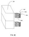
- FIG. 4Eis an isometric view of the buffering stations 1601 in accord with the present invention.
- FIG. 5Ais a side view that illustrates one embodiment of a coater chamber wherein the present invention may be used to advantage.
- FIG. 5Bis a side view that illustrates one embodiment of a developer chamber wherein the present invention may be used to advantage.
- FIG. 6is a plan view of a twin coater/developer chamber 350 according to the present invention.
- FIG. 7Ais a side view that illustrates one embodiment of a chill chamber wherein the present invention may be used to advantage.
- FIG. 7Bis a side view that illustrates one embodiment of a bake chamber wherein the present invention may be used to advantage.
- FIG. 7Cis a side view that illustrates one embodiment of a HMDS process chamber wherein the present invention may be used to advantage.
- FIG. 8Ais an isometric view illustrating one embodiment of a dual blade 6-axis articulated robot assembly according to the present invention.
- FIG. 8Bis an isometric view illustrating one embodiment of the dual blade assembly shown in FIG. 8A .
- FIG. 8Cis an isometric view illustrating one embodiment of the dual blade assembly shown in FIG. 8A .
- FIG. 8Dis an isometric view illustrating one embodiment of a single blade 6-axis articulated robot assembly wherein the present invention may be used to advantage.
- FIG. 8Eis an isometric view illustrating one embodiment of the single blade assembly shown in FIG. 8D .
- FIG. 8Fis an isometric view illustrating one embodiment of a dual blade 6-axis articulated robot assembly and slide assembly according to the present invention.
- FIG. 8Gillustrates a cross-sectional view of a dual blade assembly where the blades are positioned to transfer substrates from a pair of cassettes.
- FIG. 8Hillustrates a cross-sectional view of a dual blade assembly where the blades are positioned to transfer substrates from buffering stations.
- FIG. 8Iillustrates a cross-sectional view of a single blade assembly where the blade is positioned to transfer a substrate from a buffer station.
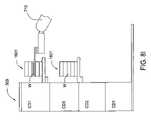
- FIG. 9Ais an isometric view of one embodiment of a bake chamber, a chill chamber and a robot adapted to transfer the substrate between the chambers.
- FIG. 9Bis an isometric view of one embodiment of a bake chamber, a chill chamber and a robot adapted to transfer the substrate between the chambers.
- FIG. 9Cis an isometric view showing the opposing side of the view shown in FIG. 9A which illustrates the robot adapted to transfer the substrate between the chambers.
- FIG. 10Ais an isometric view of one embodiment of a bake/chill chamber 800 .
- FIG. 10Bis an isometric view showing the opposing side of the view shown in FIG. 10A which illustrates the robot adapted to transfer the substrate between the chambers.
- FIG. 11is a plan view of a processing system illustrated in FIG. 2A that illustrates a transfer path of a substrate through the cluster tool following the process sequence illustrated in FIG. 3 .
- FIG. 12is a plan view of a processing system illustrated in FIG. 2A that illustrates a non-orthogonal robot trajectory.
- FIG. 13is an isometric view showing a processing chamber accessible to robots from non-orthogonal directions.
- FIG. 14is a plan view of a processing system illustrated in FIG. 2A that illustrates repositioning of robots.
- the present inventiongenerally provides an apparatus and method for processing substrates using a multi-chamber processing system (e.g., a cluster tool) that has an increased system throughput, increased system reliability, and a more repeatable wafer processing history (or wafer history) within the cluster tool.
- a multi-chamber processing systeme.g., a cluster tool
- the cluster toolis adapted to perform a track lithography process in which a substrate is coated with a photosensitive material, is then transferred to a stepper/scanner, which exposes the photosensitive material to some form of radiation to form a pattern in the photosensitive material, and then certain portions of the photosensitive material are removed in a developing process completed in the cluster tool.
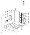
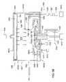
- FIGS. 1A and 1Bare isometric views of one embodiment of a cluster tool 10 that illustrates a number of the aspects of the present invention that may be used to advantage.
- One embodiment of the cluster tool 10as illustrated in FIGS. 1A and 1B , has a shape of a box which has four walls formed by a front end enclosure 104 , a front module 306 , a central module 310 , and a rear module 50 .
- the front end enclosure 104generally contains one or more pod assemblies 105 (e.g., items 105 A-D) configured to support one or more substrates.
- the front module 306generally contains a front end robot 108 , first and second processing racks 308 and 309 disposed on opposite sides of the front end robot 108 .
- the central module 310generally contain a first central processing rack 312 , a second central processing rack 314 , and a central robot 107 .
- a buffer rack 155is generally disposed between the front robot 108 and the central robot 107 adapted to be accessible by both robots 107 and 108 .
- the buffer rack 155may be positioned in suitable locations to avoid collisions between robots, improve throughput and/or serve as depair stations.
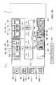
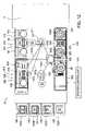
- FIG. 2Aillustrates a plan view of the cluster tool 10 illustrated in FIG. 1A .
- the front module 306may contain a first processing rack 308 and a second processing rack 309
- the central module 310may contain a first central processing rack 312 and a second central processing rack 314 .
- a plurality of buffering stations 1601is generally disposed near the border between the front module 306 and the central module 310 .
- the buffering stations 1601are configured to support one or more substrates and are accessible from more than one angle so that the robots 107 and 108 may access the buffering stations 1601 from two different directions, therefore, avoid collision and eliminate time used for collision avoidance.
- the rear module 50may contain a stepper/scanner 5 .
- the front end robot 108is adapted to transfer substrates between a cassette 106 mounted in a pod assembly 105 , the first processing rack 308 , the second processing rack 309 , the first central processing rack 312 , the second central processing rack 314 , the buffering stations 1601 , and/or the central robot 107 .
- the central robot 107is adapted to transfer substrates between the first processing rack 308 , the second processing rack 309 , the first central processing rack 312 , the second central processing rack 314 , the front end robot 108 , the buffering stations 1601 , and/or the stepper/scanner 5 .
- the front end robot 108 , and the central robot 107are articulated robots (described below).
- the front end robot 108is positioned in a central location between the first processing rack 308 and a second processing rack 309 of the front module 306 .
- the central robot 107is positioned in a central location between the first central processing rack 312 and a second central processing rack 314 of the central module 310 .
- a system controller 101is used to control all of the components and processes performed in the cluster tool 10 .
- the system controller 101is generally adapted to communicate with the stepper/scanner 5 , monitor and control aspects of the processes performed in the cluster tool 10 , and is adapted to control all aspects of the complete substrate processing sequence.
- FIG. 2Bis a plan view of another embodiment of the cluster tool 10 , which is similar to the embodiment shown in FIG. 2A , with the addition of a rear module 316 which may be attached to a stepper/scanner 5 .
- the front module 306may contain a first processing rack 308 and a second processing rack 309
- the central module 310may contain a first central processing rack 312 and a second central processing rack 314
- the rear module 316may contain a first rear processing rack 318 and a second rear processing rack 319 .
- a plurality of buffering stations 1601is generally disposed near the border between the front module 306 and the central module 310 .
- the front end robot 108is adapted to transfer substrates between a cassette 106 mounted in a pod assembly 105 , the first processing rack 308 , the second processing rack 309 , the first central processing rack 312 , the second central processing rack 314 , the buffering stations 1601 , and/or the central robot 107 .
- the central robot 107is adapted to transfer substrates between the first processing rack 308 , the second processing rack 309 , the first central processing rack 312 , the second central processing rack 314 , the first rear processing rack 318 , the second rear processing rack 319 , the front end robot 108 , the buffering stations 1601 , and/or the rear robot 109 .
- the rear robot 109is adapted to transfer substrates between the first central processing rack 312 , the second central processing rack 314 , the first rear processing rack 318 , the second rear processing rack 319 , the central robot 107 , and/or the stepper/scanner 5 .
- one or more of the front end robot 108 , the central robot 107 , and the rear robot 109are articulated robots (described below).
- the rear robot 109is positioned in a central location between the first rear processing rack 318 and a second rear processing rack 319 of the rear module 316 .
- FIGS. 2A and 2Bmay be advantageous since the gap formed between the processing racks forms a relatively open space that will allow maintenance personnel access to cluster tool components that have become inoperable. As shown in FIGS. 2A and 2B , in one aspect of the invention, the gap is as wide as the space between the processing racks and as high the height of the processing racks. Since system down-time and system availability are important components in determining the CoO for a given tool, the ability to easily access and maintain the cluster tool components have an advantage over other prior art configurations.
- FIG. 2Cis a plan view of yet another embodiment of the cluster tool 10 , which is similar to the embodiment shown in FIG. 2A , with the addition of a slide assembly 714 ( FIG. 8F ) which allows the base of the front end robot 108 and the central robot 107 to translate along the length (items A 1 and A 2 , respectively) of the cluster tool.
- This configurationextends the reach of each of the robots and improves the “robot overlap.”
- Robot overlapis the ability of a robot to access processing chambers in the processing rack of other modules. While FIG.
- FIG. 2Cillustrates the front end robot 108 and the central robot 107 on a single slide assembly 714
- other embodimentsmay include having each of the robots (Items 107 and 108 ) on their own slide assembly or only one of the robots mounted on a slide assembly and the other mounted to the floor or system frame, without varying from the scope of the invention.
- FIG. 2Dis a plan view of yet another embodiment of the cluster tool 10 , which is similar to the embodiment shown in FIG. 2B , with the addition of two slide assemblies 714 A-B (described in FIG. 8F ) which allows the base of the front end robot 108 and the base of the central robot 107 and rear robot 109 to translate along the length (items A 1 , A 2 and A 3 , respectively) of the cluster tool 10 . While FIG.
- 2Dillustrates the front end robot 108 on one slide assembly 714 A and the central robot 107 and the rear robot 109 on a single slide assembly 714 B
- other embodimentsmay include having one or more of the robots (Items 107 , 108 and 109 ) on their own slide assembly (not shown), on a shared slide assembly or all three on a single slide assembly (not shown), without varying from the scope of the invention.
- buffering stationssuch as the buffering stations 1601 in cluster tool 10 of FIGS. 2A-D , may be positioned in different locations in a cluster tool depending on the needs.
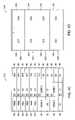
- FIG. 3illustrates one embodiment of a series of method steps 501 that may be used to deposit, expose and develop a photoresist material layer formed on a substrate surface.
- the lithographic processmay generally contain the following: a remove substrate from pod 508 A step, a BARC coat step 510 , a post BARC bake step 512 , a post BARC chill step 514 , a photoresist coat step 520 , a post photoresist coat bake step 522 , a post photoresist chill step 524 , an optical edge bead removal (OEBR) step 536 , an exposure step 538 , a post exposure bake (PEB) step 540 , a post PEB chill step 542 , a develop step 550 , and a place in pod step 508 B.
- the sequence of the method steps 501may be rearranged, altered, one or more steps may be removed, or two or more steps may be combined into a single step without varying from the basic scope of the invention.
- the remove substrate from pod 508 A stepis generally defined as the process of having the front end robot 108 remove a substrate from a cassette 106 resting in one of the pod assemblies 105 .
- a cassette 106containing one or more substrates “W”, is placed on the pod assembly 105 by the user or some external device (not shown) so that the substrates can be processed in the cluster tool 10 by a user-defined substrate processing sequence controlled by software retained in the system controller 101 .
- the BARC coat step 510or bottom anti-reflective coating process (hereafter BARC), is used to deposit an organic material over a surface of the substrate.
- the BARC layeris typically an organic coating that is applied onto the substrate prior to the photoresist layer to absorb light that otherwise would be reflected from the surface of the substrate back into the photoresist during the exposure step 538 performed in the stepper/scanner 5 . If these reflections are not prevented, optical standing waves will be established in the photoresist layer, which cause feature size(s) to vary from one location to another depending on the local thickness of the photoresist layer.
- the BARC layermay also be used to level (or planarize) the substrate surface topography, since surface topography variations are invariably present after completing multiple electronic device fabrication steps.
- the BARC materialfills around and over the features to create a flatter surface for photoresist application and reduces local variations in photoresist thickness.
- the BARC coat step 510is typically performed using a conventional spin-on photoresist dispense process in which an amount of the BARC material is deposited on the surface of the substrate while the substrate is being rotated, which causes a solvent in the BARC material to evaporate and thus causes the material properties of the deposited BARC material to change.
- the air flow and exhaust flow rate in the BARC processing chamberis often controlled to control the solvent vaporization process and the properties of the layer formed on the substrate surface.
- the post BARC bake step 512is used to assure that all of the solvent is removed from the deposited BARC layer in the BARC coat step 510 , and in some cases to promote adhesion of the BARC layer to the surface of the substrate.
- the temperature of the post BARC bake step 512is dependent on the type of BARC material deposited on the surface of the substrate, but will generally be less than about 250° C.
- the time required to complete the post BARC bake step 512will depend on the temperature of the substrate during the post BARC bake step, but will generally be less than about 60 seconds.
- the post BARC chill step 514is used to assure that the time the substrate is at a temperature above ambient temperature is controlled so that every substrate sees the same time-temperature profile; thus process variability is minimized. Variations in the BARC process time-temperature profile, which is a component of a substrate's wafer history, can have an effect on the properties of the deposited film layer and thus is often controlled to minimize process variability.
- the post BARC chill step 514is typically used to cool the substrate after the post BARC bake step 512 to a temperature at or near ambient temperature. The time required to complete the post BARC chill step 514 will depend on the temperature of the substrate exiting the post BARC bake step, but will generally be less than about 30 seconds.
- the photoresist coat step 520is used to deposit a photoresist layer over a surface of the substrate.
- the photoresist layer deposited during the photoresist coat step 520is typically a light sensitive organic coating that is applied onto the substrate and is later exposed in the stepper/scanner 5 to form the patterned features on the surface of the substrate.
- the photoresist coat step 520is a typically performed using conventional spin-on photoresist dispense process in which an amount of the photoresist material is deposited on the surface of the substrate while the substrate is being rotated, thus causing a solvent in the photoresist material to evaporate and the material properties of the deposited photoresist layer to change.
- the air flow and exhaust flow rate in the photoresist processing chamberis controlled to control the solvent vaporization process and the properties of the layer formed on the substrate surface. In some cases it may be necessary to control the partial pressure of the solvent over the substrate surface to control the vaporization of the solvent from the photoresist during the photoresist coat step by controlling the exhaust flow rate and/or by injecting a solvent near the substrate surface.
- the substrateis first positioned on a spin chuck 1033 in a coater chamber 60 A.
- a motorrotates the spin chuck 1033 and substrate while the photoresist is dispensed onto the center of the substrate. The rotation imparts an angular torque onto the photoresist, which forces the photoresist out in a radial direction, ultimately covering the substrate.
- the post photoresist coat bake step 522is used to assure that most, if not all, of the solvent is removed from the deposited photoresist layer in the photoresist coat step 520 , and in some cases to promote adhesion of the photoresist layer to the BARC layer.
- the temperature of the post photoresist coat bake step 522is dependent on the type of photoresist material deposited on the surface of the substrate, but will generally be less than about 250° C.
- the time required to complete the post photoresist coat bake step 522will depend on the temperature of the substrate during the post photoresist bake step, but will generally be less than about 60 seconds.
- the post photoresist chill step 524is used to control the time the substrate is at a temperature above ambient temperature so that every substrate sees the same time-temperature profile and thus process variability is minimized. Variations in the time-temperature profile can have an affect on properties of the deposited film layer and thus is often controlled to minimize process variability.
- the temperature of the post photoresist chill step 524is thus used to cool the substrate after the post photoresist coat bake step 522 to a temperature at or near ambient temperature.
- the time required to complete the post photoresist chill step 524will depend on the temperature of the substrate exiting the post photoresist bake step, but will generally be less than about 30 seconds.
- the optical edge bead removal (OEBR) step 536is a process used to expose the deposited light sensitive photoresist layer(s), such as the layers formed during the photoresist coat step 520 and the BARC layer formed during the BARC coat step 510 , to a radiation source (not shown) so that either or both layers can be removed from the edge of the substrate and the edge exclusion of the deposited layers can be more uniformly controlled.
- the wavelength and intensity of the radiation used to expose the surface of the substratewill depend on the type of BARC and photoresist layers deposited on the surface of the substrate.
- An OEBR toolcan be purchased, for example, from USHIO America, Inc. Cypress, Calif.
- the exposure step 538is a lithographic projection step applied by a lithographic projection apparatus (e.g., stepper scanner 5 ) to form a pattern which is used to manufacture integrated circuits (ICs).
- the exposure step 538forms a circuit pattern corresponding to an individual layer of the integrated circuit (IC) device on the substrate surface, by exposing the photosensitive materials, such as, the photoresist layer formed during the photoresist coat step 520 and the BARC layer formed during the BARC coat step 510 (photoresist) of some form of electromagnetic radiation.
- the stepper/scanner 5which may be purchased from Cannon, Nikon, or ASML.
- the post exposure bake (PEB) step 540is used to heat a substrate immediately after the exposure step 538 in order to stimulate diffusion of the photoactive compound(s) and reduce the effects of standing waves in the photoresist layer.
- the PEB stepalso causes a catalyzed chemical reaction that changes the solubility of the photoresist.
- the control of the temperature during the PEBis critical to critical dimension (CD) control.
- the temperature of the PEB step 540is dependent on the type of photoresist material deposited on the surface of the substrate, but will generally be less than about 250° C.
- the time required to complete the PEB step 540will depend on the temperature of the substrate during the PEB step, but will generally be less than about 60 seconds.
- the post exposure bake (PEB) chill step 542is used to assure that the time the substrate is at a temperature above ambient temperature is controlled, so that every substrate sees the same time-temperature profile and thus process variability is minimized. Variation in the PEB process time-temperature profile can have an effect on properties of the deposited film layer and thus is often controlled to minimize process variability.
- the temperature of the post PEB chill step 542is thus used to cool the substrate after the PEB step 540 to a temperature at or near ambient temperature.
- the time required to complete the post PEB chill step 542will depend on the temperature of the substrate exiting the PEB step, but will generally be less than about 30 seconds.
- the develop step 550is a process in which a solvent is used to cause a chemical or physical change to the exposed or unexposed photoresist and BARC layers to expose the pattern formed during the exposure step 538 .
- the develop processmay be a spray or immersion or puddle type process that is used to dispense the developer solvent.
- a rinse stepmay be performed to rinse the solvent material from the surface of the substrate.
- the rinse solution dispensed on the surface of the substratemay contain deionized water and/or a surfactant.
- the insert the substrate in pod step 508 Bis generally defined as the process of having the front end robot 108 return the substrate to a cassette 106 resting in one of the pod assemblies 105 .
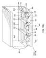
- FIG. 4A-Dillustrate side views of one embodiment of a first processing rack 308 , a second processing rack 309 , a first central processing rack 312 , a second central processing rack 314 , a first rear processing rack 318 and a second rear processing rack 319 , that contain multiple substrate processing chambers to perform various aspects of the substrate processing sequence.
- 4A-Dmay contain one or more process chambers, such as, one or more coater chambers 60 A, one or more developer chambers 60 B, one or more chill chambers 80 , one or more bake chambers 90 , one or more PEB chambers 130 , one or more support chambers 65 , one or more OEBR chambers 62 , one or more twin coater/developer chambers 350 , one or more bake/chill chambers 800 , and/or one or more HMDS chambers 70 , which are further described below.
- the orientation, type, positioning and number of process chambers shown in the FIGS. 4A-Dare not intended to be limiting as to the scope of the invention, but are intended to illustrate the various embodiments of the invention. In one embodiment, as shown in FIGS.
- the process chambersare stacked vertically, or one chamber is positioned substantially above another chamber, to reduce the footprint of the cluster tool 10 .
- Minimizing the cluster tool footprintis often an important factor in developing a cluster tool, since the clean room space, where the cluster tool may be installed, is often limited and very expensive to build and maintain.
- FIG. 4Aillustrates a side view of the first processing rack 308 as viewed from outside the cluster tool 10 while facing the front end robot 108 and thus will coincide with the views shown in FIGS. 2A-D .
- the first processing rack 308contains twelve bake/chill chambers 800 (labeled BC 1 - 12 ). A detailed description of a bake/chill chamber may be found in FIG. 18 of co-pending U.S. patent application Ser. No. 11/112,281, filed Apr. 22, 2005, which is herein incorporated as reference.
- FIG. 4Billustrates a side view of the second processing rack 309 as viewed from outside the cluster tool 10 while facing the front end robot 108 and thus will coincide with the view shown in FIGS. 2A-D .
- the second processing rack 309contains four coater/developer chambers 60 (labeled CD 1 - 4 ) and four support chambers 65 (labeled S 1 - 4 ).
- the four support chambers 65are replaced with four coater/developer chambers 60 .
- FIG. 4Cillustrates a side view of the first central processing rack 312 , or the first rear processing rack 318 , as viewed from outside the cluster tool 10 while facing the central robot 107 , or rear robot 109 , and thus will coincide with the views shown in FIGS. 2A-D .
- FIG. 4Cillustrates a side view of the first central processing rack 312 , or the first rear processing rack 318 , as viewed from outside the cluster tool 10 while facing the central robot 107 , or rear robot 109 , and thus will coincide with the views shown in FIGS. 2A-D .
- FIG. 4Cillustrates a side view of the first central processing rack 312 , or the first rear processing rack 318 , as viewed from outside the cluster tool 10 while facing the central robot 107 , or rear robot 109 , and thus will coincide with the views shown in FIGS. 2A-D .
- FIG. 4Cillustrates a side view of the first central processing rack 312 , or the first rear processing rack 318
- the first central processing rack 312or the first rear processing rack 318 , contains eight chill chambers 80 (labeled C 1 - 8 ), fourteen bake chambers 90 (labeled B 1 , B 2 , B 3 , B 5 , B 6 , B 7 , etc.), four OEBR chambers 62 (labeled OEBR 1 - 4 ), and six PEB chambers 130 (labeled PEB 1 - 6 ).
- the first central processing rack 312 , or the first rear processing rack 318may be arranged like the configuration illustrated in FIG. 4A , which contains twelve chill chambers 80 and twenty four bake chambers 90 .
- FIG. 4Dillustrates a side view of the second central processing rack 314 , or the second rear processing rack 319 , as viewed from outside the cluster tool 10 while facing the central robot 107 (or rear robot 109 ) and thus will coincide with the views shown in FIGS. 2A-D .
- the second central processing rack 314 , or the second rear processing rack 319contains four twin coater/developer chambers 350 , which contain four pairs of process chambers 370 that may be configured as coater chambers 60 A, as developer chambers 60 B or combinations thereof.
- FIG. 4Eillustrates an isometric view of the buffering stations 1601 in accordance with the present invention.
- the buffering stations 1601are attached to a processing rack, for example, the second processing rack 309 of the front module 306 .
- Each of the buffering station 1601may comprise a plurality of substrate support 1602 vertically stacked together.
- Each substrate support 1602may be accessible from a first direction 1603 and a second direction 1604 so that two robots may approach the buffering stations 1601 at the same time without collision, hence, eliminating the time consumed for collision avoidance and improving system throughput and reliability.
- two buffering stations 1601may be disposed vertically with a vertical distance matching the distance between the duel blades of a dual blade assembly so that two substrates may be transferred to and from the buffering stations 1601 simultaneously (as described in FIG. 8H ).
- the coater/developer chamber 60is a processing chamber that may be adapted to perform, for example, the BARC coat step 510 , the photoresist coat step 520 , and the develop step 550 , which are shown in FIG. 3 .
- the coater/developer chamber 60may generally be configured into two major types of chambers, a coater chamber 60 A, shown in FIG. 5A , and a developer chamber 60 B, shown in FIG. 5B (discussed below).
- FIG. 5Ais a vertical sectional view of one embodiment of the coater chamber 60 A, that may be adapted to perform the BARC coat step 510 , the photoresist coat step and the anti-reflective top coat step 530 .
- the coater chamber 60 Amay contain an enclosure 1001 , a gas flow distribution system 1040 , a coater cup assembly 1003 , and a fluid dispense system 1025 .
- the enclosure 1001generally contains side walls 1001 A, a base wall 1001 B, and a top wall 1001 C.
- the coater cup assembly 1003which contains the processing region 1004 in which the substrate “W” is processed, also contains a cup 1005 , a rotatable spin chuck 1034 and a lift assembly 1030 .
- the gas flow distribution system 1040is generally adapted to deliver a uniform flow of a gas through the enclosure 1001 and coater cup assembly 1003 to the exhaust system 1012 .
- the rotatable spin chuck 1034generally contains a spin chuck 1033 , a shaft 1032 and a rotation motor 1031 , and a vacuum source 1015 .
- the spin chuck 1033which is attached to the rotation motor 1031 through the shaft 1032 , contains a sealing surface 1033 A that is adapted to hold the substrate while the substrate is being rotated. The substrate may be held to the sealing surface 1033 A by use of a vacuum generated by the vacuum source 1015 .
- the cup 1005manufactured from a material, such as, a plastic material, or other materials that is compatible with the processing fluids delivered from the fluid dispense system 1025 .
- the fluid dispense system 1025generally contains one or more fluid source assemblies 1023 which deliver one or more solution to the surface of a substrate mounted on the spin chuck 1033 .
- the rotation motor 1031is adapted to rotate a 300 mm semiconductor substrate between about 1 revolution per minute (RPM) and about 4000 RPM.
- RPMrevolution per minute
- An example of an exemplary coater processing chamberis further described in the copending U.S. patent application Ser. No. 11/112,281, filed Apr. 22, 2005, which is herein incorporated by reference.
- the developer chamber 60 Bgenerally contains all of the components contained in the coater chamber 60 A and thus some components of the developer chamber 60 B that are the same or similar to those described with reference to the developer chamber 60 B, have the same numbers. Accordingly, like numbers have been used where appropriate.
- the developer chamber 60 Bcontains a fluid distribution device 1070 , described above, is adapted to deliver a uniform flow of a developer processing fluid to the surface of the substrate during the developing process.
- An example of an exemplary developer chamberis further described in the co-pending U.S. patent application Ser. No. 11/112,281, filed Apr. 22, 2005, which is herein incorporated by reference.
- FIG. 6is a plan view of one embodiment of a twin coater/developer chamber 350 that contains two separate process chambers 370 and a central region 395 .
- This configurationis advantageous since it allows some common components in the two chambers to be shared, thus increasing system reliability and reducing the system cost, complexity and footprint of the cluster tool.
- the process chamber 370generally contains all of the processing components described above in conjunction with the coater chamber 60 A or developer chamber 60 B, except the two chambers are adapted to share a fluid dispense system 1025 .
- the central region 395contains a shutter 380 and a plurality of nozzles 391 that are contained in a nozzle holder assembly 390 .
- the fluid dispense system 1025 used in the coater or developer chambersmay contain one or more fluid source assemblies 1023 which deliver one or more processing fluid to the surface of a substrate mounted on the spin chuck 1033 .
- Each nozzle 391contained in the fluid source assemblies 1023 , is typically connected to a supply tube 1026 , a pump 1022 , a filter 1021 , a suck back valve 1020 and a fluid source 1019 , and is adapted to dispense a single type of processing fluid. Therefore, each fluid source assembly 1023 can be used in either the left or right process chambers 370 , thus reducing the redundancy required to in each processing chamber.
- the nozzle arm assembly 360is positioned over the right process chamber 370 to dispense a processing fluid on a substrate “W” retained on the spin chuck 1033 .
- the nozzle arm assembly 360may contain an arm 362 and nozzle holding mechanism 364 .
- the nozzle arm assembly 360is attached to an actuator 363 that is adapted to transfer and position the nozzle arm assembly 360 in any position along the guide mechanism 361 .
- the actuatoris adapted to move the nozzle arm assembly 360 vertically to correctly position the nozzle 391 over the substrate during processing and also enable the nozzle holding mechanism 364 to pick-up and drop-off the nozzles 391 from the nozzle holder assembly 390 .
- the system controller 101is adapted to control the position of the nozzle arm assembly 360 so that the nozzle holding mechanism 364 can pick-up and drop-off nozzles 391 from the nozzle holder assembly 390 .
- a shutter 380is adapted to move vertically to close and isolate one process chamber 370 from the central region 395 and thus the other process chamber 370 during processing to prevent cross contamination of the substrates during processing.
- the shutter 380is adapted to sealably isolate one process chamber 370 from the central region 395 and thus the other process chamber 370 during processing.
- Conventional o-ring and/or other lip sealsmay be used to allow the shutter to sealably isolate the two processing chambers.
- An example of an exemplary twin coater/developer chamberis further described in the co-pending U.S. patent application Ser. No. 11/112,281, filed Apr. 22, 2005, which is herein incorporated by reference.
- FIG. 7Ais a vertical sectional view that illustrates one embodiment of a chill chamber 80 that may be adapted to perform the post BARC chill step 514 , the post photoresist chill step 524 , the post top coat chill step 534 , the post PEB chill step 542 and/or the post develop chill step 554 .
- the chill chamber 80generally contains an enclosure 86 , chill plate assembly 83 , a support plate 84 , and a lift assembly 87 .
- the enclosure 86is formed by a plurality of walls (items 86 B-D and item 85 ) which isolate the processes performed in the chill chamber 80 from the surrounding environment to form a processing region 86 A.
- the enclosureis adapted to thermally isolate and minimize the possibility of atmospheric contamination in the chill chamber 80 .
- An example of an exemplary chill chamberis further described in the co-pending U.S. patent application Ser. No. 11/112,281, filed Apr. 22, 2005, which is herein incorporated by reference.
- FIG. 7Bis a side view that illustrates one embodiment of a bake chamber 90 that may be adapted to perform the post BARC bake step 512 , the post photoresist coat bake step 522 , the post top coat bake step 532 and/or the post develop bake step 552 .
- the bake chamber 90generally contains an enclosure 96 , bake plate assembly 93 , a support plate 94 , and a lift assembly 97 .
- the enclosure 96generally contains a plurality of walls (items 96 B-D and element 95 ) which tend to isolate the processes performed in the bake chamber 90 from the surrounding environment to form a processing region 96 A.
- the enclosureis adapted to thermally isolate and minimize contamination of the bake chamber 90 from the surrounding environment.
- An example of an exemplary bake chamberis further described in the co-pending U.S. patent application Ser. No. 11/112,281, filed Apr. 22, 2005, which is herein incorporated by reference.
- FIG. 7Cis a side view that illustrates one embodiment of a HMDS process chamber 70 that may be adapted to perform the HMDS processing step 511 .
- the HMDS process chamber 70contains some of the components contained in the bake chamber 90 shown in FIG. 7B and thus some components of the HMDS process chamber 70 are the same or similar to those described with reference to the bake chamber 90 , described above.
- An example of an exemplary HMDS chamberis further described in the co-pending U.S. patent application Ser. No. 11/112,281, filed Apr. 22, 2005, which is herein incorporated by reference.
- an insoluble photoresist materialis transformed into a soluble material.
- components in the photoresist that contain photoacid generators (or PAGS)generate an organic acid that can attack the unexposed areas of the photoresist and affect the sharpness of the pattern formed in the photoresist layer during the exposure process.
- the attack of the unexposed photoresistis thus affected by the migration of the generated photoacid, which is a diffusion dominated process. Since the photoacid attack of the formed pattern is a diffusion dominated process, the rate of attack is dependent on two related variables, time and temperature. The control of these variables are thus important in assuring that the critical dimension (CD) uniformity is acceptable and consistent from substrate to substrate.
- CDcritical dimension
- the PEB step 540is performed in a bake chamber 90 as shown in FIG. 7B .
- the PEB step 540is performed in a HMDS process chamber 70 where a temperature controlled gas is delivered from the purge gas source 71 C to the processing region 76 , to heat or cool the substrate retained on the HMDS bake plate assembly 73 .
- a temperature controlled gasis delivered from the purge gas source 71 C to the processing region 76 , to heat or cool the substrate retained on the HMDS bake plate assembly 73 .
- FIG. 8Ais an isometric view of one embodiment of the central robot 107 containing an articulated robot assembly 702 (hereafter AR assembly 702 ).
- the AR assembly 702is adapted to transfer substrates to and from the various process chambers contained in the front end processing rack 52 , the first central processing rack 152 , the second central processing rack 154 and/or the rear processing rack 202 .
- the second central processing rack 154has been removed from FIG. 8A to highlight and clarify the components contained in this embodiment.
- the AR assembly 702generally contains articulated robot 710 and a dual blade assembly 705 .
- the articulated robot 710is generally a 6-axis articulated robot which can be purchased from Mitsubishi Electric Corporation, of Tokyo, Japan, Kawasaki Robotics (USA), Inc.
- the 6-axis articulated robotis a model number TX90 purchased from Staubli Corp. of Duncan, S.C.
- the articulated robot 710has a robot base 713 A and a mechanical interface 713 B, which connect the robot to the cluster tool and the end-effector assembly (e.g., dual blade assembly 705 , blade assembly 706 , etc.) to the robot, respectively.
- the 6-axis articulated robotis advantageous since the reach of the articulated robot is far superior from conventional robots due to its multiple axis and multiple linkage design, the reach of multiple articulated robots can more easily “overlap” since the motion of the end-effector, which retains and transfers the substrate(s), is not linked to motion of the robot base 713 A which allows the robots to more effectively avoid each other while transferring substrates, and/or the reliability of the articulated robots exceeds most conventional robots.
- the dual blade assembly 705generally contains a support 720 , and two or more blade assemblies 715 (e.g., first blade assembly 715 A, a second blade assembly 715 B, etc.).
- the support 720attaches to and is guided by the articulated robot 710 so that a blade in a first blade assembly 715 A and a blade in a second blade assembly 715 B can each pick-up and/or place a substrate in a two different processing chambers retained in a processing rack.
- the pitch(see item “A”), or the distance, between the robot blades is fixed by the distance between the first supporting surface 720 A and second supporting surface 720 B, and is designed to coincide with the pitch between two of the processing chambers retained in the processing racks.
- the distance between the transfer position of the bake chambers labeled B 1 and B 4would coincide with the pitch between the coater/developer chambers labeled CD 1 and CD 2 in the front end processing rack 52 , so that after completing the BARC coat step 510 the substrates could then be transferred to bake chambers labeled B 1 and B 4 to complete the post BARC bake step 512 .
- the pitch “A”is generally defined as the distance, or spacing, between the blades 711 A-B in a normal direction to the substrate receiving surfaces 712 A-B.
- the pitch(see item “A”), is a distance between about 100 mm and about 1200 mm, and preferably between about 300 mm and about 700 mm. While the dual blade assembly 705 is illustrated in conjunction with the articulated robot assembly 702 , other configurations may utilize the dual blade assembly 705 on other types of robots without varying from the basic scope of the invention.
- the substrate receiving surfaces 712 A-Bare adapted to retain a substrate positioned on the blade (not shown) by use of an edge gripping mechanism that holds the substrate in position on the robot blade.
- the edge gripping mechanismcan be adapted to grab the edge of the substrate at multiple points (e.g., 3 points) to hold and retain the substrate.
- each blade assembly 715(e.g., first blade assembly 715 A or second blade assembly 715 B), generally contains one or more robot blade actuators 721 (see items 721 A- 721 B) and one or more robot blades 711 (see items 711 A- 711 B).
- the robot blade actuators 721may be a direct drive linear brushless servomotor or other equivalent device that is able to control the motion and position of the robot blade 711 .
- the pitch between the robot bladeswill not affected by the actuation, or translation, of one robot blade relative to another robot blade, since it is preferred that the actuated blade translate in a plane that is parallel to the other robot blade.
- FIG. 8Cillustrates one embodiment of the dual blade assembly 705 which contains one pair of blade assemblies 715 A and 715 C mounted on the first supporting surface 720 A and a second pair of blade assemblies 715 B and 715 D mounted on the second supporting surface 720 B.
- FIG. 8Cfurther illustrates a configuration where robot blade 711 B is shown in an actuated position while the other blades (e.g., 715 A and 715 C-D) are shown in their retracted position.
- each robot blade 711(e.g., 711 A-D), contained in its respective blade assembly 715 (e.g., 715 A-D), may be independently actuated by use of the system controller (not shown) and its robot blade actuator 721 (e.g., 721 A-D).
- each robot blade 711 in each of the pairsmay be physically positioned in an orientation that is substantially horizontally aligned over each other and vertically spaced apart (often termed “over/under” configuration), so that a substrate can be retained on each blade at the same time.
- the over/under blade configurationmay be advantageous, for example, where the robot has to remove a substrate from a processing chamber prior to placing the next substrate to be processed in the same processing chamber, without having to leave its basic position to move the “removed” substrate to another chamber.
- this configurationmay allow the robot to fill up all of the blades and then transfer the substrates in groups to a desired location in the tool. For example, in FIG. 8C four substrates could be transferred on the four blades.
- This configurationalso has a further advantage that allows substrates transferred in groups to be ungrouped by dropping-off or picking-up the substrates one at a time from each of the blades 711 A-D.
- three or more stacked blades mounted on each of the supporting surfacesmay be used in place of the “pairs” of robot blades to further facilitate the transfer of multiple substrates in groups.
- the robotis adapted to “re-position,” e.g., flip, rotate, and/or detach, at least one of the robot blades so that the “re-positioned” blade(s) will not interfere with the process of transferring a substrate on another robot blade.
- a special position or chambere.g., support chambers
- the ability to re-position one or more of the robot bladesmay be especially useful when one or more processing chambers in a grouped transferring sequence is not operational, and thus will not allow a blade to enter the processing chamber, since it will allow other adjacent processing chamber positions to be utilized.
- FIGS. 8D and 8Eare isometric views of one embodiment of the front end robot 108 or the rear robot 109 containing a single blade type articulated robot assembly 703 .
- the single articulated robot assembly 703(hereafter SA robot assembly 703 ) is adapted to transfer substrates to and from the various process chambers contained in the front end processing rack 52 and the pod assembly 105 , or the rear processing rack 202 and stepper/scanner 5 , depending on whether the robot is a front end robot 108 or the rear robot 109 .
- the SA robot assembly 703generally contains a articulated robot 710 and a blade assembly 706 .
- the articulated robot 710is generally a 6-axis articulated robot which can be purchased from Mitsubishi Electric Corporation, of Tokyo, Japan, Kawasaki Robotics (USA), Inc., of Wixom, Mich., and Staubli Corp. of Duncan, S.C.
- the blade assembly 706generally contains a support 718 and a blade assembly 715 (e.g., first blade assembly 715 A), described above.
- the support 718attaches to and is guided by the articulated robot 710 so that robot blade 711 in a blade assembly 715 can pick-up and/or place a substrate in a processing chamber retained in a processing rack.
- the single blade articulated robot assembly 703may contain a pair of blade assemblies 715 (e.g., items 715 A and 715 C) such as one of the pairs illustrated and described in conjunction with FIG. 8C .
- the front end robot 108 or the rear robot 109are a dual blade assembly 705 as illustrated and described above in conjunction with FIGS. 8A-D and 14 A-B. This configuration will allow grouped transfer of the substrates throughout the system and thus increase throughput, CoO and system reliability.
- FIG. 8Fis an isometric view of one embodiment of a moveable articulated robot (e.g., AR assembly 702 is shown) that is adapted to allow the articulated robot base 713 to be translated and positioned along the length of a cluster tool by use of a slide assembly 714 .
- the articulated robot base 713is connected to an actuator assembly 717 of the slide assembly 714 , which is adapted to move the AR assembly 702 to a desired position in the cluster tool by use of commands from the system controller 101 .
- the slide assembly 714generally contains an actuator assembly 717 , a cover (not shown), and a base 716 .
- the base 716supports and mounts the AR assembly 702 and slide assembly components to the cluster tool.
- the coveris used to enclose the actuator assembly 717 and other slide assembly features to prevent generated particles from making their way to the processing chambers and prevent damage to these features during maintenance of the cluster tool.
- the actuator assembly 717may generally contain an actuator 719 and a guiding mechanism 723 .
- the actuator 719is a direct drive linear brushless servomotor, which through communication with the base component 719 A (e.g., secondary coil or “rotor” section) mounted on the base 716 and a slider 719 B (e.g., stator), is adapted to move the AR assembly 702 along the length of the slide assembly 714 .
- the base component 719 Ae.g., secondary coil or “rotor” section
- a slider 719 Be.g., stator
- a direct drive linear brushless servomotorthat may be purchased from Danaher Motion of Wood Dale, Ill. or Aerotech, Inc. of Pittsburgh, Pa.
- the actuator 719may be stepper motor or other type of actuator that can be used to position the robot.
- the guiding mechanism 723is mounted to the base 716 and is used to support and guide the robot as it is moved along the length of the slide assembly 714 .
- the guiding mechanism 723may be a linear ball bearing slides or a conventional linear guide, which are well known in the art.
- FIG. 8Fillustrates a single robot mounted to the slide assembly 714
- two or more robotsmay be affixed to the same slide assembly. This configuration can reduce cost by reducing the number of redundant parts and improve the precise motion of each of the robots relative each other.
- FIG. 8Fillustrates a dual blade articulated robot mounted to the slide assembly 714
- the type of robot or number of bladesis not intended to be limiting of the scope of the invention.
- FIG. 8Gillustrates a cross-sectional view of one embodiment of a robot having two fixed blades that are positioned to pick-up two substrates positioned in the two separate vertically stacked pod assemblies 105 .
- the multiple bladed robotis adapted to pick-up and/or drop-off substrates positioned in the two cassettes (item #s 106 A-B) to allow grouped substrate transferring process to be performed at the start and/or the end of the substrate transferring sequence.
- the cassettes and the pod assembliesare spaced a distance “A” apart so that a robot can access the substrates in similar positions in each cassette. In one aspect, the distance of “A” is about 600 mm.
- a region 731 Bmay be formed to allow the first blade 711 A to access a position in the lower cassette 106 B while allowing the lower robot blade 711 B to enter the region 731 B without colliding with the wall 731 C. While FIG.
- FIG. 8Gillustrates a configuration where the robot blades 711 A-B are fixed to the support surfaces 720 A-B of the support 720 , and thus do not utilize a robot blade actuator 721 , other embodiments having robot blade actuators can be used without varying from the basic scope of the invention.
- FIG. 8Hillustrates a cross-sectional view of one embodiment of a robot having two fixed blades that are positioned to pick-up two substrates positioned in the two separate vertically stacked buffering stations 1601 .
- the multiple bladed robotis adapted to pick-up and/or drop-off substrates positioned in the two buffering stations 1601 to allow grouped substrate transferring process to be performed in a substrate transferring sequence.
- the cassettes and the pod assembliesare spaced a distance “A” apart so that a robot can access the substrates in similar positions in each cassette.
- FIG. 8Iillustrates a cross-sectional view of one embodiment of a robot having a single blade that is positioned to pick-up a substrates positioned a buffering station 1601 . Allowing single substrate transferring provides flexibility to the processing sequence and balancing loads between the robots.
- FIGS. 9A-Cillustrate various embodiments of a shuttle robot 110 that can be adapted to transfer substrates between adjacent chambers in the various processing racks.
- the design heremay be advantageous for use when transferring substrates between a bake process chamber (e.g., bake chamber 90 , HMDS process chamber 70 , PEB chamber 130 , etc.) and a chill chamber 80 which are used in subsequent processing steps, for example, between the post BARC bake step 512 and the post BARC chill step 514 and the post photoresist coat bake step 522 and the post photoresist chill step 524 .
- a bake process chambere.g., bake chamber 90 , HMDS process chamber 70 , PEB chamber 130 , etc.
- a chill chamber 80which are used in subsequent processing steps, for example, between the post BARC bake step 512 and the post BARC chill step 514 and the post photoresist coat bake step 522 and the post photoresist chill step 524 .
- the shuttle robot 110is thus used to reduce the work load on the various system robots, such as, the front end robot 108 , the central robot 107 , and the rear robot 109 , thus allowing the system robots to do other tasks while the other processing steps are completed on the substrates.
- FIG. 9Ais an isometric view of one configuration in which the shuttle robot 110 is used to transfer substrates between three adjacent processing chambers, such as between two bake chambers 90 and a chill chamber 80 .
- This configurationmay thus be used between, for example, a bake chamber B 1 , chill chamber C 1 and bake chamber B 2 in the first central processing rack 152 shown in FIG. 4B .
- FIG. 9Bis an isometric view of one configuration in which the shuttle robot 110 is used to transfer substrates between two adjacent processing chambers, such as between a bake chamber 90 and a chill chamber 80 .
- This configurationmay thus be used between, for example, a bake chamber B 1 and chill chamber C 7 contained in the front end processing rack 52 shown in FIG. 4A , a PEB bake chamber PEB 1 and chill chamber C 3 contained in the rear processing rack 202 shown in FIG. 4D , or a HMDS process chamber P 1 and chill chamber C 1 contained in the front end processing rack 52 shown in FIG. 4A .
- FIG. 9Cis an isometric view of the backside of the adjacent processing chambers shown in FIG. 9A or 9 B which is intended to show an embodiment of the shuttle robot 110 .
- the shuttle robot 110generally contains a robot blade 111 and a shuttle robot actuator assembly 120 .
- a shuttle robot actuator assembly 120generally contains a robot blade actuator 112 , a slide assembly 113 and a robot drive assembly 119 .
- the robot blade 111generally contains a substrate retaining area 111 A and a mounting region 111 B.
- the mounting region 111 Bis an area of the robot blade 111 that is used to attach the robot blade 111 to the robot blade actuator 112 (see mount 112 A).
- the substrate retaining area 111 Amay be adapted to act as a conventional vacuum chuck, which is attached to a vacuum generating source (not shown), to hold a substrate during the substrate transferring process.
- the robot blade actuator 112is a device that is used to raise and lower the robot blade 111 so that the substrate can be transferred from one processing chamber to another.
- the robot blade actuator 112is an air cylinder.
- a linear actuatore.g., linear brushless servo motor (not shown) is mounted between the robot blade actuator 112 and the robot blade 111 , so that the robot blade 111 can be extended and/or retracted (e.g., into or out of the chamber) to complete the substrate transfer process with the lift pins or other substrate retaining features in the processing chamber.
- the slide assembly 113is a linear ball bearing slide that guides the shuttle robot 110 as it transfers the substrates between the various processing chambers.
- the slide assembly 113generally contains a shuttle 113 A on which the robot blade actuator 112 is attached.
- the clamp 118is used to attach the shuttle 113 A to the belt 117 of the robot drive assembly 119 to allow the robot drive assembly 119 to move the robot blade 111 between the various processing chambers.
- the robot drive assembly 119is a belt and pulley type system which is used move the robot along the length of the slide assembly 113 .
- the robot drive assembly 119will generally contain two or more idler pulleys 116 A-B, a belt 117 and a motor 115 that is adapted to drive and control the position of the robot.
- the motor 115is a DC servomotor with an integrated encoder so that the system controller 101 can keep track of and control the position of the shuttle robot 110 .
- the belt and pulley type systemis replaced with a direct drive linear brushless servomotor that may be purchased from Danaher Motion of Wood Dale, Ill.
- FIG. 10Aillustrates one embodiment of an integrated bake/chill chamber 800 that may be used in conjunction with the various embodiments of the cluster tool.
- the integrated bake/chill chamber 800has three major processing regions: an input region 830 , a chill region 810 and a bake region 820 , which are adapted to perform a process sequence where various bake method steps (e.g., post BARC bake step 512 , PEB step 540 , etc.) and/or chilled method steps (e.g., post BARC chill step 514 , post PEB chill step 544 , etc.) are performed.
- the integrated bake/chill chamber 800may contain two or more access ports 802 (two shown in FIG.
- the enclosure 804generally contains an input station enclosure 804 A, a chill chamber enclosure 804 B and a bake chamber enclosure 804 C, that are adapted to isolate the various regions of the integrated bake/chill chamber 800 .
- the input region 830is used to receive a substrate from an external robot.
- the input region 830is generally an enclosed region that contains a substrate exchanging device, such as lift pins 836 or some other similar device, that is adapted to allow an external robot to pick up or drop-off a substrate in the integrated bake/chill chamber 800 .
- the input region 830is also configured to allow a chilled transfer arm assembly 832 to pick-up and drop off substrates from the lift pins 836 .
- the chilled transfer arm assembly 832generally contains a chilled blade 833 that has a blade receiving surface 834 and a plurality of cut-outs 835 that are adapted to allow the chilled blade 833 to pick-up, retain and drop-off substrates from the various substrate exchanging devices in the various processing regions of the integrated bake/chill chamber 800 .
- the chilled blade 833 of the chilled transfer arm assembly 832contains a heat exchanging device 837 ( FIG. 10B ) that is in thermal communication with the blade receiving surface 834 so that the temperature of a substrate positioned on the blade receiving surface 834 can be temperature controlled.
- the temperature of the heat exchanging device 837is monitored and controlled by use of a temperature controlling device 838 ( FIG.
- the heat exchanging device 837may be a thermal electric device and/or embedded heating elements so that the temperature of the substrate can be controlled.
- the heat exchanging device 837may contain a plurality of fluid channels (not shown) that are embedded in the chilled blade 833 , that are configured to allow a temperature controlled heat exchanging fluid to flow therethrough.
- the blade receiving surface 834may contain mechanical features (not shown) to retain a substrate on the receiving surface.
- the blade receiving surface 834may contain a plurality of vacuum ports (not shown) that are connected to a vacuum source (not shown) to retain the substrate and assure intimate contact between the substrate and the blade receiving surface 834 .
- FIG. 10Billustrates one embodiment of the chilled transfer arm assembly 832 that utilizes a chilled blade actuator assembly 839 , similar to the shuttle robot actuator assembly 120 described above in conjunction with FIG. 9C , which is used to control the position of the chilled blade assembly 832 in any of the various processing regions of the integrated bake/chill chamber 800 .
- the system controller 101is utilized to position, both vertically and horizontally, the chilled blade assembly 832 in any of the various processing regions of the integrated bake/chill chamber 800 .
- the chilled blade 833is positioned by use of a chilled blade actuator assembly 839 , on which is mounted one or more surfaces of the integrated bake/chill chamber 800 .
- the enclosure 804contains a plurality of enclosure cut-outs 806 , which allow the chilled blade 833 to transfer a substrate between the various processing regions of the integrated bake/chill chamber 800 .
- the chill region 810contains the chill chamber 80 components illustrated and described in reference to FIG. 7A .
- the enclosure 804 Bcontains one or more enclosure cut-outs 806 to allow the chilled transfer arm assembly 832 to facilitate the transfer of a substrate between the various processing regions of the integrated bake/chill chamber 800 .
- the bake region 820may contain all of the components of a bake chamber 90 , HMDS process chamber 70 , or a PEB chamber 130 as illustrated and described in reference to FIGS. 7B-D .
- the enclosure 804 Ccontains one or more enclosure cut-outs 806 to allow the chilled transfer arm assembly 832 to transfer a substrate between the various processing regions of the integrated bake/chill chamber 800 .
- an external robotdelivers the substrate to the lift pins 836 of the input region 830 through an access port 802 .
- the chilled blade 833which is positioned below the lift pins 836 , then moves vertically to remove the substrate from the lift pins 836 and positions the substrate on the blade receiving surface 834 .
- the chilled blade 833is then moved to the bake region 820 where the chilled blade 833 deposits the substrate and then exits the bake region 820 so that a bake process can be performed on the substrate.
- the chilled blade 834picks up the substrate from the bake region 820 , transfers the substrate to a substrate exchanging device in the chill region 810 , and then exits the chill region 810 .
- the substrateis removed from the chill region 810 through the access port 802 by use of the external robot.
- the chilled blade 833removes the substrate from the chill region 810 and deposits the substrate on the lift pins 836 in the input region. This configuration may be advantageous since the chill region 810 is made available to complete a chill process on a new substrate and/or it allows the external robot to pickup the substrate from the same position that it deposited the substrate.
- the CoOis reduced by grouping substrates together and transferring and processing the substrates in groups of two or more. This form of parallel processing thus increases the system throughput, and reduces the number of moves a robot has to make to transfer a batch of substrates between the processing chambers, thus reducing wear on the robot and increasing system reliability.
- the track architectureis designed so that substrates leave the cassette 106 mounted in the pod assemblies 105 A-D one-by-one, and are then grouped together in groups containing two or more substrates after being processed in the first processing station. For example, when using the process sequence shown in FIG. 3 , the substrates might be grouped after completing the BARC coat step 510 .
- the robot that serves the cassettes 106 and places each substrate in the first process stationsmay use a single blade robot, but the robot (e.g., central robot 107 ) that picks up the substrates from the first process stations and places them in subsequent process stations, will be a robot that contains as many substrate retaining devices (e.g., robot blades) as there are substrates to be grouped. For example, in the case where two substrates are to be grouped together, a dual bladed type central robot 107 may be used.
- the substratesare ungrouped before they are transferred into the stepper/scanner 5 , then are regrouped again after the performing the PEB step 540 , and are then ungrouped again at the last process station prior to being picked up by the front end robot 108 .
- the group and/or ungroup stepmay be achieved by using buffering stations, such as the buffering stations 1601 .
- the front robot 108may have a single blade while the central robot 107 may have dual blades.
- the central robot 107may drop off substrates two at a time onto the buffering stations 1601 and the front robot may pick up the substrates one by one from the buffering stations 1601 .
- the substratesmay be grouped together at the pod assembly 105 and transferred through the cluster tool in groups, by use of a multiple bladed type front end robot 108 , central robot 107 and rear robot 109 .
- FIGS. 8A-Cillustrate one embodiment of a multiple bladed robot. In this case, after each blade of the front end robot 108 is loaded with a substrates, all of the transfer processes through the cluster tool is completed in groups. One will note that it is likely that the substrates will have to be de-grouped, i.e, transferred one at a time, at the stepper/scanner 5 .
- the substratesare grouped in pairs and thus the transferring process would include the grouping steps of single substrate transfer in to the first process chamber, then dual substrate transfer through the system, then single substrate transfer to and from the stepper/scanner 5 , then dual substrate transfer through the system, and single substrate transfer from the last chamber to the cassette.
- the central robot 107as shown below in FIGS. 8A-B , contains a dual blade assembly 705 that contains at least a first robot blade 711 A on the first blade assembly 715 A and at least one robot blade 711 B on the second blade assembly 715 B to transfer substrates in groups of two.
- the first blade assembly 715 A and the second blade assembly 715 Bare a fixed distance apart, which corresponds to the vertical spacing of the two chambers in which the substrates are to be grouped.
- the spacing of the transfer positions in the CD 1 and CD 2 chambersis configured to allow transferring of the substrates to the C 12 and C 9 chill chambers or B 5 and B 2 bake chambers in the first central processing rack 152 .
- the central robot 107may transfer the pair of substrates to one of the pairs of coater/developer chambers 60 retained in the second central processing racks 154 , such as chambers CD 1 and CD 2 , CD 2 and CD 3 , or CD 3 and CD 4 .
- the horizontal spacing of the first blade assembly 715 A relative to the second blade assembly 715 Bis a fixed distance apart, which corresponds to the horizontal spacing of the two chambers in which the substrates are to be grouped.
- the first blade assembly 715 A and the second blade assembly 715 Bare aligned in the horizontal plane so that the dual blade assembly 705 can access chambers spaced horizontally.
- a batch develop processcould be performed on the substrates, in which case the substrates would be transferred in a group and then ungrouped to perform the develop process, after which they would be regrouped transferred as a group.
- FIG. 11illustrates schematically one example of a substrate transfer path through the FIG. 2A configuration of cluster tool 10 .
- FIG. 11illustrates the transfer path of a substrate following the processing sequence described in FIG. 3 .
- the substrateis removed from a pod assembly 105 (item # 105 C) by the front end robot 108 and is delivered to a coater chamber 60 A following the transfer path A 1 , so that the BARC coat step 510 can be completed on the substrate.
- the substrateis then transferred to a bake chamber 90 (e.g., B 1 , B 2 , B 3 , etc. ( FIG.
- the substrateis then transferred to the post BARC chill step 514 (e.g., C 1 , C 2 , etc. ( FIG. 4A )) by a shuttle robot 110 following the transfer path A 3 .
- the substrateis then transferred by the front end robot 108 , or central robot 107 , following the transfer path A 4 , to the process chamber 370 configured as a coater chamber 60 A (e.g., CD 1 , CD 2 , CD 3 , etc. ( FIG.
- the substrateis then transferred by the central robot 107 , following the transfer path A 5 , to the bake chamber 90 (e.g., B 2 , B 4 , etc. ( FIG. 4C )) where the post photoresist coat bake step 522 is performed.
- the substrateis then transferred by a shuttle robot 110 , following the transfer path A 6 , to the chill chamber 80 (e.g., C 1 , C 2 , etc. ( FIG. 4C )) where the post photoresist chill step 524 is performed.
- the substrateis then transferred by the central robot 107 , following the transfer path A 7 , to the OEBR chamber 62 (e.g., OEBR 1 , etc. ( FIG. 4C )) where the OEBR step 536 is performed.
- the substrateis then transferred to the stepper/scanner 5 following the transfer path A 8 using the central robot 107 .
- the central robot 107transfers the substrate to the PEB chamber 130 following the transfer path A 9 .
- the substrateis then transferred by the shuttle robot 110 , following the transfer path A 10 , to the chill chamber 80 where the post PEB chill step 542 is performed.
- the substrateis then transferred by the central robot 107 , following the transfer path A 11 , to the process chamber 370 configured as a developer chamber 60 B (e.g., CD 1 , CD 2 , CD 3 , etc. as ( FIG. 4D )) where the develop step 550 is performed.
- the substrateis then transferred by the central robot 107 , following the transfer path A 12 , to the buffering stations 1601 .
- the front end robot 108may then pick up the substrate from the buffering stations 1601 , following path A 13 , to the pod assembly 105 .
- FIG. 12is a plan view of a processing system illustrated in FIG. 2A that illustrates a non-orthogonal robot trajectory.
- a robotgenerally access to a processing chamber via an orthogonal path.
- the central robot 107may access the chill station 810 following path 107 b to reach a point P, where the end-effecter of the robot 107 , such as the blade assembly, is perpendicular to an entrance of the chill station 810 .
- the central robot 107may then send the blade assembly following path 107 c to drop off or pick up a substrate in the chill station 810 .
- This orthogonal pathrequires at least two motions from a robot.
- non-orthogonal robot trajectorymay be used.
- the central robot 107may reach the chill station 810 by following the path 107 a directly, the front robot 108 may reach the buffering stations 1601 following path 108 a , and the central robot 107 may reach the buffering stations 1601 following path 107 d .
- number of motionsmay be reduced compared to following a orthogonal trajectory.
- different robotsmay come from trajectories of different directions, hence reducing the needs for collision avoidance. Since collision among robots are generally avoided by setting at least one robot on a pause status while more than two robots need to have access to one overlapped area, collision avoidance usually slows down the system and decreases throughput. Therefore, following the non-orthogonal trajectories also increase system throughput by eliminating collision avoidance time.
- a non-orthogonal robot trajectorymay be achieved by reorienting hardware of processing chambers, redesigning rack hardware and/or optimizing robot blade trajectory.
- FIG. 13is an isometric view showing an exemplary processing chamber accessible to robots from non-orthogonal directions.
- an entrance 88 to an integrated bake/chill chamber 800is correspondingly widened.
- lifting pins, if used inside the processing chamber 800 for picking up substrates from the robot end-effecters, such as the robot blades 1210may need to be orientated and/or rotated to correspond the incoming robot blades 1210 from non-orthogonal directions.
- FIG. 14is a plan view of a processing system illustrated in FIG. 2A that demonstrates repositioning of robots to increase throughput.
- a 6-axis articulated robotgenerally has dead spots where the robot can not reach.
- the central robot 107can not reach any point along path 1071 .
- the presence of the dead spotsusually makes it difficult to get the positions around the dead spots. For example, when the central robot 107 need to move from a position along path 1075 to a position along path 1076 , it will have to rotate to pass points along path 1073 and path 1074 to get where it needs to be.
- the central robot 107may be repositioned along direction 1072 to be closer to the processing rack 314 such that the trajectories near the dead spots become shorter. In one embodiment, the position of the central robot 107 may be determined by using optimization methods.
- optimally positioning of robots, grouping and/or orienting process chambersmay be used in combination to improve throughput and/or reduce wear of components in a cluster tool.
Landscapes
- Engineering & Computer Science (AREA)
- Physics & Mathematics (AREA)
- General Physics & Mathematics (AREA)
- Manufacturing & Machinery (AREA)
- Computer Hardware Design (AREA)
- Microelectronics & Electronic Packaging (AREA)
- Power Engineering (AREA)
- Condensed Matter Physics & Semiconductors (AREA)
- Robotics (AREA)
- Container, Conveyance, Adherence, Positioning, Of Wafer (AREA)
Abstract
Description
Claims (8)
Priority Applications (1)
| Application Number | Priority Date | Filing Date | Title |
|---|---|---|---|
| US11/344,565US7699021B2 (en) | 2004-12-22 | 2006-01-30 | Cluster tool substrate throughput optimization |
Applications Claiming Priority (3)
| Application Number | Priority Date | Filing Date | Title |
|---|---|---|---|
| US63910904P | 2004-12-22 | 2004-12-22 | |
| US11/112,281US7357842B2 (en) | 2004-12-22 | 2005-04-22 | Cluster tool architecture for processing a substrate |
| US11/344,565US7699021B2 (en) | 2004-12-22 | 2006-01-30 | Cluster tool substrate throughput optimization |
Related Parent Applications (1)
| Application Number | Title | Priority Date | Filing Date |
|---|---|---|---|
| US11/112,281Continuation-In-PartUS7357842B2 (en) | 2004-12-22 | 2005-04-22 | Cluster tool architecture for processing a substrate |
Publications (2)
| Publication Number | Publication Date |
|---|---|
| US20060130751A1 US20060130751A1 (en) | 2006-06-22 |
| US7699021B2true US7699021B2 (en) | 2010-04-20 |
Family
ID=46124092
Family Applications (1)
| Application Number | Title | Priority Date | Filing Date |
|---|---|---|---|
| US11/344,565Active2027-05-27US7699021B2 (en) | 2004-12-22 | 2006-01-30 | Cluster tool substrate throughput optimization |
Country Status (1)
| Country | Link |
|---|---|
| US (1) | US7699021B2 (en) |
Cited By (24)
| Publication number | Priority date | Publication date | Assignee | Title |
|---|---|---|---|---|
| US20070169373A1 (en)* | 2006-01-25 | 2007-07-26 | Tokyo Electron Limited | Heat processing apparatus and heat processing method |
| US20080119960A1 (en)* | 2004-07-19 | 2008-05-22 | Francois Beaulieur | Method and System for Avoiding Collisions Between Moveable Devices |
| US20080155852A1 (en)* | 2006-12-29 | 2008-07-03 | Olgado Donald J K | Multiple substrate vapor drying systems and methods |
| US20080232937A1 (en)* | 2007-03-23 | 2008-09-25 | Tokyo Electron Limited | Substrate transfer apparatus, substrate transfer method, and storage medium |
| US20090139450A1 (en)* | 2007-11-30 | 2009-06-04 | Sokudo Co., Ltd. | Multi-story substrate treating apparatus with flexible transport mechanisms |
| US20100310342A1 (en)* | 2009-06-08 | 2010-12-09 | Macronix International Co., Ltd. | Method and apparatus for transferring substrate |
| US7925377B2 (en) | 2004-12-22 | 2011-04-12 | Applied Materials, Inc. | Cluster tool architecture for processing a substrate |
| US20110153062A1 (en)* | 2008-08-28 | 2011-06-23 | Semes Co., Ltd. | Substrate-processing apparatus and method of transferring substrate in the same |
| US20110150607A1 (en)* | 2008-08-28 | 2011-06-23 | Semes Co., Ltd | Method of adjusting velocity of transfer member, method of transferring substrate using the method, and substrate-processing apparatus |
| US20110292356A1 (en)* | 2010-06-01 | 2011-12-01 | Tokyo Electron Limited | Substrate processing system and substrate processing method |
| US20140152966A1 (en)* | 2012-11-30 | 2014-06-05 | Semes Co., Ltd. | Facility and method for treating substrate |
| US8911193B2 (en) | 2004-12-22 | 2014-12-16 | Applied Materials, Inc. | Substrate processing sequence in a cartesian robot cluster tool |
| US9165807B2 (en) | 2007-06-29 | 2015-10-20 | Screen Semiconductor Solutions Co., Ltd. | Substrate treating apparatus with vertical treatment arrangement including vertical blowout and exhaust units |
| US20150364353A1 (en)* | 2014-06-17 | 2015-12-17 | Toyota Jidosha Kabushiki Kaisha | Manufacturing line for semiconductor device and method of manufacturing semiconductor device |
| US9299596B2 (en) | 2007-12-28 | 2016-03-29 | Screen Semiconductor Solutions Co., Ltd. | Substrate treating apparatus with parallel substrate treatment lines simultaneously treating a plurality of substrates |
| US9368383B2 (en) | 2007-12-28 | 2016-06-14 | Screen Semiconductor Solutions Co., Ltd. | Substrate treating apparatus with substrate reordering |
| US20170062264A1 (en)* | 2015-08-31 | 2017-03-02 | Kawasaki Jukogyo Kabushiki Kaisha | Substrate conveying robot and substrate processing system |
| US20170083009A1 (en)* | 2015-09-20 | 2017-03-23 | Macau University Of Science And Technology | Petri Net-Based Optimal One-Wafer Cyclic Scheduling of Treelike Hybrid Multi-Cluster Tools |
| US20180021806A1 (en)* | 2016-07-25 | 2018-01-25 | SCREEN Holdings Co., Ltd. | Thermal processing device, substrate processing apparatus and thermal processing method |
| US20180090352A1 (en)* | 2016-09-26 | 2018-03-29 | SCREEN Holdings Co., Ltd. | Substrate processing method and substrate processing apparatus |
| US10403530B2 (en)* | 2015-03-03 | 2019-09-03 | Kawasaki Jukogyo Kabushiki Kaisha | Substrate conveying robot and substrate processing system |
| US10580676B2 (en)* | 2014-09-08 | 2020-03-03 | Kabushiki Kaisha Yaskawa Denki | Robot system and carrying method |
| US11309168B2 (en)* | 2017-02-16 | 2022-04-19 | Tokyo Electron Limited | Vacuum processing apparatus and maintenance apparatus |
| US20230046459A1 (en)* | 2021-08-10 | 2023-02-16 | Kateeva, Inc. | Substrate preparation chamber with substrate positioning features |
Families Citing this family (269)
| Publication number | Priority date | Publication date | Assignee | Title |
|---|---|---|---|---|
| JP4727500B2 (en)* | 2006-05-25 | 2011-07-20 | 東京エレクトロン株式会社 | Substrate transfer apparatus, substrate processing system, and substrate transfer method |
| JP2008234730A (en)* | 2007-03-19 | 2008-10-02 | Teac Corp | Disk processing unit |
| US8636458B2 (en)* | 2007-06-06 | 2014-01-28 | Asml Netherlands B.V. | Integrated post-exposure bake track |
| KR20100086490A (en)* | 2007-10-24 | 2010-07-30 | 오씨 외를리콘 발처스 악티엔게젤샤프트 | Method for manufacturing workpieces and apparatus |
| US20130023129A1 (en) | 2011-07-20 | 2013-01-24 | Asm America, Inc. | Pressure transmitter for a semiconductor processing environment |
| US20130251492A1 (en)* | 2012-03-23 | 2013-09-26 | Shenzhen China Star Optoelectronics Technology Co, Ltd. | Transferring Apparatus for Glass Substrate |
| US10714315B2 (en) | 2012-10-12 | 2020-07-14 | Asm Ip Holdings B.V. | Semiconductor reaction chamber showerhead |
| ITMI20122179A1 (en)* | 2012-12-19 | 2014-06-20 | Pirelli | METHOD TO VERIFY THE CORRECT FORMATION OF HEELS IN A PROCESS AND IN A PLANT TO PACK VEHICLE WHEELS TIRES. |
| US20160376700A1 (en) | 2013-02-01 | 2016-12-29 | Asm Ip Holding B.V. | System for treatment of deposition reactor |
| JP6312379B2 (en)* | 2013-07-19 | 2018-04-18 | キヤノン株式会社 | Lithographic apparatus, lithography method, lithography system, program, and article manufacturing method |
| US10941490B2 (en) | 2014-10-07 | 2021-03-09 | Asm Ip Holding B.V. | Multiple temperature range susceptor, assembly, reactor and system including the susceptor, and methods of using the same |
| US10095114B2 (en) | 2014-11-14 | 2018-10-09 | Applied Materials, Inc. | Process chamber for field guided exposure and method for implementing the process chamber |
| US10276355B2 (en) | 2015-03-12 | 2019-04-30 | Asm Ip Holding B.V. | Multi-zone reactor, system including the reactor, and method of using the same |
| EP3285281A4 (en)* | 2015-04-17 | 2019-05-08 | Nikon Corporation | Exposure system |
| US10458018B2 (en) | 2015-06-26 | 2019-10-29 | Asm Ip Holding B.V. | Structures including metal carbide material, devices including the structures, and methods of forming same |
| US10211308B2 (en) | 2015-10-21 | 2019-02-19 | Asm Ip Holding B.V. | NbMC layers |
| US11139308B2 (en) | 2015-12-29 | 2021-10-05 | Asm Ip Holding B.V. | Atomic layer deposition of III-V compounds to form V-NAND devices |
| US10529554B2 (en) | 2016-02-19 | 2020-01-07 | Asm Ip Holding B.V. | Method for forming silicon nitride film selectively on sidewalls or flat surfaces of trenches |
| US10343920B2 (en) | 2016-03-18 | 2019-07-09 | Asm Ip Holding B.V. | Aligned carbon nanotubes |
| US11453943B2 (en) | 2016-05-25 | 2022-09-27 | Asm Ip Holding B.V. | Method for forming carbon-containing silicon/metal oxide or nitride film by ALD using silicon precursor and hydrocarbon precursor |
| US9859151B1 (en) | 2016-07-08 | 2018-01-02 | Asm Ip Holding B.V. | Selective film deposition method to form air gaps |
| US10612137B2 (en) | 2016-07-08 | 2020-04-07 | Asm Ip Holdings B.V. | Organic reactants for atomic layer deposition |
| US9812320B1 (en) | 2016-07-28 | 2017-11-07 | Asm Ip Holding B.V. | Method and apparatus for filling a gap |
| US9887082B1 (en) | 2016-07-28 | 2018-02-06 | Asm Ip Holding B.V. | Method and apparatus for filling a gap |
| US11532757B2 (en) | 2016-10-27 | 2022-12-20 | Asm Ip Holding B.V. | Deposition of charge trapping layers |
| US10714350B2 (en) | 2016-11-01 | 2020-07-14 | ASM IP Holdings, B.V. | Methods for forming a transition metal niobium nitride film on a substrate by atomic layer deposition and related semiconductor device structures |
| KR102546317B1 (en) | 2016-11-15 | 2023-06-21 | 에이에스엠 아이피 홀딩 비.브이. | Gas supply unit and substrate processing apparatus including the same |
| KR102762543B1 (en) | 2016-12-14 | 2025-02-05 | 에이에스엠 아이피 홀딩 비.브이. | Substrate processing apparatus |
| US11581186B2 (en) | 2016-12-15 | 2023-02-14 | Asm Ip Holding B.V. | Sequential infiltration synthesis apparatus |
| US11447861B2 (en) | 2016-12-15 | 2022-09-20 | Asm Ip Holding B.V. | Sequential infiltration synthesis apparatus and a method of forming a patterned structure |
| US9964863B1 (en) | 2016-12-20 | 2018-05-08 | Applied Materials, Inc. | Post exposure processing apparatus |
| US10269558B2 (en) | 2016-12-22 | 2019-04-23 | Asm Ip Holding B.V. | Method of forming a structure on a substrate |
| US11390950B2 (en) | 2017-01-10 | 2022-07-19 | Asm Ip Holding B.V. | Reactor system and method to reduce residue buildup during a film deposition process |
| US10468261B2 (en) | 2017-02-15 | 2019-11-05 | Asm Ip Holding B.V. | Methods for forming a metallic film on a substrate by cyclical deposition and related semiconductor device structures |
| US10770286B2 (en) | 2017-05-08 | 2020-09-08 | Asm Ip Holdings B.V. | Methods for selectively forming a silicon nitride film on a substrate and related semiconductor device structures |
| US12040200B2 (en) | 2017-06-20 | 2024-07-16 | Asm Ip Holding B.V. | Semiconductor processing apparatus and methods for calibrating a semiconductor processing apparatus |
| US11306395B2 (en) | 2017-06-28 | 2022-04-19 | Asm Ip Holding B.V. | Methods for depositing a transition metal nitride film on a substrate by atomic layer deposition and related deposition apparatus |
| KR20190009245A (en) | 2017-07-18 | 2019-01-28 | 에이에스엠 아이피 홀딩 비.브이. | Methods for forming a semiconductor device structure and related semiconductor device structures |
| US11374112B2 (en) | 2017-07-19 | 2022-06-28 | Asm Ip Holding B.V. | Method for depositing a group IV semiconductor and related semiconductor device structures |
| US10590535B2 (en) | 2017-07-26 | 2020-03-17 | Asm Ip Holdings B.V. | Chemical treatment, deposition and/or infiltration apparatus and method for using the same |
| TWI815813B (en) | 2017-08-04 | 2023-09-21 | 荷蘭商Asm智慧財產控股公司 | Showerhead assembly for distributing a gas within a reaction chamber |
| US10770336B2 (en) | 2017-08-08 | 2020-09-08 | Asm Ip Holding B.V. | Substrate lift mechanism and reactor including same |
| US10692741B2 (en) | 2017-08-08 | 2020-06-23 | Asm Ip Holdings B.V. | Radiation shield |
| US11769682B2 (en) | 2017-08-09 | 2023-09-26 | Asm Ip Holding B.V. | Storage apparatus for storing cassettes for substrates and processing apparatus equipped therewith |
| US11830730B2 (en) | 2017-08-29 | 2023-11-28 | Asm Ip Holding B.V. | Layer forming method and apparatus |
| US11295980B2 (en) | 2017-08-30 | 2022-04-05 | Asm Ip Holding B.V. | Methods for depositing a molybdenum metal film over a dielectric surface of a substrate by a cyclical deposition process and related semiconductor device structures |
| US10658205B2 (en) | 2017-09-28 | 2020-05-19 | Asm Ip Holdings B.V. | Chemical dispensing apparatus and methods for dispensing a chemical to a reaction chamber |
| US10403504B2 (en) | 2017-10-05 | 2019-09-03 | Asm Ip Holding B.V. | Method for selectively depositing a metallic film on a substrate |
| US10923344B2 (en) | 2017-10-30 | 2021-02-16 | Asm Ip Holding B.V. | Methods for forming a semiconductor structure and related semiconductor structures |
| CN111344522B (en) | 2017-11-27 | 2022-04-12 | 阿斯莫Ip控股公司 | Including clean mini-environment device |
| WO2019103613A1 (en) | 2017-11-27 | 2019-05-31 | Asm Ip Holding B.V. | A storage device for storing wafer cassettes for use with a batch furnace |
| US10872771B2 (en) | 2018-01-16 | 2020-12-22 | Asm Ip Holding B. V. | Method for depositing a material film on a substrate within a reaction chamber by a cyclical deposition process and related device structures |
| KR102695659B1 (en) | 2018-01-19 | 2024-08-14 | 에이에스엠 아이피 홀딩 비.브이. | Method for depositing a gap filling layer by plasma assisted deposition |
| TWI799494B (en) | 2018-01-19 | 2023-04-21 | 荷蘭商Asm 智慧財產控股公司 | Deposition method |
| US11081345B2 (en) | 2018-02-06 | 2021-08-03 | Asm Ip Holding B.V. | Method of post-deposition treatment for silicon oxide film |
| US10896820B2 (en) | 2018-02-14 | 2021-01-19 | Asm Ip Holding B.V. | Method for depositing a ruthenium-containing film on a substrate by a cyclical deposition process |
| WO2019158960A1 (en) | 2018-02-14 | 2019-08-22 | Asm Ip Holding B.V. | A method for depositing a ruthenium-containing film on a substrate by a cyclical deposition process |
| US10731249B2 (en) | 2018-02-15 | 2020-08-04 | Asm Ip Holding B.V. | Method of forming a transition metal containing film on a substrate by a cyclical deposition process, a method for supplying a transition metal halide compound to a reaction chamber, and related vapor deposition apparatus |
| KR102636427B1 (en) | 2018-02-20 | 2024-02-13 | 에이에스엠 아이피 홀딩 비.브이. | Substrate processing method and apparatus |
| US10975470B2 (en) | 2018-02-23 | 2021-04-13 | Asm Ip Holding B.V. | Apparatus for detecting or monitoring for a chemical precursor in a high temperature environment |
| US11473195B2 (en) | 2018-03-01 | 2022-10-18 | Asm Ip Holding B.V. | Semiconductor processing apparatus and a method for processing a substrate |
| US11629406B2 (en)* | 2018-03-09 | 2023-04-18 | Asm Ip Holding B.V. | Semiconductor processing apparatus comprising one or more pyrometers for measuring a temperature of a substrate during transfer of the substrate |
| KR102646467B1 (en) | 2018-03-27 | 2024-03-11 | 에이에스엠 아이피 홀딩 비.브이. | Method of forming an electrode on a substrate and a semiconductor device structure including an electrode |
| US11230766B2 (en) | 2018-03-29 | 2022-01-25 | Asm Ip Holding B.V. | Substrate processing apparatus and method |
| KR102600229B1 (en) | 2018-04-09 | 2023-11-10 | 에이에스엠 아이피 홀딩 비.브이. | Substrate supporting device, substrate processing apparatus including the same and substrate processing method |
| TWI811348B (en) | 2018-05-08 | 2023-08-11 | 荷蘭商Asm 智慧財產控股公司 | Methods for depositing an oxide film on a substrate by a cyclical deposition process and related device structures |
| US12025484B2 (en) | 2018-05-08 | 2024-07-02 | Asm Ip Holding B.V. | Thin film forming method |
| US12272527B2 (en) | 2018-05-09 | 2025-04-08 | Asm Ip Holding B.V. | Apparatus for use with hydrogen radicals and method of using same |
| US10943805B2 (en) | 2018-05-18 | 2021-03-09 | Applied Materials, Inc. | Multi-blade robot apparatus, electronic device manufacturing apparatus, and methods adapted to transport multiple substrates in electronic device manufacturing |
| KR102596988B1 (en) | 2018-05-28 | 2023-10-31 | 에이에스엠 아이피 홀딩 비.브이. | Method of processing a substrate and a device manufactured by the same |
| US11718913B2 (en) | 2018-06-04 | 2023-08-08 | Asm Ip Holding B.V. | Gas distribution system and reactor system including same |
| TWI840362B (en) | 2018-06-04 | 2024-05-01 | 荷蘭商Asm Ip私人控股有限公司 | Wafer handling chamber with moisture reduction |
| US11286562B2 (en) | 2018-06-08 | 2022-03-29 | Asm Ip Holding B.V. | Gas-phase chemical reactor and method of using same |
| US10797133B2 (en) | 2018-06-21 | 2020-10-06 | Asm Ip Holding B.V. | Method for depositing a phosphorus doped silicon arsenide film and related semiconductor device structures |
| KR102568797B1 (en) | 2018-06-21 | 2023-08-21 | 에이에스엠 아이피 홀딩 비.브이. | Substrate processing system |
| TWI873894B (en) | 2018-06-27 | 2025-02-21 | 荷蘭商Asm Ip私人控股有限公司 | Cyclic deposition methods for forming metal-containing material and films and structures including the metal-containing material |
| KR102854019B1 (en) | 2018-06-27 | 2025-09-02 | 에이에스엠 아이피 홀딩 비.브이. | Periodic deposition method for forming a metal-containing material and films and structures comprising the metal-containing material |
| US10612136B2 (en) | 2018-06-29 | 2020-04-07 | ASM IP Holding, B.V. | Temperature-controlled flange and reactor system including same |
| US10755922B2 (en) | 2018-07-03 | 2020-08-25 | Asm Ip Holding B.V. | Method for depositing silicon-free carbon-containing film as gap-fill layer by pulse plasma-assisted deposition |
| US10388513B1 (en) | 2018-07-03 | 2019-08-20 | Asm Ip Holding B.V. | Method for depositing silicon-free carbon-containing film as gap-fill layer by pulse plasma-assisted deposition |
| US12036680B2 (en)* | 2018-07-06 | 2024-07-16 | Kawasaki Jukogyo Kabushiki Kaisha | Substrate transfer robot and method of controlling the same |
| US11430674B2 (en) | 2018-08-22 | 2022-08-30 | Asm Ip Holding B.V. | Sensor array, apparatus for dispensing a vapor phase reactant to a reaction chamber and related methods |
| KR102707956B1 (en) | 2018-09-11 | 2024-09-19 | 에이에스엠 아이피 홀딩 비.브이. | Method for deposition of a thin film |
| US11024523B2 (en) | 2018-09-11 | 2021-06-01 | Asm Ip Holding B.V. | Substrate processing apparatus and method |
| CN110970344B (en) | 2018-10-01 | 2024-10-25 | Asmip控股有限公司 | Substrate holding apparatus, system comprising the same and method of using the same |
| US11232963B2 (en) | 2018-10-03 | 2022-01-25 | Asm Ip Holding B.V. | Substrate processing apparatus and method |
| KR102592699B1 (en) | 2018-10-08 | 2023-10-23 | 에이에스엠 아이피 홀딩 비.브이. | Substrate support unit and apparatuses for depositing thin film and processing the substrate including the same |
| KR102546322B1 (en) | 2018-10-19 | 2023-06-21 | 에이에스엠 아이피 홀딩 비.브이. | Substrate processing apparatus and substrate processing method |
| KR102605121B1 (en) | 2018-10-19 | 2023-11-23 | 에이에스엠 아이피 홀딩 비.브이. | Substrate processing apparatus and substrate processing method |
| US12378665B2 (en) | 2018-10-26 | 2025-08-05 | Asm Ip Holding B.V. | High temperature coatings for a preclean and etch apparatus and related methods |
| US11087997B2 (en) | 2018-10-31 | 2021-08-10 | Asm Ip Holding B.V. | Substrate processing apparatus for processing substrates |
| KR102748291B1 (en) | 2018-11-02 | 2024-12-31 | 에이에스엠 아이피 홀딩 비.브이. | Substrate support unit and substrate processing apparatus including the same |
| US11572620B2 (en) | 2018-11-06 | 2023-02-07 | Asm Ip Holding B.V. | Methods for selectively depositing an amorphous silicon film on a substrate |
| US10818758B2 (en) | 2018-11-16 | 2020-10-27 | Asm Ip Holding B.V. | Methods for forming a metal silicate film on a substrate in a reaction chamber and related semiconductor device structures |
| US12040199B2 (en) | 2018-11-28 | 2024-07-16 | Asm Ip Holding B.V. | Substrate processing apparatus for processing substrates |
| US11217444B2 (en) | 2018-11-30 | 2022-01-04 | Asm Ip Holding B.V. | Method for forming an ultraviolet radiation responsive metal oxide-containing film |
| KR102636428B1 (en) | 2018-12-04 | 2024-02-13 | 에이에스엠 아이피 홀딩 비.브이. | A method for cleaning a substrate processing apparatus |
| US11158513B2 (en) | 2018-12-13 | 2021-10-26 | Asm Ip Holding B.V. | Methods for forming a rhenium-containing film on a substrate by a cyclical deposition process and related semiconductor device structures |
| TWI874340B (en) | 2018-12-14 | 2025-03-01 | 荷蘭商Asm Ip私人控股有限公司 | Method of forming device structure, structure formed by the method and system for performing the method |
| TWI866480B (en) | 2019-01-17 | 2024-12-11 | 荷蘭商Asm Ip 私人控股有限公司 | Methods of forming a transition metal containing film on a substrate by a cyclical deposition process |
| KR20210096302A (en) | 2019-01-18 | 2021-08-04 | 어플라이드 머티어리얼스, 인코포레이티드 | Film Structure for Electric Field Induced Photoresist Patterning Process |
| KR102727227B1 (en) | 2019-01-22 | 2024-11-07 | 에이에스엠 아이피 홀딩 비.브이. | Semiconductor processing device |
| TWI873122B (en) | 2019-02-20 | 2025-02-21 | 荷蘭商Asm Ip私人控股有限公司 | Method of filling a recess formed within a surface of a substrate, semiconductor structure formed according to the method, and semiconductor processing apparatus |
| KR102626263B1 (en) | 2019-02-20 | 2024-01-16 | 에이에스엠 아이피 홀딩 비.브이. | Cyclical deposition method including treatment step and apparatus for same |
| TWI845607B (en) | 2019-02-20 | 2024-06-21 | 荷蘭商Asm Ip私人控股有限公司 | Cyclical deposition method and apparatus for filling a recess formed within a substrate surface |
| TWI838458B (en) | 2019-02-20 | 2024-04-11 | 荷蘭商Asm Ip私人控股有限公司 | Apparatus and methods for plug fill deposition in 3-d nand applications |
| TWI842826B (en) | 2019-02-22 | 2024-05-21 | 荷蘭商Asm Ip私人控股有限公司 | Substrate processing apparatus and method for processing substrate |
| US11742198B2 (en) | 2019-03-08 | 2023-08-29 | Asm Ip Holding B.V. | Structure including SiOCN layer and method of forming same |
| KR102858005B1 (en) | 2019-03-08 | 2025-09-09 | 에이에스엠 아이피 홀딩 비.브이. | Method for Selective Deposition of Silicon Nitride Layer and Structure Including Selectively-Deposited Silicon Nitride Layer |
| JP2020167398A (en) | 2019-03-28 | 2020-10-08 | エーエスエム・アイピー・ホールディング・ベー・フェー | Door openers and substrate processing equipment provided with door openers |
| JP7253955B2 (en)* | 2019-03-28 | 2023-04-07 | 東京エレクトロン株式会社 | SUBSTRATE PROCESSING APPARATUS AND SUBSTRATE PROCESSING METHOD |
| KR102809999B1 (en) | 2019-04-01 | 2025-05-19 | 에이에스엠 아이피 홀딩 비.브이. | Method of manufacturing semiconductor device |
| KR20200123380A (en) | 2019-04-19 | 2020-10-29 | 에이에스엠 아이피 홀딩 비.브이. | Layer forming method and apparatus |
| KR20200125453A (en) | 2019-04-24 | 2020-11-04 | 에이에스엠 아이피 홀딩 비.브이. | Gas-phase reactor system and method of using same |
| KR20200130121A (en) | 2019-05-07 | 2020-11-18 | 에이에스엠 아이피 홀딩 비.브이. | Chemical source vessel with dip tube |
| US11289326B2 (en) | 2019-05-07 | 2022-03-29 | Asm Ip Holding B.V. | Method for reforming amorphous carbon polymer film |
| KR20200130652A (en) | 2019-05-10 | 2020-11-19 | 에이에스엠 아이피 홀딩 비.브이. | Method of depositing material onto a surface and structure formed according to the method |
| JP7598201B2 (en) | 2019-05-16 | 2024-12-11 | エーエスエム・アイピー・ホールディング・ベー・フェー | Wafer boat handling apparatus, vertical batch furnace and method |
| JP7612342B2 (en) | 2019-05-16 | 2025-01-14 | エーエスエム・アイピー・ホールディング・ベー・フェー | Wafer boat handling apparatus, vertical batch furnace and method |
| USD975665S1 (en) | 2019-05-17 | 2023-01-17 | Asm Ip Holding B.V. | Susceptor shaft |
| USD947913S1 (en) | 2019-05-17 | 2022-04-05 | Asm Ip Holding B.V. | Susceptor shaft |
| KR20200141002A (en) | 2019-06-06 | 2020-12-17 | 에이에스엠 아이피 홀딩 비.브이. | Method of using a gas-phase reactor system including analyzing exhausted gas |
| KR20200141931A (en) | 2019-06-10 | 2020-12-21 | 에이에스엠 아이피 홀딩 비.브이. | Method for cleaning quartz epitaxial chambers |
| KR20200143254A (en) | 2019-06-11 | 2020-12-23 | 에이에스엠 아이피 홀딩 비.브이. | Method of forming an electronic structure using an reforming gas, system for performing the method, and structure formed using the method |
| USD944946S1 (en) | 2019-06-14 | 2022-03-01 | Asm Ip Holding B.V. | Shower plate |
| KR20210005515A (en) | 2019-07-03 | 2021-01-14 | 에이에스엠 아이피 홀딩 비.브이. | Temperature control assembly for substrate processing apparatus and method of using same |
| JP7499079B2 (en) | 2019-07-09 | 2024-06-13 | エーエスエム・アイピー・ホールディング・ベー・フェー | Plasma device using coaxial waveguide and substrate processing method |
| CN112216646A (en) | 2019-07-10 | 2021-01-12 | Asm Ip私人控股有限公司 | Substrate supporting assembly and substrate processing device comprising same |
| KR20210010307A (en) | 2019-07-16 | 2021-01-27 | 에이에스엠 아이피 홀딩 비.브이. | Substrate processing apparatus |
| KR102860110B1 (en) | 2019-07-17 | 2025-09-16 | 에이에스엠 아이피 홀딩 비.브이. | Methods of forming silicon germanium structures |
| KR20210010816A (en) | 2019-07-17 | 2021-01-28 | 에이에스엠 아이피 홀딩 비.브이. | Radical assist ignition plasma system and method |
| US11643724B2 (en) | 2019-07-18 | 2023-05-09 | Asm Ip Holding B.V. | Method of forming structures using a neutral beam |
| TWI839544B (en) | 2019-07-19 | 2024-04-21 | 荷蘭商Asm Ip私人控股有限公司 | Method of forming topology-controlled amorphous carbon polymer film |
| KR20210010817A (en) | 2019-07-19 | 2021-01-28 | 에이에스엠 아이피 홀딩 비.브이. | Method of Forming Topology-Controlled Amorphous Carbon Polymer Film |
| TWI851767B (en) | 2019-07-29 | 2024-08-11 | 荷蘭商Asm Ip私人控股有限公司 | Methods for selective deposition utilizing n-type dopants and/or alternative dopants to achieve high dopant incorporation |
| CN112309900A (en) | 2019-07-30 | 2021-02-02 | Asm Ip私人控股有限公司 | Substrate processing apparatus |
| CN112309899A (en) | 2019-07-30 | 2021-02-02 | Asm Ip私人控股有限公司 | Substrate processing apparatus |
| US12169361B2 (en) | 2019-07-30 | 2024-12-17 | Asm Ip Holding B.V. | Substrate processing apparatus and method |
| US11587815B2 (en) | 2019-07-31 | 2023-02-21 | Asm Ip Holding B.V. | Vertical batch furnace assembly |
| US11227782B2 (en) | 2019-07-31 | 2022-01-18 | Asm Ip Holding B.V. | Vertical batch furnace assembly |
| US11587814B2 (en) | 2019-07-31 | 2023-02-21 | Asm Ip Holding B.V. | Vertical batch furnace assembly |
| CN112323048B (en) | 2019-08-05 | 2024-02-09 | Asm Ip私人控股有限公司 | Liquid level sensor for chemical source container |
| CN112342526A (en) | 2019-08-09 | 2021-02-09 | Asm Ip私人控股有限公司 | Heater assembly including cooling device and method of using same |
| USD965044S1 (en) | 2019-08-19 | 2022-09-27 | Asm Ip Holding B.V. | Susceptor shaft |
| USD965524S1 (en) | 2019-08-19 | 2022-10-04 | Asm Ip Holding B.V. | Susceptor support |
| JP2021031769A (en) | 2019-08-21 | 2021-03-01 | エーエスエム アイピー ホールディング ビー.ブイ. | Production apparatus of mixed gas of film deposition raw material and film deposition apparatus |
| USD940837S1 (en) | 2019-08-22 | 2022-01-11 | Asm Ip Holding B.V. | Electrode |
| USD979506S1 (en) | 2019-08-22 | 2023-02-28 | Asm Ip Holding B.V. | Insulator |
| USD949319S1 (en) | 2019-08-22 | 2022-04-19 | Asm Ip Holding B.V. | Exhaust duct |
| KR20210024423A (en) | 2019-08-22 | 2021-03-05 | 에이에스엠 아이피 홀딩 비.브이. | Method for forming a structure with a hole |
| KR20210024420A (en) | 2019-08-23 | 2021-03-05 | 에이에스엠 아이피 홀딩 비.브이. | Method for depositing silicon oxide film having improved quality by peald using bis(diethylamino)silane |
| US11286558B2 (en) | 2019-08-23 | 2022-03-29 | Asm Ip Holding B.V. | Methods for depositing a molybdenum nitride film on a surface of a substrate by a cyclical deposition process and related semiconductor device structures including a molybdenum nitride film |
| KR102806450B1 (en) | 2019-09-04 | 2025-05-12 | 에이에스엠 아이피 홀딩 비.브이. | Methods for selective deposition using a sacrificial capping layer |
| KR102733104B1 (en) | 2019-09-05 | 2024-11-22 | 에이에스엠 아이피 홀딩 비.브이. | Substrate processing apparatus |
| US11562901B2 (en) | 2019-09-25 | 2023-01-24 | Asm Ip Holding B.V. | Substrate processing method |
| CN112593212B (en) | 2019-10-02 | 2023-12-22 | Asm Ip私人控股有限公司 | Method for forming topologically selective silicon oxide film by cyclic plasma enhanced deposition process |
| TWI846953B (en) | 2019-10-08 | 2024-07-01 | 荷蘭商Asm Ip私人控股有限公司 | Substrate processing device |
| TW202128273A (en) | 2019-10-08 | 2021-08-01 | 荷蘭商Asm Ip私人控股有限公司 | Gas injection system, reactor system, and method of depositing material on surface of substratewithin reaction chamber |
| KR20210042810A (en) | 2019-10-08 | 2021-04-20 | 에이에스엠 아이피 홀딩 비.브이. | Reactor system including a gas distribution assembly for use with activated species and method of using same |
| TWI846966B (en) | 2019-10-10 | 2024-07-01 | 荷蘭商Asm Ip私人控股有限公司 | Method of forming a photoresist underlayer and structure including same |
| US12009241B2 (en) | 2019-10-14 | 2024-06-11 | Asm Ip Holding B.V. | Vertical batch furnace assembly with detector to detect cassette |
| TWI834919B (en) | 2019-10-16 | 2024-03-11 | 荷蘭商Asm Ip私人控股有限公司 | Method of topology-selective film formation of silicon oxide |
| US11637014B2 (en) | 2019-10-17 | 2023-04-25 | Asm Ip Holding B.V. | Methods for selective deposition of doped semiconductor material |
| KR102845724B1 (en) | 2019-10-21 | 2025-08-13 | 에이에스엠 아이피 홀딩 비.브이. | Apparatus and methods for selectively etching films |
| KR20210050453A (en) | 2019-10-25 | 2021-05-07 | 에이에스엠 아이피 홀딩 비.브이. | Methods for filling a gap feature on a substrate surface and related semiconductor structures |
| US11646205B2 (en) | 2019-10-29 | 2023-05-09 | Asm Ip Holding B.V. | Methods of selectively forming n-type doped material on a surface, systems for selectively forming n-type doped material, and structures formed using same |
| KR20210054983A (en) | 2019-11-05 | 2021-05-14 | 에이에스엠 아이피 홀딩 비.브이. | Structures with doped semiconductor layers and methods and systems for forming same |
| US11501968B2 (en) | 2019-11-15 | 2022-11-15 | Asm Ip Holding B.V. | Method for providing a semiconductor device with silicon filled gaps |
| KR102861314B1 (en) | 2019-11-20 | 2025-09-17 | 에이에스엠 아이피 홀딩 비.브이. | Method of depositing carbon-containing material on a surface of a substrate, structure formed using the method, and system for forming the structure |
| CN112951697B (en) | 2019-11-26 | 2025-07-29 | Asmip私人控股有限公司 | Substrate processing apparatus |
| US11450529B2 (en) | 2019-11-26 | 2022-09-20 | Asm Ip Holding B.V. | Methods for selectively forming a target film on a substrate comprising a first dielectric surface and a second metallic surface |
| CN112885692B (en) | 2019-11-29 | 2025-08-15 | Asmip私人控股有限公司 | Substrate processing apparatus |
| CN120432376A (en) | 2019-11-29 | 2025-08-05 | Asm Ip私人控股有限公司 | Substrate processing apparatus |
| JP7527928B2 (en) | 2019-12-02 | 2024-08-05 | エーエスエム・アイピー・ホールディング・ベー・フェー | Substrate processing apparatus and substrate processing method |
| KR20210070898A (en) | 2019-12-04 | 2021-06-15 | 에이에스엠 아이피 홀딩 비.브이. | Substrate processing apparatus |
| KR20210078405A (en) | 2019-12-17 | 2021-06-28 | 에이에스엠 아이피 홀딩 비.브이. | Method of forming vanadium nitride layer and structure including the vanadium nitride layer |
| KR20210080214A (en) | 2019-12-19 | 2021-06-30 | 에이에스엠 아이피 홀딩 비.브이. | Methods for filling a gap feature on a substrate and related semiconductor structures |
| JP7636892B2 (en) | 2020-01-06 | 2025-02-27 | エーエスエム・アイピー・ホールディング・ベー・フェー | Channeled Lift Pins |
| JP7730637B2 (en) | 2020-01-06 | 2025-08-28 | エーエスエム・アイピー・ホールディング・ベー・フェー | Gas delivery assembly, components thereof, and reactor system including same |
| US11993847B2 (en) | 2020-01-08 | 2024-05-28 | Asm Ip Holding B.V. | Injector |
| KR20210093163A (en) | 2020-01-16 | 2021-07-27 | 에이에스엠 아이피 홀딩 비.브이. | Method of forming high aspect ratio features |
| KR102675856B1 (en) | 2020-01-20 | 2024-06-17 | 에이에스엠 아이피 홀딩 비.브이. | Method of forming thin film and method of modifying surface of thin film |
| JP7522837B2 (en) | 2020-01-22 | 2024-07-25 | アプライド マテリアルズ インコーポレイテッド | In-line monitoring of OLED layer thickness and dopant concentration |
| EP4094307A4 (en) | 2020-01-22 | 2024-02-28 | Applied Materials, Inc. | INLINE MONITORING OF OLED LAYER THICKNESS AND DOPANT CONCENTRATION |
| TWI889744B (en) | 2020-01-29 | 2025-07-11 | 荷蘭商Asm Ip私人控股有限公司 | Contaminant trap system, and baffle plate stack |
| TW202513845A (en) | 2020-02-03 | 2025-04-01 | 荷蘭商Asm Ip私人控股有限公司 | Semiconductor structures and methods for forming the same |
| KR20210100010A (en) | 2020-02-04 | 2021-08-13 | 에이에스엠 아이피 홀딩 비.브이. | Method and apparatus for transmittance measurements of large articles |
| US11776846B2 (en) | 2020-02-07 | 2023-10-03 | Asm Ip Holding B.V. | Methods for depositing gap filling fluids and related systems and devices |
| KR20210103956A (en) | 2020-02-13 | 2021-08-24 | 에이에스엠 아이피 홀딩 비.브이. | Substrate processing apparatus including light receiving device and calibration method of light receiving device |
| TW202146691A (en) | 2020-02-13 | 2021-12-16 | 荷蘭商Asm Ip私人控股有限公司 | Gas distribution assembly, shower plate assembly, and method of adjusting conductance of gas to reaction chamber |
| TWI855223B (en) | 2020-02-17 | 2024-09-11 | 荷蘭商Asm Ip私人控股有限公司 | Method for growing phosphorous-doped silicon layer |
| CN113410160A (en) | 2020-02-28 | 2021-09-17 | Asm Ip私人控股有限公司 | System specially used for cleaning parts |
| KR20210113043A (en) | 2020-03-04 | 2021-09-15 | 에이에스엠 아이피 홀딩 비.브이. | Alignment fixture for a reactor system |
| KR20210116240A (en) | 2020-03-11 | 2021-09-27 | 에이에스엠 아이피 홀딩 비.브이. | Substrate handling device with adjustable joints |
| US11876356B2 (en) | 2020-03-11 | 2024-01-16 | Asm Ip Holding B.V. | Lockout tagout assembly and system and method of using same |
| KR102775390B1 (en) | 2020-03-12 | 2025-02-28 | 에이에스엠 아이피 홀딩 비.브이. | Method for Fabricating Layer Structure Having Target Topological Profile |
| US12173404B2 (en) | 2020-03-17 | 2024-12-24 | Asm Ip Holding B.V. | Method of depositing epitaxial material, structure formed using the method, and system for performing the method |
| US11429026B2 (en) | 2020-03-20 | 2022-08-30 | Applied Materials, Inc. | Lithography process window enhancement for photoresist patterning |
| KR102755229B1 (en) | 2020-04-02 | 2025-01-14 | 에이에스엠 아이피 홀딩 비.브이. | Thin film forming method |
| TWI887376B (en) | 2020-04-03 | 2025-06-21 | 荷蘭商Asm Ip私人控股有限公司 | Method for manufacturing semiconductor device |
| TWI888525B (en) | 2020-04-08 | 2025-07-01 | 荷蘭商Asm Ip私人控股有限公司 | Apparatus and methods for selectively etching silcon oxide films |
| KR20210127620A (en) | 2020-04-13 | 2021-10-22 | 에이에스엠 아이피 홀딩 비.브이. | method of forming a nitrogen-containing carbon film and system for performing the method |
| KR20210128343A (en) | 2020-04-15 | 2021-10-26 | 에이에스엠 아이피 홀딩 비.브이. | Method of forming chromium nitride layer and structure including the chromium nitride layer |
| US11821078B2 (en) | 2020-04-15 | 2023-11-21 | Asm Ip Holding B.V. | Method for forming precoat film and method for forming silicon-containing film |
| US11996289B2 (en) | 2020-04-16 | 2024-05-28 | Asm Ip Holding B.V. | Methods of forming structures including silicon germanium and silicon layers, devices formed using the methods, and systems for performing the methods |
| KR20210130646A (en) | 2020-04-21 | 2021-11-01 | 에이에스엠 아이피 홀딩 비.브이. | Method for processing a substrate |
| TW202208671A (en) | 2020-04-24 | 2022-03-01 | 荷蘭商Asm Ip私人控股有限公司 | Methods of forming structures including vanadium boride and vanadium phosphide layers |
| KR20210132600A (en) | 2020-04-24 | 2021-11-04 | 에이에스엠 아이피 홀딩 비.브이. | Methods and systems for depositing a layer comprising vanadium, nitrogen, and a further element |
| KR102866804B1 (en) | 2020-04-24 | 2025-09-30 | 에이에스엠 아이피 홀딩 비.브이. | Vertical batch furnace assembly comprising a cooling gas supply |
| KR20210132612A (en) | 2020-04-24 | 2021-11-04 | 에이에스엠 아이피 홀딩 비.브이. | Methods and apparatus for stabilizing vanadium compounds |
| CN113555279A (en) | 2020-04-24 | 2021-10-26 | Asm Ip私人控股有限公司 | Methods of forming vanadium nitride-containing layers and structures comprising the same |
| KR102783898B1 (en) | 2020-04-29 | 2025-03-18 | 에이에스엠 아이피 홀딩 비.브이. | Solid source precursor vessel |
| KR20210134869A (en) | 2020-05-01 | 2021-11-11 | 에이에스엠 아이피 홀딩 비.브이. | Fast FOUP swapping with a FOUP handler |
| JP7726664B2 (en) | 2020-05-04 | 2025-08-20 | エーエスエム・アイピー・ホールディング・ベー・フェー | Substrate processing system for processing a substrate |
| KR20210137395A (en) | 2020-05-07 | 2021-11-17 | 에이에스엠 아이피 홀딩 비.브이. | Apparatus and methods for performing an in-situ etch of reaction chambers with fluorine-based radicals |
| KR102788543B1 (en) | 2020-05-13 | 2025-03-27 | 에이에스엠 아이피 홀딩 비.브이. | Laser alignment fixture for a reactor system |
| TW202146699A (en) | 2020-05-15 | 2021-12-16 | 荷蘭商Asm Ip私人控股有限公司 | Method of forming a silicon germanium layer, semiconductor structure, semiconductor device, method of forming a deposition layer, and deposition system |
| KR20210143653A (en) | 2020-05-19 | 2021-11-29 | 에이에스엠 아이피 홀딩 비.브이. | Substrate processing apparatus |
| KR20210145079A (en) | 2020-05-21 | 2021-12-01 | 에이에스엠 아이피 홀딩 비.브이. | Flange and apparatus for processing substrates |
| KR102795476B1 (en) | 2020-05-21 | 2025-04-11 | 에이에스엠 아이피 홀딩 비.브이. | Structures including multiple carbon layers and methods of forming and using same |
| TWI873343B (en) | 2020-05-22 | 2025-02-21 | 荷蘭商Asm Ip私人控股有限公司 | Reaction system for forming thin film on substrate |
| KR20210146802A (en) | 2020-05-26 | 2021-12-06 | 에이에스엠 아이피 홀딩 비.브이. | Method for depositing boron and gallium containing silicon germanium layers |
| TWI876048B (en) | 2020-05-29 | 2025-03-11 | 荷蘭商Asm Ip私人控股有限公司 | Substrate processing device |
| TW202212620A (en) | 2020-06-02 | 2022-04-01 | 荷蘭商Asm Ip私人控股有限公司 | Apparatus for processing substrate, method of forming film, and method of controlling apparatus for processing substrate |
| TW202208659A (en) | 2020-06-16 | 2022-03-01 | 荷蘭商Asm Ip私人控股有限公司 | Method for depositing boron containing silicon germanium layers |
| TW202218133A (en) | 2020-06-24 | 2022-05-01 | 荷蘭商Asm Ip私人控股有限公司 | Method for forming a layer provided with silicon |
| TWI873359B (en) | 2020-06-30 | 2025-02-21 | 荷蘭商Asm Ip私人控股有限公司 | Substrate processing method |
| US12431354B2 (en) | 2020-07-01 | 2025-09-30 | Asm Ip Holding B.V. | Silicon nitride and silicon oxide deposition methods using fluorine inhibitor |
| TW202202649A (en) | 2020-07-08 | 2022-01-16 | 荷蘭商Asm Ip私人控股有限公司 | Substrate processing method |
| KR20220010438A (en) | 2020-07-17 | 2022-01-25 | 에이에스엠 아이피 홀딩 비.브이. | Structures and methods for use in photolithography |
| TWI878570B (en) | 2020-07-20 | 2025-04-01 | 荷蘭商Asm Ip私人控股有限公司 | Method and system for depositing molybdenum layers |
| KR20220011092A (en) | 2020-07-20 | 2022-01-27 | 에이에스엠 아이피 홀딩 비.브이. | Method and system for forming structures including transition metal layers |
| US12322591B2 (en) | 2020-07-27 | 2025-06-03 | Asm Ip Holding B.V. | Thin film deposition process |
| KR20220021863A (en) | 2020-08-14 | 2022-02-22 | 에이에스엠 아이피 홀딩 비.브이. | Method for processing a substrate |
| US12040177B2 (en) | 2020-08-18 | 2024-07-16 | Asm Ip Holding B.V. | Methods for forming a laminate film by cyclical plasma-enhanced deposition processes |
| TW202228863A (en) | 2020-08-25 | 2022-08-01 | 荷蘭商Asm Ip私人控股有限公司 | Method for cleaning a substrate, method for selectively depositing, and reaction system |
| US11725280B2 (en) | 2020-08-26 | 2023-08-15 | Asm Ip Holding B.V. | Method for forming metal silicon oxide and metal silicon oxynitride layers |
| TW202229601A (en) | 2020-08-27 | 2022-08-01 | 荷蘭商Asm Ip私人控股有限公司 | Method of forming patterned structures, method of manipulating mechanical property, device structure, and substrate processing system |
| TW202217045A (en) | 2020-09-10 | 2022-05-01 | 荷蘭商Asm Ip私人控股有限公司 | Methods for depositing gap filing fluids and related systems and devices |
| USD990534S1 (en) | 2020-09-11 | 2023-06-27 | Asm Ip Holding B.V. | Weighted lift pin |
| KR20220036866A (en) | 2020-09-16 | 2022-03-23 | 에이에스엠 아이피 홀딩 비.브이. | Silicon oxide deposition method |
| USD1012873S1 (en) | 2020-09-24 | 2024-01-30 | Asm Ip Holding B.V. | Electrode for semiconductor processing apparatus |
| TWI889903B (en) | 2020-09-25 | 2025-07-11 | 荷蘭商Asm Ip私人控股有限公司 | Semiconductor processing method |
| US12009224B2 (en) | 2020-09-29 | 2024-06-11 | Asm Ip Holding B.V. | Apparatus and method for etching metal nitrides |
| KR20220045900A (en) | 2020-10-06 | 2022-04-13 | 에이에스엠 아이피 홀딩 비.브이. | Deposition method and an apparatus for depositing a silicon-containing material |
| CN114293174A (en) | 2020-10-07 | 2022-04-08 | Asm Ip私人控股有限公司 | Gas supply unit and substrate processing apparatus including the same |
| TW202229613A (en) | 2020-10-14 | 2022-08-01 | 荷蘭商Asm Ip私人控股有限公司 | Method of depositing material on stepped structure |
| TW202232565A (en) | 2020-10-15 | 2022-08-16 | 荷蘭商Asm Ip私人控股有限公司 | Method of manufacturing semiconductor device, and substrate treatment apparatus using ether-cat |
| TW202217037A (en) | 2020-10-22 | 2022-05-01 | 荷蘭商Asm Ip私人控股有限公司 | Method of depositing vanadium metal, structure, device and a deposition assembly |
| TW202223136A (en) | 2020-10-28 | 2022-06-16 | 荷蘭商Asm Ip私人控股有限公司 | Method for forming layer on substrate, and semiconductor processing system |
| TW202229620A (en) | 2020-11-12 | 2022-08-01 | 特文特大學 | Deposition system, method for controlling reaction condition, method for depositing |
| TW202229795A (en) | 2020-11-23 | 2022-08-01 | 荷蘭商Asm Ip私人控股有限公司 | A substrate processing apparatus with an injector |
| TW202235649A (en) | 2020-11-24 | 2022-09-16 | 荷蘭商Asm Ip私人控股有限公司 | Methods for filling a gap and related systems and devices |
| TW202235675A (en) | 2020-11-30 | 2022-09-16 | 荷蘭商Asm Ip私人控股有限公司 | Injector, and substrate processing apparatus |
| US12255053B2 (en) | 2020-12-10 | 2025-03-18 | Asm Ip Holding B.V. | Methods and systems for depositing a layer |
| TW202233884A (en) | 2020-12-14 | 2022-09-01 | 荷蘭商Asm Ip私人控股有限公司 | Method of forming structures for threshold voltage control |
| US11946137B2 (en) | 2020-12-16 | 2024-04-02 | Asm Ip Holding B.V. | Runout and wobble measurement fixtures |
| KR20220087623A (en)* | 2020-12-17 | 2022-06-27 | 삼성전자주식회사 | Apparatus for processing a substrate |
| TW202232639A (en) | 2020-12-18 | 2022-08-16 | 荷蘭商Asm Ip私人控股有限公司 | Wafer processing apparatus with a rotatable table |
| TW202226899A (en) | 2020-12-22 | 2022-07-01 | 荷蘭商Asm Ip私人控股有限公司 | Plasma treatment device having matching box |
| TW202231903A (en) | 2020-12-22 | 2022-08-16 | 荷蘭商Asm Ip私人控股有限公司 | Transition metal deposition method, transition metal layer, and deposition assembly for depositing transition metal on substrate |
| TW202242184A (en) | 2020-12-22 | 2022-11-01 | 荷蘭商Asm Ip私人控股有限公司 | Precursor capsule, precursor vessel, vapor deposition assembly, and method of loading solid precursor into precursor vessel |
| USD981973S1 (en) | 2021-05-11 | 2023-03-28 | Asm Ip Holding B.V. | Reactor wall for substrate processing apparatus |
| USD980813S1 (en) | 2021-05-11 | 2023-03-14 | Asm Ip Holding B.V. | Gas flow control plate for substrate processing apparatus |
| USD980814S1 (en) | 2021-05-11 | 2023-03-14 | Asm Ip Holding B.V. | Gas distributor for substrate processing apparatus |
| USD1023959S1 (en) | 2021-05-11 | 2024-04-23 | Asm Ip Holding B.V. | Electrode for substrate processing apparatus |
| US11752518B2 (en)* | 2021-06-03 | 2023-09-12 | Sst Systems, Inc. | Robot-centered coating system with multiple curing workstations |
| USD990441S1 (en) | 2021-09-07 | 2023-06-27 | Asm Ip Holding B.V. | Gas flow control plate |
| USD1060598S1 (en) | 2021-12-03 | 2025-02-04 | Asm Ip Holding B.V. | Split showerhead cover |
Citations (497)
| Publication number | Priority date | Publication date | Assignee | Title |
|---|---|---|---|---|
| US1383093A (en) | 1921-02-03 | 1921-06-28 | Clifford L Finch | Signal-operator for spreading rails |
| US1927677A (en) | 1927-01-15 | 1933-09-19 | Cleveland Crane Eng | Material storage and handling system |
| US2578220A (en) | 1950-02-01 | 1951-12-11 | Vacuum Concrete Inc | Handling apparatus |
| US3193080A (en) | 1963-04-08 | 1965-07-06 | Speaker Sortation Systems Inc | Multiple station feeding means |
| US3206041A (en) | 1959-06-18 | 1965-09-14 | Fmc Corp | Article handling apparatus |
| US3279625A (en) | 1965-04-30 | 1966-10-18 | Taylor Wilson Mfg Company | Apparatus for handling elongated articles |
| US3351219A (en) | 1965-04-09 | 1967-11-07 | Walter A Ruderfer | Warehousing order selection system |
| US3402835A (en) | 1964-12-14 | 1968-09-24 | Triax Co | Control system for a zoned automatic warehouse arrangement |
| US3428195A (en) | 1966-05-03 | 1969-02-18 | Mcneil Corp | Storage system with multi-level load handling means with a common loading and unloading level |
| US3610159A (en) | 1968-06-06 | 1971-10-05 | Bendix Corp | Automatic baggage-handling system |
| US3669206A (en) | 1968-08-21 | 1972-06-13 | Hans Tax | Container transporting system |
| US3750804A (en) | 1969-03-07 | 1973-08-07 | Triax Co | Load handling mechanism and automatic storage system |
| US3782564A (en) | 1971-09-27 | 1974-01-01 | Conco Inc | Product picking stacker crane system |
| US3796327A (en) | 1972-07-14 | 1974-03-12 | R Meyer | Manufacturing system |
| US3876085A (en) | 1970-03-05 | 1975-04-08 | Thomas John Robert Bright | Automated storage systems and apparatus therefor |
| US4027246A (en) | 1976-03-26 | 1977-05-31 | International Business Machines Corporation | Automated integrated circuit manufacturing system |
| US4197000A (en) | 1978-05-23 | 1980-04-08 | Fsi Corporation | Positive developing method and apparatus |
| US4319689A (en) | 1979-09-13 | 1982-03-16 | Frazier Industrial Company | Storage rack |
| US4609575A (en) | 1984-07-02 | 1986-09-02 | Fsi Corporation | Method of apparatus for applying chemicals to substrates in an acid processing system |
| US4634655A (en) | 1984-06-04 | 1987-01-06 | Dainippon Screen Mfg. Co., Ltd. | Method of forming corrosion resistant film on the surface of substrate composed of copper or copper alloy |
| US4664133A (en) | 1985-07-26 | 1987-05-12 | Fsi Corporation | Wafer processing machine |
| US4682614A (en) | 1985-07-26 | 1987-07-28 | Fsi Corporation | Wafer processing machine |
| US4750505A (en) | 1985-04-26 | 1988-06-14 | Dainippon Screen Mfg. Co., Ltd. | Apparatus for processing wafers and the like |
| US4755257A (en) | 1986-04-17 | 1988-07-05 | Dainippon Screen Mfg. Co., Ltd. | Method of processing thin metal sheets by photoetching |
| US4756047A (en) | 1985-10-28 | 1988-07-12 | Dainippon Screen Mfg. Co., Ltd. | Apparatus for removing organic substance from substrate |
| US4774552A (en) | 1986-10-16 | 1988-09-27 | Dainippon Screen Mfg. Co., Ltd. | Apparatus for and method of positioning and holding photosensitive material |
| US4778532A (en) | 1985-06-24 | 1988-10-18 | Cfm Technologies Limited Partnership | Process and apparatus for treating wafers with process fluids |
| US4788994A (en) | 1986-08-13 | 1988-12-06 | Dainippon Screen Mfg. Co. | Wafer holding mechanism |
| US4803734A (en) | 1985-12-13 | 1989-02-07 | Dainippon Screen Mfg. Co., Ltd. | Method of and apparatus for detecting pattern defects |
| US4830888A (en) | 1985-10-01 | 1989-05-16 | Dainippon Screen Mfg. Co., Ltd. | Surface treatment method and apparatus thereof |
| US4838979A (en) | 1986-09-19 | 1989-06-13 | Dainippon Screen Mfg. Co., Ltd. | Apparatus for processing substrate surface |
| US4844746A (en) | 1987-04-10 | 1989-07-04 | W. C. Heraeus Gmbh | Method of producing a tantalum stock material of high ductility |
| US4846623A (en) | 1986-10-08 | 1989-07-11 | Dainippon Screen Mfg. Co., Ltd. | Wafer transferring device |
| US4855775A (en) | 1987-04-28 | 1989-08-08 | Tokyo Electron Limited | Developing apparatus |
| US4856641A (en) | 1986-11-25 | 1989-08-15 | Dainippon Screen Mfg. Co., Ltd. | Apparatus and a method for carrying wafers |
| US4857949A (en) | 1987-07-13 | 1989-08-15 | Dainippon Screen Mfg. Co., Ltd. | Device for venting fumes given off by automatic developing equipment |
| US4871417A (en) | 1986-07-04 | 1989-10-03 | Dainippon Screen Mfg. Co., Ltd. | Method and apparatus for surface treating of substrates |
| US4870923A (en) | 1987-06-26 | 1989-10-03 | Dainippon Screen Mfg. Co., Ltd. | Apparatus for treating the surfaces of wafers |
| US4892761A (en) | 1985-10-01 | 1990-01-09 | Dainippon Screen Mfg. Co., Ltd. | Surface treatment method and apparatus therefor |
| US4895604A (en) | 1985-07-15 | 1990-01-23 | Dainippon Screen Mfg. Co., Ltd. | Method and apparatus for rinsing materials or articles |
| DE3790259C2 (en) | 1986-06-11 | 1990-02-08 | Nippon Mining Co | High purity metallic tantalum target and process for its preparation |
| US4899686A (en) | 1988-04-08 | 1990-02-13 | Tokyo Electron Limited | Coating device |
| US4911761A (en) | 1984-05-21 | 1990-03-27 | Cfm Technologies Research Associates | Process and apparatus for drying surfaces |
| US4922278A (en) | 1987-05-27 | 1990-05-01 | Dainippon Screen Mfg. Co., Ltd. | Developing apparatus |
| US4924073A (en) | 1988-02-09 | 1990-05-08 | Dainippon Screen Mfg. Co., Ltd. | Method of controlling heat treatment apparatus for substrate |
| US4923054A (en) | 1987-11-27 | 1990-05-08 | Dainippon Screen Mfg. Co., Ltd. | Wafer transfer apparatus having an improved wafer transfer portion |
| US4924800A (en) | 1985-12-02 | 1990-05-15 | Dainippon Screen Mfg. Co. Ltd. | Apparatus for applying photo-resist to substrate |
| US4982694A (en) | 1988-02-10 | 1991-01-08 | Tokyo Electron Limited | Automatic coating system |
| US4984597A (en) | 1984-05-21 | 1991-01-15 | Cfm Technologies Research Associates | Apparatus for rinsing and drying surfaces |
| US4985720A (en) | 1987-07-15 | 1991-01-15 | Dainippon Screen Mfg. Co., Ltd. | Method of controlling temperature for drying photosensitive material |
| US4987687A (en) | 1988-09-27 | 1991-01-29 | Dainippon Screen Mfg. Co., Ltd. | Rotary wafer drier |
| US4998021A (en) | 1988-11-18 | 1991-03-05 | Dainippon Screen Mfg. Co., Ltd. | Method of detecting an end point of surface treatment |
| US5002008A (en) | 1988-05-27 | 1991-03-26 | Tokyo Electron Limited | Coating apparatus and method for applying a liquid to a semiconductor wafer, including selecting a nozzle in a stand-by state |
| US5020200A (en) | 1989-08-31 | 1991-06-04 | Dainippon Screen Mfg. Co., Ltd. | Apparatus for treating a wafer surface |
| US5032217A (en) | 1988-08-12 | 1991-07-16 | Dainippon Screen Mfg. Co., Ltd. | System for treating a surface of a rotating wafer |
| US5035200A (en) | 1988-06-03 | 1991-07-30 | Tokyo Electron Limited | Processing liquid supply unit |
| US5054332A (en) | 1987-07-07 | 1991-10-08 | Mitsubishi Denki K.K. | Articulated robot |
| US5061144A (en) | 1988-11-30 | 1991-10-29 | Tokyo Electron Limited | Resist process apparatus |
| US5065178A (en) | 1989-11-27 | 1991-11-12 | Dainippon Screen Mfg. Co., Ltd. | Photosensitive material detecting apparatus |
| US5070813A (en) | 1989-02-10 | 1991-12-10 | Tokyo Electron Limited | Coating apparatus |
| US5078832A (en) | 1989-05-06 | 1992-01-07 | Dainippon Screen Mfg. Co., Ltd. | Method of treating wafer surface |
| US5127362A (en) | 1989-05-22 | 1992-07-07 | Tokyo Electron Limited | Liquid coating device |
| US5150452A (en) | 1989-07-28 | 1992-09-22 | Megamation Incorporated | Method and apparatus for anti-collision and collision protection for multiple robot system |
| US5151871A (en) | 1989-06-16 | 1992-09-29 | Tokyo Electron Limited | Method for heat-processing semiconductor device and apparatus for the same |
| US5169408A (en) | 1990-01-26 | 1992-12-08 | Fsi International, Inc. | Apparatus for wafer processing with in situ rinse |
| US5174855A (en) | 1989-04-28 | 1992-12-29 | Dainippon Screen Mfg. Co. Ltd. | Surface treating apparatus and method using vapor |
| US5180431A (en) | 1989-06-14 | 1993-01-19 | Dainippon Screen Mfg. Co., Ltd. | Apparatus for applying liquid agent on surface of rotating substrate |
| US5197846A (en) | 1989-12-22 | 1993-03-30 | Hitachi, Ltd. | Six-degree-of-freedom articulated robot mechanism and assembling and working apparatus using same |
| US5201653A (en) | 1990-10-02 | 1993-04-13 | Dainippon Screen Mfg. Co., Ltd. | Substrate heat-treating apparatus |
| US5209180A (en) | 1991-03-28 | 1993-05-11 | Dainippon Screen Mfg. Co., Ltd. | Spin coating apparatus with an upper spin plate cleaning nozzle |
| US5227707A (en) | 1991-08-29 | 1993-07-13 | Matsushita Electric Industrial Co., Ltd. | Interference avoiding system of multi robot arms |
| US5234499A (en) | 1990-06-26 | 1993-08-10 | Dainippon Screen Mgf. Co., Ltd. | Spin coating apparatus |
| US5240556A (en) | 1991-06-05 | 1993-08-31 | Tokyo Electron Limited | Surface-heating apparatus and surface-treating method |
| US5250114A (en) | 1990-09-07 | 1993-10-05 | Tokyo Electron Limited | Coating apparatus with nozzle moving means |
| US5252137A (en) | 1990-09-14 | 1993-10-12 | Tokyo Electron Limited | System and method for applying a liquid |
| US5254367A (en) | 1989-07-06 | 1993-10-19 | Tokyo Electron Limited | Coating method and apparatus |
| USD341418S (en) | 1991-02-22 | 1993-11-16 | Tokyo Electron Limited | Supply nozzle for applying liquid resist to a semiconductor wafer |
| US5275658A (en) | 1991-12-13 | 1994-01-04 | Tokyo Electron Limited | Liquid supply apparatus |
| US5307109A (en) | 1990-10-23 | 1994-04-26 | Dainippon Screen Mfg. Co., Ltd. | Method and apparatus for processing photosensitive material |
| US5308210A (en) | 1990-07-23 | 1994-05-03 | Dainippon Screen Mfg. Co., Ltd. | Interface apparatus for transporting substrates between substrate processing apparatus |
| US5312487A (en) | 1991-09-20 | 1994-05-17 | Tokyo Electron Kabushiki Kaisha | Coating apparatus |
| US5322079A (en) | 1991-09-27 | 1994-06-21 | Dainippon Screen Mfg. Co., Ltd. | Substrate holding apparatus of a simple structure for holding a rotating substrate, and a substrate processing apparatus including the substrate holding apparatus |
| US5331987A (en) | 1991-11-14 | 1994-07-26 | Dainippon Screen Mfg. Co. Ltd. | Apparatus and method for rinsing and drying substrate |
| US5339128A (en) | 1988-02-12 | 1994-08-16 | Tokyo Electron Limited | Resist processing method |
| US5349412A (en) | 1990-11-27 | 1994-09-20 | Dainippon Screen Mfg. Co., Ltd. | Method and apparatus for processing photosensitive material |
| US5359785A (en) | 1991-11-26 | 1994-11-01 | Dainippon Screen Mfg. Co., Ltd. | Substrate transport apparatus |
| US5374312A (en) | 1991-01-23 | 1994-12-20 | Tokyo Electron Limited | Liquid coating system |
| US5376216A (en) | 1993-03-31 | 1994-12-27 | Dainippon Screen Mfg. Co., Ltd. | Device for holding and rotating a substrate |
| US5401316A (en) | 1992-10-15 | 1995-03-28 | Tokyo Electron Limited | Method and apparatus for hydrophobic treatment |
| US5405443A (en) | 1992-04-24 | 1995-04-11 | Tokyo Electron Limited | Substrates processing device |
| US5411076A (en) | 1993-02-12 | 1995-05-02 | Dainippon Screen Mfg. Co., Ltd. Corp. Of Japan | Substrate cooling device and substrate heat-treating apparatus |
| US5416047A (en) | 1990-09-07 | 1995-05-16 | Tokyo Electron Limited | Method for applying process solution to substrates |
| US5418382A (en) | 1993-09-23 | 1995-05-23 | Fsi International, Inc. | Substrate location and detection apparatus |
| US5427820A (en) | 1993-07-16 | 1995-06-27 | Semiconductor Systems, Inc. | Thermal control line for delivering liquid to a point of use in a photolithography system |
| US5430271A (en) | 1990-06-12 | 1995-07-04 | Dainippon Screen Mfg. Co., Ltd. | Method of heat treating a substrate with standby and treatment time periods |
| US5431700A (en) | 1994-03-30 | 1995-07-11 | Fsi International, Inc. | Vertical multi-process bake/chill apparatus |
| US5436848A (en) | 1990-09-03 | 1995-07-25 | Dainippon Screen Mfg. Co., Ltd. | Method of and device for transporting semiconductor substrate in semiconductor processing system |
| US5438209A (en) | 1992-02-03 | 1995-08-01 | Dainippon Screen Mfg. Co., Inc. | Apparatus for detecting position of a notch in a semiconductor wafer |
| US5443348A (en) | 1993-07-16 | 1995-08-22 | Semiconductor Systems, Inc. | Cassette input/output unit for semiconductor processing system |
| US5485644A (en) | 1993-03-18 | 1996-01-23 | Dainippon Screen Mfg. Co., Ltd. | Substrate treating apparatus |
| US5505781A (en) | 1993-01-29 | 1996-04-09 | Tokyo Electron Limited | Hydrophobic processing apparatus including a liquid delivery system |
| US5514215A (en) | 1993-03-30 | 1996-05-07 | Dainippon Screen Mfg. Co., Ltd. | Treating liquid supplying apparatus for a substrate spin treating apparatus |
| US5514852A (en) | 1993-06-10 | 1996-05-07 | Tokyo Electron Limited | Heat treatment device |
| US5520744A (en) | 1993-05-17 | 1996-05-28 | Dainippon Screen Manufacturing Co., Ltd. | Device for rinsing and drying substrate |
| US5522215A (en) | 1993-10-18 | 1996-06-04 | Dainippon Screen Mfg. Co., Ltd. | Substrate cooling apparatus |
| US5536918A (en) | 1991-08-16 | 1996-07-16 | Tokyo Electron Sagami Kabushiki Kaisha | Heat treatment apparatus utilizing flat heating elements for treating semiconductor wafers |
| US5555234A (en) | 1994-02-17 | 1996-09-10 | Dainippon Screen Mfg. Co., Ltd. | Developing method and apparatus |
| US5553994A (en) | 1993-07-16 | 1996-09-10 | Semiconductor Systems, Inc. | Thermal process module for substrate coat/develop system |
| US5571325A (en) | 1992-12-21 | 1996-11-05 | Dainippon Screen Mfg. Co., Ltd. | Subtrate processing apparatus and device for and method of exchanging substrate in substrate processing apparatus |
| US5580607A (en) | 1991-07-26 | 1996-12-03 | Tokyo Electron Limited | Coating apparatus and method |
| US5599394A (en) | 1993-10-07 | 1997-02-04 | Dainippon Screen Mfg., Co., Ltd. | Apparatus for delivering a silica film forming solution |
| US5601645A (en) | 1993-10-28 | 1997-02-11 | Dainippon Screen Mfg. Co., Ltd. | Substrate holder for a substrate spin treating apparatus |
| US5608943A (en) | 1993-08-23 | 1997-03-11 | Tokyo Electron Limited | Apparatus for removing process liquid |
| US5611685A (en) | 1994-05-30 | 1997-03-18 | Dainippon Screen Mfg. Co., Ltd. | Substrate heat treatment apparatus |
| US5618348A (en) | 1995-01-27 | 1997-04-08 | Dainippon Screen Mfg. Co., Ltd. | Air elimination system |
| US5620560A (en) | 1994-10-05 | 1997-04-15 | Tokyo Electron Limited | Method and apparatus for heat-treating substrate |
| US5625433A (en) | 1994-09-29 | 1997-04-29 | Tokyo Electron Limited | Apparatus and method for developing resist coated on a substrate |
| US5626913A (en) | 1994-03-09 | 1997-05-06 | Tokyo Electron Limited | Resist processing method and apparatus |
| US5633040A (en) | 1993-05-20 | 1997-05-27 | Tokyo Electron Limited | Method and apparatus for treating film coated on substrate |
| US5634377A (en) | 1994-03-09 | 1997-06-03 | Sony Corporation | Articulated robot |
| US5639301A (en) | 1994-06-17 | 1997-06-17 | Dainippon Screen Mfg. Co., Ltd. | Processing apparatus having parts for thermal and non-thermal treatment of substrates |
| US5638687A (en) | 1994-11-21 | 1997-06-17 | Dainippon Screen Mfg. Co., Ltd. | Substrate cooling method and apparatus |
| US5651823A (en) | 1993-07-16 | 1997-07-29 | Semiconductor Systems, Inc. | Clustered photolithography system |
| US5658615A (en) | 1993-03-25 | 1997-08-19 | Tokyo Electron Limited | Method of forming coating film and apparatus therefor |
| US5665200A (en) | 1994-09-09 | 1997-09-09 | Tokyo Electron Limited | Substrate processing method and substrate processing apparatus |
| US5668733A (en) | 1994-04-08 | 1997-09-16 | Dainippon Screen Mfg. Co., Ltd. | Substrate processing apparatus and method |
| US5670210A (en) | 1994-10-27 | 1997-09-23 | Silicon Valley Group, Inc. | Method of uniformly coating a substrate |
| US5672205A (en) | 1994-09-29 | 1997-09-30 | Tokyo Electron Limited | Coating apparatus |
| US5674410A (en) | 1993-07-20 | 1997-10-07 | Dainippon Screen Manufacturing Co., Ltd. | Chemical agent producing device and method thereof |
| US5677000A (en) | 1995-08-24 | 1997-10-14 | Dainippon Screen Mfg. Co., Ltd. | Substrate spin treating method and apparatus |
| US5687085A (en) | 1994-04-08 | 1997-11-11 | Dainippon Screen Mfg. Co., Ltd. | Substrate processing apparatus and method |
| US5689749A (en) | 1994-08-31 | 1997-11-18 | Tokyo Electron Limited | Apparatus for developing a resist-coated substrate |
| US5688326A (en) | 1994-11-18 | 1997-11-18 | Dainippon Screen Mfg. Co., Ltd. | Apparatus for coating elongated material with photoresist |
| US5688322A (en) | 1995-05-24 | 1997-11-18 | Tokyo Electron Limited | Apparatus for coating resist on substrate |
| US5688324A (en) | 1994-07-15 | 1997-11-18 | Dainippon Screen Mfg. Co., Ltd. | Apparatus for coating substrate |
| US5695817A (en) | 1994-08-08 | 1997-12-09 | Tokyo Electron Limited | Method of forming a coating film |
| US5700046A (en) | 1995-09-13 | 1997-12-23 | Silicon Valley Group, Inc. | Wafer gripper |
| US5701627A (en) | 1994-03-03 | 1997-12-30 | Dainippon Screen Mfg. Co., Ltd. | Substrate processing apparatus |
| US5704493A (en) | 1995-12-27 | 1998-01-06 | Dainippon Screen Mfg. Co., Ltd. | Substrate holder |
| US5711809A (en) | 1995-04-19 | 1998-01-27 | Tokyo Electron Limited | Coating apparatus and method of controlling the same |
| US5715173A (en) | 1994-06-27 | 1998-02-03 | Dainippon Screen Mfg. Co., Ltd. | Concentration controlling method and a substate treating apparatus utilizing same |
| US5730574A (en) | 1995-10-09 | 1998-03-24 | Dainippon Screen Mfg. Co., Ltd. | Transfer apparatus for and method of transferring substrate |
| US5733024A (en) | 1995-09-13 | 1998-03-31 | Silicon Valley Group, Inc. | Modular system |
| US5765072A (en) | 1996-02-28 | 1998-06-09 | Dainippon Screen Mfg. Co. Ltd. | Treating solution supplying method and substrate treating apparatus |
| US5762745A (en) | 1994-09-09 | 1998-06-09 | Tokyo Electron Limited | Substrate processing apparatus |
| US5762708A (en) | 1994-09-09 | 1998-06-09 | Tokyo Electron Limited | Coating apparatus therefor |
| US5763892A (en) | 1995-06-19 | 1998-06-09 | Dainippon Screen Manufacturing Company, Ltd. | Ultraviolet irradiator for substrate, substrate treatment system, and method of irradiating substrate with ultraviolet light |
| US5762684A (en) | 1995-11-30 | 1998-06-09 | Dainippon Screen Mfg. Co., Ltd. | Treating liquid supplying method and apparatus |
| US5762709A (en) | 1995-07-27 | 1998-06-09 | Dainippon Screen Mfg. Co., Ltd. | Substrate spin coating apparatus |
| US5766671A (en) | 1995-04-21 | 1998-06-16 | Dainippon Screen Mfg. Co., Ltd. | Method of an apparatus for forming film on substrate by sensing atmospheric pressure |
| US5766824A (en) | 1993-07-16 | 1998-06-16 | Semiconductor Systems, Inc. | Method and apparatus for curing photoresist |
| US5772764A (en) | 1995-10-13 | 1998-06-30 | Tokyo Electron Limited | Coating apparatus |
| US5788868A (en) | 1995-09-04 | 1998-08-04 | Dainippon Screen Mfg. Co., Ltd. | Substrate transfer method and interface apparatus |
| US5788742A (en) | 1995-12-11 | 1998-08-04 | Dainippon Screen Mfg. Co., Ltd. | Method and apparatus for degassing processing solution for substrates |
| US5788773A (en) | 1995-10-25 | 1998-08-04 | Dainippon Screen Mfg. Co., Ltd. | Substrate spin treating method and apparatus |
| US5792259A (en) | 1995-11-27 | 1998-08-11 | Dainippon Screen Mfg. Co., Ltd. | Substrate processing apparatus and air supply method in substrate processing apparatus |
| US5803932A (en) | 1994-04-26 | 1998-09-08 | Tokyo Electron Limited | Resist processing apparatus having an interface section including two stacked substrate waiting tables |
| US5817156A (en) | 1994-10-26 | 1998-10-06 | Tokyo Electron Limited | Substrate heat treatment table apparatus |
| US5823736A (en) | 1995-03-06 | 1998-10-20 | Dainippon Screen Mfg. Co., Ltd. | Substrate processing device and method for substrate from the substrate processing device |
| US5834737A (en) | 1995-05-12 | 1998-11-10 | Tokyo Electron Limited | Heat treating apparatus |
| US5839011A (en) | 1996-08-14 | 1998-11-17 | Mitsubishi Paper Mills Ltd. | Apparatus for processing photosensitive material |
| US5841515A (en) | 1995-09-27 | 1998-11-24 | Dainippon Screen Mfg. Co., Ltd. | Substrate container cassette, interface mechanism, and substrate processing |
| US5843527A (en) | 1995-06-15 | 1998-12-01 | Dainippon Screen Mfg. Co., Ltd. | Coating solution applying method and apparatus |
| US5845170A (en) | 1996-08-20 | 1998-12-01 | Tokyo Electron Limited | Developing method |
| US5846327A (en) | 1996-03-18 | 1998-12-08 | Dainippon Screen Mfg. Co. Ltd. | Substrate spin treating apparatus |
| US5854953A (en) | 1996-05-08 | 1998-12-29 | Tokyo Electron Limited | Method for developing treatment |
| US5853812A (en) | 1996-08-30 | 1998-12-29 | Tokyo Electron Limited | Method and apparatus for processing substrates |
| US5853483A (en) | 1995-05-02 | 1998-12-29 | Dainippon Screen Mfg. Co., Ltd. | Substrate spin treating method and apparatus |
| US5867389A (en) | 1995-11-29 | 1999-02-02 | Dainippon Screen Mfg. Co., Ltd. | Substrate processing management system with recipe copying functions |
| US5866307A (en) | 1996-09-13 | 1999-02-02 | Tokyo Electron Limited | Resist processing method and resist processing system |
| US5871584A (en) | 1994-08-03 | 1999-02-16 | Tokyo Electron Limited | Processing apparatus and processing method |
| US5875804A (en) | 1996-06-28 | 1999-03-02 | Dainippon Screen Manufacturing Co., Ltd. | Substrate treating apparatus |
| US5881750A (en) | 1996-06-05 | 1999-03-16 | Dainippon Screen Mfg. Co., Ltd. | Substrate treating apparatus |
| US5887214A (en) | 1996-08-14 | 1999-03-23 | Mitsubishi Paper Mills Limited | Apparatus for processing photosensitive material |
| US5888344A (en) | 1995-12-21 | 1999-03-30 | Dainippon Screen Mfg. Co., Ltd. | Method of and an apparatus for processing a substrate |
| US5898588A (en) | 1995-10-27 | 1999-04-27 | Dainippon Screen Mfg. Co. | Method and apparatus for controlling substrate processing apparatus |
| US5904169A (en) | 1995-09-27 | 1999-05-18 | Dainippon Screen Mfg. Co., Ltd. | Apparatus for and method of treating substrate |
| US5906469A (en) | 1995-11-22 | 1999-05-25 | Dainippon Screen Mfg. Co., Ltd. | Apparatus and method for detecting and conveying substrates in cassette |
| US5906860A (en) | 1996-04-09 | 1999-05-25 | Tokyo Electron Limited | Apparatus for treating a substrate with resist and resist-treating method |
| US5912054A (en) | 1996-08-30 | 1999-06-15 | Tokyo Electron Limited | Coating method and apparatus |
| US5915396A (en) | 1996-06-28 | 1999-06-29 | Dainippon Screen Manufacturing Co., Ltd. | Substrate processing apparatus |
| US5916366A (en) | 1996-10-08 | 1999-06-29 | Dainippon Screen Mfg. Co., Ltd. | Substrate spin treating apparatus |
| US5919529A (en) | 1995-02-13 | 1999-07-06 | Dainippon Screen Mfg. Co., Ltd. | Apparatus for and method of processing substrate |
| US5919520A (en) | 1996-08-30 | 1999-07-06 | Tokyo Electron Limited | Coating method and apparatus for semiconductor process |
| US5923915A (en) | 1996-11-11 | 1999-07-13 | Tokyo Electron Limited | Method and apparatus for processing resist |
| US5921257A (en) | 1996-04-24 | 1999-07-13 | Steag Microtech Gmbh | Device for treating substrates in a fluid container |
| US5927303A (en) | 1997-01-17 | 1999-07-27 | Dainippon Screen Mfg. Co., Ltd. | Substrate processing apparatus |
| US5927077A (en) | 1996-04-23 | 1999-07-27 | Dainippon Screen Mfg. Co., Ltd. | Processing system hot plate construction substrate |
| US5932380A (en) | 1996-03-25 | 1999-08-03 | Tokyo Electron Limited | Method of processing resist utilizing alkaline component monitoring |
| US5939130A (en) | 1996-05-28 | 1999-08-17 | Tokyo Electron Limited | Coating film forming method and coating film forming apparatus |
| US5938847A (en) | 1996-09-03 | 1999-08-17 | Tokyo Electron Limited | Method and apparatus for coating a film on an object being processed |
| US5941083A (en) | 1995-01-19 | 1999-08-24 | Tokyo Electron Limited | Cooling device and cooling method |
| US5943880A (en) | 1997-02-14 | 1999-08-31 | Tokyo Electron Limited | Cooling apparatus, cooling method, and processing apparatus |
| US5945161A (en) | 1996-12-27 | 1999-08-31 | Tokyo Electron Limited | Apparatus and method for supplying process solution to surface of substrate to be processed |
| US5943726A (en) | 1996-10-28 | 1999-08-31 | Dainippon Screen Mfg. Co., Ltd. | Substrate processing apparatus |
| US5960225A (en) | 1996-12-03 | 1999-09-28 | Tokyo Electron Limited | Substrate treatment apparatus |
| US5962070A (en) | 1997-09-25 | 1999-10-05 | Dainippon Screen Mfg. Co., Ltd. | Substrate treating method and apparatus |
| US5963753A (en) | 1997-01-24 | 1999-10-05 | Dainippon Screen Mfg. Co., Ltd. | Substrate processing apparatus |
| US5968691A (en) | 1997-01-30 | 1999-10-19 | Tokyo Electron Limited | Method and apparatus for coating resist and developing the coated resist |
| US5968268A (en) | 1997-01-31 | 1999-10-19 | Tokyo Electron Limited | Coating apparatus and coating method |
| US5970717A (en) | 1997-03-13 | 1999-10-26 | Tokyo Electron Limited | Cooling method, cooling apparatus and treatment apparatus |
| US5976256A (en) | 1996-11-27 | 1999-11-02 | Tokyo Electron Limited | Film coating apparatus |
| US5974682A (en) | 1996-09-02 | 1999-11-02 | Tokyo Electron Limited | Cooling process system |
| US5976620A (en) | 1996-11-20 | 1999-11-02 | Dainippon Screen Mfg. Co., Ltd. | Coating solution applying method and apparatus |
| US5985357A (en) | 1997-01-28 | 1999-11-16 | Dainippon Screen Mfg. Co., Ltd. | Treating solution supplying method and apparatus |
| US5984540A (en) | 1996-12-26 | 1999-11-16 | Dainippon Screen Mfg. Co., Ltd. | Developing apparatus and developing method |
| US5989346A (en) | 1995-12-12 | 1999-11-23 | Tokyo Electron Limited | Semiconductor processing apparatus |
| US5989342A (en) | 1996-01-30 | 1999-11-23 | Dainippon Screen Mfg, Co., Ltd. | Apparatus for substrate holding |
| US5989632A (en) | 1996-10-21 | 1999-11-23 | Dainippon Screen Mfg. Co., Ltd. | Coating solution applying method and apparatus |
| US5993518A (en) | 1997-02-14 | 1999-11-30 | Tokyo Electron Limited | Deaerating apparatus, deaerating method, and treatment apparatus |
| US6000862A (en) | 1995-10-12 | 1999-12-14 | Dainippon Screen Mfg. Co. Ltd. | Substrate developing method and apparatus |
| US6002108A (en) | 1997-01-16 | 1999-12-14 | Tokyo Electron Limited | Baking apparatus and baking method |
| US6004047A (en) | 1997-03-05 | 1999-12-21 | Tokyo Electron Limited | Method of and apparatus for processing photoresist, method of evaluating photoresist film, and processing apparatus using the evaluation method |
| US6007629A (en) | 1995-12-28 | 1999-12-28 | Dainippon Screen Mfg. Co., Ltd. | Substrate processing apparatus |
| US6010570A (en) | 1996-08-30 | 2000-01-04 | Tokyo Electron Limited | Apparatus for forming coating film for semiconductor processing |
| US6012192A (en) | 1997-04-21 | 2000-01-11 | Dainippon Screen Mfg. Co., Ltd. | Substrate processing apparatus |
| US6012858A (en) | 1997-08-01 | 2000-01-11 | Tokyo Electron Limited | Apparatus and method for forming liquid film |
| US6015066A (en) | 1996-12-24 | 2000-01-18 | Tokyo Electron Limited | Liquid supplying device |
| US6018616A (en) | 1998-02-23 | 2000-01-25 | Applied Materials, Inc. | Thermal cycling module and process using radiant heat |
| US6021790A (en) | 1995-12-04 | 2000-02-08 | Dainippon Screen Mfg. Co.,Ltd. | Substrate treating apparatus and method for treating substrate |
| US6033475A (en) | 1994-12-27 | 2000-03-07 | Tokyo Electron Limited | Resist processing apparatus |
| US6040120A (en) | 1997-01-31 | 2000-03-21 | Dainippon Screen Mfg. Co., Ltd. | Thermal processing apparatus |
| US6048400A (en) | 1996-08-20 | 2000-04-11 | Dainippon Screen Mfg. Co., Ltd. | Substrate processing apparatus |
| US6051101A (en) | 1997-03-21 | 2000-04-18 | Dainippon Screen Mfg. Co., Ltd. | Substrate processing apparatus, substrate transport apparatus and substrate transfer apparatus |
| US6053977A (en) | 1997-07-04 | 2000-04-25 | Tokyo Electron Limited | Coating apparatus |
| US6053058A (en) | 1996-09-30 | 2000-04-25 | Dainippon Screen Mfg. Co., Ltd. | Atmosphere concentration monitoring for substrate processing apparatus and life determination for atmosphere processing unit of substrate processing apparatus |
| US6056998A (en) | 1997-03-03 | 2000-05-02 | Tokyo Electron Limited | Coating apparatus and coating method |
| US6059880A (en) | 1996-12-25 | 2000-05-09 | Tokyo Electron Limited | Coating apparatus |
| US6060697A (en) | 1997-03-17 | 2000-05-09 | Dainippon Screen Mfg. Co., Ltd. | Substrate processing apparatus having regulated power consumption and method therefor |
| US6062852A (en) | 1997-04-22 | 2000-05-16 | Dainippon Screen Mfg. Co., Ltd. | Substrate heat-treating apparatus |
| US6062288A (en) | 1997-04-28 | 2000-05-16 | Tokyo Electron Limited | Processing apparatus |
| US6063439A (en) | 1997-06-11 | 2000-05-16 | Tokyo Electron Limited | Processing apparatus and method using solution |
| US6062240A (en) | 1998-03-06 | 2000-05-16 | Tokyo Electron Limited | Treatment device |
| US6067727A (en) | 1996-11-07 | 2000-05-30 | Dainippon Screen Mfg. Co., Ltd. | Apparatus and method for drying substrates |
| US6074515A (en) | 1997-03-24 | 2000-06-13 | Dainippon Screen Mfg. Co., Ltd. | Apparatus for processing substrates |
| US6076652A (en) | 1971-04-16 | 2000-06-20 | Texas Instruments Incorporated | Assembly line system and apparatus controlling transfer of a workpiece |
| US6077321A (en) | 1996-11-08 | 2000-06-20 | Dainippon Screen Mfg. Co., Ltd. | Wet/dry substrate processing apparatus |
| US6076979A (en) | 1997-07-25 | 2000-06-20 | Dainippon Screen Mfg. Co., Ltd. | Method of and apparatus for supplying developing solution onto substrate |
| US6087632A (en) | 1999-01-11 | 2000-07-11 | Tokyo Electron Limited | Heat processing device with hot plate and associated reflector |
| US6089762A (en) | 1997-04-28 | 2000-07-18 | Dainippon Screen Mfg. Co., Ltd. | Developing apparatus, developing method and substrate processing apparatus |
| US6097005A (en) | 1998-08-20 | 2000-08-01 | Tokyo Electron Limited | Substrate processing apparatus and substrate processing method |
| US6099643A (en) | 1996-12-26 | 2000-08-08 | Dainippon Screen Mfg. Co., Ltd. | Apparatus for processing a substrate providing an efficient arrangement and atmospheric isolation of chemical treatment section |
| US6108932A (en) | 1998-05-05 | 2000-08-29 | Steag Microtech Gmbh | Method and apparatus for thermocapillary drying |
| US6113695A (en) | 1997-07-23 | 2000-09-05 | Tokyo Electron Limited | Coating unit |
| US6117486A (en) | 1997-03-31 | 2000-09-12 | Tokyo Electron Limited | Photoresist coating method and apparatus |
| US6120834A (en) | 1996-02-29 | 2000-09-19 | Dainippon Screen Mfg. Co., Ltd. | Apparatus for forming film and method for forming film |
| US6124211A (en) | 1994-06-14 | 2000-09-26 | Fsi International, Inc. | Cleaning method |
| US6126725A (en) | 1997-02-07 | 2000-10-03 | Tokyo Electron Limited | Deaerating apparatus and treatment apparatus with gas permeable films |
| US6129546A (en) | 1998-06-25 | 2000-10-10 | Tokyo Electron Limited | Heat process apparatus and heat process method |
| US6128829A (en) | 1996-04-04 | 2000-10-10 | Steag Microtech Gmbh | Method for drying substrates |
| US6138695A (en) | 1997-03-07 | 2000-10-31 | Dainippon Screen Mfg. Co., Ltd. | Substrate processing apparatus |
| US6143087A (en) | 1991-10-04 | 2000-11-07 | Cfmt, Inc. | Methods for treating objects |
| US6142722A (en) | 1998-06-17 | 2000-11-07 | Genmark Automation, Inc. | Automated opening and closing of ultra clean storage containers |
| US6143478A (en) | 1997-05-20 | 2000-11-07 | Tokyo Electron Limited | Resist processing method |
| US6147329A (en) | 1995-01-13 | 2000-11-14 | Tokyo Electron Limited | Resist processing system and resist processing method |
| US6149727A (en) | 1997-10-08 | 2000-11-21 | Dainippon Screen Mfg. Co., Ltd. | Substrate processing apparatus |
| US6155275A (en) | 1997-09-11 | 2000-12-05 | Dainippon Screen Mfg. Co., Ltd. | Substrate processing unit and substrate processing apparatus using the same |
| US6156125A (en) | 1998-01-21 | 2000-12-05 | Tokyo Electron Limited | Adhesion apparatus |
| US6158446A (en) | 1994-11-14 | 2000-12-12 | Fsi International | Ultra-low particle semiconductor cleaner |
| US6159291A (en) | 1997-08-11 | 2000-12-12 | Dainippon Screen Mfg. Co., Ltd. | Substrate treating apparatus |
| US6165273A (en) | 1997-10-21 | 2000-12-26 | Fsi International Inc. | Equipment for UV wafer heating and photochemistry |
| US6165270A (en) | 1997-07-04 | 2000-12-26 | Tokyo Electron Limited | Process solution supplying apparatus |
| US6169274B1 (en) | 1999-03-01 | 2001-01-02 | Tokyo Electron Ltd. | Heat treatment apparatus and method, detecting temperatures at plural positions each different in depth in holding plate, and estimating temperature of surface of plate corresponding to detected result |
| US6168665B1 (en) | 1997-11-05 | 2001-01-02 | Tokyo Electron Limited | Substrate processing apparatus |
| US6174371B1 (en) | 1997-10-06 | 2001-01-16 | Dainippon Screen Mfg. Co., Ltd. | Substrate treating method and apparatus |
| US6176667B1 (en) | 1996-04-30 | 2001-01-23 | Applied Materials, Inc. | Multideck wafer processing system |
| US6177133B1 (en) | 1997-12-10 | 2001-01-23 | Silicon Valley Group, Inc. | Method and apparatus for adaptive process control of critical dimensions during spin coating process |
| US6179982B1 (en) | 1997-08-22 | 2001-01-30 | Cutek Research, Inc. | Introducing and reclaiming liquid in a wafer processing chamber |
| US6183147B1 (en) | 1998-06-15 | 2001-02-06 | Tokyo Electron Limited | Process solution supply system, substrate processing apparatus employing the system, and intermediate storage mechanism employed in the system |
| US6185370B1 (en) | 1998-09-09 | 2001-02-06 | Tokyo Electron Limited | Heating apparatus for heating an object to be processed |
| US6190063B1 (en) | 1998-01-09 | 2001-02-20 | Tokyo Electron Ltd. | Developing method and apparatus |
| US6191394B1 (en) | 1999-05-19 | 2001-02-20 | Tokyo Electron Ltd. | Heat treating apparatus |
| US6193783B1 (en) | 1998-06-26 | 2001-02-27 | Tokyo Electron Limited | Apparatus and method for supplying a process solution |
| US6199568B1 (en) | 1997-10-20 | 2001-03-13 | Dainippon Screen Mfg. Co., Ltd. | Treating tank, and substrate treating apparatus having the treating tank |
| US6202653B1 (en) | 1998-03-18 | 2001-03-20 | Tokyo Electron Ltd. | Processing solution supplying apparatus, processing apparatus and processing method |
| US6203969B1 (en) | 1998-09-14 | 2001-03-20 | Tokyo Electron Limited | Resist processing apparatus which measures temperature of heat-sensing substrate and measuring method therein |
| US6207231B1 (en) | 1997-05-07 | 2001-03-27 | Tokyo Electron Limited | Coating film forming method and coating apparatus |
| US6210481B1 (en) | 1998-05-19 | 2001-04-03 | Tokyo Electron Limited | Apparatus and method of cleaning nozzle and apparatus of processing substrate |
| US6222161B1 (en) | 1998-01-12 | 2001-04-24 | Tokyo Electron Limited | Heat treatment apparatus |
| US6221787B1 (en) | 1998-04-20 | 2001-04-24 | Tokyo Electron Limited | Apparatus and method of forming resist film |
| US6224638B1 (en)* | 1996-10-21 | 2001-05-01 | Applied Materials, Inc. | Method and apparatus for scheduling wafer processing within a multiple chamber semiconductor wafer processing tool having a multiple blade robot |
| US6227786B1 (en) | 1997-05-07 | 2001-05-08 | Tokyo Electron Limited | Substrate treating apparatus |
| US6229116B1 (en) | 1998-02-03 | 2001-05-08 | Tokyo Electron Limited | Heat treatment apparatus |
| US6228561B1 (en) | 1996-02-01 | 2001-05-08 | Tokyo Electron Limited | Film forming method and film forming apparatus |
| US6228171B1 (en) | 1999-01-29 | 2001-05-08 | Tokyo Electron Ltd. | Heat processing apparatus |
| US6235641B1 (en) | 1998-10-30 | 2001-05-22 | Fsi International Inc. | Method and system to control the concentration of dissolved gas in a liquid |
| US6238107B1 (en) | 1998-08-19 | 2001-05-29 | Tokyo Electron Limited | Developing apparatus |
| US6238848B1 (en) | 1999-04-02 | 2001-05-29 | Tokyo Electron Limited | Developing method and developing apparatus |
| US6238109B1 (en) | 1999-07-02 | 2001-05-29 | Tokyo Electron Limited | Processing solution supply apparatus |
| US6241402B1 (en) | 1999-07-28 | 2001-06-05 | Tokyo Electron Limited | Developing apparatus and method thereof |
| US6241403B1 (en) | 1998-05-26 | 2001-06-05 | Tokyo Electron Limited | Developing method and developing apparatus |
| US6246030B1 (en) | 1998-07-22 | 2001-06-12 | Tokyo Electron Limited | Heat processing method and apparatus |
| US6248398B1 (en) | 1996-05-22 | 2001-06-19 | Applied Materials, Inc. | Coater having a controllable pressurized process chamber for semiconductor processing |
| US6251195B1 (en) | 1999-07-12 | 2001-06-26 | Fsi International, Inc. | Method for transferring a microelectronic device to and from a processing chamber |
| US6253118B1 (en) | 1997-10-02 | 2001-06-26 | Dainippon Screen Mfg. Co., Ltd. | Substrate transport method and apparatus |
| US6254936B1 (en) | 1998-09-14 | 2001-07-03 | Silicon Valley Group, Inc. | Environment exchange control for material on a wafer surface |
| US6257778B1 (en) | 1998-02-04 | 2001-07-10 | Tokyo Electron Limited | Method for developing front surface of substrate with improved developing function of developing solution and apparatus thereof |
| US6258167B1 (en) | 1996-11-27 | 2001-07-10 | Tokyo Electron Limited | Process liquid film forming apparatus |
| US6257827B1 (en) | 1997-12-01 | 2001-07-10 | Brooks Automation Inc. | Apparatus and method for transporting substrates |
| US6260562B1 (en) | 1997-10-20 | 2001-07-17 | Dainippon Screen Mfg. Co., Ltd. | Substrate cleaning apparatus and method |
| US6261007B1 (en) | 1998-07-29 | 2001-07-17 | Tokyo Electron Limited | Substrate process method and substrate process apparatus |
| US6261365B1 (en) | 1998-03-20 | 2001-07-17 | Tokyo Electron Limited | Heat treatment method, heat treatment apparatus and treatment system |
| US6266125B1 (en) | 1998-05-25 | 2001-07-24 | Tokyo Electron Limited | Resist processing method and apparatus |
| US6267516B1 (en) | 1999-05-31 | 2001-07-31 | Tokyo Electron Limited | Developing apparatus and developing nozzle |
| US6273104B1 (en) | 1995-05-18 | 2001-08-14 | Dainippon Screen Mfg. Co., Ltd. | Method of and apparatus for processing substrate |
| US6278089B1 (en) | 1999-11-02 | 2001-08-21 | Applied Materials, Inc. | Heater for use in substrate processing |
| US6281145B1 (en) | 1998-06-05 | 2001-08-28 | Tokyo Electron Limited | Apparatus and method for applying process solution |
| US6284043B1 (en) | 1997-07-03 | 2001-09-04 | Tokyo Electron Limited | Solution treatment apparatus |
| US6292250B1 (en) | 1998-08-10 | 2001-09-18 | Tokyo Electron Limited | Substrate process apparatus |
| US6291800B1 (en) | 1998-02-20 | 2001-09-18 | Tokyo Electron Limited | Heat treatment apparatus and substrate processing system |
| US6293713B1 (en) | 1999-07-02 | 2001-09-25 | Tokyo Electron Limited | Substrate processing apparatus |
| US6300043B1 (en) | 1997-12-04 | 2001-10-09 | Tokyo Electron Limited | Method of forming resist film |
| US6299938B1 (en) | 1998-11-20 | 2001-10-09 | Tokyo Electron Limited | Apparatus and method of applying resist |
| US6302960B1 (en) | 1998-11-23 | 2001-10-16 | Applied Materials, Inc. | Photoresist coater |
| US6306455B1 (en) | 1997-08-27 | 2001-10-23 | Tokyo Electron Limited | Substrate processing method |
| US6312171B1 (en) | 1999-08-12 | 2001-11-06 | Tokyo Electron Limited | Developing apparatus and method thereof |
| US6313903B1 (en) | 1999-02-01 | 2001-11-06 | Tokyo Electron Limited | Resist coating and developing unit |
| US6313441B1 (en) | 1999-08-18 | 2001-11-06 | Applied Materials, Inc. | Control system and method for providing variable ramp rate operation of a thermal cycling system |
| US6319317B1 (en) | 1999-04-19 | 2001-11-20 | Tokyo Electron Limited | Coating film forming method and coating apparatus |
| US6318948B1 (en) | 1998-05-15 | 2001-11-20 | Tokyo Electron Limited | Substrate transfer apparatus and substrate processing apparatus |
| US6327793B1 (en) | 2000-03-20 | 2001-12-11 | Silicon Valley Group | Method for two dimensional adaptive process control of critical dimensions during spin coating process |
| US6332723B1 (en) | 1999-07-28 | 2001-12-25 | Tokyo Electron Limited | Substrate processing apparatus and method |
| US6336204B1 (en) | 1998-05-07 | 2002-01-01 | Applied Materials, Inc. | Method and apparatus for handling deadlocks in multiple chamber cluster tools |
| US6340643B2 (en) | 2000-02-18 | 2002-01-22 | Tokyo Electron Limited | Treatment solution supply method |
| US6352083B1 (en) | 1997-11-20 | 2002-03-05 | Dainippon Screen Mfg. Co., Ltd. | Substrate treating apparatus and substrate treating method |
| US6354311B1 (en) | 1997-09-10 | 2002-03-12 | Dainippon Screen Mfg. Co., Ltd. | Substrate drying apparatus and substrate processing apparatus |
| US6359264B1 (en) | 1998-03-11 | 2002-03-19 | Applied Materials, Inc. | Thermal cycling module |
| US6361600B1 (en) | 1998-08-04 | 2002-03-26 | Tokyo Electron Limited | Film forming apparatus and film forming method |
| US6364547B1 (en) | 1999-10-25 | 2002-04-02 | Tokyo Electron Limited | Solution processing apparatus |
| US6368776B1 (en) | 1998-03-18 | 2002-04-09 | Tokyo Electron Limited | Treatment apparatus and treatment method |
| US6371667B1 (en) | 1999-04-08 | 2002-04-16 | Tokyo Electron Limited | Film forming method and film forming apparatus |
| US6371713B1 (en) | 1997-09-01 | 2002-04-16 | Dainippon Screen Mfg. Co., Ltd. | Substrate processing apparatus |
| US6379056B1 (en) | 2000-09-12 | 2002-04-30 | Tokyo Electron Limited | Substrate processing apparatus |
| US6382849B1 (en) | 1999-06-09 | 2002-05-07 | Tokyo Electron Limited | Developing method and developing apparatus |
| US6383948B1 (en) | 1999-12-20 | 2002-05-07 | Tokyo Electron Limited | Coating film forming apparatus and coating film forming method |
| US6384894B2 (en) | 2000-01-21 | 2002-05-07 | Tokyo Electron Limited | Developing method and developing unit |
| US6391111B1 (en) | 1998-01-19 | 2002-05-21 | Tokyo Electron Limited | Coating apparatus |
| US6398429B1 (en) | 1999-03-15 | 2002-06-04 | Tokyo Electron Limited | Developing method and developing apparatus |
| US6402508B2 (en) | 1999-12-09 | 2002-06-11 | Tokyo Electron Limited | Heat and cooling treatment apparatus and substrate processing system |
| US6402509B1 (en) | 1999-09-03 | 2002-06-11 | Tokyo Electron, Limited | Substrate processing apparatus and substrate processing method |
| US6401353B2 (en) | 2000-03-08 | 2002-06-11 | Dainippon Screen Mfg. Co., Ltd. | Substrate dryer |
| US6402844B1 (en) | 1998-09-08 | 2002-06-11 | Tokyo Electron Limited | Substrate processing method and substrate processing unit |
| US6402400B1 (en) | 1999-10-06 | 2002-06-11 | Tokyo Electron Limited | Substrate processing apparatus |
| US6403924B1 (en) | 1999-10-12 | 2002-06-11 | Dainippon Screen Mfg. Co., Ltd. | Apparatus for and method of heat treatment and substrate processing apparatus |
| US6410194B1 (en) | 1999-02-04 | 2002-06-25 | Tokyo Electron Limited | Resist film forming method and resist coating apparatus |
| US6418356B1 (en) | 1998-12-31 | 2002-07-09 | Silicon Valley Group, Inc. | Method and apparatus for resolving conflicts in a substrate processing system |
| US6416583B1 (en) | 1998-06-19 | 2002-07-09 | Tokyo Electron Limited | Film forming apparatus and film forming method |
| US6419408B1 (en) | 1998-03-09 | 2002-07-16 | Tokyo Electron Limited | Developing process and developing unit |
| US6431769B1 (en) | 1999-10-25 | 2002-08-13 | Tokyo Electron Limited | Substrate processing system and substrate processing method |
| US6432199B1 (en) | 1999-04-30 | 2002-08-13 | Tokyo Electron Limited | Apparatus and method for processing a substrate |
| US6438449B2 (en) | 1999-11-29 | 2002-08-20 | Dainippon Screen Mfg. Co., Ltd. | Substrate transport apparatus and transport teaching system |
| US6440218B1 (en) | 1998-11-30 | 2002-08-27 | Dainippon Screen Mfg. Co., Ltd. | Coating solution applying method and apparatus |
| US6444029B1 (en) | 1998-06-24 | 2002-09-03 | Tokyo Electron Limited | Multistage spin type substrate processing system |
| US6447608B1 (en) | 1997-10-31 | 2002-09-10 | Tokyo Electron Limited | Spin coating apparatus |
| US6446646B1 (en) | 1997-06-03 | 2002-09-10 | Dainippon Screen Mfg. Co., Ltd. | Substrate processing apparatus |
| US6450805B1 (en) | 1999-08-11 | 2002-09-17 | Tokyo Electron Limited | Hot plate cooling method and heat processing apparatus |
| US6451515B2 (en) | 1998-08-05 | 2002-09-17 | Tokyo Electron Limited | Substrate treating method |
| US6454332B1 (en) | 1998-12-04 | 2002-09-24 | Applied Materials, Inc. | Apparatus and methods for handling a substrate |
| US6458607B1 (en) | 2001-07-23 | 2002-10-01 | Advanced Micro Devices, Inc. | Using UV/VIS spectrophotometry to regulate developer solution during a development process |
| US6458208B1 (en) | 1997-08-19 | 2002-10-01 | Tokyo Electron Limited | Film forming apparatus |
| US6461438B1 (en) | 1999-11-18 | 2002-10-08 | Tokyo Electron Limited | Heat treatment unit, cooling unit and cooling treatment method |
| US6464789B1 (en) | 1999-06-11 | 2002-10-15 | Tokyo Electron Limited | Substrate processing apparatus |
| US6465765B2 (en) | 2000-02-24 | 2002-10-15 | Omron Corporation | Fluid heating apparatus |
| US6471422B2 (en) | 1999-10-19 | 2002-10-29 | Tokyo Electron Limited | Substrate processing apparatus and substrate processing method |
| US6471421B2 (en) | 2000-05-10 | 2002-10-29 | Tokyo Electron Limited | Developing unit and developing method |
| US6475279B1 (en) | 1999-07-19 | 2002-11-05 | Tokyo Electron Limited | Substrate processing apparatus and substrate processing method |
| US6474986B2 (en) | 1999-08-11 | 2002-11-05 | Tokyo Electron Limited | Hot plate cooling method and heat processing apparatus |
| US6485893B1 (en) | 1999-08-19 | 2002-11-26 | Tokyo Electron Limited | Resist pattern forming method and film forming method |
| US6491491B1 (en) | 1997-10-30 | 2002-12-10 | Sankyo Seiki Mfg. Co., Ltd. | Articulated robot |
| US6493607B1 (en) | 1994-11-09 | 2002-12-10 | Amada America, Inc. | Method for planning/controlling robot motion |
| US6496245B2 (en) | 2000-04-25 | 2002-12-17 | Tokyo Electron Limited | Developing method and developing apparatus |
| US6501191B2 (en) | 2000-11-27 | 2002-12-31 | Tokyo Electron Limited | Heat treatment apparatus and method |
| US6507770B2 (en) | 2000-06-07 | 2003-01-14 | Tokyo Electron Limited | Substrate processing system and substrate processing method |
| US6511315B2 (en) | 2001-01-19 | 2003-01-28 | Dainippon Screen Mfg. Co., Ltd. | Substrate processing apparatus |
| US6514570B1 (en) | 1999-10-05 | 2003-02-04 | Tokyo Electron Limited | Solution processing apparatus and method |
| US6514343B1 (en) | 1999-10-01 | 2003-02-04 | Tokyo Electron Limited | Coating apparatus |
| US6514344B2 (en) | 1999-12-16 | 2003-02-04 | Tokyo Electron Limited | Film forming unit |
| US6518199B2 (en) | 2000-05-10 | 2003-02-11 | Tokyo Electron Limited | Method and system for coating and developing |
| US6526329B2 (en) | 2000-05-31 | 2003-02-25 | Tokyo Electron Limited | Substrate processing system and substrate processing method |
| US20030040193A1 (en)* | 2001-08-27 | 2003-02-27 | Applied Materials, Inc. | Method for enhancing substrate processing |
| US6527860B1 (en) | 1999-10-19 | 2003-03-04 | Tokyo Electron Limited | Substrate processing apparatus |
| US6530993B2 (en) | 2000-02-28 | 2003-03-11 | Jusung Engineering Co., Ltd. | Cluster tool for fabricating semiconductor device |
| US6533864B1 (en) | 1999-08-17 | 2003-03-18 | Tokyo Electron Limited | Solution processing apparatus and method |
| US6534750B1 (en) | 1999-09-30 | 2003-03-18 | Tokyo Electron Limited | Heat treatment unit and heat treatment method |
| US6533531B1 (en) | 1998-12-29 | 2003-03-18 | Asml Us, Inc. | Device for handling wafers in microelectronic manufacturing |
| US6537373B1 (en) | 1999-11-18 | 2003-03-25 | Tokyo Electron Limited | Method of forming film and apparatus thereof |
| US6536964B1 (en) | 1999-09-03 | 2003-03-25 | Tokyo Electron Limited | Substrate processing system and substrate processing method |
| US6541376B2 (en) | 2000-04-11 | 2003-04-01 | Tokyo Electron Limited | Film forming method and film forming apparatus |
| US6551448B2 (en) | 2000-03-09 | 2003-04-22 | Tokyo Electron Limited | Heat processing apparatus of substrate |
| US6550988B2 (en) | 2000-10-30 | 2003-04-22 | Dainippon Screen Mfg., Co., Ltd. | Substrate processing apparatus |
| US6556893B2 (en) | 2001-07-13 | 2003-04-29 | Fsi International | Robotic system control |
| US6558053B2 (en) | 2001-04-19 | 2003-05-06 | Dainippon Screen Mfg. Co., Ltd. | Substrate processing apparatus |
| US6568847B2 (en) | 2000-07-31 | 2003-05-27 | Tokyo Electron Limited | Judging method and processing apparatus |
| US6571147B1 (en) | 1997-09-22 | 2003-05-27 | Dainippon Screen Mfg. Co., Ltd. | System for and method of managing jobs |
| US6573031B2 (en) | 2000-12-19 | 2003-06-03 | Tokyo Electron Limited | Apparatus and method of thermal processing and method of pattern formation |
| US6579733B1 (en) | 2002-01-16 | 2003-06-17 | Advanced Micro Devices, Inc. | Using scatterometry to measure resist thickness and control implant |
| US6578772B2 (en) | 2000-03-27 | 2003-06-17 | Tokyo Electron Limited | Treatment solution supply apparatus and treatment solution supply method |
| US6579370B2 (en) | 2000-05-16 | 2003-06-17 | Tokyo Electron Limited | Apparatus and method for coating treatment |
| US6589339B2 (en) | 1997-12-15 | 2003-07-08 | Tokyo Electron Limited | Method of coating film, coating unit, aging unit, solvent replacement unit, and apparatus for coating film |
| US6598805B2 (en) | 2001-05-30 | 2003-07-29 | Dainippon Screen Mfg. Co., Ltd | Substrate cleaning apparatus |
| US6599366B1 (en) | 1999-11-16 | 2003-07-29 | Tokyo Electron Limited | Substrate processing unit and processing method |
| US6602382B1 (en) | 1999-10-26 | 2003-08-05 | Tokyo Electron Limited | Solution processing apparatus |
| US6605153B2 (en) | 1999-12-17 | 2003-08-12 | Tokyo Electron Limited | Coating film forming apparatus |
| US6617095B2 (en) | 2000-04-07 | 2003-09-09 | Tokyo Electron Limited | Evaluating method of hydrophobic process, forming method of resist pattern, and forming system of resist pattern |
| US6616762B2 (en) | 2000-10-13 | 2003-09-09 | Tokyo Electron Limited | Treatment solution supply apparatus and treatment solution supply method |
| US6616394B1 (en) | 1998-12-30 | 2003-09-09 | Silicon Valley Group | Apparatus for processing wafers |
| US6616760B2 (en) | 1999-12-17 | 2003-09-09 | Tokyo Electron Limited | Film forming unit |
| US6620251B2 (en) | 2000-03-08 | 2003-09-16 | Tokyo Electron Limited | Substrate processing method and substrate processing apparatus |
| US6620245B2 (en) | 2000-07-03 | 2003-09-16 | Tokyo Electron Limited | Liquid coating apparatus with temperature controlling manifold |
| US6633022B2 (en) | 2000-03-30 | 2003-10-14 | Tokyo Electron Limited | Substrate processing apparatus and substrate processing method |
| US6635113B2 (en) | 1998-05-19 | 2003-10-21 | Tokyo Electron Limited | Coating apparatus and coating method |
| US6634806B2 (en) | 2000-03-13 | 2003-10-21 | Tokyo Electron Limited | Substrate processing method and substrate processing apparatus |
| US6645880B1 (en) | 2002-06-10 | 2003-11-11 | Dainippon Screen Mfg. Co., Ltd. | Treating solution applying method |
| US6654668B1 (en) | 1999-02-16 | 2003-11-25 | Tokyo Electron Limited | Processing apparatus, processing system, distinguishing method, and detecting method |
| US6656281B1 (en) | 1999-06-09 | 2003-12-02 | Tokyo Electron Limited | Substrate processing apparatus and substrate processing method |
| US6656277B2 (en) | 2002-03-08 | 2003-12-02 | Dainippon Screen Mfg. Co. Ltd. | Apparatus for and method of processing substrate |
| US6659661B2 (en) | 2001-02-22 | 2003-12-09 | Tokyo Electron Limited | Substrate processing apparatus |
| US6669808B2 (en) | 2001-03-22 | 2003-12-30 | Dainippon Screen Mfg. Co., Ltd. | Substrate processing apparatus and substrate processing method |
| US6669782B1 (en) | 2000-11-15 | 2003-12-30 | Randhir P. S. Thakur | Method and apparatus to control the formation of layers useful in integrated circuits |
| US6678582B2 (en) | 2002-05-30 | 2004-01-13 | Kuka Roboter Gmbh | Method and control device for avoiding collisions between cooperating robots |
| US6678572B1 (en) | 1998-12-31 | 2004-01-13 | Asml Holdings, N.V. | Recipe cascading in a wafer processing system |
| US6676757B2 (en) | 1999-12-17 | 2004-01-13 | Tokyo Electron Limited | Coating film forming apparatus and coating unit |
| US6683006B2 (en) | 2001-06-25 | 2004-01-27 | Tokyo Electron Limited | Film forming method and film forming apparatus |
| US6689215B2 (en) | 1998-09-17 | 2004-02-10 | Asml Holdings, N.V. | Method and apparatus for mitigating cross-contamination between liquid dispensing jets in close proximity to a surface |
| US6691216B2 (en) | 2000-11-08 | 2004-02-10 | Texas Instruments Incorporated | Shared program memory for use in multicore DSP devices |
| US6691430B2 (en) | 2002-03-25 | 2004-02-17 | Dainippon Screen Mfg. Co., Ltd. | High-pressure drying apparatus, high-pressure drying method and substrate processing apparatus |
| US6692165B2 (en) | 2001-03-01 | 2004-02-17 | Dainippon Screen Mfg. Co., Ltd. | Substrate processing apparatus |
| US6695922B2 (en) | 1999-12-15 | 2004-02-24 | Tokyo Electron Limited | Film forming unit |
| US6703316B2 (en) | 2001-04-27 | 2004-03-09 | Kabushiki Kaisha Kobe Seiko Sho | Method and system for processing substrate |
| US6706321B2 (en) | 2000-06-13 | 2004-03-16 | Tokyo Electron Limited | Developing treatment method and developing treatment unit |
| US6709174B2 (en) | 2001-10-19 | 2004-03-23 | Tokyo Electron Limited | Apparatus and method for development |
| US6709523B1 (en) | 1999-11-18 | 2004-03-23 | Tokyo Electron Limited | Silylation treatment unit and method |
| US6712579B2 (en) | 2001-04-17 | 2004-03-30 | Dainippon Screen Mfg. Co., Ltd. | Substrate transfer apparatus and substrate transfer method |
| US6715943B2 (en) | 2000-11-07 | 2004-04-06 | Tokyo Electron Limited | Solution treatment method and solution treatment unit |
| US6716478B2 (en) | 1999-08-04 | 2004-04-06 | Tokyo Electron Limited | Coating film forming apparatus and coating film forming method |
| US20040091349A1 (en) | 1997-11-28 | 2004-05-13 | Farzad Tabrizi | Methods for transporting wafers for vacuum processing |
| US6736556B2 (en) | 2001-12-10 | 2004-05-18 | Tokyo Electron Limited | Substrate processing apparatus |
| US6744020B2 (en) | 2001-01-04 | 2004-06-01 | Tokyo Electron Limited | Heat processing apparatus |
| US6749351B2 (en) | 2001-12-26 | 2004-06-15 | Dainippon Screen Mfg. Co. Ltd. | Apparatus for developing substrate |
| US6752544B2 (en) | 2002-03-28 | 2004-06-22 | Dainippon Screen Mfg. Co., Ltd. | Developing apparatus and developing method |
| US6752543B2 (en) | 2002-05-23 | 2004-06-22 | Dainippon Screen Mfg. Co. Ltd. | Substrate processing apparatus |
| US6752872B2 (en) | 2000-10-10 | 2004-06-22 | Tokyo, Electron Limited | Coating unit and coating method |
| US6753508B2 (en) | 2001-05-25 | 2004-06-22 | Tokyo Electron Limited | Heating apparatus and heating method |
| US6761125B2 (en) | 2001-09-14 | 2004-07-13 | Tokyo Electron Limited | Coating film forming system |
| US6768930B2 (en) | 1998-12-31 | 2004-07-27 | Asml Holding N.V. | Method and apparatus for resolving conflicts in a substrate processing system |
| US6770424B2 (en) | 2002-12-16 | 2004-08-03 | Asml Holding N.V. | Wafer track apparatus and methods for dispensing fluids with rotatable dispense arms |
| US6775456B2 (en) | 2001-05-14 | 2004-08-10 | Dainippon Screen Mfg. Co., Ltd. | Conductor connecting apparatus |
| US6773510B2 (en) | 2001-04-17 | 2004-08-10 | Tokyo Electron Limited | Substrate processing unit |
| US6780795B2 (en) | 2002-03-20 | 2004-08-24 | Tokyo Electron Limited | Heat treatment apparatus for preventing an initial temperature drop when consecutively processing a plurality of objects |
| US6780461B2 (en) | 1998-09-14 | 2004-08-24 | Asml Holding N.V. | Environment exchange control for material on a wafer surface |
| US6790291B2 (en) | 2000-09-28 | 2004-09-14 | Dainippon Screen Mfg. Co. Ltd. | Method of and apparatus for processing substrate |
| US6790287B2 (en) | 2000-09-01 | 2004-09-14 | Dainippon Screen Mfg. Co . Ltd. | Substrate processing apparatus, substrate inspection method and substrate processing system |
| US6790286B2 (en) | 2001-01-18 | 2004-09-14 | Dainippon Screen Mfg. Co. Ltd. | Substrate processing apparatus |
| US6790283B2 (en) | 2001-10-18 | 2004-09-14 | Tokyo Electron Limited | Coating apparatus |
| US6793769B2 (en) | 2001-10-30 | 2004-09-21 | Dainippon Screen Mfg. Co. Ltd. | Substrate processing apparatus |
| US6796054B2 (en) | 2002-03-12 | 2004-09-28 | Tokyo Electron Limited | Low-pressure dryer and low-pressure drying method |
| US6799939B2 (en) | 1996-02-28 | 2004-10-05 | Applied Materials, Inc. | Multiple independent robot assembly and apparatus for processing and transferring semiconductor wafers |
| US6807452B2 (en) | 2001-09-20 | 2004-10-19 | Dainippon Screen Mfg. Co., Ltd. | Scheduling method and program for a substrate processing apparatus |
| US6805769B2 (en) | 2000-10-13 | 2004-10-19 | Dainippon Screen Mfg. Co., Ltd. | Substrate processing apparatus |
| US6807455B2 (en) | 2002-06-26 | 2004-10-19 | Dainippon Screen Mfg. Co. Ltd. | System for and method of processing substrate |
| US6809036B2 (en) | 2000-03-30 | 2004-10-26 | Tokyo Electron Limited | Dry silylation plasma etch process |
| US6808566B2 (en) | 2001-09-19 | 2004-10-26 | Tokyo Electron Limited | Reduced-pressure drying unit and coating film forming method |
| US6811613B2 (en) | 2001-11-26 | 2004-11-02 | Tokyo Electron Limited | Coating film forming apparatus |
| US6811962B2 (en) | 2001-08-28 | 2004-11-02 | Tokyo Electron Limited | Method for developing processing and apparatus for supplying developing solution |
| US6814507B2 (en) | 2002-03-28 | 2004-11-09 | Dainippon Screen Mfg. Co., Ltd. | Substrate treating apparatus |
| US6814809B2 (en) | 2000-12-08 | 2004-11-09 | Tokyo Electron Limited | Coating and developing apparatus and pattern forming method |
| US6822413B2 (en) | 2002-03-20 | 2004-11-23 | Fsi International, Inc. | Systems and methods incorporating an end effector with a rotatable and/or pivotable body and/or an optical sensor having a light path that extends along a length of the end effector |
| US6826214B2 (en) | 2001-05-14 | 2004-11-30 | Dainippon Screen Mfg. Co., Ltd. | Device supporting apparatus |
| US6824616B2 (en) | 2001-04-17 | 2004-11-30 | Tokyo Electron Limited | Substrate processing method and substrate processing system |
| US6823880B2 (en) | 2001-04-25 | 2004-11-30 | Kabushiki Kaisha Kobe Seiko Sho | High pressure processing apparatus and high pressure processing method |
| US6827782B2 (en) | 2002-01-31 | 2004-12-07 | Dainippon Screen Mfg. Co., Ltd. | Chemical treating apparatus |
| US6834210B2 (en) | 2000-12-14 | 2004-12-21 | Tokyo Electron Limited | Substrate processing system and substrate processing method |
| US6832863B2 (en) | 2002-06-11 | 2004-12-21 | Dainippon Screen Mfg. Co., Ltd. | Substrate treating apparatus and method |
| US6837632B2 (en) | 2002-08-23 | 2005-01-04 | Dainippon Screen Mfg. Co., Ltd. | Substrate treating apparatus |
| US6837631B2 (en) | 2000-08-15 | 2005-01-04 | Tokyo Electron Limited | Substrate processing method and substrate processing apparatus |
| US6841342B2 (en) | 2001-08-08 | 2005-01-11 | Tokyo Electron Limited | Substrate processing apparatus and substrate processing method |
| US6841031B2 (en) | 2001-07-27 | 2005-01-11 | Dainippon Screen Mfg. Co., Ltd. | Substrate processing apparatus equipping with high-pressure processing unit |
| US6843259B2 (en) | 2001-04-05 | 2005-01-18 | Tokyo Electron Limited | Solution treatment unit |
| US6848625B2 (en) | 2002-03-19 | 2005-02-01 | Tokyo Electron Limited | Process liquid supply mechanism and process liquid supply method |
| US6851872B1 (en) | 1999-11-11 | 2005-02-08 | Tokyo Electron Limited | Substrate processing apparatus and substrate processing method |
| US6860945B2 (en) | 2001-03-22 | 2005-03-01 | Tokyo Electron Limited | Substrate coating unit and substrate coating method |
| US6869640B2 (en) | 2001-06-07 | 2005-03-22 | Tokyo Electron Limited | Coating film forming method and coating film forming apparatus |
| US6869234B2 (en) | 2002-03-28 | 2005-03-22 | Dainippon Screen Mfg. Co., Ltd. | Developing apparatus and developing method |
| US6868888B2 (en) | 2001-11-13 | 2005-03-22 | Dainippon Screen Mfg. Co., Ltd. | Thin film forming apparatus, film supplier, film cassette, transport mechanism and transport method |
| US6874513B2 (en) | 2001-04-17 | 2005-04-05 | Kabushiki Kaisha Kobe Seiko Sho | High pressure processing apparatus |
| US6878303B2 (en) | 2002-01-17 | 2005-04-12 | Dainippon Screen Mfg. Co., Ltd. | Substrate processing apparatus and substrate processing method |
| US6878216B2 (en) | 2001-09-03 | 2005-04-12 | Tokyo Electron Limited | Substrate processing method and substrate processing system |
| US6878401B2 (en) | 2001-09-27 | 2005-04-12 | Tokyo Electron Limited | Substrate processing method |
| US6878501B2 (en) | 2000-04-27 | 2005-04-12 | Shin-Etsu Chemical Co., Ltd. | Polymer, chemically amplified resist composition and patterning process |
| US6884294B2 (en) | 2001-04-16 | 2005-04-26 | Tokyo Electron Limited | Coating film forming method and apparatus |
| US6885467B2 (en) | 2002-10-28 | 2005-04-26 | Tevet Process Control Technologies Ltd. | Method and apparatus for thickness decomposition of complicated layer structures |
| US6889105B2 (en) | 2001-05-16 | 2005-05-03 | Dainippon Screen Mfg. Co., Ltd. | Scheduling method and program for a substrate processing apparatus |
| US6893513B2 (en) | 1998-11-25 | 2005-05-17 | Cabot Corporation | High purity tantalum, products containing the same, and methods of making the same |
| US6893171B2 (en) | 2002-05-01 | 2005-05-17 | Dainippon Screen Mfg. Co., Ltd. | Substrate treating apparatus |
| US6893805B2 (en) | 2001-10-03 | 2005-05-17 | Dainippon Screen Mfg. Co., Ltd. | Substrate processing apparatus and substrate processing method |
| US20060134330A1 (en) | 2004-12-22 | 2006-06-22 | Applied Materials, Inc. | Cluster tool architecture for processing a substrate |
| US20060182536A1 (en) | 2004-12-22 | 2006-08-17 | Mike Rice | Cartesian robot cluster tool architecture |
- 2006
- 2006-01-30USUS11/344,565patent/US7699021B2/enactiveActive
Patent Citations (558)
| Publication number | Priority date | Publication date | Assignee | Title |
|---|---|---|---|---|
| US1383093A (en) | 1921-02-03 | 1921-06-28 | Clifford L Finch | Signal-operator for spreading rails |
| US1927677A (en) | 1927-01-15 | 1933-09-19 | Cleveland Crane Eng | Material storage and handling system |
| US2578220A (en) | 1950-02-01 | 1951-12-11 | Vacuum Concrete Inc | Handling apparatus |
| US3206041A (en) | 1959-06-18 | 1965-09-14 | Fmc Corp | Article handling apparatus |
| US3193080A (en) | 1963-04-08 | 1965-07-06 | Speaker Sortation Systems Inc | Multiple station feeding means |
| US3402835A (en) | 1964-12-14 | 1968-09-24 | Triax Co | Control system for a zoned automatic warehouse arrangement |
| US3351219A (en) | 1965-04-09 | 1967-11-07 | Walter A Ruderfer | Warehousing order selection system |
| US3279625A (en) | 1965-04-30 | 1966-10-18 | Taylor Wilson Mfg Company | Apparatus for handling elongated articles |
| US3428195A (en) | 1966-05-03 | 1969-02-18 | Mcneil Corp | Storage system with multi-level load handling means with a common loading and unloading level |
| US3610159A (en) | 1968-06-06 | 1971-10-05 | Bendix Corp | Automatic baggage-handling system |
| US3669206A (en) | 1968-08-21 | 1972-06-13 | Hans Tax | Container transporting system |
| US3750804A (en) | 1969-03-07 | 1973-08-07 | Triax Co | Load handling mechanism and automatic storage system |
| US3876085A (en) | 1970-03-05 | 1975-04-08 | Thomas John Robert Bright | Automated storage systems and apparatus therefor |
| US6076652A (en) | 1971-04-16 | 2000-06-20 | Texas Instruments Incorporated | Assembly line system and apparatus controlling transfer of a workpiece |
| US3782564A (en) | 1971-09-27 | 1974-01-01 | Conco Inc | Product picking stacker crane system |
| US3796327A (en) | 1972-07-14 | 1974-03-12 | R Meyer | Manufacturing system |
| US4027246A (en) | 1976-03-26 | 1977-05-31 | International Business Machines Corporation | Automated integrated circuit manufacturing system |
| US4197000A (en) | 1978-05-23 | 1980-04-08 | Fsi Corporation | Positive developing method and apparatus |
| US4319689A (en) | 1979-09-13 | 1982-03-16 | Frazier Industrial Company | Storage rack |
| US4984597A (en) | 1984-05-21 | 1991-01-15 | Cfm Technologies Research Associates | Apparatus for rinsing and drying surfaces |
| US4984597B1 (en) | 1984-05-21 | 1999-10-26 | Cfmt Inc | Apparatus for rinsing and drying surfaces |
| US4917123A (en) | 1984-05-21 | 1990-04-17 | Cfm Technologies Limited Partnership | Apparatus for treating wafers with process fluids |
| US4911761A (en) | 1984-05-21 | 1990-03-27 | Cfm Technologies Research Associates | Process and apparatus for drying surfaces |
| US4634655A (en) | 1984-06-04 | 1987-01-06 | Dainippon Screen Mfg. Co., Ltd. | Method of forming corrosion resistant film on the surface of substrate composed of copper or copper alloy |
| US4609575A (en) | 1984-07-02 | 1986-09-02 | Fsi Corporation | Method of apparatus for applying chemicals to substrates in an acid processing system |
| US4750505A (en) | 1985-04-26 | 1988-06-14 | Dainippon Screen Mfg. Co., Ltd. | Apparatus for processing wafers and the like |
| US4778532A (en) | 1985-06-24 | 1988-10-18 | Cfm Technologies Limited Partnership | Process and apparatus for treating wafers with process fluids |
| US4895604A (en) | 1985-07-15 | 1990-01-23 | Dainippon Screen Mfg. Co., Ltd. | Method and apparatus for rinsing materials or articles |
| US4664133A (en) | 1985-07-26 | 1987-05-12 | Fsi Corporation | Wafer processing machine |
| US4682614A (en) | 1985-07-26 | 1987-07-28 | Fsi Corporation | Wafer processing machine |
| US4892761A (en) | 1985-10-01 | 1990-01-09 | Dainippon Screen Mfg. Co., Ltd. | Surface treatment method and apparatus therefor |
| US4966094A (en) | 1985-10-01 | 1990-10-30 | Dainippon Screen Mfg. Co., Ltd. | Surface treatment method and apparatus therefor |
| US4919073A (en) | 1985-10-01 | 1990-04-24 | Dainippon Screen Mfg. Co., Ltd. | Surface treatment method and apparatus thereof |
| US4830888A (en) | 1985-10-01 | 1989-05-16 | Dainippon Screen Mfg. Co., Ltd. | Surface treatment method and apparatus thereof |
| US4756047A (en) | 1985-10-28 | 1988-07-12 | Dainippon Screen Mfg. Co., Ltd. | Apparatus for removing organic substance from substrate |
| US4924800A (en) | 1985-12-02 | 1990-05-15 | Dainippon Screen Mfg. Co. Ltd. | Apparatus for applying photo-resist to substrate |
| US4803734A (en) | 1985-12-13 | 1989-02-07 | Dainippon Screen Mfg. Co., Ltd. | Method of and apparatus for detecting pattern defects |
| US4755257A (en) | 1986-04-17 | 1988-07-05 | Dainippon Screen Mfg. Co., Ltd. | Method of processing thin metal sheets by photoetching |
| DE3790259C2 (en) | 1986-06-11 | 1990-02-08 | Nippon Mining Co | High purity metallic tantalum target and process for its preparation |
| US4871417A (en) | 1986-07-04 | 1989-10-03 | Dainippon Screen Mfg. Co., Ltd. | Method and apparatus for surface treating of substrates |
| US4788994A (en) | 1986-08-13 | 1988-12-06 | Dainippon Screen Mfg. Co. | Wafer holding mechanism |
| US4838979A (en) | 1986-09-19 | 1989-06-13 | Dainippon Screen Mfg. Co., Ltd. | Apparatus for processing substrate surface |
| US4846623A (en) | 1986-10-08 | 1989-07-11 | Dainippon Screen Mfg. Co., Ltd. | Wafer transferring device |
| US4774552A (en) | 1986-10-16 | 1988-09-27 | Dainippon Screen Mfg. Co., Ltd. | Apparatus for and method of positioning and holding photosensitive material |
| US4856641A (en) | 1986-11-25 | 1989-08-15 | Dainippon Screen Mfg. Co., Ltd. | Apparatus and a method for carrying wafers |
| US4844746A (en) | 1987-04-10 | 1989-07-04 | W. C. Heraeus Gmbh | Method of producing a tantalum stock material of high ductility |
| US4855775A (en) | 1987-04-28 | 1989-08-08 | Tokyo Electron Limited | Developing apparatus |
| US4922278A (en) | 1987-05-27 | 1990-05-01 | Dainippon Screen Mfg. Co., Ltd. | Developing apparatus |
| US4870923A (en) | 1987-06-26 | 1989-10-03 | Dainippon Screen Mfg. Co., Ltd. | Apparatus for treating the surfaces of wafers |
| US5054332A (en) | 1987-07-07 | 1991-10-08 | Mitsubishi Denki K.K. | Articulated robot |
| US4857949A (en) | 1987-07-13 | 1989-08-15 | Dainippon Screen Mfg. Co., Ltd. | Device for venting fumes given off by automatic developing equipment |
| US4985720A (en) | 1987-07-15 | 1991-01-15 | Dainippon Screen Mfg. Co., Ltd. | Method of controlling temperature for drying photosensitive material |
| US4923054A (en) | 1987-11-27 | 1990-05-08 | Dainippon Screen Mfg. Co., Ltd. | Wafer transfer apparatus having an improved wafer transfer portion |
| US4924073A (en) | 1988-02-09 | 1990-05-08 | Dainippon Screen Mfg. Co., Ltd. | Method of controlling heat treatment apparatus for substrate |
| US4982694A (en) | 1988-02-10 | 1991-01-08 | Tokyo Electron Limited | Automatic coating system |
| US5339128A (en) | 1988-02-12 | 1994-08-16 | Tokyo Electron Limited | Resist processing method |
| US4899686A (en) | 1988-04-08 | 1990-02-13 | Tokyo Electron Limited | Coating device |
| US5002008A (en) | 1988-05-27 | 1991-03-26 | Tokyo Electron Limited | Coating apparatus and method for applying a liquid to a semiconductor wafer, including selecting a nozzle in a stand-by state |
| US5089305A (en) | 1988-05-27 | 1992-02-18 | Tokyo Electron Limited | Coating apparatus and method for applying a liquid to a semiconductor wafer including selecting a nozzle on a stand by state |
| US5035200A (en) | 1988-06-03 | 1991-07-30 | Tokyo Electron Limited | Processing liquid supply unit |
| US5032217A (en) | 1988-08-12 | 1991-07-16 | Dainippon Screen Mfg. Co., Ltd. | System for treating a surface of a rotating wafer |
| US4987687A (en) | 1988-09-27 | 1991-01-29 | Dainippon Screen Mfg. Co., Ltd. | Rotary wafer drier |
| US4998021A (en) | 1988-11-18 | 1991-03-05 | Dainippon Screen Mfg. Co., Ltd. | Method of detecting an end point of surface treatment |
| US5061144A (en) | 1988-11-30 | 1991-10-29 | Tokyo Electron Limited | Resist process apparatus |
| US5070813A (en) | 1989-02-10 | 1991-12-10 | Tokyo Electron Limited | Coating apparatus |
| US5174855A (en) | 1989-04-28 | 1992-12-29 | Dainippon Screen Mfg. Co. Ltd. | Surface treating apparatus and method using vapor |
| US5078832A (en) | 1989-05-06 | 1992-01-07 | Dainippon Screen Mfg. Co., Ltd. | Method of treating wafer surface |
| US5127362A (en) | 1989-05-22 | 1992-07-07 | Tokyo Electron Limited | Liquid coating device |
| US5180431A (en) | 1989-06-14 | 1993-01-19 | Dainippon Screen Mfg. Co., Ltd. | Apparatus for applying liquid agent on surface of rotating substrate |
| US5151871A (en) | 1989-06-16 | 1992-09-29 | Tokyo Electron Limited | Method for heat-processing semiconductor device and apparatus for the same |
| US5254367A (en) | 1989-07-06 | 1993-10-19 | Tokyo Electron Limited | Coating method and apparatus |
| US5150452A (en) | 1989-07-28 | 1992-09-22 | Megamation Incorporated | Method and apparatus for anti-collision and collision protection for multiple robot system |
| US5020200A (en) | 1989-08-31 | 1991-06-04 | Dainippon Screen Mfg. Co., Ltd. | Apparatus for treating a wafer surface |
| US5065178A (en) | 1989-11-27 | 1991-11-12 | Dainippon Screen Mfg. Co., Ltd. | Photosensitive material detecting apparatus |
| US5197846A (en) | 1989-12-22 | 1993-03-30 | Hitachi, Ltd. | Six-degree-of-freedom articulated robot mechanism and assembling and working apparatus using same |
| US5169408A (en) | 1990-01-26 | 1992-12-08 | Fsi International, Inc. | Apparatus for wafer processing with in situ rinse |
| US5430271A (en) | 1990-06-12 | 1995-07-04 | Dainippon Screen Mfg. Co., Ltd. | Method of heat treating a substrate with standby and treatment time periods |
| US5234499A (en) | 1990-06-26 | 1993-08-10 | Dainippon Screen Mgf. Co., Ltd. | Spin coating apparatus |
| US5308210A (en) | 1990-07-23 | 1994-05-03 | Dainippon Screen Mfg. Co., Ltd. | Interface apparatus for transporting substrates between substrate processing apparatus |
| US5436848A (en) | 1990-09-03 | 1995-07-25 | Dainippon Screen Mfg. Co., Ltd. | Method of and device for transporting semiconductor substrate in semiconductor processing system |
| US5416047A (en) | 1990-09-07 | 1995-05-16 | Tokyo Electron Limited | Method for applying process solution to substrates |
| US5250114A (en) | 1990-09-07 | 1993-10-05 | Tokyo Electron Limited | Coating apparatus with nozzle moving means |
| US5252137A (en) | 1990-09-14 | 1993-10-12 | Tokyo Electron Limited | System and method for applying a liquid |
| US5201653A (en) | 1990-10-02 | 1993-04-13 | Dainippon Screen Mfg. Co., Ltd. | Substrate heat-treating apparatus |
| US5307109A (en) | 1990-10-23 | 1994-04-26 | Dainippon Screen Mfg. Co., Ltd. | Method and apparatus for processing photosensitive material |
| US5349412A (en) | 1990-11-27 | 1994-09-20 | Dainippon Screen Mfg. Co., Ltd. | Method and apparatus for processing photosensitive material |
| US5374312A (en) | 1991-01-23 | 1994-12-20 | Tokyo Electron Limited | Liquid coating system |
| USD341418S (en) | 1991-02-22 | 1993-11-16 | Tokyo Electron Limited | Supply nozzle for applying liquid resist to a semiconductor wafer |
| US5209180A (en) | 1991-03-28 | 1993-05-11 | Dainippon Screen Mfg. Co., Ltd. | Spin coating apparatus with an upper spin plate cleaning nozzle |
| US5240556A (en) | 1991-06-05 | 1993-08-31 | Tokyo Electron Limited | Surface-heating apparatus and surface-treating method |
| US5580607A (en) | 1991-07-26 | 1996-12-03 | Tokyo Electron Limited | Coating apparatus and method |
| US5536918A (en) | 1991-08-16 | 1996-07-16 | Tokyo Electron Sagami Kabushiki Kaisha | Heat treatment apparatus utilizing flat heating elements for treating semiconductor wafers |
| US5227707A (en) | 1991-08-29 | 1993-07-13 | Matsushita Electric Industrial Co., Ltd. | Interference avoiding system of multi robot arms |
| US5312487A (en) | 1991-09-20 | 1994-05-17 | Tokyo Electron Kabushiki Kaisha | Coating apparatus |
| US5322079A (en) | 1991-09-27 | 1994-06-21 | Dainippon Screen Mfg. Co., Ltd. | Substrate holding apparatus of a simple structure for holding a rotating substrate, and a substrate processing apparatus including the substrate holding apparatus |
| US6348101B1 (en) | 1991-10-04 | 2002-02-19 | Cfmt, Inc. | Methods for treating objects |
| US6143087A (en) | 1991-10-04 | 2000-11-07 | Cfmt, Inc. | Methods for treating objects |
| US5331987A (en) | 1991-11-14 | 1994-07-26 | Dainippon Screen Mfg. Co. Ltd. | Apparatus and method for rinsing and drying substrate |
| US5359785A (en) | 1991-11-26 | 1994-11-01 | Dainippon Screen Mfg. Co., Ltd. | Substrate transport apparatus |
| US5275658A (en) | 1991-12-13 | 1994-01-04 | Tokyo Electron Limited | Liquid supply apparatus |
| US5438209A (en) | 1992-02-03 | 1995-08-01 | Dainippon Screen Mfg. Co., Inc. | Apparatus for detecting position of a notch in a semiconductor wafer |
| US5405443A (en) | 1992-04-24 | 1995-04-11 | Tokyo Electron Limited | Substrates processing device |
| US5401316A (en) | 1992-10-15 | 1995-03-28 | Tokyo Electron Limited | Method and apparatus for hydrophobic treatment |
| US5501870A (en) | 1992-10-15 | 1996-03-26 | Tokyo Electron Limited | Method and apparatus for hydrophobic treatment |
| US5571325A (en) | 1992-12-21 | 1996-11-05 | Dainippon Screen Mfg. Co., Ltd. | Subtrate processing apparatus and device for and method of exchanging substrate in substrate processing apparatus |
| US5505781A (en) | 1993-01-29 | 1996-04-09 | Tokyo Electron Limited | Hydrophobic processing apparatus including a liquid delivery system |
| US5681614A (en) | 1993-01-29 | 1997-10-28 | Tokyo Electron Limited | Hydrophobic treatment method involving delivery of a liquid process agent to a process space |
| US5411076A (en) | 1993-02-12 | 1995-05-02 | Dainippon Screen Mfg. Co., Ltd. Corp. Of Japan | Substrate cooling device and substrate heat-treating apparatus |
| US5485644A (en) | 1993-03-18 | 1996-01-23 | Dainippon Screen Mfg. Co., Ltd. | Substrate treating apparatus |
| US5942035A (en) | 1993-03-25 | 1999-08-24 | Tokyo Electron Limited | Solvent and resist spin coating apparatus |
| US6063190A (en) | 1993-03-25 | 2000-05-16 | Tokyo Electron Limited | Method of forming coating film and apparatus therefor |
| US5658615A (en) | 1993-03-25 | 1997-08-19 | Tokyo Electron Limited | Method of forming coating film and apparatus therefor |
| US5514215A (en) | 1993-03-30 | 1996-05-07 | Dainippon Screen Mfg. Co., Ltd. | Treating liquid supplying apparatus for a substrate spin treating apparatus |
| US5376216A (en) | 1993-03-31 | 1994-12-27 | Dainippon Screen Mfg. Co., Ltd. | Device for holding and rotating a substrate |
| US5520744A (en) | 1993-05-17 | 1996-05-28 | Dainippon Screen Manufacturing Co., Ltd. | Device for rinsing and drying substrate |
| US5633040A (en) | 1993-05-20 | 1997-05-27 | Tokyo Electron Limited | Method and apparatus for treating film coated on substrate |
| US5514852A (en) | 1993-06-10 | 1996-05-07 | Tokyo Electron Limited | Heat treatment device |
| US5766824A (en) | 1993-07-16 | 1998-06-16 | Semiconductor Systems, Inc. | Method and apparatus for curing photoresist |
| US5553994A (en) | 1993-07-16 | 1996-09-10 | Semiconductor Systems, Inc. | Thermal process module for substrate coat/develop system |
| US5935768A (en) | 1993-07-16 | 1999-08-10 | Semiconductor Systems, Inc. | Method of processing a substrate in a photolithography system utilizing a thermal process module |
| US5443348A (en) | 1993-07-16 | 1995-08-22 | Semiconductor Systems, Inc. | Cassette input/output unit for semiconductor processing system |
| US5427820A (en) | 1993-07-16 | 1995-06-27 | Semiconductor Systems, Inc. | Thermal control line for delivering liquid to a point of use in a photolithography system |
| US5651823A (en) | 1993-07-16 | 1997-07-29 | Semiconductor Systems, Inc. | Clustered photolithography system |
| US5674410A (en) | 1993-07-20 | 1997-10-07 | Dainippon Screen Manufacturing Co., Ltd. | Chemical agent producing device and method thereof |
| US5608943A (en) | 1993-08-23 | 1997-03-11 | Tokyo Electron Limited | Apparatus for removing process liquid |
| US5418382A (en) | 1993-09-23 | 1995-05-23 | Fsi International, Inc. | Substrate location and detection apparatus |
| US5599394A (en) | 1993-10-07 | 1997-02-04 | Dainippon Screen Mfg., Co., Ltd. | Apparatus for delivering a silica film forming solution |
| US5522215A (en) | 1993-10-18 | 1996-06-04 | Dainippon Screen Mfg. Co., Ltd. | Substrate cooling apparatus |
| US5601645A (en) | 1993-10-28 | 1997-02-11 | Dainippon Screen Mfg. Co., Ltd. | Substrate holder for a substrate spin treating apparatus |
| US5555234A (en) | 1994-02-17 | 1996-09-10 | Dainippon Screen Mfg. Co., Ltd. | Developing method and apparatus |
| US5701627A (en) | 1994-03-03 | 1997-12-30 | Dainippon Screen Mfg. Co., Ltd. | Substrate processing apparatus |
| US5626913A (en) | 1994-03-09 | 1997-05-06 | Tokyo Electron Limited | Resist processing method and apparatus |
| US5634377A (en) | 1994-03-09 | 1997-06-03 | Sony Corporation | Articulated robot |
| US5779796A (en) | 1994-03-09 | 1998-07-14 | Tokyo Electron Limited | Resist processing method and apparatus |
| US5431700A (en) | 1994-03-30 | 1995-07-11 | Fsi International, Inc. | Vertical multi-process bake/chill apparatus |
| US5668733A (en) | 1994-04-08 | 1997-09-16 | Dainippon Screen Mfg. Co., Ltd. | Substrate processing apparatus and method |
| US5687085A (en) | 1994-04-08 | 1997-11-11 | Dainippon Screen Mfg. Co., Ltd. | Substrate processing apparatus and method |
| US5803932A (en) | 1994-04-26 | 1998-09-08 | Tokyo Electron Limited | Resist processing apparatus having an interface section including two stacked substrate waiting tables |
| US5611685A (en) | 1994-05-30 | 1997-03-18 | Dainippon Screen Mfg. Co., Ltd. | Substrate heat treatment apparatus |
| US6124211A (en) | 1994-06-14 | 2000-09-26 | Fsi International, Inc. | Cleaning method |
| US5639301A (en) | 1994-06-17 | 1997-06-17 | Dainippon Screen Mfg. Co., Ltd. | Processing apparatus having parts for thermal and non-thermal treatment of substrates |
| US5715173A (en) | 1994-06-27 | 1998-02-03 | Dainippon Screen Mfg. Co., Ltd. | Concentration controlling method and a substate treating apparatus utilizing same |
| US5688324A (en) | 1994-07-15 | 1997-11-18 | Dainippon Screen Mfg. Co., Ltd. | Apparatus for coating substrate |
| US5965200A (en) | 1994-08-03 | 1999-10-12 | Tokyo Electron Limited | Processing apparatus and processing method |
| US5871584A (en) | 1994-08-03 | 1999-02-16 | Tokyo Electron Limited | Processing apparatus and processing method |
| US5803970A (en) | 1994-08-08 | 1998-09-08 | Tokyo Electron Limited | Method of forming a coating film and coating apparatus |
| US5695817A (en) | 1994-08-08 | 1997-12-09 | Tokyo Electron Limited | Method of forming a coating film |
| US5826130A (en) | 1994-08-31 | 1998-10-20 | Tokyo Electron Limited | Apparatus and method for developing resist coated on substrate |
| US5689749A (en) | 1994-08-31 | 1997-11-18 | Tokyo Electron Limited | Apparatus for developing a resist-coated substrate |
| US5762745A (en) | 1994-09-09 | 1998-06-09 | Tokyo Electron Limited | Substrate processing apparatus |
| US6013317A (en) | 1994-09-09 | 2000-01-11 | Tokyo Electron Limited | Coating apparatus and method therefor |
| US5762708A (en) | 1994-09-09 | 1998-06-09 | Tokyo Electron Limited | Coating apparatus therefor |
| US5665200A (en) | 1994-09-09 | 1997-09-09 | Tokyo Electron Limited | Substrate processing method and substrate processing apparatus |
| US5625433A (en) | 1994-09-29 | 1997-04-29 | Tokyo Electron Limited | Apparatus and method for developing resist coated on a substrate |
| US5672205A (en) | 1994-09-29 | 1997-09-30 | Tokyo Electron Limited | Coating apparatus |
| US5620560A (en) | 1994-10-05 | 1997-04-15 | Tokyo Electron Limited | Method and apparatus for heat-treating substrate |
| US5817156A (en) | 1994-10-26 | 1998-10-06 | Tokyo Electron Limited | Substrate heat treatment table apparatus |
| US5670210A (en) | 1994-10-27 | 1997-09-23 | Silicon Valley Group, Inc. | Method of uniformly coating a substrate |
| US6238735B1 (en) | 1994-10-27 | 2001-05-29 | Silicon Valley Group, Inc. | Method of uniformly coating a substrate |
| US6493607B1 (en) | 1994-11-09 | 2002-12-10 | Amada America, Inc. | Method for planning/controlling robot motion |
| US6158446A (en) | 1994-11-14 | 2000-12-12 | Fsi International | Ultra-low particle semiconductor cleaner |
| US5688326A (en) | 1994-11-18 | 1997-11-18 | Dainippon Screen Mfg. Co., Ltd. | Apparatus for coating elongated material with photoresist |
| US5638687A (en) | 1994-11-21 | 1997-06-17 | Dainippon Screen Mfg. Co., Ltd. | Substrate cooling method and apparatus |
| US6033475A (en) | 1994-12-27 | 2000-03-07 | Tokyo Electron Limited | Resist processing apparatus |
| US6147329A (en) | 1995-01-13 | 2000-11-14 | Tokyo Electron Limited | Resist processing system and resist processing method |
| US6216475B1 (en) | 1995-01-19 | 2001-04-17 | Tokyo Electron Limited | Cooling device and cooling method |
| US5941083A (en) | 1995-01-19 | 1999-08-24 | Tokyo Electron Limited | Cooling device and cooling method |
| US5618348A (en) | 1995-01-27 | 1997-04-08 | Dainippon Screen Mfg. Co., Ltd. | Air elimination system |
| US5919529A (en) | 1995-02-13 | 1999-07-06 | Dainippon Screen Mfg. Co., Ltd. | Apparatus for and method of processing substrate |
| US5823736A (en) | 1995-03-06 | 1998-10-20 | Dainippon Screen Mfg. Co., Ltd. | Substrate processing device and method for substrate from the substrate processing device |
| US5711809A (en) | 1995-04-19 | 1998-01-27 | Tokyo Electron Limited | Coating apparatus and method of controlling the same |
| US5908657A (en) | 1995-04-19 | 1999-06-01 | Tokyo Electron Limited | Coating apparatus and method of controlling the same |
| US5766671A (en) | 1995-04-21 | 1998-06-16 | Dainippon Screen Mfg. Co., Ltd. | Method of an apparatus for forming film on substrate by sensing atmospheric pressure |
| US5853483A (en) | 1995-05-02 | 1998-12-29 | Dainippon Screen Mfg. Co., Ltd. | Substrate spin treating method and apparatus |
| US6104002A (en) | 1995-05-12 | 2000-08-15 | Tokyo Electron Limited | Heat treating apparatus |
| US5834737A (en) | 1995-05-12 | 1998-11-10 | Tokyo Electron Limited | Heat treating apparatus |
| US6273104B1 (en) | 1995-05-18 | 2001-08-14 | Dainippon Screen Mfg. Co., Ltd. | Method of and apparatus for processing substrate |
| US5688322A (en) | 1995-05-24 | 1997-11-18 | Tokyo Electron Limited | Apparatus for coating resist on substrate |
| US5843527A (en) | 1995-06-15 | 1998-12-01 | Dainippon Screen Mfg. Co., Ltd. | Coating solution applying method and apparatus |
| US5763892A (en) | 1995-06-19 | 1998-06-09 | Dainippon Screen Manufacturing Company, Ltd. | Ultraviolet irradiator for substrate, substrate treatment system, and method of irradiating substrate with ultraviolet light |
| US5762709A (en) | 1995-07-27 | 1998-06-09 | Dainippon Screen Mfg. Co., Ltd. | Substrate spin coating apparatus |
| US5677000A (en) | 1995-08-24 | 1997-10-14 | Dainippon Screen Mfg. Co., Ltd. | Substrate spin treating method and apparatus |
| US5788868A (en) | 1995-09-04 | 1998-08-04 | Dainippon Screen Mfg. Co., Ltd. | Substrate transfer method and interface apparatus |
| US5733024A (en) | 1995-09-13 | 1998-03-31 | Silicon Valley Group, Inc. | Modular system |
| US5700046A (en) | 1995-09-13 | 1997-12-23 | Silicon Valley Group, Inc. | Wafer gripper |
| US5841515A (en) | 1995-09-27 | 1998-11-24 | Dainippon Screen Mfg. Co., Ltd. | Substrate container cassette, interface mechanism, and substrate processing |
| US5904169A (en) | 1995-09-27 | 1999-05-18 | Dainippon Screen Mfg. Co., Ltd. | Apparatus for and method of treating substrate |
| US5730574A (en) | 1995-10-09 | 1998-03-24 | Dainippon Screen Mfg. Co., Ltd. | Transfer apparatus for and method of transferring substrate |
| US6000862A (en) | 1995-10-12 | 1999-12-14 | Dainippon Screen Mfg. Co. Ltd. | Substrate developing method and apparatus |
| US5772764A (en) | 1995-10-13 | 1998-06-30 | Tokyo Electron Limited | Coating apparatus |
| US5788773A (en) | 1995-10-25 | 1998-08-04 | Dainippon Screen Mfg. Co., Ltd. | Substrate spin treating method and apparatus |
| US5898588A (en) | 1995-10-27 | 1999-04-27 | Dainippon Screen Mfg. Co. | Method and apparatus for controlling substrate processing apparatus |
| US5906469A (en) | 1995-11-22 | 1999-05-25 | Dainippon Screen Mfg. Co., Ltd. | Apparatus and method for detecting and conveying substrates in cassette |
| US5792259A (en) | 1995-11-27 | 1998-08-11 | Dainippon Screen Mfg. Co., Ltd. | Substrate processing apparatus and air supply method in substrate processing apparatus |
| US5867389A (en) | 1995-11-29 | 1999-02-02 | Dainippon Screen Mfg. Co., Ltd. | Substrate processing management system with recipe copying functions |
| US5762684A (en) | 1995-11-30 | 1998-06-09 | Dainippon Screen Mfg. Co., Ltd. | Treating liquid supplying method and apparatus |
| US6021790A (en) | 1995-12-04 | 2000-02-08 | Dainippon Screen Mfg. Co.,Ltd. | Substrate treating apparatus and method for treating substrate |
| US5788742A (en) | 1995-12-11 | 1998-08-04 | Dainippon Screen Mfg. Co., Ltd. | Method and apparatus for degassing processing solution for substrates |
| US5989346A (en) | 1995-12-12 | 1999-11-23 | Tokyo Electron Limited | Semiconductor processing apparatus |
| US5888344A (en) | 1995-12-21 | 1999-03-30 | Dainippon Screen Mfg. Co., Ltd. | Method of and an apparatus for processing a substrate |
| US5704493A (en) | 1995-12-27 | 1998-01-06 | Dainippon Screen Mfg. Co., Ltd. | Substrate holder |
| US6007629A (en) | 1995-12-28 | 1999-12-28 | Dainippon Screen Mfg. Co., Ltd. | Substrate processing apparatus |
| US5989342A (en) | 1996-01-30 | 1999-11-23 | Dainippon Screen Mfg, Co., Ltd. | Apparatus for substrate holding |
| US6503003B2 (en) | 1996-02-01 | 2003-01-07 | Tokyo Electron Limited | Film forming method and film forming apparatus |
| US6551400B2 (en) | 1996-02-01 | 2003-04-22 | Tokyo Electron Limited | Coating apparatus |
| US6228561B1 (en) | 1996-02-01 | 2001-05-08 | Tokyo Electron Limited | Film forming method and film forming apparatus |
| US6799939B2 (en) | 1996-02-28 | 2004-10-05 | Applied Materials, Inc. | Multiple independent robot assembly and apparatus for processing and transferring semiconductor wafers |
| US5765072A (en) | 1996-02-28 | 1998-06-09 | Dainippon Screen Mfg. Co. Ltd. | Treating solution supplying method and substrate treating apparatus |
| US6120834A (en) | 1996-02-29 | 2000-09-19 | Dainippon Screen Mfg. Co., Ltd. | Apparatus for forming film and method for forming film |
| US5846327A (en) | 1996-03-18 | 1998-12-08 | Dainippon Screen Mfg. Co. Ltd. | Substrate spin treating apparatus |
| US5932380A (en) | 1996-03-25 | 1999-08-03 | Tokyo Electron Limited | Method of processing resist utilizing alkaline component monitoring |
| US6017663A (en) | 1996-03-25 | 2000-01-25 | Tokyo Electron Limited | Method of processing resist utilizing alkaline component monitoring |
| US6128829A (en) | 1996-04-04 | 2000-10-10 | Steag Microtech Gmbh | Method for drying substrates |
| US6539956B1 (en) | 1996-04-04 | 2003-04-01 | Steag Microtech Gmbh | Method and device for drying substrates |
| US5906860A (en) | 1996-04-09 | 1999-05-25 | Tokyo Electron Limited | Apparatus for treating a substrate with resist and resist-treating method |
| US5927077A (en) | 1996-04-23 | 1999-07-27 | Dainippon Screen Mfg. Co., Ltd. | Processing system hot plate construction substrate |
| US5992431A (en) | 1996-04-24 | 1999-11-30 | Steag Microtech Gmbh | Device for treating substrates in a fluid container |
| US5921257A (en) | 1996-04-24 | 1999-07-13 | Steag Microtech Gmbh | Device for treating substrates in a fluid container |
| US6176667B1 (en) | 1996-04-30 | 2001-01-23 | Applied Materials, Inc. | Multideck wafer processing system |
| US5854953A (en) | 1996-05-08 | 1998-12-29 | Tokyo Electron Limited | Method for developing treatment |
| US6248398B1 (en) | 1996-05-22 | 2001-06-19 | Applied Materials, Inc. | Coater having a controllable pressurized process chamber for semiconductor processing |
| US5939130A (en) | 1996-05-28 | 1999-08-17 | Tokyo Electron Limited | Coating film forming method and coating film forming apparatus |
| US5881750A (en) | 1996-06-05 | 1999-03-16 | Dainippon Screen Mfg. Co., Ltd. | Substrate treating apparatus |
| US5875804A (en) | 1996-06-28 | 1999-03-02 | Dainippon Screen Manufacturing Co., Ltd. | Substrate treating apparatus |
| US5915396A (en) | 1996-06-28 | 1999-06-29 | Dainippon Screen Manufacturing Co., Ltd. | Substrate processing apparatus |
| US5839011A (en) | 1996-08-14 | 1998-11-17 | Mitsubishi Paper Mills Ltd. | Apparatus for processing photosensitive material |
| US5887214A (en) | 1996-08-14 | 1999-03-23 | Mitsubishi Paper Mills Limited | Apparatus for processing photosensitive material |
| US6048400A (en) | 1996-08-20 | 2000-04-11 | Dainippon Screen Mfg. Co., Ltd. | Substrate processing apparatus |
| US5845170A (en) | 1996-08-20 | 1998-12-01 | Tokyo Electron Limited | Developing method |
| US6010570A (en) | 1996-08-30 | 2000-01-04 | Tokyo Electron Limited | Apparatus for forming coating film for semiconductor processing |
| US5912054A (en) | 1996-08-30 | 1999-06-15 | Tokyo Electron Limited | Coating method and apparatus |
| US5853812A (en) | 1996-08-30 | 1998-12-29 | Tokyo Electron Limited | Method and apparatus for processing substrates |
| US6749688B2 (en) | 1996-08-30 | 2004-06-15 | Tokyo Electron Limited | Coating method and apparatus for semiconductor process |
| US5919520A (en) | 1996-08-30 | 1999-07-06 | Tokyo Electron Limited | Coating method and apparatus for semiconductor process |
| US5974682A (en) | 1996-09-02 | 1999-11-02 | Tokyo Electron Limited | Cooling process system |
| US6268013B1 (en) | 1996-09-03 | 2001-07-31 | Tokyo Electron Limited | Coating a resist film, with pretesting for particle contamination |
| US5938847A (en) | 1996-09-03 | 1999-08-17 | Tokyo Electron Limited | Method and apparatus for coating a film on an object being processed |
| US6217657B1 (en) | 1996-09-13 | 2001-04-17 | Tokyo Electron Limited | Resist processing system having process solution deaeration mechanism |
| US5866307A (en) | 1996-09-13 | 1999-02-02 | Tokyo Electron Limited | Resist processing method and resist processing system |
| US6053058A (en) | 1996-09-30 | 2000-04-25 | Dainippon Screen Mfg. Co., Ltd. | Atmosphere concentration monitoring for substrate processing apparatus and life determination for atmosphere processing unit of substrate processing apparatus |
| US5916366A (en) | 1996-10-08 | 1999-06-29 | Dainippon Screen Mfg. Co., Ltd. | Substrate spin treating apparatus |
| US6224638B1 (en)* | 1996-10-21 | 2001-05-01 | Applied Materials, Inc. | Method and apparatus for scheduling wafer processing within a multiple chamber semiconductor wafer processing tool having a multiple blade robot |
| US5989632A (en) | 1996-10-21 | 1999-11-23 | Dainippon Screen Mfg. Co., Ltd. | Coating solution applying method and apparatus |
| US5943726A (en) | 1996-10-28 | 1999-08-31 | Dainippon Screen Mfg. Co., Ltd. | Substrate processing apparatus |
| US6067727A (en) | 1996-11-07 | 2000-05-30 | Dainippon Screen Mfg. Co., Ltd. | Apparatus and method for drying substrates |
| US6077321A (en) | 1996-11-08 | 2000-06-20 | Dainippon Screen Mfg. Co., Ltd. | Wet/dry substrate processing apparatus |
| US5923915A (en) | 1996-11-11 | 1999-07-13 | Tokyo Electron Limited | Method and apparatus for processing resist |
| US5976620A (en) | 1996-11-20 | 1999-11-02 | Dainippon Screen Mfg. Co., Ltd. | Coating solution applying method and apparatus |
| US5976256A (en) | 1996-11-27 | 1999-11-02 | Tokyo Electron Limited | Film coating apparatus |
| US6258167B1 (en) | 1996-11-27 | 2001-07-10 | Tokyo Electron Limited | Process liquid film forming apparatus |
| US5960225A (en) | 1996-12-03 | 1999-09-28 | Tokyo Electron Limited | Substrate treatment apparatus |
| US6015066A (en) | 1996-12-24 | 2000-01-18 | Tokyo Electron Limited | Liquid supplying device |
| US6059880A (en) | 1996-12-25 | 2000-05-09 | Tokyo Electron Limited | Coating apparatus |
| US6099643A (en) | 1996-12-26 | 2000-08-08 | Dainippon Screen Mfg. Co., Ltd. | Apparatus for processing a substrate providing an efficient arrangement and atmospheric isolation of chemical treatment section |
| US5984540A (en) | 1996-12-26 | 1999-11-16 | Dainippon Screen Mfg. Co., Ltd. | Developing apparatus and developing method |
| US5945161A (en) | 1996-12-27 | 1999-08-31 | Tokyo Electron Limited | Apparatus and method for supplying process solution to surface of substrate to be processed |
| US6002108A (en) | 1997-01-16 | 1999-12-14 | Tokyo Electron Limited | Baking apparatus and baking method |
| US6261744B1 (en) | 1997-01-16 | 2001-07-17 | Tokyo Electron Limited | Baking apparatus and baking method |
| US5927303A (en) | 1997-01-17 | 1999-07-27 | Dainippon Screen Mfg. Co., Ltd. | Substrate processing apparatus |
| US5963753A (en) | 1997-01-24 | 1999-10-05 | Dainippon Screen Mfg. Co., Ltd. | Substrate processing apparatus |
| US5985357A (en) | 1997-01-28 | 1999-11-16 | Dainippon Screen Mfg. Co., Ltd. | Treating solution supplying method and apparatus |
| US6051349A (en) | 1997-01-30 | 2000-04-18 | Tokyo Electron Limited | Apparatus for coating resist and developing the coated resist |
| US5968691A (en) | 1997-01-30 | 1999-10-19 | Tokyo Electron Limited | Method and apparatus for coating resist and developing the coated resist |
| US6040120A (en) | 1997-01-31 | 2000-03-21 | Dainippon Screen Mfg. Co., Ltd. | Thermal processing apparatus |
| US6200633B1 (en) | 1997-01-31 | 2001-03-13 | Tokyo Electron Limited | Coating apparatus and coating method |
| US5968268A (en) | 1997-01-31 | 1999-10-19 | Tokyo Electron Limited | Coating apparatus and coating method |
| US6126725A (en) | 1997-02-07 | 2000-10-03 | Tokyo Electron Limited | Deaerating apparatus and treatment apparatus with gas permeable films |
| US5993518A (en) | 1997-02-14 | 1999-11-30 | Tokyo Electron Limited | Deaerating apparatus, deaerating method, and treatment apparatus |
| US5943880A (en) | 1997-02-14 | 1999-08-31 | Tokyo Electron Limited | Cooling apparatus, cooling method, and processing apparatus |
| US6056998A (en) | 1997-03-03 | 2000-05-02 | Tokyo Electron Limited | Coating apparatus and coating method |
| US6004047A (en) | 1997-03-05 | 1999-12-21 | Tokyo Electron Limited | Method of and apparatus for processing photoresist, method of evaluating photoresist film, and processing apparatus using the evaluation method |
| US6138695A (en) | 1997-03-07 | 2000-10-31 | Dainippon Screen Mfg. Co., Ltd. | Substrate processing apparatus |
| US5970717A (en) | 1997-03-13 | 1999-10-26 | Tokyo Electron Limited | Cooling method, cooling apparatus and treatment apparatus |
| US6060697A (en) | 1997-03-17 | 2000-05-09 | Dainippon Screen Mfg. Co., Ltd. | Substrate processing apparatus having regulated power consumption and method therefor |
| US6051101A (en) | 1997-03-21 | 2000-04-18 | Dainippon Screen Mfg. Co., Ltd. | Substrate processing apparatus, substrate transport apparatus and substrate transfer apparatus |
| US6074515A (en) | 1997-03-24 | 2000-06-13 | Dainippon Screen Mfg. Co., Ltd. | Apparatus for processing substrates |
| US6117486A (en) | 1997-03-31 | 2000-09-12 | Tokyo Electron Limited | Photoresist coating method and apparatus |
| US6012192A (en) | 1997-04-21 | 2000-01-11 | Dainippon Screen Mfg. Co., Ltd. | Substrate processing apparatus |
| US6062852A (en) | 1997-04-22 | 2000-05-16 | Dainippon Screen Mfg. Co., Ltd. | Substrate heat-treating apparatus |
| US6062288A (en) | 1997-04-28 | 2000-05-16 | Tokyo Electron Limited | Processing apparatus |
| US6089762A (en) | 1997-04-28 | 2000-07-18 | Dainippon Screen Mfg. Co., Ltd. | Developing apparatus, developing method and substrate processing apparatus |
| US6227786B1 (en) | 1997-05-07 | 2001-05-08 | Tokyo Electron Limited | Substrate treating apparatus |
| US6207231B1 (en) | 1997-05-07 | 2001-03-27 | Tokyo Electron Limited | Coating film forming method and coating apparatus |
| US6143478A (en) | 1997-05-20 | 2000-11-07 | Tokyo Electron Limited | Resist processing method |
| US6514073B1 (en) | 1997-05-20 | 2003-02-04 | Tokyo Electron Limited | Resist processing method and resist processing apparatus |
| US6446646B1 (en) | 1997-06-03 | 2002-09-10 | Dainippon Screen Mfg. Co., Ltd. | Substrate processing apparatus |
| US6063439A (en) | 1997-06-11 | 2000-05-16 | Tokyo Electron Limited | Processing apparatus and method using solution |
| US6284043B1 (en) | 1997-07-03 | 2001-09-04 | Tokyo Electron Limited | Solution treatment apparatus |
| US6527861B2 (en) | 1997-07-03 | 2003-03-04 | Tokyo Electron Limited | Developing apparatus with a porous film nozzle |
| US6165270A (en) | 1997-07-04 | 2000-12-26 | Tokyo Electron Limited | Process solution supplying apparatus |
| US6053977A (en) | 1997-07-04 | 2000-04-25 | Tokyo Electron Limited | Coating apparatus |
| US6113695A (en) | 1997-07-23 | 2000-09-05 | Tokyo Electron Limited | Coating unit |
| US6076979A (en) | 1997-07-25 | 2000-06-20 | Dainippon Screen Mfg. Co., Ltd. | Method of and apparatus for supplying developing solution onto substrate |
| US6012858A (en) | 1997-08-01 | 2000-01-11 | Tokyo Electron Limited | Apparatus and method for forming liquid film |
| US6159291A (en) | 1997-08-11 | 2000-12-12 | Dainippon Screen Mfg. Co., Ltd. | Substrate treating apparatus |
| US6458208B1 (en) | 1997-08-19 | 2002-10-01 | Tokyo Electron Limited | Film forming apparatus |
| US6179982B1 (en) | 1997-08-22 | 2001-01-30 | Cutek Research, Inc. | Introducing and reclaiming liquid in a wafer processing chamber |
| US6306455B1 (en) | 1997-08-27 | 2001-10-23 | Tokyo Electron Limited | Substrate processing method |
| US6896466B2 (en) | 1997-09-01 | 2005-05-24 | Dainippon Screen Mfg. Co, Ltd. | Substrate processing apparatus |
| US6371713B1 (en) | 1997-09-01 | 2002-04-16 | Dainippon Screen Mfg. Co., Ltd. | Substrate processing apparatus |
| US6354311B1 (en) | 1997-09-10 | 2002-03-12 | Dainippon Screen Mfg. Co., Ltd. | Substrate drying apparatus and substrate processing apparatus |
| US6155275A (en) | 1997-09-11 | 2000-12-05 | Dainippon Screen Mfg. Co., Ltd. | Substrate processing unit and substrate processing apparatus using the same |
| US6571147B1 (en) | 1997-09-22 | 2003-05-27 | Dainippon Screen Mfg. Co., Ltd. | System for and method of managing jobs |
| US5962070A (en) | 1997-09-25 | 1999-10-05 | Dainippon Screen Mfg. Co., Ltd. | Substrate treating method and apparatus |
| US6253118B1 (en) | 1997-10-02 | 2001-06-26 | Dainippon Screen Mfg. Co., Ltd. | Substrate transport method and apparatus |
| US6174371B1 (en) | 1997-10-06 | 2001-01-16 | Dainippon Screen Mfg. Co., Ltd. | Substrate treating method and apparatus |
| US6149727A (en) | 1997-10-08 | 2000-11-21 | Dainippon Screen Mfg. Co., Ltd. | Substrate processing apparatus |
| US6199568B1 (en) | 1997-10-20 | 2001-03-13 | Dainippon Screen Mfg. Co., Ltd. | Treating tank, and substrate treating apparatus having the treating tank |
| US6260562B1 (en) | 1997-10-20 | 2001-07-17 | Dainippon Screen Mfg. Co., Ltd. | Substrate cleaning apparatus and method |
| US6165273A (en) | 1997-10-21 | 2000-12-26 | Fsi International Inc. | Equipment for UV wafer heating and photochemistry |
| US6491491B1 (en) | 1997-10-30 | 2002-12-10 | Sankyo Seiki Mfg. Co., Ltd. | Articulated robot |
| US6447608B1 (en) | 1997-10-31 | 2002-09-10 | Tokyo Electron Limited | Spin coating apparatus |
| US6168665B1 (en) | 1997-11-05 | 2001-01-02 | Tokyo Electron Limited | Substrate processing apparatus |
| US6352083B1 (en) | 1997-11-20 | 2002-03-05 | Dainippon Screen Mfg. Co., Ltd. | Substrate treating apparatus and substrate treating method |
| US20040091349A1 (en) | 1997-11-28 | 2004-05-13 | Farzad Tabrizi | Methods for transporting wafers for vacuum processing |
| US6257827B1 (en) | 1997-12-01 | 2001-07-10 | Brooks Automation Inc. | Apparatus and method for transporting substrates |
| US6300043B1 (en) | 1997-12-04 | 2001-10-09 | Tokyo Electron Limited | Method of forming resist film |
| US6177133B1 (en) | 1997-12-10 | 2001-01-23 | Silicon Valley Group, Inc. | Method and apparatus for adaptive process control of critical dimensions during spin coating process |
| US6589339B2 (en) | 1997-12-15 | 2003-07-08 | Tokyo Electron Limited | Method of coating film, coating unit, aging unit, solvent replacement unit, and apparatus for coating film |
| US6190063B1 (en) | 1998-01-09 | 2001-02-20 | Tokyo Electron Ltd. | Developing method and apparatus |
| US6222161B1 (en) | 1998-01-12 | 2001-04-24 | Tokyo Electron Limited | Heat treatment apparatus |
| US6450803B2 (en) | 1998-01-12 | 2002-09-17 | Tokyo Electron Limited | Heat treatment apparatus |
| US6391111B1 (en) | 1998-01-19 | 2002-05-21 | Tokyo Electron Limited | Coating apparatus |
| US6156125A (en) | 1998-01-21 | 2000-12-05 | Tokyo Electron Limited | Adhesion apparatus |
| US6229116B1 (en) | 1998-02-03 | 2001-05-08 | Tokyo Electron Limited | Heat treatment apparatus |
| US6257778B1 (en) | 1998-02-04 | 2001-07-10 | Tokyo Electron Limited | Method for developing front surface of substrate with improved developing function of developing solution and apparatus thereof |
| US6291800B1 (en) | 1998-02-20 | 2001-09-18 | Tokyo Electron Limited | Heat treatment apparatus and substrate processing system |
| US6380518B2 (en) | 1998-02-20 | 2002-04-30 | Tokyo Electron Limited | Heat treatment apparatus and substrate processing system |
| US6018616A (en) | 1998-02-23 | 2000-01-25 | Applied Materials, Inc. | Thermal cycling module and process using radiant heat |
| US6062240A (en) | 1998-03-06 | 2000-05-16 | Tokyo Electron Limited | Treatment device |
| US6419408B1 (en) | 1998-03-09 | 2002-07-16 | Tokyo Electron Limited | Developing process and developing unit |
| US6359264B1 (en) | 1998-03-11 | 2002-03-19 | Applied Materials, Inc. | Thermal cycling module |
| US6368776B1 (en) | 1998-03-18 | 2002-04-09 | Tokyo Electron Limited | Treatment apparatus and treatment method |
| US6202653B1 (en) | 1998-03-18 | 2001-03-20 | Tokyo Electron Ltd. | Processing solution supplying apparatus, processing apparatus and processing method |
| US6261365B1 (en) | 1998-03-20 | 2001-07-17 | Tokyo Electron Limited | Heat treatment method, heat treatment apparatus and treatment system |
| US6221787B1 (en) | 1998-04-20 | 2001-04-24 | Tokyo Electron Limited | Apparatus and method of forming resist film |
| US6108932A (en) | 1998-05-05 | 2000-08-29 | Steag Microtech Gmbh | Method and apparatus for thermocapillary drying |
| US6336204B1 (en) | 1998-05-07 | 2002-01-01 | Applied Materials, Inc. | Method and apparatus for handling deadlocks in multiple chamber cluster tools |
| US6318948B1 (en) | 1998-05-15 | 2001-11-20 | Tokyo Electron Limited | Substrate transfer apparatus and substrate processing apparatus |
| US6210481B1 (en) | 1998-05-19 | 2001-04-03 | Tokyo Electron Limited | Apparatus and method of cleaning nozzle and apparatus of processing substrate |
| US6635113B2 (en) | 1998-05-19 | 2003-10-21 | Tokyo Electron Limited | Coating apparatus and coating method |
| US6287390B2 (en) | 1998-05-19 | 2001-09-11 | Tokyo Electron Limited | Apparatus and method of cleaning nozzle and apparatus of processing substrate |
| US6266125B1 (en) | 1998-05-25 | 2001-07-24 | Tokyo Electron Limited | Resist processing method and apparatus |
| US6541170B2 (en) | 1998-05-25 | 2003-04-01 | Tokyo Electron Limited | Resist processing method controlled through reflectivity data |
| US6402399B2 (en) | 1998-05-26 | 2002-06-11 | Tokyo Electron Limited | Developing method and developing apparatus |
| US6241403B1 (en) | 1998-05-26 | 2001-06-05 | Tokyo Electron Limited | Developing method and developing apparatus |
| US6281145B1 (en) | 1998-06-05 | 2001-08-28 | Tokyo Electron Limited | Apparatus and method for applying process solution |
| US6821550B2 (en) | 1998-06-05 | 2004-11-23 | Tokyo Electron Limited | Apparatus and method for applying process solution |
| US6183147B1 (en) | 1998-06-15 | 2001-02-06 | Tokyo Electron Limited | Process solution supply system, substrate processing apparatus employing the system, and intermediate storage mechanism employed in the system |
| US6142722A (en) | 1998-06-17 | 2000-11-07 | Genmark Automation, Inc. | Automated opening and closing of ultra clean storage containers |
| US6416583B1 (en) | 1998-06-19 | 2002-07-09 | Tokyo Electron Limited | Film forming apparatus and film forming method |
| US6627263B2 (en) | 1998-06-19 | 2003-09-30 | Tokyo Electron Limited | Film forming apparatus and film forming method |
| US6444029B1 (en) | 1998-06-24 | 2002-09-03 | Tokyo Electron Limited | Multistage spin type substrate processing system |
| US6129546A (en) | 1998-06-25 | 2000-10-10 | Tokyo Electron Limited | Heat process apparatus and heat process method |
| US6193783B1 (en) | 1998-06-26 | 2001-02-27 | Tokyo Electron Limited | Apparatus and method for supplying a process solution |
| US6246030B1 (en) | 1998-07-22 | 2001-06-12 | Tokyo Electron Limited | Heat processing method and apparatus |
| US6443641B2 (en) | 1998-07-29 | 2002-09-03 | Tokyo Electron Limited | Substrate process method and substrate process apparatus |
| US6261007B1 (en) | 1998-07-29 | 2001-07-17 | Tokyo Electron Limited | Substrate process method and substrate process apparatus |
| US6361600B1 (en) | 1998-08-04 | 2002-03-26 | Tokyo Electron Limited | Film forming apparatus and film forming method |
| US6451515B2 (en) | 1998-08-05 | 2002-09-17 | Tokyo Electron Limited | Substrate treating method |
| US6292250B1 (en) | 1998-08-10 | 2001-09-18 | Tokyo Electron Limited | Substrate process apparatus |
| US6238107B1 (en) | 1998-08-19 | 2001-05-29 | Tokyo Electron Limited | Developing apparatus |
| US6097005A (en) | 1998-08-20 | 2000-08-01 | Tokyo Electron Limited | Substrate processing apparatus and substrate processing method |
| US6402844B1 (en) | 1998-09-08 | 2002-06-11 | Tokyo Electron Limited | Substrate processing method and substrate processing unit |
| US6185370B1 (en) | 1998-09-09 | 2001-02-06 | Tokyo Electron Limited | Heating apparatus for heating an object to be processed |
| US6468586B1 (en) | 1998-09-14 | 2002-10-22 | Silicon Valley Group, Inc. | Environment exchange control for material on a wafer surface |
| US6203969B1 (en) | 1998-09-14 | 2001-03-20 | Tokyo Electron Limited | Resist processing apparatus which measures temperature of heat-sensing substrate and measuring method therein |
| US6254936B1 (en) | 1998-09-14 | 2001-07-03 | Silicon Valley Group, Inc. | Environment exchange control for material on a wafer surface |
| US6780461B2 (en) | 1998-09-14 | 2004-08-24 | Asml Holding N.V. | Environment exchange control for material on a wafer surface |
| US6689215B2 (en) | 1998-09-17 | 2004-02-10 | Asml Holdings, N.V. | Method and apparatus for mitigating cross-contamination between liquid dispensing jets in close proximity to a surface |
| US6235641B1 (en) | 1998-10-30 | 2001-05-22 | Fsi International Inc. | Method and system to control the concentration of dissolved gas in a liquid |
| US6299938B1 (en) | 1998-11-20 | 2001-10-09 | Tokyo Electron Limited | Apparatus and method of applying resist |
| US6302960B1 (en) | 1998-11-23 | 2001-10-16 | Applied Materials, Inc. | Photoresist coater |
| US6893513B2 (en) | 1998-11-25 | 2005-05-17 | Cabot Corporation | High purity tantalum, products containing the same, and methods of making the same |
| US6440218B1 (en) | 1998-11-30 | 2002-08-27 | Dainippon Screen Mfg. Co., Ltd. | Coating solution applying method and apparatus |
| US6454332B1 (en) | 1998-12-04 | 2002-09-24 | Applied Materials, Inc. | Apparatus and methods for handling a substrate |
| US6533531B1 (en) | 1998-12-29 | 2003-03-18 | Asml Us, Inc. | Device for handling wafers in microelectronic manufacturing |
| US6616394B1 (en) | 1998-12-30 | 2003-09-09 | Silicon Valley Group | Apparatus for processing wafers |
| US6418356B1 (en) | 1998-12-31 | 2002-07-09 | Silicon Valley Group, Inc. | Method and apparatus for resolving conflicts in a substrate processing system |
| US6768930B2 (en) | 1998-12-31 | 2004-07-27 | Asml Holding N.V. | Method and apparatus for resolving conflicts in a substrate processing system |
| US6678572B1 (en) | 1998-12-31 | 2004-01-13 | Asml Holdings, N.V. | Recipe cascading in a wafer processing system |
| US6087632A (en) | 1999-01-11 | 2000-07-11 | Tokyo Electron Limited | Heat processing device with hot plate and associated reflector |
| US6228171B1 (en) | 1999-01-29 | 2001-05-08 | Tokyo Electron Ltd. | Heat processing apparatus |
| US6313903B1 (en) | 1999-02-01 | 2001-11-06 | Tokyo Electron Limited | Resist coating and developing unit |
| US6410194B1 (en) | 1999-02-04 | 2002-06-25 | Tokyo Electron Limited | Resist film forming method and resist coating apparatus |
| US6620244B2 (en) | 1999-02-04 | 2003-09-16 | Tokyo Electron Limited | Resist film forming method and resist coating apparatus |
| US6654668B1 (en) | 1999-02-16 | 2003-11-25 | Tokyo Electron Limited | Processing apparatus, processing system, distinguishing method, and detecting method |
| US6169274B1 (en) | 1999-03-01 | 2001-01-02 | Tokyo Electron Ltd. | Heat treatment apparatus and method, detecting temperatures at plural positions each different in depth in holding plate, and estimating temperature of surface of plate corresponding to detected result |
| US6713239B2 (en) | 1999-03-15 | 2004-03-30 | Tokyo Electron Limited | Developing method and developing apparatus |
| US6398429B1 (en) | 1999-03-15 | 2002-06-04 | Tokyo Electron Limited | Developing method and developing apparatus |
| US6491452B2 (en) | 1999-04-02 | 2002-12-10 | Tokyo Electron Limited | Developing method and developing apparatus |
| US6238848B1 (en) | 1999-04-02 | 2001-05-29 | Tokyo Electron Limited | Developing method and developing apparatus |
| US6371667B1 (en) | 1999-04-08 | 2002-04-16 | Tokyo Electron Limited | Film forming method and film forming apparatus |
| US6319317B1 (en) | 1999-04-19 | 2001-11-20 | Tokyo Electron Limited | Coating film forming method and coating apparatus |
| US6485782B2 (en) | 1999-04-19 | 2002-11-26 | Tokyo Electron Limited | Coating film forming method and coating apparatus |
| US6432199B1 (en) | 1999-04-30 | 2002-08-13 | Tokyo Electron Limited | Apparatus and method for processing a substrate |
| US6191394B1 (en) | 1999-05-19 | 2001-02-20 | Tokyo Electron Ltd. | Heat treating apparatus |
| US6267516B1 (en) | 1999-05-31 | 2001-07-31 | Tokyo Electron Limited | Developing apparatus and developing nozzle |
| US6656281B1 (en) | 1999-06-09 | 2003-12-02 | Tokyo Electron Limited | Substrate processing apparatus and substrate processing method |
| US6382849B1 (en) | 1999-06-09 | 2002-05-07 | Tokyo Electron Limited | Developing method and developing apparatus |
| US6464789B1 (en) | 1999-06-11 | 2002-10-15 | Tokyo Electron Limited | Substrate processing apparatus |
| US6293713B1 (en) | 1999-07-02 | 2001-09-25 | Tokyo Electron Limited | Substrate processing apparatus |
| US6238109B1 (en) | 1999-07-02 | 2001-05-29 | Tokyo Electron Limited | Processing solution supply apparatus |
| US6251195B1 (en) | 1999-07-12 | 2001-06-26 | Fsi International, Inc. | Method for transferring a microelectronic device to and from a processing chamber |
| US6475279B1 (en) | 1999-07-19 | 2002-11-05 | Tokyo Electron Limited | Substrate processing apparatus and substrate processing method |
| US6332723B1 (en) | 1999-07-28 | 2001-12-25 | Tokyo Electron Limited | Substrate processing apparatus and method |
| US6241402B1 (en) | 1999-07-28 | 2001-06-05 | Tokyo Electron Limited | Developing apparatus and method thereof |
| US6716478B2 (en) | 1999-08-04 | 2004-04-06 | Tokyo Electron Limited | Coating film forming apparatus and coating film forming method |
| US6450805B1 (en) | 1999-08-11 | 2002-09-17 | Tokyo Electron Limited | Hot plate cooling method and heat processing apparatus |
| US6474986B2 (en) | 1999-08-11 | 2002-11-05 | Tokyo Electron Limited | Hot plate cooling method and heat processing apparatus |
| US6312171B1 (en) | 1999-08-12 | 2001-11-06 | Tokyo Electron Limited | Developing apparatus and method thereof |
| US6533864B1 (en) | 1999-08-17 | 2003-03-18 | Tokyo Electron Limited | Solution processing apparatus and method |
| US6313441B1 (en) | 1999-08-18 | 2001-11-06 | Applied Materials, Inc. | Control system and method for providing variable ramp rate operation of a thermal cycling system |
| US6485893B1 (en) | 1999-08-19 | 2002-11-26 | Tokyo Electron Limited | Resist pattern forming method and film forming method |
| US6536964B1 (en) | 1999-09-03 | 2003-03-25 | Tokyo Electron Limited | Substrate processing system and substrate processing method |
| US6402509B1 (en) | 1999-09-03 | 2002-06-11 | Tokyo Electron, Limited | Substrate processing apparatus and substrate processing method |
| US6644965B2 (en) | 1999-09-03 | 2003-11-11 | Tokyo Electron Limited | Substrate processing apparatus and substrate processing method |
| US6534750B1 (en) | 1999-09-30 | 2003-03-18 | Tokyo Electron Limited | Heat treatment unit and heat treatment method |
| US6815647B2 (en) | 1999-09-30 | 2004-11-09 | Tokyo Electron Limited | Heat treatment unit and heat treatment method |
| US6514343B1 (en) | 1999-10-01 | 2003-02-04 | Tokyo Electron Limited | Coating apparatus |
| US6514570B1 (en) | 1999-10-05 | 2003-02-04 | Tokyo Electron Limited | Solution processing apparatus and method |
| US6402400B1 (en) | 1999-10-06 | 2002-06-11 | Tokyo Electron Limited | Substrate processing apparatus |
| US6403924B1 (en) | 1999-10-12 | 2002-06-11 | Dainippon Screen Mfg. Co., Ltd. | Apparatus for and method of heat treatment and substrate processing apparatus |
| US6527860B1 (en) | 1999-10-19 | 2003-03-04 | Tokyo Electron Limited | Substrate processing apparatus |
| US6471422B2 (en) | 1999-10-19 | 2002-10-29 | Tokyo Electron Limited | Substrate processing apparatus and substrate processing method |
| US6672779B2 (en) | 1999-10-19 | 2004-01-06 | Tokyo Electron Limited | Substrate processing apparatus and substrate processing method |
| US6673151B2 (en) | 1999-10-19 | 2004-01-06 | Tokyo Electron Limited | Substrate processing apparatus |
| US6364547B1 (en) | 1999-10-25 | 2002-04-02 | Tokyo Electron Limited | Solution processing apparatus |
| US6431769B1 (en) | 1999-10-25 | 2002-08-13 | Tokyo Electron Limited | Substrate processing system and substrate processing method |
| US6713120B2 (en) | 1999-10-25 | 2004-03-30 | Tokyo Electron Limited | Substrate processing system and substrate processing method |
| US6602382B1 (en) | 1999-10-26 | 2003-08-05 | Tokyo Electron Limited | Solution processing apparatus |
| US6278089B1 (en) | 1999-11-02 | 2001-08-21 | Applied Materials, Inc. | Heater for use in substrate processing |
| US6851872B1 (en) | 1999-11-11 | 2005-02-08 | Tokyo Electron Limited | Substrate processing apparatus and substrate processing method |
| US6599366B1 (en) | 1999-11-16 | 2003-07-29 | Tokyo Electron Limited | Substrate processing unit and processing method |
| US6537373B1 (en) | 1999-11-18 | 2003-03-25 | Tokyo Electron Limited | Method of forming film and apparatus thereof |
| US6709523B1 (en) | 1999-11-18 | 2004-03-23 | Tokyo Electron Limited | Silylation treatment unit and method |
| US6686571B2 (en) | 1999-11-18 | 2004-02-03 | Tokyo Electron Limited | Heat treatment unit, cooling unit and cooling treatment method |
| US6461438B1 (en) | 1999-11-18 | 2002-10-08 | Tokyo Electron Limited | Heat treatment unit, cooling unit and cooling treatment method |
| US6438449B2 (en) | 1999-11-29 | 2002-08-20 | Dainippon Screen Mfg. Co., Ltd. | Substrate transport apparatus and transport teaching system |
| US6402508B2 (en) | 1999-12-09 | 2002-06-11 | Tokyo Electron Limited | Heat and cooling treatment apparatus and substrate processing system |
| US6695922B2 (en) | 1999-12-15 | 2004-02-24 | Tokyo Electron Limited | Film forming unit |
| US6514344B2 (en) | 1999-12-16 | 2003-02-04 | Tokyo Electron Limited | Film forming unit |
| US6616760B2 (en) | 1999-12-17 | 2003-09-09 | Tokyo Electron Limited | Film forming unit |
| US6676757B2 (en) | 1999-12-17 | 2004-01-13 | Tokyo Electron Limited | Coating film forming apparatus and coating unit |
| US6872256B2 (en) | 1999-12-17 | 2005-03-29 | Tokyo Electron Limited | Film forming unit |
| US6605153B2 (en) | 1999-12-17 | 2003-08-12 | Tokyo Electron Limited | Coating film forming apparatus |
| US6383948B1 (en) | 1999-12-20 | 2002-05-07 | Tokyo Electron Limited | Coating film forming apparatus and coating film forming method |
| US6384894B2 (en) | 2000-01-21 | 2002-05-07 | Tokyo Electron Limited | Developing method and developing unit |
| US6340643B2 (en) | 2000-02-18 | 2002-01-22 | Tokyo Electron Limited | Treatment solution supply method |
| US6726771B2 (en) | 2000-02-18 | 2004-04-27 | Tokyo Electron Limited | Treatment solution supply method and treatment solution supply unit |
| US6465765B2 (en) | 2000-02-24 | 2002-10-15 | Omron Corporation | Fluid heating apparatus |
| US6530993B2 (en) | 2000-02-28 | 2003-03-11 | Jusung Engineering Co., Ltd. | Cluster tool for fabricating semiconductor device |
| US6401353B2 (en) | 2000-03-08 | 2002-06-11 | Dainippon Screen Mfg. Co., Ltd. | Substrate dryer |
| US6620251B2 (en) | 2000-03-08 | 2003-09-16 | Tokyo Electron Limited | Substrate processing method and substrate processing apparatus |
| US6551448B2 (en) | 2000-03-09 | 2003-04-22 | Tokyo Electron Limited | Heat processing apparatus of substrate |
| US6634806B2 (en) | 2000-03-13 | 2003-10-21 | Tokyo Electron Limited | Substrate processing method and substrate processing apparatus |
| US6817790B2 (en) | 2000-03-13 | 2004-11-16 | Tokyo Electron Limited | Substrate processing method and substrate processing apparatus |
| US6327793B1 (en) | 2000-03-20 | 2001-12-11 | Silicon Valley Group | Method for two dimensional adaptive process control of critical dimensions during spin coating process |
| US6662466B2 (en) | 2000-03-20 | 2003-12-16 | Asml Holdings, N.V. | Method for two dimensional adaptive process control of critical dimensions during spin coating process |
| US6578772B2 (en) | 2000-03-27 | 2003-06-17 | Tokyo Electron Limited | Treatment solution supply apparatus and treatment solution supply method |
| US6633022B2 (en) | 2000-03-30 | 2003-10-14 | Tokyo Electron Limited | Substrate processing apparatus and substrate processing method |
| US6809036B2 (en) | 2000-03-30 | 2004-10-26 | Tokyo Electron Limited | Dry silylation plasma etch process |
| US6617095B2 (en) | 2000-04-07 | 2003-09-09 | Tokyo Electron Limited | Evaluating method of hydrophobic process, forming method of resist pattern, and forming system of resist pattern |
| US6541376B2 (en) | 2000-04-11 | 2003-04-01 | Tokyo Electron Limited | Film forming method and film forming apparatus |
| US6730599B2 (en) | 2000-04-11 | 2004-05-04 | Tokyo Electron Limited | Film forming method and film forming apparatus |
| US6496245B2 (en) | 2000-04-25 | 2002-12-17 | Tokyo Electron Limited | Developing method and developing apparatus |
| US6878501B2 (en) | 2000-04-27 | 2005-04-12 | Shin-Etsu Chemical Co., Ltd. | Polymer, chemically amplified resist composition and patterning process |
| US6518199B2 (en) | 2000-05-10 | 2003-02-11 | Tokyo Electron Limited | Method and system for coating and developing |
| US6471421B2 (en) | 2000-05-10 | 2002-10-29 | Tokyo Electron Limited | Developing unit and developing method |
| US6579370B2 (en) | 2000-05-16 | 2003-06-17 | Tokyo Electron Limited | Apparatus and method for coating treatment |
| US6526329B2 (en) | 2000-05-31 | 2003-02-25 | Tokyo Electron Limited | Substrate processing system and substrate processing method |
| US6507770B2 (en) | 2000-06-07 | 2003-01-14 | Tokyo Electron Limited | Substrate processing system and substrate processing method |
| US6706321B2 (en) | 2000-06-13 | 2004-03-16 | Tokyo Electron Limited | Developing treatment method and developing treatment unit |
| US6620245B2 (en) | 2000-07-03 | 2003-09-16 | Tokyo Electron Limited | Liquid coating apparatus with temperature controlling manifold |
| US6568847B2 (en) | 2000-07-31 | 2003-05-27 | Tokyo Electron Limited | Judging method and processing apparatus |
| US6837631B2 (en) | 2000-08-15 | 2005-01-04 | Tokyo Electron Limited | Substrate processing method and substrate processing apparatus |
| US6790287B2 (en) | 2000-09-01 | 2004-09-14 | Dainippon Screen Mfg. Co . Ltd. | Substrate processing apparatus, substrate inspection method and substrate processing system |
| US6379056B1 (en) | 2000-09-12 | 2002-04-30 | Tokyo Electron Limited | Substrate processing apparatus |
| US6790291B2 (en) | 2000-09-28 | 2004-09-14 | Dainippon Screen Mfg. Co. Ltd. | Method of and apparatus for processing substrate |
| US6752872B2 (en) | 2000-10-10 | 2004-06-22 | Tokyo, Electron Limited | Coating unit and coating method |
| US6805769B2 (en) | 2000-10-13 | 2004-10-19 | Dainippon Screen Mfg. Co., Ltd. | Substrate processing apparatus |
| US6616762B2 (en) | 2000-10-13 | 2003-09-09 | Tokyo Electron Limited | Treatment solution supply apparatus and treatment solution supply method |
| US6550988B2 (en) | 2000-10-30 | 2003-04-22 | Dainippon Screen Mfg., Co., Ltd. | Substrate processing apparatus |
| US6715943B2 (en) | 2000-11-07 | 2004-04-06 | Tokyo Electron Limited | Solution treatment method and solution treatment unit |
| US6691216B2 (en) | 2000-11-08 | 2004-02-10 | Texas Instruments Incorporated | Shared program memory for use in multicore DSP devices |
| US6669782B1 (en) | 2000-11-15 | 2003-12-30 | Randhir P. S. Thakur | Method and apparatus to control the formation of layers useful in integrated circuits |
| US6501191B2 (en) | 2000-11-27 | 2002-12-31 | Tokyo Electron Limited | Heat treatment apparatus and method |
| US6814809B2 (en) | 2000-12-08 | 2004-11-09 | Tokyo Electron Limited | Coating and developing apparatus and pattern forming method |
| US6834210B2 (en) | 2000-12-14 | 2004-12-21 | Tokyo Electron Limited | Substrate processing system and substrate processing method |
| US6573031B2 (en) | 2000-12-19 | 2003-06-03 | Tokyo Electron Limited | Apparatus and method of thermal processing and method of pattern formation |
| US6744020B2 (en) | 2001-01-04 | 2004-06-01 | Tokyo Electron Limited | Heat processing apparatus |
| US6790286B2 (en) | 2001-01-18 | 2004-09-14 | Dainippon Screen Mfg. Co. Ltd. | Substrate processing apparatus |
| US6511315B2 (en) | 2001-01-19 | 2003-01-28 | Dainippon Screen Mfg. Co., Ltd. | Substrate processing apparatus |
| US6659661B2 (en) | 2001-02-22 | 2003-12-09 | Tokyo Electron Limited | Substrate processing apparatus |
| US6692165B2 (en) | 2001-03-01 | 2004-02-17 | Dainippon Screen Mfg. Co., Ltd. | Substrate processing apparatus |
| US6669808B2 (en) | 2001-03-22 | 2003-12-30 | Dainippon Screen Mfg. Co., Ltd. | Substrate processing apparatus and substrate processing method |
| US6860945B2 (en) | 2001-03-22 | 2005-03-01 | Tokyo Electron Limited | Substrate coating unit and substrate coating method |
| US6843259B2 (en) | 2001-04-05 | 2005-01-18 | Tokyo Electron Limited | Solution treatment unit |
| US6884294B2 (en) | 2001-04-16 | 2005-04-26 | Tokyo Electron Limited | Coating film forming method and apparatus |
| US6874513B2 (en) | 2001-04-17 | 2005-04-05 | Kabushiki Kaisha Kobe Seiko Sho | High pressure processing apparatus |
| US6712579B2 (en) | 2001-04-17 | 2004-03-30 | Dainippon Screen Mfg. Co., Ltd. | Substrate transfer apparatus and substrate transfer method |
| US6773510B2 (en) | 2001-04-17 | 2004-08-10 | Tokyo Electron Limited | Substrate processing unit |
| US6824616B2 (en) | 2001-04-17 | 2004-11-30 | Tokyo Electron Limited | Substrate processing method and substrate processing system |
| US6558053B2 (en) | 2001-04-19 | 2003-05-06 | Dainippon Screen Mfg. Co., Ltd. | Substrate processing apparatus |
| US6823880B2 (en) | 2001-04-25 | 2004-11-30 | Kabushiki Kaisha Kobe Seiko Sho | High pressure processing apparatus and high pressure processing method |
| US6703316B2 (en) | 2001-04-27 | 2004-03-09 | Kabushiki Kaisha Kobe Seiko Sho | Method and system for processing substrate |
| US6826214B2 (en) | 2001-05-14 | 2004-11-30 | Dainippon Screen Mfg. Co., Ltd. | Device supporting apparatus |
| US6775456B2 (en) | 2001-05-14 | 2004-08-10 | Dainippon Screen Mfg. Co., Ltd. | Conductor connecting apparatus |
| US6889105B2 (en) | 2001-05-16 | 2005-05-03 | Dainippon Screen Mfg. Co., Ltd. | Scheduling method and program for a substrate processing apparatus |
| US6753508B2 (en) | 2001-05-25 | 2004-06-22 | Tokyo Electron Limited | Heating apparatus and heating method |
| US6598805B2 (en) | 2001-05-30 | 2003-07-29 | Dainippon Screen Mfg. Co., Ltd | Substrate cleaning apparatus |
| US6869640B2 (en) | 2001-06-07 | 2005-03-22 | Tokyo Electron Limited | Coating film forming method and coating film forming apparatus |
| US6683006B2 (en) | 2001-06-25 | 2004-01-27 | Tokyo Electron Limited | Film forming method and film forming apparatus |
| US6556893B2 (en) | 2001-07-13 | 2003-04-29 | Fsi International | Robotic system control |
| US6694224B2 (en) | 2001-07-13 | 2004-02-17 | Fsi International, Inc. | Control of robotic systems |
| US6458607B1 (en) | 2001-07-23 | 2002-10-01 | Advanced Micro Devices, Inc. | Using UV/VIS spectrophotometry to regulate developer solution during a development process |
| US6841031B2 (en) | 2001-07-27 | 2005-01-11 | Dainippon Screen Mfg. Co., Ltd. | Substrate processing apparatus equipping with high-pressure processing unit |
| US6841342B2 (en) | 2001-08-08 | 2005-01-11 | Tokyo Electron Limited | Substrate processing apparatus and substrate processing method |
| US20030040193A1 (en)* | 2001-08-27 | 2003-02-27 | Applied Materials, Inc. | Method for enhancing substrate processing |
| US6811962B2 (en) | 2001-08-28 | 2004-11-02 | Tokyo Electron Limited | Method for developing processing and apparatus for supplying developing solution |
| US6878216B2 (en) | 2001-09-03 | 2005-04-12 | Tokyo Electron Limited | Substrate processing method and substrate processing system |
| US6761125B2 (en) | 2001-09-14 | 2004-07-13 | Tokyo Electron Limited | Coating film forming system |
| US6808566B2 (en) | 2001-09-19 | 2004-10-26 | Tokyo Electron Limited | Reduced-pressure drying unit and coating film forming method |
| US6807452B2 (en) | 2001-09-20 | 2004-10-19 | Dainippon Screen Mfg. Co., Ltd. | Scheduling method and program for a substrate processing apparatus |
| US6878401B2 (en) | 2001-09-27 | 2005-04-12 | Tokyo Electron Limited | Substrate processing method |
| US6893805B2 (en) | 2001-10-03 | 2005-05-17 | Dainippon Screen Mfg. Co., Ltd. | Substrate processing apparatus and substrate processing method |
| US6790283B2 (en) | 2001-10-18 | 2004-09-14 | Tokyo Electron Limited | Coating apparatus |
| US6830774B2 (en) | 2001-10-18 | 2004-12-14 | Tokyo Electron Limited | Coating method |
| US6709174B2 (en) | 2001-10-19 | 2004-03-23 | Tokyo Electron Limited | Apparatus and method for development |
| US6793769B2 (en) | 2001-10-30 | 2004-09-21 | Dainippon Screen Mfg. Co. Ltd. | Substrate processing apparatus |
| US6868888B2 (en) | 2001-11-13 | 2005-03-22 | Dainippon Screen Mfg. Co., Ltd. | Thin film forming apparatus, film supplier, film cassette, transport mechanism and transport method |
| US6811613B2 (en) | 2001-11-26 | 2004-11-02 | Tokyo Electron Limited | Coating film forming apparatus |
| US6736556B2 (en) | 2001-12-10 | 2004-05-18 | Tokyo Electron Limited | Substrate processing apparatus |
| US6749351B2 (en) | 2001-12-26 | 2004-06-15 | Dainippon Screen Mfg. Co. Ltd. | Apparatus for developing substrate |
| US6579733B1 (en) | 2002-01-16 | 2003-06-17 | Advanced Micro Devices, Inc. | Using scatterometry to measure resist thickness and control implant |
| US6878303B2 (en) | 2002-01-17 | 2005-04-12 | Dainippon Screen Mfg. Co., Ltd. | Substrate processing apparatus and substrate processing method |
| US6827782B2 (en) | 2002-01-31 | 2004-12-07 | Dainippon Screen Mfg. Co., Ltd. | Chemical treating apparatus |
| US6656277B2 (en) | 2002-03-08 | 2003-12-02 | Dainippon Screen Mfg. Co. Ltd. | Apparatus for and method of processing substrate |
| US6796054B2 (en) | 2002-03-12 | 2004-09-28 | Tokyo Electron Limited | Low-pressure dryer and low-pressure drying method |
| US6848625B2 (en) | 2002-03-19 | 2005-02-01 | Tokyo Electron Limited | Process liquid supply mechanism and process liquid supply method |
| US6780795B2 (en) | 2002-03-20 | 2004-08-24 | Tokyo Electron Limited | Heat treatment apparatus for preventing an initial temperature drop when consecutively processing a plurality of objects |
| US6822413B2 (en) | 2002-03-20 | 2004-11-23 | Fsi International, Inc. | Systems and methods incorporating an end effector with a rotatable and/or pivotable body and/or an optical sensor having a light path that extends along a length of the end effector |
| US6691430B2 (en) | 2002-03-25 | 2004-02-17 | Dainippon Screen Mfg. Co., Ltd. | High-pressure drying apparatus, high-pressure drying method and substrate processing apparatus |
| US6814507B2 (en) | 2002-03-28 | 2004-11-09 | Dainippon Screen Mfg. Co., Ltd. | Substrate treating apparatus |
| US6869234B2 (en) | 2002-03-28 | 2005-03-22 | Dainippon Screen Mfg. Co., Ltd. | Developing apparatus and developing method |
| US6752544B2 (en) | 2002-03-28 | 2004-06-22 | Dainippon Screen Mfg. Co., Ltd. | Developing apparatus and developing method |
| US6893171B2 (en) | 2002-05-01 | 2005-05-17 | Dainippon Screen Mfg. Co., Ltd. | Substrate treating apparatus |
| US6752543B2 (en) | 2002-05-23 | 2004-06-22 | Dainippon Screen Mfg. Co. Ltd. | Substrate processing apparatus |
| US6678582B2 (en) | 2002-05-30 | 2004-01-13 | Kuka Roboter Gmbh | Method and control device for avoiding collisions between cooperating robots |
| US6645880B1 (en) | 2002-06-10 | 2003-11-11 | Dainippon Screen Mfg. Co., Ltd. | Treating solution applying method |
| US6832863B2 (en) | 2002-06-11 | 2004-12-21 | Dainippon Screen Mfg. Co., Ltd. | Substrate treating apparatus and method |
| US6807455B2 (en) | 2002-06-26 | 2004-10-19 | Dainippon Screen Mfg. Co. Ltd. | System for and method of processing substrate |
| US6837632B2 (en) | 2002-08-23 | 2005-01-04 | Dainippon Screen Mfg. Co., Ltd. | Substrate treating apparatus |
| US6885467B2 (en) | 2002-10-28 | 2005-04-26 | Tevet Process Control Technologies Ltd. | Method and apparatus for thickness decomposition of complicated layer structures |
| US6770424B2 (en) | 2002-12-16 | 2004-08-03 | Asml Holding N.V. | Wafer track apparatus and methods for dispensing fluids with rotatable dispense arms |
| US20060134330A1 (en) | 2004-12-22 | 2006-06-22 | Applied Materials, Inc. | Cluster tool architecture for processing a substrate |
| US20060182536A1 (en) | 2004-12-22 | 2006-08-17 | Mike Rice | Cartesian robot cluster tool architecture |
| US7255747B2 (en) | 2004-12-22 | 2007-08-14 | Sokudo Co., Ltd. | Coat/develop module with independent stations |
Non-Patent Citations (2)
| Title |
|---|
| Eberhardt et al., entitled: "Advanced Photoresist Wafer Processing System for Deep UV (DUV)" Fairchild Technologies, GMBH pp. 1-10. |
| International Search Report. Jan. 6, 2009. |
Cited By (45)
| Publication number | Priority date | Publication date | Assignee | Title |
|---|---|---|---|---|
| US20080119960A1 (en)* | 2004-07-19 | 2008-05-22 | Francois Beaulieur | Method and System for Avoiding Collisions Between Moveable Devices |
| US7925377B2 (en) | 2004-12-22 | 2011-04-12 | Applied Materials, Inc. | Cluster tool architecture for processing a substrate |
| US8550031B2 (en) | 2004-12-22 | 2013-10-08 | Applied Materials, Inc. | Cluster tool architecture for processing a substrate |
| US8911193B2 (en) | 2004-12-22 | 2014-12-16 | Applied Materials, Inc. | Substrate processing sequence in a cartesian robot cluster tool |
| US7980003B2 (en)* | 2006-01-25 | 2011-07-19 | Tokyo Electron Limited | Heat processing apparatus and heat processing method |
| US20070169373A1 (en)* | 2006-01-25 | 2007-07-26 | Tokyo Electron Limited | Heat processing apparatus and heat processing method |
| US8782918B2 (en) | 2006-01-25 | 2014-07-22 | Tokyo Electron Limited | Heat processing apparatus and heat processing method |
| US20110236845A1 (en)* | 2006-01-25 | 2011-09-29 | Tokyo Electron Limited | Heat processing apparatus and heat processing method |
| US20080155852A1 (en)* | 2006-12-29 | 2008-07-03 | Olgado Donald J K | Multiple substrate vapor drying systems and methods |
| US8029224B2 (en)* | 2007-03-23 | 2011-10-04 | Tokyo Electron Limited | Substrate transfer apparatus, substrate transfer method, and storage medium |
| US20080232937A1 (en)* | 2007-03-23 | 2008-09-25 | Tokyo Electron Limited | Substrate transfer apparatus, substrate transfer method, and storage medium |
| US9230834B2 (en) | 2007-06-29 | 2016-01-05 | Screen Semiconductor Solutions Co., Ltd. | Substrate treating apparatus |
| US10290521B2 (en) | 2007-06-29 | 2019-05-14 | Screen Semiconductor Solutions Co., Ltd. | Substrate treating apparatus with parallel gas supply pipes and a gas exhaust pipe |
| US9165807B2 (en) | 2007-06-29 | 2015-10-20 | Screen Semiconductor Solutions Co., Ltd. | Substrate treating apparatus with vertical treatment arrangement including vertical blowout and exhaust units |
| US9184071B2 (en)* | 2007-11-30 | 2015-11-10 | Screen Semiconductor Solutions Co., Ltd. | Multi-story substrate treating apparatus with flexible transport mechanisms and vertically divided treating units |
| US20090139450A1 (en)* | 2007-11-30 | 2009-06-04 | Sokudo Co., Ltd. | Multi-story substrate treating apparatus with flexible transport mechanisms |
| US9687874B2 (en) | 2007-11-30 | 2017-06-27 | Screen Semiconductor Solutions Co., Ltd. | Multi-story substrate treating apparatus with flexible transport mechanisms and vertically divided treating units |
| US9299596B2 (en) | 2007-12-28 | 2016-03-29 | Screen Semiconductor Solutions Co., Ltd. | Substrate treating apparatus with parallel substrate treatment lines simultaneously treating a plurality of substrates |
| US12217986B2 (en) | 2007-12-28 | 2025-02-04 | Screen Semiconductor Solutions Co., Ltd. | Substrate treating apparatus with parallel first and second parts of substrate treatment lines on multiple stories for simultaneously treating a plurality of substrates |
| US9368383B2 (en) | 2007-12-28 | 2016-06-14 | Screen Semiconductor Solutions Co., Ltd. | Substrate treating apparatus with substrate reordering |
| US20110153062A1 (en)* | 2008-08-28 | 2011-06-23 | Semes Co., Ltd. | Substrate-processing apparatus and method of transferring substrate in the same |
| US8615323B2 (en)* | 2008-08-28 | 2013-12-24 | Semes Co., Ltd. | Substrate-processing apparatus and method of transferring substrate in the same |
| US8690516B2 (en)* | 2008-08-28 | 2014-04-08 | Semes Co., Ltd. | Method of adjusting velocity of transfer member, method of transferring substrate using the method, and substrate-processing apparatus |
| US20110150607A1 (en)* | 2008-08-28 | 2011-06-23 | Semes Co., Ltd | Method of adjusting velocity of transfer member, method of transferring substrate using the method, and substrate-processing apparatus |
| US20100310342A1 (en)* | 2009-06-08 | 2010-12-09 | Macronix International Co., Ltd. | Method and apparatus for transferring substrate |
| US8847122B2 (en)* | 2009-06-08 | 2014-09-30 | Macronix International Co., Ltd. | Method and apparatus for transferring substrate |
| US20110292356A1 (en)* | 2010-06-01 | 2011-12-01 | Tokyo Electron Limited | Substrate processing system and substrate processing method |
| US8909364B2 (en)* | 2010-06-01 | 2014-12-09 | Tokyo Electron Limited | Substrate processing system and substrate processing method |
| US9405194B2 (en)* | 2012-11-30 | 2016-08-02 | Semes Co., Ltd. | Facility and method for treating substrate |
| US20140152966A1 (en)* | 2012-11-30 | 2014-06-05 | Semes Co., Ltd. | Facility and method for treating substrate |
| US20150364353A1 (en)* | 2014-06-17 | 2015-12-17 | Toyota Jidosha Kabushiki Kaisha | Manufacturing line for semiconductor device and method of manufacturing semiconductor device |
| US9761471B2 (en)* | 2014-06-17 | 2017-09-12 | Toyota Jidosha Kabushiki Kaisha | Manufacturing line for semiconductor device and method of manufacturing semiconductor device |
| US10580676B2 (en)* | 2014-09-08 | 2020-03-03 | Kabushiki Kaisha Yaskawa Denki | Robot system and carrying method |
| US10403530B2 (en)* | 2015-03-03 | 2019-09-03 | Kawasaki Jukogyo Kabushiki Kaisha | Substrate conveying robot and substrate processing system |
| CN108028218A (en)* | 2015-08-31 | 2018-05-11 | 川崎重工业株式会社 | Substrate transfer robot and substrate processing system |
| US10381257B2 (en)* | 2015-08-31 | 2019-08-13 | Kawasaki Jukogyo Kabushiki Kaisha | Substrate conveying robot and substrate processing system with pair of blade members arranged in position out of vertical direction |
| CN108028218B (en)* | 2015-08-31 | 2022-04-15 | 川崎重工业株式会社 | Substrate transfer robot and substrate processing system |
| US20170062264A1 (en)* | 2015-08-31 | 2017-03-02 | Kawasaki Jukogyo Kabushiki Kaisha | Substrate conveying robot and substrate processing system |
| US10073444B2 (en)* | 2015-09-20 | 2018-09-11 | Macau University Of Science And Technology | Petri net-based optimal one-wafer cyclic scheduling of treelike hybrid multi-cluster tools |
| US20170083009A1 (en)* | 2015-09-20 | 2017-03-23 | Macau University Of Science And Technology | Petri Net-Based Optimal One-Wafer Cyclic Scheduling of Treelike Hybrid Multi-Cluster Tools |
| US20180021806A1 (en)* | 2016-07-25 | 2018-01-25 | SCREEN Holdings Co., Ltd. | Thermal processing device, substrate processing apparatus and thermal processing method |
| US20180090352A1 (en)* | 2016-09-26 | 2018-03-29 | SCREEN Holdings Co., Ltd. | Substrate processing method and substrate processing apparatus |
| US10748795B2 (en)* | 2016-09-26 | 2020-08-18 | SCREEN Holdings Co., Ltd. | Substrate processing method and substrate processing apparatus |
| US11309168B2 (en)* | 2017-02-16 | 2022-04-19 | Tokyo Electron Limited | Vacuum processing apparatus and maintenance apparatus |
| US20230046459A1 (en)* | 2021-08-10 | 2023-02-16 | Kateeva, Inc. | Substrate preparation chamber with substrate positioning features |
Also Published As
| Publication number | Publication date |
|---|---|
| US20060130751A1 (en) | 2006-06-22 |
Similar Documents
| Publication | Publication Date | Title |
|---|---|---|
| US7699021B2 (en) | Cluster tool substrate throughput optimization | |
| US7925377B2 (en) | Cluster tool architecture for processing a substrate | |
| JP3202929B2 (en) | Processing system | |
| US7641404B2 (en) | Substrate processing apparatus | |
| KR100493989B1 (en) | Resist processing system and resist processing method | |
| US20060241813A1 (en) | Optimized cluster tool transfer process and collision avoidance design | |
| US20090025155A1 (en) | Substrate Cleaning Device And Substrate Processing Apparatus Including The Same | |
| US20070274711A1 (en) | Substrate processing apparatus and substrate processing method | |
| US20080212049A1 (en) | Substrate processing apparatus with high throughput development units | |
| US20060104635A1 (en) | Substrate processing apparatus and substrate processing method | |
| US20090110532A1 (en) | Method and apparatus for providing wafer centering on a track lithography tool | |
| US20060147201A1 (en) | Substrate processing apparatus and substrate processing method | |
| US7658560B2 (en) | Substrate processing apparatus | |
| KR101006685B1 (en) | Cluster Tool Architecture for Processing Boards | |
| US20080196658A1 (en) | Substrate processing apparatus including a substrate reversing region | |
| WO2010068597A1 (en) | Multi-channel developer system | |
| US20240222177A1 (en) | Substrate support apparatus |
Legal Events
| Date | Code | Title | Description |
|---|---|---|---|
| AS | Assignment | Owner name:APPLIED MATERIALS, INC.,CALIFORNIA Free format text:ASSIGNMENT OF ASSIGNORS INTEREST;ASSIGNORS:VOLFOVSKI, LEON;ISHIKAWA, TETSUYA;REEL/FRAME:017532/0732 Effective date:20060127 Owner name:APPLIED MATERIALS, INC., CALIFORNIA Free format text:ASSIGNMENT OF ASSIGNORS INTEREST;ASSIGNORS:VOLFOVSKI, LEON;ISHIKAWA, TETSUYA;REEL/FRAME:017532/0732 Effective date:20060127 | |
| AS | Assignment | Owner name:SOKUDO CO., LTD.,JAPAN Free format text:ASSIGNMENT OF ASSIGNORS INTEREST;ASSIGNOR:APPLIED MATERIALS, INC.;REEL/FRAME:018418/0905 Effective date:20060720 Owner name:SOKUDO CO., LTD., JAPAN Free format text:ASSIGNMENT OF ASSIGNORS INTEREST;ASSIGNOR:APPLIED MATERIALS, INC.;REEL/FRAME:018418/0905 Effective date:20060720 | |
| FEPP | Fee payment procedure | Free format text:PAYOR NUMBER ASSIGNED (ORIGINAL EVENT CODE: ASPN); ENTITY STATUS OF PATENT OWNER: LARGE ENTITY | |
| STCF | Information on status: patent grant | Free format text:PATENTED CASE | |
| FPAY | Fee payment | Year of fee payment:4 | |
| AS | Assignment | Owner name:SCREEN SEMICONDUCTOR SOLUTIONS CO., LTD., JAPAN Free format text:CHANGE OF NAME;ASSIGNOR:SOKUDO CO., LTD.;REEL/FRAME:034150/0849 Effective date:20140807 | |
| MAFP | Maintenance fee payment | Free format text:PAYMENT OF MAINTENANCE FEE, 8TH YEAR, LARGE ENTITY (ORIGINAL EVENT CODE: M1552) Year of fee payment:8 | |
| MAFP | Maintenance fee payment | Free format text:PAYMENT OF MAINTENANCE FEE, 12TH YEAR, LARGE ENTITY (ORIGINAL EVENT CODE: M1553); ENTITY STATUS OF PATENT OWNER: LARGE ENTITY Year of fee payment:12 |