US7698477B2 - Method and apparatus for managing flow control in PCI express transaction layer - Google Patents
Method and apparatus for managing flow control in PCI express transaction layerDownload PDFInfo
- Publication number
- US7698477B2 US7698477B2US11/290,096US29009605AUS7698477B2US 7698477 B2US7698477 B2US 7698477B2US 29009605 AUS29009605 AUS 29009605AUS 7698477 B2US7698477 B2US 7698477B2
- Authority
- US
- United States
- Prior art keywords
- credit
- credit count
- freed
- received
- cce
- Prior art date
- Legal status (The legal status is an assumption and is not a legal conclusion. Google has not performed a legal analysis and makes no representation as to the accuracy of the status listed.)
- Expired - Fee Related, expires
Links
Images


Classifications
- G—PHYSICS
- G06—COMPUTING OR CALCULATING; COUNTING
- G06F—ELECTRIC DIGITAL DATA PROCESSING
- G06F13/00—Interconnection of, or transfer of information or other signals between, memories, input/output devices or central processing units
- G06F13/38—Information transfer, e.g. on bus
- G06F13/40—Bus structure
- G06F13/4004—Coupling between buses
- G06F13/4027—Coupling between buses using bus bridges
Definitions
- the invention disclosed and claimed hereingenerally pertains to a method for managing flow control updates in a PCI Express (PCIE) environment. More particularly, the invention pertains to a method of the above type wherein a Credit Control Entity (CCE) receives credit count information that represents available storage capacity of receivers in the PCIE environment. Even more particularly, the invention pertains to a method of the above type wherein updates, derived by the CCE from the credit count information, are used to enable transmissions to the receivers.
- PCIEPCI Express
- CCECredit Control Entity
- PCIEprovides the capability of mapping multiple traffic classes onto a single VC. This is achieved by arranging for traffic flowing through a VC to be multiplexed onto a common physical Link, from Transmitters on the transmit side of the Link. Subsequently, the traffic is de-multiplexed into separate VC paths and directed to corresponding Receivers, on the receive side of the Link.
- each of the VCsrequires dedicated physical resources, such as RAMS, buffers or queues, in order to provide buffering or storage capacity. This is necessary to support independent traffic flows inside the switch. Accordingly, a PCIE environment is provided with a Flow Control (FC) mechanism, in order to prevent overflow of Receiver storage buffers and also to enable compliance with ordering rules.
- FCFlow Control
- the Flow Control mechanismis used by a Requestor, that is, a device originating a transaction in the PCIE domain, to track the buffer space available in a Receiver that is on the opposite side of a Link. Such tracking is carried out by means of a credit-based Flow Control procedure, designed to ensure that a packet is transmitted only when a buffer is known to be available to receive the packet at the other end. This eliminates any packet retries, as well as associated waste of bandwidth due to resource constraints.
- Each virtual channelmaintains an independent Flow Control credit pool.
- Flow Control informationis conveyed between two sides of a Link, by means of Data Layer Link packets
- Flow Controlis generally handled by the Transaction Layer, in cooperation with the Data Link Layer, with the Transaction Layer performing Flow Control accounting for received Transaction Layer packets (TLPs).
- the Transaction Layergates a Transmitter, based on available credits for transmission, in order to allow the Transmitter to send a TLP to a specified Receiver.
- a TransmitterIn support of this Transmitter gating function, an initialization procedure is required, wherein Receivers must initially advertise VC credit values that are equal to or greater than certain pre-specified values.
- the number of credits allocated to a Transmitteris initially set according to the buffer size and allocation policies of the Receiver. As a succession of TLP transmissions occur, a count is kept of the credits being consumed.
- the Transmitter gating functionBefore transmitting a given TLP, the Transmitter gating function must determine if sufficient credits are available to permit transmission of the given TLP. If the intended Receiver does not have enough credits to receive the TLP, the Transmitter must block the transmission of the TLP, possibly stalling other TLPs that are using the same virtual channel. The Transmitter must follow prescribed ordering and deadlock avoidance rules, which require that certain types of TLPs must bypass other specific types of TLPs when the latter are blocked.
- the credit accounting proceduretracks the count of the total number of credits granted to a Transmitter since initialization. This count may be incremented, as the Receiver side Transaction Layer makes additional received buffer space available by processing received TLPs. It would be beneficial to provide a central control that continually receives all the credit count information pertaining to each Receiver in a PCIE fabric. The central control could process such information, to provide flow control management throughout the PCIE fabric.
- the inventiongenerally pertains to a method and apparatus wherein a central Credit Controller Entity (CCE) is connected to a PCIE fabric environment by means of several buses.
- CCECredit Controller Entity
- Flow Control information sent to the CCE over two of the busesindicates the buffer storage capacity that is available at respective Receiver components in the PCIE fabric.
- the CCEprocesses the Flow Control information, to generate updates that are sent by a third bus to Transmitter components corresponding to the Receivers.
- the CCEprovides a repository adapted to store credit count information that represents the available storage capacity of respective Receivers.
- Embodiments of the inventionthus provide a centralized entity, to significantly enhance flexibility in managing Flow Control updates generated by a PCIE root complex or end point.
- the methodfurther comprises routing further credit count information from a given Receiver to the CCE, for storage in the repository, following each of successive events that affect the storage capacity of the given Receiver.
- the CCEis operated to selectively process the credit count information stored in the repository, in order to generate an update credit count.
- the update credit countis then selectively sent to a given Transmitter, to enable the given Transmitter to send a transmission to the given Receiver.
- Embodiments of the inventionthus provide a centralized entity, to significantly enhance flexibility in managing Flow Control updates generated by a PCIE root complex or end point. It is anticipated that these embodiments will tend to maximize throughput and RAM buffering output, and to minimize latency.
- FIG. 1is a schematic diagram showing Transmitter and Receiver components in a PCI-Express fabric that are joined together by a PCIE Link for transferring packets in accordance with an embodiment of the invention.
- FIG. 2is a block diagram showing an embodiment of the invention wherein a Credit Controller Entity (CCE) is connected to a PCIE fabric environment by means of buses.
- CCECredit Controller Entity
- FIG. 3is a block diagram showing a data processing system of a type that may be used in implementing the Transmitter of FIG. 1 , the Receiver of FIG. 1 , and/or the CCE of FIG. 2 .
- FIG. 4is a flow chart showing respective steps for implementing the embodiment of FIG. 2 .
- a PCI-Express (PCIE) fabricis composed of point-to-point links that interconnect a set of components.
- FIG. 1shows a PCIE Link 102 between fabric components 104 and 106 .
- a PCIE Linkrepresents a dual-simplex communication channel between two components, and consists of two low voltage differential signal pairs, a transmit pair and a receive pair.
- FIG. 1shows component 104 designated to be a Transmitter component, and component 106 designated to be a Receiver component. It is to be understood that in some applications the roles of components 104 and 106 would be reversed.
- FIG. 1further shows Receiver 106 provided with a storage buffer 108 . While not shown, component 104 could have a similar storage buffer.
- PCIEuses packets to communicate information between components. Packets are formed in the Transaction and Data Link Layers, to carry information from the transmitting component to the receiving component. In transmitting data from Transmitter 104 to Receiver 106 of FIG. 1 , it will be readily appreciated that storage buffer 108 of Receiver 106 has an essential role. Thus, as discussed above, PCIE requires a Flow Control mechanism, in order to prevent overflow of buffer 108 . The Flow Control mechanism also allows information packets to be transferred in accordance with prescribed PCIE ordering rules. Flow Control is handled by the Transaction Layer, in cooperation with the Data Link Layer.
- Receiver 106must initially advertise a virtual channel (VC) credit count value.
- the credit count valueis a measure of the storage capacity of buffer 108 , at any point in time, and the advertised credit count value can be no less than a specified minimum value, for a particular intended data transfer. More particularly, the advertised value cannot be less than a minimum value required by a PCIE standard or specification.
- PCIE Base Specificationis the PCI Express Base Specification, REV. 1.0a, hereinafter referred to as “PCIE Base Specification”.
- TLPTransaction Layer packets
- the storage capacity of buffer 108is correspondingly reduced.
- a Received Credit Count value 110is provided by Receiver 106 .
- this valueis in the form of a packet that includes an 8-bit header credit count and a 12-bit data credit count.
- Receiver 106As the storage space of Receiver 106 is being diminished by received TLP transmissions, it is simultaneously also being increased, as the Transaction Layer of Receiver 106 makes additional received buffer space available by processing previously received TLPs. These increases, comprising Freed Credit Count values, offset the loss of buffer storage capacity that is caused by the receiving of TLPs. Accordingly, each time a previously received TLP is processed to add further space to buffer 108 , Receiver 106 generates a Freed Credit Count value 112 . In like manner with Received Credit Counts 110 , each Freed Credit Count value 112 is usefully in the form of a packet that includes an 8-bit header credit count and a 12-bit data credit count.
- both Received Credit Count values 110 and Freed Credit Count values 112 at the given timewill be indicated by both Received Credit Count values 110 and Freed Credit Count values 112 at the given time.
- both Received and Freed Credit Count valuesare continually routed to a Credit Controller Entity (CCE), as described hereafter in connection with FIG. 2 .
- the CCEserves as a Transmitter gating mechanism by generating Update Credit Counts 114 , that are successively routed to Transmitter 104 .
- Each Update 114causes Transmitter 104 to send a TLP to Receiver 106 , through Link 102 .
- CCECredit Controller Entity
- Environment 204comprises a PCIE fabric that contains a large number of Links 102 , as well as components such as Transmitter 104 and Receiver 106 .
- FIG. 2shows CCE 202 coupled to the PCIE Environment 204 by means of several buses, including Credit Received Bus (CRB) 206 , Credit Freed Bus (CFB) 208 and Credit Update Bus (CUB) 210 .
- CCE 202includes a Data Processing System 212 , a Credit Update Policy (CUP) 214 and Credit State Registers (CSR) 216 .
- Data Processing System 212is connected to interact with other components of CCE 202 , and could comprise, for example, the data processing system described hereinafter in connection with FIG. 3 .
- the bus CRB 206is configured to route Received Credit Counts 110 from Receiver 106 , as well as from other Receiver components contained in Environment 204 , to CCE 202 . Accordingly, CRB 206 comprises buses 206 a and 206 b , for carrying the 8-bit header credit count (7:0) and the 12-bit data credit count (11:0), respectively, of successive Received Credit Count values 110 . Received Credit Count values are thus received from both Receiver 106 and other Receiver components of PCIE Environment 204 . In addition, CRB 206 further comprises buses 206 c - 206 e , for respectively routing three mutually exclusive Credit Received Event signals. These respectively comprise Posted_Credit_Received_Event, Non-Posted_Credit_Received_Event, and Completion_Credit_Received_Event signals.
- the CC 202interprets this to mean that the number of header credits appearing on the Header_Credit_Count bus 206 a , and the number of data credits appearing on the Data_Credit_Count bus 206 b , have been received.
- the CCE 202will record this information in its Credit State Registers 216 .
- the values on the Header_and Data_Credit_Count buses 206 a and 206 bare ignored by CCE 202 .
- bus CFB 208is configured to route the Freed Credit Count values 112 from Receiver 106 and other Receiver components of Environment 204 to CCE 202 .
- CFB 208comprises buses 208 a and 208 b , for carrying the 8-bit header count (7:0) and the 12-bit data credit count (11:0), respectively, of successive Freed Credit Count values 112 .
- Such Freed Credit Count valuesare received from both Receiver 106 and other Receiver components of PCIE Environment 204 .
- CFB 208further comprises buses 208 c - 208 e , for respectively routing three mutually exclusive Credit Freed Event signals. These respectively comprise Posted_Credit_Freed_Event, Non-Posted_Credit_Freed_Event, and Completion_Credit_Freed_Event signals.
- CCE 202interprets this to mean that the number of header credits appearing on the Header_Credit_Count bus 208 a , and the number of data credits appearing on the Data_Credit_Count bus 208 b , have been freed. The CCE 202 will record this information in its Credit State Registers 216 . If no Freed Event signal is driven to a logic 1 value, the values on the Header_ and Data_Credit_Count buses 208 a and 208 b are ignored by the CCE 202 .
- CUB 210likewise comprises an 8-bit Header Credit Count bus (7:0) 210 a and a 12-bit Data Credit Count (11:0) bus 210 b .
- CUB 210further comprises buses 210 c - 210 e , for respectively routing three mutually exclusive Credit Update Event signals. These are respectively Posted_Credit_Update_Event, Non-Posted_Credit_Update_Event, and Completion_Credit_Update_Event signals.
- CCE 202drives any of the Update Event signals to a logic 1 value, this is to be interpreted by external components of PCIE Environment 204 as a directive to generate and transmit a PCIE Flow Control update DLLP.
- the CUB 210is thus used to supply Updated Credit Counts 114 , described above, to Transmitter 104 . If no Update Event signal is driven to a logic 1 value, the values on the Header_ and the Data_Credit_Count buses 210 a and 210 b are to be ignored by Transmitter 104 and other external components of Environment 204 .
- CSR 216is shown to comprise an array of registers, flip-flops or other storage elements R 1 -R n . These storage elements collectively store credit count information for each of the three events, as described above, that are associated with each of the buses 206 , 208 and 210 . For each such event, the last, or most recent, credit count is stored. Also for each event, the cumulative or running total of credit counts is stored. Thus, two items of information are stored for each event. Collectively, the registers of CSR 216 store the following items of information:
- CUP 214will receive Received Credit Count values 110 and Freed Credit Count values 112 from Receiver 106 . By selectively processing these values, CUP 214 can determine whether or not buffer 108 has enough storage space to allow transmission of a TLP from Transmitter 104 . If buffer 108 has sufficient storage capacity, an Update Credit Count 114 is sent to Transmitter 104 from CCE 202 , enabling the transmission to take place.
- FIG. 3there is shown a block diagram of a generalized data processing system 300 which may be used in implementing embodiments of the present invention.
- Data processing system 300exemplifies a computer, in which code or instructions for implementing the processes of the present invention may be located.
- Data processing system 300usefully employs a peripheral component interconnect (PCI) local bus architecture, although other bus architectures may alternatively be used.
- FIG. 3shows a processor 302 and main memory 304 connected to a PCI local bus 306 through a Host/PCI bridge 308 .
- PCI bridge 308also may include an integrated memory controller and cache memory for processor 302 .
- LANlocal area network
- SCSIsmall computer system interface
- expansion bus interface 314respectively connected to PCI local bus 306 by direct component connection.
- Audio adapter 316 , a graphics adapter 318 , and audio/video adapter 322are connected to PCI local bus 306 by means of add-in boards inserted into expansion slots.
- SCSI host bus adapter 310provides a connection for hard disk drive 320 , and also for CD-ROM drive 324 .
- An operating systemruns on processor 302 and is used to coordinate and provide control of various components within data processing system 300 shown in FIG. 3 .
- the operating systemmay be a commercially available operating system such as a WINDOWS XP operating system, which is available from MICROSOFT Corporation. Instructions for the operating system and for applications or programs are located on storage devices, such as hard disk drive 320 , and may be loaded into main memory 304 for execution by processor 302 .
- Main memory 304 and hard disk drive 320each comprises a computer readable medium for such instructions.
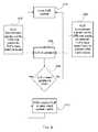
- Function block 402indicates that PCIE Environment 204 signals via CRB 206 that credits for TLPs have been received.
- function block 404indicates that Environment 204 signals via CFB 208 that credits for received TLPs have been freed.
- Environment 204signals that initial credit values have been advertised by a Receiver component.
- Function block 406shows that when either of these events occurs, CSR 216 is updated. Thereupon, CUP 214 must decide whether or not to send an update by means of CUB 210 , as described above. This is indicated by decision block 408 .
- CCE 202goes to a mode of waiting for the next CSR update, as indicated by function block 410 . If the CUP decides to send an update, CCE 202 operates CUB 210 to send the update credits, as shown by function 212 . Thereafter, CCE 202 goes to a mode of waiting for the next CSR update.
Landscapes
- Engineering & Computer Science (AREA)
- General Engineering & Computer Science (AREA)
- Theoretical Computer Science (AREA)
- Computer Hardware Design (AREA)
- Physics & Mathematics (AREA)
- General Physics & Mathematics (AREA)
- Data Exchanges In Wide-Area Networks (AREA)
Abstract
Description
- Header/Data Credit Count for last CUB Completion_Credit_Update_Event
- Header/Data Credit Count for last CUB Posted_Credit_Update_Event
- Header/Data Credit Count for last CUB Non-Posted_Credit_Update_Event
- Header/Data Credit Count for last CRB Completion_Credit_Received_Event
- Header/Data Credit Count for last CRB Posted_Credit_Received_Event
- Header/Data Credit Count for last CRB Non-Posted_Credit_Received_Event
- Header/Data Credit Count for last CFB Completion_Credit_Freed_Event
- Header/Data Credit Count for last CFB Posted_Credit_Freed_Event
- Header/Data Credit Count for last CFB Posted_Credit_Freed_Event
- Running total of Header/Data Credit Counts for all CUB Completion_Credit_Update_Event
- Running total of Header/Data Credit Counts for all CUB Posted_Credit_Update_Event
- Running total of Header/Data Credit Counts for all CUB Non-Posted_Credit_Update_Event
- Running total of Header/Data Credit Counts for all CRB Completion_Credit_Received_Events
- Running total of Header/Data Credit Counts for all CRB Posted_Credit_Received_Event
- Running total of Header/Data Credit Counts for all CRB Non-Posted_Credit_Update_Event
- Running total of Header/Data Credit Counts for all CFB Completion_Credit_Freed_Event
- Running total of Header/Data Credit Counts for all CFB Posted_Credit_Freed_Event
- Running total of Header/Data Credit Counts for all CFB Posted_Credit_Freed_Event
Claims (13)
Priority Applications (1)
| Application Number | Priority Date | Filing Date | Title |
|---|---|---|---|
| US11/290,096US7698477B2 (en) | 2005-11-30 | 2005-11-30 | Method and apparatus for managing flow control in PCI express transaction layer |
Applications Claiming Priority (1)
| Application Number | Priority Date | Filing Date | Title |
|---|---|---|---|
| US11/290,096US7698477B2 (en) | 2005-11-30 | 2005-11-30 | Method and apparatus for managing flow control in PCI express transaction layer |
Publications (2)
| Publication Number | Publication Date |
|---|---|
| US20070121495A1 US20070121495A1 (en) | 2007-05-31 |
| US7698477B2true US7698477B2 (en) | 2010-04-13 |
Family
ID=38087333
Family Applications (1)
| Application Number | Title | Priority Date | Filing Date |
|---|---|---|---|
| US11/290,096Expired - Fee RelatedUS7698477B2 (en) | 2005-11-30 | 2005-11-30 | Method and apparatus for managing flow control in PCI express transaction layer |
Country Status (1)
| Country | Link |
|---|---|
| US (1) | US7698477B2 (en) |
Cited By (10)
| Publication number | Priority date | Publication date | Assignee | Title |
|---|---|---|---|---|
| US20100088554A1 (en)* | 2008-10-08 | 2010-04-08 | Udell John C | Apparatus and methods for capture of flow control errors in clock domain crossing data transfers |
| US7852757B1 (en)* | 2009-03-10 | 2010-12-14 | Xilinx, Inc. | Status based data flow control for chip systems |
| US20110128963A1 (en)* | 2009-11-30 | 2011-06-02 | Nvidia Corproation | System and method for virtual channel communication |
| US8065465B1 (en)* | 2009-06-10 | 2011-11-22 | Nvidia Corporation | Mitigating main crossbar load using dedicated connections for certain traffic types |
| US8295293B1 (en)* | 2009-12-16 | 2012-10-23 | Integrated Device Technology, Inc. | Predictive flow control for a packet switch |
| US8325194B1 (en) | 2009-06-10 | 2012-12-04 | Nvidia Corporation | Mitigating main crossbar load using dedicated connections for certain traffic types |
| US8687639B2 (en) | 2009-06-04 | 2014-04-01 | Nvidia Corporation | Method and system for ordering posted packets and non-posted packets transfer |
| US9331869B2 (en) | 2010-03-04 | 2016-05-03 | Nvidia Corporation | Input/output request packet handling techniques by a device specific kernel mode driver |
| US9367487B1 (en) | 2009-06-10 | 2016-06-14 | Nvidia Corporation | Mitigating main crossbar load using dedicated connections for certain traffic types |
| US11741025B2 (en) | 2020-12-01 | 2023-08-29 | Western Digital Technologies, Inc. | Storage system and method for providing a dual-priority credit system |
Families Citing this family (17)
| Publication number | Priority date | Publication date | Assignee | Title |
|---|---|---|---|---|
| US7694049B2 (en)* | 2005-12-28 | 2010-04-06 | Intel Corporation | Rate control of flow control updates |
| US8194547B1 (en)* | 2006-08-07 | 2012-06-05 | Emc Corporation | Configuring flow control settings |
| US7698478B2 (en)* | 2006-09-19 | 2010-04-13 | Apple Inc. | Managed credit update |
| US8051217B2 (en)* | 2007-01-12 | 2011-11-01 | Dell Products L.P. | System and method for providing PCIe over displayport |
| US8174977B2 (en)* | 2007-07-06 | 2012-05-08 | Hewlett-Packard Development Company, L.P. | End-to-end flow control in a network |
| CN100574310C (en)* | 2007-08-24 | 2009-12-23 | 中国科学院计算技术研究所 | A kind of credit flow control method |
| US7725640B2 (en)* | 2008-04-18 | 2010-05-25 | Lsi Corporation | Adapter card replay buffer for system fault analysis |
| US7562168B1 (en)* | 2008-05-29 | 2009-07-14 | International Business Machines Corporation | Method of optimizing buffer usage of virtual channels of a physical communication link and apparatuses for performing the same |
| US8045472B2 (en)* | 2008-12-29 | 2011-10-25 | Apple Inc. | Credit management when resource granularity is larger than credit granularity |
| US9524261B2 (en) | 2012-12-21 | 2016-12-20 | Apple Inc. | Credit lookahead mechanism |
| US10061734B2 (en) | 2015-05-20 | 2018-08-28 | International Business Machines Corporation | Adjustment of buffer credits and other parameters in a startup phase of communications between a plurality of channels and a control unit |
| US9892065B2 (en)* | 2015-05-20 | 2018-02-13 | International Business Machines Corporation | Adjustments of buffer credits for optimizing the number of retry operations and transfer ready operations |
| US9864716B2 (en)* | 2015-05-20 | 2018-01-09 | International Business Machines Corporation | Receiving buffer credits by a plurality of channels of one or more host computational devices for transmitting data to a control unit |
| WO2019036217A1 (en) | 2017-08-18 | 2019-02-21 | Missing Link Electronics, Inc. | Heterogeneous packet-based transport |
| US11356388B2 (en) | 2017-08-18 | 2022-06-07 | Missing Link Electronics, Inc. | Real-time multi-protocol heterogeneous packet-based transport |
| US10469395B2 (en) | 2017-08-31 | 2019-11-05 | Hewlett Packard Enterprise Development Lp | Packet transmission credit allocation |
| CN119996314B (en)* | 2025-04-16 | 2025-07-25 | 北京诺芮集成电路设计有限公司 | PCIe data packet sending method, electronic device and medium |
Citations (8)
| Publication number | Priority date | Publication date | Assignee | Title |
|---|---|---|---|---|
| US6747949B1 (en)* | 1999-05-21 | 2004-06-08 | Intel Corporation | Register based remote data flow control |
| US6874054B2 (en)* | 2002-12-19 | 2005-03-29 | Emulex Design & Manufacturing Corporation | Direct memory access controller system with message-based programming |
| US20050259651A1 (en)* | 2004-05-20 | 2005-11-24 | Kabushiki Kaisha Toshiba | Data processing apparatus and flow control method |
| US20070133415A1 (en)* | 2005-12-13 | 2007-06-14 | Intel Corporation | Method and apparatus for flow control initialization |
| US7266083B2 (en)* | 2003-02-26 | 2007-09-04 | International Business Machines Corporation | Method and apparatus for implementing queue pair connection protection over infiniband |
| US7406092B2 (en)* | 2003-07-21 | 2008-07-29 | Qlogic, Corporation | Programmable pseudo virtual lanes for fibre channel systems |
| US7480293B2 (en)* | 2004-02-05 | 2009-01-20 | Qlogic, Corporation | Method and system for preventing deadlock in fibre channel fabrics using frame priorities |
| US7512067B2 (en)* | 2003-07-21 | 2009-03-31 | Qlogic, Corporation | Method and system for congestion control based on optimum bandwidth allocation in a fibre channel switch |
- 2005
- 2005-11-30USUS11/290,096patent/US7698477B2/ennot_activeExpired - Fee Related
Patent Citations (8)
| Publication number | Priority date | Publication date | Assignee | Title |
|---|---|---|---|---|
| US6747949B1 (en)* | 1999-05-21 | 2004-06-08 | Intel Corporation | Register based remote data flow control |
| US6874054B2 (en)* | 2002-12-19 | 2005-03-29 | Emulex Design & Manufacturing Corporation | Direct memory access controller system with message-based programming |
| US7266083B2 (en)* | 2003-02-26 | 2007-09-04 | International Business Machines Corporation | Method and apparatus for implementing queue pair connection protection over infiniband |
| US7406092B2 (en)* | 2003-07-21 | 2008-07-29 | Qlogic, Corporation | Programmable pseudo virtual lanes for fibre channel systems |
| US7512067B2 (en)* | 2003-07-21 | 2009-03-31 | Qlogic, Corporation | Method and system for congestion control based on optimum bandwidth allocation in a fibre channel switch |
| US7480293B2 (en)* | 2004-02-05 | 2009-01-20 | Qlogic, Corporation | Method and system for preventing deadlock in fibre channel fabrics using frame priorities |
| US20050259651A1 (en)* | 2004-05-20 | 2005-11-24 | Kabushiki Kaisha Toshiba | Data processing apparatus and flow control method |
| US20070133415A1 (en)* | 2005-12-13 | 2007-06-14 | Intel Corporation | Method and apparatus for flow control initialization |
Cited By (12)
| Publication number | Priority date | Publication date | Assignee | Title |
|---|---|---|---|---|
| US20100088554A1 (en)* | 2008-10-08 | 2010-04-08 | Udell John C | Apparatus and methods for capture of flow control errors in clock domain crossing data transfers |
| US7913124B2 (en)* | 2008-10-08 | 2011-03-22 | Lsi Corporation | Apparatus and methods for capture of flow control errors in clock domain crossing data transfers |
| US7852757B1 (en)* | 2009-03-10 | 2010-12-14 | Xilinx, Inc. | Status based data flow control for chip systems |
| US8687639B2 (en) | 2009-06-04 | 2014-04-01 | Nvidia Corporation | Method and system for ordering posted packets and non-posted packets transfer |
| US8065465B1 (en)* | 2009-06-10 | 2011-11-22 | Nvidia Corporation | Mitigating main crossbar load using dedicated connections for certain traffic types |
| US8325194B1 (en) | 2009-06-10 | 2012-12-04 | Nvidia Corporation | Mitigating main crossbar load using dedicated connections for certain traffic types |
| US9367487B1 (en) | 2009-06-10 | 2016-06-14 | Nvidia Corporation | Mitigating main crossbar load using dedicated connections for certain traffic types |
| US20110128963A1 (en)* | 2009-11-30 | 2011-06-02 | Nvidia Corproation | System and method for virtual channel communication |
| US8532098B2 (en)* | 2009-11-30 | 2013-09-10 | Nvidia Corporation | System and method for virtual channel communication |
| US8295293B1 (en)* | 2009-12-16 | 2012-10-23 | Integrated Device Technology, Inc. | Predictive flow control for a packet switch |
| US9331869B2 (en) | 2010-03-04 | 2016-05-03 | Nvidia Corporation | Input/output request packet handling techniques by a device specific kernel mode driver |
| US11741025B2 (en) | 2020-12-01 | 2023-08-29 | Western Digital Technologies, Inc. | Storage system and method for providing a dual-priority credit system |
Also Published As
| Publication number | Publication date |
|---|---|
| US20070121495A1 (en) | 2007-05-31 |
Similar Documents
| Publication | Publication Date | Title |
|---|---|---|
| US7698477B2 (en) | Method and apparatus for managing flow control in PCI express transaction layer | |
| US7660917B2 (en) | System and method of implementing multiple internal virtual channels based on a single external virtual channel | |
| US6425021B1 (en) | System for transferring data packets of different context utilizing single interface and concurrently processing data packets of different contexts | |
| US8856340B2 (en) | Multi-adapter link aggregation for adapters with hardware based virtual bridges | |
| US9652426B2 (en) | Method, device, system and storage medium for implementing packet transmission in PCIE switching network | |
| EP1374521B1 (en) | Method and apparatus for remote key validation for ngio/infiniband applications | |
| US7827325B2 (en) | Device, system, and method of speculative packet transmission | |
| US9253287B2 (en) | Speculation based approach for reliable message communications | |
| EP1591908A1 (en) | Separating transactions into different virtual channels | |
| US20080288664A1 (en) | Switching apparatus and method for link initialization in a shared i/o environment | |
| CN101102305A (en) | System and method for managing network information processing | |
| JP2006189937A (en) | Receiving device, transmitting / receiving device, receiving method, and transmitting / receiving method | |
| US7460531B2 (en) | Method, system, and program for constructing a packet | |
| US7028130B2 (en) | Generating multiple traffic classes on a PCI Express fabric from PCI devices | |
| US7424567B2 (en) | Method, system, and apparatus for a dynamic retry buffer that holds a packet for transmission | |
| US20080215926A1 (en) | Dubug by a Communication Device | |
| US6816889B1 (en) | Assignment of dual port memory banks for a CPU and a host channel adapter in an InfiniBand computing node | |
| US20040019704A1 (en) | Multiple processor integrated circuit having configurable packet-based interfaces | |
| US11593281B2 (en) | Device supporting ordered and unordered transaction classes | |
| US7346078B2 (en) | Processing of received data within a multiple processor device | |
| US20040151175A1 (en) | Transparent data format within host device supporting differing transaction types | |
| JP4432388B2 (en) | Input/Output Control Unit | |
| US7380030B2 (en) | Method and system for using an in-line credit extender with a host bus adapter | |
| US20250103090A1 (en) | Devices, systems, and methods for dynamically changing frequencies of clocks for the data link layer without downtime | |
| WO2024102916A1 (en) | Root complex switching across inter-die data interface to multiple endpoints |
Legal Events
| Date | Code | Title | Description |
|---|---|---|---|
| AS | Assignment | Owner name:LSI LOGIC CORPORATION,CALIFORNIA Free format text:ASSIGNMENT OF ASSIGNORS INTEREST;ASSIGNORS:BRETI, JEFFREY WILLIAM;SANDERS, DOUGLAS ELLIOTT;BHARADWAJ, HARISH;AND OTHERS;SIGNING DATES FROM 20051121 TO 20051128;REEL/FRAME:017462/0688 Owner name:LSI LOGIC CORPORATION, CALIFORNIA Free format text:ASSIGNMENT OF ASSIGNORS INTEREST;ASSIGNORS:BRETI, JEFFREY WILLIAM;SANDERS, DOUGLAS ELLIOTT;BHARADWAJ, HARISH;AND OTHERS;REEL/FRAME:017462/0688;SIGNING DATES FROM 20051121 TO 20051128 | |
| FEPP | Fee payment procedure | Free format text:PAYOR NUMBER ASSIGNED (ORIGINAL EVENT CODE: ASPN); ENTITY STATUS OF PATENT OWNER: LARGE ENTITY | |
| FEPP | Fee payment procedure | Free format text:PAYER NUMBER DE-ASSIGNED (ORIGINAL EVENT CODE: RMPN); ENTITY STATUS OF PATENT OWNER: LARGE ENTITY Free format text:PAYOR NUMBER ASSIGNED (ORIGINAL EVENT CODE: ASPN); ENTITY STATUS OF PATENT OWNER: LARGE ENTITY | |
| STCF | Information on status: patent grant | Free format text:PATENTED CASE | |
| FPAY | Fee payment | Year of fee payment:4 | |
| AS | Assignment | Owner name:DEUTSCHE BANK AG NEW YORK BRANCH, AS COLLATERAL AG Free format text:PATENT SECURITY AGREEMENT;ASSIGNORS:LSI CORPORATION;AGERE SYSTEMS LLC;REEL/FRAME:032856/0031 Effective date:20140506 | |
| AS | Assignment | Owner name:LSI CORPORATION, CALIFORNIA Free format text:CHANGE OF NAME;ASSIGNOR:LSI LOGIC CORPORATION;REEL/FRAME:033102/0270 Effective date:20070406 | |
| AS | Assignment | Owner name:AVAGO TECHNOLOGIES GENERAL IP (SINGAPORE) PTE. LTD Free format text:ASSIGNMENT OF ASSIGNORS INTEREST;ASSIGNOR:LSI CORPORATION;REEL/FRAME:035390/0388 Effective date:20140814 | |
| AS | Assignment | Owner name:AGERE SYSTEMS LLC, PENNSYLVANIA Free format text:TERMINATION AND RELEASE OF SECURITY INTEREST IN PATENT RIGHTS (RELEASES RF 032856-0031);ASSIGNOR:DEUTSCHE BANK AG NEW YORK BRANCH, AS COLLATERAL AGENT;REEL/FRAME:037684/0039 Effective date:20160201 Owner name:LSI CORPORATION, CALIFORNIA Free format text:TERMINATION AND RELEASE OF SECURITY INTEREST IN PATENT RIGHTS (RELEASES RF 032856-0031);ASSIGNOR:DEUTSCHE BANK AG NEW YORK BRANCH, AS COLLATERAL AGENT;REEL/FRAME:037684/0039 Effective date:20160201 | |
| AS | Assignment | Owner name:BANK OF AMERICA, N.A., AS COLLATERAL AGENT, NORTH CAROLINA Free format text:PATENT SECURITY AGREEMENT;ASSIGNOR:AVAGO TECHNOLOGIES GENERAL IP (SINGAPORE) PTE. LTD.;REEL/FRAME:037808/0001 Effective date:20160201 Owner name:BANK OF AMERICA, N.A., AS COLLATERAL AGENT, NORTH Free format text:PATENT SECURITY AGREEMENT;ASSIGNOR:AVAGO TECHNOLOGIES GENERAL IP (SINGAPORE) PTE. LTD.;REEL/FRAME:037808/0001 Effective date:20160201 | |
| AS | Assignment | Owner name:AVAGO TECHNOLOGIES GENERAL IP (SINGAPORE) PTE. LTD., SINGAPORE Free format text:TERMINATION AND RELEASE OF SECURITY INTEREST IN PATENTS;ASSIGNOR:BANK OF AMERICA, N.A., AS COLLATERAL AGENT;REEL/FRAME:041710/0001 Effective date:20170119 Owner name:AVAGO TECHNOLOGIES GENERAL IP (SINGAPORE) PTE. LTD Free format text:TERMINATION AND RELEASE OF SECURITY INTEREST IN PATENTS;ASSIGNOR:BANK OF AMERICA, N.A., AS COLLATERAL AGENT;REEL/FRAME:041710/0001 Effective date:20170119 | |
| MAFP | Maintenance fee payment | Free format text:PAYMENT OF MAINTENANCE FEE, 8TH YEAR, LARGE ENTITY (ORIGINAL EVENT CODE: M1552) Year of fee payment:8 | |
| AS | Assignment | Owner name:AVAGO TECHNOLOGIES INTERNATIONAL SALES PTE. LIMITE Free format text:MERGER;ASSIGNOR:AVAGO TECHNOLOGIES GENERAL IP (SINGAPORE) PTE. LTD.;REEL/FRAME:047196/0687 Effective date:20180509 | |
| AS | Assignment | Owner name:AVAGO TECHNOLOGIES INTERNATIONAL SALES PTE. LIMITE Free format text:CORRECTIVE ASSIGNMENT TO CORRECT THE EFFECTIVE DATE OF MERGER TO 9/5/2018 PREVIOUSLY RECORDED AT REEL: 047196 FRAME: 0687. ASSIGNOR(S) HEREBY CONFIRMS THE MERGER;ASSIGNOR:AVAGO TECHNOLOGIES GENERAL IP (SINGAPORE) PTE. LTD.;REEL/FRAME:047630/0344 Effective date:20180905 | |
| AS | Assignment | Owner name:AVAGO TECHNOLOGIES INTERNATIONAL SALES PTE. LIMITE Free format text:CORRECTIVE ASSIGNMENT TO CORRECT THE PROPERTY NUMBERS PREVIOUSLY RECORDED AT REEL: 47630 FRAME: 344. ASSIGNOR(S) HEREBY CONFIRMS THE ASSIGNMENT;ASSIGNOR:AVAGO TECHNOLOGIES GENERAL IP (SINGAPORE) PTE. LTD.;REEL/FRAME:048883/0267 Effective date:20180905 | |
| FEPP | Fee payment procedure | Free format text:MAINTENANCE FEE REMINDER MAILED (ORIGINAL EVENT CODE: REM.); ENTITY STATUS OF PATENT OWNER: LARGE ENTITY | |
| LAPS | Lapse for failure to pay maintenance fees | Free format text:PATENT EXPIRED FOR FAILURE TO PAY MAINTENANCE FEES (ORIGINAL EVENT CODE: EXP.); ENTITY STATUS OF PATENT OWNER: LARGE ENTITY | |
| STCH | Information on status: patent discontinuation | Free format text:PATENT EXPIRED DUE TO NONPAYMENT OF MAINTENANCE FEES UNDER 37 CFR 1.362 | |
| FP | Lapsed due to failure to pay maintenance fee | Effective date:20220413 |