US7697326B2 - Reducing programming error in memory devices - Google Patents
Reducing programming error in memory devicesDownload PDFInfo
- Publication number
- US7697326B2 US7697326B2US11/995,806US99580607AUS7697326B2US 7697326 B2US7697326 B2US 7697326B2US 99580607 AUS99580607 AUS 99580607AUS 7697326 B2US7697326 B2US 7697326B2
- Authority
- US
- United States
- Prior art keywords
- voltage
- memory cells
- data
- analog memory
- voltage levels
- Prior art date
- Legal status (The legal status is an assumption and is not a legal conclusion. Google has not performed a legal analysis and makes no representation as to the accuracy of the status listed.)
- Expired - Fee Related
Links
- 230000015654memoryEffects0.000claimsabstractdescription187
- 238000000034methodMethods0.000claimsabstractdescription72
- 238000012986modificationMethods0.000claimsabstractdescription16
- 230000004048modificationEffects0.000claimsabstractdescription16
- 238000012545processingMethods0.000claimsdescription55
- 238000012937correctionMethods0.000claimsdescription26
- 239000011159matrix materialSubstances0.000claimsdescription11
- 230000001965increasing effectEffects0.000claimsdescription8
- 230000008859changeEffects0.000claimsdescription6
- 230000006870functionEffects0.000claimsdescription5
- 150000004767nitridesChemical class0.000claimsdescription4
- 238000005192partitionMethods0.000claimsdescription2
- 238000000638solvent extractionMethods0.000claimsdescription2
- 210000004027cellAnatomy0.000description213
- 239000000872bufferSubstances0.000description13
- 230000008569processEffects0.000description11
- 238000009826distributionMethods0.000description5
- 230000007246mechanismEffects0.000description5
- 238000010586diagramMethods0.000description4
- 230000003044adaptive effectEffects0.000description3
- 230000008878couplingEffects0.000description3
- 238000010168coupling processMethods0.000description3
- 238000005859coupling reactionMethods0.000description3
- 238000007726management methodMethods0.000description3
- 238000012795verificationMethods0.000description3
- 230000032683agingEffects0.000description2
- 238000013459approachMethods0.000description2
- 230000008901benefitEffects0.000description2
- 238000004891communicationMethods0.000description2
- 230000005684electric fieldEffects0.000description2
- 230000002708enhancing effectEffects0.000description2
- LZIAMMQBHJIZAG-UHFFFAOYSA-N2-[di(propan-2-yl)amino]ethyl carbamimidothioateChemical compoundCC(C)N(C(C)C)CCSC(N)=NLZIAMMQBHJIZAG-UHFFFAOYSA-N0.000description1
- 238000003491arrayMethods0.000description1
- 230000001413cellular effectEffects0.000description1
- 238000006243chemical reactionMethods0.000description1
- 230000000295complement effectEffects0.000description1
- 238000012885constant functionMethods0.000description1
- 238000013500data storageMethods0.000description1
- 238000013461designMethods0.000description1
- 238000001514detection methodMethods0.000description1
- 238000005315distribution functionMethods0.000description1
- 230000000694effectsEffects0.000description1
- 239000000284extractSubstances0.000description1
- 239000000543intermediateSubstances0.000description1
- 238000005259measurementMethods0.000description1
- 229910044991metal oxideInorganic materials0.000description1
- 150000004706metal oxidesChemical class0.000description1
- 230000002265preventionEffects0.000description1
- 230000004044responseEffects0.000description1
- 239000004065semiconductorSubstances0.000description1
- 238000012163sequencing techniqueMethods0.000description1
- 239000007787solidSubstances0.000description1
- 210000000352storage cellAnatomy0.000description1
Images


Classifications
- G—PHYSICS
- G11—INFORMATION STORAGE
- G11C—STATIC STORES
- G11C11/00—Digital stores characterised by the use of particular electric or magnetic storage elements; Storage elements therefor
- G11C11/56—Digital stores characterised by the use of particular electric or magnetic storage elements; Storage elements therefor using storage elements with more than two stable states represented by steps, e.g. of voltage, current, phase, frequency
- G11C11/5621—Digital stores characterised by the use of particular electric or magnetic storage elements; Storage elements therefor using storage elements with more than two stable states represented by steps, e.g. of voltage, current, phase, frequency using charge storage in a floating gate
- G11C11/5628—Programming or writing circuits; Data input circuits
- G—PHYSICS
- G11—INFORMATION STORAGE
- G11C—STATIC STORES
- G11C2211/00—Indexing scheme relating to digital stores characterized by the use of particular electric or magnetic storage elements; Storage elements therefor
- G11C2211/56—Indexing scheme relating to G11C11/56 and sub-groups for features not covered by these groups
- G11C2211/562—Multilevel memory programming aspects
- G11C2211/5621—Multilevel programming verification
- G—PHYSICS
- G11—INFORMATION STORAGE
- G11C—STATIC STORES
- G11C27/00—Electric analogue stores, e.g. for storing instantaneous values
- G11C27/005—Electric analogue stores, e.g. for storing instantaneous values with non-volatile charge storage, e.g. on floating gate or MNOS
- H—ELECTRICITY
- H04—ELECTRIC COMMUNICATION TECHNIQUE
- H04Q—SELECTING
- H04Q2213/00—Indexing scheme relating to selecting arrangements in general and for multiplex systems
- H04Q2213/13103—Memory
- H—ELECTRICITY
- H04—ELECTRIC COMMUNICATION TECHNIQUE
- H04Q—SELECTING
- H04Q2213/00—Indexing scheme relating to selecting arrangements in general and for multiplex systems
- H04Q2213/13106—Microprocessor, CPU
- H—ELECTRICITY
- H04—ELECTRIC COMMUNICATION TECHNIQUE
- H04Q—SELECTING
- H04Q2213/00—Indexing scheme relating to selecting arrangements in general and for multiplex systems
- H04Q2213/13305—Transistors, semiconductors in general
- H—ELECTRICITY
- H04—ELECTRIC COMMUNICATION TECHNIQUE
- H04Q—SELECTING
- H04Q2213/00—Indexing scheme relating to selecting arrangements in general and for multiplex systems
- H04Q2213/1332—Logic circuits
Definitions
- the present inventionrelates generally to memory devices, and specifically to methods and devices for reducing errors in data storage and readout.
- Flash memory devicessuch as Flash memories and Dynamic Random Access Memory (DRAM), use arrays of analog memory cells for storing data. Flash memory devices are described, for example, by Bez et al., in “Introduction to Flash Memory,” Proceedings of the IEEE 91:4 (April, 2003), pages 489-502, which is incorporated herein by reference.
- each analog memory celltypically comprises a transistor, which holds a certain amount of electric charge that represents the information stored in the cell. The electric charge written into a particular cell influences the “threshold voltage” of the cell, i.e., the voltage that needs to be applied to the cell so that the cell will conduct current.
- Some memory devicescommonly referred to as Single-Level Cell (SLC) devices, store a single bit of information in each memory cell.
- SLCSingle-Level Cell
- the range of possible threshold voltages of the cellis divided into two regions. A voltage value falling in one of the regions represents a “0” bit value, and a voltage belonging to the second region represents “1”.
- Higher-density devicesoften referred to as Multi-Level Cell (MLC) devices, store more than one bit per memory cell.
- MLCMulti-Level Cell
- the range of threshold voltagesis divided into more than two regions, with each region representing more than one bit.
- Multi-level Flash cells and devicesare described, for example, by Eitan et al., in “Multilevel Flash Cells and their Trade-Offs,” Proceedings of the 1996 IEEE International Electron Devices Meeting ( IEDM ) (New York, N.Y.), pages 169-172, which is incorporated herein by reference.
- the papercompares several kinds of multilevel Flash cells, such as common ground, DINOR, AND, NOR and NAND cells.
- Other types of analog memory cellsthat are known in the art include Nitride Read Only Memory (NROM), Ferroelectric RAM (FRAM), Magnetic RAM (MRAM) and Phase change RAM (PRAM, also referred to as Phase Change Memory—PCM).
- the data stored in the memory deviceis encoded using an Error Correcting Code (ECC).
- ECCError Correcting Code
- Rodney and Sayanodescribe a number of on-chip coding techniques for the protection of Random Access Memory (RAM) devices, which use multi-level storage cells, in “On-Chip ECC for Multi-Level Random Access Memories,” Proceedings of the 1989 IEEE/CAM Information Theory Workshop (Jun. 25-29, 1989, Ithaca, N.Y.), which is incorporated herein by reference.
- U.S. Pat. No. 6,212,654whose disclosure is incorporated herein by reference, describes methods for storing data in an analog memory device using coded modulation techniques.
- Other ECC schemes for multilevel memory devicesare described in U.S. Pat. Nos. 6,469,931 and 7,023,735, whose disclosures are incorporated herein by reference.
- the threshold voltage values read from analog memory cellsare sometimes distorted.
- the distortionmay be due to various causes, such as electrical field coupling from neighboring memory cells, disturb noise caused by operations on other cells in the array, and threshold voltage drift caused by device aging.
- Some common distortion mechanismsare described in the article by Bez et al., cited above.
- U.S. Pat. No. 5,867,429whose disclosure is incorporated herein by reference, describes a method for compensating for electric field coupling between floating gates of a high-density Flash Electrically Erasable Programmable Read Only Memory (EEPROM) cell array.
- EEPROMElectrically Erasable Programmable Read Only Memory
- Embodiments of the present inventionprovide a method for storing data in an array of analog memory cells.
- the methodincludes defining a constellation of voltage levels to be used in storing the data in the analog memory cells, and writing a part of the data to a first analog memory cell in the array by applying to the analog memory cell a first voltage level selected from the constellation. After writing the part of the data to the first analog memory cell, a second voltage level that does not belong to the constellation is read from the first analog memory cell. A modification to be made in writing to one or more of the analog memory cells in the array is determined responsively to the second voltage level. Data are written to the one or more of the analog memory cells subject to the modification.
- determining the modificationincludes selecting one or more third voltage levels to be written respectively to one or more of the analog memory cells, and writing to the one or more of the analog memory cells includes writing the one or more third voltage levels to the one or more of the analog memory cells.
- selecting the one or more third voltage levelsincludes determining a voltage correction to be applied to the first analog memory cell, and writing the one or more third voltage levels includes adding charge to the first analog memory cell so as to apply the voltage correction.
- defining the constellationincludes defining a matrix of codewords to represent the data, each codeword corresponding to a set of the voltage levels in the constellation that are to be written to a corresponding set of the analog memory cells, and determining the voltage correction includes finding a distance between the set of the voltage levels, including the second voltage level, read from the corresponding set of the analog memory cells and one of the codewords in the matrix, and choosing the voltage correction so as to reduce the distance.
- Writing the part of the datamay include choosing a first codeword in the matrix to be written to the corresponding set of the analog memory cells, and finding the distance may include determining a first distance between the set of the voltage levels and the first codeword and a second distance between the set of the voltage levels and a second codeword in proximity to the first codeword, whereupon choosing the voltage correction includes computing the voltage correction so as to reduce a ratio of the first distance to the second distance.
- the methodmay include, when the distance exceeds a maximal distance criterion, rewriting the part of the data to the first analog memory cell.
- selecting the one or more third voltage levelsincludes selecting a third voltage level from the constellation to be written to a second analog memory cell.
- selecting the third voltage levelincludes choosing the third voltage level responsively to both the first voltage level and the second voltage level, while applying feedback coding so as to write multiple successive voltage levels representing the data to a succession of the analog memory cells.
- Applying the feedback codingmay include choosing the first voltage level responsively to a probability density function (PDF), which relates the data to the voltage levels that are to be used in storing the data in the analog memory cells, and choosing the third voltage level may include updating the PDF responsively to the first and second voltage levels, and choosing the third voltage level responsively to the updated PDF.
- PDFprobability density function
- choosing the third voltage levelmay include partitioning the PDF into 2 M sub-intervals corresponding to the 2 M voltage levels, selecting one of the sub-intervals responsively to a value of the data, and choosing the third voltage level that corresponds to the selected one of the sub-intervals.
- writing the part of the datamay include writing respective first voltage levels to a first group of the memory cells in a first row in the array, wherein the second analog memory cell belongs to a second group of the memory cells in a second row of the array, to which the one or more third voltage levels are written after writing to the memory cells in the first row, and wherein each of the memory cells is located in a respective column, and selecting the third voltage level includes determining a respective third voltage level to write to each of the memory cells in the second group responsively to the second voltage level read from one of the first group of the memory cells in the same respective column.
- writing the part of the datamay include simultaneously writing respective first voltage levels to a first group of the memory cells in a first row in the array, wherein the first and second analog memory cells are chosen from among the memory cells in the group responsively to an ordering of the voltage levels to be written to the memory cells.
- the constellationhas a first voltage resolution
- reading the second voltage levelincludes determining the second voltage level with a second voltage resolution that is finer than the first voltage resolution.
- the memory cellsare selected from a set of memory cell types consisting of Flash memory cells, Dynamic Random Access Memory (DRAM) cells, Phase Change Memory (PCM) cells, Nitride Read-Only Memory (NROM) cells, and Magnetic Random Access Memory (MRAM) cells.
- DRAMDynamic Random Access Memory
- PCMPhase Change Memory
- NROMNitride Read-Only Memory
- MRAMMagnetic Random Access Memory
- the constellation of the voltage levelsincludes at least four voltage levels per cell.
- the constellationis modified responsively to the second voltage level. In one embodiment, modifying the constellation includes increasing at least one of the voltage levels to be used in storing the data.
- the modificationincludes changing a number of error correction bits that are to be added to a word of the data.
- apparatus for storing dataincluding:
- a read/write unitwhich is coupled to an array of analog memory cells so as to write a part of the data to a first analog memory cell in the array by applying to the analog memory cell a first voltage level selected from a predefined constellation of voltage levels, and which is configured to read from the first analog memory cell, after writing the part of the data thereto, a second voltage level that does not belong to the constellation;
- a signal processing unitwhich is configured to determine, responsively to the second voltage level, a modification to be made in writing to one or more of the analog memory cells in the array, and to instruct the read/write unit to write to the one or more of the analog memory cells subject to the modification.
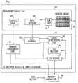
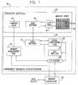
- FIG. 1is a block diagram that schematically illustrates a memory system, in accordance with an embodiment of the present invention
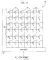
- FIG. 2is a schematic circuit diagram that illustrates a memory cell array, in accordance with an embodiment of the present invention
- FIG. 3is a schematic plot of voltage distribution in an array of multi-level memory cells, in accordance with an embodiment of the present invention.
- FIG. 4is a schematic plot of constellation points and voltage values used in programming a memory device with encoded data, in accordance with an embodiment of the present invention
- FIG. 5is a flow chart that schematically illustrates a method for programming a memory device, in accordance with an embodiment of the present invention.
- FIG. 6is a flow chart that schematically illustrates a method for programming a memory device, in accordance with another embodiment of the present invention.
- Some analog memory devicesuse a process of “program and verify” (P&V) in writing information to the memory cells.
- P&Vprogram and verify
- a cellis programmed by applying a sequence of voltage pulses, whose voltage level increases from pulse to pulse.
- the programmed voltage levelis read (“verified”) after each pulse, and the iterations continue until the desired level is reached.
- the embodiments of the present invention that are described hereinbelowimprove upon the conventional program-and-verify model by measuring the voltages of analog memory cells against a set of levels that are different from the constellation of levels that correspond to the data values that may be written to the cells.
- the set of levels used in measuring the cell voltageshas finer resolution, i.e., is more tightly spaced, than the set of levels in the write constellation.
- the measured voltage levelsmay then be used, for example, in providing fine correction to the amount of charge already stored in the cells, or in a feedback coding scheme for determining the voltage levels to be used in writing to subsequent cells in the array.
- FIG. 1is a block diagram that schematically illustrates a memory system 20 , in accordance with an embodiment of the present invention.
- System 20can be used in various host systems and devices, such as in computing devices, cellular phones or other communication terminals, removable memory modules (such as “disk-on-key” devices), digital cameras, music and other media players and/or any other system or device in which data is stored and retrieved.
- memory system 20interacts with a memory controller 22 , i.e., accepts data for storage from the memory controller and outputs data that are stored in memory to the memory controller when requested.
- System 20comprises a memory device 24 , which stores data in a memory cell array 28 .
- the memory arraycomprises multiple analog memory cells 32 .
- analog memory cellis used to describe any memory cell that holds a continuous, analog value of a physical parameter, such as an electrical voltage or charge.
- Array 28may comprise analog memory cells of any kind, such as, for example, NAND or NOR Flash cells, or PCM, NROM, FRAM, MRAM or DRAM cells.
- the charge levels stored in the cells and/or the analog voltages written into and read out of the cellsare referred to herein collectively as analog values.
- Data for storage in memory device 24are provided to the device and cached in data buffers 36 .
- the dataare then converted to analog voltages and written into memory cells 32 using a reading/writing (R/W) unit 40 , whose functionality is described in greater detail below.
- R/Wreading/writing
- unit 40converts the electric charge, and thus the analog voltages, of memory cells 32 , into digital samples.
- the samplesare cached in buffers 36 .
- the samples produced by unit 40are referred to as soft samples.
- the operation and timing of memory device 24are managed by control logic 48 .
- MSP 52Memory Signal Processor 52 .
- MSP 52intermediates between memory device 24 and memory controller 22 or other host.
- MSP 52applies novel methods in determining the analog values that are to be written to memory array 28 in order to improve the reliability and storage density of the data.
- MSP 52comprises an encoder/decoder 64 , which typically encodes the data to be written to device 24 using an error correcting code (ECC), and decodes the ECC when reading data out of device 24 .
- a signal processing unit 60processes the data that are written into and retrieved from device 24 .
- unit 60receives digital samples that are indicative of the measured voltage levels of the cells, and then determines further voltage levels to be written (to the same cells and/or other cells) on this basis. Techniques that may be used by unit 60 for this purpose are described in detail hereinbelow with reference to FIGS. 4-6 . Alternatively or additionally, these techniques may be implemented, mutatis mutandis, in the circuitry of memory device 24 , and specifically in R/W unit 40 .
- MSP 52comprises a data buffer 72 , which is used by unit 60 for storing data and for interfacing with memory device 24 .
- MSP 52also comprises an Input/Output (I/O) buffer 56 , which forms an interface between the MSP and the host.
- a memory management unit 76manages the operation and timing of MSP 52 .
- Signal processing unit 60 and management unit 76may be implemented in hardware.
- unit 60 and/or unit 76may comprise microprocessors that run suitable software, or a combination of hardware and software elements.
- memory controller 22 or even a host processormay be configured to carry out some or all of the functions of the signal processing and management units that are described hereinbelow, as well as other functions of MSP 52 .
- FIG. 1is an exemplary system configuration, which is shown purely for the sake of conceptual clarity. Any other suitable configuration can also be used. Elements that are not necessary for understanding the principles of the present invention, such as various interfaces, addressing circuits, timing and sequencing circuits, data scrambling circuits and debugging circuits, have been omitted from the figure for clarity.
- memory device 24 and MSP 52are implemented as two separate Integrated Circuits (ICs). In alternative embodiments, however, the memory device and MSP may be integrated in a single IC or System on Chip (SoC). In some implementations, a single MSP 52 may be connected to multiple memory devices 24 . Additional architectural and functional aspects of system 20 and other possible embodiments of the present invention are described in greater detail in U.S. Provisional Patent Application 60/867,399 and in a PCT patent application entitled, “Combined Distortion Estimation and Error Correction Coding for Memory Devices,” filed on even date, both of which are incorporated herein by reference.
- data to be written into memory device 24are accepted from the host and cached in I/O buffer 56 .
- Encoder/decoder 64encodes the data, and the encoded data are transferred, via data buffers 72 , to memory device 24 .
- the dataare temporarily stored in buffers 36 .
- R/W unit 40converts the data to analog voltage values and writes the data (as analog voltage values) into the appropriate cells 32 of array 28 .
- R/W unit 40reads the analog voltage values from the cell(s) and converts the voltages to soft digital samples.
- the samplesare cached in buffers 36 and transferred to buffers 72 of MSP 52 .
- Signal processing unit 60processes the data samples, using methods that are described hereinbelow, in order to determine data values to be written subsequently by R/W unit.
- R/W unit 40When data are to be read out of system 20 to controller 22 , R/W unit 40 reads the analog voltage values from the appropriate cells and converts these voltage values to digital samples in buffers 36 . Blocks of data are transferred from buffers 72 to unit 60 , and encoder/decoder 64 decodes the ECC of these blocks. Encoder/decoder 64 may use distortion estimation provided by unit 60 to improve the performance of the ECC decoding process (as described in the above-mentioned PCT patent application). The decoded data are transferred via I/O buffer 56 to the memory controller or host.
- FIG. 2is a diagram that schematically illustrates memory cell array 28 , in accordance with an embodiment of the present invention.
- cells 32 in FIG. 2represent Flash memory cells, which are connected in a particular array configuration, the principles of the present invention are applicable to other types of memory cells and other array configurations, as well.
- Some exemplary cell types and array configurations that may be used in this contextare described in the references cited in the Background section above.
- Memory cells 32 of array 28are arranged in a grid having multiple rows and columns.
- Each cell 32comprises a floating-gate Metal-Oxide Semiconductor (MOS) transistor.
- MOSMetal-Oxide Semiconductor
- a certain amount of electrical charge (electrons or holes)can be stored in a particular cell by applying appropriate voltage levels to the transistor gate, source and drain.
- the value stored in the cellcan be read by measuring the threshold voltage of the cell, which is defined as the minimal voltage that must be applied to the gate of the transistor in order to cause the transistor to conduct.
- the read threshold voltageis indicative of the charge stored in the cell.
- the gates of the transistors in each roware connected by word lines 80 .
- the sources of the transistors in each columnare connected by bit lines 84 .
- the sourcesare connected to the bit lines directly.
- the bit linesare connected to strings of floating-gate cells.
- R/W unit 40reads the threshold voltage of a particular cell 32 by applying varying voltage levels to its gate (i.e., to the word line to which the cell is connected) and checking whether the drain current of the cell exceeds a certain threshold (i.e., whether the transistor conducts).
- Unit 40usually applies a sequence of different voltage values to the word line to which the cell is connected, and determines the lowest gate voltage value for which the drain current exceeds the threshold.
- Unit 40then outputs a digital sample to data buffers 36 corresponding to this gate voltage, thus indicating the voltage level of the cell.
- unit 40reads an entire row of cells, also referred to as a page, simultaneously. Alternatively, unit 40 may read cells individually.
- unit 40measures the drain current by pre-charging the bit line of the cell to a certain voltage level. Once the gate voltage is set to the desired value, the drain current causes the bit line voltage to discharge through the cell. Unit 40 measures the bit line voltage several microseconds after the gate voltage is applied, and compares the bit line voltage to the threshold.
- each bit line 84is connected to a respective sense amplifier (not shown in the figures), which compares the bit line voltage to the threshold using a comparator.
- R/W unit 40may use any other suitable method for reading the threshold voltages of cells 32 .
- unit 40may comprise one or more Analog to Digital Converters (not shown in the figures), which convert the bit line voltages to digital samples.
- entire pagesare written and read in parallel.
- adjacent pagesare written in succession, one after another.
- cellsare written sequentially across each row and may likewise be read sequentially.
- FIG. 3is a schematic plot showing voltage distributions in memory cell array 28 , in accordance with an embodiment of the present invention.
- FIG. 3demonstrates inaccuracy that can occur in writing values to the memory cell array.
- each cell 32stores two bits of information using a constellation of four nominal threshold voltage levels.
- R/W unit 40writes one of the four nominal voltage levels into the cell.
- voltage level 90 Acorresponds to “11” bit values.
- Voltage levels 90 B . . . 90 Dcorrespond to “01”, “00” and “10” bit values, respectively.
- Curves 92 A . . . 92 Dshow an exemplary voltage distribution created during the initial program stage of a program-and-verify procedure.
- Curve 92 Ashows the distribution of voltages in the cells that store “11” bit values.
- Curves 92 B, 92 C and 92 Dshow the voltage distribution in the cells that store “01”, “00” and “10” bit values, respectively.
- a different set of voltage levelsis used—in this case a set of levels with finer resolution than the constellation of write voltages represented by levels 90 A . . . 90 D.
- the total range of threshold voltagesis divided in this example into sixteen intervals 96 by defining fifteen read thresholds 94 .
- R/W unit 40reads the threshold voltage levels of the memory cells using four-bit conversion, depending on the decision interval in which the threshold level read from the cell falls.
- MSP 52uses this readout in determining voltages to be written to array 28 subsequently, as described in detail hereinbelow.
- the particular read thresholds and intervals shown in FIG. 3were chosen solely by way of example.
- the R/W unitmay alternatively use different read thresholds, at different voltages and at higher or lower resolution (bits/sample), depending on performance requirements.
- FIG. 4is a schematic plot of a matrix of constellation points 150 and corresponding voltage values used in programming memory device 24 with encoded data, in accordance with an embodiment of the present invention.
- Each constellation point 150represents a legal codeword.
- encoder/decoder 64encodes input data words that are to be written to memory array 28 in multi-bit codewords, which are then stored over groups of cells 32 .
- the size of the group of cellsdepends on the length of the codeword, and may typically extend over an entire page of the array. In this example, however, for the sake of simplicity, it is assumed that three bits of input data are encoded at rate 3 ⁇ 4 and are thus stored as a four-bit codeword in two cells.
- the two bits stored in each cellare represented by respective voltage levels V 1 and V 2 , which may be set to values A, B, C and D.
- Points 150 in the codeword constellationrepresent the eight pairs of voltage values that may legally correspond to input data words. More generally, if each codeword in a given coding scheme is to be stored over a group of m cells, then the constellation of legal voltage values could be represented as a matrix of points in an m-dimensional space.
- the actual voltage values read from cells 32 in array 28typically spread over a range of values around the nominal values represented by constellation points 150 .
- a pair of cellsrepresented by the respective voltage levels V 1 and V 2 , were programmed with an intent to write the voltages represented by a target constellation point 150 a .
- the actual voltages of the cellsrepresented by an initial point 152 , may deviate on one or both axes from the nominal values of target constellation point 150 a .
- the codewordmay be erroneously identified as corresponding to another nearby constellation point 150 b (particularly if distortion mechanisms in device 24 cause a subsequent shift in the voltage values that are read out).
- R/W unit 40reads out the voltage levels V 1 and V 2 in the verify stage with resolution that is finer than the nominal resolution of the constellation, as illustrated by thresholds 94 and intervals 96 in FIG. 3 .
- Signal processing unit 60(or alternatively, the R/W unit itself) determines a voltage addition ⁇ V that may be applied to one or more of the cells so as to bring the voltage levels to a corrected point 154 that is closer to target constellation point 150 a , without approaching any of the other constellation points.
- An exemplary method for this purposeis described below with reference to FIG. 5 .
- This correction mechanismreduces the likelihood of error upon readout. It can thus be used to enhance the reliability of system 20 or, alternatively or additionally, to permit the storage of data in the system with greater density.
- FIG. 5is a flow chart that schematically illustrates a method for programming memory device 24 , in accordance with an embodiment of the present invention.
- R/W unit 40programs a block of cells 32 , such as a page, in array 28 with the nominal voltage levels of the constellation point corresponding to the bits of a codeword generated by MSP 52 , at a program step 160 .
- the R/W unitthen reads out the voltage levels of the cells in the block that it has programmed, at a verification step 162 .
- the readoutis performed using a different set of voltage levels from the nominal write levels used at step 160 .
- the readoutis performed with finer resolution, using thresholds 94 ( FIG. 3 ), for example.
- the R/W unitpasses the voltage levels that it has read out, in the form of digital sample values, to signal processing unit 60 .
- the signal processing unitfinds the location of initial point 152 corresponding to this set of voltage readout values in the m-dimensional constellation space, and calculates the distance of the initial point from the target constellation point, at a distance computation step 164 . Any suitable distance measure, such as the Euclidean (sum of squares) distance, may be used at this step.
- the signal processing unitmay also find the distances from the initial point to other nearby constellation points. Referring to the example shown in FIG. 4 , the signal processing unit will find the distances from point 152 to points 150 a and 150 b , and possibly to other nearby constellation points.
- Signal processing unit 60compares the distance from the initial point to target point 150 a with the distances to other constellation points, at a distance checking step 166 . For example, the signal processing unit may find the ratio of these distances. If the ratio is smaller than a predefined threshold, for example, less than 1 ⁇ 2, then the signal processing unit may conclude that the present codeword has been written correctly, and may proceed to the next block of cells. Alternatively or additionally, another threshold may be defined such that if the distance from the initial point to target 150 a is smaller than then threshold, then the signal processing unit concludes that the present codeword has been written correctly, without reference to the ratio.
- a predefined thresholdfor example, less than 1 ⁇ 2
- another thresholdmay be defined such that if the distance from the initial point to target 150 a is smaller than then threshold, then the signal processing unit concludes that the present codeword has been written correctly, without reference to the ratio.
- the signal processing unitchecks whether it is possible to improve the ratio by correcting the voltage in one or more of the cells in the present block, at a correction checking step 168 .
- the signal processing unitdetermines whether, by adding charge to one or more of the cells, it will be possible to decrease the ratio, i.e. to bring the set of cell voltages closer to the target constellation point without reducing substantially the distances to other constellation points.
- adding charge corresponding to voltage ⁇ V to one of the cellswill bring the voltage levels from initial point 152 to corrected point 154 , which is near target point 150 a and farther from point 150 b .
- the signal processing unitinstructs R/W unit 40 to apply the appropriate voltage to the cell or cells in question, at a charge addition step 170 .
- the new charge levelmay optionally be verified, and the process then moves on to the next codeword.
- signal processing unit 60may conclude at step 168 that it is not possible to correct the initial point written at step 160 .
- the reasonmay be that the initial point is too far from the target point to be effectively corrected by addition of charge to the cells, or that attempting to correct the voltage will bring the point too close to an incorrect constellation point, or that charge must be removed from one or more of the cells (which is not possible without erasure of the cells).
- the signal processing unitmay instruct R/W unit 40 to rewrite the entire block.
- the codewordmay be revised before writing to contain a greater number of bits, by adding parity bits, for example (or the number of data bits encoded by the codeword may be reduced), thereby effectively spacing constellation points 150 farther apart in the constellation space.
- the R/W unitthen returns to verify the rewritten block at step 162 , and the process of verification and possible correction is repeated, as described above. If the signal processing unit returns to step 168 and again finds the point written at step 172 to be too far from the target point, it may mark the current block in array 28 as a bad block, and then proceed to rewrite the current codeword to another block in the array.
- MSP 52may decide to modify the constellation, typically by increasing the voltage levels of the constellation. (A drawback of this approach is that the use of higher programming voltages may cause a high level of wear to the memory cells.)
- the MSPmay add to the data an indication that the constellation levels have been increased, by setting a flag, for example.
- FIG. 6is a flow chart that schematically illustrates a method for programming device 24 , in accordance with another embodiment of the present invention.
- This methoduses feedback coding, in which signal processing unit 60 applies the values of voltage written to preceding cells in determining the voltage to be written to the current cell.
- the basic principles of feedback coding in communication systemsare described, for example, by Horstein, in “On the Design of Signals for Sequential and Nonsequential Detection Systems with Feedback,” IEEE Transactions on Information Theory IT-12:4 (October, 1966), pages 448-455, which is incorporated herein by reference.
- each wordmay correspond to an entire page (row) of cells 32 , and the voltage values corresponding to the bits of the word may be written to all the cells in the page simultaneously. Furthermore, these voltage values may correspond to two or more bits per cell. For purposes of simplicity in the present explanation, however, it will first be assumed that the cell voltages are written to the array sequentially, cell by cell, and that the voltages represent a single bit per cell. Extensions of the principles of this method to multiple bits per cell and to simultaneous programming of multiple cells are described further hereinbelow.
- the sequence of bits that is to be written to a sequential group of cellsis represented as a “floating point” number x, wherein 0 ⁇ x ⁇ 1.
- the information bits to be stored in the arrayare the bits in the binary 2's complement representation of x, normalized to the range 0 ⁇ x ⁇ 1, starting from the most significant bit (MSB) and moving sequentially to the right.
- Signal processing unit 60determines the voltage value to be written to each cell by applying a probability distribution function (PDF) to the bits in x, at a voltage computation step 182 .
- PDFprobability distribution function
- array 28is assumed to behave as a binary symmetric channel (BSC), meaning that each bit is written correctly to a cell in the array with probability 1 ⁇ p, or incorrectly with error probability p.
- BSCbinary symmetric channel
- the PDFis uniform over the interval [0,1).
- the methodmay be adapted to use other representations of error probability and PDF, such as a Gaussian representation.
- signal processing unit 60instructs R/W unit 40 to write the voltage value corresponding to “1” to the first cell in the block in question if x>0.5 and “0” otherwise.
- the R/W unitwrites this value to the first cell, at a writing step 184 . It then reads out the voltage value that is actually recorded in the cell, at a reading step 186 .
- the R/W unittypically reads out the voltage value with higher resolution than the binary constellation of write levels.
- the signal processing unitupdates the PDF based on the voltage value read from the cell, at a PDF update step 188 .
- the PDFwill be piecewise-constant with two levels, according whether the voltage read from the cell was above or below the nominal threshold voltage between the “1” and “0” voltage values. For example, if the voltage read from the cell corresponds to “1”, the signal processing unit will set the PDF to equal 2(1 ⁇ p) for 0.5 ⁇ x ⁇ 1 and 2p for 0 ⁇ x ⁇ 0.5. (In contrast to the method of FIG. 5 , the signal processing unit does not attempt to adjust the voltage of the first cell, even if the voltage corresponds to an incorrect bit value, but rather proceeds to program the subsequent cells. The feedback coding scheme implemented by the present method will inherently compensate for these errors while permitting the amount of information actually stored in array 28 to approach the theoretical storage capacity.)
- signal processing unit 60calculates the median point of the PDF (i.e., the point m for which the probability that x ⁇ m is 0.5), in accordance with the latest update of the PDF at step 188 .
- the signal processing unitinstructs R/W unit 40 to write a voltage value corresponding to “1” to the next cell if x is larger than the median, and “0” otherwise.
- the voltage values that are chosen for writing to the cellsare thus based both on the values of data bits that are to be stored in the memory and on the values of the voltages that are actually written to the memory.
- the signal processing unitAfter programming and reading the appropriate voltage value at steps 184 and 186 , the signal processing unit again updates the PDF at step 188 .
- the signal processing unitdivides the PDF into three intervals, by splitting either the lower interval (0 ⁇ x ⁇ 0.5) or the upper interval (0.5 ⁇ x ⁇ 1) at the median point found at step 182 . It then multiplies the PDF in either the interval above the median or the interval below the median by (1 ⁇ p), depending on whether the voltage read out of the current cell corresponds to “1” or “0”, and multiplies the PDF by p in the other interval.
- the resulting PDFis then normalized (multiplied by a constant) so that its integral from 0 to 1 will be 1.
- the PDFwill now be piecewise-constant with three levels.
- signal processing unit 60outputs the voltage value corresponding to “1” if x is larger than the current median of the PDF, and “0” otherwise.
- the PDFgradually takes the shape of an impulse response at x.
- the amplitude of the impulse, relative to the baseline PDF (corresponding to other data words),is indicative of the probability of error when the data are read out of array 28 .
- the iterationterminates.
- the method described abovemay be generalized for use in multi-level memory cells, which store M bits per cell.
- each cellhas 2 M possible input and output levels, with a probability P(i,j) that a level i that is output by signal processing unit 60 will be written to a memory cell as level j.
- the signal processing unitfinds the 2 M ⁇ 1 points that partition the interval [0,1) into 2 M equiprobable sub-intervals. For each successive cell, the signal processing unit then instructs R/W unit 40 to write the voltage value corresponding to the interval that contains x.
- the signal processing unitbuilds up the PDF at step 188 in the same manner, as a piecewise-constant function (but with more sub-intervals than for the binary case).
- MSP 52may code a sequence of words of data that are to be written to successive pages. Since each word is to be written to a corresponding page, it contains one respective symbol to be written to each cell in the page, i.e., one symbol per column. The MSP extracts the symbols in each column of the sequence of words and arranges these symbols in succession so as to define a respective number x for that column, which is then used in determining the values to be written to cells 32 on the corresponding bit line 84 .
- the symbols in the first columnare extracted and arranged in order to define a first word, which is written to the cells on the first bit line, and so forth.
- the signal processing unitdetermines and updates the respective PDF for each bit line of array 28 , and uses this specific PDF in determining the voltage value to be written on the corresponding bit line in each page that it sends to R/W unit 40 .
- the signal processing unitmay begin the coding process of FIG. 6 with only one or a few initial symbols, which define the most significant bits of x. As new symbols arrive, the signal processing unit refines the value of x accordingly, so that refinement of the PDF proceeds in parallel with refinement of the number that is stored.
- MSP 52may take advantage of the way in which many Flash memories write data to cells 32 on a common word line 80 in order to perform feedback coding of data within each page.
- R/W unit 40applies pulses of gradually increasing voltage on the corresponding word line. When the voltage reaches the level to which a given cell in that page is to be charged, the R/W unit switches the corresponding bit line to stop the charging of that cell.
- the signal processing unitarranges them in order of increasing value, which will typically differ from the order of the corresponding cells in the page. The method described above may then be applied, mutatis mutandis.
- ECCError Correction Code
- MSP 52may process these voltage values in order to decide how many ECC parity bits are required to ensure the reliability of the programmed data.
- ECC encoder 64than calculates these parity bits for subsequent data, and in the resultant codewords are written to a second group of memory cells. Techniques of this sort for adaptive capacity adjustment are described further in the above-mentioned PCT patent application entitled “Memory Device with Adaptive Capacity.”
- FIGS. 1 and 2relate, for the sake of clarity, to the specific device architecture and features shown in FIGS. 1 and 2 , the principles of the present invention may similarly be applied in memory devices of other types, including not only solid-state memories, but also disk memories. Furthermore, although these embodiments relate primarily to prevention of errors that may occur in the stages of programming a memory device, the methods described above may be used advantageously in conjunction with other techniques for enhancing reliability and capacity of memory devices based on distortion estimation and correction of errors that may occur at other stages of programming and readout.
Landscapes
- Engineering & Computer Science (AREA)
- Computer Hardware Design (AREA)
- Read Only Memory (AREA)
Abstract
Description
Claims (38)
Priority Applications (1)
| Application Number | Priority Date | Filing Date | Title |
|---|---|---|---|
| US11/995,806US7697326B2 (en) | 2006-05-12 | 2007-05-10 | Reducing programming error in memory devices |
Applications Claiming Priority (5)
| Application Number | Priority Date | Filing Date | Title |
|---|---|---|---|
| US74710606P | 2006-05-12 | 2006-05-12 | |
| US82176406P | 2006-08-08 | 2006-08-08 | |
| US86381006P | 2006-11-01 | 2006-11-01 | |
| US11/995,806US7697326B2 (en) | 2006-05-12 | 2007-05-10 | Reducing programming error in memory devices |
| PCT/IL2007/000575WO2007132452A2 (en) | 2006-05-12 | 2007-05-10 | Reducing programming error in memory devices |
Publications (2)
| Publication Number | Publication Date |
|---|---|
| US20090103358A1 US20090103358A1 (en) | 2009-04-23 |
| US7697326B2true US7697326B2 (en) | 2010-04-13 |
Family
ID=38694296
Family Applications (1)
| Application Number | Title | Priority Date | Filing Date |
|---|---|---|---|
| US11/995,806Expired - Fee RelatedUS7697326B2 (en) | 2006-05-12 | 2007-05-10 | Reducing programming error in memory devices |
Country Status (2)
| Country | Link |
|---|---|
| US (1) | US7697326B2 (en) |
| WO (1) | WO2007132452A2 (en) |
Cited By (93)
| Publication number | Priority date | Publication date | Assignee | Title |
|---|---|---|---|---|
| US20090013223A1 (en)* | 2007-07-02 | 2009-01-08 | Lam Chung H | Multi-bit error correction scheme in multi-level memory storage system |
| US20090207659A1 (en)* | 2008-02-19 | 2009-08-20 | Samsung Electronics Co., Ltd. | Memory device and memory data read method |
| US20100058146A1 (en)* | 2007-12-12 | 2010-03-04 | Hanan Weingarten | Chien-search system employing a clock-gating scheme to save power for error correction decoder and other applications |
| US20100064096A1 (en)* | 2007-12-05 | 2010-03-11 | Hanan Weingarten | Systems and methods for temporarily retiring memory portions |
| US20100088557A1 (en)* | 2007-10-25 | 2010-04-08 | Hanan Weingarten | Systems and methods for multiple coding rates in flash devices |
| US20100095186A1 (en)* | 2008-08-20 | 2010-04-15 | Hanan Weingarten | Reprogramming non volatile memory portions |
| US20100131806A1 (en)* | 2007-12-18 | 2010-05-27 | Hanan Weingarten | Apparatus for coding at a plurality of rates in multi-level flash memory systems, and methods useful in conjunction therewith |
| US20100131831A1 (en)* | 2007-12-05 | 2010-05-27 | Hanan Weingarten | low power chien-search based bch/rs decoding system for flash memory, mobile communications devices and other applications |
| US20100131580A1 (en)* | 2008-03-25 | 2010-05-27 | Densbits Technologies Ltd. | Apparatus and methods for hardware-efficient unbiased rounding |
| US20100146192A1 (en)* | 2007-10-22 | 2010-06-10 | Hanan Weingarten | Methods for adaptively programming flash memory devices and flash memory systems incorporating same |
| US20100199149A1 (en)* | 2007-12-05 | 2010-08-05 | Hanan Weingarten | Flash memory apparatus and methods using a plurality of decoding stages including optional use of concatenated bch codes and/or designation of "first below" cells |
| US20100211724A1 (en)* | 2007-09-20 | 2010-08-19 | Hanan Weingarten | Systems and methods for determining logical values of coupled flash memory cells |
| US20100211856A1 (en)* | 2007-12-12 | 2010-08-19 | Hanan Weingarten | Systems and methods for error correction and decoding on multi-level physical media |
| US20100211833A1 (en)* | 2007-10-22 | 2010-08-19 | Hanan Weingarten | Systems and methods for averaging error rates in non-volatile devices and storage systems |
| US20100232205A1 (en)* | 2009-03-10 | 2010-09-16 | Ovonyx, Inc. | Programmable resistance memory |
| US20100235715A1 (en)* | 2009-03-13 | 2010-09-16 | Jonathan Thatcher | Apparatus, system, and method for using multi-level cell solid-state storage as single-level cell solid-state storage |
| US20100253555A1 (en)* | 2009-04-06 | 2010-10-07 | Hanan Weingarten | Encoding method and system, decoding method and system |
| US20100257309A1 (en)* | 2009-04-06 | 2010-10-07 | Boris Barsky | Device and method for managing a flash memory |
| US20100293321A1 (en)* | 2009-05-12 | 2010-11-18 | Hanan Weingarten | Systems and method for flash memory management |
| US20110051521A1 (en)* | 2009-08-26 | 2011-03-03 | Shmuel Levy | Flash memory module and method for programming a page of flash memory cells |
| US20110055461A1 (en)* | 2009-08-26 | 2011-03-03 | Steiner Avi | Systems and methods for pre-equalization and code design for a flash memory |
| US20110096612A1 (en)* | 2009-10-22 | 2011-04-28 | Steiner Avi | Method, system, and computer readable medium for reading and programming flash memory cells |
| US20110119562A1 (en)* | 2009-11-19 | 2011-05-19 | Steiner Avi | System and method for uncoded bit error rate equalization via interleaving |
| US20110153919A1 (en)* | 2009-12-22 | 2011-06-23 | Erez Sabbag | Device, system, and method for reducing program/read disturb in flash arrays |
| US20110161775A1 (en)* | 2009-12-24 | 2011-06-30 | Hanan Weingarten | System and method for setting a flash memory cell read threshold |
| US20110214029A1 (en)* | 2010-02-28 | 2011-09-01 | Steiner Avi | System and method for multi-dimensional decoding |
| US8266503B2 (en) | 2009-03-13 | 2012-09-11 | Fusion-Io | Apparatus, system, and method for using multi-level cell storage in a single-level cell mode |
| US8315092B2 (en) | 2010-01-27 | 2012-11-20 | Fusion-Io, Inc. | Apparatus, system, and method for determining a read voltage threshold for solid-state storage media |
| US20120297248A1 (en)* | 2011-05-17 | 2012-11-22 | Alan David Bennett | Block write handling after corruption |
| US8339873B1 (en) | 2010-04-27 | 2012-12-25 | Bruce Lee Morton | Memory device and method thereof |
| US8365040B2 (en) | 2007-09-20 | 2013-01-29 | Densbits Technologies Ltd. | Systems and methods for handling immediate data errors in flash memory |
| US8380915B2 (en) | 2010-01-27 | 2013-02-19 | Fusion-Io, Inc. | Apparatus, system, and method for managing solid-state storage media |
| US20130063997A1 (en)* | 2011-09-14 | 2013-03-14 | Ariel Maislos | High-Resolution Readout of Analog Memory Cells |
| US8468431B2 (en) | 2010-07-01 | 2013-06-18 | Densbits Technologies Ltd. | System and method for multi-dimensional encoding and decoding |
| US8467249B2 (en) | 2010-07-06 | 2013-06-18 | Densbits Technologies Ltd. | Systems and methods for storing, retrieving, and adjusting read thresholds in flash memory storage system |
| CN103186490A (en)* | 2011-12-28 | 2013-07-03 | 苹果公司 | Optimized read threshold search for reading of analog memory cells |
| US8508995B2 (en) | 2010-09-15 | 2013-08-13 | Densbits Technologies Ltd. | System and method for adjusting read voltage thresholds in memories |
| US8516274B2 (en) | 2010-04-06 | 2013-08-20 | Densbits Technologies Ltd. | Method, system and medium for analog encryption in a flash memory |
| US8527840B2 (en) | 2010-04-06 | 2013-09-03 | Densbits Technologies Ltd. | System and method for restoring damaged data programmed on a flash device |
| US8539311B2 (en) | 2010-07-01 | 2013-09-17 | Densbits Technologies Ltd. | System and method for data recovery in multi-level cell memories |
| US8553468B2 (en) | 2011-09-21 | 2013-10-08 | Densbits Technologies Ltd. | System and method for managing erase operations in a non-volatile memory |
| US8588003B1 (en) | 2011-08-01 | 2013-11-19 | Densbits Technologies Ltd. | System, method and computer program product for programming and for recovering from a power failure |
| US8661184B2 (en) | 2010-01-27 | 2014-02-25 | Fusion-Io, Inc. | Managing non-volatile media |
| US8667211B2 (en) | 2011-06-01 | 2014-03-04 | Densbits Technologies Ltd. | System and method for managing a non-volatile memory |
| US8693258B2 (en) | 2011-03-17 | 2014-04-08 | Densbits Technologies Ltd. | Obtaining soft information using a hard interface |
| US8730729B2 (en) | 2009-10-15 | 2014-05-20 | Densbits Technologies Ltd. | Systems and methods for averaging error rates in non-volatile devices and storage systems |
| US8745317B2 (en) | 2010-04-07 | 2014-06-03 | Densbits Technologies Ltd. | System and method for storing information in a multi-level cell memory |
| US8804415B2 (en) | 2012-06-19 | 2014-08-12 | Fusion-Io, Inc. | Adaptive voltage range management in non-volatile memory |
| US8838937B1 (en) | 2012-05-23 | 2014-09-16 | Densbits Technologies Ltd. | Methods, systems and computer readable medium for writing and reading data |
| US8850100B2 (en) | 2010-12-07 | 2014-09-30 | Densbits Technologies Ltd. | Interleaving codeword portions between multiple planes and/or dies of a flash memory device |
| US8854882B2 (en) | 2010-01-27 | 2014-10-07 | Intelligent Intellectual Property Holdings 2 Llc | Configuring storage cells |
| US8879325B1 (en) | 2012-05-30 | 2014-11-04 | Densbits Technologies Ltd. | System, method and computer program product for processing read threshold information and for reading a flash memory module |
| US8947941B2 (en) | 2012-02-09 | 2015-02-03 | Densbits Technologies Ltd. | State responsive operations relating to flash memory cells |
| US8964464B2 (en) | 2010-08-24 | 2015-02-24 | Densbits Technologies Ltd. | System and method for accelerated sampling |
| US8990665B1 (en) | 2011-04-06 | 2015-03-24 | Densbits Technologies Ltd. | System, method and computer program product for joint search of a read threshold and soft decoding |
| US8995197B1 (en) | 2009-08-26 | 2015-03-31 | Densbits Technologies Ltd. | System and methods for dynamic erase and program control for flash memory device memories |
| US8996790B1 (en) | 2011-05-12 | 2015-03-31 | Densbits Technologies Ltd. | System and method for flash memory management |
| US8996788B2 (en) | 2012-02-09 | 2015-03-31 | Densbits Technologies Ltd. | Configurable flash interface |
| US8996793B1 (en) | 2012-04-24 | 2015-03-31 | Densbits Technologies Ltd. | System, method and computer readable medium for generating soft information |
| US9021177B2 (en) | 2010-04-29 | 2015-04-28 | Densbits Technologies Ltd. | System and method for allocating and using spare blocks in a flash memory |
| US9063878B2 (en) | 2010-11-03 | 2015-06-23 | Densbits Technologies Ltd. | Method, system and computer readable medium for copy back |
| US9069659B1 (en) | 2013-01-03 | 2015-06-30 | Densbits Technologies Ltd. | Read threshold determination using reference read threshold |
| US9099169B1 (en) | 2010-04-27 | 2015-08-04 | Tagmatech, Llc | Memory device and method thereof |
| US9110785B1 (en) | 2011-05-12 | 2015-08-18 | Densbits Technologies Ltd. | Ordered merge of data sectors that belong to memory space portions |
| US9136876B1 (en) | 2013-06-13 | 2015-09-15 | Densbits Technologies Ltd. | Size limited multi-dimensional decoding |
| US9195592B1 (en) | 2011-05-12 | 2015-11-24 | Densbits Technologies Ltd. | Advanced management of a non-volatile memory |
| US9245653B2 (en) | 2010-03-15 | 2016-01-26 | Intelligent Intellectual Property Holdings 2 Llc | Reduced level cell mode for non-volatile memory |
| US9330767B1 (en) | 2009-08-26 | 2016-05-03 | Avago Technologies General Ip (Singapore) Pte. Ltd. | Flash memory module and method for programming a page of flash memory cells |
| US9348694B1 (en) | 2013-10-09 | 2016-05-24 | Avago Technologies General Ip (Singapore) Pte. Ltd. | Detecting and managing bad columns |
| US9368225B1 (en) | 2012-11-21 | 2016-06-14 | Avago Technologies General Ip (Singapore) Pte. Ltd. | Determining read thresholds based upon read error direction statistics |
| US9372792B1 (en) | 2011-05-12 | 2016-06-21 | Avago Technologies General Ip (Singapore) Pte. Ltd. | Advanced management of a non-volatile memory |
| US9389792B1 (en) | 2015-12-07 | 2016-07-12 | International Business Machines Corporation | Reducing read-after-write errors in a non-volatile memory system using an old data copy |
| US9396106B2 (en) | 2011-05-12 | 2016-07-19 | Avago Technologies General Ip (Singapore) Pte. Ltd. | Advanced management of a non-volatile memory |
| US9397706B1 (en) | 2013-10-09 | 2016-07-19 | Avago Technologies General Ip (Singapore) Pte. Ltd. | System and method for irregular multiple dimension decoding and encoding |
| US9407291B1 (en) | 2014-07-03 | 2016-08-02 | Avago Technologies General Ip (Singapore) Pte. Ltd. | Parallel encoding method and system |
| US9413491B1 (en) | 2013-10-08 | 2016-08-09 | Avago Technologies General Ip (Singapore) Pte. Ltd. | System and method for multiple dimension decoding and encoding a message |
| US9449702B1 (en) | 2014-07-08 | 2016-09-20 | Avago Technologies General Ip (Singapore) Pte. Ltd. | Power management |
| US9501392B1 (en) | 2011-05-12 | 2016-11-22 | Avago Technologies General Ip (Singapore) Pte. Ltd. | Management of a non-volatile memory module |
| US9524211B1 (en) | 2014-11-18 | 2016-12-20 | Avago Technologies General Ip (Singapore) Pte. Ltd. | Codeword management |
| US9536612B1 (en) | 2014-01-23 | 2017-01-03 | Avago Technologies General Ip (Singapore) Pte. Ltd | Digital signaling processing for three dimensional flash memory arrays |
| US9542262B1 (en) | 2014-05-29 | 2017-01-10 | Avago Technologies General Ip (Singapore) Pte. Ltd. | Error correction |
| US9786388B1 (en) | 2013-10-09 | 2017-10-10 | Avago Technologies General Ip (Singapore) Pte. Ltd. | Detecting and managing bad columns |
| US9851921B1 (en) | 2015-07-05 | 2017-12-26 | Avago Technologies General Ip (Singapore) Pte. Ltd. | Flash memory chip processing |
| US9892033B1 (en) | 2014-06-24 | 2018-02-13 | Avago Technologies General Ip (Singapore) Pte. Ltd. | Management of memory units |
| US9921954B1 (en) | 2012-08-27 | 2018-03-20 | Avago Technologies General Ip (Singapore) Pte. Ltd. | Method and system for split flash memory management between host and storage controller |
| US9954558B1 (en) | 2016-03-03 | 2018-04-24 | Avago Technologies General Ip (Singapore) Pte. Ltd. | Fast decoding of data stored in a flash memory |
| US9972393B1 (en) | 2014-07-03 | 2018-05-15 | Avago Technologies General Ip (Singapore) Pte. Ltd. | Accelerating programming of a flash memory module |
| US10079068B2 (en) | 2011-02-23 | 2018-09-18 | Avago Technologies General Ip (Singapore) Pte. Ltd. | Devices and method for wear estimation based memory management |
| US10120792B1 (en) | 2014-01-29 | 2018-11-06 | Avago Technologies General Ip (Singapore) Pte. Ltd. | Programming an embedded flash storage device |
| US10305515B1 (en) | 2015-02-02 | 2019-05-28 | Avago Technologies International Sales Pte. Limited | System and method for encoding using multiple linear feedback shift registers |
| US10628255B1 (en) | 2015-06-11 | 2020-04-21 | Avago Technologies International Sales Pte. Limited | Multi-dimensional decoding |
| US11017856B1 (en) | 2020-02-18 | 2021-05-25 | Applied Materials, Inc. | Soft reset for multi-level programming of memory cells in non-Von Neumann architectures |
| US11127458B1 (en)* | 2020-04-28 | 2021-09-21 | Applied Materials, Inc. | Non-uniform state spacing in multi-state memory element for low-power operation |
Families Citing this family (82)
| Publication number | Priority date | Publication date | Assignee | Title |
|---|---|---|---|---|
| WO2007132453A2 (en) | 2006-05-12 | 2007-11-22 | Anobit Technologies Ltd. | Distortion estimation and cancellation in memory devices |
| WO2007132452A2 (en) | 2006-05-12 | 2007-11-22 | Anobit Technologies | Reducing programming error in memory devices |
| KR101202537B1 (en) | 2006-05-12 | 2012-11-19 | 애플 인크. | Combined distortion estimation and error correction coding for memory devices |
| WO2007132456A2 (en) | 2006-05-12 | 2007-11-22 | Anobit Technologies Ltd. | Memory device with adaptive capacity |
| WO2008026203A2 (en) | 2006-08-27 | 2008-03-06 | Anobit Technologies | Estimation of non-linear distortion in memory devices |
| WO2008053473A2 (en) | 2006-10-30 | 2008-05-08 | Anobit Technologies Ltd. | Memory cell readout using successive approximation |
| US7975192B2 (en) | 2006-10-30 | 2011-07-05 | Anobit Technologies Ltd. | Reading memory cells using multiple thresholds |
| US7924648B2 (en) | 2006-11-28 | 2011-04-12 | Anobit Technologies Ltd. | Memory power and performance management |
| US7706182B2 (en) | 2006-12-03 | 2010-04-27 | Anobit Technologies Ltd. | Adaptive programming of analog memory cells using statistical characteristics |
| WO2008068747A2 (en) | 2006-12-03 | 2008-06-12 | Anobit Technologies Ltd. | Automatic defect management in memory devices |
| US7900102B2 (en) | 2006-12-17 | 2011-03-01 | Anobit Technologies Ltd. | High-speed programming of memory devices |
| US7593263B2 (en) | 2006-12-17 | 2009-09-22 | Anobit Technologies Ltd. | Memory device with reduced reading latency |
| US7751240B2 (en) | 2007-01-24 | 2010-07-06 | Anobit Technologies Ltd. | Memory device with negative thresholds |
| US8151166B2 (en) | 2007-01-24 | 2012-04-03 | Anobit Technologies Ltd. | Reduction of back pattern dependency effects in memory devices |
| US8369141B2 (en) | 2007-03-12 | 2013-02-05 | Apple Inc. | Adaptive estimation of memory cell read thresholds |
| US8001320B2 (en) | 2007-04-22 | 2011-08-16 | Anobit Technologies Ltd. | Command interface for memory devices |
| WO2008139441A2 (en) | 2007-05-12 | 2008-11-20 | Anobit Technologies Ltd. | Memory device with internal signal processing unit |
| US8234545B2 (en) | 2007-05-12 | 2012-07-31 | Apple Inc. | Data storage with incremental redundancy |
| US7925936B1 (en) | 2007-07-13 | 2011-04-12 | Anobit Technologies Ltd. | Memory device with non-uniform programming levels |
| US8259497B2 (en) | 2007-08-06 | 2012-09-04 | Apple Inc. | Programming schemes for multi-level analog memory cells |
| US8174905B2 (en) | 2007-09-19 | 2012-05-08 | Anobit Technologies Ltd. | Programming orders for reducing distortion in arrays of multi-level analog memory cells |
| US7773413B2 (en) | 2007-10-08 | 2010-08-10 | Anobit Technologies Ltd. | Reliable data storage in analog memory cells in the presence of temperature variations |
| US7904818B2 (en)* | 2007-10-15 | 2011-03-08 | International Business Machines Corporation | Summarizing portlet usage captured responsive to trigger events in a portal page |
| US8527819B2 (en) | 2007-10-19 | 2013-09-03 | Apple Inc. | Data storage in analog memory cell arrays having erase failures |
| US8000141B1 (en) | 2007-10-19 | 2011-08-16 | Anobit Technologies Ltd. | Compensation for voltage drifts in analog memory cells |
| US8068360B2 (en) | 2007-10-19 | 2011-11-29 | Anobit Technologies Ltd. | Reading analog memory cells using built-in multi-threshold commands |
| US8270246B2 (en) | 2007-11-13 | 2012-09-18 | Apple Inc. | Optimized selection of memory chips in multi-chips memory devices |
| US8225181B2 (en) | 2007-11-30 | 2012-07-17 | Apple Inc. | Efficient re-read operations from memory devices |
| US8209588B2 (en) | 2007-12-12 | 2012-06-26 | Anobit Technologies Ltd. | Efficient interference cancellation in analog memory cell arrays |
| US8456905B2 (en) | 2007-12-16 | 2013-06-04 | Apple Inc. | Efficient data storage in multi-plane memory devices |
| US8085586B2 (en) | 2007-12-27 | 2011-12-27 | Anobit Technologies Ltd. | Wear level estimation in analog memory cells |
| US8156398B2 (en) | 2008-02-05 | 2012-04-10 | Anobit Technologies Ltd. | Parameter estimation based on error correction code parity check equations |
| US7924587B2 (en) | 2008-02-21 | 2011-04-12 | Anobit Technologies Ltd. | Programming of analog memory cells using a single programming pulse per state transition |
| US7864573B2 (en) | 2008-02-24 | 2011-01-04 | Anobit Technologies Ltd. | Programming analog memory cells for reduced variance after retention |
| US8230300B2 (en) | 2008-03-07 | 2012-07-24 | Apple Inc. | Efficient readout from analog memory cells using data compression |
| US8400858B2 (en) | 2008-03-18 | 2013-03-19 | Apple Inc. | Memory device with reduced sense time readout |
| US8493783B2 (en) | 2008-03-18 | 2013-07-23 | Apple Inc. | Memory device readout using multiple sense times |
| US8059457B2 (en) | 2008-03-18 | 2011-11-15 | Anobit Technologies Ltd. | Memory device with multiple-accuracy read commands |
| KR101521997B1 (en)* | 2008-06-19 | 2015-05-22 | 삼성전자주식회사 | MEMORY CARDS USING MULTI-LEVEL SIGNALING AND MEMORY SYSTEM CONTAINING THE SAME |
| US7924613B1 (en) | 2008-08-05 | 2011-04-12 | Anobit Technologies Ltd. | Data storage in analog memory cells with protection against programming interruption |
| US8498151B1 (en) | 2008-08-05 | 2013-07-30 | Apple Inc. | Data storage in analog memory cells using modified pass voltages |
| US8169825B1 (en) | 2008-09-02 | 2012-05-01 | Anobit Technologies Ltd. | Reliable data storage in analog memory cells subjected to long retention periods |
| US8949684B1 (en) | 2008-09-02 | 2015-02-03 | Apple Inc. | Segmented data storage |
| US8482978B1 (en) | 2008-09-14 | 2013-07-09 | Apple Inc. | Estimation of memory cell read thresholds by sampling inside programming level distribution intervals |
| US8000135B1 (en) | 2008-09-14 | 2011-08-16 | Anobit Technologies Ltd. | Estimation of memory cell read thresholds by sampling inside programming level distribution intervals |
| US8675417B2 (en) | 2008-09-28 | 2014-03-18 | Ramot At Tel Aviv University Ltd. | Method and system for adaptive coding in flash memories |
| US8671327B2 (en) | 2008-09-28 | 2014-03-11 | Sandisk Technologies Inc. | Method and system for adaptive coding in flash memories |
| US8239734B1 (en) | 2008-10-15 | 2012-08-07 | Apple Inc. | Efficient data storage in storage device arrays |
| US8713330B1 (en) | 2008-10-30 | 2014-04-29 | Apple Inc. | Data scrambling in memory devices |
| US8208304B2 (en) | 2008-11-16 | 2012-06-26 | Anobit Technologies Ltd. | Storage at M bits/cell density in N bits/cell analog memory cell devices, M>N |
| US8248831B2 (en) | 2008-12-31 | 2012-08-21 | Apple Inc. | Rejuvenation of analog memory cells |
| US8174857B1 (en) | 2008-12-31 | 2012-05-08 | Anobit Technologies Ltd. | Efficient readout schemes for analog memory cell devices using multiple read threshold sets |
| US8924661B1 (en) | 2009-01-18 | 2014-12-30 | Apple Inc. | Memory system including a controller and processors associated with memory devices |
| US8386883B2 (en) | 2009-02-24 | 2013-02-26 | International Business Machines Corporation | Lengthening life of a limited life memory |
| US8832354B2 (en) | 2009-03-25 | 2014-09-09 | Apple Inc. | Use of host system resources by memory controller |
| US8259506B1 (en) | 2009-03-25 | 2012-09-04 | Apple Inc. | Database of memory read thresholds |
| US8238157B1 (en) | 2009-04-12 | 2012-08-07 | Apple Inc. | Selective re-programming of analog memory cells |
| JP5259481B2 (en) | 2009-04-14 | 2013-08-07 | 株式会社東芝 | Nonvolatile semiconductor memory device |
| US9170879B2 (en)* | 2009-06-24 | 2015-10-27 | Headway Technologies, Inc. | Method and apparatus for scrubbing accumulated data errors from a memory system |
| US8479080B1 (en) | 2009-07-12 | 2013-07-02 | Apple Inc. | Adaptive over-provisioning in memory systems |
| US8495465B1 (en) | 2009-10-15 | 2013-07-23 | Apple Inc. | Error correction coding over multiple memory pages |
| US8677054B1 (en) | 2009-12-16 | 2014-03-18 | Apple Inc. | Memory management schemes for non-volatile memory devices |
| US8694814B1 (en) | 2010-01-10 | 2014-04-08 | Apple Inc. | Reuse of host hibernation storage space by memory controller |
| US8572311B1 (en) | 2010-01-11 | 2013-10-29 | Apple Inc. | Redundant data storage in multi-die memory systems |
| US8694853B1 (en) | 2010-05-04 | 2014-04-08 | Apple Inc. | Read commands for reading interfering memory cells |
| US8572423B1 (en) | 2010-06-22 | 2013-10-29 | Apple Inc. | Reducing peak current in memory systems |
| US8595591B1 (en) | 2010-07-11 | 2013-11-26 | Apple Inc. | Interference-aware assignment of programming levels in analog memory cells |
| US9104580B1 (en) | 2010-07-27 | 2015-08-11 | Apple Inc. | Cache memory for hybrid disk drives |
| US8645794B1 (en) | 2010-07-31 | 2014-02-04 | Apple Inc. | Data storage in analog memory cells using a non-integer number of bits per cell |
| US8856475B1 (en) | 2010-08-01 | 2014-10-07 | Apple Inc. | Efficient selection of memory blocks for compaction |
| US8493781B1 (en) | 2010-08-12 | 2013-07-23 | Apple Inc. | Interference mitigation using individual word line erasure operations |
| US8694854B1 (en) | 2010-08-17 | 2014-04-08 | Apple Inc. | Read threshold setting based on soft readout statistics |
| US9021181B1 (en) | 2010-09-27 | 2015-04-28 | Apple Inc. | Memory management for unifying memory cell conditions by using maximum time intervals |
| JP2012181761A (en)* | 2011-03-02 | 2012-09-20 | Toshiba Corp | Semiconductor memory device and decoding method |
| US8990644B2 (en) | 2011-12-22 | 2015-03-24 | Micron Technology, Inc. | Apparatus and methods of programming memory cells using adjustable charge state level(s) |
| US8792272B2 (en) | 2012-01-30 | 2014-07-29 | HGST Netherlands B.V. | Implementing enhanced data partial-erase for multi-level cell (MLC) memory using threshold voltage-drift or resistance drift tolerant moving baseline memory data encoding |
| US8699266B2 (en)* | 2012-01-30 | 2014-04-15 | HGST Netherlands B.V. | Implementing enhanced data write for multi-level cell (MLC) memory using threshold voltage-drift or resistance drift tolerant moving baseline memory data encoding |
| US9208871B2 (en) | 2012-01-30 | 2015-12-08 | HGST Netherlands B.V. | Implementing enhanced data read for multi-level cell (MLC) memory using threshold voltage-drift or resistance drift tolerant moving baseline memory data encoding |
| CN103338046B (en)* | 2013-06-21 | 2016-03-30 | 上海交通大学 | The encoding and decoding method of the LDPC-RS two dimensional product codes of code-rate-compatible |
| US9530523B2 (en)* | 2014-06-25 | 2016-12-27 | Intel Corporation | Thermal disturb as heater in cross-point memory |
| US11556416B2 (en) | 2021-05-05 | 2023-01-17 | Apple Inc. | Controlling memory readout reliability and throughput by adjusting distance between read thresholds |
| US11847342B2 (en) | 2021-07-28 | 2023-12-19 | Apple Inc. | Efficient transfer of hard data and confidence levels in reading a nonvolatile memory |
Citations (281)
| Publication number | Priority date | Publication date | Assignee | Title |
|---|---|---|---|---|
| US4556961A (en) | 1981-05-26 | 1985-12-03 | Tokyo Shibaura Denki Kabushiki Kaisha | Semiconductor memory with delay means to reduce peak currents |
| US4558431A (en) | 1982-12-10 | 1985-12-10 | Nec Corporation | Memory system for storing analog information |
| US4661929A (en) | 1983-12-23 | 1987-04-28 | Hitachi, Ltd. | Semiconductor memory having multiple level storage structure |
| US4768171A (en) | 1984-06-20 | 1988-08-30 | Nec Corporation | Memory circuit having a plurality of cell arrays |
| US4811285A (en) | 1984-04-02 | 1989-03-07 | The Board Of Trustees Of The Leland Stanford Junior University | Analog storage integrated circuit |
| US4899342A (en) | 1988-02-01 | 1990-02-06 | Thinking Machines Corporation | Method and apparatus for operating multi-unit array of memories |
| US4910706A (en) | 1972-09-11 | 1990-03-20 | Hyatt Gilbert P | Analog memory for storing digital information |
| US4993029A (en) | 1989-03-13 | 1991-02-12 | International Business Machines Corporation | Method and apparatus for randomizing data in a direct access storage device |
| US5056089A (en) | 1988-02-08 | 1991-10-08 | Mitsubishi Denki Kabushiki Kaisha | Memory device |
| US5172338A (en) | 1989-04-13 | 1992-12-15 | Sundisk Corporation | Multi-state EEprom read and write circuits and techniques |
| US5191584A (en) | 1991-02-20 | 1993-03-02 | Micropolis Corporation | Mass storage array with efficient parity calculation |
| US5200959A (en) | 1989-10-17 | 1993-04-06 | Sundisk Corporation | Device and method for defect handling in semi-conductor memory |
| US5237535A (en) | 1991-10-09 | 1993-08-17 | Intel Corporation | Method of repairing overerased cells in a flash memory |
| US5272669A (en) | 1991-02-20 | 1993-12-21 | Sundisk Corporation | Method and structure for programming floating gate memory cells |
| US5388064A (en) | 1991-11-26 | 1995-02-07 | Information Storage Devices, Inc. | Programmable non-volatile analog voltage source devices and methods |
| US5416782A (en) | 1992-10-30 | 1995-05-16 | Intel Corporation | Method and apparatus for improving data failure rate testing for memory arrays |
| US5473753A (en) | 1992-10-30 | 1995-12-05 | Intel Corporation | Method of managing defects in flash disk memories |
| US5479170A (en) | 1992-10-16 | 1995-12-26 | California Institute Of Technology | Method and apparatus for long-term multi-valued storage in dynamic analog memory |
| WO1996010256A1 (en) | 1994-09-29 | 1996-04-04 | Intel Corporation | Sensing state of a memory by variable gate voltage |
| US5519831A (en) | 1991-06-12 | 1996-05-21 | Intel Corporation | Non-volatile disk cache |
| US5541886A (en) | 1994-12-27 | 1996-07-30 | Intel Corporation | Method and apparatus for storing control information in multi-bit non-volatile memory arrays |
| US5600677A (en) | 1994-07-08 | 1997-02-04 | Zenith Electronics Corporation | Trellis coded modulation system for digital television signal |
| US5657332A (en) | 1992-05-20 | 1997-08-12 | Sandisk Corporation | Soft errors handling in EEPROM devices |
| US5675540A (en) | 1996-01-22 | 1997-10-07 | Micron Quantum Devices, Inc. | Non-volatile memory system having internal data verification test mode |
| US5696717A (en) | 1995-10-16 | 1997-12-09 | Samsung Electronics Co., Ltd. | Nonvolatile integrated circuit memory devices having adjustable erase/program threshold voltage verification capability |
| US5726649A (en) | 1994-09-05 | 1998-03-10 | Yamaha Corporation | Control device suitable for use in an apparatus for reproducing video, audio and accompanying characters |
| US5742752A (en) | 1995-12-29 | 1998-04-21 | Symbios Logic Inc. | Method for performing a RAID stripe write operation using a drive XOR command set |
| US5751637A (en) | 1995-06-07 | 1998-05-12 | Macronix International Co., Ltd. | Automatic programming algorithm for page mode flash memory with variable programming pulse height and pulse width |
| US5761402A (en) | 1993-03-08 | 1998-06-02 | Hitachi, Ltd. | Array type disk system updating redundant data asynchronously with data access |
| WO1998028745A1 (en) | 1996-12-20 | 1998-07-02 | Intel Corporation | Nonvolatile writeable memory with fast programming capability |
| US5801985A (en) | 1995-07-28 | 1998-09-01 | Micron Technology, Inc. | Memory system having programmable control parameters |
| US5838832A (en) | 1995-04-03 | 1998-11-17 | Iterated Systems, Inc. | Method and system for representing a data set with a data transforming function and data mask |
| US5860106A (en) | 1995-07-13 | 1999-01-12 | Intel Corporation | Method and apparatus for dynamically adjusting power/performance characteristics of a memory subsystem |
| US5867429A (en) | 1997-11-19 | 1999-02-02 | Sandisk Corporation | High density non-volatile flash memory without adverse effects of electric field coupling between adjacent floating gates |
| US5877986A (en) | 1989-04-13 | 1999-03-02 | Sandisk Corporation | Multi-state Flash EEprom system on a card that includes defective cell substitution |
| US5901089A (en) | 1996-04-30 | 1999-05-04 | Agate Semiconductor, Inc. | Stabilization circuits and techniques for storage and retrieval of single or multiple digital bits per memory cell |
| US5909449A (en) | 1997-09-08 | 1999-06-01 | Invox Technology | Multibit-per-cell non-volatile memory with error detection and correction |
| US5912906A (en) | 1997-06-23 | 1999-06-15 | Sun Microsystems, Inc. | Method and apparatus for recovering from correctable ECC errors |
| US5930167A (en) | 1997-07-30 | 1999-07-27 | Sandisk Corporation | Multi-state non-volatile flash memory capable of being its own two state write cache |
| US5942004A (en) | 1994-10-31 | 1999-08-24 | Stmicroelectronics, S.R.L. | Device and a method for storing data and corresponding error-correction information |
| US6009014A (en) | 1998-06-03 | 1999-12-28 | Advanced Micro Devices, Inc. | Erase verify scheme for NAND flash |
| US6034891A (en) | 1997-12-01 | 2000-03-07 | Micron Technology, Inc. | Multi-state flash memory defect management |
| US6041430A (en) | 1997-11-03 | 2000-03-21 | Sun Microsystems, Inc. | Error detection and correction code for data and check code fields |
| US6040993A (en) | 1998-02-23 | 2000-03-21 | Macronix International Co., Ltd. | Method for programming an analog/multi-level flash EEPROM |
| US6073204A (en) | 1997-04-23 | 2000-06-06 | Micron Technology, Inc. | Memory system having flexible architecture and method |
| US6101614A (en) | 1994-05-24 | 2000-08-08 | Intel Corporation | Method and apparatus for automatically scrubbing ECC errors in memory via hardware |
| US6128237A (en) | 1998-04-10 | 2000-10-03 | Micron Technology, Inc. | Method and apparatus for enhancing the performance of semiconductor memory devices |
| US6134631A (en) | 1996-08-19 | 2000-10-17 | Hyundai Electronics America, Inc. | Non-volatile memory with embedded programmable controller |
| US6134140A (en) | 1997-05-14 | 2000-10-17 | Kabushiki Kaisha Toshiba | Nonvolatile semiconductor memory device with soft-programming to adjust erased state of memory cells |
| US6141261A (en) | 1999-12-31 | 2000-10-31 | Patti; Robert | DRAM that stores multiple bits per storage cell |
| US6166962A (en) | 1999-06-24 | 2000-12-26 | Amic Technology, Inc. | Circuit and method for conditioning flash memory array |
| US6185134B1 (en) | 1998-12-10 | 2001-02-06 | Kabushiki Kaisha Toshiba | Flash memory control method, flash memory system using the control method and flash memory device using the control method |
| US6209113B1 (en) | 1996-10-18 | 2001-03-27 | Micron Technology, Inc. | Method and apparatus for performing error correction on data read from a multistate memory |
| US6212654B1 (en) | 1997-07-22 | 2001-04-03 | Lucent Technologies Inc. | Coded modulation for digital storage in analog memory devices |
| US6219276B1 (en) | 2000-02-25 | 2001-04-17 | Advanced Micro Devices, Inc. | Multilevel cell programming |
| US6219447B1 (en) | 1997-02-21 | 2001-04-17 | Samsung Electronics Co., Ltd. | Method and circuit for extracting histogram and cumulative distribution function for image enhancement apparatus |
| US6222762B1 (en) | 1992-01-14 | 2001-04-24 | Sandisk Corporation | Multi-state memory |
| US6230233B1 (en) | 1991-09-13 | 2001-05-08 | Sandisk Corporation | Wear leveling techniques for flash EEPROM systems |
| US20010006479A1 (en) | 1999-12-28 | 2001-07-05 | Tamio Ikehashi | Read circuit of nonvolatile semiconductor memory |
| US6279069B1 (en) | 1996-12-26 | 2001-08-21 | Intel Corporation | Interface for flash EEPROM memory arrays |
| US6288944B1 (en) | 1999-08-16 | 2001-09-11 | Fujitsu Limited | NAND type nonvolatile memory with improved erase-verify operations |
| US6292394B1 (en) | 2000-06-29 | 2001-09-18 | Saifun Semiconductors Ltd. | Method for programming of a semiconductor memory cell |
| US6301151B1 (en) | 2000-08-09 | 2001-10-09 | Information Storage Devices, Inc. | Adaptive programming method and apparatus for flash memory analog storage |
| US6304486B1 (en) | 1999-12-20 | 2001-10-16 | Fujitsu Limited | Sensing time control device and method |
| US6363008B1 (en) | 2000-02-17 | 2002-03-26 | Multi Level Memory Technology | Multi-bit-cell non-volatile memory with maximized data capacity |
| US6397364B1 (en) | 1998-04-20 | 2002-05-28 | Mordecai Barkan | Digital data representation for multi-bit data storage and transmission |
| US6396742B1 (en) | 2000-07-28 | 2002-05-28 | Silicon Storage Technology, Inc. | Testing of multilevel semiconductor memory |
| US6405323B1 (en) | 1999-03-30 | 2002-06-11 | Silicon Storage Technology, Inc. | Defect management for interface to electrically-erasable programmable read-only memory |
| US6442585B1 (en) | 1997-11-26 | 2002-08-27 | Compaq Computer Corporation | Method for scheduling contexts based on statistics of memory system interactions in a computer system |
| US20020118574A1 (en) | 2001-02-26 | 2002-08-29 | Geoffrey Gongwer | Non-volatile memory with improved programming and method therefor |
| US6456528B1 (en) | 2001-09-17 | 2002-09-24 | Sandisk Corporation | Selective operation of a multi-state non-volatile memory system in a binary mode |
| US6467062B1 (en) | 1997-12-10 | 2002-10-15 | Mordecai Barkan | Digital data (multi-bit) storage with discrete analog memory cells |
| US6466476B1 (en) | 2001-01-18 | 2002-10-15 | Multi Level Memory Technology | Data coding for multi-bit-per-cell memories having variable numbers of bits per memory cell |
| US6469931B1 (en) | 2001-01-04 | 2002-10-22 | M-Systems Flash Disk Pioneers Ltd. | Method for increasing information content in a computer memory |
| US20020174295A1 (en) | 2001-01-29 | 2002-11-21 | Ulrich Thomas R. | Enhanced file system failure tolerance |
| US20020196510A1 (en) | 2001-04-04 | 2002-12-26 | Hietala Vincent Mark | Method and system for decoding multilevel signals |
| US20030002348A1 (en) | 2001-06-27 | 2003-01-02 | Sandisk Corporation | Operating techniques for reducing effects of coupling between storage elements of a non-volatile memory operated in multiple data states |
| US6525952B2 (en) | 1999-07-28 | 2003-02-25 | Sony Corporation | Recording system, data recording apparatus, memory apparatus, and data recording method |
| US6532556B1 (en) | 2000-01-27 | 2003-03-11 | Multi Level Memory Technology | Data management for multi-bit-per-cell memories |
| US6538922B1 (en) | 2000-09-27 | 2003-03-25 | Sandisk Corporation | Writable tracking cells |
| US6560152B1 (en) | 2001-11-02 | 2003-05-06 | Sandisk Corporation | Non-volatile memory with temperature-compensated data read |
| US20030103400A1 (en) | 1999-01-14 | 2003-06-05 | Hieu Van Tran | Multistage autozero sensing for a multilevel non-volatile memory integrated circuit system |
| US6577539B2 (en) | 1993-08-27 | 2003-06-10 | Kabushiki Kaisha Toshiba | Non-volatile semiconductor memory device with programming voltage generating system and data programming method |
| US6584012B2 (en) | 1991-02-08 | 2003-06-24 | Btg International Inc. | Electrically alterable non-volatile memory with N-bits per cell |
| US20030161183A1 (en) | 1999-01-14 | 2003-08-28 | Tran Hieu Van | Digital multilevel non-volatile memory system |
| US6615307B1 (en) | 2000-05-10 | 2003-09-02 | Micron Technology, Inc. | Flash with consistent latency for read operations |
| US6621739B2 (en) | 2002-01-18 | 2003-09-16 | Sandisk Corporation | Reducing the effects of noise in non-volatile memories through multiple reads |
| US20030189856A1 (en) | 2002-04-04 | 2003-10-09 | Samsung Electronics Co., Ltd. | Multi-level flash memory with temperature compensation |
| US6643169B2 (en) | 2001-09-18 | 2003-11-04 | Intel Corporation | Variable level memory |
| US6678192B2 (en) | 2001-11-02 | 2004-01-13 | Sandisk Corporation | Error management for writable tracking storage units |
| US6687155B2 (en)* | 2001-01-11 | 2004-02-03 | Oki Electric Industry Co., Ltd. | Analog storage semiconductor memory that uses plural write voltages and plural read voltages having different voltage levels |
| US6708257B2 (en) | 1999-07-12 | 2004-03-16 | Koninklijke Philips Electronics N.V. | Buffering system bus for external-memory access |
| US6707748B2 (en) | 2002-05-07 | 2004-03-16 | Ritek Corporation | Back up power embodied non-volatile memory device |
| US20040057285A1 (en) | 2002-09-24 | 2004-03-25 | Sandisk Corporation | Non-volatile memory and method with reduced neighboring field errors |
| US20040057265A1 (en) | 2002-07-11 | 2004-03-25 | Stmicroelectronics Sa | Method of controlling an electronic non-volatile memory and associated device |
| US6717847B2 (en) | 2001-09-17 | 2004-04-06 | Sandisk Corporation | Selective operation of a multi-state non-volatile memory system in a binary mode |
| US20040083333A1 (en) | 2002-10-28 | 2004-04-29 | Sandisk Corporation | Hybrid implementation for error correction codes within a non-volatile memory system |
| US20040083334A1 (en) | 2002-10-28 | 2004-04-29 | Sandisk Corporation | Method and apparatus for managing the integrity of data in non-volatile memory system |
| US6731557B2 (en) | 2001-06-21 | 2004-05-04 | Stmicroelectronics S.R.L. | Method of refreshing an electrically erasable and programmable non-volatile memory |
| US20040105311A1 (en) | 1998-10-23 | 2004-06-03 | Raul-Adrian Cernea | Non-volatile memory with improved sensing and method therefor |
| US6751766B2 (en) | 2002-05-20 | 2004-06-15 | Sandisk Corporation | Increasing the effectiveness of error correction codes and operating multi-level memory systems by using information about the quality of the stored data |
| US20040114437A1 (en) | 2002-12-13 | 2004-06-17 | Li Chi Nan Brian | Compaction scheme in NVM |
| US6757193B2 (en) | 2001-05-31 | 2004-06-29 | Macronix International Co., Ltd. | Coding method of multi-level memory cell |
| US20040160842A1 (en) | 2003-02-19 | 2004-08-19 | Renesas Technology Corp. | Semiconductor memory device suppressing peak current |
| US6781877B2 (en) | 2002-09-06 | 2004-08-24 | Sandisk Corporation | Techniques for reducing effects of coupling between storage elements of adjacent rows of memory cells |
| US6829167B2 (en) | 2002-12-12 | 2004-12-07 | Sandisk Corporation | Error recovery for nonvolatile memory |
| US20050007802A1 (en) | 2003-04-11 | 2005-01-13 | Gerpheide George E. | Zero drift analog memory cell, array and method of operation |
| US6845052B1 (en) | 2003-05-30 | 2005-01-18 | Macronix International Co., Ltd. | Dual reference cell sensing scheme for non-volatile memory |
| US20050013165A1 (en) | 2003-06-17 | 2005-01-20 | Amir Ban | Flash memories with adaptive reference voltages |
| US6851018B2 (en) | 2002-03-27 | 2005-02-01 | Hewlett-Packard Development Company, L.P. | Exchanging operation parameters between a data storage device and a controller |
| US20050024978A1 (en) | 2003-07-30 | 2005-02-03 | M-Systems Flash Disk Pioneers Ltd. | Method and system for optimizing reliability and performance of programming data in non-volatile memory devices |
| US20050024941A1 (en) | 2003-07-30 | 2005-02-03 | M-Systems Flash Disk Pioneers, Ltd. | Method of archiving data |
| US20050086574A1 (en) | 2003-10-16 | 2005-04-21 | Fackenthal Richard E. | Error correction for multi-level cell memory with overwrite capability |
| US20050121436A1 (en) | 2003-12-03 | 2005-06-09 | Fuji Photo Film Co., Ltd. | Heating method for a band-shaped body and heating apparatus for a band-shaped body |
| US6907497B2 (en) | 2001-12-20 | 2005-06-14 | Kabushiki Kaisha Toshiba | Non-volatile semiconductor memory device |
| US20050162913A1 (en) | 2004-01-26 | 2005-07-28 | Jian Chen | Method of reading NAND memory to compensate for coupling between storage elements |
| US20050169051A1 (en) | 2003-10-23 | 2005-08-04 | Khalid Shahzad B. | Writable tracking cells |
| US20050189649A1 (en) | 2003-05-20 | 2005-09-01 | Fujitsu Limited | LSI package, LSI element testing method, and semiconductor device manufacturing method |
| US20050213393A1 (en) | 2004-03-14 | 2005-09-29 | M-Systems Flash Disk Pioneers, Ltd. | States encoding in multi-bit flash cells for optimizing error rate |
| US20050224853A1 (en) | 2003-03-19 | 2005-10-13 | Narumi Ohkawa | Semiconductor device, manufacturing process thereof and imaging device |
| US20050240745A1 (en) | 2003-12-18 | 2005-10-27 | Sundar Iyer | High speed memory control and I/O processor system |
| US20050243626A1 (en) | 2004-04-29 | 2005-11-03 | M-Systems Flash Disk Pioneers Ltd. | Refreshing data stored in a flash memory |
| US6963505B2 (en) | 2002-10-29 | 2005-11-08 | Aifun Semiconductors Ltd. | Method circuit and system for determining a reference voltage |
| US6972993B2 (en) | 2000-12-28 | 2005-12-06 | Sandisk Corporation | Method and structure for efficient data verification operation for non-volatile memories |
| EP1434236B1 (en) | 1999-04-23 | 2005-12-28 | Oki Electric Industry Co. Ltd., Legal & Intellectual Property Division | Semiconductor memory device generating accurate internal reference voltage |
| US20060004952A1 (en) | 2004-02-15 | 2006-01-05 | M-Systems Flash Disk Pioneers, Ltd. | Method of managing a multi-bit-cell flash memory |
| US6988175B2 (en) | 2003-06-30 | 2006-01-17 | M-Systems Flash Disk Pioneers Ltd. | Flash memory management method that is resistant to data corruption by power loss |
| US6992932B2 (en) | 2002-10-29 | 2006-01-31 | Saifun Semiconductors Ltd | Method circuit and system for read error detection in a non-volatile memory array |
| US20060028877A1 (en) | 2004-08-05 | 2006-02-09 | M-Systems Flash Disk Pioneers Ltd. | Different numbers of bits per cell in non-volatile memory devices |
| US20060028875A1 (en) | 2004-07-26 | 2006-02-09 | M-Systems Flash Disk Pioneers, Ltd. | Drift compensation in a flash memory |
| US7002843B2 (en) | 2004-01-27 | 2006-02-21 | Sandisk Corporation | Variable current sinking for coarse/fine programming of non-volatile memory |
| US7012835B2 (en) | 2003-10-03 | 2006-03-14 | Sandisk Corporation | Flash memory data correction and scrub techniques |
| US7020017B2 (en) | 2004-04-06 | 2006-03-28 | Sandisk Corporation | Variable programming of non-volatile memory |
| US7023735B2 (en) | 2003-06-17 | 2006-04-04 | Ramot At Tel-Aviv University Ltd. | Methods of increasing the reliability of a flash memory |
| US7031210B2 (en) | 2003-11-18 | 2006-04-18 | Hynix Semiconductor Inc. | Method of measuring threshold voltage for a NAND flash memory device |
| US7031216B2 (en) | 2003-12-15 | 2006-04-18 | Hynix Semiconductor Inc. | Refresh controller with low peak current |
| US7031214B2 (en) | 1999-01-14 | 2006-04-18 | Silicon Storage Technology, Inc. | Digital multilevel memory system having multistage autozero sensing |
| US20060101193A1 (en) | 2004-11-08 | 2006-05-11 | M-Systems Flash Disk Pioneers, Ltd. | States encoding in multi-bit flash cells for optimizing error rate |
| US20060107136A1 (en) | 2002-12-05 | 2006-05-18 | Gongwer Geoffrey S | Smart verify for multi-state memories |
| US7054193B1 (en) | 2002-12-06 | 2006-05-30 | Samsung Electronics Co., Ltd. | Non-uniform programming pulse width for writing of multi-bit-per-cell memories |
| US7057958B2 (en) | 2003-09-30 | 2006-06-06 | Sandisk Corporation | Method and system for temperature compensation for memory cells with temperature-dependent behavior |
| US20060129750A1 (en) | 2004-12-15 | 2006-06-15 | Samsung Electronics Co., Ltd. | Method and apparatus for storing multimedia data in nonvolatile storage device in units of blocks |
| US7065147B2 (en) | 2000-07-12 | 2006-06-20 | Texas Instruments Incorporated | System and method of data communication using turbo trellis coded modulation combined with constellation shaping with or without precoding |
| US20060133141A1 (en) | 2004-12-22 | 2006-06-22 | Gorobets Sergey A | Erased sector detection mechanisms |
| US7068539B2 (en) | 2004-01-27 | 2006-06-27 | Sandisk Corporation | Charge packet metering for coarse/fine programming of non-volatile memory |
| US20060156189A1 (en) | 2004-12-21 | 2006-07-13 | Andrew Tomlin | Method for copying data in reprogrammable non-volatile memory |
| US7079555B2 (en) | 1993-03-09 | 2006-07-18 | Pulse Communications, Inc. | Integrated digital loop carrier system with virtual tributary mapper circuit |
| US20060179334A1 (en) | 2005-02-09 | 2006-08-10 | International Business Machines Corporation | Dynamic power management via DIMM read operation limiter |
| US7102924B2 (en) | 2002-01-18 | 2006-09-05 | Sandisk Corporation | Techniques of recovering data from memory cells affected by field coupling with adjacent memory cells |
| US20060203546A1 (en) | 2005-03-14 | 2006-09-14 | M-Systems Flash Disk Pioneers, Ltd. | Method of achieving wear leveling in flash memory using relative grades |
| US7113432B2 (en) | 2000-09-14 | 2006-09-26 | Sandisk Corporation | Compressed event counting technique and application to a flash memory system |
| US20060218359A1 (en) | 2005-03-22 | 2006-09-28 | Sigmatel, Inc. | Method and system for managing multi-plane memory devices |
| US20060221705A1 (en) | 2005-03-31 | 2006-10-05 | Hemink Gerrit J | Soft programming non-volatile memory utilizing individual verification and additional soft programming of subsets of memory cells |
| US20060239077A1 (en) | 2005-04-20 | 2006-10-26 | Park Ki-Tae | NAND Flash Memory Device Having Dummy Memory cells and Methods of Operating Same |
| US7130210B2 (en) | 2005-01-13 | 2006-10-31 | Spansion Llc | Multi-level ONO flash program algorithm for threshold width control |
| US20060256626A1 (en) | 1998-06-30 | 2006-11-16 | Werner Carl W | Integrated Circuit with Analog or Multilevel Storage Cells and User-Selectable Sampling Frequency |
| US20060256620A1 (en) | 2005-05-11 | 2006-11-16 | Micron Technology, Inc. | Programming memory devices |
| US20060256891A1 (en) | 2001-12-07 | 2006-11-16 | Applied Microcircuits Corporation | System for five-level non-causal channel equalization |
| US7139198B2 (en) | 2004-01-27 | 2006-11-21 | Sandisk Corporation | Efficient verification for coarse/fine programming of non-volatile memory |
| US20060271748A1 (en) | 2005-05-31 | 2006-11-30 | Intel Corporation | Partial page scheme for memory technologies |
| US20060285396A1 (en) | 2005-06-17 | 2006-12-21 | Micron Technology, Inc. | Program method with optimized voltage level for flash memory |
| US20060285392A1 (en) | 2005-06-15 | 2006-12-21 | Micron Technology, Inc. | Selective slow programming convergence in a flash memory device |
| US20070006013A1 (en) | 2000-12-22 | 2007-01-04 | Simpletech, Inc. | Solid-state memory device with protection against power failure |
| US20070019481A1 (en) | 2005-07-19 | 2007-01-25 | Park Chul W | Semiconductor memories with block-dedicated programmable latency register |
| US7170802B2 (en) | 2003-12-31 | 2007-01-30 | Sandisk Corporation | Flexible and area efficient column redundancy for non-volatile memories |
| US7173859B2 (en) | 2004-11-16 | 2007-02-06 | Sandisk Corporation | Faster programming of higher level states in multi-level cell flash memory |
| US20070033581A1 (en) | 2005-08-02 | 2007-02-08 | Andrew Tomlin | Situation sensitive memory performance |
| US7177199B2 (en) | 2003-10-20 | 2007-02-13 | Sandisk Corporation | Behavior based programming of non-volatile memory |
| US7177200B2 (en) | 2004-02-10 | 2007-02-13 | Msystems Ltd. | Two-phase programming of a flash memory |
| US20070047314A1 (en) | 2005-08-31 | 2007-03-01 | Micron Technology, Inc. | Programming method for NAND EEPROM |
| US20070050536A1 (en) | 2005-09-01 | 2007-03-01 | Cypress Semiconductor Corporation | Flash drive fast wear leveling |
| US7187195B2 (en) | 2004-11-15 | 2007-03-06 | Hynix Semiconductor Inc. | Parallel compression test circuit of memory device |
| US20070058446A1 (en) | 2005-09-15 | 2007-03-15 | Hynix Semiconductor Inc. | Erase and Program Method of Flash Memory Device for Increasing Program Speed of Flash Memory Device |
| US20070061502A1 (en) | 2005-09-09 | 2007-03-15 | M-Systems Flash Disk Pioneers Ltd. | Flash memory storage system and method |
| US7193921B2 (en) | 2004-06-25 | 2007-03-20 | Samsung Electronics, Co., Ltd. | Cascade wake-up circuit preventing power noise in memory device |
| US7193898B2 (en) | 2005-06-20 | 2007-03-20 | Sandisk Corporation | Compensation currents in non-volatile memory read operations |
| US20070067667A1 (en) | 2005-09-22 | 2007-03-22 | Fujitsu Limited | Write back method for RAID apparatus |
| US7197594B2 (en) | 2003-09-23 | 2007-03-27 | Infineon Technologies Flash Gmbh & Co. Kg | Circuit, system and method for encoding data to be stored on a non-volatile memory array |
| US7196928B2 (en) | 2005-04-05 | 2007-03-27 | Sandisk Corporation | Compensating for coupling during read operations of non-volatile memory |
| US20070074093A1 (en) | 2005-09-26 | 2007-03-29 | M-Systems Flash Disk Pioneers Ltd. | NAND flash memory controller exporting and NAND interface |
| US7200062B2 (en) | 2004-08-31 | 2007-04-03 | Micron Technology, Inc. | Method and system for reducing the peak current in refreshing dynamic random access memory devices |
| US20070086260A1 (en) | 2005-10-13 | 2007-04-19 | Sinclair Alan W | Method of storing transformed units of data in a memory system having fixed sized storage blocks |
| US20070086239A1 (en) | 2005-10-17 | 2007-04-19 | M-Systems Flash Disk Pioneers, Ltd. | Probabilistic error correction in multi-bit-per-cell flash memory |
| US20070089034A1 (en) | 2005-10-13 | 2007-04-19 | M-Systems Flash Disk Pioneers, Ltd. | Method of error correction in MBC flash memory |
| WO2007046084A2 (en) | 2005-10-17 | 2007-04-26 | Ramot At Tel-Aviv University Ltd. | Probabilistic error correction in multi-bit-per-cell flash memory |
| US20070091694A1 (en) | 2005-10-25 | 2007-04-26 | Samsung Electronics Co., Ltd. | Flash memory device capable of improving reliability |
| US20070091677A1 (en) | 2005-10-25 | 2007-04-26 | M-Systems Flash Disk Pioneers Ltd. | Method for recovering from errors in flash memory |
| US20070103978A1 (en) | 2005-11-08 | 2007-05-10 | Conley Kevin M | Memory with retargetable memory cell redundancy |
| US7221592B2 (en) | 2005-02-25 | 2007-05-22 | Micron Technology, Inc. | Multiple level programming in a non-volatile memory device |
| US20070118713A1 (en) | 2005-11-22 | 2007-05-24 | Guterman Daniel C | Memory system for legacy hosts |
| US7231474B1 (en) | 2004-06-01 | 2007-06-12 | Advanced Micro Devices, Inc. | Serial interface having a read temperature command |
| US20070143531A1 (en) | 2005-12-15 | 2007-06-21 | Atri Sunil R | Power loss recovery for bit alterable memory |
| US20070143378A1 (en) | 2005-12-21 | 2007-06-21 | Gorobets Sergey A | Non-volatile memories with adaptive file handling in a directly mapped file storage system |
| US20070159889A1 (en) | 2006-01-12 | 2007-07-12 | Dong-Ku Kang | Programming method for flash memory capable of compensating reduction of read margin between states due to hot temperature stress |
| US20070159907A1 (en) | 2006-01-09 | 2007-07-12 | Pan-Suk Kwak | Multi-chip package reducing peak power-up current |
| US20070159892A1 (en) | 2006-01-12 | 2007-07-12 | Dong-Ku Kang | Programming method for flash memory capable of compensating reduction of read margin between states due to high temperature stress |
| US20070168837A1 (en) | 2006-01-18 | 2007-07-19 | M-Systems Flash Disk Pioneers Ltd. | Method for implementing error-correction codes in flash memory |
| US20070171714A1 (en) | 2006-01-20 | 2007-07-26 | Marvell International Ltd. | Flash memory with coding and signal processing |
| US7254690B2 (en) | 2003-06-02 | 2007-08-07 | S. Aqua Semiconductor Llc | Pipelined semiconductor memories and systems |
| US20070183210A1 (en) | 2006-02-01 | 2007-08-09 | Choi Ki-Hwan | Program method of flash memory capable of compensating read margin reduced due to charge loss |
| US7257027B2 (en) | 2005-06-30 | 2007-08-14 | Hynix Semiconductor Inc. | Non-volatile memory device, and multi-page program, read and copyback program method thereof |
| US20070189073A1 (en) | 2006-02-16 | 2007-08-16 | Micron Technology, Inc. | Programming method to reduce gate coupling interference for non-volatile memory |
| US7266026B2 (en) | 2002-08-29 | 2007-09-04 | Sandisk Corporation | Symbol frequency leveling in a storage system |
| US20070206426A1 (en) | 2006-03-03 | 2007-09-06 | Nima Mokhlesi | System for performing read operation on non-volatile storage with compensation for coupling |
| US20070208904A1 (en) | 2006-03-03 | 2007-09-06 | Wu-Han Hsieh | Wear leveling method and apparatus for nonvolatile memory |
| US7274611B2 (en) | 2001-12-12 | 2007-09-25 | Micron Technology, Inc. | Method and architecture to calibrate read operations in synchronous flash memory |
| US20070226599A1 (en) | 2006-03-23 | 2007-09-27 | Broadcom Corporation, A California Corporation | Symbol by symbol map detection for signals corrupted by colored and/or signal dependent noise |
| US7277355B2 (en) | 2005-08-26 | 2007-10-02 | Micron Technology, Inc. | Method and apparatus for generating temperature-compensated read and verify operations in flash memories |
| US7280398B1 (en) | 2006-08-31 | 2007-10-09 | Micron Technology, Inc. | System and memory for sequential multi-plane page memory operations |
| US20070236990A1 (en) | 2006-03-28 | 2007-10-11 | Micron Technology, Inc. | Programming method to reduce word line to word line breakdown for NAND flash |
| US7289344B2 (en) | 2005-11-10 | 2007-10-30 | Sandisk Corporation | Reverse coupling effect with timing information for non-volatile memory |
| US20070253249A1 (en) | 2006-04-26 | 2007-11-01 | Sang-Gu Kang | Multi-bit nonvolatile memory device and related programming method |
| US20070256620A1 (en) | 2005-11-30 | 2007-11-08 | Autotether, Inc. | Sailboat safety system for a person falling overboard |
| US20070266232A1 (en) | 2006-05-09 | 2007-11-15 | Stephane Rodgers | Method and System For Command Interface Protection To Achieve a Secure Interface |
| WO2007132453A2 (en) | 2006-05-12 | 2007-11-22 | Anobit Technologies Ltd. | Distortion estimation and cancellation in memory devices |
| US20070271424A1 (en) | 2006-05-16 | 2007-11-22 | Samsung Electronics Co., Ltd. | Memory module, a memory system including a memory controller and a memory module and methods thereof |
| WO2007132456A2 (en) | 2006-05-12 | 2007-11-22 | Anobit Technologies Ltd. | Memory device with adaptive capacity |
| WO2007132458A2 (en) | 2006-05-12 | 2007-11-22 | Anobit Technologies Ltd. | Memory device programming using combined shaping and linear spreading |
| WO2007132457A2 (en) | 2006-05-12 | 2007-11-22 | Anobit Technologies Ltd. | Combined distortion estimation and error correction coding for memory devices |
| WO2007132452A2 (en) | 2006-05-12 | 2007-11-22 | Anobit Technologies | Reducing programming error in memory devices |
| US20070280000A1 (en) | 2004-11-12 | 2007-12-06 | Kabushiki Kaisha Toshiba | Method of writing data to a semiconductor memory device |
| US7308525B2 (en) | 2005-01-10 | 2007-12-11 | Sandisk Il Ltd. | Method of managing a multi-bit cell flash memory with improved reliablility and performance |
| US7310255B2 (en) | 2005-12-29 | 2007-12-18 | Sandisk Corporation | Non-volatile memory with improved program-verify operations |
| US7310272B1 (en) | 2006-06-02 | 2007-12-18 | Sandisk Corporation | System for performing data pattern sensitivity compensation using different voltage |
| WO2007146010A2 (en) | 2006-06-06 | 2007-12-21 | Micron Technology, Inc. | Programming a non-volatile memory device |
| US20080010395A1 (en) | 2006-07-06 | 2008-01-10 | Nokia Corporation | Performance optimization in solid-state media |
| US7321509B2 (en) | 2005-04-05 | 2008-01-22 | Sandisk Corporation | Compensating for coupling in non-volatile storage |
| US20080043535A1 (en) | 2006-08-18 | 2008-02-21 | Micron Technology, Inc. | Method and system for minimizing number of programming pulses used to program rows of non-volatile memory cells |
| US20080049506A1 (en) | 2005-12-29 | 2008-02-28 | Guterman Daniel C | Alternate Row-Based Reading and Writing for Non-Volatile Memory |
| US20080049504A1 (en) | 2004-05-19 | 2008-02-28 | Matsushita Electric Industrial Co., Ltd. | Memory Control Circuit, Nonvolatile Storage Apparatus, and Memory Control Method |
| WO2008026203A2 (en) | 2006-08-27 | 2008-03-06 | Anobit Technologies | Estimation of non-linear distortion in memory devices |
| US7342831B2 (en) | 2006-06-16 | 2008-03-11 | Sandisk Corporation | System for operating non-volatile memory using temperature compensation of voltages of unselected word lines and select gates |
| US7345928B2 (en) | 2004-12-14 | 2008-03-18 | Sandisk Corporation | Data recovery methods in multi-state memory after program fail |
| US7349263B2 (en) | 2005-06-27 | 2008-03-25 | Samsung Electronics Co., Ltd. | Circuit and method for adaptive incremental step-pulse programming in a flash memory device |
| US20080082730A1 (en) | 2006-10-03 | 2008-04-03 | Samsung Electronics Co., Ltd. | Multi-chip flash memory device and copy-back method thereof |
| US20080080243A1 (en) | 2006-09-29 | 2008-04-03 | Kabushiki Kaisha Toshiba | Semiconductor memory device |
| US7363420B2 (en) | 2003-12-15 | 2008-04-22 | Nortel Networks Limited | Method and file structures for managing data on a flash disk |
| US20080104309A1 (en) | 2006-10-30 | 2008-05-01 | Cheon Won-Moon | Flash memory device with multi-level cells and method of writing data therein |
| WO2008053473A2 (en) | 2006-10-30 | 2008-05-08 | Anobit Technologies Ltd. | Memory cell readout using successive approximation |
| US20080109590A1 (en) | 2006-11-03 | 2008-05-08 | Samsung Electronics Co., Ltd. | Flash memory system and garbage collection method thereof |
| WO2008053472A2 (en) | 2006-10-30 | 2008-05-08 | Anobit Technologies Ltd. | Reading memory cells using multiple thresholds |
| US20080115017A1 (en) | 2006-10-31 | 2008-05-15 | Jacobson Michael B | Detection and correction of block-level data corruption in fault-tolerant data-storage systems |
| US20080126686A1 (en) | 2006-11-28 | 2008-05-29 | Anobit Technologies Ltd. | Memory power and performance management |
| US20080123420A1 (en) | 2006-11-03 | 2008-05-29 | Yigal Brandman | Nonvolatile Memory With Variable Read Threshold |
| US20080130341A1 (en) | 2006-12-03 | 2008-06-05 | Anobit Technologies Ltd. | Adaptive programming of analog memory |
| WO2008068747A2 (en) | 2006-12-03 | 2008-06-12 | Anobit Technologies Ltd. | Automatic defect management in memory devices |
| US20080148115A1 (en) | 2006-12-17 | 2008-06-19 | Anobit Technologies Ltd. | High-speed programming of memory devices |
| US20080158958A1 (en) | 2006-12-17 | 2008-07-03 | Anobit Technologies Ltd. | Memory device with reduced reading |
| WO2008077284A1 (en) | 2006-12-27 | 2008-07-03 | Intel Corporation | Initiative wear leveling for non-volatile memory |
| WO2008083131A2 (en) | 2006-12-27 | 2008-07-10 | Sandisk Corporation | Method for programming with initial programming voltage based on trial |
| US20080181001A1 (en) | 2007-01-24 | 2008-07-31 | Anobit Technologies | Memory device with negative thresholds |
| US7409473B2 (en) | 2004-12-21 | 2008-08-05 | Sandisk Corporation | Off-chip data relocation |
| WO2008099958A1 (en) | 2007-02-14 | 2008-08-21 | Kabushiki Kaisha Toshiba | Method of writing data into semiconductor memory and memory controller |
| US20080209304A1 (en) | 2005-05-09 | 2008-08-28 | International Business Machines Corporation | Convolution-Encoded RAID with Trellis-Decode-Rebuild |
| US7420847B2 (en) | 2004-12-14 | 2008-09-02 | Sandisk Corporation | Multi-state memory having data recovery after program fail |
| US20080215798A1 (en) | 2006-12-24 | 2008-09-04 | Sandisk Il Ltd. | Randomizing for suppressing errors in a flash memory |
| US20080219050A1 (en) | 2007-01-24 | 2008-09-11 | Anobit Technologies Ltd. | Reduction of back pattern dependency effects in memory devices |
| WO2008111058A2 (en) | 2007-03-12 | 2008-09-18 | Anobit Technologies Ltd. | Adaptive estimation of memory cell read thresholds |
| US20080239812A1 (en) | 2007-03-30 | 2008-10-02 | Kabushiki Kaisha Toshiba | Nonvolatile semiconductor memory system |
| US7433231B2 (en) | 2006-04-26 | 2008-10-07 | Micron Technology, Inc. | Multiple select gates with non-volatile memory cells |
| WO2008124760A2 (en) | 2007-04-10 | 2008-10-16 | Sandisk Corporation | Non-volatile memory and method for predictive programming |
| US7441067B2 (en) | 2004-11-15 | 2008-10-21 | Sandisk Corporation | Cyclic flash memory wear leveling |
| US20080263262A1 (en) | 2007-04-22 | 2008-10-23 | Anobit Technologies Ltd. | Command interface for memory devices |
| US20080282106A1 (en) | 2007-05-12 | 2008-11-13 | Anobit Technologies Ltd | Data storage with incremental redundancy |
| WO2008139441A2 (en) | 2007-05-12 | 2008-11-20 | Anobit Technologies Ltd. | Memory device with internal signal processing unit |
| US7468911B2 (en) | 2006-11-02 | 2008-12-23 | Sandisk Corporation | Non-volatile memory using multiple boosting modes for reduced program disturb |
| US7471581B2 (en) | 1999-01-14 | 2008-12-30 | Silicon Storage Technology, Inc. | Wide dynamic range and high speed voltage mode sensing for a multilevel digital non-volatile memory |
| US20090043831A1 (en) | 2007-08-11 | 2009-02-12 | Mcm Portfolio Llc | Smart Solid State Drive And Method For Handling Critical Files |
| US20090043951A1 (en) | 2007-08-06 | 2009-02-12 | Anobit Technologies Ltd. | Programming schemes for multi-level analog memory cells |
| US20090049234A1 (en) | 2007-08-14 | 2009-02-19 | Samsung Electronics Co., Ltd. | Solid state memory (ssm), computer system including an ssm, and method of operating an ssm |
| US7508710B2 (en) | 2006-11-13 | 2009-03-24 | Sandisk Corporation | Operating non-volatile memory with boost structures |
| WO2009037691A2 (en) | 2007-09-19 | 2009-03-26 | Anobit Technologies | Programming orders for reducing distortion in arrays of multi-level analog memory cells |
| US20090089484A1 (en) | 2007-09-28 | 2009-04-02 | Phison Electronics Corp. | Data protection method for power failure and controller using the same |
| US20090091979A1 (en) | 2007-10-08 | 2009-04-09 | Anobit Technologies | Reliable data storage in analog memory cells in the presence of temperature variations |
| WO2009050703A2 (en) | 2007-10-19 | 2009-04-23 | Anobit Technologies | Data storage in analog memory cell arrays having erase failures |
| US20090106485A1 (en) | 2007-10-19 | 2009-04-23 | Anobit Technologies Ltd. | Reading analog memory cells using built-in multi-threshold commands |
| US20090144600A1 (en) | 2007-11-30 | 2009-06-04 | Anobit Technologies Ltd | Efficient re-read operations from memory devices |
| US20090172261A1 (en) | 2007-12-27 | 2009-07-02 | Pliant Technology, Inc. | Multiprocessor storage controller |
| US7570520B2 (en) | 2006-12-27 | 2009-08-04 | Sandisk Corporation | Non-volatile storage system with initial programming voltage based on trial |
| US20090204824A1 (en) | 2007-12-31 | 2009-08-13 | Lin Jason T | System, method and memory device providing data scrambling compatible with on-chip copy operation |
| US20090225595A1 (en) | 2006-09-13 | 2009-09-10 | Mosaid Technologies Incorporated | Flash multi-level threshold distribution scheme |
Family Cites Families (1)
| Publication number | Priority date | Publication date | Assignee | Title |
|---|---|---|---|---|
| US5416646A (en)* | 1992-11-12 | 1995-05-16 | Kabushiki Kaisha Toshiba | Data recording and reproducing apparatus having read/write circuit with programmable parameter means |
- 2007
- 2007-05-10WOPCT/IL2007/000575patent/WO2007132452A2/enactiveApplication Filing
- 2007-05-10USUS11/995,806patent/US7697326B2/ennot_activeExpired - Fee Related
Patent Citations (325)
| Publication number | Priority date | Publication date | Assignee | Title |
|---|---|---|---|---|
| US4910706A (en) | 1972-09-11 | 1990-03-20 | Hyatt Gilbert P | Analog memory for storing digital information |
| US4556961A (en) | 1981-05-26 | 1985-12-03 | Tokyo Shibaura Denki Kabushiki Kaisha | Semiconductor memory with delay means to reduce peak currents |
| US4558431A (en) | 1982-12-10 | 1985-12-10 | Nec Corporation | Memory system for storing analog information |
| US4661929A (en) | 1983-12-23 | 1987-04-28 | Hitachi, Ltd. | Semiconductor memory having multiple level storage structure |
| US4811285A (en) | 1984-04-02 | 1989-03-07 | The Board Of Trustees Of The Leland Stanford Junior University | Analog storage integrated circuit |
| US4768171A (en) | 1984-06-20 | 1988-08-30 | Nec Corporation | Memory circuit having a plurality of cell arrays |
| US4899342A (en) | 1988-02-01 | 1990-02-06 | Thinking Machines Corporation | Method and apparatus for operating multi-unit array of memories |
| US5056089A (en) | 1988-02-08 | 1991-10-08 | Mitsubishi Denki Kabushiki Kaisha | Memory device |
| US4993029A (en) | 1989-03-13 | 1991-02-12 | International Business Machines Corporation | Method and apparatus for randomizing data in a direct access storage device |
| US5172338A (en) | 1989-04-13 | 1992-12-15 | Sundisk Corporation | Multi-state EEprom read and write circuits and techniques |
| US5172338B1 (en) | 1989-04-13 | 1997-07-08 | Sandisk Corp | Multi-state eeprom read and write circuits and techniques |
| US5877986A (en) | 1989-04-13 | 1999-03-02 | Sandisk Corporation | Multi-state Flash EEprom system on a card that includes defective cell substitution |
| US5991517A (en) | 1989-04-13 | 1999-11-23 | Sandisk Corporation | Flash EEprom system with cell by cell programming verification |
| US5200959A (en) | 1989-10-17 | 1993-04-06 | Sundisk Corporation | Device and method for defect handling in semi-conductor memory |
| US6584012B2 (en) | 1991-02-08 | 2003-06-24 | Btg International Inc. | Electrically alterable non-volatile memory with N-bits per cell |
| US5191584A (en) | 1991-02-20 | 1993-03-02 | Micropolis Corporation | Mass storage array with efficient parity calculation |
| US5272669A (en) | 1991-02-20 | 1993-12-21 | Sundisk Corporation | Method and structure for programming floating gate memory cells |
| US5519831A (en) | 1991-06-12 | 1996-05-21 | Intel Corporation | Non-volatile disk cache |
| US6230233B1 (en) | 1991-09-13 | 2001-05-08 | Sandisk Corporation | Wear leveling techniques for flash EEPROM systems |
| US5237535A (en) | 1991-10-09 | 1993-08-17 | Intel Corporation | Method of repairing overerased cells in a flash memory |
| US5388064A (en) | 1991-11-26 | 1995-02-07 | Information Storage Devices, Inc. | Programmable non-volatile analog voltage source devices and methods |
| US6275419B1 (en) | 1992-01-14 | 2001-08-14 | Sandisk Corporation | Multi-state memory |
| US6222762B1 (en) | 1992-01-14 | 2001-04-24 | Sandisk Corporation | Multi-state memory |
| US6856546B2 (en) | 1992-01-14 | 2005-02-15 | Sandisk Corporation | Multi-state memory |
| US6317364B1 (en) | 1992-01-14 | 2001-11-13 | Sandisk Corporation | Multi-state memory |
| US6317363B1 (en) | 1992-01-14 | 2001-11-13 | Sandisk Corporation | Multi-state memory |
| US5657332A (en) | 1992-05-20 | 1997-08-12 | Sandisk Corporation | Soft errors handling in EEPROM devices |
| US5479170A (en) | 1992-10-16 | 1995-12-26 | California Institute Of Technology | Method and apparatus for long-term multi-valued storage in dynamic analog memory |
| US5473753A (en) | 1992-10-30 | 1995-12-05 | Intel Corporation | Method of managing defects in flash disk memories |
| US5416782A (en) | 1992-10-30 | 1995-05-16 | Intel Corporation | Method and apparatus for improving data failure rate testing for memory arrays |
| US5761402A (en) | 1993-03-08 | 1998-06-02 | Hitachi, Ltd. | Array type disk system updating redundant data asynchronously with data access |
| US7079555B2 (en) | 1993-03-09 | 2006-07-18 | Pulse Communications, Inc. | Integrated digital loop carrier system with virtual tributary mapper circuit |
| US6577539B2 (en) | 1993-08-27 | 2003-06-10 | Kabushiki Kaisha Toshiba | Non-volatile semiconductor memory device with programming voltage generating system and data programming method |
| US6738293B1 (en) | 1993-08-27 | 2004-05-18 | Kabushiki Kaisha Toshiba | Non-volatile semiconductor memory device and data programming method |
| US6101614A (en) | 1994-05-24 | 2000-08-08 | Intel Corporation | Method and apparatus for automatically scrubbing ECC errors in memory via hardware |
| US5600677A (en) | 1994-07-08 | 1997-02-04 | Zenith Electronics Corporation | Trellis coded modulation system for digital television signal |
| US5726649A (en) | 1994-09-05 | 1998-03-10 | Yamaha Corporation | Control device suitable for use in an apparatus for reproducing video, audio and accompanying characters |
| WO1996010256A1 (en) | 1994-09-29 | 1996-04-04 | Intel Corporation | Sensing state of a memory by variable gate voltage |
| US5508958A (en) | 1994-09-29 | 1996-04-16 | Intel Corporation | Method and apparatus for sensing the state of floating gate memory cells by applying a variable gate voltage |
| EP0783754B1 (en) | 1994-09-29 | 2001-07-11 | Intel Corporation | Sensing state of a memory by variable gate voltage |
| US5942004A (en) | 1994-10-31 | 1999-08-24 | Stmicroelectronics, S.R.L. | Device and a method for storing data and corresponding error-correction information |
| US5541886A (en) | 1994-12-27 | 1996-07-30 | Intel Corporation | Method and apparatus for storing control information in multi-bit non-volatile memory arrays |
| US5838832A (en) | 1995-04-03 | 1998-11-17 | Iterated Systems, Inc. | Method and system for representing a data set with a data transforming function and data mask |
| US5751637A (en) | 1995-06-07 | 1998-05-12 | Macronix International Co., Ltd. | Automatic programming algorithm for page mode flash memory with variable programming pulse height and pulse width |
| US5860106A (en) | 1995-07-13 | 1999-01-12 | Intel Corporation | Method and apparatus for dynamically adjusting power/performance characteristics of a memory subsystem |
| US5801985A (en) | 1995-07-28 | 1998-09-01 | Micron Technology, Inc. | Memory system having programmable control parameters |
| US5696717A (en) | 1995-10-16 | 1997-12-09 | Samsung Electronics Co., Ltd. | Nonvolatile integrated circuit memory devices having adjustable erase/program threshold voltage verification capability |
| US5742752A (en) | 1995-12-29 | 1998-04-21 | Symbios Logic Inc. | Method for performing a RAID stripe write operation using a drive XOR command set |
| US5675540A (en) | 1996-01-22 | 1997-10-07 | Micron Quantum Devices, Inc. | Non-volatile memory system having internal data verification test mode |
| US6363454B1 (en) | 1996-04-23 | 2002-03-26 | Micron Technology, Inc. | Memory system having flexible architecture and method |
| US5901089A (en) | 1996-04-30 | 1999-05-04 | Agate Semiconductor, Inc. | Stabilization circuits and techniques for storage and retrieval of single or multiple digital bits per memory cell |
| US6134631A (en) | 1996-08-19 | 2000-10-17 | Hyundai Electronics America, Inc. | Non-volatile memory with embedded programmable controller |
| US6209113B1 (en) | 1996-10-18 | 2001-03-27 | Micron Technology, Inc. | Method and apparatus for performing error correction on data read from a multistate memory |
| WO1998028745A1 (en) | 1996-12-20 | 1998-07-02 | Intel Corporation | Nonvolatile writeable memory with fast programming capability |
| US6279069B1 (en) | 1996-12-26 | 2001-08-21 | Intel Corporation | Interface for flash EEPROM memory arrays |
| US6219447B1 (en) | 1997-02-21 | 2001-04-17 | Samsung Electronics Co., Ltd. | Method and circuit for extracting histogram and cumulative distribution function for image enhancement apparatus |
| US6073204A (en) | 1997-04-23 | 2000-06-06 | Micron Technology, Inc. | Memory system having flexible architecture and method |
| US6134140A (en) | 1997-05-14 | 2000-10-17 | Kabushiki Kaisha Toshiba | Nonvolatile semiconductor memory device with soft-programming to adjust erased state of memory cells |
| US5912906A (en) | 1997-06-23 | 1999-06-15 | Sun Microsystems, Inc. | Method and apparatus for recovering from correctable ECC errors |
| US6212654B1 (en) | 1997-07-22 | 2001-04-03 | Lucent Technologies Inc. | Coded modulation for digital storage in analog memory devices |
| US5930167A (en) | 1997-07-30 | 1999-07-27 | Sandisk Corporation | Multi-state non-volatile flash memory capable of being its own two state write cache |
| US6894926B2 (en) | 1997-08-07 | 2005-05-17 | Sandisk Corporation | Multi-state memory |
| US7088615B2 (en) | 1997-08-07 | 2006-08-08 | Sandisk Corporation | Multi-state memory |
| US6862218B2 (en) | 1997-08-07 | 2005-03-01 | Sandisk Corporation | Multi-state memory |
| US7187592B2 (en) | 1997-08-07 | 2007-03-06 | Sandisk Corporation | Multi-state memory |
| US6307776B1 (en) | 1997-09-08 | 2001-10-23 | Sandisk Corporation | Multi-bit-per-cell flash EEPROM memory with refresh |
| US5909449A (en) | 1997-09-08 | 1999-06-01 | Invox Technology | Multibit-per-cell non-volatile memory with error detection and correction |
| US7397697B2 (en) | 1997-09-08 | 2008-07-08 | Sandisk Corporation | Multi-bit-per-cell flash EEPROM memory with refresh |
| US6041430A (en) | 1997-11-03 | 2000-03-21 | Sun Microsystems, Inc. | Error detection and correction code for data and check code fields |
| US5867429A (en) | 1997-11-19 | 1999-02-02 | Sandisk Corporation | High density non-volatile flash memory without adverse effects of electric field coupling between adjacent floating gates |
| US6442585B1 (en) | 1997-11-26 | 2002-08-27 | Compaq Computer Corporation | Method for scheduling contexts based on statistics of memory system interactions in a computer system |
| US6134143A (en) | 1997-12-01 | 2000-10-17 | Micron Technology, Inc. | Multi-state flash memory defect management |
| US6034891A (en) | 1997-12-01 | 2000-03-07 | Micron Technology, Inc. | Multi-state flash memory defect management |
| US6467062B1 (en) | 1997-12-10 | 2002-10-15 | Mordecai Barkan | Digital data (multi-bit) storage with discrete analog memory cells |
| US6040993A (en) | 1998-02-23 | 2000-03-21 | Macronix International Co., Ltd. | Method for programming an analog/multi-level flash EEPROM |
| US6128237A (en) | 1998-04-10 | 2000-10-03 | Micron Technology, Inc. | Method and apparatus for enhancing the performance of semiconductor memory devices |
| US6397364B1 (en) | 1998-04-20 | 2002-05-28 | Mordecai Barkan | Digital data representation for multi-bit data storage and transmission |
| US6009014A (en) | 1998-06-03 | 1999-12-28 | Advanced Micro Devices, Inc. | Erase verify scheme for NAND flash |
| US20060256626A1 (en) | 1998-06-30 | 2006-11-16 | Werner Carl W | Integrated Circuit with Analog or Multilevel Storage Cells and User-Selectable Sampling Frequency |
| US20040105311A1 (en) | 1998-10-23 | 2004-06-03 | Raul-Adrian Cernea | Non-volatile memory with improved sensing and method therefor |
| US6185134B1 (en) | 1998-12-10 | 2001-02-06 | Kabushiki Kaisha Toshiba | Flash memory control method, flash memory system using the control method and flash memory device using the control method |
| US20030161183A1 (en) | 1999-01-14 | 2003-08-28 | Tran Hieu Van | Digital multilevel non-volatile memory system |
| US7031214B2 (en) | 1999-01-14 | 2006-04-18 | Silicon Storage Technology, Inc. | Digital multilevel memory system having multistage autozero sensing |
| US20030103400A1 (en) | 1999-01-14 | 2003-06-05 | Hieu Van Tran | Multistage autozero sensing for a multilevel non-volatile memory integrated circuit system |
| US7471581B2 (en) | 1999-01-14 | 2008-12-30 | Silicon Storage Technology, Inc. | Wide dynamic range and high speed voltage mode sensing for a multilevel digital non-volatile memory |
| US6405323B1 (en) | 1999-03-30 | 2002-06-11 | Silicon Storage Technology, Inc. | Defect management for interface to electrically-erasable programmable read-only memory |
| EP1434236B1 (en) | 1999-04-23 | 2005-12-28 | Oki Electric Industry Co. Ltd., Legal & Intellectual Property Division | Semiconductor memory device generating accurate internal reference voltage |
| US6166962A (en) | 1999-06-24 | 2000-12-26 | Amic Technology, Inc. | Circuit and method for conditioning flash memory array |
| US6708257B2 (en) | 1999-07-12 | 2004-03-16 | Koninklijke Philips Electronics N.V. | Buffering system bus for external-memory access |
| US6525952B2 (en) | 1999-07-28 | 2003-02-25 | Sony Corporation | Recording system, data recording apparatus, memory apparatus, and data recording method |
| US6288944B1 (en) | 1999-08-16 | 2001-09-11 | Fujitsu Limited | NAND type nonvolatile memory with improved erase-verify operations |
| US6304486B1 (en) | 1999-12-20 | 2001-10-16 | Fujitsu Limited | Sensing time control device and method |
| US20010006479A1 (en) | 1999-12-28 | 2001-07-05 | Tamio Ikehashi | Read circuit of nonvolatile semiconductor memory |
| US6141261A (en) | 1999-12-31 | 2000-10-31 | Patti; Robert | DRAM that stores multiple bits per storage cell |
| US6532556B1 (en) | 2000-01-27 | 2003-03-11 | Multi Level Memory Technology | Data management for multi-bit-per-cell memories |
| US6363008B1 (en) | 2000-02-17 | 2002-03-26 | Multi Level Memory Technology | Multi-bit-cell non-volatile memory with maximized data capacity |
| US6558967B1 (en) | 2000-02-17 | 2003-05-06 | Multi Level Memory Technology | Multi-bit-per-cell memory system with numbers of bits per cell set by testing of memory units |
| US6219276B1 (en) | 2000-02-25 | 2001-04-17 | Advanced Micro Devices, Inc. | Multilevel cell programming |
| US6615307B1 (en) | 2000-05-10 | 2003-09-02 | Micron Technology, Inc. | Flash with consistent latency for read operations |
| US6292394B1 (en) | 2000-06-29 | 2001-09-18 | Saifun Semiconductors Ltd. | Method for programming of a semiconductor memory cell |
| US7065147B2 (en) | 2000-07-12 | 2006-06-20 | Texas Instruments Incorporated | System and method of data communication using turbo trellis coded modulation combined with constellation shaping with or without precoding |
| US6396742B1 (en) | 2000-07-28 | 2002-05-28 | Silicon Storage Technology, Inc. | Testing of multilevel semiconductor memory |
| US6301151B1 (en) | 2000-08-09 | 2001-10-09 | Information Storage Devices, Inc. | Adaptive programming method and apparatus for flash memory analog storage |
| US7113432B2 (en) | 2000-09-14 | 2006-09-26 | Sandisk Corporation | Compressed event counting technique and application to a flash memory system |
| US6538922B1 (en) | 2000-09-27 | 2003-03-25 | Sandisk Corporation | Writable tracking cells |
| US20070006013A1 (en) | 2000-12-22 | 2007-01-04 | Simpletech, Inc. | Solid-state memory device with protection against power failure |
| US6972993B2 (en) | 2000-12-28 | 2005-12-06 | Sandisk Corporation | Method and structure for efficient data verification operation for non-volatile memories |
| US6469931B1 (en) | 2001-01-04 | 2002-10-22 | M-Systems Flash Disk Pioneers Ltd. | Method for increasing information content in a computer memory |
| US6687155B2 (en)* | 2001-01-11 | 2004-02-03 | Oki Electric Industry Co., Ltd. | Analog storage semiconductor memory that uses plural write voltages and plural read voltages having different voltage levels |
| US6466476B1 (en) | 2001-01-18 | 2002-10-15 | Multi Level Memory Technology | Data coding for multi-bit-per-cell memories having variable numbers of bits per memory cell |
| US20020174295A1 (en) | 2001-01-29 | 2002-11-21 | Ulrich Thomas R. | Enhanced file system failure tolerance |
| US20020118574A1 (en) | 2001-02-26 | 2002-08-29 | Geoffrey Gongwer | Non-volatile memory with improved programming and method therefor |
| US20020196510A1 (en) | 2001-04-04 | 2002-12-26 | Hietala Vincent Mark | Method and system for decoding multilevel signals |
| US6757193B2 (en) | 2001-05-31 | 2004-06-29 | Macronix International Co., Ltd. | Coding method of multi-level memory cell |
| US6731557B2 (en) | 2001-06-21 | 2004-05-04 | Stmicroelectronics S.R.L. | Method of refreshing an electrically erasable and programmable non-volatile memory |
| US20030002348A1 (en) | 2001-06-27 | 2003-01-02 | Sandisk Corporation | Operating techniques for reducing effects of coupling between storage elements of a non-volatile memory operated in multiple data states |
| US6522580B2 (en) | 2001-06-27 | 2003-02-18 | Sandisk Corporation | Operating techniques for reducing effects of coupling between storage elements of a non-volatile memory operated in multiple data states |
| US7224613B2 (en) | 2001-06-27 | 2007-05-29 | Sandisk Corporation | Operating techniques for reducing effects of coupling between storage elements of a non-volatile memory operated in multiple data states |
| US6807095B2 (en) | 2001-06-27 | 2004-10-19 | Sandisk Corporation | Multi-state nonvolatile memory capable of reducing effects of coupling between storage elements |
| US7177184B2 (en) | 2001-09-17 | 2007-02-13 | Sandisk Corporation | Selective operation of a multi-state non-volatile memory system in a binary mode |
| US6456528B1 (en) | 2001-09-17 | 2002-09-24 | Sandisk Corporation | Selective operation of a multi-state non-volatile memory system in a binary mode |
| US6717847B2 (en) | 2001-09-17 | 2004-04-06 | Sandisk Corporation | Selective operation of a multi-state non-volatile memory system in a binary mode |
| US6870767B2 (en) | 2001-09-18 | 2005-03-22 | Intel Corporation | Variable level memory |
| US6643169B2 (en) | 2001-09-18 | 2003-11-04 | Intel Corporation | Variable level memory |
| US6560152B1 (en) | 2001-11-02 | 2003-05-06 | Sandisk Corporation | Non-volatile memory with temperature-compensated data read |
| US6678192B2 (en) | 2001-11-02 | 2004-01-13 | Sandisk Corporation | Error management for writable tracking storage units |
| US20060256891A1 (en) | 2001-12-07 | 2006-11-16 | Applied Microcircuits Corporation | System for five-level non-causal channel equalization |
| US7274611B2 (en) | 2001-12-12 | 2007-09-25 | Micron Technology, Inc. | Method and architecture to calibrate read operations in synchronous flash memory |
| US6907497B2 (en) | 2001-12-20 | 2005-06-14 | Kabushiki Kaisha Toshiba | Non-volatile semiconductor memory device |
| US7102924B2 (en) | 2002-01-18 | 2006-09-05 | Sandisk Corporation | Techniques of recovering data from memory cells affected by field coupling with adjacent memory cells |
| US7177195B2 (en) | 2002-01-18 | 2007-02-13 | Sandisk Corporation | Reducing the effects of noise in non-volatile memories through multiple reads |
| US6621739B2 (en) | 2002-01-18 | 2003-09-16 | Sandisk Corporation | Reducing the effects of noise in non-volatile memories through multiple reads |
| US6851018B2 (en) | 2002-03-27 | 2005-02-01 | Hewlett-Packard Development Company, L.P. | Exchanging operation parameters between a data storage device and a controller |
| US20030189856A1 (en) | 2002-04-04 | 2003-10-09 | Samsung Electronics Co., Ltd. | Multi-level flash memory with temperature compensation |
| US6707748B2 (en) | 2002-05-07 | 2004-03-16 | Ritek Corporation | Back up power embodied non-volatile memory device |
| US6751766B2 (en) | 2002-05-20 | 2004-06-15 | Sandisk Corporation | Increasing the effectiveness of error correction codes and operating multi-level memory systems by using information about the quality of the stored data |
| US20040057265A1 (en) | 2002-07-11 | 2004-03-25 | Stmicroelectronics Sa | Method of controlling an electronic non-volatile memory and associated device |
| US7266026B2 (en) | 2002-08-29 | 2007-09-04 | Sandisk Corporation | Symbol frequency leveling in a storage system |
| US6781877B2 (en) | 2002-09-06 | 2004-08-24 | Sandisk Corporation | Techniques for reducing effects of coupling between storage elements of adjacent rows of memory cells |
| US20040057285A1 (en) | 2002-09-24 | 2004-03-25 | Sandisk Corporation | Non-volatile memory and method with reduced neighboring field errors |
| US20040083333A1 (en) | 2002-10-28 | 2004-04-29 | Sandisk Corporation | Hybrid implementation for error correction codes within a non-volatile memory system |
| US20040083334A1 (en) | 2002-10-28 | 2004-04-29 | Sandisk Corporation | Method and apparatus for managing the integrity of data in non-volatile memory system |
| US6963505B2 (en) | 2002-10-29 | 2005-11-08 | Aifun Semiconductors Ltd. | Method circuit and system for determining a reference voltage |
| US6992932B2 (en) | 2002-10-29 | 2006-01-31 | Saifun Semiconductors Ltd | Method circuit and system for read error detection in a non-volatile memory array |
| US7243275B2 (en) | 2002-12-05 | 2007-07-10 | Sandisk Corporation | Smart verify for multi-state memories |
| US20060107136A1 (en) | 2002-12-05 | 2006-05-18 | Gongwer Geoffrey S | Smart verify for multi-state memories |
| US7054193B1 (en) | 2002-12-06 | 2006-05-30 | Samsung Electronics Co., Ltd. | Non-uniform programming pulse width for writing of multi-bit-per-cell memories |
| US7139192B1 (en) | 2002-12-06 | 2006-11-21 | Samsung Electronics Co., Ltd. | Programming of multi-level memory cells on a continuous word line |
| US6829167B2 (en) | 2002-12-12 | 2004-12-07 | Sandisk Corporation | Error recovery for nonvolatile memory |
| US7099194B2 (en) | 2002-12-12 | 2006-08-29 | Sandisk Corporation | Error recovery for nonvolatile memory |
| US20040114437A1 (en) | 2002-12-13 | 2004-06-17 | Li Chi Nan Brian | Compaction scheme in NVM |
| US20040160842A1 (en) | 2003-02-19 | 2004-08-19 | Renesas Technology Corp. | Semiconductor memory device suppressing peak current |
| US20050224853A1 (en) | 2003-03-19 | 2005-10-13 | Narumi Ohkawa | Semiconductor device, manufacturing process thereof and imaging device |
| EP1605509A1 (en) | 2003-03-19 | 2005-12-14 | Fujitsu Limited | Semiconductor device, process for producing the same and imaging device |
| US20050007802A1 (en) | 2003-04-11 | 2005-01-13 | Gerpheide George E. | Zero drift analog memory cell, array and method of operation |
| US20050189649A1 (en) | 2003-05-20 | 2005-09-01 | Fujitsu Limited | LSI package, LSI element testing method, and semiconductor device manufacturing method |
| US6845052B1 (en) | 2003-05-30 | 2005-01-18 | Macronix International Co., Ltd. | Dual reference cell sensing scheme for non-volatile memory |
| US7254690B2 (en) | 2003-06-02 | 2007-08-07 | S. Aqua Semiconductor Llc | Pipelined semiconductor memories and systems |
| US7023735B2 (en) | 2003-06-17 | 2006-04-04 | Ramot At Tel-Aviv University Ltd. | Methods of increasing the reliability of a flash memory |
| US20050013165A1 (en) | 2003-06-17 | 2005-01-20 | Amir Ban | Flash memories with adaptive reference voltages |
| US6988175B2 (en) | 2003-06-30 | 2006-01-17 | M-Systems Flash Disk Pioneers Ltd. | Flash memory management method that is resistant to data corruption by power loss |
| US20050024978A1 (en) | 2003-07-30 | 2005-02-03 | M-Systems Flash Disk Pioneers Ltd. | Method and system for optimizing reliability and performance of programming data in non-volatile memory devices |
| US7437498B2 (en) | 2003-07-30 | 2008-10-14 | San Disk Il, Ltd | Method and system for optimizing reliability and performance of programming data in non-volatile memory devices |
| US20050024941A1 (en) | 2003-07-30 | 2005-02-03 | M-Systems Flash Disk Pioneers, Ltd. | Method of archiving data |
| US7197594B2 (en) | 2003-09-23 | 2007-03-27 | Infineon Technologies Flash Gmbh & Co. Kg | Circuit, system and method for encoding data to be stored on a non-volatile memory array |
| US7057958B2 (en) | 2003-09-30 | 2006-06-06 | Sandisk Corporation | Method and system for temperature compensation for memory cells with temperature-dependent behavior |
| US7012835B2 (en) | 2003-10-03 | 2006-03-14 | Sandisk Corporation | Flash memory data correction and scrub techniques |
| US7356755B2 (en) | 2003-10-16 | 2008-04-08 | Intel Corporation | Error correction for multi-level cell memory with overwrite capability |
| US20050086574A1 (en) | 2003-10-16 | 2005-04-21 | Fackenthal Richard E. | Error correction for multi-level cell memory with overwrite capability |
| US7177199B2 (en) | 2003-10-20 | 2007-02-13 | Sandisk Corporation | Behavior based programming of non-volatile memory |
| US20050169051A1 (en) | 2003-10-23 | 2005-08-04 | Khalid Shahzad B. | Writable tracking cells |
| US7301807B2 (en) | 2003-10-23 | 2007-11-27 | Sandisk Corporation | Writable tracking cells |
| US7031210B2 (en) | 2003-11-18 | 2006-04-18 | Hynix Semiconductor Inc. | Method of measuring threshold voltage for a NAND flash memory device |
| US20050121436A1 (en) | 2003-12-03 | 2005-06-09 | Fuji Photo Film Co., Ltd. | Heating method for a band-shaped body and heating apparatus for a band-shaped body |
| US7363420B2 (en) | 2003-12-15 | 2008-04-22 | Nortel Networks Limited | Method and file structures for managing data on a flash disk |
| US7031216B2 (en) | 2003-12-15 | 2006-04-18 | Hynix Semiconductor Inc. | Refresh controller with low peak current |
| US20050240745A1 (en) | 2003-12-18 | 2005-10-27 | Sundar Iyer | High speed memory control and I/O processor system |
| US7170802B2 (en) | 2003-12-31 | 2007-01-30 | Sandisk Corporation | Flexible and area efficient column redundancy for non-volatile memories |
| US20050162913A1 (en) | 2004-01-26 | 2005-07-28 | Jian Chen | Method of reading NAND memory to compensate for coupling between storage elements |
| US7068539B2 (en) | 2004-01-27 | 2006-06-27 | Sandisk Corporation | Charge packet metering for coarse/fine programming of non-volatile memory |
| US7002843B2 (en) | 2004-01-27 | 2006-02-21 | Sandisk Corporation | Variable current sinking for coarse/fine programming of non-volatile memory |
| US7139198B2 (en) | 2004-01-27 | 2006-11-21 | Sandisk Corporation | Efficient verification for coarse/fine programming of non-volatile memory |
| US7177200B2 (en) | 2004-02-10 | 2007-02-13 | Msystems Ltd. | Two-phase programming of a flash memory |
| US20060004952A1 (en) | 2004-02-15 | 2006-01-05 | M-Systems Flash Disk Pioneers, Ltd. | Method of managing a multi-bit-cell flash memory |
| US20050213393A1 (en) | 2004-03-14 | 2005-09-29 | M-Systems Flash Disk Pioneers, Ltd. | States encoding in multi-bit flash cells for optimizing error rate |
| US7259987B2 (en) | 2004-04-06 | 2007-08-21 | Sandisk Corporation | Systems for variable programming of non-volatile memory |
| US7020017B2 (en) | 2004-04-06 | 2006-03-28 | Sandisk Corporation | Variable programming of non-volatile memory |
| US20050243626A1 (en) | 2004-04-29 | 2005-11-03 | M-Systems Flash Disk Pioneers Ltd. | Refreshing data stored in a flash memory |
| US20080049504A1 (en) | 2004-05-19 | 2008-02-28 | Matsushita Electric Industrial Co., Ltd. | Memory Control Circuit, Nonvolatile Storage Apparatus, and Memory Control Method |
| US7231474B1 (en) | 2004-06-01 | 2007-06-12 | Advanced Micro Devices, Inc. | Serial interface having a read temperature command |
| US7193921B2 (en) | 2004-06-25 | 2007-03-20 | Samsung Electronics, Co., Ltd. | Cascade wake-up circuit preventing power noise in memory device |
| US20060028875A1 (en) | 2004-07-26 | 2006-02-09 | M-Systems Flash Disk Pioneers, Ltd. | Drift compensation in a flash memory |
| US20060028877A1 (en) | 2004-08-05 | 2006-02-09 | M-Systems Flash Disk Pioneers Ltd. | Different numbers of bits per cell in non-volatile memory devices |
| US7200062B2 (en) | 2004-08-31 | 2007-04-03 | Micron Technology, Inc. | Method and system for reducing the peak current in refreshing dynamic random access memory devices |
| US20060101193A1 (en) | 2004-11-08 | 2006-05-11 | M-Systems Flash Disk Pioneers, Ltd. | States encoding in multi-bit flash cells for optimizing error rate |
| US20070280000A1 (en) | 2004-11-12 | 2007-12-06 | Kabushiki Kaisha Toshiba | Method of writing data to a semiconductor memory device |
| US7441067B2 (en) | 2004-11-15 | 2008-10-21 | Sandisk Corporation | Cyclic flash memory wear leveling |
| US7187195B2 (en) | 2004-11-15 | 2007-03-06 | Hynix Semiconductor Inc. | Parallel compression test circuit of memory device |
| US7173859B2 (en) | 2004-11-16 | 2007-02-06 | Sandisk Corporation | Faster programming of higher level states in multi-level cell flash memory |
| US7345928B2 (en) | 2004-12-14 | 2008-03-18 | Sandisk Corporation | Data recovery methods in multi-state memory after program fail |
| US7420847B2 (en) | 2004-12-14 | 2008-09-02 | Sandisk Corporation | Multi-state memory having data recovery after program fail |
| US20060129750A1 (en) | 2004-12-15 | 2006-06-15 | Samsung Electronics Co., Ltd. | Method and apparatus for storing multimedia data in nonvolatile storage device in units of blocks |
| US7409473B2 (en) | 2004-12-21 | 2008-08-05 | Sandisk Corporation | Off-chip data relocation |
| US20060156189A1 (en) | 2004-12-21 | 2006-07-13 | Andrew Tomlin | Method for copying data in reprogrammable non-volatile memory |
| US20060133141A1 (en) | 2004-12-22 | 2006-06-22 | Gorobets Sergey A | Erased sector detection mechanisms |
| US7308525B2 (en) | 2005-01-10 | 2007-12-11 | Sandisk Il Ltd. | Method of managing a multi-bit cell flash memory with improved reliablility and performance |
| US7130210B2 (en) | 2005-01-13 | 2006-10-31 | Spansion Llc | Multi-level ONO flash program algorithm for threshold width control |
| US20060179334A1 (en) | 2005-02-09 | 2006-08-10 | International Business Machines Corporation | Dynamic power management via DIMM read operation limiter |
| US7221592B2 (en) | 2005-02-25 | 2007-05-22 | Micron Technology, Inc. | Multiple level programming in a non-volatile memory device |
| US20060203546A1 (en) | 2005-03-14 | 2006-09-14 | M-Systems Flash Disk Pioneers, Ltd. | Method of achieving wear leveling in flash memory using relative grades |
| US20060218359A1 (en) | 2005-03-22 | 2006-09-28 | Sigmatel, Inc. | Method and system for managing multi-plane memory devices |
| US7408804B2 (en) | 2005-03-31 | 2008-08-05 | Sandisk Corporation | Systems for soft programming non-volatile memory utilizing individual verification and additional soft programming of subsets of memory cells |
| US20060221705A1 (en) | 2005-03-31 | 2006-10-05 | Hemink Gerrit J | Soft programming non-volatile memory utilizing individual verification and additional soft programming of subsets of memory cells |
| US20070103986A1 (en) | 2005-04-05 | 2007-05-10 | Jian Chen | Compensating for coupling during read operations of non-volatile memory |
| US20070109845A1 (en) | 2005-04-05 | 2007-05-17 | Jian Chen | Compensating for coupling during read operations of non-volatile memory |
| US20070109849A1 (en) | 2005-04-05 | 2007-05-17 | Jian Chen | Compensating for coupling during read operations of non-volatile memory |
| US7196928B2 (en) | 2005-04-05 | 2007-03-27 | Sandisk Corporation | Compensating for coupling during read operations of non-volatile memory |
| US7321509B2 (en) | 2005-04-05 | 2008-01-22 | Sandisk Corporation | Compensating for coupling in non-volatile storage |
| US20060239077A1 (en) | 2005-04-20 | 2006-10-26 | Park Ki-Tae | NAND Flash Memory Device Having Dummy Memory cells and Methods of Operating Same |
| US20080209304A1 (en) | 2005-05-09 | 2008-08-28 | International Business Machines Corporation | Convolution-Encoded RAID with Trellis-Decode-Rebuild |
| US20060256620A1 (en) | 2005-05-11 | 2006-11-16 | Micron Technology, Inc. | Programming memory devices |
| US20070047326A1 (en) | 2005-05-11 | 2007-03-01 | Micron Technology, Inc. | Programming memory devices |
| US20060271748A1 (en) | 2005-05-31 | 2006-11-30 | Intel Corporation | Partial page scheme for memory technologies |
| US20060285392A1 (en) | 2005-06-15 | 2006-12-21 | Micron Technology, Inc. | Selective slow programming convergence in a flash memory device |
| US7453737B2 (en) | 2005-06-17 | 2008-11-18 | Micron Technology, Inc. | Program method with optimized voltage level for flash memory |
| US20060285396A1 (en) | 2005-06-17 | 2006-12-21 | Micron Technology, Inc. | Program method with optimized voltage level for flash memory |
| US7193898B2 (en) | 2005-06-20 | 2007-03-20 | Sandisk Corporation | Compensation currents in non-volatile memory read operations |
| US7349263B2 (en) | 2005-06-27 | 2008-03-25 | Samsung Electronics Co., Ltd. | Circuit and method for adaptive incremental step-pulse programming in a flash memory device |
| US7257027B2 (en) | 2005-06-30 | 2007-08-14 | Hynix Semiconductor Inc. | Non-volatile memory device, and multi-page program, read and copyback program method thereof |
| US20070019481A1 (en) | 2005-07-19 | 2007-01-25 | Park Chul W | Semiconductor memories with block-dedicated programmable latency register |
| US20070033581A1 (en) | 2005-08-02 | 2007-02-08 | Andrew Tomlin | Situation sensitive memory performance |
| US20080025121A1 (en) | 2005-08-26 | 2008-01-31 | Micron Technology, Inc. | Method and apparatus for generating temperature-compensated read and verify operations in flash memories |
| US7277355B2 (en) | 2005-08-26 | 2007-10-02 | Micron Technology, Inc. | Method and apparatus for generating temperature-compensated read and verify operations in flash memories |
| US20070047314A1 (en) | 2005-08-31 | 2007-03-01 | Micron Technology, Inc. | Programming method for NAND EEPROM |
| US20070050536A1 (en) | 2005-09-01 | 2007-03-01 | Cypress Semiconductor Corporation | Flash drive fast wear leveling |
| US20070061502A1 (en) | 2005-09-09 | 2007-03-15 | M-Systems Flash Disk Pioneers Ltd. | Flash memory storage system and method |
| US20070058446A1 (en) | 2005-09-15 | 2007-03-15 | Hynix Semiconductor Inc. | Erase and Program Method of Flash Memory Device for Increasing Program Speed of Flash Memory Device |
| US20070067667A1 (en) | 2005-09-22 | 2007-03-22 | Fujitsu Limited | Write back method for RAID apparatus |
| US20070074093A1 (en) | 2005-09-26 | 2007-03-29 | M-Systems Flash Disk Pioneers Ltd. | NAND flash memory controller exporting and NAND interface |
| US20070086260A1 (en) | 2005-10-13 | 2007-04-19 | Sinclair Alan W | Method of storing transformed units of data in a memory system having fixed sized storage blocks |
| US20070089034A1 (en) | 2005-10-13 | 2007-04-19 | M-Systems Flash Disk Pioneers, Ltd. | Method of error correction in MBC flash memory |
| US20070086239A1 (en) | 2005-10-17 | 2007-04-19 | M-Systems Flash Disk Pioneers, Ltd. | Probabilistic error correction in multi-bit-per-cell flash memory |
| WO2007046084A2 (en) | 2005-10-17 | 2007-04-26 | Ramot At Tel-Aviv University Ltd. | Probabilistic error correction in multi-bit-per-cell flash memory |
| US20070091694A1 (en) | 2005-10-25 | 2007-04-26 | Samsung Electronics Co., Ltd. | Flash memory device capable of improving reliability |
| US20070091677A1 (en) | 2005-10-25 | 2007-04-26 | M-Systems Flash Disk Pioneers Ltd. | Method for recovering from errors in flash memory |
| US20070103978A1 (en) | 2005-11-08 | 2007-05-10 | Conley Kevin M | Memory with retargetable memory cell redundancy |
| US7289344B2 (en) | 2005-11-10 | 2007-10-30 | Sandisk Corporation | Reverse coupling effect with timing information for non-volatile memory |
| US20070118713A1 (en) | 2005-11-22 | 2007-05-24 | Guterman Daniel C | Memory system for legacy hosts |
| US20070256620A1 (en) | 2005-11-30 | 2007-11-08 | Autotether, Inc. | Sailboat safety system for a person falling overboard |
| US20070143531A1 (en) | 2005-12-15 | 2007-06-21 | Atri Sunil R | Power loss recovery for bit alterable memory |
| US20070143378A1 (en) | 2005-12-21 | 2007-06-21 | Gorobets Sergey A | Non-volatile memories with adaptive file handling in a directly mapped file storage system |
| US7310255B2 (en) | 2005-12-29 | 2007-12-18 | Sandisk Corporation | Non-volatile memory with improved program-verify operations |
| US20080049506A1 (en) | 2005-12-29 | 2008-02-28 | Guterman Daniel C | Alternate Row-Based Reading and Writing for Non-Volatile Memory |
| US20070159907A1 (en) | 2006-01-09 | 2007-07-12 | Pan-Suk Kwak | Multi-chip package reducing peak power-up current |
| US20070159892A1 (en) | 2006-01-12 | 2007-07-12 | Dong-Ku Kang | Programming method for flash memory capable of compensating reduction of read margin between states due to high temperature stress |
| US20070159889A1 (en) | 2006-01-12 | 2007-07-12 | Dong-Ku Kang | Programming method for flash memory capable of compensating reduction of read margin between states due to hot temperature stress |
| US20070168837A1 (en) | 2006-01-18 | 2007-07-19 | M-Systems Flash Disk Pioneers Ltd. | Method for implementing error-correction codes in flash memory |
| US20070171714A1 (en) | 2006-01-20 | 2007-07-26 | Marvell International Ltd. | Flash memory with coding and signal processing |
| US20070183210A1 (en) | 2006-02-01 | 2007-08-09 | Choi Ki-Hwan | Program method of flash memory capable of compensating read margin reduced due to charge loss |
| US20070189073A1 (en) | 2006-02-16 | 2007-08-16 | Micron Technology, Inc. | Programming method to reduce gate coupling interference for non-volatile memory |
| US20070208904A1 (en) | 2006-03-03 | 2007-09-06 | Wu-Han Hsieh | Wear leveling method and apparatus for nonvolatile memory |
| US20070206426A1 (en) | 2006-03-03 | 2007-09-06 | Nima Mokhlesi | System for performing read operation on non-volatile storage with compensation for coupling |
| US20070226599A1 (en) | 2006-03-23 | 2007-09-27 | Broadcom Corporation, A California Corporation | Symbol by symbol map detection for signals corrupted by colored and/or signal dependent noise |
| US20070236990A1 (en) | 2006-03-28 | 2007-10-11 | Micron Technology, Inc. | Programming method to reduce word line to word line breakdown for NAND flash |
| US20070253249A1 (en) | 2006-04-26 | 2007-11-01 | Sang-Gu Kang | Multi-bit nonvolatile memory device and related programming method |
| US7433231B2 (en) | 2006-04-26 | 2008-10-07 | Micron Technology, Inc. | Multiple select gates with non-volatile memory cells |
| US20070266232A1 (en) | 2006-05-09 | 2007-11-15 | Stephane Rodgers | Method and System For Command Interface Protection To Achieve a Secure Interface |
| WO2007132453A2 (en) | 2006-05-12 | 2007-11-22 | Anobit Technologies Ltd. | Distortion estimation and cancellation in memory devices |
| WO2007132452A2 (en) | 2006-05-12 | 2007-11-22 | Anobit Technologies | Reducing programming error in memory devices |
| WO2007132458A2 (en) | 2006-05-12 | 2007-11-22 | Anobit Technologies Ltd. | Memory device programming using combined shaping and linear spreading |
| US20090024905A1 (en) | 2006-05-12 | 2009-01-22 | Anobit Technologies Ltd. | Combined distortion estimation and error correction coding for memory devices |
| US20080198650A1 (en) | 2006-05-12 | 2008-08-21 | Anobit Technologies Ltd. | Distortion Estimation And Cancellation In Memory Devices |
| WO2007132456A2 (en) | 2006-05-12 | 2007-11-22 | Anobit Technologies Ltd. | Memory device with adaptive capacity |
| WO2007132457A2 (en) | 2006-05-12 | 2007-11-22 | Anobit Technologies Ltd. | Combined distortion estimation and error correction coding for memory devices |
| US20070271424A1 (en) | 2006-05-16 | 2007-11-22 | Samsung Electronics Co., Ltd. | Memory module, a memory system including a memory controller and a memory module and methods thereof |
| US7310272B1 (en) | 2006-06-02 | 2007-12-18 | Sandisk Corporation | System for performing data pattern sensitivity compensation using different voltage |
| WO2007146010A2 (en) | 2006-06-06 | 2007-12-21 | Micron Technology, Inc. | Programming a non-volatile memory device |
| US7342831B2 (en) | 2006-06-16 | 2008-03-11 | Sandisk Corporation | System for operating non-volatile memory using temperature compensation of voltages of unselected word lines and select gates |
| US20080010395A1 (en) | 2006-07-06 | 2008-01-10 | Nokia Corporation | Performance optimization in solid-state media |
| US20080043535A1 (en) | 2006-08-18 | 2008-02-21 | Micron Technology, Inc. | Method and system for minimizing number of programming pulses used to program rows of non-volatile memory cells |
| WO2008026203A2 (en) | 2006-08-27 | 2008-03-06 | Anobit Technologies | Estimation of non-linear distortion in memory devices |
| US7280398B1 (en) | 2006-08-31 | 2007-10-09 | Micron Technology, Inc. | System and memory for sequential multi-plane page memory operations |
| US20080055993A1 (en) | 2006-08-31 | 2008-03-06 | Micron Technology, Inc. | System and memory for sequential multi-plane page memory operations |
| US7593259B2 (en) | 2006-09-13 | 2009-09-22 | Mosaid Technologies Incorporated | Flash multi-level threshold distribution scheme |
| US20090225595A1 (en) | 2006-09-13 | 2009-09-10 | Mosaid Technologies Incorporated | Flash multi-level threshold distribution scheme |
| US20080080243A1 (en) | 2006-09-29 | 2008-04-03 | Kabushiki Kaisha Toshiba | Semiconductor memory device |
| US20080082730A1 (en) | 2006-10-03 | 2008-04-03 | Samsung Electronics Co., Ltd. | Multi-chip flash memory device and copy-back method thereof |
| US20080104309A1 (en) | 2006-10-30 | 2008-05-01 | Cheon Won-Moon | Flash memory device with multi-level cells and method of writing data therein |
| WO2008053472A2 (en) | 2006-10-30 | 2008-05-08 | Anobit Technologies Ltd. | Reading memory cells using multiple thresholds |
| WO2008053473A2 (en) | 2006-10-30 | 2008-05-08 | Anobit Technologies Ltd. | Memory cell readout using successive approximation |
| US20080115017A1 (en) | 2006-10-31 | 2008-05-15 | Jacobson Michael B | Detection and correction of block-level data corruption in fault-tolerant data-storage systems |
| US7468911B2 (en) | 2006-11-02 | 2008-12-23 | Sandisk Corporation | Non-volatile memory using multiple boosting modes for reduced program disturb |
| US20080123420A1 (en) | 2006-11-03 | 2008-05-29 | Yigal Brandman | Nonvolatile Memory With Variable Read Threshold |
| US20080109590A1 (en) | 2006-11-03 | 2008-05-08 | Samsung Electronics Co., Ltd. | Flash memory system and garbage collection method thereof |
| US7508710B2 (en) | 2006-11-13 | 2009-03-24 | Sandisk Corporation | Operating non-volatile memory with boost structures |
| US20080126686A1 (en) | 2006-11-28 | 2008-05-29 | Anobit Technologies Ltd. | Memory power and performance management |
| WO2008068747A2 (en) | 2006-12-03 | 2008-06-12 | Anobit Technologies Ltd. | Automatic defect management in memory devices |
| US20080130341A1 (en) | 2006-12-03 | 2008-06-05 | Anobit Technologies Ltd. | Adaptive programming of analog memory |
| US20080158958A1 (en) | 2006-12-17 | 2008-07-03 | Anobit Technologies Ltd. | Memory device with reduced reading |
| US20080148115A1 (en) | 2006-12-17 | 2008-06-19 | Anobit Technologies Ltd. | High-speed programming of memory devices |
| US20080215798A1 (en) | 2006-12-24 | 2008-09-04 | Sandisk Il Ltd. | Randomizing for suppressing errors in a flash memory |
| WO2008083131A2 (en) | 2006-12-27 | 2008-07-10 | Sandisk Corporation | Method for programming with initial programming voltage based on trial |
| WO2008077284A1 (en) | 2006-12-27 | 2008-07-03 | Intel Corporation | Initiative wear leveling for non-volatile memory |
| US7570520B2 (en) | 2006-12-27 | 2009-08-04 | Sandisk Corporation | Non-volatile storage system with initial programming voltage based on trial |
| US20080181001A1 (en) | 2007-01-24 | 2008-07-31 | Anobit Technologies | Memory device with negative thresholds |
| US20080219050A1 (en) | 2007-01-24 | 2008-09-11 | Anobit Technologies Ltd. | Reduction of back pattern dependency effects in memory devices |
| WO2008099958A1 (en) | 2007-02-14 | 2008-08-21 | Kabushiki Kaisha Toshiba | Method of writing data into semiconductor memory and memory controller |
| WO2008111058A2 (en) | 2007-03-12 | 2008-09-18 | Anobit Technologies Ltd. | Adaptive estimation of memory cell read thresholds |
| US20080239812A1 (en) | 2007-03-30 | 2008-10-02 | Kabushiki Kaisha Toshiba | Nonvolatile semiconductor memory system |
| WO2008124760A2 (en) | 2007-04-10 | 2008-10-16 | Sandisk Corporation | Non-volatile memory and method for predictive programming |
| US20080263262A1 (en) | 2007-04-22 | 2008-10-23 | Anobit Technologies Ltd. | Command interface for memory devices |
| WO2008139441A2 (en) | 2007-05-12 | 2008-11-20 | Anobit Technologies Ltd. | Memory device with internal signal processing unit |
| US20080282106A1 (en) | 2007-05-12 | 2008-11-13 | Anobit Technologies Ltd | Data storage with incremental redundancy |
| US20090043951A1 (en) | 2007-08-06 | 2009-02-12 | Anobit Technologies Ltd. | Programming schemes for multi-level analog memory cells |
| US20090043831A1 (en) | 2007-08-11 | 2009-02-12 | Mcm Portfolio Llc | Smart Solid State Drive And Method For Handling Critical Files |
| US20090049234A1 (en) | 2007-08-14 | 2009-02-19 | Samsung Electronics Co., Ltd. | Solid state memory (ssm), computer system including an ssm, and method of operating an ssm |
| WO2009037691A2 (en) | 2007-09-19 | 2009-03-26 | Anobit Technologies | Programming orders for reducing distortion in arrays of multi-level analog memory cells |
| US20090089484A1 (en) | 2007-09-28 | 2009-04-02 | Phison Electronics Corp. | Data protection method for power failure and controller using the same |
| US20090091979A1 (en) | 2007-10-08 | 2009-04-09 | Anobit Technologies | Reliable data storage in analog memory cells in the presence of temperature variations |
| US20090106485A1 (en) | 2007-10-19 | 2009-04-23 | Anobit Technologies Ltd. | Reading analog memory cells using built-in multi-threshold commands |
| WO2009050703A2 (en) | 2007-10-19 | 2009-04-23 | Anobit Technologies | Data storage in analog memory cell arrays having erase failures |
| US20090144600A1 (en) | 2007-11-30 | 2009-06-04 | Anobit Technologies Ltd | Efficient re-read operations from memory devices |
| US20090172261A1 (en) | 2007-12-27 | 2009-07-02 | Pliant Technology, Inc. | Multiprocessor storage controller |
| US20090172257A1 (en) | 2007-12-27 | 2009-07-02 | Pliant Technology, Inc | System and method for performing host initiated mass storage commands using a hierarchy of data structures |
| US20090204824A1 (en) | 2007-12-31 | 2009-08-13 | Lin Jason T | System, method and memory device providing data scrambling compatible with on-chip copy operation |
Non-Patent Citations (72)
| Title |
|---|
| Agrell et al., "Closest Point Search in Lattices", IEEE Transactions on Information Theory, vol. 48, No. 8, pp. 2201-2214, Aug. 2002. |
| Bez et al., "Introduction to Flash Memory," Proceedings of the IEEE, vol. 91, No. 4, Apr. 2003, pp. 489-502. |
| Blahut, R.E., "Theory and Practice of Error Control Codes," Addison-Wesley, May, 1984, section 3.2, pp. 47-48. |
| Chang, L., "Hybrid Solid State Disks: Combining Heterogeneous NAND Flash in Large SSDs", ASPDAC, Jan., 2008. |
| Cho et al., "Multi-Level NAND Flash Memory with Non-Uniform Threshold Voltage Distribution," IEEE International Solid-State Circuits Conference (ISSCC), San Francisco, CA, Feb. 5-7, 2001, pp. 28-29 and 424. |
| Databahn(TM), "Flash memory controller IP", Denali Software, Inc., 1994 https://www.denali.com/en/products/databahn-flash.jsp. |
| Databahn™, "Flash memory controller IP", Denali Software, Inc., 1994 https://www.denali.com/en/products/databahn—flash.jsp. |
| Datalight, Inc., "FlashFX Pro 3.1 High Performance Flash Manager for Rapid Development of Reliable Products", Nov. 16, 2006. |
| Duann, N., Silicon Motion Presentation "SLC & MLC Hybrid", Flash Memory Summit, Santa Clara, USA, Aug. 2008. |
| Eitan et al., "Can NROM, a 2-bit, Trapping Storage NVM Cell, Give a Real Challenge to Floating Gate Cells?", Proceedings of the 1999 International Conference on Solid State Devices and Materials (SSDM), pp. 522-524, Tokyo, Japan 1999. |
| Eitan et al., "Multilevel Flash Cells and their Trade-Offs," Proceedings of the 1996 IEEE International Electron Devices Meeting (IEDM)5 New York, New York, pp. 169-172. |
| Engh et al., "A self adaptive programming method with 5 mV accuracy for multi-level storage in FLASH", pp. 115-118, Proceedings of the IEEE 2002 Custom Integrated Circuits Conference, May 12-15, 2002. |
| Golov et al., U.S. Appl. No. 12/344,233 "Wear Level Estimation in Analog Memory Cells" filed on Dec. 25, 2008. |
| Goodman and Sayano, "On-Chip ECC for Multi-Level Random Access Memories," Proceedings of the 1989 IEEE/CAM Information Theory Workshop, Jun. 25-29, 1989, Ithaca, New York. |
| Han et al., "An Intelligent Garbage Collection Algorithm for Flash Memory Storages", Computational Science and Its Applications-ICCSA 2006, vol. 3980/2006, pp. 1019-1027, Springer Berlin / Heidelberg, Germany, May 11, 2006. |
| Han et al., "CATA: A Garbage Collection Scheme for Flash Memory File Systems", Ubiquitous Intelligence and Computing, vol. 4159/2006, pp. 103-112, Springer Berlin / Heidelberg, Aug. 25, 2006. |
| Horstein, "On the Design of Signals for Sequential and Nonsequential Detection Systems with Feedback," IEEE Transactions on Information Theory, vol. IT-12, No. 4, Oct. 1966, pp. 448-455. |
| International Application PCT/IL2007/000575 Patentability report dated Mar. 26, 2009. |
| International Application PCT/IL2007/000575 Search Report dated May 30, 2008. |
| International Application PCT/IL2007/000576 Patentability Report dated Mar. 19, 2009. |
| International Application PCT/IL2007/000576 Search Report dated Jul. 7, 2008. |
| International Application PCT/IL2007/000579 Patentability report dated Mar. 10, 2009. |
| International Application PCT/IL2007/000579 Search report dated Jul 3, 2008. |
| International Application PCT/IL2007/000580 Patentability Report dated Mar. 10, 2009. |
| International Application PCT/IL2007/000580 Search Report dated Sep. 11, 2008. |
| International Application PCT/IL2007/000581 Patentability Report dated Mar. 26, 2009. |
| International Application PCT/IL2007/000581 Search Report dated Aug 25, 2008. |
| International Application PCT/IL2007/001059 Patentability report dated Apr. 19, 2009. |
| International Application PCT/IL2007/001059 Search report dated Aug. 7, 2008. |
| International Application PCT/IL2007/001315 Patentability Report dated May 5, 2009. |
| International Application PCT/IL2007/001315 search report dated Aug 7, 2008. |
| International Application PCT/IL2007/001316 Patentability Report dated May 5, 2009. |
| International Application PCT/IL2007/001316 Search report dated Jul. 22, 2008. |
| International Application PCT/IL2007/001488 Search report dated Jun. 20, 2008. |
| International Application PCT/IL2008/000329 Search report dated Nov. 25, 2008. |
| International Application PCT/IL2008/000519 Search report dated Nov. 20, 2008. |
| International Application PCT/IL2008/001188 Search Report dated Jan 28, 2009. |
| International Application PCT/IL2008/001356 Search Report dated Feb 3, 2009. |
| International Application PCT/IL2008/001446 "Optimized selection of memory chips in multi-chip memory devices" filed on Nov. 4, 2008. |
| International Application PCT/IL2008/001446 Search report dated Feb 20, 2009. |
| Jung et al., "A 117-mm2 3.3-V Only 128-Mb Multilevel NANAD Flash Memory for Mass Storage Applications," IEEE Journal of Solid State Circuits, vol. 31, No. 11, Nov., 1996, pp. 1575-1583. |
| Kasorla et al, U.S. Appl. No. 12/332,370 "Efficient Data Storage in Multi-Plane Memory Devices" filed on Dec. 11, 2008. |
| Kawaguchi et al. 1995. A flash-memory based file system. In Proceedings of the USENIX 1995 Technical Conference , New Orleans, Louisiana. 155-164. |
| Kim et al., "Future Memory Technology including Emerging New Memories", Proceedings of the 24th International Conference on Microelectronics (MIEL), vol. 1, pp. 377-384, Nis, Serbia and Montenegro, May 16-19, 2004. |
| Lee et al., "Effects of Floating Gate Interference on NAND Flash Memory Cell Operation", IEEE Electron Device Letters, vol. 23, No. 5, pp. 264-266, May 2002. |
| Maayan et al., "A 512 Mb NROM Flash Data Storage Memory with 8 MB/s Data Rate", Proceedings of the 2002 IEEE International Solid-State circuits Conference (ISSCC 2002), pp. 100-101, San Francisco, USA, Feb. 3-7, 2002. |
| Mielke et al., "Recovery Effects in the Distributed Cycling of Flash Memories", IEEE 44th Annual International Reliability Physics Symposium, pp. 29-35, San Jose, USA, Mar. 2006. |
| ONFI, "Open NAND Flash Interface Specification," revision 1.0, Dec. 28, 2006. |
| Perlmutter et al, U.S. Appl. No. 12/332,368 "Efficient Interference Cancellation in Analog Memory Cell Arrays" filed on Dec. 11, 2008. |
| Perlmutter et al., U.S. Appl. No. 12/388,528 "Programming of Analog Memory Cells Using a Single Programming Pulse per State Transition" filed on Feb. 19, 2009. |
| Perlmutter et al., U.S. Appl. No. 12/390,522 "Programming Analog Memory Cells for Reduced Variance After Retention" filed on Feb. 23, 2009. |
| Perlmutter et al., U.S. Appl. No. 12/397,368 "Efficient Readout from Analog Memory Cells Using Data Compression" filed on Mar. 4, 2009. |
| Perlmutter et al., U.S. Appl. No. 12/405,275 "Memory Device with Multiple-Accuracy Read Commands" filed on Mar. 17, 2009. |
| Phison Electronics Corporation, "PS8000 Controller Specification (for SD Card)", revision 1.2, Document No. S-07018, Mar. 28, 2007. |
| Shalvi et al., U.S. Appl. No. 12/251,471 "Compensation for Voltage Drifts in Analog Memory Cells" filed on Oct. 15, 2008. |
| Shalvi, et al., "Signal Codes," Proceedings of the 2003 IEEE Information Theory Workshop (ITW'2003), Paris, France, Mar. 31-Apr. 4, 2003. |
| Shiozaki, A., "Adaptive Type-II Hybrid Broadcast ARQ System", IEEE Transactions on Communications, vol. 44, Issue 4, pp. 420-422, Apr. 1996. |
| Sommer, N., U.S. Appl. No. 12/171,797 "Memory Device with Non-Uniform Programming Levels" filed on Jul. 11, 2008. |
| Sommer, N., U.S. Appl. No. 12/364,531 "Parameter Estimation Based on Error Correction Code Parity Check Equations" filed on Feb. 3, 2009. |
| ST Microelectronics, "Bad Block Management in NAND Flash Memories", Application note AN-1819, Geneva, Switzerland, May, 2004. |
| ST Microelectronics, "Wear Leveling in Single Level Cell NAND Flash Memories," Application note AN-1822 Geneva, Switzerland, Feb. 2007. |
| Suh et al., "A 3.3V 32Mb NAND Flash Memory with Incremental Step Pulse Programming Scheme", IEEE Journal of Solid-State Circuits, vol. 30, No. 11, pp. 1149-1156, Nov. 1995. |
| Takeuchi et al., "A Multipage Cell Architecture for High-Speed Programming Multilevel NAND Flash Memories," IEEE Journal of Solid-State Circuits, vol. 33, No. 8, Aug. 1998, pp. 1228-1238. |
| U.S. Appl. No. 11/949,135 Official Action dated Oct. 2, 2009. |
| U.S. Appl. No. 12/019,011 Official Action dated Nov. 20, 2009. |
| U.S. Appl. No. 60/747,106 (May 12, 2006). |
| U.S. Appl. No. 60/821,764 (Aug. 8, 2006). |
| U.S. Appl. No. 60/863,810 (Nov. 1, 2006). |
| U.S. Appl. No. 60/867,401 (Nov. 28, 2006). |
| U.S. Appl. No. 60/886,429 (Jan. 24, 2007). |
| US 7,161,836, 01/2007, Wan et al. (withdrawn) |
| Wu et al., "eNVy: A non-Volatile, Main Memory Storage System", Proceedings of the 6th International Conference on Architectural support for programming languages and operating systems, pp. 86-87, San Jose, USA, 1994. |
Cited By (153)
| Publication number | Priority date | Publication date | Assignee | Title |
|---|---|---|---|---|
| US7966547B2 (en)* | 2007-07-02 | 2011-06-21 | International Business Machines Corporation | Multi-bit error correction scheme in multi-level memory storage system |
| US20090013223A1 (en)* | 2007-07-02 | 2009-01-08 | Lam Chung H | Multi-bit error correction scheme in multi-level memory storage system |
| US20100211724A1 (en)* | 2007-09-20 | 2010-08-19 | Hanan Weingarten | Systems and methods for determining logical values of coupled flash memory cells |
| US8365040B2 (en) | 2007-09-20 | 2013-01-29 | Densbits Technologies Ltd. | Systems and methods for handling immediate data errors in flash memory |
| US8650352B2 (en) | 2007-09-20 | 2014-02-11 | Densbits Technologies Ltd. | Systems and methods for determining logical values of coupled flash memory cells |
| US20100146192A1 (en)* | 2007-10-22 | 2010-06-10 | Hanan Weingarten | Methods for adaptively programming flash memory devices and flash memory systems incorporating same |
| US20100211833A1 (en)* | 2007-10-22 | 2010-08-19 | Hanan Weingarten | Systems and methods for averaging error rates in non-volatile devices and storage systems |
| US8427867B2 (en) | 2007-10-22 | 2013-04-23 | Densbits Technologies Ltd. | Systems and methods for averaging error rates in non-volatile devices and storage systems |
| US8799563B2 (en) | 2007-10-22 | 2014-08-05 | Densbits Technologies Ltd. | Methods for adaptively programming flash memory devices and flash memory systems incorporating same |
| US8694715B2 (en) | 2007-10-22 | 2014-04-08 | Densbits Technologies Ltd. | Methods for adaptively programming flash memory devices and flash memory systems incorporating same |
| US8443242B2 (en) | 2007-10-25 | 2013-05-14 | Densbits Technologies Ltd. | Systems and methods for multiple coding rates in flash devices |
| US20100088557A1 (en)* | 2007-10-25 | 2010-04-08 | Hanan Weingarten | Systems and methods for multiple coding rates in flash devices |
| US8751726B2 (en) | 2007-12-05 | 2014-06-10 | Densbits Technologies Ltd. | System and methods employing mock thresholds to generate actual reading thresholds in flash memory devices |
| US8453022B2 (en) | 2007-12-05 | 2013-05-28 | Densbits Technologies Ltd. | Apparatus and methods for generating row-specific reading thresholds in flash memory |
| US8321625B2 (en) | 2007-12-05 | 2012-11-27 | Densbits Technologies Ltd. | Flash memory device with physical cell value deterioration accommodation and methods useful in conjunction therewith |
| US8335977B2 (en) | 2007-12-05 | 2012-12-18 | Densbits Technologies Ltd. | Flash memory apparatus and methods using a plurality of decoding stages including optional use of concatenated BCH codes and/or designation of “first below” cells |
| US20100180073A1 (en)* | 2007-12-05 | 2010-07-15 | Hanan Weingarten | Flash memory device with physical cell value deterioration accommodation and methods useful in conjunction therewith |
| US8607128B2 (en) | 2007-12-05 | 2013-12-10 | Densbits Technologies Ltd. | Low power chien-search based BCH/RS decoding system for flash memory, mobile communications devices and other applications |
| US8627188B2 (en) | 2007-12-05 | 2014-01-07 | Densbits Technologies Ltd. | Flash memory apparatus and methods using a plurality of decoding stages including optional use of concatenated BCH codes and/or designation of “first below” cells |
| US20100146191A1 (en)* | 2007-12-05 | 2010-06-10 | Michael Katz | System and methods employing mock thresholds to generate actual reading thresholds in flash memory devices |
| US20100064096A1 (en)* | 2007-12-05 | 2010-03-11 | Hanan Weingarten | Systems and methods for temporarily retiring memory portions |
| US8341335B2 (en) | 2007-12-05 | 2012-12-25 | Densbits Technologies Ltd. | Flash memory apparatus with a heating system for temporarily retired memory portions |
| US9104550B2 (en) | 2007-12-05 | 2015-08-11 | Densbits Technologies Ltd. | Physical levels deterioration based determination of thresholds useful for converting cell physical levels into cell logical values in an array of digital memory cells |
| US8843698B2 (en) | 2007-12-05 | 2014-09-23 | Densbits Technologies Ltd. | Systems and methods for temporarily retiring memory portions |
| US20100131831A1 (en)* | 2007-12-05 | 2010-05-27 | Hanan Weingarten | low power chien-search based bch/rs decoding system for flash memory, mobile communications devices and other applications |
| US20100199149A1 (en)* | 2007-12-05 | 2010-08-05 | Hanan Weingarten | Flash memory apparatus and methods using a plurality of decoding stages including optional use of concatenated bch codes and/or designation of "first below" cells |
| US20100131809A1 (en)* | 2007-12-05 | 2010-05-27 | Michael Katz | Apparatus and methods for generating row-specific reading thresholds in flash memory |
| US8782500B2 (en) | 2007-12-12 | 2014-07-15 | Densbits Technologies Ltd. | Systems and methods for error correction and decoding on multi-level physical media |
| US20100211856A1 (en)* | 2007-12-12 | 2010-08-19 | Hanan Weingarten | Systems and methods for error correction and decoding on multi-level physical media |
| US20100058146A1 (en)* | 2007-12-12 | 2010-03-04 | Hanan Weingarten | Chien-search system employing a clock-gating scheme to save power for error correction decoder and other applications |
| US8276051B2 (en) | 2007-12-12 | 2012-09-25 | Densbits Technologies Ltd. | Chien-search system employing a clock-gating scheme to save power for error correction decoder and other applications |
| US8359516B2 (en) | 2007-12-12 | 2013-01-22 | Densbits Technologies Ltd. | Systems and methods for error correction and decoding on multi-level physical media |
| US20100131806A1 (en)* | 2007-12-18 | 2010-05-27 | Hanan Weingarten | Apparatus for coding at a plurality of rates in multi-level flash memory systems, and methods useful in conjunction therewith |
| US8327246B2 (en) | 2007-12-18 | 2012-12-04 | Densbits Technologies Ltd. | Apparatus for coding at a plurality of rates in multi-level flash memory systems, and methods useful in conjunction therewith |
| US8762800B1 (en) | 2008-01-31 | 2014-06-24 | Densbits Technologies Ltd. | Systems and methods for handling immediate data errors in flash memory |
| US20090207659A1 (en)* | 2008-02-19 | 2009-08-20 | Samsung Electronics Co., Ltd. | Memory device and memory data read method |
| US7872909B2 (en)* | 2008-02-19 | 2011-01-18 | Samsung Electronics Co., Ltd. | Memory device and memory data read method |
| US8972472B2 (en) | 2008-03-25 | 2015-03-03 | Densbits Technologies Ltd. | Apparatus and methods for hardware-efficient unbiased rounding |
| US20100131580A1 (en)* | 2008-03-25 | 2010-05-27 | Densbits Technologies Ltd. | Apparatus and methods for hardware-efficient unbiased rounding |
| US8332725B2 (en) | 2008-08-20 | 2012-12-11 | Densbits Technologies Ltd. | Reprogramming non volatile memory portions |
| US20100095186A1 (en)* | 2008-08-20 | 2010-04-15 | Hanan Weingarten | Reprogramming non volatile memory portions |
| US20100232205A1 (en)* | 2009-03-10 | 2010-09-16 | Ovonyx, Inc. | Programmable resistance memory |
| US7957207B2 (en)* | 2009-03-10 | 2011-06-07 | Ovonyx, Inc. | Programmable resistance memory with interface circuitry for providing read information to external circuitry for processing |
| US20100235715A1 (en)* | 2009-03-13 | 2010-09-16 | Jonathan Thatcher | Apparatus, system, and method for using multi-level cell solid-state storage as single-level cell solid-state storage |
| US8527841B2 (en) | 2009-03-13 | 2013-09-03 | Fusion-Io, Inc. | Apparatus, system, and method for using multi-level cell solid-state storage as reduced-level cell solid-state storage |
| US8266503B2 (en) | 2009-03-13 | 2012-09-11 | Fusion-Io | Apparatus, system, and method for using multi-level cell storage in a single-level cell mode |
| US8443259B2 (en) | 2009-03-13 | 2013-05-14 | Fusion-Io, Inc. | Apparatus, system, and method for using multi-level cell solid-state storage as single level cell solid-state storage |
| US8261158B2 (en) | 2009-03-13 | 2012-09-04 | Fusion-Io, Inc. | Apparatus, system, and method for using multi-level cell solid-state storage as single level cell solid-state storage |
| US8850296B2 (en) | 2009-04-06 | 2014-09-30 | Densbits Technologies Ltd. | Encoding method and system, decoding method and system |
| US8819385B2 (en) | 2009-04-06 | 2014-08-26 | Densbits Technologies Ltd. | Device and method for managing a flash memory |
| US20100253555A1 (en)* | 2009-04-06 | 2010-10-07 | Hanan Weingarten | Encoding method and system, decoding method and system |
| US20100257309A1 (en)* | 2009-04-06 | 2010-10-07 | Boris Barsky | Device and method for managing a flash memory |
| US20100257433A1 (en)* | 2009-04-06 | 2010-10-07 | Hanan Weingarten | Compact chien-search based decoding apparatus and method |
| US8458574B2 (en) | 2009-04-06 | 2013-06-04 | Densbits Technologies Ltd. | Compact chien-search based decoding apparatus and method |
| US8566510B2 (en) | 2009-05-12 | 2013-10-22 | Densbits Technologies Ltd. | Systems and method for flash memory management |
| US20100293321A1 (en)* | 2009-05-12 | 2010-11-18 | Hanan Weingarten | Systems and method for flash memory management |
| US20110051521A1 (en)* | 2009-08-26 | 2011-03-03 | Shmuel Levy | Flash memory module and method for programming a page of flash memory cells |
| US9330767B1 (en) | 2009-08-26 | 2016-05-03 | Avago Technologies General Ip (Singapore) Pte. Ltd. | Flash memory module and method for programming a page of flash memory cells |
| US20110055461A1 (en)* | 2009-08-26 | 2011-03-03 | Steiner Avi | Systems and methods for pre-equalization and code design for a flash memory |
| US8995197B1 (en) | 2009-08-26 | 2015-03-31 | Densbits Technologies Ltd. | System and methods for dynamic erase and program control for flash memory device memories |
| US8305812B2 (en) | 2009-08-26 | 2012-11-06 | Densbits Technologies Ltd. | Flash memory module and method for programming a page of flash memory cells |
| US8868821B2 (en) | 2009-08-26 | 2014-10-21 | Densbits Technologies Ltd. | Systems and methods for pre-equalization and code design for a flash memory |
| US8730729B2 (en) | 2009-10-15 | 2014-05-20 | Densbits Technologies Ltd. | Systems and methods for averaging error rates in non-volatile devices and storage systems |
| US20110096612A1 (en)* | 2009-10-22 | 2011-04-28 | Steiner Avi | Method, system, and computer readable medium for reading and programming flash memory cells |
| US8724387B2 (en) | 2009-10-22 | 2014-05-13 | Densbits Technologies Ltd. | Method, system, and computer readable medium for reading and programming flash memory cells using multiple bias voltages |
| US20110119562A1 (en)* | 2009-11-19 | 2011-05-19 | Steiner Avi | System and method for uncoded bit error rate equalization via interleaving |
| US8626988B2 (en) | 2009-11-19 | 2014-01-07 | Densbits Technologies Ltd. | System and method for uncoded bit error rate equalization via interleaving |
| US20110153919A1 (en)* | 2009-12-22 | 2011-06-23 | Erez Sabbag | Device, system, and method for reducing program/read disturb in flash arrays |
| US9037777B2 (en) | 2009-12-22 | 2015-05-19 | Densbits Technologies Ltd. | Device, system, and method for reducing program/read disturb in flash arrays |
| US20110161775A1 (en)* | 2009-12-24 | 2011-06-30 | Hanan Weingarten | System and method for setting a flash memory cell read threshold |
| US8607124B2 (en) | 2009-12-24 | 2013-12-10 | Densbits Technologies Ltd. | System and method for setting a flash memory cell read threshold |
| US8661184B2 (en) | 2010-01-27 | 2014-02-25 | Fusion-Io, Inc. | Managing non-volatile media |
| US8873286B2 (en) | 2010-01-27 | 2014-10-28 | Intelligent Intellectual Property Holdings 2 Llc | Managing non-volatile media |
| US8315092B2 (en) | 2010-01-27 | 2012-11-20 | Fusion-Io, Inc. | Apparatus, system, and method for determining a read voltage threshold for solid-state storage media |
| US8380915B2 (en) | 2010-01-27 | 2013-02-19 | Fusion-Io, Inc. | Apparatus, system, and method for managing solid-state storage media |
| US8854882B2 (en) | 2010-01-27 | 2014-10-07 | Intelligent Intellectual Property Holdings 2 Llc | Configuring storage cells |
| US20110214039A1 (en)* | 2010-02-28 | 2011-09-01 | Steiner Avi | System and method for multi-dimensional decoding |
| US8341502B2 (en) | 2010-02-28 | 2012-12-25 | Densbits Technologies Ltd. | System and method for multi-dimensional decoding |
| US8700970B2 (en) | 2010-02-28 | 2014-04-15 | Densbits Technologies Ltd. | System and method for multi-dimensional decoding |
| US20110214029A1 (en)* | 2010-02-28 | 2011-09-01 | Steiner Avi | System and method for multi-dimensional decoding |
| US9245653B2 (en) | 2010-03-15 | 2016-01-26 | Intelligent Intellectual Property Holdings 2 Llc | Reduced level cell mode for non-volatile memory |
| US8516274B2 (en) | 2010-04-06 | 2013-08-20 | Densbits Technologies Ltd. | Method, system and medium for analog encryption in a flash memory |
| US8527840B2 (en) | 2010-04-06 | 2013-09-03 | Densbits Technologies Ltd. | System and method for restoring damaged data programmed on a flash device |
| US9104610B2 (en) | 2010-04-06 | 2015-08-11 | Densbits Technologies Ltd. | Method, system and medium for analog encryption in a flash memory |
| US8745317B2 (en) | 2010-04-07 | 2014-06-03 | Densbits Technologies Ltd. | System and method for storing information in a multi-level cell memory |
| US9530463B1 (en) | 2010-04-27 | 2016-12-27 | Tagmatech, Llc | Memory device and method thereof |
| US8339873B1 (en) | 2010-04-27 | 2012-12-25 | Bruce Lee Morton | Memory device and method thereof |
| US9099169B1 (en) | 2010-04-27 | 2015-08-04 | Tagmatech, Llc | Memory device and method thereof |
| US9021177B2 (en) | 2010-04-29 | 2015-04-28 | Densbits Technologies Ltd. | System and method for allocating and using spare blocks in a flash memory |
| US8468431B2 (en) | 2010-07-01 | 2013-06-18 | Densbits Technologies Ltd. | System and method for multi-dimensional encoding and decoding |
| US8621321B2 (en) | 2010-07-01 | 2013-12-31 | Densbits Technologies Ltd. | System and method for multi-dimensional encoding and decoding |
| US8850297B1 (en) | 2010-07-01 | 2014-09-30 | Densbits Technologies Ltd. | System and method for multi-dimensional encoding and decoding |
| US8539311B2 (en) | 2010-07-01 | 2013-09-17 | Densbits Technologies Ltd. | System and method for data recovery in multi-level cell memories |
| US8510639B2 (en) | 2010-07-01 | 2013-08-13 | Densbits Technologies Ltd. | System and method for multi-dimensional encoding and decoding |
| US8467249B2 (en) | 2010-07-06 | 2013-06-18 | Densbits Technologies Ltd. | Systems and methods for storing, retrieving, and adjusting read thresholds in flash memory storage system |
| US8964464B2 (en) | 2010-08-24 | 2015-02-24 | Densbits Technologies Ltd. | System and method for accelerated sampling |
| US8508995B2 (en) | 2010-09-15 | 2013-08-13 | Densbits Technologies Ltd. | System and method for adjusting read voltage thresholds in memories |
| US9063878B2 (en) | 2010-11-03 | 2015-06-23 | Densbits Technologies Ltd. | Method, system and computer readable medium for copy back |
| US8850100B2 (en) | 2010-12-07 | 2014-09-30 | Densbits Technologies Ltd. | Interleaving codeword portions between multiple planes and/or dies of a flash memory device |
| US10079068B2 (en) | 2011-02-23 | 2018-09-18 | Avago Technologies General Ip (Singapore) Pte. Ltd. | Devices and method for wear estimation based memory management |
| US8693258B2 (en) | 2011-03-17 | 2014-04-08 | Densbits Technologies Ltd. | Obtaining soft information using a hard interface |
| US8990665B1 (en) | 2011-04-06 | 2015-03-24 | Densbits Technologies Ltd. | System, method and computer program product for joint search of a read threshold and soft decoding |
| US9110785B1 (en) | 2011-05-12 | 2015-08-18 | Densbits Technologies Ltd. | Ordered merge of data sectors that belong to memory space portions |
| US9195592B1 (en) | 2011-05-12 | 2015-11-24 | Densbits Technologies Ltd. | Advanced management of a non-volatile memory |
| US8996790B1 (en) | 2011-05-12 | 2015-03-31 | Densbits Technologies Ltd. | System and method for flash memory management |
| US9501392B1 (en) | 2011-05-12 | 2016-11-22 | Avago Technologies General Ip (Singapore) Pte. Ltd. | Management of a non-volatile memory module |
| US9396106B2 (en) | 2011-05-12 | 2016-07-19 | Avago Technologies General Ip (Singapore) Pte. Ltd. | Advanced management of a non-volatile memory |
| US9372792B1 (en) | 2011-05-12 | 2016-06-21 | Avago Technologies General Ip (Singapore) Pte. Ltd. | Advanced management of a non-volatile memory |
| US20120297248A1 (en)* | 2011-05-17 | 2012-11-22 | Alan David Bennett | Block write handling after corruption |
| US8667211B2 (en) | 2011-06-01 | 2014-03-04 | Densbits Technologies Ltd. | System and method for managing a non-volatile memory |
| US8588003B1 (en) | 2011-08-01 | 2013-11-19 | Densbits Technologies Ltd. | System, method and computer program product for programming and for recovering from a power failure |
| US20130063997A1 (en)* | 2011-09-14 | 2013-03-14 | Ariel Maislos | High-Resolution Readout of Analog Memory Cells |
| US9230672B2 (en) | 2011-09-14 | 2016-01-05 | Apple Inc. | High-resolution readout of analog memory cells |
| US8743605B2 (en)* | 2011-09-14 | 2014-06-03 | Apple Inc. | High-resolution readout of analog memory cells |
| US8553468B2 (en) | 2011-09-21 | 2013-10-08 | Densbits Technologies Ltd. | System and method for managing erase operations in a non-volatile memory |
| US20130170272A1 (en)* | 2011-12-28 | 2013-07-04 | Micha Anholt | Optimized threshold search in analog memory cells |
| TWI511146B (en)* | 2011-12-28 | 2015-12-01 | Apple Inc | Method and apparatus for optimized threshold search in memory cells |
| CN103186490B (en)* | 2011-12-28 | 2015-12-23 | 苹果公司 | The threshold search of the optimization in analog memory cell |
| CN103186490A (en)* | 2011-12-28 | 2013-07-03 | 苹果公司 | Optimized read threshold search for reading of analog memory cells |
| US8773904B2 (en)* | 2011-12-28 | 2014-07-08 | Apple Inc. | Optimized threshold search in analog memory cells |
| US8947941B2 (en) | 2012-02-09 | 2015-02-03 | Densbits Technologies Ltd. | State responsive operations relating to flash memory cells |
| US8996788B2 (en) | 2012-02-09 | 2015-03-31 | Densbits Technologies Ltd. | Configurable flash interface |
| US8996793B1 (en) | 2012-04-24 | 2015-03-31 | Densbits Technologies Ltd. | System, method and computer readable medium for generating soft information |
| US8838937B1 (en) | 2012-05-23 | 2014-09-16 | Densbits Technologies Ltd. | Methods, systems and computer readable medium for writing and reading data |
| US8879325B1 (en) | 2012-05-30 | 2014-11-04 | Densbits Technologies Ltd. | System, method and computer program product for processing read threshold information and for reading a flash memory module |
| US9431118B1 (en) | 2012-05-30 | 2016-08-30 | Avago Technologies General Ip (Singapore) Pte. Ltd. | System, method and computer program product for processing read threshold information and for reading a flash memory module |
| US8804415B2 (en) | 2012-06-19 | 2014-08-12 | Fusion-Io, Inc. | Adaptive voltage range management in non-volatile memory |
| US9921954B1 (en) | 2012-08-27 | 2018-03-20 | Avago Technologies General Ip (Singapore) Pte. Ltd. | Method and system for split flash memory management between host and storage controller |
| US9368225B1 (en) | 2012-11-21 | 2016-06-14 | Avago Technologies General Ip (Singapore) Pte. Ltd. | Determining read thresholds based upon read error direction statistics |
| US9069659B1 (en) | 2013-01-03 | 2015-06-30 | Densbits Technologies Ltd. | Read threshold determination using reference read threshold |
| US9136876B1 (en) | 2013-06-13 | 2015-09-15 | Densbits Technologies Ltd. | Size limited multi-dimensional decoding |
| US9413491B1 (en) | 2013-10-08 | 2016-08-09 | Avago Technologies General Ip (Singapore) Pte. Ltd. | System and method for multiple dimension decoding and encoding a message |
| US9397706B1 (en) | 2013-10-09 | 2016-07-19 | Avago Technologies General Ip (Singapore) Pte. Ltd. | System and method for irregular multiple dimension decoding and encoding |
| US9348694B1 (en) | 2013-10-09 | 2016-05-24 | Avago Technologies General Ip (Singapore) Pte. Ltd. | Detecting and managing bad columns |
| US9786388B1 (en) | 2013-10-09 | 2017-10-10 | Avago Technologies General Ip (Singapore) Pte. Ltd. | Detecting and managing bad columns |
| US9536612B1 (en) | 2014-01-23 | 2017-01-03 | Avago Technologies General Ip (Singapore) Pte. Ltd | Digital signaling processing for three dimensional flash memory arrays |
| US10120792B1 (en) | 2014-01-29 | 2018-11-06 | Avago Technologies General Ip (Singapore) Pte. Ltd. | Programming an embedded flash storage device |
| US9542262B1 (en) | 2014-05-29 | 2017-01-10 | Avago Technologies General Ip (Singapore) Pte. Ltd. | Error correction |
| US9892033B1 (en) | 2014-06-24 | 2018-02-13 | Avago Technologies General Ip (Singapore) Pte. Ltd. | Management of memory units |
| US9407291B1 (en) | 2014-07-03 | 2016-08-02 | Avago Technologies General Ip (Singapore) Pte. Ltd. | Parallel encoding method and system |
| US9972393B1 (en) | 2014-07-03 | 2018-05-15 | Avago Technologies General Ip (Singapore) Pte. Ltd. | Accelerating programming of a flash memory module |
| US9584159B1 (en) | 2014-07-03 | 2017-02-28 | Avago Technologies General Ip (Singapore) Pte. Ltd. | Interleaved encoding |
| US9449702B1 (en) | 2014-07-08 | 2016-09-20 | Avago Technologies General Ip (Singapore) Pte. Ltd. | Power management |
| US9524211B1 (en) | 2014-11-18 | 2016-12-20 | Avago Technologies General Ip (Singapore) Pte. Ltd. | Codeword management |
| US10305515B1 (en) | 2015-02-02 | 2019-05-28 | Avago Technologies International Sales Pte. Limited | System and method for encoding using multiple linear feedback shift registers |
| US10628255B1 (en) | 2015-06-11 | 2020-04-21 | Avago Technologies International Sales Pte. Limited | Multi-dimensional decoding |
| US9851921B1 (en) | 2015-07-05 | 2017-12-26 | Avago Technologies General Ip (Singapore) Pte. Ltd. | Flash memory chip processing |
| US9524116B1 (en) | 2015-12-07 | 2016-12-20 | International Business Machines Corporation | Reducing read-after-write errors in a non-volatile memory system using an old data copy |
| US9389792B1 (en) | 2015-12-07 | 2016-07-12 | International Business Machines Corporation | Reducing read-after-write errors in a non-volatile memory system using an old data copy |
| US9954558B1 (en) | 2016-03-03 | 2018-04-24 | Avago Technologies General Ip (Singapore) Pte. Ltd. | Fast decoding of data stored in a flash memory |
| US11017856B1 (en) | 2020-02-18 | 2021-05-25 | Applied Materials, Inc. | Soft reset for multi-level programming of memory cells in non-Von Neumann architectures |
| US11790989B2 (en) | 2020-02-18 | 2023-10-17 | Applied Materials, Inc. | Soft reset for multi-level programming of memory cells in non-von neumann architectures |
| US11127458B1 (en)* | 2020-04-28 | 2021-09-21 | Applied Materials, Inc. | Non-uniform state spacing in multi-state memory element for low-power operation |
Also Published As
| Publication number | Publication date |
|---|---|
| WO2007132452A3 (en) | 2009-04-09 |
| US20090103358A1 (en) | 2009-04-23 |
| WO2007132452A2 (en) | 2007-11-22 |
Similar Documents
| Publication | Publication Date | Title |
|---|---|---|
| US7697326B2 (en) | Reducing programming error in memory devices | |
| US10056135B2 (en) | Programming schemes for multi-level analog memory cells | |
| US8437185B2 (en) | Programming orders for reducing distortion based on neighboring rows | |
| US7900102B2 (en) | High-speed programming of memory devices | |
| US7925936B1 (en) | Memory device with non-uniform programming levels | |
| KR101755072B1 (en) | Non-volatile memory and methods with reading soft bits in non uniform schemes | |
| CN101501779B (en) | Storage devices with adaptive capacity | |
| US8694859B2 (en) | Memory device with adaptive capacity | |
| JP5183625B2 (en) | Memory device with adaptive capability | |
| US8111550B2 (en) | M+N bit programming and M+L bit read for M bit memory cells | |
| US8060806B2 (en) | Estimation of non-linear distortion in memory devices | |
| US8547740B2 (en) | Adaptive estimation of memory cell read thresholds | |
| US8156403B2 (en) | Combined distortion estimation and error correction coding for memory devices | |
| WO2009037691A2 (en) | Programming orders for reducing distortion in arrays of multi-level analog memory cells | |
| US8300478B2 (en) | Reducing distortion using joint storage | |
| US8694853B1 (en) | Read commands for reading interfering memory cells | |
| US9779818B2 (en) | Adaptation of high-order read thresholds |
Legal Events
| Date | Code | Title | Description |
|---|---|---|---|
| AS | Assignment | Owner name:ANOBIT TECHNOLOGIES LTD., ISRAEL Free format text:ASSIGNMENT OF ASSIGNORS INTEREST;ASSIGNORS:SOMMER, NAFTALI;SHALVI, OFIR;REEL/FRAME:020373/0214 Effective date:20080101 Owner name:ANOBIT TECHNOLOGIES LTD.,ISRAEL Free format text:ASSIGNMENT OF ASSIGNORS INTEREST;ASSIGNORS:SOMMER, NAFTALI;SHALVI, OFIR;REEL/FRAME:020373/0214 Effective date:20080101 | |
| STCF | Information on status: patent grant | Free format text:PATENTED CASE | |
| AS | Assignment | Owner name:APPLE INC., CALIFORNIA Free format text:ASSIGNMENT OF ASSIGNORS INTEREST;ASSIGNOR:ANOBIT TECHNOLOGIES LTD.;REEL/FRAME:028399/0733 Effective date:20120601 | |
| REMI | Maintenance fee reminder mailed | ||
| FPAY | Fee payment | Year of fee payment:4 | |
| SULP | Surcharge for late payment | ||
| MAFP | Maintenance fee payment | Free format text:PAYMENT OF MAINTENANCE FEE, 8TH YEAR, LARGE ENTITY (ORIGINAL EVENT CODE: M1552) Year of fee payment:8 | |
| FEPP | Fee payment procedure | Free format text:MAINTENANCE FEE REMINDER MAILED (ORIGINAL EVENT CODE: REM.); ENTITY STATUS OF PATENT OWNER: LARGE ENTITY | |
| LAPS | Lapse for failure to pay maintenance fees | Free format text:PATENT EXPIRED FOR FAILURE TO PAY MAINTENANCE FEES (ORIGINAL EVENT CODE: EXP.); ENTITY STATUS OF PATENT OWNER: LARGE ENTITY | |
| STCH | Information on status: patent discontinuation | Free format text:PATENT EXPIRED DUE TO NONPAYMENT OF MAINTENANCE FEES UNDER 37 CFR 1.362 | |
| FP | Lapsed due to failure to pay maintenance fee | Effective date:20220413 |