US7697183B2 - Post-objective scanning beam systems - Google Patents
Post-objective scanning beam systemsDownload PDFInfo
- Publication number
- US7697183B2 US7697183B2US11/742,014US74201407AUS7697183B2US 7697183 B2US7697183 B2US 7697183B2US 74201407 AUS74201407 AUS 74201407AUS 7697183 B2US7697183 B2US 7697183B2
- Authority
- US
- United States
- Prior art keywords
- scanner
- screen
- scanning
- along
- light
- Prior art date
- Legal status (The legal status is an assumption and is not a legal conclusion. Google has not performed a legal analysis and makes no representation as to the accuracy of the status listed.)
- Active, expires
Links
Images


Classifications
- G—PHYSICS
- G02—OPTICS
- G02B—OPTICAL ELEMENTS, SYSTEMS OR APPARATUS
- G02B26/00—Optical devices or arrangements for the control of light using movable or deformable optical elements
- G02B26/08—Optical devices or arrangements for the control of light using movable or deformable optical elements for controlling the direction of light
- G02B26/10—Scanning systems
- G02B26/101—Scanning systems with both horizontal and vertical deflecting means, e.g. raster or XY scanners
- H—ELECTRICITY
- H04—ELECTRIC COMMUNICATION TECHNIQUE
- H04N—PICTORIAL COMMUNICATION, e.g. TELEVISION
- H04N9/00—Details of colour television systems
- H04N9/12—Picture reproducers
- H04N9/31—Projection devices for colour picture display, e.g. using electronic spatial light modulators [ESLM]
- H04N9/3129—Projection devices for colour picture display, e.g. using electronic spatial light modulators [ESLM] scanning a light beam on the display screen
Definitions
- This applicationrelates to scanning-beam systems for producing optical patterns in various applications.
- Scanning beam systemscan be used to project one or more scanned beams on a surface to produce optical patterns.
- Many laser printing systemsuse a scanning laser beam to print on a printing surface of a printing medium (e.g., paper).
- Some display systemsuse 2-dimensionally scanned light to produce images on a screen.
- many display systemssuch as laser display systems use a polygon scanner with multiple reflective facets to provide horizontal scanning and a vertical scanning mirror such as a galvo-driven mirror to provide vertical scanning.
- a polygon scannerwith multiple reflective facets to provide horizontal scanning and a vertical scanning mirror such as a galvo-driven mirror to provide vertical scanning.
- one facet of the polygon scannerscans one horizontal line as the polygon scanner spins to change the orientation and position of the facet and the next facet scans the next horizontal line.
- the horizontal scanning and the vertical scanningare synchronized to each other to project images on the screen.
- Some scanning-beam systemssuch as scanning-beam display systems use a pre-objective optical design where a scan lens is placed in the optical path downstream from the polygon scanner and the vertical scanner to focus a scanning beam onto a target surface, e.g., a screen. Because the scan lens is positioned downstream from the polygon scanner and the vertical scanner, the beam entering the scan lens is scanned along the vertical and horizontal directions. Therefore, the scan lens is designed to focus the 2-dimensionally scanned beam onto the target surface.
- a scanning beam systemincludes a light source operable to produce a beam of light; a first beam scanner to scan the beam of light along a first direction; a second beam scanner to scan the beam of light received from the first beam scanner along a second direction different from the first direction; and a scan lens placed in an optical path of the beam of light between the first and the second beam scanners to direct the beam of light from the first beam scanner along a line on the second beam scanner and to focus the beam of light onto a surface away from the second beam scanner.
- the systemmay include a beam focusing element placed in an optical path of the beam of light to adjust a focus of the beam of light; and an actuator coupled to the beam focusing element to adjust a position of the beam focusing element, in response to a control signal, to adjust the focus in synchronization with scanning of the second beam scanner.
- a scanning beam systemin another implementation, includes an optical module operable to produce a scanning beam of excitation light having optical pulses that can be used to carry image information; and a fluorescent screen which absorbs the excitation light and emits visible fluorescent light to produce images carried by the scanning beam.
- the optical moduleincludes a light source to produce the beam of excitation light; a horizontal polygon scanner to scan the beam of excitation light along a first direction; a vertical scanner to scan the beam of excitation light from the polygon along a second direction different from the first direction; and a 1-dimensional scan lens placed between the polygon scanner and the vertical scanner to direct the beam of excitation light from the polygon scanner along a line on the vertical scanner and to focus the beam of excitation light onto the screen.
- a scanning beam systemincludes a light source to produce a beam of light having optical pulses that carry image information; a horizontal polygon scanner to scan the beam along a first direction at a first scanning rate; a vertical scanner to scan the beam from the polygon along a second direction different from the first direction at a second scanning rate less than the first scanning rate; a 1-dimension scan lens placed between the polygon scanner and the vertical scanner to direct the beam from the polygon scanner along a line on the vertical scanner and to focus the beam onto a reference surface; a beam focusing element placed between the light source and the horizontal polygon scanner to adjust a focus of the beam on the reference surface; and an actuator coupled to the beam focusing element to adjust a position of the beam focusing element, in response to a control signal, to adjust the focus in synchronization with a scanning position of the vertical scanner.
- a method for scanning a beam along two directions on a target surfaceincludes scanning the beam with a first scanner to scan the beam along a first direction at a first scanning rate; directing the beam out of the first scanner into a second scanner to scan the beam along a second direction different from the first direction at a second scanning rate less than the first scanning rate; using a 1-dimension scan lens placed between the first and the second scanners to focus the beam onto the target surface; and controlling a focus of the beam in synchronization with a scanning position of the second scanner to control focusing of the beam on the target surface.
- FIG. 1shows an example implementation of a post-objective scanning system.
- FIGS. 2A and 2Bshow two examples of a laser source for modulating information onto a scanning beam in the system of FIG. 1 .
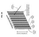
- FIG. 3Aillustrates an example of a fluorescent screen having color phosphor stripes that can be used in a post-objective scanning beam display system.
- FIG. 3Bshows an exemplary design of the screen in FIG. 3A .
- FIG. 3Cshows the operation of the screen in a view along the direction perpendicular to the surface of the screen in FIG. 3A .
- FIG. 4shows another exemplary design of the screen in
- FIG. 3Ais a diagrammatic representation of FIG. 3A .
- FIG. 5shows an example of a post-objective scanning beam display system based on the system design in FIG. 1 .
- FIGS. 6A , 6 B and 6 Cillustrate a specific example of the post-objective design of the beam scanning module in FIG. 5 .
- FIGS. 7 , 8 and 9show various image effects on the screen of a post-objective scanning system.
- FIG. 10shows an example of a post-objective scanning display based on a folded optical rear projection design.
- FIGS. 11-13show examples of the vertical scanner for post-objective scanning systems.
- Examples of post-objective scanning-beam systems described in this applicationuse a vertical scanner with an optical reflector and a spinning horizontal polygon scanner with reflective facets to provide the 2-dimensional scanning of one or more scanning beams onto a target screen.
- a beamcan be first directed to a first scanner of the vertical scanner and the polygon scanner to scan along a first direction and then directed through a scan lens located between the vertical scanner and the polygon scanner. After exiting the scan lens, the beam is scanned along the first direction and is directed to the second scanner of the vertical scanner and the polygon scanner to scan along a second, different direction (e.g., orthogonal to the first direction).
- the output of the second scanneris a scanning beam that is scanned along both the first and the second directions.
- FIG. 1shows an example implementation of a post-objective scanning system.
- a laser source 110is provided to produce at least one laser beam 112 .
- this single beamcan be a beam of a particular wavelength, e.g., a visible color, UV light or other wavelengths.
- multiple beams 112may be generated from the laser source 110 and are scanned.
- the different beams 112may be of different wavelengths, e.g., red, green and blue colors in the visible range, or of the same or similar wavelengths, e.g., UV light.
- the first scanner of the two scannersis a polygon scanner 140 .
- the beam 112is scanned along the first direction (e.g., the horizontal direction) by the polygon scanner 140 as a 1-D scanning beam 114 .
- the second scanner downstream from the polygon scanner 140is a vertical scanner 150 , e.g., a galvo mirror constructed by engaging a mirror to a galvanometer and operates to scan the horizontally scanning beam 114 along the vertical direction as a 2-D scanning beam 116 to a target surface 101 , e.g., a screen.
- a scan lens 120is placed between the two scanners 140 and 150 .
- the scan lens 120can be structured to have high optical performance in focusing the 1-D scanning beam 114 along the scanning direction of the first scanner 140 only. Hence, such a scan lens does need to exhibit high optical performance along the second scanning direction (i.e., the vertical direction in this example) because the beam 114 is not scanned along the second scanning direction at the position of the scan lens 120 . Therefore, the scan lens 120 can be a 1-D scan lens, e.g., a 1-D f theta lens. High-cost and complex 2-D lenses can be avoided in implementing the system of FIG. 1 . Due to the design of the scan lens 120 , the focusing of the beam 116 on the target surface 101 does not change with the horizontal scanning.
- the vertical scanner 150 in FIG. 1scans at a much smaller rate as the second scanner than the scan rate of the first horizontal scanner 140 and thus a focusing variation caused by the vertical scanning on the target surface 101 varies with time at the slower vertical scanning rate.
- this particular arrangement of two scanners 140 and 150allows easy implementation of the dynamic focusing adjustment to maintain the proper focusing of the 2-D scanning beam on the target surface as the vertical scanner 150 scans along the vertical direction.
- the target surface 101 in FIG. 1is a surface of a target device 102 .
- the device 102can be in various forms depending on the applications of the system in FIG. 1 .
- the target device 102can be a screen on which images carried by the scanning beam 116 are displayed in a way visible to a viewer.
- the beam 112 incident to the first scanner 140is optically modulated to carry the images to be displayed on the screen 102 .
- FIGS. 2A and 2Bshow two optical modulation designs that can be used to modulate the beam 112 to carry images or other information.
- a laser 210such as a diode laser is directly modulated to produce a modulated beam 112 that carries the image signals, e.g., color image data in red, green and blue.
- the laser source 110 in this implementationincludes a signal modulation controller 220 which modulates the laser 210 directly.
- the signal modulation controller 220can control the driving current of a laser diode as the laser 210 .
- a laser 230is used to generate a CW unmodulated laser beam 232 and an optical modulator 240 is used to modulate the CW laser beam 232 with the image signals in red, green and blue and to produce the modulated beam 112 .
- a signal modulation controller 250is used to control the optical modulator 240 .
- an acousto-optic modulator or an electro-optic modulatormay be used as the optical modulator 240 .
- the screen 102can be passive screens and active screens.
- a passive screendoes not emit light but makes light of the one or more scanning beams visible to a viewer by one or a combination of mechanisms, such as optical reflection, optical diffusion, optical scattering and optical diffraction.
- a passive screencan reflect or scatter received scanning beam(s) to show images.
- An active screenemits light by absorbing the one or more scanning beams and the emitted light forms part of or all of the light that forms the displayed images.
- Such an active screenmay include one or more fluorescent materials to emit light under optical excitation of the one or more scanning beams received by the screen to produce images.
- the term “a fluorescent material”is used here to cover both fluorescent materials and phosphorescent materials. Screens with phosphor materials under excitation of one or more scanning excitation laser beams are described here as specific implementation examples of optically excited fluorescent or phosphorescent materials in various systems.
- Various screen designs with fluorescent materialscan be used. Screens with phosphor materials under excitation of one or more scanning excitation laser beams are described in detail and are used as specific implementation examples of optically excited fluorescent materials in various system and device examples in this application.
- three different color phosphors that are optically excitable by the laser beam to respectively produce light in red, green, and blue colors suitable for forming color imagescan be formed on the screen as repetitive red, green and blue phosphor stripes in parallel.
- Various examples described in this applicationuse screens with parallel color phosphor stripes for emitting light in red, green, and blue to illustrate various features of the laser-based displays.
- Phosphor materialsare one type of fluorescent materials.
- Various described systems, devices and features in the examples that use phosphors as the fluorescent materialsare applicable to displays with screens made of other optically excitable, light-emitting, non-phosphor fluorescent materials.
- quantum dot materialsemit light under proper optical excitation and thus can be used as the fluorescent materials for systems and devices in this application.
- semiconductor compoundssuch as, among others, CdSe and PbS, can be fabricated in form of particles with a diameter on the order of the exciton Bohr radius of the compounds as quantum dot materials to emit light.
- different quantum dot materials with different energy band gap structuresmay be used to emit different colors under the same excitation light.
- Some quantum dotsare between 2 and 10 nanometers in size and include approximately tens of atoms such between 10 to 50 atoms. Quantum dots may be dispersed and mixed in various materials to form liquid solutions, powders, jelly-like matrix materials and solids (e.g., solid solutions).
- Quantum dot films or film stripesmay be formed on a substrate as a screen for a system or device in this application.
- three different quantum dot materialscan be designed and engineered to be optically excited by the scanning laser beam as the optical pump to produce light in red, green, and blue colors suitable for forming color images.
- Such quantum dotsmay be formed on the screen as pixel dots arranged in parallel lines (e.g., repetitive sequential red pixel dot line, green pixel dot line and blue pixel dot line).
- Some implementations of post-objective scanning beam display systems described hereuse at least one scanning laser beam to excite color light-emitting materials deposited on a screen to produce color images.
- the scanning laser beamis modulated to carry images in red, green and blue colors or in other visible colors and is controlled in such a way that the laser beam excites the color light-emitting materials in red, green and blue colors with images in red, green and blue colors, respectively.
- the scanning laser beamcarries the images but does not directly produce the visible light seen by a viewer. Instead, the color light-emitting fluorescent materials on the screen absorb the energy of the scanning laser beam and emit visible light in red, green and blue or other colors to generate actual color images seen by the viewer.
- Laser excitation of the fluorescent materials using one or more laser beams with energy sufficient to cause the fluorescent materials to emit light or to luminesceis one of various forms of optical excitation.
- the optical excitationmay be generated by a non-laser light source that is sufficiently energetic to excite the fluorescent materials used in the screen.
- non-laser excitation light sourcesinclude various light-emitting diodes (LEDs), light lamps and other light sources that produce light at a wavelength or a spectral band to excite a fluorescent material that converts the light of a higher energy into light of lower energy in the visible range.
- the excitation optical beam that excites a fluorescent material on the screencan be at a frequency or in a spectral range that is higher in frequency than the frequency of the emitted visible light by the fluorescent material. Accordingly, the excitation optical beam may be in the violet spectral range and the ultra violet (UV) spectral range, e.g., wavelengths under 420 nm.
- UV light or a UV laser beamis used as an example of the excitation light for a phosphor material or other fluorescent material and may be light at other wavelength.
- FIG. 3Aillustrates an example of a fluorescent screen 301 having color phosphor stripes.
- color phosphor dotsmay also be used to define the image pixels on the screen.
- the screen 301has parallel color phosphor stripes in the vertical direction where red phosphor absorbs the laser light to emit light in red, green phosphor absorbs the laser light to emit light in green and blue phosphor absorbs the laser light to emit light in blue. Adjacent three color phosphor stripes are in three different colors. One particular spatial color sequence of the stripes is shown in FIG. 3A as red, green and blue. Other color sequences may also be used.
- the laser beam 116is at the wavelength within the optical absorption bandwidth of the color phosphors and is usually at a wavelength shorter than the visible blue and the green and red colors for the color images.
- the color phosphorsmay be phosphors that absorb UV light in the spectral range from about 380 nm to about 420 nm to produce desired red, green and blue light.
- FIG. 3Bshows an exemplary design of the screen 301 in FIG. 3A .
- the screen 301 in this particular exampleincludes a rear substrate 311 which is transparent to the scanning laser beam 116 to receive the scanning laser beam 116 .
- a second front substrate 312is fixed relative to the rear substrate 311 and faces the viewer so that the fluorescent light transmits through the substrate 312 towards the viewer.
- a color phosphor stripe layer 310is placed between the substrates 311 and 312 and includes phosphor stripes.
- the color phosphor stripes for emitting red, green and blue colorsare represented by “R”, “G” and “B,” respectively.
- the front substrate 312is transparent to the red, green and blue colors emitted by the phosphor stripes.
- the substrates 311 and 312may be made of various materials, including glass or plastic panels.
- Each color pixelincludes portions of three adjacent color phosphor stripes in the horizontal direction and its vertical dimension is defined by the beam spread of the laser beam 116 in the vertical direction. As such, each color pixel includes three subpixels of three different colors (e.g., the red, green and blue).
- the scanning laser beam 116is directed at the green phosphor stripe within a pixel to produce green light for that pixel.
- FIG. 3Cfurther shows the operation of the screen 301 in a view along the direction perpendicular to the surface of the screen 301 .
- the cross section of the beam 116may be shaped to be elongated along the direction of the stripe to maximize the fill factor of the beam within each color stripe for a pixel. This may be achieved by using a beam shaping optical element.
- a laser source that is used to produce a scanning laser beam that excites a phosphor material on the screenmay be a single mode laser or a multimode laser. The laser may also be a single mode along the direction perpendicular to the elongated direction phosphor stripes to have a small beam spread that is confined by the width of each phosphor stripe.
- this laser beammay have multiple modes to spread over a larger area than the beam spread in the direction across the phosphor stripe.
- This use of a laser beam with a single mode in one direction to have a small beam footprint on the screen and multiple modes in the perpendicular direction to have a larger footprint on the screenallows the beam to be shaped to fit the elongated color subpixel on the screen and to provide sufficient laser power in the beam via the multimodes to ensure sufficient brightness of the screen.
- FIG. 4illustrates an example of a fluorescent screen design that has a contiguous and uniform layer 420 of mixed phosphors.
- This mixed phosphor layer 420is designed and constructed to emit white light under optical excitation of the excitation light 116 .
- the mixed phosphors in the mixed phosphor layer 420can be designed in various ways and a number of compositions for the mixed phosphors that emit white light are known and documented.
- a layer 410 of color filters, such as stripes of red-transmitting, green-transmitting and blue-transmitting filters,is placed on the viewer side of the mixed phosphor layer 420 to filter the white light and to produce colored output light.
- the layers 410 and 420can be sandwiched between substrates 401 and 402 .
- the color filtersmay be implemented in various configurations, including in designs similar to the color filters used in color LCD panels.
- each color filter regione.g., a red-transmitting filter
- the filtertransmits the red light and absorbs light of other colors including green light and blue light.
- Each filter in the layer 410may be a multi-layer structure that effectuates a band-pass interference filter with a desired transmission band.
- Various designs and techniquesmay be used for designing and constructing such filters.
- a fluorescent stripe in the fluorescent screen in various examples described in this applicationis a fluorescent stripe that emits a designated color under optical excitation and can be either a fluorescent stripe formed of a particular fluorescent material that emits the designated color in FIG. 3A or a combination of a stripe color filter and a white fluorescent layer in FIG. 4 .
- FIG. 5shows an example implementation of a post-objective scanning beam display system based on the system design in FIG. 1 .
- a laser array 510 with multiple lasersis used to generate multiple laser beams 512 to simultaneously scan a screen 501 for enhanced display brightness.
- the screen 501can be a passive screen or an active screen.
- the laser array 510can be implemented in various configurations, such as discrete laser diodes on separate chips arranged in an array and a monolithic laser array chip having integrated laser diodes arranged in an array.
- a signal modulation controller 520is provided to control and modulate the lasers in the laser array 510 so that the laser beams 512 are modulated to carry the image to be displayed on the screen 501 .
- the signal modulation controller 520can include a digital image processor which generates the digital image signals for the three different color channels and laser driver circuits that produce laser control signals carrying the digital image signals.
- the laser control signalsare then applied to modulate the lasers in the laser array 510 , e.g., electric currents that drive the laser diodes.
- the laser beams 512can be of different wavelengths (e.g., red, green and blue colors for a display with a passive screen 501 ) or of the same wavelength (e.g., either to increase the intensity of light to produce a monochromatic pattern on a passive surface 501 or an excitation light beam that excites phosphors on an active phosphor screen 501 in FIG. 3A ).
- the beam scanningis based on a two-scanner system in FIG. 1 .
- Each of the different reflective facets of the polygon scanner 140simultaneously scans N horizontal lines where N is the number of lasers.
- a relay optics module 530reduces the spacing of laser beams 512 to form a compact set of laser beams 532 that spread within the facet dimension of the polygon scanner 140 for the horizontal scanning.
- a 1-D horizontal scan lens 120Downstream from the polygon scanner 140 , there is a 1-D horizontal scan lens 120 followed by a vertical scanner 150 (e.g., a galvo mirror) that receives each horizontally scanned beam 532 from the polygon scanner 140 through the 1-D scan lens 120 and provides the vertical scan on each horizontally scanned beam 532 at the end of each horizontal scan prior to the next horizontal scan by the next facet of the polygon scanner 140 .
- a vertical scanner 150e.g., a galvo mirror
- the 1-D scan lens 120is placed downstream from the polygon scanner 140 and upstream from the vertical scanner 150 to focus each horizontal scanned beam on the screen 501 and minimizes the horizontal bow distortion to displayed images on the screen 501 within an acceptable range, thus producing a visually “straight” horizontal scan line on the screen 501 .
- Such a 1-D scan lens 120 capable of producing a straight horizontal scan lineis relatively simpler and less expensive than a 2-D scan lens of similar performance.
- the vertical scanner 150Downstream from the scan lens 120 , the vertical scanner 150 is a flat reflector and simply reflects the beam to the screen 501 and scans vertically to place each horizontally scanned beam at different vertical positions on the screen 501 for scanning different horizontal lines.
- the dimension of the reflector on the vertical scanner 150 along the horizontal directionis sufficiently large to cover the spatial extent of each scanning beam coming from the polygon scanner 140 and the scan lens 120 .
- the system in FIG. 5is a post-objective design because the 1-D scan lens 120 is upstream from the vertical scanner 150 . In this particular example, there is no lens or other focusing element downstream from the vertical scanner 150 .
- This optical designeliminates the need for a complex and expensive 2-D scan lens 120 in pre-objective scanning beam displays where the scanning lens is located downstream from the two scanners 140 and 150 and focuses the a scanning excitation beam onto a screen.
- a scanning beam directed into the scan lensis scanned along two orthogonal directions. Therefore, the scan lens is designed to focus the scanning beam onto the screen along two orthogonal directions.
- the scan lenscan be complex and, often, are made of multiples lens elements.
- the scan lenscan be a two-dimensional f-theta lens that is designed to have a linear relation between the location of the focal spot on the screen and the input scan angle (theta) when the input beam is scanned around each of two orthogonal axes perpendicular to the optic axis of the scan lens.
- the location of the focal spot on the screenis a proportional to the input scan angle (theta).
- the two-dimensional scan lenssuch as a f-theta lens in the pre-objective configuration can exhibit optical distortions along the two orthogonal scanning directions which cause beam positions on the screen to trace a curved line. Hence, an intended straight horizontal scanning line on the screen becomes a curved line.
- the distortions caused by the 2-dimensional scan lenscan be visible on the screen and thus degrade the displayed image quality.
- One way to mitigate the bow distortion problemis to design the scan lens with a complex lens configuration with multiple lens elements to reduce the bow distortions.
- the complex multiple lens elementscan cause the final lens assembly to depart from desired f-theta conditions and thus can compromise the optical scanning performance.
- the number of lens elements in the assemblyusually increases as the tolerance for the distortions decreases.
- such a scan lens with complex multiple lens elementscan be expensive to fabricate.
- the following sectionsdescribe examples of a post-objective scanning beam display system, which can be implemented to replace the two-dimensional scan lens with a simpler, less expensive 1-dimensional scan lens 120 shown in FIG. 5 .
- FIGS. 6A , 6 B and 6 Cillustrate a specific example of the post-objective design of the beam scanning module in FIG. 5 .
- the 1-D scan lens 120can be a compound lens with multiple lens elements to achieve desired 1-D focusing of a horizontally scanned beam with no horizontal bow distortion.
- the 1-D scan lens 120can have an elongated shape along the horizontal scanning direction of the beam and is placed within the same plane 600 that is perpendicular to the vertical polygon rotation axis.
- the vertical scanner 150pivots around a horizontal axis which lies in the plane 600 . The pivoting of the vertical scanner 150 directs beams reflected from different polygon facets to different vertical directions to trace out different horizontal scan lines on the screen 501 .
- FIG. 6Bshows the cross section view of the beam scanning module 4920 along the lines BB in FIG. 6A which is a view along the lines AA in FIG. 6B .
- FIG. 6Cfurther shows a perspective view of the beam scanning module 4920 to show different horizontal positions of a horizontally scanned beam by along a straight horizontal line from a single polygon facet.
- the 1-D scan lens 120 in the above exampleis a 4-element compound lens as shown in FIGS. 6A and 6B .
- the distance from the scan lens to a location on the screen 501 for a particular beamvaries with the vertical scanning position of the vertical scanner 150 . Therefore, when the 1-D scan lens 120 is designed to have a fixed focal distance along the straight horizontal line across the center of the elongated 1-D scan lens, the focal properties of each beam must change with the vertical scanning position of the vertical scanner 150 .
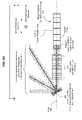
- FIG. 7illustrates examples of the changes in the beam size and shape on the screen 501 for the post-objective design in FIGS. 6A-6C along different horizontal positions on the screen 501 .
- this spot diagram for a horizontal set of beams at different horizontal positions and the same vertical position on the screenthe end spots located on two sides of the screen are more elongated because of the large angle of incidence of the laser which is about 42 degrees in the setup for the measurements shown.
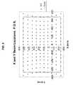
- FIG. 8further shows beam widths at different representative positions on the screen 501 : middle center, middle edge, top center and top corner or edge.
- a dynamic focusing mechanismis implemented to adjust convergence of the beam going into the 1-D scan lens 120 based on the vertical scanning position of the vertical scanner 150 .
- a stationary lens 620 and a dynamic refocus lens 630are used as the dynamic focusing mechanism.
- Each beamis focused by the dynamic focus lens 630 at a location upstream from the stationary lens 620 .
- the output light from the lens 620is collimated.
- the output light from the collimator lens 620 toward the polygon scanner 140can be either divergent or convergent.
- the lens 620may be adjustable while the lens 630 is fixed in position or both lenses 620 and 630 are adjustable to change their positions for changing the focus of the beam sent to the screen.
- a refocusing lens actuator 640can be used to adjust the relative position between the lenses 620 and 630 in response to a control signal 650 .
- the refocusing lens actuator 5410is used to adjust the convergence of the beam directed into the 1-D scan lens 120 along the optical path from the polygon scanner 140 in synchronization with the vertical scanning of the vertical scanner 150 .
- the actuator 640is controlled to adjust the position of the lens 630 relative to an upstream focal point of the lens 620 to change the beam convergence at the entry of the 1-D scan lens 120 .
- a control modulecan be provided to synchronize the actuator 640 and the vertical scanner 150 by sending a refocusing control signal 650 to control the operation of actuator 640 .
- the adjustmentcan be a distance of less than 10 microns at the lens 630 to provide sufficient refocusing for a screen of over 60′′ in the diagonal dimension.
- the change of the distance from the scan lens 120 to a location on the screen 501 for a particular beam due to different vertical scanning positions of the vertical scanner 150also creates a vertical bow distortion on the screen 501 .
- the vertical scanner 150directs a beam to the center of the screen 501 when the vertical angle of the vertical scanner 150 is at zero where the distance between the screen 501 and the vertical scanner 150 is the shortest.
- the vertical scanner 150changes its vertical orientation in either vertical scanning direction, the horizontal dimension of each horizontal line increases with the vertical scanning angle.
- FIG. 9illustrates this bow distortion. Different from classical barrel distortions in lenses, this distortion is geometrical in nature and is caused by the change in the vertical scanning angle of the vertical scanner 150 . This distortion essentially changes the beam spot spacing of beam spots from a regular chain of optical pulses in each scanning beam along the horizontal direction across the screen 501 . Therefore, controlling timing of laser pulses in the scanning beam during each horizontal scan can be applied to correct this distortion.
- the time delay in timing of a pulsecan cause the corresponding position of the laser pulse on the screen to spatially shift downstream along the horizontal scan direction.
- an advance in timing of a pulsecan cause the corresponding position of the laser pulse on the screen to spatially shift upstream along the horizontal scan direction.
- a position of a laser pulse on the screen in the horizontal directioncan be controlled electronically or digitally by controlling timing of optical pulses in the scanning beam. Therefore, the timing of the pulses in the scanning beam can be controlled to direct each optical pulse to a location that reduces or offsets the horizontal displacement of the beam caused by the vertical scanning of the vertical scanner 150 .
- the timing of the laser pulsesis then controlled during each horizontal scanning to offset the obtained amounts of the horizontal position shift at different beam locations and at different vertical scanner positions.
- this control of the timing of laser pulsesis separate from, and can be simultaneously implemented with, the control of timing of laser pulses in aligning laser pulses to proper phosphor color stripes during a horizontal scan based on the servo feedback described in PCT patent application No. PCT/US2007/004004 entitled “Servo-Assisted Scanning Beam Display Systems Using Fluorescent Screens” and filed Feb. 15, 2007 and published as PCT publication No.
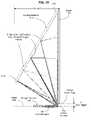
- FIG. 10shows one example of a rear-projection display based on a post-objective scanning beam design of this application.
- the screen 501is placed above the plane 500 in which the polygon scanner 140 , the 1-D scan lens 120 and the center of the vertical scanner 150 are located.
- the screen lower edge of the display area (e.g., the area with fluorescent stripes in FIG. 3A ) of the screen 501is above the plane 600 by a chin height H. It can be desirable to reduce the chin height H in such systems to reduce the size of the display. It can also be desirable to reduce the depth D of the display to about 13.5′′ or less.
- a combination of the folded optical path and the post-objective configurationallows both H and D to be minimized.
- the screen 501can be approximately perpendicular to the plane 600 .
- a folding reflector 1010is provided at the excitation side of the screen 501 to reflect light from the vertical scanner 150 to the screen 501 .
- the reflector 1010can be oriented at an angle with respect to the screen 501 and has one end 1011 to be close to or in contact with the upper side of the active display area of the screen 501 to reflect light to the upper side the active display area.
- the dimension and angle of the reflector 1010are set to allow the other end 1012 of the reflector 1010 to reflect light from the vertical scanner 150 near the lower edge of the active area of the screen 501 .
- the vertical scanner 150can be placed as close to the inner side of the screen 501 as possible to minimize the depth D of the display.
- the 1-D scan lensis placed downstream from the polygon horizontal scanner 140 which provides a high-speed horizontal scan (e.g., 1080 successive scans per frame for a 1080-p display) and upstream from the vertical scanner 150 which provides a lower speed vertical scan (e.g., one scan per frame).
- the refocusing control by the actuator 640is synchronized with the lower-speed vertical scan of the vertical scanner 150 and thus allows for a slower actuator to be used as the actuator 640 for the refocusing. Accordingly, various issues associated with using a high-speed actuator for the refocusing mechanism, such as cost, feasibility, and refocusing speed and accuracy are avoided.
- the vertical scanner 150has a dimension W sufficiently large to receive the horizontally scanned beam from the 1-D scan lens 120 .
- This dimension Wis much larger (e.g., 134 mm) than the vertical scanner used in pre-objective scanning system and can present technical issues in designing the vertical scanner 150 .
- the distortion in the shape of the vertical scanner 150can distort a horizontal scan line and thus compromise the image quality.
- Electromagnetic galvo mirrorscan be used to implement the vertical scanner 150 .
- FIGS. 11 , 12 and 13illustrate three examples where the coils are designed to provide a torque along the full length of the mirror.
- FIG. 11shows a permanent magnet type rotor with a slotted stator.
- FIG. 12a permanent magnet type rotor with smooth stator windings is shown.
- FIG. 13shows a stepper motor type galvo motor-mirror where the mirror can be hollowed out to reduce the inertia.
- the various servo control techniques described in connection with the pre-objective display systemscan be applied to the post-objective scanning beam displays.
- the post-objective scanning beam systems based on the designs described in this applicationcan be applied to display systems and other optical systems that use scanning beams to produce optical patterns.
- laser printing systemscan also use the above described post-objective scanning systems where the screen is replaced by a printing medium (e.g., paper, fabric, or a master printing plate).
Landscapes
- Physics & Mathematics (AREA)
- Optics & Photonics (AREA)
- General Physics & Mathematics (AREA)
- Engineering & Computer Science (AREA)
- Multimedia (AREA)
- Signal Processing (AREA)
- Mechanical Optical Scanning Systems (AREA)
Abstract
Description
Claims (23)
Priority Applications (3)
| Application Number | Priority Date | Filing Date | Title |
|---|---|---|---|
| US11/742,014US7697183B2 (en) | 2007-04-06 | 2007-04-30 | Post-objective scanning beam systems |
| US12/594,938US8045247B2 (en) | 2007-04-06 | 2008-04-07 | Post-objective scanning beam systems |
| PCT/US2008/059603WO2008124707A1 (en) | 2007-04-06 | 2008-04-07 | Post-objective scanning beam systems |
Applications Claiming Priority (2)
| Application Number | Priority Date | Filing Date | Title |
|---|---|---|---|
| US91064407P | 2007-04-06 | 2007-04-06 | |
| US11/742,014US7697183B2 (en) | 2007-04-06 | 2007-04-30 | Post-objective scanning beam systems |
Related Child Applications (1)
| Application Number | Title | Priority Date | Filing Date |
|---|---|---|---|
| US12/594,938ContinuationUS8045247B2 (en) | 2007-04-06 | 2008-04-07 | Post-objective scanning beam systems |
Publications (2)
| Publication Number | Publication Date |
|---|---|
| US20080247020A1 US20080247020A1 (en) | 2008-10-09 |
| US7697183B2true US7697183B2 (en) | 2010-04-13 |
Family
ID=39826640
Family Applications (2)
| Application Number | Title | Priority Date | Filing Date |
|---|---|---|---|
| US11/742,014Active2028-06-20US7697183B2 (en) | 2007-04-06 | 2007-04-30 | Post-objective scanning beam systems |
| US12/594,938ActiveUS8045247B2 (en) | 2007-04-06 | 2008-04-07 | Post-objective scanning beam systems |
Family Applications After (1)
| Application Number | Title | Priority Date | Filing Date |
|---|---|---|---|
| US12/594,938ActiveUS8045247B2 (en) | 2007-04-06 | 2008-04-07 | Post-objective scanning beam systems |
Country Status (2)
| Country | Link |
|---|---|
| US (2) | US7697183B2 (en) |
| WO (1) | WO2008124707A1 (en) |
Cited By (12)
| Publication number | Priority date | Publication date | Assignee | Title |
|---|---|---|---|---|
| US20070188417A1 (en)* | 2006-02-15 | 2007-08-16 | Hajjar Roger A | Servo-assisted scanning beam display systems using fluorescent screens |
| US20080284988A1 (en)* | 2007-05-18 | 2008-11-20 | Sony Corporation | Image projecting apparatus and image projecting method for use in the same |
| US20080316373A1 (en)* | 2007-04-24 | 2008-12-25 | Sanyo Electric Co., Ltd. | Projection type image display device |
| US20090116107A1 (en)* | 2007-05-17 | 2009-05-07 | David Kindler | Multilayered Screens with Light-Emitting Stripes for Scanning Beam Display Systems |
| US20090174632A1 (en)* | 2005-04-01 | 2009-07-09 | Hajjar Roger A | Laser Displays Using Phosphor Screens Emitting Visible Colored Light |
| US20100097678A1 (en)* | 2007-06-27 | 2010-04-22 | Spudnik, Inc. | Servo Feedback Control Based on Designated Scanning Servo Beam in Scanning Beam Display Systems with Light-Emitting Screens |
| US20110068466A1 (en)* | 2009-09-22 | 2011-03-24 | Taiwan Semiconductor Manufacturing Company, Ltd. | Wafer Backside Interconnect Structure Connected to TSVs |
| US20110176208A1 (en)* | 2006-03-31 | 2011-07-21 | Prysm, Inc. | Multilayered Fluorescent Screens for Scanning Beam Display Systems |
| US8089425B2 (en) | 2006-03-03 | 2012-01-03 | Prysm, Inc. | Optical designs for scanning beam display systems using fluorescent screens |
| DE102012019392A1 (en) | 2011-10-04 | 2013-06-13 | Prysm, Inc. | COMPOSITE AND OTHER FLUORESCENT MATERIALS FOR THE DISTRIBUTION OF VISIBLE LIGHT AND APPLICATIONS FOR THE PRODUCTION OF VISIBLE LIGHT COMPRISING LIGHT-EMITTING UMBRELLAS |
| US8698713B2 (en) | 2005-04-01 | 2014-04-15 | Prysm, Inc. | Display systems having screens with optical fluorescent materials |
| US9261723B1 (en) | 2008-02-01 | 2016-02-16 | Prysm, Inc. | Reducing visibility of inter-screen gap in tiled display systems |
Families Citing this family (16)
| Publication number | Priority date | Publication date | Assignee | Title |
|---|---|---|---|---|
| US7733310B2 (en) | 2005-04-01 | 2010-06-08 | Prysm, Inc. | Display screens having optical fluorescent materials |
| US7994702B2 (en) | 2005-04-27 | 2011-08-09 | Prysm, Inc. | Scanning beams displays based on light-emitting screens having phosphors |
| US7884816B2 (en) | 2006-02-15 | 2011-02-08 | Prysm, Inc. | Correcting pyramidal error of polygon scanner in scanning beam display systems |
| US8013506B2 (en) | 2006-12-12 | 2011-09-06 | Prysm, Inc. | Organic compounds for adjusting phosphor chromaticity |
| GB2460802B (en) | 2007-03-20 | 2012-09-05 | Prysm Inc | Delivering and displaying advertisment or other application data to display systems |
| US8169454B1 (en) | 2007-04-06 | 2012-05-01 | Prysm, Inc. | Patterning a surface using pre-objective and post-objective raster scanning systems |
| CN101690244A (en)* | 2007-06-27 | 2010-03-31 | 皇家飞利浦电子股份有限公司 | Laser scanning projection equipment |
| US7878657B2 (en) | 2007-06-27 | 2011-02-01 | Prysm, Inc. | Servo feedback control based on invisible scanning servo beam in scanning beam display systems with light-emitting screens |
| CA2703345C (en) | 2007-10-22 | 2016-04-12 | Endocross Ltd. | Balloons and balloon catheter systems for treating vascular occlusions |
| US7869112B2 (en)* | 2008-07-25 | 2011-01-11 | Prysm, Inc. | Beam scanning based on two-dimensional polygon scanner for display and other applications |
| US20110305000A1 (en)* | 2010-06-09 | 2011-12-15 | Bukesov Sergey A | Display screen with low-index region surrounding phospors |
| USD711883S1 (en)* | 2013-03-15 | 2014-08-26 | Meditory Llc | Scanner |
| US10459114B2 (en)* | 2015-05-18 | 2019-10-29 | Lasermotive, Inc. | Wireless power transmitter and receiver |
| USD757010S1 (en)* | 2015-05-28 | 2016-05-24 | Hewlett-Packard Development Company, L.P. | Scanner turntable |
| US10694158B2 (en)* | 2017-06-28 | 2020-06-23 | Canyon Product Development, LLC | Image projector |
| CN113199160B (en)* | 2021-05-08 | 2022-06-17 | 济南森峰激光科技股份有限公司 | Laser synchronous scanning group hole machining system and scanning method |
Citations (192)
| Publication number | Priority date | Publication date | Assignee | Title |
|---|---|---|---|---|
| US2439181A (en) | 1946-05-17 | 1948-04-06 | Rca Corp | Luminescent screen |
| US3025161A (en) | 1955-06-27 | 1962-03-13 | Sylvania Electric Prod | Method of forming patterns |
| US3556637A (en) | 1968-06-27 | 1971-01-19 | Minnesota Mining & Mfg | Reflex-reflecting aggregate and markers prepared therefrom |
| US3652956A (en) | 1970-01-23 | 1972-03-28 | Bell Telephone Labor Inc | Color visual display |
| US3691482A (en) | 1970-01-19 | 1972-09-12 | Bell Telephone Labor Inc | Display system |
| US3750189A (en) | 1971-10-18 | 1973-07-31 | Ibm | Light scanning and printing system |
| US4165154A (en) | 1976-10-05 | 1979-08-21 | Sanyo Electric Co., Ltd. | Projection screen assembly |
| US4166233A (en) | 1977-06-13 | 1979-08-28 | Rca Corporation | Phosphor screen for flat panel color display |
| US4307320A (en) | 1978-02-03 | 1981-12-22 | Kasei Optonix, Ltd. | Pigment coated phosphor and high contrast color television cathode ray tube using same |
| US4401362A (en) | 1980-07-15 | 1983-08-30 | Olympus Optical Co., Ltd. | f-θ Lens system |
| US4512911A (en) | 1979-06-19 | 1985-04-23 | Kasei Optonix, Ltd. | Phosphor |
| US4613201A (en) | 1982-01-19 | 1986-09-23 | Dwight Cavendish Co., Ltd. | Light projection apparatus |
| US4624528A (en) | 1985-02-21 | 1986-11-25 | Xerox Corporation | Scanning systems with polygon scanner having curved facets |
| US4661419A (en) | 1984-07-31 | 1987-04-28 | Fuji Photo Film Co., Ltd. | Phosphor and radiation image storage panel containing the same |
| US4707093A (en) | 1985-06-04 | 1987-11-17 | Videocolor | Method and device for illuminating the face plate of a color television tube for formation of the screen |
| US4737840A (en) | 1983-07-31 | 1988-04-12 | Nec Home Electronics Ltd. | Color image projection apparatus with a screen including a shield plate, light-emitting layer and diffusion surface to expand viewing range of bright pictures |
| US4816920A (en) | 1986-11-18 | 1989-03-28 | General Scanning, Inc. | Planar surface scanning system |
| US4923262A (en) | 1985-11-06 | 1990-05-08 | Holographix, Inc. | Scanner system having rotating deflector hologram |
| US4978202A (en) | 1989-05-12 | 1990-12-18 | Goldstar Co., Ltd. | Laser scanning system for displaying a three-dimensional color image |
| US4979030A (en) | 1988-11-30 | 1990-12-18 | Pioneer Electronic Corporation | Color display apparatus |
| EP0271650B1 (en) | 1986-10-10 | 1991-04-10 | Seton Health Care Foundation | Three-dimensional laser driven display apparatus |
| EP0196862B1 (en) | 1985-03-26 | 1991-09-11 | Sony Corporation | Cathode ray tubes |
| US5054866A (en)* | 1988-12-29 | 1991-10-08 | Ricoh Company, Ltd. | Scanning optical apparatus |
| US5080467A (en) | 1989-03-03 | 1992-01-14 | Greyhawk Systems, Inc | Biphenyl derivatives for photostabilization in pulsed optical darkening apparatus and method |
| US5089907A (en) | 1990-01-17 | 1992-02-18 | Matsushita Electric Industrial Co., Ltd. | Post-objective type optical scanner and image forming apparatus using the same |
| US5094788A (en) | 1990-12-21 | 1992-03-10 | The Dow Chemical Company | Interfacial surface generator |
| US5122905A (en) | 1989-06-20 | 1992-06-16 | The Dow Chemical Company | Relective polymeric body |
| US5136426A (en) | 1991-02-27 | 1992-08-04 | Advanced Laser Projection, Inc. | Light projection apparatus |
| US5138441A (en) | 1989-07-07 | 1992-08-11 | Pioneer Electronic Corporation | Beam-index-type color display apparatus |
| US5140604A (en) | 1990-03-13 | 1992-08-18 | Quartz Et Silice | Mixed strontium and lanthanide oxides and a laser using monocrystals of these oxides |
| US5146355A (en) | 1986-10-23 | 1992-09-08 | Litton Systems Canada Limited | Transflective mode liquid crystal display with phosphor illumination |
| US5166944A (en) | 1991-06-07 | 1992-11-24 | Advanced Laser Technologies, Inc. | Laser beam scanning apparatus and method |
| US5175637A (en) | 1990-04-05 | 1992-12-29 | Raychem Corporation | Displays having improved contrast |
| US5182659A (en) | 1991-02-20 | 1993-01-26 | Holographix, Inc. | Holographic recording and scanning system and method |
| US5198679A (en) | 1984-11-16 | 1993-03-30 | Fuji Photo Film Co., Ltd. | Phosphor and image storage panel |
| US5255113A (en) | 1991-04-03 | 1993-10-19 | Matsushita Electric Industrial Co., Ltd. | Pos-objective type optical scanner |
| US5269995A (en) | 1992-10-02 | 1993-12-14 | The Dow Chemical Company | Coextrusion of multilayer articles using protective boundary layers and apparatus therefor |
| US5270842A (en) | 1991-02-20 | 1993-12-14 | Holographix, Inc. | Holographic recording and scanning system and method |
| US5296922A (en) | 1991-04-04 | 1994-03-22 | Matsushita Electric Industrial Co., Ltd. | Projection television with a wavelength-selection-type rear projection screen |
| US5365288A (en) | 1992-10-01 | 1994-11-15 | Advanced Laser Projection, Inc. | Image mover |
| US5389324A (en) | 1993-06-07 | 1995-02-14 | The Dow Chemical Company | Layer thickness gradient control in multilayer polymeric bodies |
| US5414521A (en) | 1991-09-12 | 1995-05-09 | Ansley; David A. | Dynamic distortion correction apparatus and method |
| US5442254A (en) | 1993-05-04 | 1995-08-15 | Motorola, Inc. | Fluorescent device with quantum contained particle screen |
| US5473396A (en) | 1993-09-08 | 1995-12-05 | Matsushita Electric Industrial Co., Ltd. | Display apparatus and method of making the same |
| US5475524A (en) | 1994-12-19 | 1995-12-12 | Xerox Corporation | Optics for passive facet tracking and passive scan angle doubling |
| US5477285A (en) | 1993-10-06 | 1995-12-19 | Thomson Consumer Electronics, Inc. | CRT developing apparatus |
| US5477330A (en) | 1992-10-16 | 1995-12-19 | Printware, Inc. | Synchronization to a start-of-scan detection, and digital generation of variable frequencies, from a fixed-frequency fixed-phase frequency source in an image generator in order to highly accurately time the placement of pixels upon a scan line |
| US5491578A (en) | 1994-12-19 | 1996-02-13 | Xerox Corporation | Optics for passive scan angle doubling |
| US5526166A (en) | 1994-12-19 | 1996-06-11 | Xerox Corporation | Optical system for the correction of differential scanline bow |
| US5541731A (en) | 1995-04-28 | 1996-07-30 | International Business Machines Corporation | Interferometric measurement and alignment technique for laser scanners |
| US5550667A (en) | 1992-08-22 | 1996-08-27 | Alcatel N.V. | Optical transmitter |
| US5587818A (en) | 1994-12-26 | 1996-12-24 | Samsung Display Devices Co., Ltd. | Three color LCD with a black matrix and red and/or blue filters on one substrate and with green filters and red and/or blue filters on the opposite substrate |
| US5594556A (en) | 1993-03-28 | 1997-01-14 | Scitex Corporation Ltd. | Scanner having a misalignment detector |
| US5598292A (en) | 1992-03-02 | 1997-01-28 | Matsushita Electric Industrial Co., Ltd. | Method of designing a post-objective type optical scanner and product made by the method |
| US5602445A (en) | 1995-05-12 | 1997-02-11 | Oregon Graduate Institute Of Science And Technology | Blue-violet phosphor for use in electroluminescent flat panel displays |
| US5614961A (en) | 1993-02-03 | 1997-03-25 | Nitor | Methods and apparatus for image projection |
| US5633736A (en) | 1995-03-28 | 1997-05-27 | Eastman Kodak Company | Scan lens and an optical scanner system incorporating two deflectors |
| US5648181A (en) | 1992-09-14 | 1997-07-15 | Fuji Xerox Co., Ltd. | Inorganic thin film electroluminescent device having a light emission layer |
| US5666174A (en) | 1995-08-11 | 1997-09-09 | Cupolo, Iii; Anthony M. | Emissive liquid crystal display with liquid crystal between radiation source and phosphor layer |
| US5668662A (en) | 1994-05-12 | 1997-09-16 | Philips Electronics North America Corporation | Front projection screen with lenticular front surface |
| US5670209A (en) | 1995-04-24 | 1997-09-23 | Brite-Line Technologies, Inc. | High brightness durable retro-reflecting microspheres and method of making the same |
| US5684552A (en) | 1993-12-24 | 1997-11-04 | Sharp Kabushiki Kaisha | Color liquid crystal display having a color filter composed of multilayer thin films |
| US5698857A (en) | 1995-12-19 | 1997-12-16 | Eastman Kodak Company | (Barium hafnate: Cu) phosphors and phosphor screens |
| US5716118A (en) | 1995-10-25 | 1998-02-10 | Minolta Co., Ltd. | Imaging optical system |
| US5870224A (en) | 1995-10-25 | 1999-02-09 | Toppan Printing Company Limited | Lenticular sheet, rear-projection screen or TV using the same, and fabrication method for said lenticular sheet |
| US5882774A (en) | 1993-12-21 | 1999-03-16 | Minnesota Mining And Manufacturing Company | Optical film |
| US5907312A (en) | 1995-08-11 | 1999-05-25 | Sharp Kabushiki Kaisha | Three-dimensional image display device |
| US5959296A (en) | 1996-06-24 | 1999-09-28 | Eastman Chemical Company | Scanners for reading near infrared fluorescent marks |
| US5973813A (en) | 1997-06-13 | 1999-10-26 | Asahi Kogaku Kogyo Kabushiki Kaisha | Reflection type optical scanning system |
| US5978142A (en) | 1996-09-11 | 1999-11-02 | Seos Display, Limited | Image display apparatus with modulators for modulating picture elements in an image |
| US5976424A (en) | 1996-07-31 | 1999-11-02 | Minnesota Mining And Manufacturing Company | Method for making multilayer optical films having thin optical layers |
| US5994722A (en) | 1996-10-31 | 1999-11-30 | Siemens Aktiengesellschaft | Image display device that emits multicolored light |
| US5998925A (en) | 1996-07-29 | 1999-12-07 | Nichia Kagaku Kogyo Kabushiki Kaisha | Light emitting device having a nitride compound semiconductor and a phosphor containing a garnet fluorescent material |
| US5998918A (en) | 1996-12-13 | 1999-12-07 | Samsung Display Devices Co., Ltd. | Phosphor screen for a flickerless cathode ray tube and a process for preparing the same |
| US6008925A (en) | 1991-06-07 | 1999-12-28 | Advanced Laser Technologies, Inc. | Light beam scanning apparatus and method |
| US6010751A (en) | 1995-03-20 | 2000-01-04 | Delta V Technologies, Inc. | Method for forming a multicolor interference coating |
| US6057953A (en) | 1998-12-21 | 2000-05-02 | Xerox Corporation | Dual beam double pass raster output scanner |
| US6064417A (en) | 1998-03-31 | 2000-05-16 | Eastman Kodak Company | Laser printer using multiple sets of lasers with multiple wavelengths |
| US6066861A (en) | 1996-09-20 | 2000-05-23 | Siemens Aktiengesellschaft | Wavelength-converting casting composition and its use |
| US6069599A (en)* | 1997-03-24 | 2000-05-30 | National Research Council Of Canada | Field emission displays with focusing/deflection gates |
| US6080467A (en) | 1995-06-26 | 2000-06-27 | 3M Innovative Properties Company | High efficiency optical devices |
| US6088163A (en) | 1995-06-26 | 2000-07-11 | 3M Innovative Properties Company | Metal-coated multilayer mirror |
| US6101032A (en) | 1994-04-06 | 2000-08-08 | 3M Innovative Properties Company | Light fixture having a multilayer polymeric film |
| US6118516A (en) | 1994-03-02 | 2000-09-12 | Nikon Corporation | Projection exposure apparatus having a filter arranged in its projection optical system and method for protecting circuit patterns |
| US6128131A (en) | 1997-11-13 | 2000-10-03 | Eastman Kodak Company | Scaleable tiled flat-panel projection color display |
| US6134050A (en) | 1998-11-25 | 2000-10-17 | Advanced Laser Technologies, Inc. | Laser beam mixer |
| US6154259A (en) | 1996-11-27 | 2000-11-28 | Photera Technologies, Inc. | Multi-beam laser scanning display system with speckle elimination |
| US6157490A (en) | 1998-01-13 | 2000-12-05 | 3M Innovative Properties Company | Optical film with sharpened bandedge |
| US6172810B1 (en) | 1999-02-26 | 2001-01-09 | 3M Innovative Properties Company | Retroreflective articles having polymer multilayer reflective coatings |
| US6175440B1 (en) | 1994-02-02 | 2001-01-16 | Advanced Laser Technologies, Inc. | Laser beam display |
| DE10044603A1 (en) | 1999-09-22 | 2001-04-05 | Eastman Kodak Co | Lenticulated lens material production process, in which film is electrostatically held on the profiling roll and edge knurling prevents streaking during wind-up |
| US6219168B1 (en) | 1999-12-20 | 2001-04-17 | Xerox Corporation | Single rotating polygon mirror with adjacent facets having different tilt angles |
| US6224216B1 (en) | 2000-02-18 | 2001-05-01 | Infocus Corporation | System and method employing LED light sources for a projection display |
| US6252254B1 (en) | 1998-02-06 | 2001-06-26 | General Electric Company | Light emitting device with phosphor composition |
| US6255670B1 (en) | 1998-02-06 | 2001-07-03 | General Electric Company | Phosphors for light generation from light emitting semiconductors |
| JP2001210122A (en) | 2000-01-28 | 2001-08-03 | Matsushita Electric Ind Co Ltd | Illumination device, video display device, driving method of video display device, liquid crystal display panel, method of manufacturing liquid crystal display panel, driving method of liquid crystal display panel, array substrate, display device, viewfinder, and video camera |
| US6276802B1 (en) | 1998-04-17 | 2001-08-21 | Seiko Epson Corporation | Rear projection display |
| US20010019240A1 (en) | 1999-12-09 | 2001-09-06 | Kenji Takahashi | Display apparatus |
| US6288817B2 (en) | 1998-01-21 | 2001-09-11 | Avanex Corporation | High duty cycle synchronized multi-line scanner |
| US20010024086A1 (en) | 2000-03-22 | 2001-09-27 | Smiths Group Plc | Displays |
| EP1150361A1 (en) | 2000-04-24 | 2001-10-31 | LumiLeds Lighting U.S., LLC | A light emitting diode device that emits white light |
| JP2001316664A (en) | 2000-03-03 | 2001-11-16 | Toray Ind Inc | Fluorescent paste and member for display and display |
| US6329966B1 (en) | 1995-10-19 | 2001-12-11 | Mitsubishi Denki Kabushiki Kaisha | Display device employing ultraviolet-beam scanning and color separator |
| US20010050371A1 (en) | 2000-03-14 | 2001-12-13 | Tsutomu Odaki | Light-emitting diode device |
| US6333724B1 (en) | 1997-09-08 | 2001-12-25 | Kabushiki Kaisha Toshiba | Display device |
| US20020003233A1 (en) | 1999-09-27 | 2002-01-10 | Mueller-Mach Regina B. | Light emitting diode (LED) device that produces white light by performing phosphor conversion on all of the primary radiation emitted by the light emitting structure of the LED device |
| US20020008854A1 (en) | 2000-03-20 | 2002-01-24 | Leigh Travis Adrian Robert | Waveguide display |
| US20020024495A1 (en) | 1998-08-05 | 2002-02-28 | Microvision, Inc. | Scanned beam display |
| KR20020024425A (en) | 2000-09-25 | 2002-03-30 | 서경열 | Digital X-Ray apparatus |
| US20020050963A1 (en) | 2000-10-27 | 2002-05-02 | Conemac Donald C. | Light beam display with interlaced light beam scanning |
| US6417019B1 (en) | 2001-04-04 | 2002-07-09 | Lumileds Lighting, U.S., Llc | Phosphor converted light emitting diode |
| US6429583B1 (en) | 1998-11-30 | 2002-08-06 | General Electric Company | Light emitting device with ba2mgsi2o7:eu2+, ba2sio4:eu2+, or (srxcay ba1-x-y)(a1zga1-z)2sr:eu2+phosphors |
| US6429584B2 (en) | 2000-03-30 | 2002-08-06 | Pioneer Corporation | Organic electroluminescence display panel and method of manufacturing the same |
| US20020122260A1 (en) | 1999-03-04 | 2002-09-05 | Fuji Photo Film Co., Ltd. | Color laser display apparatus having fluorescent screen scanned with modulated ultraviolet laser light |
| US20020124250A1 (en) | 2001-03-02 | 2002-09-05 | Proehl Andrew M. | Hybrid advertising broadcast method |
| US6463585B1 (en) | 1992-12-09 | 2002-10-08 | Discovery Communications, Inc. | Targeted advertisement using television delivery systems |
| US20020145685A1 (en) | 2001-04-04 | 2002-10-10 | Regina Mueller-Mach | Blue backlight and phosphor layer for a color LCD |
| US20020163702A1 (en) | 2001-03-29 | 2002-11-07 | Fuji Photo Film Co., Ltd. | Image forming apparatus |
| US20020185965A1 (en) | 2001-06-11 | 2002-12-12 | Lumileds Lighting, U.S., Llc | Phosphor-converted light emitting device |
| US20030015692A1 (en) | 1999-01-21 | 2003-01-23 | Asahi Glass Company, Ltd. | Dye combinations for image enhancement filters for color video displays |
| US6531230B1 (en) | 1998-01-13 | 2003-03-11 | 3M Innovative Properties Company | Color shifting film |
| US20030094893A1 (en) | 2001-09-25 | 2003-05-22 | Patent-Treuhand-Gesellschaft Fur Elektrische Gluhlampen Mbh | Illumination unit having at least one LED as light source |
| US6576156B1 (en) | 1999-08-25 | 2003-06-10 | The United States Of America As Represented By The Secretary Of The Navy | Phosphors with nanoscale grain sizes and methods for preparing the same |
| KR20030068589A (en) | 2001-01-17 | 2003-08-21 | 쓰리엠 이노베이티브 프로퍼티즈 컴파니 | Projection screens |
| US6621593B1 (en) | 1999-10-01 | 2003-09-16 | Xerox Corporation | Scan line non-linearity correction using an aspheric element in a ROS system |
| US6627060B1 (en) | 2000-08-17 | 2003-09-30 | Kwangju Institute Of Science And Technology | Method for phosphor coating on flat display using electrophoretic deposition and photolithography |
| US6628248B2 (en) | 2000-01-24 | 2003-09-30 | Matsushita Electric Industrial Co., Ltd. | Image display apparatus and method for compensating display image of image display apparatus |
| US20030184613A1 (en) | 2002-01-30 | 2003-10-02 | Seiko Epson Corporation | Liquid drop discharge head, discharge method and discharge device; electro optical device, method of manufacture thereof, and device for manufacture thereof; color filter, method of manufacture thereof, and device for manufacture thereof; and device incorporating backing, method of manufacture thereof, and device for manufacture thereof |
| US20030184531A1 (en) | 2002-03-29 | 2003-10-02 | Sony Corporation | GLV engine for image display |
| US20030184209A1 (en) | 2002-03-29 | 2003-10-02 | Sony Corporation | Color selector for emissive image display apparatus |
| US20030184842A1 (en) | 2002-03-29 | 2003-10-02 | Sony Corporation | Emissive image display apparatus |
| US6678081B2 (en) | 2001-09-27 | 2004-01-13 | Fuji Photo Film Co., Ltd. | Light scanning system |
| US20040027465A1 (en) | 2002-08-07 | 2004-02-12 | Eastman Kodak Company | Cameras, other imaging devices, and methods having non-uniform image remapping using a small data-set of distortion vectors |
| US6717704B2 (en) | 2002-04-08 | 2004-04-06 | Fuji Photo Optical Co., Ltd | Optical scanning system |
| US20040070551A1 (en) | 2001-01-16 | 2004-04-15 | Walck Scott D. | Image display system utilizing light emitting material |
| US6765237B1 (en) | 2003-01-15 | 2004-07-20 | Gelcore, Llc | White light emitting device based on UV LED and phosphor blend |
| US20040141220A1 (en)* | 2003-01-09 | 2004-07-22 | Pentax Corporation | Multi-beam scanning device |
| US20040145312A1 (en) | 2003-01-27 | 2004-07-29 | 3M Innovative Properties Company | Phosphor based light source having a flexible short pass reflector |
| US20040156079A1 (en) | 2003-02-12 | 2004-08-12 | Marshall John D. | Laser print apparatus that generates pulse width value and justification value based on pixels in a multi-bit image |
| US20040160516A1 (en) | 2003-02-19 | 2004-08-19 | Ford Eric Harlen | Light beam display employing polygon scan optics with parallel scan lines |
| US20040165642A1 (en) | 2003-04-30 | 2004-08-26 | Shaun Lamont | Laser mirror housing |
| US6809347B2 (en) | 2000-12-28 | 2004-10-26 | Leuchtstoffwerk Breitungen Gmbh | Light source comprising a light-emitting element |
| US6809781B2 (en) | 2002-09-24 | 2004-10-26 | General Electric Company | Phosphor blends and backlight sources for liquid crystal displays |
| US20040223100A1 (en) | 2003-05-05 | 2004-11-11 | 3M Innovative Properties Company | Structured transflectors for enhanced ambient and backlight operation of transmissive liquid crystal displays |
| US20040227465A1 (en) | 2003-05-17 | 2004-11-18 | Hisham Menkara | Light emitting device having silicate fluorescent phosphor |
| US20040263074A1 (en) | 2003-06-27 | 2004-12-30 | Baroky Tajul Arosh | White light emitting device |
| US20050001225A1 (en) | 2002-11-29 | 2005-01-06 | Toyoda Gosei Co., Ltd. | Light emitting apparatus and light emitting method |
| US20050012446A1 (en) | 2003-05-28 | 2005-01-20 | Frank Jermann | Conversion led |
| US20050023963A1 (en) | 2003-08-02 | 2005-02-03 | Hisham Menkara | Light emitting device having thio-selenide fluorescent phosphor |
| US20050023962A1 (en) | 2003-08-02 | 2005-02-03 | Hisham Menkara | Light emitting device having sulfoselenide fluorescent phosphor |
| US6853131B2 (en) | 2000-03-27 | 2005-02-08 | General Electric Company | Single phosphor for creating white light with high luminosity and high CRI in a UV LED device |
| US20050051790A1 (en) | 2003-06-05 | 2005-03-10 | Matsushita Electric Industrial Co., Ltd. | Phosphor, semiconductor light emitting device, and fabrication method thereof |
| US20050093818A1 (en) | 2003-11-05 | 2005-05-05 | Lightbay Networks Corporation | Dynamic laser projection display |
| US20050094266A1 (en) | 2003-11-03 | 2005-05-05 | Superimaging, Inc. | Microstructures integrated into a transparent substrate which scatter incident light to display an image |
| US6905220B2 (en) | 1995-06-26 | 2005-06-14 | 3M Innovative Properties Company | Backlight system with multilayer optical film reflector |
| US6987610B2 (en) | 2003-10-23 | 2006-01-17 | Hewlett-Packard Development Company, L.P. | Projection screen |
| US6986581B2 (en) | 2003-11-03 | 2006-01-17 | Superimaging, Inc. | Light emitting material integrated into a substantially transparent substrate |
| US20060050015A1 (en) | 2002-11-20 | 2006-03-09 | Tsuneo Kusunoki | Display and color cathode ray tube |
| US20060081793A1 (en) | 2004-01-26 | 2006-04-20 | Microvision, Inc. | Head-worn video display with viewing screen |
| US20060082873A1 (en) | 2004-10-15 | 2006-04-20 | Allen William J | Screen |
| US20060088951A1 (en) | 2004-10-22 | 2006-04-27 | Seiko Epson Corporation | Method of manufacturing organic electroluminescent device and organic electroluminescent device |
| US20060132021A1 (en) | 2004-12-20 | 2006-06-22 | Naberhuis Steven L | Ultraviolet emitter display |
| US7068406B2 (en) | 2001-01-11 | 2006-06-27 | Canon Kabushiki Kaisha | Optical scanning apparatus and image forming apparatus using the same |
| US20060139580A1 (en) | 2004-12-29 | 2006-06-29 | Conner Arlie R | Illumination system using multiple light sources with integrating tunnel and projection systems using same |
| US7088335B2 (en) | 1999-04-28 | 2006-08-08 | Novus Partners Llc | Methods and apparatus for ultra-violet stimulated displays |
| US7090355B2 (en) | 2003-05-19 | 2006-08-15 | Superimaging, Inc. | System and method for a transparent color image display utilizing fluorescence conversion of nano particles and molecules |
| US20060197922A1 (en) | 2005-03-03 | 2006-09-07 | Superimaging, Inc. | Display |
| US20060221022A1 (en) | 2005-04-01 | 2006-10-05 | Roger Hajjar | Laser vector scanner systems with display screens having optical fluorescent materials |
| US20060221021A1 (en) | 2005-04-01 | 2006-10-05 | Hajjar Roger A | Display systems having screens with optical fluorescent materials |
| US20060227087A1 (en) | 2005-04-01 | 2006-10-12 | Hajjar Roger A | Laser displays using UV-excitable phosphors emitting visible colored light |
| US20060262243A1 (en) | 2005-05-19 | 2006-11-23 | Lester Steven D | Display system and method using a solid state laser |
| US20060266958A1 (en) | 2001-05-11 | 2006-11-30 | Fuji Photo Film Co., Ltd. | Biochemical analysis data producing method and scanner used therefor |
| US7147802B2 (en) | 2001-12-21 | 2006-12-12 | Matsushita Electric Industrial Co., Ltd. | Phosphor and method for production thereof and plasma display device |
| US20070014318A1 (en) | 2005-04-01 | 2007-01-18 | Hajjar Roger A | Display screens having optical fluorescent materials |
| US7181417B1 (en) | 2000-01-21 | 2007-02-20 | Microstrategy, Inc. | System and method for revenue generation in an automatic, real-time delivery of personalized informational and transactional data |
| US7213923B2 (en) | 2004-04-19 | 2007-05-08 | Superimaging, Inc. | Emission of visible light in response to absorption of excitation light |
| US7239436B2 (en) | 2005-08-17 | 2007-07-03 | Texas Instruments Incorporated | Method for aligning consecutive scan lines on bi-directional scans of a resonant mirror |
| US20070183466A1 (en) | 2006-02-09 | 2007-08-09 | Samsung Electronics Co., Ltd. | Laser display device |
| US20070188417A1 (en) | 2006-02-15 | 2007-08-16 | Hajjar Roger A | Servo-assisted scanning beam display systems using fluorescent screens |
| US20070187580A1 (en) | 2006-02-14 | 2007-08-16 | Microvision, Inc. | Photoluminescent light sources, and scanned beam systems and methods of using same |
| US20070187616A1 (en) | 2006-02-15 | 2007-08-16 | Burroughs Alan C | Correcting Pyramidal Error of Polygon Scanner In Scanning Beam Display Systems |
| US20070206258A1 (en) | 2006-03-03 | 2007-09-06 | Malyak Phillip H | Optical designs for scanning beam display systems using fluorescent screens |
| US20070228927A1 (en) | 2006-03-31 | 2007-10-04 | David Kindler | Multilayered fluorescent screens for scanning beam display systems |
| US20070229946A1 (en) | 2006-03-28 | 2007-10-04 | Olympus Corporation | Multiphoton-excitation observation apparatus |
| US7283301B2 (en) | 2004-12-17 | 2007-10-16 | Palo Alto Research Center Incorporated | Emissive screen display with laser-based external addressing |
| US7302174B2 (en) | 2003-12-31 | 2007-11-27 | Symbol Technologies, Inc. | Method and apparatus for capturing images using a color laser projection display |
| US20080018558A1 (en) | 2006-04-04 | 2008-01-24 | Microvision, Inc. | Electronic display with photoluminescent wavelength conversion |
| US20080066107A1 (en) | 2006-09-12 | 2008-03-13 | Google Inc. | Using Viewing Signals in Targeted Video Advertising |
| US20080068295A1 (en) | 2006-09-19 | 2008-03-20 | Hajjar Roger A | Compensation for Spatial Variation in Displayed Image in Scanning Beam Display Systems Using Light-Emitting Screens |
| US20080235749A1 (en) | 2007-03-20 | 2008-09-25 | Spudnik, Inc. | Delivering and Displaying Advertisement or Other Application Data to Display Systems |
| US20090001272A1 (en) | 2007-06-27 | 2009-01-01 | Hajjar Roger A | Servo Feedback Control Based on Invisible Scanning Servo Beam in Scanning Beam Display Systems with Light-Emitting Screens |
| US20090116107A1 (en) | 2007-05-17 | 2009-05-07 | David Kindler | Multilayered Screens with Light-Emitting Stripes for Scanning Beam Display Systems |
Family Cites Families (3)
| Publication number | Priority date | Publication date | Assignee | Title |
|---|---|---|---|---|
| CA2151154C (en)* | 1992-12-10 | 1999-01-26 | William E. Hintz | Production of heterologous proteins in filamentous fungi |
| DE19640404A1 (en)* | 1996-09-30 | 1998-04-09 | Ldt Gmbh & Co | Device for displaying images |
| JP5292734B2 (en)* | 2006-08-08 | 2013-09-18 | セイコーエプソン株式会社 | Scanning image display device |
- 2007
- 2007-04-30USUS11/742,014patent/US7697183B2/enactiveActive
- 2008
- 2008-04-07WOPCT/US2008/059603patent/WO2008124707A1/enactiveApplication Filing
- 2008-04-07USUS12/594,938patent/US8045247B2/enactiveActive
Patent Citations (214)
| Publication number | Priority date | Publication date | Assignee | Title |
|---|---|---|---|---|
| US2439181A (en) | 1946-05-17 | 1948-04-06 | Rca Corp | Luminescent screen |
| US3025161A (en) | 1955-06-27 | 1962-03-13 | Sylvania Electric Prod | Method of forming patterns |
| US3556637A (en) | 1968-06-27 | 1971-01-19 | Minnesota Mining & Mfg | Reflex-reflecting aggregate and markers prepared therefrom |
| US3691482A (en) | 1970-01-19 | 1972-09-12 | Bell Telephone Labor Inc | Display system |
| US3652956A (en) | 1970-01-23 | 1972-03-28 | Bell Telephone Labor Inc | Color visual display |
| US3750189A (en) | 1971-10-18 | 1973-07-31 | Ibm | Light scanning and printing system |
| US4165154A (en) | 1976-10-05 | 1979-08-21 | Sanyo Electric Co., Ltd. | Projection screen assembly |
| US4166233A (en) | 1977-06-13 | 1979-08-28 | Rca Corporation | Phosphor screen for flat panel color display |
| US4307320A (en) | 1978-02-03 | 1981-12-22 | Kasei Optonix, Ltd. | Pigment coated phosphor and high contrast color television cathode ray tube using same |
| US4307320B1 (en) | 1978-02-03 | 1993-12-28 | Kasei Optonix, Ltd. | Pigment coated phosphor and high contrast color television cathode ray tube using same |
| US4512911A (en) | 1979-06-19 | 1985-04-23 | Kasei Optonix, Ltd. | Phosphor |
| US4401362A (en) | 1980-07-15 | 1983-08-30 | Olympus Optical Co., Ltd. | f-θ Lens system |
| US4613201A (en) | 1982-01-19 | 1986-09-23 | Dwight Cavendish Co., Ltd. | Light projection apparatus |
| US4737840A (en) | 1983-07-31 | 1988-04-12 | Nec Home Electronics Ltd. | Color image projection apparatus with a screen including a shield plate, light-emitting layer and diffusion surface to expand viewing range of bright pictures |
| US4661419A (en) | 1984-07-31 | 1987-04-28 | Fuji Photo Film Co., Ltd. | Phosphor and radiation image storage panel containing the same |
| US5198679A (en) | 1984-11-16 | 1993-03-30 | Fuji Photo Film Co., Ltd. | Phosphor and image storage panel |
| US4624528A (en) | 1985-02-21 | 1986-11-25 | Xerox Corporation | Scanning systems with polygon scanner having curved facets |
| EP0196862B1 (en) | 1985-03-26 | 1991-09-11 | Sony Corporation | Cathode ray tubes |
| US4707093A (en) | 1985-06-04 | 1987-11-17 | Videocolor | Method and device for illuminating the face plate of a color television tube for formation of the screen |
| US4923262A (en) | 1985-11-06 | 1990-05-08 | Holographix, Inc. | Scanner system having rotating deflector hologram |
| EP0271650B1 (en) | 1986-10-10 | 1991-04-10 | Seton Health Care Foundation | Three-dimensional laser driven display apparatus |
| US5146355A (en) | 1986-10-23 | 1992-09-08 | Litton Systems Canada Limited | Transflective mode liquid crystal display with phosphor illumination |
| US4816920A (en) | 1986-11-18 | 1989-03-28 | General Scanning, Inc. | Planar surface scanning system |
| US4979030A (en) | 1988-11-30 | 1990-12-18 | Pioneer Electronic Corporation | Color display apparatus |
| US5054866A (en)* | 1988-12-29 | 1991-10-08 | Ricoh Company, Ltd. | Scanning optical apparatus |
| US5080467A (en) | 1989-03-03 | 1992-01-14 | Greyhawk Systems, Inc | Biphenyl derivatives for photostabilization in pulsed optical darkening apparatus and method |
| US4978202A (en) | 1989-05-12 | 1990-12-18 | Goldstar Co., Ltd. | Laser scanning system for displaying a three-dimensional color image |
| US5122905A (en) | 1989-06-20 | 1992-06-16 | The Dow Chemical Company | Relective polymeric body |
| US5138441A (en) | 1989-07-07 | 1992-08-11 | Pioneer Electronic Corporation | Beam-index-type color display apparatus |
| US5089907A (en) | 1990-01-17 | 1992-02-18 | Matsushita Electric Industrial Co., Ltd. | Post-objective type optical scanner and image forming apparatus using the same |
| US5140604A (en) | 1990-03-13 | 1992-08-18 | Quartz Et Silice | Mixed strontium and lanthanide oxides and a laser using monocrystals of these oxides |
| US5175637A (en) | 1990-04-05 | 1992-12-29 | Raychem Corporation | Displays having improved contrast |
| US5094788A (en) | 1990-12-21 | 1992-03-10 | The Dow Chemical Company | Interfacial surface generator |
| US5182659A (en) | 1991-02-20 | 1993-01-26 | Holographix, Inc. | Holographic recording and scanning system and method |
| US5270842A (en) | 1991-02-20 | 1993-12-14 | Holographix, Inc. | Holographic recording and scanning system and method |
| US5136426A (en) | 1991-02-27 | 1992-08-04 | Advanced Laser Projection, Inc. | Light projection apparatus |
| US5255113A (en) | 1991-04-03 | 1993-10-19 | Matsushita Electric Industrial Co., Ltd. | Pos-objective type optical scanner |
| US5296922A (en) | 1991-04-04 | 1994-03-22 | Matsushita Electric Industrial Co., Ltd. | Projection television with a wavelength-selection-type rear projection screen |
| US5166944A (en) | 1991-06-07 | 1992-11-24 | Advanced Laser Technologies, Inc. | Laser beam scanning apparatus and method |
| US5646766A (en) | 1991-06-07 | 1997-07-08 | Advanced Laser Technologies, Inc. | Laser beam scanning apparatus and method |
| US6008925A (en) | 1991-06-07 | 1999-12-28 | Advanced Laser Technologies, Inc. | Light beam scanning apparatus and method |
| US5414521A (en) | 1991-09-12 | 1995-05-09 | Ansley; David A. | Dynamic distortion correction apparatus and method |
| US5598292A (en) | 1992-03-02 | 1997-01-28 | Matsushita Electric Industrial Co., Ltd. | Method of designing a post-objective type optical scanner and product made by the method |
| US5550667A (en) | 1992-08-22 | 1996-08-27 | Alcatel N.V. | Optical transmitter |
| US5648181A (en) | 1992-09-14 | 1997-07-15 | Fuji Xerox Co., Ltd. | Inorganic thin film electroluminescent device having a light emission layer |
| US5365288A (en) | 1992-10-01 | 1994-11-15 | Advanced Laser Projection, Inc. | Image mover |
| US5269995A (en) | 1992-10-02 | 1993-12-14 | The Dow Chemical Company | Coextrusion of multilayer articles using protective boundary layers and apparatus therefor |
| US5477330A (en) | 1992-10-16 | 1995-12-19 | Printware, Inc. | Synchronization to a start-of-scan detection, and digital generation of variable frequencies, from a fixed-frequency fixed-phase frequency source in an image generator in order to highly accurately time the placement of pixels upon a scan line |
| US6463585B1 (en) | 1992-12-09 | 2002-10-08 | Discovery Communications, Inc. | Targeted advertisement using television delivery systems |
| US5715021A (en) | 1993-02-03 | 1998-02-03 | Nitor | Methods and apparatus for image projection |
| US5920361A (en) | 1993-02-03 | 1999-07-06 | Nitor | Methods and apparatus for image projection |
| US5614961A (en) | 1993-02-03 | 1997-03-25 | Nitor | Methods and apparatus for image projection |
| US5594556A (en) | 1993-03-28 | 1997-01-14 | Scitex Corporation Ltd. | Scanner having a misalignment detector |
| US5442254A (en) | 1993-05-04 | 1995-08-15 | Motorola, Inc. | Fluorescent device with quantum contained particle screen |
| US5389324A (en) | 1993-06-07 | 1995-02-14 | The Dow Chemical Company | Layer thickness gradient control in multilayer polymeric bodies |
| US5473396A (en) | 1993-09-08 | 1995-12-05 | Matsushita Electric Industrial Co., Ltd. | Display apparatus and method of making the same |
| US5477285A (en) | 1993-10-06 | 1995-12-19 | Thomson Consumer Electronics, Inc. | CRT developing apparatus |
| US6117530A (en) | 1993-12-21 | 2000-09-12 | 3M Innovative Properties Company | Optical film |
| US5882774A (en) | 1993-12-21 | 1999-03-16 | Minnesota Mining And Manufacturing Company | Optical film |
| US5684552A (en) | 1993-12-24 | 1997-11-04 | Sharp Kabushiki Kaisha | Color liquid crystal display having a color filter composed of multilayer thin films |
| US6175440B1 (en) | 1994-02-02 | 2001-01-16 | Advanced Laser Technologies, Inc. | Laser beam display |
| US6621609B1 (en) | 1994-02-02 | 2003-09-16 | Advanced Laser Technologies, Inc. | Light beam display |
| US6118516A (en) | 1994-03-02 | 2000-09-12 | Nikon Corporation | Projection exposure apparatus having a filter arranged in its projection optical system and method for protecting circuit patterns |
| US6101032A (en) | 1994-04-06 | 2000-08-08 | 3M Innovative Properties Company | Light fixture having a multilayer polymeric film |
| US5668662A (en) | 1994-05-12 | 1997-09-16 | Philips Electronics North America Corporation | Front projection screen with lenticular front surface |
| US5526166A (en) | 1994-12-19 | 1996-06-11 | Xerox Corporation | Optical system for the correction of differential scanline bow |
| US5475524A (en) | 1994-12-19 | 1995-12-12 | Xerox Corporation | Optics for passive facet tracking and passive scan angle doubling |
| US5491578A (en) | 1994-12-19 | 1996-02-13 | Xerox Corporation | Optics for passive scan angle doubling |
| US5587818A (en) | 1994-12-26 | 1996-12-24 | Samsung Display Devices Co., Ltd. | Three color LCD with a black matrix and red and/or blue filters on one substrate and with green filters and red and/or blue filters on the opposite substrate |
| US6010751A (en) | 1995-03-20 | 2000-01-04 | Delta V Technologies, Inc. | Method for forming a multicolor interference coating |
| US5633736A (en) | 1995-03-28 | 1997-05-27 | Eastman Kodak Company | Scan lens and an optical scanner system incorporating two deflectors |
| US5670209A (en) | 1995-04-24 | 1997-09-23 | Brite-Line Technologies, Inc. | High brightness durable retro-reflecting microspheres and method of making the same |
| US5541731A (en) | 1995-04-28 | 1996-07-30 | International Business Machines Corporation | Interferometric measurement and alignment technique for laser scanners |
| US5602445A (en) | 1995-05-12 | 1997-02-11 | Oregon Graduate Institute Of Science And Technology | Blue-violet phosphor for use in electroluminescent flat panel displays |
| US6905220B2 (en) | 1995-06-26 | 2005-06-14 | 3M Innovative Properties Company | Backlight system with multilayer optical film reflector |
| US6080467A (en) | 1995-06-26 | 2000-06-27 | 3M Innovative Properties Company | High efficiency optical devices |
| US6088163A (en) | 1995-06-26 | 2000-07-11 | 3M Innovative Properties Company | Metal-coated multilayer mirror |
| US5666174A (en) | 1995-08-11 | 1997-09-09 | Cupolo, Iii; Anthony M. | Emissive liquid crystal display with liquid crystal between radiation source and phosphor layer |
| US5907312A (en) | 1995-08-11 | 1999-05-25 | Sharp Kabushiki Kaisha | Three-dimensional image display device |
| US6329966B1 (en) | 1995-10-19 | 2001-12-11 | Mitsubishi Denki Kabushiki Kaisha | Display device employing ultraviolet-beam scanning and color separator |
| US5870224A (en) | 1995-10-25 | 1999-02-09 | Toppan Printing Company Limited | Lenticular sheet, rear-projection screen or TV using the same, and fabrication method for said lenticular sheet |
| US5716118A (en) | 1995-10-25 | 1998-02-10 | Minolta Co., Ltd. | Imaging optical system |
| US5698857A (en) | 1995-12-19 | 1997-12-16 | Eastman Kodak Company | (Barium hafnate: Cu) phosphors and phosphor screens |
| US5959296A (en) | 1996-06-24 | 1999-09-28 | Eastman Chemical Company | Scanners for reading near infrared fluorescent marks |
| US5998925A (en) | 1996-07-29 | 1999-12-07 | Nichia Kagaku Kogyo Kabushiki Kaisha | Light emitting device having a nitride compound semiconductor and a phosphor containing a garnet fluorescent material |
| US5976424A (en) | 1996-07-31 | 1999-11-02 | Minnesota Mining And Manufacturing Company | Method for making multilayer optical films having thin optical layers |
| US5978142A (en) | 1996-09-11 | 1999-11-02 | Seos Display, Limited | Image display apparatus with modulators for modulating picture elements in an image |
| US6066861A (en) | 1996-09-20 | 2000-05-23 | Siemens Aktiengesellschaft | Wavelength-converting casting composition and its use |
| US5994722A (en) | 1996-10-31 | 1999-11-30 | Siemens Aktiengesellschaft | Image display device that emits multicolored light |
| US6154259A (en) | 1996-11-27 | 2000-11-28 | Photera Technologies, Inc. | Multi-beam laser scanning display system with speckle elimination |
| US5998918A (en) | 1996-12-13 | 1999-12-07 | Samsung Display Devices Co., Ltd. | Phosphor screen for a flickerless cathode ray tube and a process for preparing the same |
| US6069599A (en)* | 1997-03-24 | 2000-05-30 | National Research Council Of Canada | Field emission displays with focusing/deflection gates |
| US5973813A (en) | 1997-06-13 | 1999-10-26 | Asahi Kogaku Kogyo Kabushiki Kaisha | Reflection type optical scanning system |
| US6333724B1 (en) | 1997-09-08 | 2001-12-25 | Kabushiki Kaisha Toshiba | Display device |
| US6128131A (en) | 1997-11-13 | 2000-10-03 | Eastman Kodak Company | Scaleable tiled flat-panel projection color display |
| US6157490A (en) | 1998-01-13 | 2000-12-05 | 3M Innovative Properties Company | Optical film with sharpened bandedge |
| US6531230B1 (en) | 1998-01-13 | 2003-03-11 | 3M Innovative Properties Company | Color shifting film |
| US6288817B2 (en) | 1998-01-21 | 2001-09-11 | Avanex Corporation | High duty cycle synchronized multi-line scanner |
| US6252254B1 (en) | 1998-02-06 | 2001-06-26 | General Electric Company | Light emitting device with phosphor composition |
| US6255670B1 (en) | 1998-02-06 | 2001-07-03 | General Electric Company | Phosphors for light generation from light emitting semiconductors |
| US6064417A (en) | 1998-03-31 | 2000-05-16 | Eastman Kodak Company | Laser printer using multiple sets of lasers with multiple wavelengths |
| US6276802B1 (en) | 1998-04-17 | 2001-08-21 | Seiko Epson Corporation | Rear projection display |
| US6937221B2 (en) | 1998-08-05 | 2005-08-30 | Microvision, Inc. | Scanned beam display |
| US20020024495A1 (en) | 1998-08-05 | 2002-02-28 | Microvision, Inc. | Scanned beam display |
| US6226126B1 (en) | 1998-11-25 | 2001-05-01 | Advanced Laser Technologies, Inc. | Light beam mixer |
| US6134050A (en) | 1998-11-25 | 2000-10-17 | Advanced Laser Technologies, Inc. | Laser beam mixer |
| US6429583B1 (en) | 1998-11-30 | 2002-08-06 | General Electric Company | Light emitting device with ba2mgsi2o7:eu2+, ba2sio4:eu2+, or (srxcay ba1-x-y)(a1zga1-z)2sr:eu2+phosphors |
| US6057953A (en) | 1998-12-21 | 2000-05-02 | Xerox Corporation | Dual beam double pass raster output scanner |
| US20030015692A1 (en) | 1999-01-21 | 2003-01-23 | Asahi Glass Company, Ltd. | Dye combinations for image enhancement filters for color video displays |
| US6172810B1 (en) | 1999-02-26 | 2001-01-09 | 3M Innovative Properties Company | Retroreflective articles having polymer multilayer reflective coatings |
| US6900916B2 (en) | 1999-03-04 | 2005-05-31 | Fuji Photo Film Co., Ltd. | Color laser display apparatus having fluorescent screen scanned with modulated ultraviolet laser light |
| US20020122260A1 (en) | 1999-03-04 | 2002-09-05 | Fuji Photo Film Co., Ltd. | Color laser display apparatus having fluorescent screen scanned with modulated ultraviolet laser light |
| US7088335B2 (en) | 1999-04-28 | 2006-08-08 | Novus Partners Llc | Methods and apparatus for ultra-violet stimulated displays |
| US6576156B1 (en) | 1999-08-25 | 2003-06-10 | The United States Of America As Represented By The Secretary Of The Navy | Phosphors with nanoscale grain sizes and methods for preparing the same |
| DE10044603A1 (en) | 1999-09-22 | 2001-04-05 | Eastman Kodak Co | Lenticulated lens material production process, in which film is electrostatically held on the profiling roll and edge knurling prevents streaking during wind-up |
| US20020003233A1 (en) | 1999-09-27 | 2002-01-10 | Mueller-Mach Regina B. | Light emitting diode (LED) device that produces white light by performing phosphor conversion on all of the primary radiation emitted by the light emitting structure of the LED device |
| US6621593B1 (en) | 1999-10-01 | 2003-09-16 | Xerox Corporation | Scan line non-linearity correction using an aspheric element in a ROS system |
| US20010019240A1 (en) | 1999-12-09 | 2001-09-06 | Kenji Takahashi | Display apparatus |
| US6219168B1 (en) | 1999-12-20 | 2001-04-17 | Xerox Corporation | Single rotating polygon mirror with adjacent facets having different tilt angles |
| US7181417B1 (en) | 2000-01-21 | 2007-02-20 | Microstrategy, Inc. | System and method for revenue generation in an automatic, real-time delivery of personalized informational and transactional data |
| US6628248B2 (en) | 2000-01-24 | 2003-09-30 | Matsushita Electric Industrial Co., Ltd. | Image display apparatus and method for compensating display image of image display apparatus |
| JP2001210122A (en) | 2000-01-28 | 2001-08-03 | Matsushita Electric Ind Co Ltd | Illumination device, video display device, driving method of video display device, liquid crystal display panel, method of manufacturing liquid crystal display panel, driving method of liquid crystal display panel, array substrate, display device, viewfinder, and video camera |
| US6224216B1 (en) | 2000-02-18 | 2001-05-01 | Infocus Corporation | System and method employing LED light sources for a projection display |
| JP2001316664A (en) | 2000-03-03 | 2001-11-16 | Toray Ind Inc | Fluorescent paste and member for display and display |
| US20010050371A1 (en) | 2000-03-14 | 2001-12-13 | Tsutomu Odaki | Light-emitting diode device |
| US20020008854A1 (en) | 2000-03-20 | 2002-01-24 | Leigh Travis Adrian Robert | Waveguide display |
| US20010024086A1 (en) | 2000-03-22 | 2001-09-27 | Smiths Group Plc | Displays |
| US6853131B2 (en) | 2000-03-27 | 2005-02-08 | General Electric Company | Single phosphor for creating white light with high luminosity and high CRI in a UV LED device |
| US6429584B2 (en) | 2000-03-30 | 2002-08-06 | Pioneer Corporation | Organic electroluminescence display panel and method of manufacturing the same |
| EP1150361A1 (en) | 2000-04-24 | 2001-10-31 | LumiLeds Lighting U.S., LLC | A light emitting diode device that emits white light |
| US6627060B1 (en) | 2000-08-17 | 2003-09-30 | Kwangju Institute Of Science And Technology | Method for phosphor coating on flat display using electrophoretic deposition and photolithography |
| KR20020024425A (en) | 2000-09-25 | 2002-03-30 | 서경열 | Digital X-Ray apparatus |
| US20020050963A1 (en) | 2000-10-27 | 2002-05-02 | Conemac Donald C. | Light beam display with interlaced light beam scanning |
| US6839042B2 (en) | 2000-10-27 | 2005-01-04 | Advanced Laser Technologies, Inc. | Light beam display with interlaced light beam scanning |
| US6809347B2 (en) | 2000-12-28 | 2004-10-26 | Leuchtstoffwerk Breitungen Gmbh | Light source comprising a light-emitting element |
| US7068406B2 (en) | 2001-01-11 | 2006-06-27 | Canon Kabushiki Kaisha | Optical scanning apparatus and image forming apparatus using the same |
| US20040070551A1 (en) | 2001-01-16 | 2004-04-15 | Walck Scott D. | Image display system utilizing light emitting material |
| US7230767B2 (en) | 2001-01-16 | 2007-06-12 | Ppg Industries, Inc. | Image display system utilizing light emitting material |
| US20060066508A1 (en) | 2001-01-16 | 2006-03-30 | Walck Scott D | Image display system utilizing light emitting material |
| KR20030068589A (en) | 2001-01-17 | 2003-08-21 | 쓰리엠 이노베이티브 프로퍼티즈 컴파니 | Projection screens |
| US20020124250A1 (en) | 2001-03-02 | 2002-09-05 | Proehl Andrew M. | Hybrid advertising broadcast method |
| US20020163702A1 (en) | 2001-03-29 | 2002-11-07 | Fuji Photo Film Co., Ltd. | Image forming apparatus |
| US6417019B1 (en) | 2001-04-04 | 2002-07-09 | Lumileds Lighting, U.S., Llc | Phosphor converted light emitting diode |
| US20020145685A1 (en) | 2001-04-04 | 2002-10-10 | Regina Mueller-Mach | Blue backlight and phosphor layer for a color LCD |
| US20060266958A1 (en) | 2001-05-11 | 2006-11-30 | Fuji Photo Film Co., Ltd. | Biochemical analysis data producing method and scanner used therefor |
| US20020185965A1 (en) | 2001-06-11 | 2002-12-12 | Lumileds Lighting, U.S., Llc | Phosphor-converted light emitting device |
| US20030094893A1 (en) | 2001-09-25 | 2003-05-22 | Patent-Treuhand-Gesellschaft Fur Elektrische Gluhlampen Mbh | Illumination unit having at least one LED as light source |
| US6678081B2 (en) | 2001-09-27 | 2004-01-13 | Fuji Photo Film Co., Ltd. | Light scanning system |
| US7147802B2 (en) | 2001-12-21 | 2006-12-12 | Matsushita Electric Industrial Co., Ltd. | Phosphor and method for production thereof and plasma display device |
| US20030184613A1 (en) | 2002-01-30 | 2003-10-02 | Seiko Epson Corporation | Liquid drop discharge head, discharge method and discharge device; electro optical device, method of manufacture thereof, and device for manufacture thereof; color filter, method of manufacture thereof, and device for manufacture thereof; and device incorporating backing, method of manufacture thereof, and device for manufacture thereof |
| US20030184842A1 (en) | 2002-03-29 | 2003-10-02 | Sony Corporation | Emissive image display apparatus |
| US20030184209A1 (en) | 2002-03-29 | 2003-10-02 | Sony Corporation | Color selector for emissive image display apparatus |
| US20030184531A1 (en) | 2002-03-29 | 2003-10-02 | Sony Corporation | GLV engine for image display |
| US6947198B2 (en) | 2002-03-29 | 2005-09-20 | Sony Corporation | Emissive image display apparatus |
| US20040184123A1 (en) | 2002-03-29 | 2004-09-23 | Sony Corporation | Emissive image display apparatus |
| US6937383B2 (en) | 2002-03-29 | 2005-08-30 | Sony Corporation | Emissive image display apparatus |
| US6777861B2 (en) | 2002-03-29 | 2004-08-17 | Sony Corporation | Color selector for emissive image display apparatus |
| US6717704B2 (en) | 2002-04-08 | 2004-04-06 | Fuji Photo Optical Co., Ltd | Optical scanning system |
| US20040027465A1 (en) | 2002-08-07 | 2004-02-12 | Eastman Kodak Company | Cameras, other imaging devices, and methods having non-uniform image remapping using a small data-set of distortion vectors |
| US6809781B2 (en) | 2002-09-24 | 2004-10-26 | General Electric Company | Phosphor blends and backlight sources for liquid crystal displays |
| US20060050015A1 (en) | 2002-11-20 | 2006-03-09 | Tsuneo Kusunoki | Display and color cathode ray tube |
| US20050001225A1 (en) | 2002-11-29 | 2005-01-06 | Toyoda Gosei Co., Ltd. | Light emitting apparatus and light emitting method |
| US20040141220A1 (en)* | 2003-01-09 | 2004-07-22 | Pentax Corporation | Multi-beam scanning device |
| US6765237B1 (en) | 2003-01-15 | 2004-07-20 | Gelcore, Llc | White light emitting device based on UV LED and phosphor blend |
| US20040145312A1 (en) | 2003-01-27 | 2004-07-29 | 3M Innovative Properties Company | Phosphor based light source having a flexible short pass reflector |
| US20040156079A1 (en) | 2003-02-12 | 2004-08-12 | Marshall John D. | Laser print apparatus that generates pulse width value and justification value based on pixels in a multi-bit image |
| US20040160516A1 (en) | 2003-02-19 | 2004-08-19 | Ford Eric Harlen | Light beam display employing polygon scan optics with parallel scan lines |
| US20040165642A1 (en) | 2003-04-30 | 2004-08-26 | Shaun Lamont | Laser mirror housing |
| US20040223100A1 (en) | 2003-05-05 | 2004-11-11 | 3M Innovative Properties Company | Structured transflectors for enhanced ambient and backlight operation of transmissive liquid crystal displays |
| US20040227465A1 (en) | 2003-05-17 | 2004-11-18 | Hisham Menkara | Light emitting device having silicate fluorescent phosphor |
| US20060290898A1 (en) | 2003-05-19 | 2006-12-28 | Jianqiang Liu | System and method for a transparent color image display utilizing fluorescence conversion of nanoparticles and molecules |
| US7090355B2 (en) | 2003-05-19 | 2006-08-15 | Superimaging, Inc. | System and method for a transparent color image display utilizing fluorescence conversion of nano particles and molecules |
| US20050012446A1 (en) | 2003-05-28 | 2005-01-20 | Frank Jermann | Conversion led |
| US20050051790A1 (en) | 2003-06-05 | 2005-03-10 | Matsushita Electric Industrial Co., Ltd. | Phosphor, semiconductor light emitting device, and fabrication method thereof |
| US20040263074A1 (en) | 2003-06-27 | 2004-12-30 | Baroky Tajul Arosh | White light emitting device |
| US20050023963A1 (en) | 2003-08-02 | 2005-02-03 | Hisham Menkara | Light emitting device having thio-selenide fluorescent phosphor |
| US20050023962A1 (en) | 2003-08-02 | 2005-02-03 | Hisham Menkara | Light emitting device having sulfoselenide fluorescent phosphor |
| US6987610B2 (en) | 2003-10-23 | 2006-01-17 | Hewlett-Packard Development Company, L.P. | Projection screen |
| US20050094266A1 (en) | 2003-11-03 | 2005-05-05 | Superimaging, Inc. | Microstructures integrated into a transparent substrate which scatter incident light to display an image |
| US6986581B2 (en) | 2003-11-03 | 2006-01-17 | Superimaging, Inc. | Light emitting material integrated into a substantially transparent substrate |
| US20050093818A1 (en) | 2003-11-05 | 2005-05-05 | Lightbay Networks Corporation | Dynamic laser projection display |
| US7302174B2 (en) | 2003-12-31 | 2007-11-27 | Symbol Technologies, Inc. | Method and apparatus for capturing images using a color laser projection display |
| US20060081793A1 (en) | 2004-01-26 | 2006-04-20 | Microvision, Inc. | Head-worn video display with viewing screen |
| US7213923B2 (en) | 2004-04-19 | 2007-05-08 | Superimaging, Inc. | Emission of visible light in response to absorption of excitation light |
| US20060082873A1 (en) | 2004-10-15 | 2006-04-20 | Allen William J | Screen |
| US20060088951A1 (en) | 2004-10-22 | 2006-04-27 | Seiko Epson Corporation | Method of manufacturing organic electroluminescent device and organic electroluminescent device |
| US7283301B2 (en) | 2004-12-17 | 2007-10-16 | Palo Alto Research Center Incorporated | Emissive screen display with laser-based external addressing |
| US20060132021A1 (en) | 2004-12-20 | 2006-06-22 | Naberhuis Steven L | Ultraviolet emitter display |
| US20060139580A1 (en) | 2004-12-29 | 2006-06-29 | Conner Arlie R | Illumination system using multiple light sources with integrating tunnel and projection systems using same |
| US20060197922A1 (en) | 2005-03-03 | 2006-09-07 | Superimaging, Inc. | Display |
| US20080291140A1 (en) | 2005-04-01 | 2008-11-27 | Spudnik, Inc. | Display Systems Having Screens with Optical Fluorescent Materials |
| US20060221022A1 (en) | 2005-04-01 | 2006-10-05 | Roger Hajjar | Laser vector scanner systems with display screens having optical fluorescent materials |
| US20060227087A1 (en) | 2005-04-01 | 2006-10-12 | Hajjar Roger A | Laser displays using UV-excitable phosphors emitting visible colored light |
| US20090174632A1 (en) | 2005-04-01 | 2009-07-09 | Hajjar Roger A | Laser Displays Using Phosphor Screens Emitting Visible Colored Light |
| US20090153582A1 (en) | 2005-04-01 | 2009-06-18 | Hajjar Roger A | Laser Displays Based On Color Mixing Between Colored Light And Phosphor-Emitted Visible Colored Light |
| US7474286B2 (en) | 2005-04-01 | 2009-01-06 | Spudnik, Inc. | Laser displays using UV-excitable phosphors emitting visible colored light |
| US20070014318A1 (en) | 2005-04-01 | 2007-01-18 | Hajjar Roger A | Display screens having optical fluorescent materials |
| US20060221021A1 (en) | 2005-04-01 | 2006-10-05 | Hajjar Roger A | Display systems having screens with optical fluorescent materials |
| US20060262243A1 (en) | 2005-05-19 | 2006-11-23 | Lester Steven D | Display system and method using a solid state laser |
| JP2006323391A (en) | 2005-05-19 | 2006-11-30 | Avago Technologies General Ip (Singapore) Private Ltd | Display system and method using solid-state laser |
| US7239436B2 (en) | 2005-08-17 | 2007-07-03 | Texas Instruments Incorporated | Method for aligning consecutive scan lines on bi-directional scans of a resonant mirror |
| US20070183466A1 (en) | 2006-02-09 | 2007-08-09 | Samsung Electronics Co., Ltd. | Laser display device |
| US20070187580A1 (en) | 2006-02-14 | 2007-08-16 | Microvision, Inc. | Photoluminescent light sources, and scanned beam systems and methods of using same |
| US20070188417A1 (en) | 2006-02-15 | 2007-08-16 | Hajjar Roger A | Servo-assisted scanning beam display systems using fluorescent screens |
| US20070187616A1 (en) | 2006-02-15 | 2007-08-16 | Burroughs Alan C | Correcting Pyramidal Error of Polygon Scanner In Scanning Beam Display Systems |
| US20070206258A1 (en) | 2006-03-03 | 2007-09-06 | Malyak Phillip H | Optical designs for scanning beam display systems using fluorescent screens |
| US20070229946A1 (en) | 2006-03-28 | 2007-10-04 | Olympus Corporation | Multiphoton-excitation observation apparatus |
| US20070228927A1 (en) | 2006-03-31 | 2007-10-04 | David Kindler | Multilayered fluorescent screens for scanning beam display systems |
| US20080018558A1 (en) | 2006-04-04 | 2008-01-24 | Microvision, Inc. | Electronic display with photoluminescent wavelength conversion |
| US20080066107A1 (en) | 2006-09-12 | 2008-03-13 | Google Inc. | Using Viewing Signals in Targeted Video Advertising |
| US20080068295A1 (en) | 2006-09-19 | 2008-03-20 | Hajjar Roger A | Compensation for Spatial Variation in Displayed Image in Scanning Beam Display Systems Using Light-Emitting Screens |
| US20080235749A1 (en) | 2007-03-20 | 2008-09-25 | Spudnik, Inc. | Delivering and Displaying Advertisement or Other Application Data to Display Systems |
| US20090116107A1 (en) | 2007-05-17 | 2009-05-07 | David Kindler | Multilayered Screens with Light-Emitting Stripes for Scanning Beam Display Systems |
| US20090001272A1 (en) | 2007-06-27 | 2009-01-01 | Hajjar Roger A | Servo Feedback Control Based on Invisible Scanning Servo Beam in Scanning Beam Display Systems with Light-Emitting Screens |
Non-Patent Citations (43)
| Title |
|---|
| "Fuji Film Color Mosaic Excellent for Image Sensor CM-EXIS," http://www.fujifilm-ffem.com/downloads/Product%20Spotlight%20Color%20Mosaic.pdf (1 page) [accessed May 27, 2008]. |
| "Quantum Dots Explained," http://www.evidenttech.com/quantum-dots-explained.html (1 page) [accessed May 27, 2008]. |
| "Reflection and retroreflection," Delta Technical Note-RS 101 http://www.delta.dk/C1256ED600446B80/sysOakFil/roadsensors%20techn%20info%20RS101/$File/RS101.pdf, revised: Jul. 10, 2004, 7 pages [accessed Oct. 23, 2008]. |
| {hacek over (Z)}upanc-Me{hacek over (z)}nar, L. And M. {hacek over (Z)}umer, "26.4:Preparation of P43 Suspension and Screen-Quality Evaluation in 1-in. CRTs", 1997 SID International Symposium Digest of Technical Papers ( SID '97 Digest), vol. XVIII, pp. 440-443 (May 1997). |
| Collins et al., "Process Control of the Chlorobenzene Single-Step Liftoff Process with a Diazo-Type Resist," IBM J. Res. Develop. 26(5): 596-604 (Sep. 1982). |
| Cusano, D.A., "Cathodo-, Photo-, and D.C. -Electroluminescence in Zinc Sulfide Layers," Luminescence of Organic and Inorganic Materials, Kallman, H.P. and G.M. Spruch (Eds.), New York University, pp. 494-522 (1962). |
| Daud, A. et al., "Transparent Y2O2S:Eu3+ phosphor thin films grown by reactive evaporation and their luminescent properties," Journal of the Society for Information Display (SID), vol. 4, No. 3, pp. 193-196 (1996). |
| Donofrio, R.L. and C.H. Rehkopf, "Screen Weight Optimization," Journal of the Electrochemical Society, vol. 126, No. 9, pp. 1563-1567 (Sep. 1979). |
| English language translation of The Korean Intellectual Property Office, Office Action dated Mar. 31, 2009 for Korean Patent Application No. 10-2007-7025455 (5 pages). |
| European Examiner Giancarlo Tomezzoli, Supplementary European Search Report dated Jul. 29, 2009 for European Patent Application No. 06836510.5 (6 pages). |
| European Examiner Giancarlo Tomezzoli, Supplementary European Search Report dated Mar. 25, 2009 for European Patent Application No. 06740108.3 (7 pages). |
| Greer, J.A. et al., "38.4: P-53 Thin Film Phosphors Prepared by Pulsed-Laser Deposition," 1994 SID International Symposium Digest of Technical Papers (SID '94 Digest) vol. XXV, pp. 827-830 (May 1994). |
| Hopkinson, R. G., "An Examination of Cathode-Ray-Tube Characteristics," The Journal of the Institute of Electrical Engineers, vol. 93, Part IIIa (Radiolocation), No. 5, pp. 779-794 (1946). |
| International Search Report and Written Opinion dated Aug. 29, 2008, for PCT/US2008/059603, filed Apr. 7, 2008, entitled: "Post-Objective Scanning Beam Systems". |
| International Search Report and Written Opinion dated Jul. 20, 2006 and International Preliminary Report on Patentability for dated Oct. 3, 2007 for PCT/US2006/11757, now WO 2006/107720, published on Oct. 12, 2006, entitled: "Display Systems and Devices Having Screens with Optical Fluorescent Materials". |
| International Search Report and Written Opinion dated Jun. 27, 2008 for PCT/US2008/057763, filed Mar. 20, 2008, entitled: "Delivering and Displaying Advertisement or Other Application Data to Display Systems". |
| International Search Report and Written Opinion dated Mar. 13, 2008 and International Preliminary Report on Patentability for dated Aug. 19, 2008 for PCT/US2007/004004, now WO 2007/095329, published on Aug. 23, 2007, entitled: "Servo-Assisted Scanning Beam Display Systems Using Fluorescent Screens". |
| International Search Report and Written Opinion dated May 28, 2008 for PCT/US06/41584, now WO 2007/050662, published on May 3, 2007, entitled: "Optical Designs for Scanning Beam Display Systems Using Fluorescent Screens," 9 pages. |
| International Search Report and Written Opinion dated Nov. 24, 2008 for PCT/US07/68989, now WO 2007/134329, published on Nov. 22, 2007 and entitled: "Multilayered Fluorescent Screens for Scanning Beam Display Systems" 9 pages. |
| International Search Report and Written Opinion dated Nov. 26, 2008 for PCT/US2008/068679, now WO 2009/003192, published on Dec. 31, 2008 and entitled: "Servo Feedback Control Based on Designated Scanning Servo Beam in Scanning Beam Display Systems With Light-Emitting Screens" 11 pages. |
| International Search Report and Written Opinion dated Nov. 28, 2008 for PCT/US2008/064169, now WO 2008/144673, published on Nov. 27, 2007 and entitled: "Multilayered Screens with Light-Emitting Stripes for Scanning Beam Display Systems" 9 pages. |
| Kalkhoran, N.M. et al., "LP-E: Late News Poster: Luminescence Study of Ion-Implanted ZnGa2O4 Thin Films on Flexible Organic Substrates," 1997 SID International Symposium Digest of Technical Papers (SID '97 Digest), vol. XXVIII, pp. 623-626 (May 1997). |
| Kim, J.M. et al. "6.3: Development of 4-in. Full Color FED, Devices," 1997 SID International Symposium Digest of Technical Papers ( SID '97 Digest), vol. XVIII, pp. 56-59 (May 1997). |
| Kramer, C.J., "Hologon deflectors for graphic arts applications: an overview," SPIE Proceedings on Beam Deflection and Scanning Technologies 1454: 68-100 (1991). |
| Kramer, C.J., "Hologon deflectors incorporating dispersive optical elements for scan line bow correction," SPIE Proceedings on Holographic Optics: Design and Applications, 883: 230-244 (1988). |
| Loewen, E.G. et al., "Grating efficiency theory as it applies to blazed and holographic gratings," Applied Optics, vol. 16, No. 10, p. 2711-2721 (Oct. 1977). |
| McDonald, L. W. and A. C. Lowe (Eds.), Display Systems, Design Applications, John Wiley & Sons: Chichester, England, pp. 195-196 (1997). |
| Mezner, L.Z. et al., "P-23: Centrifugal Settling of High Resolution 1-in CRT Screens," 1994 SID International Symposium Digest of Technical Papers (SID '94 Digest), vol. XXV, pp. 520-522 (May 1994). |
| Morikawa, M. et al., "S11-3 Study to Improve the Flood-Beam CRT for Giant Screen Display," Proceedings of the Twelfth International Display Research Conference, Japan Display '92, Oct. 12-14, 1992, International Conference Center, Hiroshima, Japan pp. 385-388. |
| Mueller-Mach, R. et al., "High-Power Phosphor-Converted Light Emitting Diodes Based on III-Nitrides," IEEE Journal on Selected Topics in Quantum Electronics 8(2): 339-345 (Mar./Apr. 2002). |
| Nonogaki, S. et al., "Dry Process for Phosphor Screen Fabrication of Multicolored Cathode Ray Tubes," Research & Development in Japan, pp. 50-55 (1984). |
| Oki, K. and L. Ozawa, "A phosphor screen for high-resolution CRTs," Journal of the SID, vol. 3, No. 2, pp. 51-57 (Sep. 1995). |
| Pringsheim, P. and M. Vogel, Luminescence of Liquids and Solids and its Practical Applications, Interscience Publishers, Inc.: New York, N.Y., pp. 144-145 (1946). |
| Rowe, D.M., "Developments in holographic-based scanner designs," Proc. SPIE Optical Scanning Systems: Design and Applications, Leo Beiser and Stephen F. Sagan, Eds. vol. 3131: 52-58 (1997). |
| Rynearson, R.L. et al., "Low-cost, mechanically rigid, high-aspect-ratio mirrors," SPIE Proceedings on Design, Fabrication, and Applications of Precision Plastic Optics 2600: 137-143 (1995). |
| Schermerhorn, J.D. et al., "15.5: A Grooved Structure for a Large High-Resolution Color ACPDP," 1997 SID International Symposium Digest of Technical Papers ( SID '97 Digest), vol. XVII, pp. 229-232 (May 1997). |
| Schlesinger et al., "Screening," Design, Development, and Fabrication of Ultra-High-Resolution Cathode Ray tube. Technical Report ECOM-00476, pp. 64-72, Feb. 1969. |
| Smith, D.C. et. al., "32.5: Late-News Paper: Crystalline-As-Deposited CaGa2S4:Ce via Low Temperature Metal Organic Chemical Vapor Deposition," 1995 SID International Symposium Digest of Technical Papers (SID '95 Digest), vol. XXVI, pp. 728-731 (May 1995). |
| Smith, W.J., "Scanner/f-0 and Laser Disk Collimator Lenses," Chapter 22 in Modern Lens Design: A Resource Manual, pp. 411-430, Boston, Mass.: McGraw-Hill, Inc., 1992. |
| The Korean Intellectual Property Office, Office Action dated Mar. 31, 2009 for Korean Patent Application No. 10-2007-7025455 (4 pages). |
| Withnall et al., "Studies of UV stimulated luminesence from phosphors of commerical importance," Central Laser Facility Annual Report 2004/2005 http://www.clf.rl.ac.uk/Reports/2004-2005/pdf/64.pdf [accessed on May 23, 2008], 2 pages. |
| Yocom, P. N., "Future requirements of display phosphors from an historical perspective," Journal of the Society for Information Display (SID), Special Section: Papers from the First International Conference on the Science and Technology of Display Phosphors, vol. 4, No. 3, pp. 149-152 (Oct. 1996). |
| Yocom, P. N., "New green phosphors for plasma displays," Journal of the Society for Information Display (SID), Special Section: Papers from the First International Conference on the Science and Technology of Display Phosphors, vol. 4, No. 3, pp. 169-172 (Oct. 1996). |
Cited By (23)
| Publication number | Priority date | Publication date | Assignee | Title |
|---|---|---|---|---|
| US8698713B2 (en) | 2005-04-01 | 2014-04-15 | Prysm, Inc. | Display systems having screens with optical fluorescent materials |
| US20090174632A1 (en)* | 2005-04-01 | 2009-07-09 | Hajjar Roger A | Laser Displays Using Phosphor Screens Emitting Visible Colored Light |
| US8232957B2 (en) | 2005-04-01 | 2012-07-31 | Prysm, Inc. | Laser displays using phosphor screens emitting visible colored light |
| US8451195B2 (en) | 2006-02-15 | 2013-05-28 | Prysm, Inc. | Servo-assisted scanning beam display systems using fluorescent screens |
| US8384625B2 (en) | 2006-02-15 | 2013-02-26 | Prysm, Inc. | Servo-assisted scanning beam display systems using fluorescent screens |
| US20070188417A1 (en)* | 2006-02-15 | 2007-08-16 | Hajjar Roger A | Servo-assisted scanning beam display systems using fluorescent screens |
| US8089425B2 (en) | 2006-03-03 | 2012-01-03 | Prysm, Inc. | Optical designs for scanning beam display systems using fluorescent screens |
| US8203785B2 (en) | 2006-03-31 | 2012-06-19 | Prysm, Inc. | Multilayered fluorescent screens for scanning beam display systems |
| US8233217B2 (en) | 2006-03-31 | 2012-07-31 | Prysm, Inc. | Multilayered fluorescent screens for scanning beam display systems |
| US20110176208A1 (en)* | 2006-03-31 | 2011-07-21 | Prysm, Inc. | Multilayered Fluorescent Screens for Scanning Beam Display Systems |
| US20110181948A1 (en)* | 2006-03-31 | 2011-07-28 | Prysm, Inc. | Multilayered Fluorescent Screens for Scanning Beam Display Systems |
| US20080316373A1 (en)* | 2007-04-24 | 2008-12-25 | Sanyo Electric Co., Ltd. | Projection type image display device |
| US8038822B2 (en) | 2007-05-17 | 2011-10-18 | Prysm, Inc. | Multilayered screens with light-emitting stripes for scanning beam display systems |
| US20090116107A1 (en)* | 2007-05-17 | 2009-05-07 | David Kindler | Multilayered Screens with Light-Emitting Stripes for Scanning Beam Display Systems |
| US7909469B2 (en)* | 2007-05-18 | 2011-03-22 | Sony Corporation | Image projecting apparatus and image projecting method for use in the same |
| US20080284988A1 (en)* | 2007-05-18 | 2008-11-20 | Sony Corporation | Image projecting apparatus and image projecting method for use in the same |
| US20100097678A1 (en)* | 2007-06-27 | 2010-04-22 | Spudnik, Inc. | Servo Feedback Control Based on Designated Scanning Servo Beam in Scanning Beam Display Systems with Light-Emitting Screens |
| US8556430B2 (en) | 2007-06-27 | 2013-10-15 | Prysm, Inc. | Servo feedback control based on designated scanning servo beam in scanning beam display systems with light-emitting screens |
| US8814364B2 (en) | 2007-06-27 | 2014-08-26 | Prysm, Inc. | Servo feedback control based on designated scanning servo beam in scanning beam display systems with light-emitting screens |
| US9467668B2 (en) | 2007-06-27 | 2016-10-11 | Prysm, Inc. | Feedback control of display systems with light-emitting screens having excitation light source and phosphor layer |
| US9261723B1 (en) | 2008-02-01 | 2016-02-16 | Prysm, Inc. | Reducing visibility of inter-screen gap in tiled display systems |
| US20110068466A1 (en)* | 2009-09-22 | 2011-03-24 | Taiwan Semiconductor Manufacturing Company, Ltd. | Wafer Backside Interconnect Structure Connected to TSVs |
| DE102012019392A1 (en) | 2011-10-04 | 2013-06-13 | Prysm, Inc. | COMPOSITE AND OTHER FLUORESCENT MATERIALS FOR THE DISTRIBUTION OF VISIBLE LIGHT AND APPLICATIONS FOR THE PRODUCTION OF VISIBLE LIGHT COMPRISING LIGHT-EMITTING UMBRELLAS |
Also Published As
| Publication number | Publication date |
|---|---|
| US20100142021A1 (en) | 2010-06-10 |
| US20080247020A1 (en) | 2008-10-09 |
| US8045247B2 (en) | 2011-10-25 |
| WO2008124707A1 (en) | 2008-10-16 |
Similar Documents
| Publication | Publication Date | Title |
|---|---|---|
| US7697183B2 (en) | Post-objective scanning beam systems | |
| KR101264009B1 (en) | Beam scanning based on two-dimensional polygon scanner for display and other applications | |
| US7878657B2 (en) | Servo feedback control based on invisible scanning servo beam in scanning beam display systems with light-emitting screens | |
| US8089425B2 (en) | Optical designs for scanning beam display systems using fluorescent screens | |
| CN101950122B (en) | Multilayered screens with light-emitting stripes for scanning beam display systems | |
| KR101029920B1 (en) | Optical Design for Scanning Beam Display System Using Fluorescent Screen | |
| US20080068295A1 (en) | Compensation for Spatial Variation in Displayed Image in Scanning Beam Display Systems Using Light-Emitting Screens | |
| US9699422B2 (en) | Composite and other phosphor materials for emitting visible light and applications in generation of visible light including light-emitting screens | |
| US11431945B2 (en) | Display system with multiple beam scanners | |
| US11961436B2 (en) | Beam scanning engine and display system with multiple beam scanners | |
| US8169454B1 (en) | Patterning a surface using pre-objective and post-objective raster scanning systems | |
| US12276785B2 (en) | Two-axis beam scanning systems and display systems with multiple beam scanners |
Legal Events
| Date | Code | Title | Description |
|---|---|---|---|
| AS | Assignment | Owner name:SPUDNIK, INC., CALIFORNIA Free format text:ASSIGNMENT OF ASSIGNORS INTEREST;ASSIGNORS:MALYAK, PHILLIP H.;UEBBING, JOHN;HAJJAR, ROGER A.;REEL/FRAME:019578/0485;SIGNING DATES FROM 20070607 TO 20070611 Owner name:SPUDNIK, INC.,CALIFORNIA Free format text:ASSIGNMENT OF ASSIGNORS INTEREST;ASSIGNORS:MALYAK, PHILLIP H.;UEBBING, JOHN;HAJJAR, ROGER A.;SIGNING DATES FROM 20070607 TO 20070611;REEL/FRAME:019578/0485 | |
| AS | Assignment | Owner name:PRYSM, INC., CALIFORNIA Free format text:CHANGE OF NAME;ASSIGNOR:SPUDNIK, INC.;REEL/FRAME:023859/0522 Effective date:20100106 Owner name:PRYSM, INC.,CALIFORNIA Free format text:CHANGE OF NAME;ASSIGNOR:SPUDNIK, INC.;REEL/FRAME:023859/0522 Effective date:20100106 | |
| STCF | Information on status: patent grant | Free format text:PATENTED CASE | |
| CC | Certificate of correction | ||
| FPAY | Fee payment | Year of fee payment:4 | |
| AS | Assignment | Owner name:KUWAIT INVESTMENT AUTHORITY, AS COLLATERAL AGENT, KUWAIT Free format text:SECURITY INTEREST;ASSIGNOR:PRYSM, INC.;REEL/FRAME:043432/0787 Effective date:20170630 Owner name:KUWAIT INVESTMENT AUTHORITY, AS COLLATERAL AGENT, Free format text:SECURITY INTEREST;ASSIGNOR:PRYSM, INC.;REEL/FRAME:043432/0787 Effective date:20170630 | |
| MAFP | Maintenance fee payment | Free format text:PAYMENT OF MAINTENANCE FEE, 8TH YR, SMALL ENTITY (ORIGINAL EVENT CODE: M2552) Year of fee payment:8 | |
| AS | Assignment | Owner name:PRYSM SYSTEMS, INC., CALIFORNIA Free format text:ASSIGNMENT OF ASSIGNORS INTEREST;ASSIGNOR:PRYSM, INC.;REEL/FRAME:054365/0241 Effective date:20200923 | |
| AS | Assignment | Owner name:PRYSM SYSTEMS, INC., CALIFORNIA Free format text:CORRECTIVE ASSIGNMENT TO CORRECT THE APPLICATION NO. 13505582 PREVIOUSLY RECORDED AT REEL: 054365 FRAME: 241. ASSIGNOR(S) HEREBY CONFIRMS THE ASSIGNMENT;ASSIGNOR:PRYSM, INC.;REEL/FRAME:057679/0458 Effective date:20200923 | |
| MAFP | Maintenance fee payment | Free format text:PAYMENT OF MAINTENANCE FEE, 12TH YR, SMALL ENTITY (ORIGINAL EVENT CODE: M2553); ENTITY STATUS OF PATENT OWNER: SMALL ENTITY Year of fee payment:12 | |
| AS | Assignment | Owner name:MSSL CONSOLIDATED INC., OHIO Free format text:ASSIGNMENT OF ASSIGNORS INTEREST;ASSIGNOR:PRYSM SYSTEMS, INC.;REEL/FRAME:070442/0135 Effective date:20250129 |