US7697053B2 - Integrated display having multiple capture devices - Google Patents
Integrated display having multiple capture devicesDownload PDFInfo
- Publication number
- US7697053B2 US7697053B2US11/555,822US55582206AUS7697053B2US 7697053 B2US7697053 B2US 7697053B2US 55582206 AUS55582206 AUS 55582206AUS 7697053 B2US7697053 B2US 7697053B2
- Authority
- US
- United States
- Prior art keywords
- display
- image
- pixels
- light
- partially transparent
- Prior art date
- Legal status (The legal status is an assumption and is not a legal conclusion. Google has not performed a legal analysis and makes no representation as to the accuracy of the status listed.)
- Active, expires
Links
Images


Classifications
- H—ELECTRICITY
- H04—ELECTRIC COMMUNICATION TECHNIQUE
- H04N—PICTORIAL COMMUNICATION, e.g. TELEVISION
- H04N7/00—Television systems
- H04N7/14—Systems for two-way working
- H04N7/141—Systems for two-way working between two video terminals, e.g. videophone
- H04N7/142—Constructional details of the terminal equipment, e.g. arrangements of the camera and the display
- H04N7/144—Constructional details of the terminal equipment, e.g. arrangements of the camera and the display camera and display on the same optical axis, e.g. optically multiplexing the camera and display for eye to eye contact
- H—ELECTRICITY
- H10—SEMICONDUCTOR DEVICES; ELECTRIC SOLID-STATE DEVICES NOT OTHERWISE PROVIDED FOR
- H10K—ORGANIC ELECTRIC SOLID-STATE DEVICES
- H10K59/00—Integrated devices, or assemblies of multiple devices, comprising at least one organic light-emitting element covered by group H10K50/00
- H10K59/60—OLEDs integrated with inorganic light-sensitive elements, e.g. with inorganic solar cells or inorganic photodiodes
- H10K59/65—OLEDs integrated with inorganic image sensors
Definitions
- the present inventionrelates to apparatus for two-way communication of images and in particular relates to an integrated capture and display apparatus that provides both image display and image capture functions.
- Two-way video systemsare available that include a display and camera in each of two locations connected by a communication channel that allows communication of video images and audio between two different sites.
- a communication channelthat allows communication of video images and audio between two different sites.
- Such systemsrelied on setup at each site of a video monitor to display a remote scene and a separate video camera, located on or near the edge of the video monitor, to capture a local scene, along with microphones to capture the audio and speakers to present the audio thereby providing a two-way video and audio telecommunication system between two locations.
- a first image capture device 75which can be a digital camera, captures an image of the first viewer 71 . If the image is a still digital image, it can be stored in a first still image memory 77 for retrieval. A still image retrieved from first still image memory 77 or video images captured directly from the first image capture device 75 will then be converted from digital signals to analog signals using a first D/A converter 79 .
- a first modulator/demodulator 81then transmits the analog signals using a first communication channel 83 to a second display 87 where a second viewer 85 can view the captured image(s).
- second image capture device 89which can be a digital camera, captures an image of second viewer 85 .
- the captured image datais sent to a second D/A converter 93 to be converted to analog signals but can be first stored in a second still image memory 91 for retrieval.
- the analog signals of the captured image(s)are sent to a second modulator/demodulator 95 and transmitted through a second communication channel 97 to the first display 73 for viewing by first viewer 71 .
- An image supply sourceprovides an image to the display panel when it is in the display state.
- a mechanismis also provided for alternating placing the display panel between the display state and the transmissive state, allowing a first image to be viewed and a second image to be captured of the scene in front of the display at high rates such that alternating between the display state and the transmissive state is substantially imperceptible to a user.
- a controllerconnected to the electronic camera, the digital projector, and the light valve projection screen, alternately places the projection screen in the transparent state allowing the electronic camera to capture an image and in the frosted state allowing the digital projector to display the captured image on the projection screen.
- This systemrelies on switching the entire display device rapidly between a transparent and a frosted state.
- thiscan induce image flicker and result in reduced display brightness.
- the single camera usedcannot adjust capture conditions such as field of view or zoom in response to changes in scene.
- U.S. Patent Application Publication No. 2005/0128332entitled “Display apparatus with camera and communication apparatus” by Tsuboi describes a portable display with a built-in array of imaging pixels for obtaining an almost full-face image of a person viewing a display.
- the apparatus described in the Tsuboi '8332 disclosureincludes a display element in which display pixels are arranged, along with a number of aperture areas that do not contain display pixels.
- multiple sensors disposed behind the display panelobtain a plurality of images of the scene through a plurality of clustered lenses that are disposed over aperture areas formed among the display pixels.
- Each sensorthen converts the sensed light photo-electrically to obtain a plurality of tiny images of portions of the scene that are then pieced together to obtain a composite image of the scene.
- the display apparatusmust include an image-combining section that combines image information from the plurality of images obtained by using the camera.
- U.S. Patent Application Publication No. 2006/0007222entitled “Integrated sensing display” by Uy discloses a display that includes display elements integrated with image sensing elements distributed along the display surface. Each sensing pixel may have an associated microlens. As with the solution proposed in the Tsuboi '8332 disclosure, compound imaging would presumably then be used to form an image from the individual pixels of light that are obtained.
- the integrated sensing device described in the Uy '7222 applicationcan both output images (e.g., as a display) and input light from multiple sources that can then be pieced together to form image data, thereby forming a low-resolution camera device.
- U.S. Patent Application Publication No. 2004/0140973entitled “System and method of a video capture monitor concurrently displaying and capturing video images” by Zanaty describes an apparatus and method for compound imaging in a video capture monitor that uses a four-part pixel structure having both emissive and sensing components. Three individual emissive pixel elements display the various Red, Green, and Blue (RGB) color components of an image for display of information on the video-capture monitor. Additionally, as part of the same pixel architecture, a fourth pixel element, a sensing element, captures a portion of an image as part of a photo-electronic array on the video capture monitor.
- RGBRed, Green, and Blue
- the compound imaging type of solutionis highly constrained for imaging and generally falls short of what is needed for image quality for the captured image.
- Field of view and overall imaging performance (particularly resolution)are considerably compromised in these approaches.
- the optical and computational task of piecing together a continuous image from numerous tiny images, each of which may exhibit considerable distortion,is daunting, requiring highly complex and costly control circuitry.
- imaging techniques using an array of imaging devices pointed in essentially the same directiontend to produce a series of images that are very similar in content so that it is not possible to significantly improve the overall image quality over that of one of the tiny images.
- Fabrication challenges, for forming multi-function pixels or intermingling image capture devices with display elementsare also considerable, indicating a likelihood of low yields, reduced resolution, reduced component lifetimes, and high manufacturing costs.
- the deviceincludes a visual display device and one or more pinhole imaging devices positioned within the active display area of the visual display.
- An image processorcan be used to analyze the displayed image and to select the output signal from one of the pinhole imaging devices.
- the image processorcan also modify the displayed image in order to optimize the degree of eye contact as perceived by the far-end party.
- U.S. Pat. No. 6,454,414 entitled “Device for image output and input” to Tingdescribes an input/output device including a semi-transparent display and an image capture device. To be semi-transparent, the display device includes a plurality of transparent holes.
- U.S. Pat. No. 7,034,866 entitled “Image-sensing display device with particular lens and sensor arrangement” to Colmenarez et al.describes an in-plane array of display elements alternating with pin-hole apertures for providing light to a camera.
- a structure of integrated capture pixels intermingled in a displaymay cause artifacts for either the image capture system or the image display performance.
- the capture pixel structurescan be thought of as defective pixels, which might be corrected or compensated for by appropriate methods or structure.
- European Patent Application EP1536399entitled “Method and device for visual masking of defects in matrix displays by using characteristics of the human vision system” to Kimpe, describes a method for reducing the visual impact of defects present in a matrix display using a plurality of display elements and by providing a representation of a human vision system.
- the Kimpe EP1536399 disclosuredescribes at least one defect present in the display deriving drive signals for at least some of the plurality of non-defective display elements in accordance with the representation of the human vision system, characterizing the at least one defect, to reduce an expected response of the human vision system to the defect, and then driving at least some of the plurality of non-defective display elements with the derived drive signals.
- a display having an occasional isolated defective pixelis a different entity than a display having a deliberate sub-structure of intermingled capture aperture or pixels.
- the corrective measures to enhance display image qualitycan be significantly different.
- an integrated imaging apparatusfor displaying images while capturing images of a scene, comprising:
- an electronic displayhaving an array of display pixels which are used to display image content
- each of the aperturesincludes at least one partially transparent pixel
- a plurality of capture deviceseach of which captures an image, and includes at least a lens and an image sensor array;
- each capture deviceis operatively associated with at least part of a particular aperture of the display
- the present inventionprovides an apparatus comprising an integrated image display and image capture device that provide improved capture capability and improved display image quality.
- image capture conditionscan be changed in response to changes in the scene.
- FIG. 1is a block diagram of a typical prior art telecommunication system
- FIGS. 2A and 2Bare perspective views showing an apparatus in accordance with the present invention, operating in a display mode and in an image capture mode, respectively;
- FIG. 3shows a timing diagram for image display and image capture for the present invention
- FIG. 4is a perspective of an image capture device as used in the present invention.
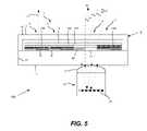
- FIG. 5is a cross section of one embodiment of the present invention.
- FIG. 6is a more detailed cross section of the embodiment of FIG. 5 ;
- FIG. 7is a cross section of an alternative embodiment of the present invention having transparent thin-film electronic components
- FIG. 8is a cross section of a further embodiment of the present invention having a plurality of transparent display pixels
- FIG. 9is a cross section of another embodiment of the present invention having a plurality of transparent display pixels of a common color
- FIG. 10is a cross section of yet another embodiment of the present invention having adjacent transparent portions
- FIG. 11is a top view of the embodiment of FIG. 10 ;
- FIG. 12is a cross section of an alternative embodiment of the present invention having common light-emitting materials and color filters;
- FIG. 13is a cross section of an additional embodiment of the present invention having an electrode with reflective and transparent portions;
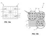
- FIG. 14Ais a top view of a further embodiment of the present invention having multiple transparent portions and image capture devices;
- FIG. 14Bis a top view of a display of the present invention depicting various exemplary groupings of the semi-transparent pixels
- FIG. 15is a cross section of an alternative embodiment of the present invention having Fourier plane spatial filtering
- FIG. 17is a top view showing system components of the present invention in one embodiment.
- FIG. 18is a block diagram showing system components of the present invention in a networked embodiment.
- the apparatus and method of the present inventionavoid the pitfalls of compound imaging, as was described earlier with reference to the examples of the Tsuboi '8332, Uy '7222, and Zanaty '0973 disclosures by using imaging optics and sensor components, rather than merely using sensors that detect light and attempting to assemble an image by tiling or other image synthesis methods.
- the apparatus and method of the present inventionavoid problems typically associated with pinhole imaging, as was described earlier with reference to the Rambo et al. '562, Ting '414, and Colmenarez et al. '866 disclosures. This is because the apparatus and method of the present invention utilize transparency properties of various types of display components to provide a suitable aperture for imaging, without significant detriment to display image quality.
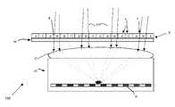
- FIGS. 2A and 2Bshow an important feature of operation that is utilized by the apparatus and method of the present invention.
- An integrated display and capture apparatus 100 of the present inventiongenerally includes a display 5 and one or more capture devices 40 .
- Display 5has an arrangement of pixel elements or pixels 8 and 9 that form a display screen that is observed by one or more viewers (not shown).
- Display pixels 8shown shaded in FIGS. 2A and 2B , are conventional display pixels, such as emissive OLED pixels or transmissive LCD pixels.
- Pixels 9shown white or clear in FIGS. 2A and 2B , also act as display pixels, but are fabricated and controlled to be at least partially transparent, and are thus termed as at least partially transparent (or semi-transparent) display pixels 9 in the present application.
- Capture device 40is nominally a digital or video camera having a lens 42 for directing light toward an image sensor 41 for capturing a plurality of image pixels.
- at least partially transparent pixels 9are in a display mode, contributing a portion of display image light 62 .
- Pixels 9either emit light (for an OLED display) or transmit (or reflect) light (for an LCD display).
- at least partially transparent pixels 9are in a transparent mode or clear mode, and receiving incident light 60 from a distant scene.
- the timing chart of FIG. 3shows a display timing pattern 102 for at least partially transparent pixels 9 and a capture timing pattern 104 for capturing an image from the image sensor 41 .
- a frame time ( ⁇ t)is spanned by one full cycle through ON and OFF states (an exemplary 50% duty cycle is shown).
- an image capture cyclecan be executed, as is shown in FIG. 2B .
- the at least partially transparent pixels 9are in a display state, nominally no image capture takes place.
- the timing patterns ( 106 a,b,c ) for the operation of the display pixels 8will be discussed subsequently.
- the capture device 40includes imaging optics with an optical axis 43 .
- the basic components of capture device 40are the lens 42 and an image sensor 41 , optionally encased in a housing 44 (shown in dotted lines in FIG. 4 ).
- Image sensor 41has an array of sensor pixels 45 , arranged in rows 46 and columns 47 , as is well known in the imaging arts.
- Incident light 60represented by dotted lines, is directed toward image sensor 41 by lens 42 to form an image thereon.
- Baffles (not shown) internal to lens 42can be provided to minimize any stray light or ghost images from degrading the image capture.
- Lens 42can employ folded optics the thickness of the housing.
- Image sensor 41can capture an image having a large number of pixels.
- Image sensor 41is likely a CCD or CMOS sensor array, having a resolution of ⁇ 1-8 megapixels.
- the image that is capturedcan be a full scene image or a portion or tile of a larger, composite image.
- the use of an image sensor 41 in the present inventionacts as a camera and provides a two-dimensional image from each capture device 40 .
- one embodiment of an integrated display and the capture apparatus 100includes display 5 having a plurality of display pixels 8 wherein one or more of the display pixels 8 is at least partially transparent (as shown by at least partially transparent display pixel 9 in FIG. 5 ) and partially opaque (as shown by display pixels 8 in FIG. 5 ).
- Capture device 40has an image sensor 41 for capturing a plurality of image pixels, as described earlier with reference to FIG. 4 .
- Display 5has a first side 6 from which it is viewed.
- Capture device 40is located on a second side 7 opposite the first side 6 , in a position corresponding to the location of the at least partially transparent display pixel 9 .
- Capture device 40receives light 60 from the scene on first side 6 through at least partially transparent pixel 9 to form an image of the scene.
- display 5is formed on a substrate 10 and includes a cover 20 adhered to the substrate 10 for protecting the display 5 .
- the first side 6 from which the display is viewedcan be the cover 20 side; second side 7 can be the substrate 10 side and the capture device 40 located adjacent to substrate 10 , with light emitted through cover 20 .
- display pixels 8include a reflective electrode 12 and a common transparent electrode 16 .
- Display pixels 8which can be either monochrome or color pixel, emit light in a forward direction (towards a display viewer), with the back-emitted light re-directed forwards by the reflective electrode 12 .
- the semi-transparent pixel 9 that is at least partially transparentcan include two transparent electrodes 16 and 13 .
- Thin film electronic components 30can be electrodes, transistors, resistors, or other basic circuitry components.
- a partially transparent pixelis one that transmits sufficient light to form an effective image when viewed or recorded by a capture device 40 .
- at least 50% transparencyis needed and better than 80% transparency is preferred.
- Transparencyis possible by virtue of device design and composition.
- OLED devicesbecause they use thin-film components, can be fabricated to be substantially transparent, as has been described in the article “Towards see-through displays: fully transparent thin-film transistors driving transparent organic light-emitting diodes,” by Gorrn et al., in Advanced Materials, 2006, 18(6), 738-741.
- the patterned materialsare deposited in thin films (e.g. 100 nm thick) that are effectively transparent.
- display pixels 8can include a layer 14 of patterned organic materials 14 R, 14 G, 14 B that emit red, green, or blue light respectively.
- display pixels 8 and semi-transparent pixels 9can both emit white light.
- OLED devicesare well known in the display imaging arts.
- layer 14includes switchable liquid crystals that switch between a transparent and a light-absorbing state.
- Reflective and transparent electrodesare known in the art and can include, for example, metals and metal oxides such as reflective aluminum or silver layers and transparent indium tin oxide conductors.
- Transparent electrodescan also be somewhat reflective, formed, for example, from thin layers of silver.
- LCD devicesare similarly well known in the display imaging arts. In particular, the general architecture of a trans-reflective LCD, in which the pixels have both reflective and transmissive portions could be extended to create an integrated display and capture device.
- transparent display pixel 9forms an aperture A in the display screen through which image sensor 41 obtains light 60 .
- the size of aperture A, or window, through which one or more capture devices look,is an important factor for the performance of the system. Optically, it is desirable that the size of the aperture A be as large as possible.
- An aperture Ashould be large enough (for example, >25 ⁇ m) that significant diffraction effects are not imparted to the light 60 in such a way that the image formed by the capture device 40 would be degraded.
- Increasing the size of aperture Aincreases the optical throughput of the light 60 available to a capture device 40 , enabling a brighter image with less noise.
- the relationship of aperture A to pixel sizeis important.
- pixel sizecan vary significantly between devices.
- the pixel sizecan be on the order of 0.05 to 1 mm 2 in area.
- current cell phone displaystypically have pixels that are ⁇ 0.1-0.2 mm wide, while computer monitors use ⁇ 0.3 mm wide pixel structures, and large panel entertainment systems have 0.5-0.8 mm wide pixel structures.
- the effective aperture size Ais increased with pixel structures in which regions of transparency are expanded by greater use of semi-transparent materials (such as ITO electrodes) or pixel patterning to enhance aperture adjacency.
- the effective aperture Ais increased by having image capture devices 40 look through multiple offset transparent pixels ( 9 ).
- the design of these apertures A of semi-transparent pixels (or ensembles thereof), including their size and patterning,needs to be designed with consideration for their visibility as potential display artifacts for a display user. Nominally the capture device 40 is aligned to be centered and normal (optical axis perpendicular to) an aperture A, unless it is deliberately askew, including being tilted or panned to track motion.
- display pixels 8are active-matrix pixels that include thin-film electronic components 30 to control the light emission or reflection of the display pixels.
- display 5has thin-film electronic components 30 are formed on substrate 10 .
- Planarization layers 32 and 34are employed to smooth layer surfaces and provide insulation between layers and between electrodes 12 and 13 formed in a common layer.
- the thin-film electronic componentsare formed on relatively opaque silicon.
- Electrode 13within aperture A, is transparent. Emitted light 62 can be provided from both transparent and opaque pixels.
- display 5has thin-film electronic components are formed of one or more transparent materials, for example zinc oxide or doped zinc oxide, and indium tin oxide (ITO).
- transparent materialsfor example zinc oxide or doped zinc oxide, and indium tin oxide (ITO).
- ITOindium tin oxide
- light 60can pass through any thin-film electronic components 30 which are “relatively transparent”, such as partially transparent electrodes 30 a , to be incident upon image sensor 41 .
- the size of semi-transparent pixelscan effectively be expanded, thereby increasing the aperture A size and improving the performance of the capture device 40 .
- the capture device 40receives light 60 through multiple display pixels 8 and 9 of display 5 , thereby increasing aperture A.
- some amount of lightis obtained from the imaged scene through the portion of light emitting pixel 14 W, including semi-transparent pixel 9 , and further light from the portion with a partially transparent electrode 30 a .
- Image lightis also collected through at least a portion of green color pixel 14 G, which is partially transparent layer of green patterned organic 14 G material in an OLED device.
- the aperture Acan be expanded further by providing other color-emitting pixels with a partially transparent electrode 30 a instead of a nominally opaque electrode ( 30 ).
- the partially transparent electrode 30 a of pixel 14 Wcan be of the light blocking variety ( 30 ).
- any semi-transmissive color pixels that are also functioning as windows for image captureshould be off (not light emitting) during the capture time.
- Various other spatial arrangements of partially transparent display pixels 9can be employed, with filtered or non-filtered light directed toward image sensor 41 , as is described subsequently.
- FIG. 9shows another embodiment for apparatus 100 in which light is obtained through an aperture A that comprises a plurality of offset or spaced apart window pixels that are interspersed among the display pixels.
- the depicted light transmitting or window pixelsare only at least partially transparent display pixels 9 .
- all of at least partially transparent display pixels 9emit the same color light, white in this case.
- the spaced apart light transmitting pixelscould be both white and color pixels, distributed individually or in clusters, to form aperture A. Since, with either OLED or LCD devices, different colors can have different light emission efficiencies, it can be useful to group commonly-colored transparent pixels to reduce differences between the differently colored pixel groups. In particular, white emitters can be more efficient than other colors. Using this improved efficiency can help to mitigate the visual impact of employing a non-reflective electrode.
- the effective aperture Acan be increased beyond that available through a single partially transparent display pixel 9 by fabricating the display 5 with the partially transparent display pixels 9 clustered or adjacent.
- the capture device 40can be larger and can thus receive more light, possibly increasing the signal of image sensor 41 .
- Reflected pixel layoutscan be arranged to accomplish this as taught in commonly assigned, above cited U.S. Ser. No. 11/341,945. Referring to FIG. 11 , a top view of a portion of display 5 having such an arrangement is shown.
- the component layoutemploys a bus connector 31 , thin-film transistors 30 b , and at least partially transparent pixels 9 located adjacent to each other to form an increased aperture A generally indicated by the dashed oval.
- the organic materialsdo not significantly absorb light that passes through the at least partially transparent display pixels 9 .
- the liquid crystalsare likewise substantially transparent.
- the capture device 40can employ additional color filters to form a color image of the scene on the first side 6 of the display 5 .
- an OLED embodiment of the present inventionemploying unpatterned organic materials 14 to form broadband light emitters together with color filters 24 R, 24 G, and 24 B to form a color display.
- the color filters 24 R, 24 G, and 24 Bcan significantly absorb light that passes through them, providing a colored image to capture device 40 . If an RGBW configuration is employed, the white emitter does not have any color filter. If capture device 40 is located in alignment with such a white pixel with no color filters, then the capture device 40 will not receive colored light. Hence, the capture device 40 can form a monochrome or a color image record without the need for separate color filters on image sensor 41 . An optional black matrix 22 can be employed to reduce ambient reflection.
- the color filters 24 R, 24 G, and 24 Bcan be located on the electrode as shown in FIG. 12 or on the inside of the protective cover 20 as shown in FIG. 7 .
- reflective electrode 12 of display 5can have a reflective area 12 a and a transparent area 13 a through which light passes to capture device 40 .
- a portion of the bottom electrodeis formed over areas corresponding to thin film electronic components 30 such as thin-film transistors, and another portion is formed for the areas between these thin-film components (transistors ( 30 )).
- Such an electrode structurecan be formed by providing a reflective, possibly conductive layer in the reflective areas 12 a only and a transparent layer over both the reflective areas 12 a and the transparent areas 13 a as shown in FIG. 13 .
- the display 5is controlled to emit or control light that forms a display image on the first side 6 of the display 5 , as was shown in FIG. 5 .
- Ambient light 60that illuminates a scene on the first side 6 is incident on the display 5 , passes through the one or more semi-transparent display pixels 9 , and is sensed by image sensor 41 of capture device 40 to form an image of the scene on the first side 9 .
- integrated display and capture apparatus 100can be equipped with one or more capture devices 40 that look through the display 5 .
- This plurality of capture devices (cameras) 40can have different imaging attributes, either individually or in combination.
- a lens for one camera 40can have zoom capability, while the other lenses do not.
- These cameras 40can have different numbers of pixels (different sensor resolutions), different spectral sensitivities of the light-sensing elements, different color filters, and other varying attributes.
- Some of these cameras 40can be mounted with means (not shown) to facilitate pan and tilt functionality, to enable motion tracking in the user/viewer scene environment.
- the plurality of capture devices 40can be directed to look at different parts of a scene, in an overlapping or a non-overlapping manner.
- An image processor 120can output either multiple images or multiple image data (video) streams, or composite images or composite image streams.
- a controller 122could facilitate both automatic and manual control of the variable features (zoom, pan, tilt, changing field of view, changing scene brightness, etc.) of the capture devices 40 to respond to changing scene conditions.
- the capture device 40can include a spectral filter 66 somewhere prior to image sensor 41 .
- spectral filter 66could be a band pass or band rejection filter.
- spectral filter 66could be a filter that transmits red and infrared light (600-1200 nm, for example) while rejecting ultraviolet, blue, green, and out of band infrared light.
- spectral filter 66could be a filter that preferentially transmits ultraviolet light.
- the associated image sensor 41will also need sufficient sensitivity in the chosen spectral range.
- a spectral filter 66can be used to eliminate light outside the region that is to be imaged.
- the inventionalso anticipates the need for capture devices 40 operating inside the visible spectrum to be combined with capture devices 40 operating outside the visible spectrum to enable sequential or simultaneous multi-spectral imaging.
- the integrated display and capture apparatus 100 of the present inventionincluding a display 5 with display pixels 8 and at least partially transparent pixels 9 , as well as one or more capture devices 40 , can be subject to image artifacts in either the image display or image capture spaces.
- image artifactsinclude spatial frequency effects, “screen door” effects, pin hole “defect” effects, stray and ghost light issues, color or spectral effects, flicker effects, and non-uniform shading issues.
- These artifacts (and others)which can occur individually or in combination, can generally be reduced with appropriate hardware designs or image processing corrections, which can likewise be applied individually or in combination.
- the goalwould be to reduce the presence of any image display or image capture artifacts to at least just below the appropriate threshold for human perception thereof, thereby enhancing the image quality.
- the hardware design and the image processingcan both be tailored to meet these needs.
- FIG. 15illustrates an integrated display and capture apparatus 100 that has baffles 64 to reduce image artifacts for both image display and image capture.
- Incident light 60passes through semi-transparent pixels 9 or display pixels 8 , and miss a given image capture device 40 . That light could enter the capture device 40 after various reflections and scattering events, and create ghost images or flare light, reducing image quality for either the displayed or captured images.
- Capture device 40can have an external housing 44 and internal baffles (not shown) that reduces this risk. Additionally, some incident light could re-emerge from behind the display 5 , through transparent pixels and display pixels 8 , and provide ghosts or flare light into the images seen by a viewer of the display.
- integrated display and capture apparatus 100is equipped with one or more light absorbing baffles 64 , which can include coated plates and surfaces, sheet polymer materials, or light trapping structures.
- Baffles 64can be formed on either side of substrate 10 of display 5 . It is noted that baffles 64 , which are similar to a backing for display 5 , are generally distinct from any thin film light absorbing layers that might be provided within the display micro-structure to reduce unintended stray reflections from incoming ambient light. With respect to FIG. 14 a , these baffles would be located behind display 5 , in the regions at least between the various image capture devices 40 . Of course, if semi-transparent pixels 9 are provided only in camera locations (see FIG. 14 a ), then baffles 64 may not be needed, or may only be need in proximity to apertures A.
- the integrated structure of integrated display and capture apparatus 100can cause various capture image artifacts, including shadowing.
- some portion of the light incident on image sensor 41may have been occluded by thin-film electronic components 30 in the optical path.
- the capture device 40records a scene with shadows imaged on image sensor 41 .
- Such shadowscan have a regular, periodic structure. Since these shadow areas are out of focus and are caused by a known part of the fixed optical structure of the digital capture device-display system, the effects of the shadows on the image can be modeled, tested, and compensated. Compensation techniques for ambient lighting conditions and for artifacts in the optics such as occlusions of the optical path are known and can be implemented in an image post-processing step. This step can be performed, for example, at image processor 120 , as shown in FIG. 18 .
- the structure of display 5can also cause other capture image defects, as image content is transmitted differently, removed, or obscured by the device structure.
- a light-transmitting aperture Acan span portions of semi-transparent pixels 14 W both with and without partially transparent electrodes 30 a , as well as portions color emitting pixels (such as 14 G) that can also be partially transparent, again either with or without partially transparent electrodes 30 a .
- these different partially transparent pixels or pixel portionscan have different transmittances in at least the blanking state, then the transmittance across an aperture A will vary spatially across the display 5 . As long as the objects in the captured scene are sufficiently distant from the display, these transmission variations should be averaged out for all field points.
- periodic spatial structures in display 5can cause capture image artifacts, where image content is removed, or obscured or altered by the effective frequencies of the structure.
- optical compensation or correction techniquescould be used.
- Fourier plane spatial filteringcan be used to reduce the visibility of artifacts caused by regular periodic structures.
- FIG. 15an integrated display and capture apparatus 100 is depicted in FIG. 15 , where display 5 has a repeating structure of red, green, blue and white pixels.
- Capture device 40which includes a lens 42 with multiple lens elements 42 a , 42 b and 42 c and an image sensor 41 , looks through a multitude of semi-transparent pixels 9 .
- the capture device 40may be looking through several, or several hundreds or more, of semi-transparent pixels 9 that are separated by color (or monochrome) pixels. Relative to the capture device 40 , imaging through this array of apertures formed by the semi-transparent pixels 9 can be much like imaging through a screen door, with a consequent loss of light intensity and the distraction of the structure itself, which can make focusing difficult, as well as impacting the image quality of scenes with similar spatial frequencies. Aliasing could also occur.
- These semi-transparent pixels 9can include white pixels (as in FIGS.
- semi-transparent structureswhere light is transmitted through nominally transparent electronic components (aperture A of FIG. 7 ) and/or through semi-transparent patterned color pixel structures (aperture A of FIG. 8 ).
- a static structurecan occur in frequency space.
- this frequency structureis evidenced in the Fourier plane of a lens system.
- capture device 40includes image sensor 41 and lens 42 with multiple lens elements ( 42 a , 42 b , and 42 c ).
- a Fourier plane 68exists, at, or in proximity to, an aperture stop 69 .
- Incident light 60which is incident from multiple locations in the field of view, is collected through semi-transparent pixels 9 and focused or converged towards the Fourier plane 68 (shown by a dashed line) and an aperture stop 69 , where after multiple lens elements 42 b and 42 c create images on image sensor 41 .
- spatial filtering with a fixed pattern Fourier plane filter 70can reduce the fixed or static spatial frequency patterns created by a display structure.
- this filtercan include a (two-dimensional) spatial pattern of highly absorbing regions formed on a transparent substrate, which is mounted between the multiple lens elements 42 a , 42 b and 42 c.
- the distribution or pattern of semi-transparent pixels 9 and apertures Acan also create display image artifacts that could affect the display viewer.
- these at least partially transparent pixel 9 structurescan be fairly large ( ⁇ 0.1-1.0 mm for a linear dimension) and patterned, they can create visible artifact that irritate the display user. For example, within an area with a pattern with different display intensities, the user can perceive a “banding effect”, where the structures appear as an artifact with a several mm pitch that aligns with regions of maximal human spatial pattern sensitivity.
- the pattern of semi-transparent pixel structurescan also create a speckled appearance to the display that could annoy the viewer.
- the pattern of window or transparent pixelscould seem like a grid of dark spots (in either a clear/transparent or dark state).
- FIG. 14 bin which different pixel groupings ( 26 a , 26 b , 26 c ) of semi-transparent pixels 9 are shown, and pixel groupings 26 a and 26 b represent regular grids. If the pixels 9 are small enough, they might exist generally un-noticed. However, as an example, the traverse of a displayed motion image across the display could increase their perceptibility for a viewer.
- the semi-transparent pixels 9can only be fabricated where cameras will be located, and not across an entire display.
- the semi-transparent pixels 9(white) can also be smaller than the RGB pixels.
- the semi-transparent pixels 9might be kept patterned in the same pitch within a row, but be staggered across rows, to appear less like a regular grid (less like pixel grouping 26 a ).
- display 5could have the intermingled semi-transparent pixels 9 (or apertures A) distributed quasi-periodically (pseudo-periodically) or randomly within a capture aperture of the capture device 40 , or more broadly, across different regions of the display 5 , to reduce this effect.
- These conceptsare exemplified by the illustrated pixel grouping 26 c of FIG. 12 b .
- electronic devices, and array electronic devices in particularare conventionally fabricated with predefined repeating structures, random pixelization would be quite difficult.
- a quasi-periodic structureis more likely, which could be either identical or non-identical in the XY directions (horizontal and vertical of FIG. 14 b ) of a display 5 .
- optical frequency spacefor image capture
- a quasi-periodic pattern of pixels 9could create a frequency pattern with gaussian profiles.
- Fourier plane filter 70could then have a spatial patterned absorbance that followed a functional dependence (such as a gaussian) in one or more locations, rather than the more traditional pattern of constant high absorbance (or reflectance) regions.
- frequency filtering to remove structural display artifacts from the image capturecould be done in the capture image processing electronics.
- optical filteringas compared to electrical/software filtering, is that it occurs without requiring any computing power for data processing.
- the timing diagram( FIG. 3 ) would be more complex, as the modulation within a frame time ( ⁇ t) would could be staggered (out of phase) or segmented from one pixel 9 to another. This modulation could change the apparent spatial pattern or frequency of these pixels as perceived by a viewer, whether the display 5 includes groupings ( 26 ) of semi-transparent pixels 9 that were periodically or quasi-periodically arrayed. In turn, that could affect the spatial frequency pattern seen at the Fourier plane 68 .
- Fourier plane filter 70could be a dynamic device, such as a spatial light modulator (such as an LCD or DMD) that was temporally modulated in synchronization with the modulation of pixels 9 .
- a spatial light modulatorsuch as an LCD or DMD
- synchronized frequency space correctionsare likely best handled directly in the image processor 120 that handle the captured images.
- semi-transparent pixels 9 or apertures Acan cause non-uniformity artifacts (in addition to flare) that will impact the displayed image, depending on whether these pixels appear dark or bright.
- the spatial distribution and size of semi-transparent pixels 9 across display 5very much affects these artifacts. Some of these issues are resolved if the dark state of semi-transparent pixels is a condition of both no light emission and no light transmission. However, there are still cases where display pixels 8 surrounding or adjacent to each of the semi-transparent pixels 9 (or apertures A) can be modulated in a calibrated compensating way to reduce the visibility of the semi-transparent pixels 9 to a viewer of the display.
- the display scene calibrationcan be undertaken in a scene dependent way, using the fact that the display electronics has information on the (static) structure of display 5 , has control of the pixel modulation timing and intensity, and can pre-process the image to be displayed. For example, when a semi-transparent pixel 9 is in a white state in an area where a generally bright whitish image is being displayed by the color pixels, the proximate display pixels 8 could be darkened to compensate. Likewise, when a semi-transparent pixel 9 (which can only be clear, dark, or white) resides in a displayed screen area of constant color content (say red), the adjacent display pixels 8 could be brightened to compensate for this pixel (as compared to red display pixels 8 further away from a semi-transparent pixel 9 ). In another sense, the semi-transparent pixels 9 might be used for display image contrast enhancement, given that they can be driven to either clear (dark) or white states.
- the application of local or adjacent display pixels 8 to compensate or correct for the operation of a semi-transparent pixel 9depends on how the display pixels are operated. For example, if non-transparent light emitting display pixels are on or emitting light during most of a frame time ⁇ t, then they are in operation for some portion (see display timing pattern 106 b of FIG. 3 ) of the clear state for image capture for a semi-transparent pixel 9 . The timing of display and capture is then at least somewhat de-coupled, although the defined frame time ⁇ t is presumed constant. Local changes in display pixel brightness can be attained by providing an average constant intensity or by actively changing the intensity within a frame time (display timing patterns 106 c of FIG. 3 ).
- adjacent or proximate display pixels neighboring a semi-transparent pixel 9could be driven higher when that pixel switches clear (for example, if the ensemble of proximate color pixels give a white image) or lower or left constant depending on the scene content.
- the ON or light emission state timing for the non-transparent light emitting display pixelsis comparable to that of the semi-transparent pixels 9 (display timing pattern 106 a ⁇ semi transparent pixel timing pattern 102 )
- display 5can be fabricated with semi-transparent pixels 9 or apertures A in places where capture devices 40 are present, or across the entire display 5 .
- the displayed imagescould look different in the capture regions versus the non-capture regions.
- these macro-non-uniformitiesshould be anticipated and correctable (perhaps with the help of a calibration step) in the image processing electronics 120 , and compensated for in advance of image display.
- semi-transparent pixels 9act as windows or apertures for image capture by one or more cameras 40 .
- these pixelscan be driven to an “ON”, light emitting state, to reduce their visibility to a display viewer.
- all the pixels within a cameras field of capturenominally need to be “OFF” or transparent for a sufficient time period that a nominally uniform image capture can occur over the capture field of view.
- the display state definition of a dark pixelcan be key. Generally, it is intended that a dark semi-transparent pixel 9 is still ON or in a display state, and does not transmit light to a capture device 40 .
- a dark statecan equate to an OFF/clear state, in which case incident light 60 can be transmitted to the capture device 40 .
- incident light 60can be transmitted to the capture device 40 .
- a semi-transparent pixelmight be left in its clear or transparent state (dark state for the display viewer) for a prolonged period of time (relative to the capture frame time), if it resides in an image region that is dark for a prolonged time period.
- Lightwould then be incident to the capture device (camera) 40 during the previously defined blank state.
- Capture device 40could have a shutter (not shown) to eliminate this concern.
- a spatially and/or temporally variant correction or gain adjustmentmight be made for the captured image as the prolonged dark semi-transparent pixels 9 within a cameras field of capture will have much more light transmission in time than the pixels that are reaching ON states.
- the simplest form of periodic controlcan be to switch the semi-transparent pixels 9 off (clear) for some portion of time to allow the capture device to capture the scene. Since, nominally, only the at least partially transparent display pixels 9 are switched rather than all of the pixels, the switching can be unobtrusive in the display. Moreover, the image capture can be made in a short portion of a period of time (e.g. 1/100 th of a second or a portion of a single frame at 30 Hz) reducing both the duty cycle for image capture and the visibility of temporal artifacts.
- the operation of non-transparent light emitting display pixelsis at least somewhat linked to the operation of the semi-transparent pixels 9 .
- Another image artifact, flickercan affect both image display and image capture devices.
- flickerby employing at least partially transparent display pixels 9 that switch between a non-active (transparent for image capture) and an active (ON) state, while the display pixels are active (emitting or reflecting) during most of the frame time, flicker is reduced relative to the image display. Since only the display pixels having at least partially transparent areas are switched between active and non-active states, the visual effect of the switching on the display quality is reduced and the user experience is improved.
- having display pixels on during image capturemeans that some display light can encounter objects in the capture field of view and reflect or scatter back towards the capture devices 40 . This light could raise the noise floor, change the spectrum, or temporally alter the captured images.
- image sensor 41back-emitted light (white or color) from the display 5 , for example in an OLED embodiment, with the reflective electrodes replaced by transmissive electrodes, can be incident on image sensor 41 .
- This issuecan largely be addressed by only emitting light from these window pixels with matched timing patterns 102 and 106 a of FIG. 3 .
- capture device 40can be equipped with a synchronized light blocking shutter or sensor drains. Alternately, it can be desirable to extend image capture (timing pattern 104 ′′) to occur while image display is occurring. That is, the window pixels (semi-transparent pixels 9 and semi-transparent color pixels (per FIG.
- the display controller 122knows the light 60 emitted by the display 5 , the light emission from the display 5 can be subtracted from the light signal received by image sensor 41 to improve the quality of image capture of the scene.
- the light emitted by the at least partially transparent display pixel 9can be periodically reduced during simultaneous image capture by image sensor 41 to improve the image capture of the scene.
- the amount of light absorbed by the partially transparent display pixel 9is likewise known to a display controller and a correction can be made to the corresponding image sensors to correct for the absorption of ambient light by the partially transparent display pixel 9 .
- integrated display and capture apparatus 100is an OLED type device and where at least partially transparent pixel 9 is then a light emitting pixel.
- integrated display and capture apparatus 100can also be a LCD type device. Even so, many of the previously discussed image artifacts, such as shadowing, flare light, spatial pattern frequency effects, spectral transmission differences, can affect the quality of the image capture. Likewise, many of the previously discussed image display artifacts, such as pixel pattern perception and local and macro brightness differences, can affect the quality of the image display.
- FIG. 1presents a typical prior art two-way telecommunication system is shown wherein the first viewer 71 views the first display 73 .
- a first image capture device 75which can be a digital camera, captures an image of the first viewer 71 .
- the display and capture apparatuswill be much more highly integrated than is implied by FIG. 1 .
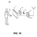
- FIG. 16shows, in block diagram form, an integrated display and capture apparatus 100 within part of a communications network.
- a viewer 80looks at display 5 that includes an integrated digital capture device 40 .
- Capture device 40obtains an image signal, as described subsequently, and provides the image signal to an image processor 86 that provides the image data for transmission to another site through a modulator 82 .
- a demodulator 84provides the controlling signals from the other site for operating display 5 .
- the block diagram of FIG. 17shows a top view of integrated display and capture apparatus 100 in an alternate embodiment having a control logic processor 90 and a communications module 92 for providing the image along a network 94 or 96 .
- FIG. 18shows a two-way communication system 110 that utilizes an integrated capture device and a display, for communication between a viewer 80 a at a first site 112 and a viewer 80 b at a second site 114 .
- Each viewer 80 a , 80 bhas an integrated image capture and display apparatus ( 100 ) comprising a display 5 with one or more integrated capture devices 40 .
- a central processing unit (CPU) 116coordinates control of the image processor 120 and the controller 122 that provides display driver and image capture control functions.
- a communication control apparatus 124acts as interface to a communication channel, such as a wireless or wired network channel, for transferring image and other data from one site to the other.
- a communication channelsuch as a wireless or wired network channel
- two-way communication system 110is optimized to support video conferencing.
- Each viewer 80 a , 80 bis able to see the other viewer displayed on display 5 at that site, enhancing human interaction for teleconferencing.
- Image processing electronics 120potentially serve multiple purposes, including improving the quality of image capture at the local display 5 , improving the quality of images displayed at the local display 5 , and handling the data for remote communication (by improving the image quality, data compression, encryption, etc.).
- FIG. 18shows a general arrangement of components that serve one embodiment. Capture devices 40 and display 5 are assembled into a frame or housing (not shown) as part of the device integration. This system housing can also encompass the image processor 120 , controller 122 , CPU 116 , and communication control 124 . Also not shown are audio communications and other support components that would also be used, as is well known in the video communications arts.
- the present inventionprovides an effective user experience as the capture device and display are naturally integrated in a mechanically thin package.
- the use of at least partially transparent display pixels 9 as opposed to pinholes formed in the displayimproves the fill factor or aperture ratio of the display, enabling more of the display area to emit or reflect light, thereby improving life times and display image quality. Display resolution can also be improved.
- the use of at least partially transparent display pixels 9 with the capture device 40 located behind the at least partially transparent display pixels 9allows the remainder of the display area to be reflective or light absorbing, thereby improving the amount of light output or reflected or improving the ambient contrast of the display, improving display image quality as a result. Forming multiple transparent areas improves the image capture capability by increasing the light available to capture devices 40 located behind the transparent areas or enabling a plurality of capture devices 40 to be employed.
- the integrated display and capture apparatus 100 of the present inventioncertainly has potential application for teleconferencing or video telephony. Additionally, this device might be used as an interpretive display for advertising or as an interactive display for video games and other entertainment formats.
- the displayed image contentcan include photographic images, animation, text, charts and graphs, diagrams, still and video materials, and other content, either individually or in combination.
- the integrated capture and display apparatus 100could be used to capture an image of one or more display users and then insert their images, in part or in total, into the displayed image content.
- Other applications for integrated display and capture apparatus 100in areas such as medical imaging, can be considered.
- Integrated display and capture apparatus 100can be sized for cell phone or handheld applications, or for use in a laptop or desktop computer, or for use in an entertainment display.
- Integrated display and capture apparatus 100can also be equipped with integrated light emitting devices for the purpose of illuminating a scene, which can be useful if the ambient lighting is low, or an unusual capture spectrum is desired.
- the illuminating devicesmight be places around the outer edges of display 5 .
- other optical sensing or detection devicescould be substituted for image sensor 41 in one or more capture devices 40 used with an integrated display and capture apparatus 100 .
- a low resolution wide angle lens and a quad cellwith simple sum and differencing electronics, could be used to track motion, such as recognizing that someone has entered the capture field of view.
- a specialized device, such as an optical fingerprint imagercould be provided, as a security feature.
- single cell sensorscould be used to detect ambient light levels or function as a photovoltaic cell for solar energy conversion. Most basically, an optical sensor needs to generate a useful electrical signal in response to incident light.
- the present inventioncan be employed in display devices. Such display devices can also include additional layers or optical devices, for example protective or encapsulating layers, filters, and polarizers e.g. circular polarizers.
- the present inventionis employed in a flat-panel OLED device composed of small molecule or polymeric OLEDs as disclosed in but not limited to U.S. Pat. No. 4,769,292, issued Sep. 6, 1988 to Tang et al., and U.S. Pat. No. 5,061,569, issued Oct. 29, 1991 to VanSlyke et al.
- organic light-emitting displayscan be used to fabricate such a device, including both active-matrix and passive-matrix OLED displays having either a top-emitter or bottom-emitter architecture.
- Other display device technologiescan also be used in the present invention, including devices based on inorganic phosphorescent materials, such as quantum dots.
Landscapes
- Chemical & Material Sciences (AREA)
- Inorganic Chemistry (AREA)
- Signal Processing (AREA)
- Sustainable Development (AREA)
- Engineering & Computer Science (AREA)
- Multimedia (AREA)
- Life Sciences & Earth Sciences (AREA)
- Control Of Indicators Other Than Cathode Ray Tubes (AREA)
- Devices For Indicating Variable Information By Combining Individual Elements (AREA)
- Blocking Light For Cameras (AREA)
- Stereoscopic And Panoramic Photography (AREA)
- Position Input By Displaying (AREA)
- Two-Way Televisions, Distribution Of Moving Picture Or The Like (AREA)
- Control Of El Displays (AREA)
Abstract
Description
- A aperture
- 5 display
- 6 first side
- 7 second side
- 8 display pixels
- 9 at least partially transparent display pixel (or semi-transparent pixel)
- 10 substrate
- 12 reflective electrode
- 12areflective area
- 13 transparent electrode
- 13atransparent area
- 14 organic layer
- 14R red patterned organic material
- 14G green patterned organic material
- 14B blue patterned organic material
- 14W white patterned organic material
- 16 transparent electrode
- 20 cover
- 22 black matrix
- 24R red color filter
- 24G green color filter
- 24B blue color filter
- 26 pixel groupings
- 26apixel grouping
- 26bpixel grouping
- 26cpixel grouping
- 30 thin-film electronic components
- 30apartially transparent electrodes
- 30bthin film transistors
- 31 bus connector
- 32 insulating planarization layer
- 34 insulating planarization layer
- 40 capture device (or camera)
- 41 image sensor
- 42 lens
- 42alens element
- 42blens element
- 42clens element
- 43 optical axis
- 44 housing
- 45 pixel
- 46 row
- 47 column
- 60 light
- 62 light
- 64 baffle
- 66 spectral filter
- 68 Fourier plane
- 69 Aperture stop
- 70 Fourier plane filter
- 71 first viewer
- 73 first Display
- 75 first image capture device
- 77 first still image memory
- 79 first D/A converter
- 80 viewer
- 80aviewer
- 80bviewer
- 81 first modulator/demodulator
- 82 modulator
- 83 first communication channel
- 84 demodulator
- 85 second viewer
- 86 image processor
- 87 second display
- 89 second image capture device
- 90 control logic processor
- 91 second still image memory
- 92 communications module
- 93 second D/A converter
- 94 network
- 95 second modulator/demodulator
- 96 network
- 97 second communication channel
- 100 integrated display and capture apparatus
- 102 semi-transparent pixel timing pattern
- 104 capture timing pattern
- 106adisplay timing pattern
- 106bdisplay timing pattern
- 106cdisplay timing pattern
- 110 two-way communication system
- 112 site
- 114 site
- 116 central processing unit (CPU)
- 120 image processor
- 122 controller
- 124 communication control apparatus
Claims (22)
Priority Applications (5)
| Application Number | Priority Date | Filing Date | Title |
|---|---|---|---|
| US11/555,822US7697053B2 (en) | 2006-11-02 | 2006-11-02 | Integrated display having multiple capture devices |
| PCT/US2007/022703WO2008057278A2 (en) | 2006-11-02 | 2007-10-26 | An integrated display having multiple capture devices |
| JP2009535284AJP2010509804A (en) | 2006-11-02 | 2007-10-26 | Integrated display with multiple capture devices |
| EP07852977AEP2084903A2 (en) | 2006-11-02 | 2007-10-26 | An integrated display having multiple capture devices |
| JP2013272243AJP2014098918A (en) | 2006-11-02 | 2013-12-27 | Integrated display having multiple capture devices |
Applications Claiming Priority (1)
| Application Number | Priority Date | Filing Date | Title |
|---|---|---|---|
| US11/555,822US7697053B2 (en) | 2006-11-02 | 2006-11-02 | Integrated display having multiple capture devices |
Publications (2)
| Publication Number | Publication Date |
|---|---|
| US20080106629A1 US20080106629A1 (en) | 2008-05-08 |
| US7697053B2true US7697053B2 (en) | 2010-04-13 |
Family
ID=39295530
Family Applications (1)
| Application Number | Title | Priority Date | Filing Date |
|---|---|---|---|
| US11/555,822Active2028-10-15US7697053B2 (en) | 2006-11-02 | 2006-11-02 | Integrated display having multiple capture devices |
Country Status (4)
| Country | Link |
|---|---|
| US (1) | US7697053B2 (en) |
| EP (1) | EP2084903A2 (en) |
| JP (2) | JP2010509804A (en) |
| WO (1) | WO2008057278A2 (en) |
Cited By (55)
| Publication number | Priority date | Publication date | Assignee | Title |
|---|---|---|---|---|
| US20070120879A1 (en)* | 2005-10-17 | 2007-05-31 | I2Ic Corporation | Combined Video Display and Camera System |
| US20080292151A1 (en)* | 2007-05-22 | 2008-11-27 | Kurtz Andrew F | Capturing data for individual physiological monitoring |
| US20090225502A1 (en)* | 2008-03-04 | 2009-09-10 | Qisda Corporation | Display Device |
| US20100188315A1 (en)* | 2009-01-23 | 2010-07-29 | Samsung Electronic Co . , Ltd ., | Electronic mirror and method for displaying image using the same |
| US20100314631A1 (en)* | 1998-01-27 | 2010-12-16 | Avistar Communications Corporation | Display-pixel and photosensor-element device and method therefor |
| US20110032369A1 (en)* | 2008-05-25 | 2011-02-10 | Avistar Communications Corporation | Vignetted optoelectronic array for use in synthetic image formation via signal processing, lensless cameras, and integrated camera-displays |
| US20110141079A1 (en)* | 2009-12-11 | 2011-06-16 | Canon Kabushiki Kaisha | Image display apparatus, control method thereof, and computer-readable storage medium |
| US20110181587A1 (en)* | 2010-01-22 | 2011-07-28 | Sony Corporation | Image display device having imaging device |
| US20120182437A1 (en)* | 2011-01-13 | 2012-07-19 | International Business Machines Corporation | Generating still images and video by capture of images projected by light passing through a display screen |
| US20120307123A1 (en)* | 2011-06-01 | 2012-12-06 | Cok Ronald S | Apparatus for displaying and sensing images |
| US20130088154A1 (en)* | 2010-06-17 | 2013-04-11 | High Tech Campus 5 | Display and lighting arrangement for a fitting room |
| US20130135328A1 (en)* | 2011-11-30 | 2013-05-30 | Apple Inc. | Devices and methods for providing access to internal component |
| US20140192023A1 (en)* | 2013-01-10 | 2014-07-10 | Samsung Display Co., Ltd. | Proximity and touch sensing surface for integration with a display |
| US8872985B2 (en) | 2012-04-13 | 2014-10-28 | Red.Com, Inc. | Video projector system |
| US9025086B2 (en) | 2012-04-13 | 2015-05-05 | Red.Com, Inc. | Video projector system |
| US9615054B1 (en) | 2014-09-25 | 2017-04-04 | Steve H. McNelley | Transparent communication devices |
| WO2017074881A1 (en)* | 2015-10-30 | 2017-05-04 | Essential Products, Inc. | Camera integrated into a display |
| WO2017074880A1 (en)* | 2015-10-30 | 2017-05-04 | Essential Products, Inc. | Camera integrated into a display |
| US9754526B2 (en) | 2015-10-30 | 2017-09-05 | Essential Products, Inc. | Mobile device with display overlaid with at least a light sensor |
| US9767728B2 (en) | 2015-10-30 | 2017-09-19 | Essential Products, Inc. | Light sensor beneath a dual-mode display |
| US9843736B2 (en) | 2016-02-26 | 2017-12-12 | Essential Products, Inc. | Image capture with a camera integrated display |
| US9848169B2 (en) | 2014-09-25 | 2017-12-19 | Steve H. McNelley | Transparent projection communication terminals |
| US9870024B2 (en) | 2015-10-30 | 2018-01-16 | Essential Products, Inc. | Camera integrated into a display |
| US9930290B2 (en) | 2014-09-25 | 2018-03-27 | Steve H. McNelley | Communication stage and integrated systems |
| US10055637B2 (en) | 2016-12-07 | 2018-08-21 | Synaptics Incorporated | Optical sensor with substrate light filter |
| US10102789B2 (en) | 2015-10-30 | 2018-10-16 | Essential Products, Inc. | Mobile device with display overlaid with at least a light sensor |
| US10115000B2 (en) | 2015-12-11 | 2018-10-30 | Synaptics Incorporated | Method and system for optical imaging using patterned illumination |
| US10129984B1 (en) | 2018-02-07 | 2018-11-13 | Lockheed Martin Corporation | Three-dimensional electronics distribution by geodesic faceting |
| US10129506B2 (en) | 2014-09-25 | 2018-11-13 | Steve H. McNelley | Advanced transparent projection communication terminals |
| US10147757B2 (en) | 2015-02-02 | 2018-12-04 | Synaptics Incorporated | Image sensor structures for fingerprint sensing |
| US10181070B2 (en) | 2015-02-02 | 2019-01-15 | Synaptics Incorporated | Low profile illumination in an optical fingerprint sensor |
| US10229316B2 (en) | 2016-01-29 | 2019-03-12 | Synaptics Incorporated | Compound collimating system using apertures and collimators |
| US10298877B2 (en) | 2014-09-25 | 2019-05-21 | Steve H. McNelley | Communication stage and display systems |
| US10510812B2 (en) | 2017-11-09 | 2019-12-17 | Lockheed Martin Corporation | Display-integrated infrared emitter and sensor structures |
| US10594951B2 (en) | 2018-02-07 | 2020-03-17 | Lockheed Martin Corporation | Distributed multi-aperture camera array |
| US10652529B2 (en) | 2018-02-07 | 2020-05-12 | Lockheed Martin Corporation | In-layer Signal processing |
| US10690910B2 (en) | 2018-02-07 | 2020-06-23 | Lockheed Martin Corporation | Plenoptic cellular vision correction |
| US10698201B1 (en) | 2019-04-02 | 2020-06-30 | Lockheed Martin Corporation | Plenoptic cellular axis redirection |
| US10705272B2 (en) | 2015-02-02 | 2020-07-07 | Will Semiconductor (Shanghai) Co., Ltd. | Optical fingerprint sensor |
| US10838468B2 (en)* | 2019-01-28 | 2020-11-17 | EMC IP Holding Company LLC | Mounting a camera behind a transparent organic light emitting diode (TOLED) display |
| US10838250B2 (en) | 2018-02-07 | 2020-11-17 | Lockheed Martin Corporation | Display assemblies with electronically emulated transparency |
| US10841535B2 (en) | 2014-09-25 | 2020-11-17 | Steve H. McNelley | Configured transparent communication terminals |
| US10866413B2 (en) | 2018-12-03 | 2020-12-15 | Lockheed Martin Corporation | Eccentric incident luminance pupil tracking |
| US10930709B2 (en) | 2017-10-03 | 2021-02-23 | Lockheed Martin Corporation | Stacked transparent pixel structures for image sensors |
| US10951883B2 (en) | 2018-02-07 | 2021-03-16 | Lockheed Martin Corporation | Distributed multi-screen array for high density display |
| US10979699B2 (en) | 2018-02-07 | 2021-04-13 | Lockheed Martin Corporation | Plenoptic cellular imaging system |
| US10986255B2 (en) | 2015-10-30 | 2021-04-20 | Essential Products, Inc. | Increasing display size by placing optical sensors beneath the display of an electronic device |
| US11055356B2 (en) | 2006-02-15 | 2021-07-06 | Kurtis John Ritchey | Mobile user borne brain activity data and surrounding environment data correlation system |
| US11099465B2 (en) | 2014-09-25 | 2021-08-24 | Steve H. McNelley | Communication stage and display systems |
| US11258983B2 (en) | 2014-09-25 | 2022-02-22 | Steve H. McNelley | Immersive communication terminals |
| US20220320183A1 (en)* | 2020-05-15 | 2022-10-06 | Chengdu Boe Optoelectronics Technology Co., Ltd. | Oled display substrate, method of manufacturing the same and oled display apparatus |
| US11594159B2 (en) | 2019-01-09 | 2023-02-28 | Dolby Laboratories Licensing Corporation | Display management with ambient light compensation |
| US11616941B2 (en) | 2018-02-07 | 2023-03-28 | Lockheed Martin Corporation | Direct camera-to-display system |
| US11637156B2 (en) | 2019-12-23 | 2023-04-25 | Lg Display Co., Ltd. | Pixel array substrate and display device including the same |
| US11750772B2 (en) | 2014-09-25 | 2023-09-05 | Steve H. McNelley | Rear illuminated transparent communication terminals |
Families Citing this family (97)
| Publication number | Priority date | Publication date | Assignee | Title |
|---|---|---|---|---|
| US20080316348A1 (en)* | 2007-06-21 | 2008-12-25 | Cisco Technology, Inc. | Virtual whiteboard |
| US20090119593A1 (en)* | 2007-11-01 | 2009-05-07 | Cisco Technology, Inc. | Virtual table |
| US8769437B2 (en)* | 2007-12-12 | 2014-07-01 | Nokia Corporation | Method, apparatus and computer program product for displaying virtual media items in a visual media |
| JP5116514B2 (en)* | 2008-03-11 | 2013-01-09 | キヤノン株式会社 | Imaging apparatus and display control method |
| JP5246490B2 (en)* | 2008-08-29 | 2013-07-24 | ソニー株式会社 | Input/Output Devices |
| JP5235798B2 (en)* | 2009-06-22 | 2013-07-10 | 富士フイルム株式会社 | Imaging apparatus and control method thereof |
| US9900150B2 (en)* | 2009-10-30 | 2018-02-20 | International Business Machines Corporation | Dispersed storage camera device and method of operation |
| JP5533039B2 (en)* | 2009-11-02 | 2014-06-25 | ソニー株式会社 | Image display device with imaging device |
| JP2011150583A (en)* | 2010-01-22 | 2011-08-04 | Sony Corp | Image display device having imaging device |
| US8587682B2 (en)* | 2010-02-12 | 2013-11-19 | Nvidia Corporation | Display system, method, and computer program product for capturing images using multiple integrated image sensors |
| KR101640456B1 (en)* | 2010-03-15 | 2016-07-19 | 삼성전자주식회사 | Apparatus and Method imaging through hole of each pixels of display panel |
| JP2011242616A (en)* | 2010-05-19 | 2011-12-01 | Sony Corp | Image display device, electronic apparatus, image display system, image acquisition method, and program |
| US20110292213A1 (en)* | 2010-05-26 | 2011-12-01 | Lacey James H | Door mountable camera surveillance device and method |
| KR101725044B1 (en)* | 2010-05-27 | 2017-04-11 | 삼성전자주식회사 | Imaging display apparatus |
| JP5743048B2 (en)* | 2010-06-22 | 2015-07-01 | 株式会社Joled | Image display device, electronic device, image display system, image display method, and program |
| KR101781533B1 (en)* | 2010-12-23 | 2017-09-27 | 삼성디스플레이 주식회사 | Image capture apparatus and photographing method using the apparatus |
| KR20120080845A (en)* | 2011-01-10 | 2012-07-18 | 삼성전자주식회사 | Oled display apparatus having optical sensing funtion |
| KR101929561B1 (en)* | 2012-03-20 | 2018-12-18 | 삼성전자주식회사 | Display apparatus for supporting field of view control |
| EP2658250A1 (en)* | 2012-04-26 | 2013-10-30 | Sony Mobile Communications AB | Screen camera |
| CN112911252B (en) | 2012-11-28 | 2023-07-04 | 核心光电有限公司 | Multi-aperture imaging system |
| US10257506B2 (en)* | 2012-12-28 | 2019-04-09 | Samsung Electronics Co., Ltd. | Method of obtaining depth information and display apparatus |
| KR101634516B1 (en) | 2013-06-13 | 2016-06-28 | 코어포토닉스 리미티드 | Dual aperture zoom digital camera |
| JP2016523389A (en) | 2013-07-04 | 2016-08-08 | コアフォトニクス リミテッド | Compact telephoto lens assembly |
| CN108989649B (en) | 2013-08-01 | 2021-03-19 | 核心光电有限公司 | Slim multi-aperture imaging system with autofocus and method of use |
| US9392188B2 (en) | 2014-08-10 | 2016-07-12 | Corephotonics Ltd. | Zoom dual-aperture camera with folded lens |
| EP3016381A1 (en)* | 2014-10-31 | 2016-05-04 | Thomson Licensing | Video conferencing system |
| CN112433331B (en) | 2015-01-03 | 2022-07-08 | 核心光电有限公司 | Miniature telephoto lens module and camera using the same |
| JP6429640B2 (en)* | 2015-01-21 | 2018-11-28 | キヤノン株式会社 | Communication system used in remote communication |
| US10360431B2 (en)* | 2015-03-25 | 2019-07-23 | Apple Inc. | Electronic device including pin hole array mask above optical image sensor and related methods |
| CN112394467B (en) | 2015-04-16 | 2023-06-09 | 核心光电有限公司 | Autofocus and Optical Image Stabilization in a Compact Folding Camera |
| US9699405B2 (en)* | 2015-07-14 | 2017-07-04 | Google Inc. | Immersive teleconferencing with translucent video stream |
| US10230898B2 (en) | 2015-08-13 | 2019-03-12 | Corephotonics Ltd. | Dual aperture zoom camera with video support and switching / non-switching dynamic control |
| WO2017058473A1 (en) | 2015-09-30 | 2017-04-06 | Cressputi Research Llc | Finger biometric sensor for generating three dimensional fingerprint ridge data and related methods |
| KR102369223B1 (en) | 2015-12-29 | 2022-03-02 | 코어포토닉스 리미티드 | Dual-aperture zoom digital camera with automatic adjustable tele field of view |
| WO2017164680A1 (en)* | 2016-03-24 | 2017-09-28 | 삼성전자주식회사 | Electronic device having display |
| CN109074475B (en) | 2016-05-23 | 2022-03-01 | 苹果公司 | Electronic device including pinhole array mask and related methods |
| US11239275B2 (en) | 2016-05-23 | 2022-02-01 | Apple Inc. | Electronic device including processing circuitry for sensing images from spaced apart sub-arrays and related methods |
| KR102002718B1 (en) | 2016-05-30 | 2019-10-18 | 코어포토닉스 리미티드 | Rotary Ball-Guid Voice Coil Motor |
| KR20240036133A (en) | 2016-06-19 | 2024-03-19 | 코어포토닉스 리미티드 | Frame synchronization in a dual-aperture camera system |
| KR20240051317A (en) | 2016-07-07 | 2024-04-19 | 코어포토닉스 리미티드 | Linear ball guided voice coil motor for folded optic |
| US20210319197A1 (en)* | 2016-11-15 | 2021-10-14 | Bidirectional Display Inc. | Apparatus and method for optically capturing fingerprint or other images on display screen |
| EP3842853B1 (en) | 2016-12-28 | 2024-03-06 | Corephotonics Ltd. | Folded camera structure with an extended light-folding-element scanning range |
| US10884321B2 (en) | 2017-01-12 | 2021-01-05 | Corephotonics Ltd. | Compact folded camera |
| CN106603772B (en)* | 2017-01-26 | 2019-12-27 | Oppo广东移动通信有限公司 | Electronic device and image acquisition method |
| KR102530535B1 (en) | 2017-03-15 | 2023-05-08 | 코어포토닉스 리미티드 | Cameras with panoramic scanning range |
| WO2019048904A1 (en) | 2017-09-06 | 2019-03-14 | Corephotonics Ltd. | Combined stereoscopic and phase detection depth mapping in a dual aperture camera |
| JP6897442B2 (en)* | 2017-09-12 | 2021-06-30 | 株式会社Jvcケンウッド | Vehicle equipment, calibration result determination system, calibration result determination method, and program |
| US10951834B2 (en) | 2017-10-03 | 2021-03-16 | Corephotonics Ltd. | Synthetically enlarged camera aperture |
| KR101976831B1 (en)* | 2017-10-31 | 2019-05-10 | 엘지디스플레이 주식회사 | Personal immersion apparatus |
| US11333955B2 (en) | 2017-11-23 | 2022-05-17 | Corephotonics Ltd. | Compact folded camera structure |
| CN110033699A (en)* | 2018-01-12 | 2019-07-19 | 京东方科技集团股份有限公司 | Display base plate and preparation method thereof, display device |
| CN114609746A (en) | 2018-02-05 | 2022-06-10 | 核心光电有限公司 | Folding camera device |
| CN113568251B (en) | 2018-02-12 | 2022-08-30 | 核心光电有限公司 | Digital camera and method for providing focus and compensating for camera tilt |
| US10694168B2 (en) | 2018-04-22 | 2020-06-23 | Corephotonics Ltd. | System and method for mitigating or preventing eye damage from structured light IR/NIR projector systems |
| KR20250053984A (en) | 2018-04-23 | 2025-04-22 | 코어포토닉스 리미티드 | An optical-path folding-element with an extended two degree of freedom rotation range |
| KR102025012B1 (en)* | 2018-05-08 | 2019-09-24 | 재단법인 다차원 스마트 아이티 융합시스템 연구단 | Multi pixel micro lens pixel array and camera system for solving color mix and operating method thereof |
| WO2019213839A1 (en) | 2018-05-08 | 2019-11-14 | Guangdong Oppo Mobile Telecommunications Corp., Ltd. | Terminal device and image capturing method |
| CN119919618A (en) | 2018-07-04 | 2025-05-02 | 核心光电有限公司 | Cameras with folded scanning beam path for automotive or surveillance applications |
| CN108919573B (en)* | 2018-07-13 | 2019-12-20 | 京东方科技集团股份有限公司 | Display panel, display device, imaging method and depth distance detection method |
| CN109067942B (en)* | 2018-08-03 | 2021-03-16 | Oppo广东移动通信有限公司 | Display screen and electronic device with same |
| CN111316346B (en)* | 2018-08-04 | 2022-11-29 | 核心光电有限公司 | Switchable continuous display information system above camera |
| US11635596B2 (en) | 2018-08-22 | 2023-04-25 | Corephotonics Ltd. | Two-state zoom folded camera |
| CN110969982B (en)* | 2018-09-28 | 2022-09-13 | 北京小米移动软件有限公司 | Display structure, display panel and display device |
| CN109308866A (en)* | 2018-10-26 | 2019-02-05 | 武汉华星光电半导体显示技术有限公司 | an electronic device |
| KR102648723B1 (en) | 2018-12-31 | 2024-03-18 | 삼성디스플레이 주식회사 | Display device and driving method thereof |
| US11287081B2 (en) | 2019-01-07 | 2022-03-29 | Corephotonics Ltd. | Rotation mechanism with sliding joint |
| CN111524932A (en)* | 2019-02-01 | 2020-08-11 | Oppo广东移动通信有限公司 | Electronic equipment, pixel structure and display device |
| EP3907556B1 (en)* | 2019-02-01 | 2024-04-03 | Guangdong Oppo Mobile Telecommunications Corp., Ltd. | Electronic device and display apparatus |
| KR102770831B1 (en)* | 2019-02-07 | 2025-02-24 | 삼성디스플레이 주식회사 | Display apparatus |
| EP4224841B1 (en) | 2019-03-09 | 2025-06-25 | Corephotonics Ltd. | Method for dynamic stereoscopic calibration |
| US11516374B2 (en)* | 2019-06-05 | 2022-11-29 | Synaptics Incorporated | Under-display image sensor |
| KR102827226B1 (en)* | 2019-06-19 | 2025-07-01 | 삼성전자주식회사 | An electronic device including a display formed a random pattern |
| WO2021015790A1 (en)* | 2019-07-25 | 2021-01-28 | Hewlett-Packard Development Company, L.P. | Displays with partial transparent areas |
| US11368631B1 (en) | 2019-07-31 | 2022-06-21 | Corephotonics Ltd. | System and method for creating background blur in camera panning or motion |
| CN112736111B (en)* | 2019-10-29 | 2025-08-15 | 北京小米移动软件有限公司 | Screen module and electronic equipment |
| US11659135B2 (en) | 2019-10-30 | 2023-05-23 | Corephotonics Ltd. | Slow or fast motion video using depth information |
| KR20210069289A (en)* | 2019-12-03 | 2021-06-11 | 엘지디스플레이 주식회사 | Display device |
| US11949976B2 (en) | 2019-12-09 | 2024-04-02 | Corephotonics Ltd. | Systems and methods for obtaining a smart panoramic image |
| CN114641983A (en) | 2019-12-09 | 2022-06-17 | 核心光电有限公司 | System and method for obtaining intelligent panoramic image |
| CN111062991B (en)* | 2019-12-27 | 2023-05-05 | 西安因诺航空科技有限公司 | Method and device for positioning inspection target of photovoltaic scene and readable storage medium |
| KR102714525B1 (en)* | 2019-12-30 | 2024-10-07 | 엘지디스플레이 주식회사 | Display apparatus |
| EP4546027A3 (en) | 2020-02-22 | 2025-08-13 | Corephotonics Ltd. | Split screen feature for macro photography |
| EP4097773A4 (en) | 2020-04-26 | 2023-11-01 | Corephotonics Ltd. | TEMPERATURE CONTROL FOR HALL BAR SENSOR CORRECTION |
| CN117372249A (en) | 2020-05-17 | 2024-01-09 | 核心光电有限公司 | Image stitching of full field of view reference images |
| US11770609B2 (en) | 2020-05-30 | 2023-09-26 | Corephotonics Ltd. | Systems and methods for obtaining a super macro image |
| KR102862382B1 (en) | 2020-07-15 | 2025-09-18 | 코어포토닉스 리미티드 | Point of view aberrations correction in a scanning folded camera |
| US11637977B2 (en) | 2020-07-15 | 2023-04-25 | Corephotonics Ltd. | Image sensors and sensing methods to obtain time-of-flight and phase detection information |
| CN118433505A (en) | 2020-07-31 | 2024-08-02 | 核心光电有限公司 | camera |
| WO2022034402A1 (en) | 2020-08-12 | 2022-02-17 | Corephotonics Ltd. | Optical image stabilization in a scanning folded camera |
| CN114078365A (en)* | 2020-08-18 | 2022-02-22 | 群创光电股份有限公司 | Display device and driving method thereof |
| US11509806B2 (en)* | 2020-10-13 | 2022-11-22 | Qualcomm Incorporated | Under-display camera synchronization with display pixel operation |
| KR102696960B1 (en) | 2020-12-26 | 2024-08-19 | 코어포토닉스 리미티드 | Video support in a multi-aperture mobile camera with a scanning zoom camera |
| US11706517B2 (en)* | 2021-03-10 | 2023-07-18 | Google Llc | Vertically long apertures for computing device cameras |
| KR102589548B1 (en) | 2021-03-11 | 2023-10-13 | 코어포토닉스 리미티드 | Pop-out camera system |
| US12007671B2 (en) | 2021-06-08 | 2024-06-11 | Corephotonics Ltd. | Systems and cameras for tilting a focal plane of a super-macro image |
| US12328505B2 (en) | 2022-03-24 | 2025-06-10 | Corephotonics Ltd. | Slim compact lens optical image stabilization |
| TWI824770B (en)* | 2022-10-13 | 2023-12-01 | 財團法人工業技術研究院 | Display element and projector |
Citations (25)
| Publication number | Priority date | Publication date | Assignee | Title |
|---|---|---|---|---|
| US4769292A (en) | 1987-03-02 | 1988-09-06 | Eastman Kodak Company | Electroluminescent device with modified thin film luminescent zone |
| US4928301A (en) | 1988-12-30 | 1990-05-22 | Bell Communications Research, Inc. | Teleconferencing terminal with camera behind display screen |
| US5061569A (en) | 1990-07-26 | 1991-10-29 | Eastman Kodak Company | Electroluminescent device with organic electroluminescent medium |
| US5159445A (en)* | 1990-12-31 | 1992-10-27 | At&T Bell Laboratories | Teleconferencing video display system for improving eye contact |
| US5194955A (en) | 1990-05-19 | 1993-03-16 | Sony Corporation | Video telephone |
| GB2273411A (en)* | 1992-12-11 | 1994-06-15 | Ibm | Video conferencing terminal |
| US5585817A (en)* | 1992-05-20 | 1996-12-17 | Sharp Kabushiki Kaisha | Apparatus and a method for inputting/outputting an image |
| US5639151A (en) | 1996-02-16 | 1997-06-17 | Mcnelley; Steve H. | Pass-through reflective projection display |
| US5777665A (en) | 1995-09-20 | 1998-07-07 | Videotronic Systems | Image blocking teleconferencing eye contact terminal |
| EP1209901A1 (en) | 2000-11-22 | 2002-05-29 | Deutsche Thomson-Brandt Gmbh | Image pick-up and display apparatus |
| US6454414B1 (en) | 2000-05-24 | 2002-09-24 | Chi Mei Optoelectronics Corporation | Device for image output and input |
| US6473238B1 (en)* | 2000-03-17 | 2002-10-29 | Stephen Daniell | Lens arrays |
| US20030071932A1 (en)* | 2000-02-22 | 2003-04-17 | Yasushi Tanigaki | Image displaying and picking-up device |
| US20040140973A1 (en) | 2003-01-16 | 2004-07-22 | Zanaty Farouk M. | System and method of a video capture monitor concurrently displaying and capturing video images |
| US6771303B2 (en) | 2002-04-23 | 2004-08-03 | Microsoft Corporation | Video-teleconferencing system with eye-gaze correction |
| US20040196360A1 (en) | 2000-11-29 | 2004-10-07 | Hillis W. Daniel | Method and apparatus maintaining eye contact in video delivery systems using view morphing |
| US20040263670A1 (en)* | 2003-06-18 | 2004-12-30 | Ryo Yamasaki | Display device with image sensing device |
| US20050024489A1 (en) | 1999-11-30 | 2005-02-03 | Eastman Kodak Company | Image capture and display device |
| US6888562B2 (en) | 2003-03-26 | 2005-05-03 | Broadcom Corporation | Integral eye-path alignment on telephony and computer video devices using a pinhole image sensing device |
| EP1536399A1 (en) | 2003-11-26 | 2005-06-01 | Barco N.V. | Method and device for visual masking of defects in matrix displays by using characteristics of the human vision system |
| US20050128332A1 (en)* | 2003-12-12 | 2005-06-16 | Takayuki Tsuboi | Display apparatus with camera and communication apparatus |
| US20060007222A1 (en) | 2004-06-21 | 2006-01-12 | Apple Computer, Inc. | Integrated sensing display |
| US7034866B1 (en) | 2000-11-22 | 2006-04-25 | Koninklijke Philips Electronics N.V. | Combined display-camera for an image processing system |
| US7042486B2 (en) | 1999-11-30 | 2006-05-09 | Eastman Kodak Company | Image capture and display device |
| US20070002130A1 (en)* | 2005-06-21 | 2007-01-04 | David Hartkop | Method and apparatus for maintaining eye contact during person-to-person video telecommunication |
Family Cites Families (7)
| Publication number | Priority date | Publication date | Assignee | Title |
|---|---|---|---|---|
| JPS62258574A (en)* | 1986-05-02 | 1987-11-11 | Fujitsu Ltd | Time division display image pickup system |
| JPH06217298A (en)* | 1993-01-13 | 1994-08-05 | Oki Electric Ind Co Ltd | Visual telephone set |
| JPH07143469A (en)* | 1993-11-12 | 1995-06-02 | Hitachi Denshi Ltd | Imaging display integrated device |
| JPH08195945A (en)* | 1995-01-17 | 1996-07-30 | Japan Aviation Electron Ind Ltd | Display device with camera |
| JP2003185988A (en)* | 2001-12-17 | 2003-07-03 | Sumitomo Electric Ind Ltd | Display device provided with imaging device, terminal device including the display device, and interactive interactive system |
| JP4515161B2 (en)* | 2003-06-17 | 2010-07-28 | 株式会社半導体エネルギー研究所 | Display device with imaging function and bidirectional communication system |
| JP4178089B2 (en)* | 2003-09-18 | 2008-11-12 | 富士フイルム株式会社 | Imaging display device |
- 2006
- 2006-11-02USUS11/555,822patent/US7697053B2/enactiveActive
- 2007
- 2007-10-26WOPCT/US2007/022703patent/WO2008057278A2/enactiveApplication Filing
- 2007-10-26EPEP07852977Apatent/EP2084903A2/ennot_activeCeased
- 2007-10-26JPJP2009535284Apatent/JP2010509804A/ennot_activeWithdrawn
- 2013
- 2013-12-27JPJP2013272243Apatent/JP2014098918A/enactivePending
Patent Citations (25)
| Publication number | Priority date | Publication date | Assignee | Title |
|---|---|---|---|---|
| US4769292A (en) | 1987-03-02 | 1988-09-06 | Eastman Kodak Company | Electroluminescent device with modified thin film luminescent zone |
| US4928301A (en) | 1988-12-30 | 1990-05-22 | Bell Communications Research, Inc. | Teleconferencing terminal with camera behind display screen |
| US5194955A (en) | 1990-05-19 | 1993-03-16 | Sony Corporation | Video telephone |
| US5061569A (en) | 1990-07-26 | 1991-10-29 | Eastman Kodak Company | Electroluminescent device with organic electroluminescent medium |
| US5159445A (en)* | 1990-12-31 | 1992-10-27 | At&T Bell Laboratories | Teleconferencing video display system for improving eye contact |
| US5585817A (en)* | 1992-05-20 | 1996-12-17 | Sharp Kabushiki Kaisha | Apparatus and a method for inputting/outputting an image |
| GB2273411A (en)* | 1992-12-11 | 1994-06-15 | Ibm | Video conferencing terminal |
| US5777665A (en) | 1995-09-20 | 1998-07-07 | Videotronic Systems | Image blocking teleconferencing eye contact terminal |
| US5639151A (en) | 1996-02-16 | 1997-06-17 | Mcnelley; Steve H. | Pass-through reflective projection display |
| US7042486B2 (en) | 1999-11-30 | 2006-05-09 | Eastman Kodak Company | Image capture and display device |
| US20050024489A1 (en) | 1999-11-30 | 2005-02-03 | Eastman Kodak Company | Image capture and display device |
| US20030071932A1 (en)* | 2000-02-22 | 2003-04-17 | Yasushi Tanigaki | Image displaying and picking-up device |
| US6473238B1 (en)* | 2000-03-17 | 2002-10-29 | Stephen Daniell | Lens arrays |
| US6454414B1 (en) | 2000-05-24 | 2002-09-24 | Chi Mei Optoelectronics Corporation | Device for image output and input |
| US7034866B1 (en) | 2000-11-22 | 2006-04-25 | Koninklijke Philips Electronics N.V. | Combined display-camera for an image processing system |
| EP1209901A1 (en) | 2000-11-22 | 2002-05-29 | Deutsche Thomson-Brandt Gmbh | Image pick-up and display apparatus |
| US20040196360A1 (en) | 2000-11-29 | 2004-10-07 | Hillis W. Daniel | Method and apparatus maintaining eye contact in video delivery systems using view morphing |
| US6771303B2 (en) | 2002-04-23 | 2004-08-03 | Microsoft Corporation | Video-teleconferencing system with eye-gaze correction |
| US20040140973A1 (en) | 2003-01-16 | 2004-07-22 | Zanaty Farouk M. | System and method of a video capture monitor concurrently displaying and capturing video images |
| US6888562B2 (en) | 2003-03-26 | 2005-05-03 | Broadcom Corporation | Integral eye-path alignment on telephony and computer video devices using a pinhole image sensing device |
| US20040263670A1 (en)* | 2003-06-18 | 2004-12-30 | Ryo Yamasaki | Display device with image sensing device |
| EP1536399A1 (en) | 2003-11-26 | 2005-06-01 | Barco N.V. | Method and device for visual masking of defects in matrix displays by using characteristics of the human vision system |
| US20050128332A1 (en)* | 2003-12-12 | 2005-06-16 | Takayuki Tsuboi | Display apparatus with camera and communication apparatus |
| US20060007222A1 (en) | 2004-06-21 | 2006-01-12 | Apple Computer, Inc. | Integrated sensing display |
| US20070002130A1 (en)* | 2005-06-21 | 2007-01-04 | David Hartkop | Method and apparatus for maintaining eye contact during person-to-person video telecommunication |
Non-Patent Citations (1)
| Title |
|---|
| Gorrn et al, Towards see-thorugh displays: fully transparent thin-film transistors driving transparent organic light-emitting diodes, Adv. Mat. 2006 18(6) 738-741. |
Cited By (90)
| Publication number | Priority date | Publication date | Assignee | Title |
|---|---|---|---|---|
| US20100314631A1 (en)* | 1998-01-27 | 2010-12-16 | Avistar Communications Corporation | Display-pixel and photosensor-element device and method therefor |
| US8022977B2 (en)* | 2005-10-17 | 2011-09-20 | I2Ic Corporation | Camera placed behind a display with a transparent backlight |
| US20070120879A1 (en)* | 2005-10-17 | 2007-05-31 | I2Ic Corporation | Combined Video Display and Camera System |
| US8345129B2 (en)* | 2005-10-17 | 2013-01-01 | I2Ic Corporation | Camera placed behind a display with a transparent backlight |
| US20110292255A1 (en)* | 2005-10-17 | 2011-12-01 | I2Ic Corporation | Camera placed behind a display with a transparent backlight |
| US11055356B2 (en) | 2006-02-15 | 2021-07-06 | Kurtis John Ritchey | Mobile user borne brain activity data and surrounding environment data correlation system |
| US8831299B2 (en) | 2007-05-22 | 2014-09-09 | Intellectual Ventures Fund 83 Llc | Capturing data for individual physiological monitoring |
| US20080292151A1 (en)* | 2007-05-22 | 2008-11-27 | Kurtz Andrew F | Capturing data for individual physiological monitoring |
| US9298883B2 (en) | 2007-05-22 | 2016-03-29 | Intellectual Ventures Fund 83 Llc | Capturing data for individual physiological monitoring |
| US10192033B2 (en) | 2007-05-22 | 2019-01-29 | Monument Peak Ventures, Llc | Capturing data for individual physiological monitoring |
| US20090225502A1 (en)* | 2008-03-04 | 2009-09-10 | Qisda Corporation | Display Device |
| US20110032369A1 (en)* | 2008-05-25 | 2011-02-10 | Avistar Communications Corporation | Vignetted optoelectronic array for use in synthetic image formation via signal processing, lensless cameras, and integrated camera-displays |
| US8830375B2 (en)* | 2008-05-25 | 2014-09-09 | Lester F. Ludwig | Vignetted optoelectronic array for use in synthetic image formation via signal processing, lensless cameras, and integrated camera-displays |
| US9163994B2 (en)* | 2009-01-23 | 2015-10-20 | Samsung Electronics Co., Ltd. | Electronic mirror and method for displaying image using the same |
| US20100188315A1 (en)* | 2009-01-23 | 2010-07-29 | Samsung Electronic Co . , Ltd ., | Electronic mirror and method for displaying image using the same |
| US20110141079A1 (en)* | 2009-12-11 | 2011-06-16 | Canon Kabushiki Kaisha | Image display apparatus, control method thereof, and computer-readable storage medium |
| US8531444B2 (en)* | 2009-12-11 | 2013-09-10 | Canon Kabushiki Kaisha | Image display apparatus, control method thereof, and computer-readable storage medium |
| US20110181587A1 (en)* | 2010-01-22 | 2011-07-28 | Sony Corporation | Image display device having imaging device |
| US20130278646A1 (en)* | 2010-01-22 | 2013-10-24 | Sony Corporation | Image display device having imaging device |
| US20130088154A1 (en)* | 2010-06-17 | 2013-04-11 | High Tech Campus 5 | Display and lighting arrangement for a fitting room |
| US9357613B2 (en)* | 2010-06-17 | 2016-05-31 | Koninklijke Philips N.V. | Display and lighting arrangement for a fitting room |
| US8576325B2 (en)* | 2011-01-13 | 2013-11-05 | International Business Machines Corporation | Generating still images and video by capture of images projected by light passing through a display screen |
| US20120182437A1 (en)* | 2011-01-13 | 2012-07-19 | International Business Machines Corporation | Generating still images and video by capture of images projected by light passing through a display screen |
| US8520114B2 (en)* | 2011-06-01 | 2013-08-27 | Global Oled Technology Llc | Apparatus for displaying and sensing images |
| US20120307123A1 (en)* | 2011-06-01 | 2012-12-06 | Cok Ronald S | Apparatus for displaying and sensing images |
| US20130135328A1 (en)* | 2011-11-30 | 2013-05-30 | Apple Inc. | Devices and methods for providing access to internal component |
| US10019940B2 (en) | 2011-11-30 | 2018-07-10 | Apple Inc. | Devices and methods for providing access to internal component |
| US11074855B2 (en) | 2011-11-30 | 2021-07-27 | Apple Inc. | Devices and methods for providing access to internal component |
| US9437132B2 (en)* | 2011-11-30 | 2016-09-06 | Apple Inc. | Devices and methods for providing access to internal component |
| US9025086B2 (en) | 2012-04-13 | 2015-05-05 | Red.Com, Inc. | Video projector system |
| US8872985B2 (en) | 2012-04-13 | 2014-10-28 | Red.Com, Inc. | Video projector system |
| US10499024B2 (en) | 2012-04-13 | 2019-12-03 | Red.Com, Llc | Video projector system |
| US9319648B2 (en) | 2012-04-13 | 2016-04-19 | Red.Com, Inc. | Video projector system |
| US9106843B2 (en) | 2012-04-13 | 2015-08-11 | Red.Com, Inc. | Video projector system |
| US9854214B2 (en) | 2012-04-13 | 2017-12-26 | Red.Com, Llc | Video projector system |
| US9223442B2 (en)* | 2013-01-10 | 2015-12-29 | Samsung Display Co., Ltd. | Proximity and touch sensing surface for integration with a display |
| US20140192023A1 (en)* | 2013-01-10 | 2014-07-10 | Samsung Display Co., Ltd. | Proximity and touch sensing surface for integration with a display |
| US10298877B2 (en) | 2014-09-25 | 2019-05-21 | Steve H. McNelley | Communication stage and display systems |
| US11099465B2 (en) | 2014-09-25 | 2021-08-24 | Steve H. McNelley | Communication stage and display systems |
| US9848169B2 (en) | 2014-09-25 | 2017-12-19 | Steve H. McNelley | Transparent projection communication terminals |
| US11258983B2 (en) | 2014-09-25 | 2022-02-22 | Steve H. McNelley | Immersive communication terminals |
| US11675257B2 (en) | 2014-09-25 | 2023-06-13 | Steve H. McNelley | Communication stage and imaging systems |
| US10841535B2 (en) | 2014-09-25 | 2020-11-17 | Steve H. McNelley | Configured transparent communication terminals |
| US9930290B2 (en) | 2014-09-25 | 2018-03-27 | Steve H. McNelley | Communication stage and integrated systems |
| US10129506B2 (en) | 2014-09-25 | 2018-11-13 | Steve H. McNelley | Advanced transparent projection communication terminals |
| US11750772B2 (en) | 2014-09-25 | 2023-09-05 | Steve H. McNelley | Rear illuminated transparent communication terminals |
| US9615054B1 (en) | 2014-09-25 | 2017-04-04 | Steve H. McNelley | Transparent communication devices |
| US11372143B2 (en) | 2015-02-02 | 2022-06-28 | Will Semiconductor (Shanghai) Co. Ltd. | Optical fingerprint sensor |
| US10705272B2 (en) | 2015-02-02 | 2020-07-07 | Will Semiconductor (Shanghai) Co., Ltd. | Optical fingerprint sensor |
| US10181070B2 (en) | 2015-02-02 | 2019-01-15 | Synaptics Incorporated | Low profile illumination in an optical fingerprint sensor |
| US10147757B2 (en) | 2015-02-02 | 2018-12-04 | Synaptics Incorporated | Image sensor structures for fingerprint sensing |
| US10062322B2 (en) | 2015-10-30 | 2018-08-28 | Essential Products, Inc. | Light sensor beneath a dual-mode display |
| US9870024B2 (en) | 2015-10-30 | 2018-01-16 | Essential Products, Inc. | Camera integrated into a display |
| US10986255B2 (en) | 2015-10-30 | 2021-04-20 | Essential Products, Inc. | Increasing display size by placing optical sensors beneath the display of an electronic device |
| US9864400B2 (en) | 2015-10-30 | 2018-01-09 | Essential Products, Inc. | Camera integrated into a display |
| US9823694B2 (en) | 2015-10-30 | 2017-11-21 | Essential Products, Inc. | Camera integrated into a display |
| US11042184B2 (en) | 2015-10-30 | 2021-06-22 | Essential Products, Inc. | Display device comprising a touch sensor formed along a perimeter of a transparent region that extends through a display layer and exposes a light sensor |
| US10432872B2 (en) | 2015-10-30 | 2019-10-01 | Essential Products, Inc. | Mobile device with display overlaid with at least a light sensor |
| US10102789B2 (en) | 2015-10-30 | 2018-10-16 | Essential Products, Inc. | Mobile device with display overlaid with at least a light sensor |
| US11204621B2 (en) | 2015-10-30 | 2021-12-21 | Essential Products, Inc. | System comprising a display and a camera that captures a plurality of images corresponding to a plurality of noncontiguous pixel regions |
| WO2017074881A1 (en)* | 2015-10-30 | 2017-05-04 | Essential Products, Inc. | Camera integrated into a display |
| WO2017074880A1 (en)* | 2015-10-30 | 2017-05-04 | Essential Products, Inc. | Camera integrated into a display |
| US9767728B2 (en) | 2015-10-30 | 2017-09-19 | Essential Products, Inc. | Light sensor beneath a dual-mode display |
| US9754526B2 (en) | 2015-10-30 | 2017-09-05 | Essential Products, Inc. | Mobile device with display overlaid with at least a light sensor |
| US10366268B2 (en)* | 2015-12-11 | 2019-07-30 | Synaptics Incorporated | Method and system for optical imaging using patterned illumination |
| US10115000B2 (en) | 2015-12-11 | 2018-10-30 | Synaptics Incorporated | Method and system for optical imaging using patterned illumination |
| US10268884B2 (en) | 2016-01-29 | 2019-04-23 | Synaptics Incorporated | Optical fingerprint sensor under a display |
| US10229316B2 (en) | 2016-01-29 | 2019-03-12 | Synaptics Incorporated | Compound collimating system using apertures and collimators |
| US9843736B2 (en) | 2016-02-26 | 2017-12-12 | Essential Products, Inc. | Image capture with a camera integrated display |
| US10055637B2 (en) | 2016-12-07 | 2018-08-21 | Synaptics Incorporated | Optical sensor with substrate light filter |
| US11659751B2 (en) | 2017-10-03 | 2023-05-23 | Lockheed Martin Corporation | Stacked transparent pixel structures for electronic displays |
| US10930709B2 (en) | 2017-10-03 | 2021-02-23 | Lockheed Martin Corporation | Stacked transparent pixel structures for image sensors |
| US10510812B2 (en) | 2017-11-09 | 2019-12-17 | Lockheed Martin Corporation | Display-integrated infrared emitter and sensor structures |
| US10998386B2 (en) | 2017-11-09 | 2021-05-04 | Lockheed Martin Corporation | Display-integrated infrared emitter and sensor structures |
| US10652529B2 (en) | 2018-02-07 | 2020-05-12 | Lockheed Martin Corporation | In-layer Signal processing |
| US11616941B2 (en) | 2018-02-07 | 2023-03-28 | Lockheed Martin Corporation | Direct camera-to-display system |
| US10951883B2 (en) | 2018-02-07 | 2021-03-16 | Lockheed Martin Corporation | Distributed multi-screen array for high density display |
| US10594951B2 (en) | 2018-02-07 | 2020-03-17 | Lockheed Martin Corporation | Distributed multi-aperture camera array |
| US11146781B2 (en) | 2018-02-07 | 2021-10-12 | Lockheed Martin Corporation | In-layer signal processing |
| US10838250B2 (en) | 2018-02-07 | 2020-11-17 | Lockheed Martin Corporation | Display assemblies with electronically emulated transparency |
| US10129984B1 (en) | 2018-02-07 | 2018-11-13 | Lockheed Martin Corporation | Three-dimensional electronics distribution by geodesic faceting |
| US10690910B2 (en) | 2018-02-07 | 2020-06-23 | Lockheed Martin Corporation | Plenoptic cellular vision correction |
| US10979699B2 (en) | 2018-02-07 | 2021-04-13 | Lockheed Martin Corporation | Plenoptic cellular imaging system |
| US10866413B2 (en) | 2018-12-03 | 2020-12-15 | Lockheed Martin Corporation | Eccentric incident luminance pupil tracking |
| US11594159B2 (en) | 2019-01-09 | 2023-02-28 | Dolby Laboratories Licensing Corporation | Display management with ambient light compensation |
| US10838468B2 (en)* | 2019-01-28 | 2020-11-17 | EMC IP Holding Company LLC | Mounting a camera behind a transparent organic light emitting diode (TOLED) display |
| US10698201B1 (en) | 2019-04-02 | 2020-06-30 | Lockheed Martin Corporation | Plenoptic cellular axis redirection |
| US11637156B2 (en) | 2019-12-23 | 2023-04-25 | Lg Display Co., Ltd. | Pixel array substrate and display device including the same |
| US20220320183A1 (en)* | 2020-05-15 | 2022-10-06 | Chengdu Boe Optoelectronics Technology Co., Ltd. | Oled display substrate, method of manufacturing the same and oled display apparatus |
| US12402507B2 (en)* | 2020-05-15 | 2025-08-26 | Chengdu Boe Optoelectronics Technology Co., Ltd. | OLED display substrate, method of manufacturing the same and OLED display apparatus |
Also Published As
| Publication number | Publication date |
|---|---|
| WO2008057278A2 (en) | 2008-05-15 |
| JP2010509804A (en) | 2010-03-25 |
| EP2084903A2 (en) | 2009-08-05 |
| WO2008057278A3 (en) | 2008-07-10 |
| JP2014098918A (en) | 2014-05-29 |
| US20080106629A1 (en) | 2008-05-08 |
Similar Documents
| Publication | Publication Date | Title |
|---|---|---|
| US7697053B2 (en) | Integrated display having multiple capture devices | |
| US7714923B2 (en) | Integrated display and capture apparatus | |
| US7808540B2 (en) | Image capture and integrated display apparatus | |
| US20080106591A1 (en) | Two way communication system | |
| KR101505229B1 (en) | Display device with capture capabilities | |
| US7821561B2 (en) | Display apparatus with camera and communication apparatus | |
| US20110279689A1 (en) | Integrated Display Camera Using Oscillating Display Elements | |
| EP3306916B1 (en) | Display apparatus and video communication terminal | |
| US8259166B2 (en) | Image capture and display device | |
| US20090009628A1 (en) | Capturing an image with a camera integrated in an electronic display | |
| US20110285891A1 (en) | Integrated Display Camera Using Masked Display Elements | |
| US8022977B2 (en) | Camera placed behind a display with a transparent backlight | |
| US20070002130A1 (en) | Method and apparatus for maintaining eye contact during person-to-person video telecommunication | |
| EP0673161B1 (en) | Video information display system and display apparatus applicable to the same | |
| CN102160370A (en) | Monitor having integral camera and method of operating same | |
| JP2005039578A (en) | Display device with imaging function and bi-lateral communication system | |
| US20110285861A1 (en) | Integrated Display Camera Using A Pinhole Image Capturing Device | |
| US20140118591A1 (en) | Dynamic Coded Aperture Camera | |
| JP2002314899A (en) | Display with integrated imaging function | |
| JP2007505364A (en) | Photoelectric element and terminal device including photoelectric element | |
| US9491400B2 (en) | Display apparatus with image pickup apparatus | |
| US20140118559A1 (en) | Modular Display Camera | |
| JPH04145789A (en) | Display/image pickup device | |
| JP2015001537A (en) | Display device with imaging device |
Legal Events
| Date | Code | Title | Description |
|---|---|---|---|
| AS | Assignment | Owner name:EASTMAN KODAK COMPANY, NEW YORK Free format text:ASSIGNMENT OF ASSIGNORS INTEREST;ASSIGNORS:KURTZ, ANDREW F.;BORDER, JOHN N.;COK, RONALD S.;REEL/FRAME:018472/0625 Effective date:20061101 Owner name:EASTMAN KODAK COMPANY,NEW YORK Free format text:ASSIGNMENT OF ASSIGNORS INTEREST;ASSIGNORS:KURTZ, ANDREW F.;BORDER, JOHN N.;COK, RONALD S.;REEL/FRAME:018472/0625 Effective date:20061101 | |
| FEPP | Fee payment procedure | Free format text:PAYOR NUMBER ASSIGNED (ORIGINAL EVENT CODE: ASPN); ENTITY STATUS OF PATENT OWNER: LARGE ENTITY | |
| STCF | Information on status: patent grant | Free format text:PATENTED CASE | |
| AS | Assignment | Owner name:CITICORP NORTH AMERICA, INC., AS AGENT, NEW YORK Free format text:SECURITY INTEREST;ASSIGNORS:EASTMAN KODAK COMPANY;PAKON, INC.;REEL/FRAME:028201/0420 Effective date:20120215 | |
| AS | Assignment | Owner name:WILMINGTON TRUST, NATIONAL ASSOCIATION, AS AGENT, Free format text:PATENT SECURITY AGREEMENT;ASSIGNORS:EASTMAN KODAK COMPANY;PAKON, INC.;REEL/FRAME:030122/0235 Effective date:20130322 Owner name:WILMINGTON TRUST, NATIONAL ASSOCIATION, AS AGENT, MINNESOTA Free format text:PATENT SECURITY AGREEMENT;ASSIGNORS:EASTMAN KODAK COMPANY;PAKON, INC.;REEL/FRAME:030122/0235 Effective date:20130322 | |
| AS | Assignment | Owner name:JPMORGAN CHASE BANK, N.A., AS ADMINISTRATIVE, DELAWARE Free format text:INTELLECTUAL PROPERTY SECURITY AGREEMENT (FIRST LIEN);ASSIGNORS:EASTMAN KODAK COMPANY;FAR EAST DEVELOPMENT LTD.;FPC INC.;AND OTHERS;REEL/FRAME:031158/0001 Effective date:20130903 Owner name:BARCLAYS BANK PLC, AS ADMINISTRATIVE AGENT, NEW YORK Free format text:INTELLECTUAL PROPERTY SECURITY AGREEMENT (SECOND LIEN);ASSIGNORS:EASTMAN KODAK COMPANY;FAR EAST DEVELOPMENT LTD.;FPC INC.;AND OTHERS;REEL/FRAME:031159/0001 Effective date:20130903 Owner name:EASTMAN KODAK COMPANY, NEW YORK Free format text:RELEASE OF SECURITY INTEREST IN PATENTS;ASSIGNORS:CITICORP NORTH AMERICA, INC., AS SENIOR DIP AGENT;WILMINGTON TRUST, NATIONAL ASSOCIATION, AS JUNIOR DIP AGENT;REEL/FRAME:031157/0451 Effective date:20130903 Owner name:PAKON, INC., NEW YORK Free format text:RELEASE OF SECURITY INTEREST IN PATENTS;ASSIGNORS:CITICORP NORTH AMERICA, INC., AS SENIOR DIP AGENT;WILMINGTON TRUST, NATIONAL ASSOCIATION, AS JUNIOR DIP AGENT;REEL/FRAME:031157/0451 Effective date:20130903 Owner name:BARCLAYS BANK PLC, AS ADMINISTRATIVE AGENT, NEW YO Free format text:INTELLECTUAL PROPERTY SECURITY AGREEMENT (SECOND LIEN);ASSIGNORS:EASTMAN KODAK COMPANY;FAR EAST DEVELOPMENT LTD.;FPC INC.;AND OTHERS;REEL/FRAME:031159/0001 Effective date:20130903 Owner name:JPMORGAN CHASE BANK, N.A., AS ADMINISTRATIVE, DELA Free format text:INTELLECTUAL PROPERTY SECURITY AGREEMENT (FIRST LIEN);ASSIGNORS:EASTMAN KODAK COMPANY;FAR EAST DEVELOPMENT LTD.;FPC INC.;AND OTHERS;REEL/FRAME:031158/0001 Effective date:20130903 Owner name:BANK OF AMERICA N.A., AS AGENT, MASSACHUSETTS Free format text:INTELLECTUAL PROPERTY SECURITY AGREEMENT (ABL);ASSIGNORS:EASTMAN KODAK COMPANY;FAR EAST DEVELOPMENT LTD.;FPC INC.;AND OTHERS;REEL/FRAME:031162/0117 Effective date:20130903 | |
| FPAY | Fee payment | Year of fee payment:4 | |
| MAFP | Maintenance fee payment | Free format text:PAYMENT OF MAINTENANCE FEE, 8TH YEAR, LARGE ENTITY (ORIGINAL EVENT CODE: M1552) Year of fee payment:8 | |
| AS | Assignment | Owner name:EASTMAN KODAK COMPANY, NEW YORK Free format text:RELEASE BY SECURED PARTY;ASSIGNOR:BANK OF AMERICA, N.A., AS ADMINISTRATIVE AGENT;REEL/FRAME:046861/0204 Effective date:20180716 Owner name:EASTMAN KODAK COMPANY, NEW YORK Free format text:RELEASE BY SECURED PARTY;ASSIGNOR:JP MORGAN CHASE BANK N.A., AS ADMINISTRATIVE AGENT;REEL/FRAME:046861/0084 Effective date:20180716 | |
| AS | Assignment | Owner name:KODAK PHILIPPINES, LTD., NEW YORK Free format text:RELEASE BY SECURED PARTY;ASSIGNOR:JP MORGAN CHASE BANK, N.A., AS ADMINISTRATIVE AGENT;REEL/FRAME:050239/0001 Effective date:20190617 Owner name:KODAK PORTUGUESA LIMITED, NEW YORK Free format text:RELEASE BY SECURED PARTY;ASSIGNOR:JP MORGAN CHASE BANK, N.A., AS ADMINISTRATIVE AGENT;REEL/FRAME:050239/0001 Effective date:20190617 Owner name:KODAK IMAGING NETWORK, INC., NEW YORK Free format text:RELEASE BY SECURED PARTY;ASSIGNOR:JP MORGAN CHASE BANK, N.A., AS ADMINISTRATIVE AGENT;REEL/FRAME:050239/0001 Effective date:20190617 Owner name:EASTMAN KODAK COMPANY, NEW YORK Free format text:RELEASE BY SECURED PARTY;ASSIGNOR:JP MORGAN CHASE BANK, N.A., AS ADMINISTRATIVE AGENT;REEL/FRAME:050239/0001 Effective date:20190617 Owner name:PAKON, INC., NEW YORK Free format text:RELEASE BY SECURED PARTY;ASSIGNOR:JP MORGAN CHASE BANK, N.A., AS ADMINISTRATIVE AGENT;REEL/FRAME:050239/0001 Effective date:20190617 Owner name:KODAK REALTY, INC., NEW YORK Free format text:RELEASE BY SECURED PARTY;ASSIGNOR:JP MORGAN CHASE BANK, N.A., AS ADMINISTRATIVE AGENT;REEL/FRAME:050239/0001 Effective date:20190617 Owner name:QUALEX, INC., NEW YORK Free format text:RELEASE BY SECURED PARTY;ASSIGNOR:JP MORGAN CHASE BANK, N.A., AS ADMINISTRATIVE AGENT;REEL/FRAME:050239/0001 Effective date:20190617 Owner name:KODAK (NEAR EAST), INC., NEW YORK Free format text:RELEASE BY SECURED PARTY;ASSIGNOR:JP MORGAN CHASE BANK, N.A., AS ADMINISTRATIVE AGENT;REEL/FRAME:050239/0001 Effective date:20190617 Owner name:FPC, INC., NEW YORK Free format text:RELEASE BY SECURED PARTY;ASSIGNOR:JP MORGAN CHASE BANK, N.A., AS ADMINISTRATIVE AGENT;REEL/FRAME:050239/0001 Effective date:20190617 Owner name:FAR EAST DEVELOPMENT LTD., NEW YORK Free format text:RELEASE BY SECURED PARTY;ASSIGNOR:JP MORGAN CHASE BANK, N.A., AS ADMINISTRATIVE AGENT;REEL/FRAME:050239/0001 Effective date:20190617 Owner name:CREO MANUFACTURING AMERICA LLC, NEW YORK Free format text:RELEASE BY SECURED PARTY;ASSIGNOR:JP MORGAN CHASE BANK, N.A., AS ADMINISTRATIVE AGENT;REEL/FRAME:050239/0001 Effective date:20190617 Owner name:NPEC, INC., NEW YORK Free format text:RELEASE BY SECURED PARTY;ASSIGNOR:JP MORGAN CHASE BANK, N.A., AS ADMINISTRATIVE AGENT;REEL/FRAME:050239/0001 Effective date:20190617 Owner name:KODAK AVIATION LEASING LLC, NEW YORK Free format text:RELEASE BY SECURED PARTY;ASSIGNOR:JP MORGAN CHASE BANK, N.A., AS ADMINISTRATIVE AGENT;REEL/FRAME:050239/0001 Effective date:20190617 Owner name:KODAK AMERICAS, LTD., NEW YORK Free format text:RELEASE BY SECURED PARTY;ASSIGNOR:JP MORGAN CHASE BANK, N.A., AS ADMINISTRATIVE AGENT;REEL/FRAME:050239/0001 Effective date:20190617 Owner name:LASER PACIFIC MEDIA CORPORATION, NEW YORK Free format text:RELEASE BY SECURED PARTY;ASSIGNOR:JP MORGAN CHASE BANK, N.A., AS ADMINISTRATIVE AGENT;REEL/FRAME:050239/0001 Effective date:20190617 | |
| AS | Assignment | Owner name:EASTMAN KODAK COMPANY, NEW YORK Free format text:RELEASE BY SECURED PARTY;ASSIGNOR:JP MORGAN CHASE BANK, N.A., AS ADMINISTRATIVE AGENT;REEL/FRAME:049901/0001 Effective date:20190617 Owner name:QUALEX, INC., NEW YORK Free format text:RELEASE BY SECURED PARTY;ASSIGNOR:JP MORGAN CHASE BANK, N.A., AS ADMINISTRATIVE AGENT;REEL/FRAME:049901/0001 Effective date:20190617 Owner name:PAKON, INC., NEW YORK Free format text:RELEASE BY SECURED PARTY;ASSIGNOR:JP MORGAN CHASE BANK, N.A., AS ADMINISTRATIVE AGENT;REEL/FRAME:049901/0001 Effective date:20190617 Owner name:KODAK AVIATION LEASING LLC, NEW YORK Free format text:RELEASE BY SECURED PARTY;ASSIGNOR:JP MORGAN CHASE BANK, N.A., AS ADMINISTRATIVE AGENT;REEL/FRAME:049901/0001 Effective date:20190617 Owner name:KODAK PORTUGUESA LIMITED, NEW YORK Free format text:RELEASE BY SECURED PARTY;ASSIGNOR:JP MORGAN CHASE BANK, N.A., AS ADMINISTRATIVE AGENT;REEL/FRAME:049901/0001 Effective date:20190617 Owner name:KODAK AMERICAS, LTD., NEW YORK Free format text:RELEASE BY SECURED PARTY;ASSIGNOR:JP MORGAN CHASE BANK, N.A., AS ADMINISTRATIVE AGENT;REEL/FRAME:049901/0001 Effective date:20190617 Owner name:KODAK PHILIPPINES, LTD., NEW YORK Free format text:RELEASE BY SECURED PARTY;ASSIGNOR:JP MORGAN CHASE BANK, N.A., AS ADMINISTRATIVE AGENT;REEL/FRAME:049901/0001 Effective date:20190617 Owner name:KODAK REALTY, INC., NEW YORK Free format text:RELEASE BY SECURED PARTY;ASSIGNOR:JP MORGAN CHASE BANK, N.A., AS ADMINISTRATIVE AGENT;REEL/FRAME:049901/0001 Effective date:20190617 Owner name:FAR EAST DEVELOPMENT LTD., NEW YORK Free format text:RELEASE BY SECURED PARTY;ASSIGNOR:JP MORGAN CHASE BANK, N.A., AS ADMINISTRATIVE AGENT;REEL/FRAME:049901/0001 Effective date:20190617 Owner name:KODAK (NEAR EAST), INC., NEW YORK Free format text:RELEASE BY SECURED PARTY;ASSIGNOR:JP MORGAN CHASE BANK, N.A., AS ADMINISTRATIVE AGENT;REEL/FRAME:049901/0001 Effective date:20190617 Owner name:CREO MANUFACTURING AMERICA LLC, NEW YORK Free format text:RELEASE BY SECURED PARTY;ASSIGNOR:JP MORGAN CHASE BANK, N.A., AS ADMINISTRATIVE AGENT;REEL/FRAME:049901/0001 Effective date:20190617 Owner name:PFC, INC., NEW YORK Free format text:RELEASE BY SECURED PARTY;ASSIGNOR:JP MORGAN CHASE BANK, N.A., AS ADMINISTRATIVE AGENT;REEL/FRAME:049901/0001 Effective date:20190617 Owner name:NPEC, INC., NEW YORK Free format text:RELEASE BY SECURED PARTY;ASSIGNOR:JP MORGAN CHASE BANK, N.A., AS ADMINISTRATIVE AGENT;REEL/FRAME:049901/0001 Effective date:20190617 Owner name:LASER PACIFIC MEDIA CORPORATION, NEW YORK Free format text:RELEASE BY SECURED PARTY;ASSIGNOR:JP MORGAN CHASE BANK, N.A., AS ADMINISTRATIVE AGENT;REEL/FRAME:049901/0001 Effective date:20190617 Owner name:KODAK IMAGING NETWORK, INC., NEW YORK Free format text:RELEASE BY SECURED PARTY;ASSIGNOR:JP MORGAN CHASE BANK, N.A., AS ADMINISTRATIVE AGENT;REEL/FRAME:049901/0001 Effective date:20190617 | |
| AS | Assignment | Owner name:LASER PACIFIC MEDIA CORPORATION, NEW YORK Free format text:RELEASE BY SECURED PARTY;ASSIGNOR:BARCLAYS BANK PLC;REEL/FRAME:052773/0001 Effective date:20170202 Owner name:FAR EAST DEVELOPMENT LTD., NEW YORK Free format text:RELEASE BY SECURED PARTY;ASSIGNOR:BARCLAYS BANK PLC;REEL/FRAME:052773/0001 Effective date:20170202 Owner name:KODAK PHILIPPINES LTD., NEW YORK Free format text:RELEASE BY SECURED PARTY;ASSIGNOR:BARCLAYS BANK PLC;REEL/FRAME:052773/0001 Effective date:20170202 Owner name:KODAK AMERICAS LTD., NEW YORK Free format text:RELEASE BY SECURED PARTY;ASSIGNOR:BARCLAYS BANK PLC;REEL/FRAME:052773/0001 Effective date:20170202 Owner name:FPC INC., NEW YORK Free format text:RELEASE BY SECURED PARTY;ASSIGNOR:BARCLAYS BANK PLC;REEL/FRAME:052773/0001 Effective date:20170202 Owner name:QUALEX INC., NEW YORK Free format text:RELEASE BY SECURED PARTY;ASSIGNOR:BARCLAYS BANK PLC;REEL/FRAME:052773/0001 Effective date:20170202 Owner name:EASTMAN KODAK COMPANY, NEW YORK Free format text:RELEASE BY SECURED PARTY;ASSIGNOR:BARCLAYS BANK PLC;REEL/FRAME:052773/0001 Effective date:20170202 Owner name:KODAK REALTY INC., NEW YORK Free format text:RELEASE BY SECURED PARTY;ASSIGNOR:BARCLAYS BANK PLC;REEL/FRAME:052773/0001 Effective date:20170202 Owner name:NPEC INC., NEW YORK Free format text:RELEASE BY SECURED PARTY;ASSIGNOR:BARCLAYS BANK PLC;REEL/FRAME:052773/0001 Effective date:20170202 Owner name:KODAK (NEAR EAST) INC., NEW YORK Free format text:RELEASE BY SECURED PARTY;ASSIGNOR:BARCLAYS BANK PLC;REEL/FRAME:052773/0001 Effective date:20170202 | |
| MAFP | Maintenance fee payment | Free format text:PAYMENT OF MAINTENANCE FEE, 12TH YEAR, LARGE ENTITY (ORIGINAL EVENT CODE: M1553); ENTITY STATUS OF PATENT OWNER: LARGE ENTITY Year of fee payment:12 |