US7696681B2 - Stacked organic electroluminescent units for white light emission provided with RGB color conversion portions - Google Patents
Stacked organic electroluminescent units for white light emission provided with RGB color conversion portionsDownload PDFInfo
- Publication number
- US7696681B2 US7696681B2US11/008,825US882504AUS7696681B2US 7696681 B2US7696681 B2US 7696681B2US 882504 AUS882504 AUS 882504AUS 7696681 B2US7696681 B2US 7696681B2
- Authority
- US
- United States
- Prior art keywords
- layer
- electrode
- organic
- stack unit
- sub
- Prior art date
- Legal status (The legal status is an assumption and is not a legal conclusion. Google has not performed a legal analysis and makes no representation as to the accuracy of the status listed.)
- Active, expires
Links
Images


Classifications
- H—ELECTRICITY
- H05—ELECTRIC TECHNIQUES NOT OTHERWISE PROVIDED FOR
- H05B—ELECTRIC HEATING; ELECTRIC LIGHT SOURCES NOT OTHERWISE PROVIDED FOR; CIRCUIT ARRANGEMENTS FOR ELECTRIC LIGHT SOURCES, IN GENERAL
- H05B33/00—Electroluminescent light sources
- H05B33/12—Light sources with substantially two-dimensional radiating surfaces
- H05B33/14—Light sources with substantially two-dimensional radiating surfaces characterised by the chemical or physical composition or the arrangement of the electroluminescent material, or by the simultaneous addition of the electroluminescent material in or onto the light source
- H—ELECTRICITY
- H10—SEMICONDUCTOR DEVICES; ELECTRIC SOLID-STATE DEVICES NOT OTHERWISE PROVIDED FOR
- H10K—ORGANIC ELECTRIC SOLID-STATE DEVICES
- H10K59/00—Integrated devices, or assemblies of multiple devices, comprising at least one organic light-emitting element covered by group H10K50/00
- H10K59/30—Devices specially adapted for multicolour light emission
- H10K59/32—Stacked devices having two or more layers, each emitting at different wavelengths
- H—ELECTRICITY
- H10—SEMICONDUCTOR DEVICES; ELECTRIC SOLID-STATE DEVICES NOT OTHERWISE PROVIDED FOR
- H10K—ORGANIC ELECTRIC SOLID-STATE DEVICES
- H10K50/00—Organic light-emitting devices
- H10K50/10—OLEDs or polymer light-emitting diodes [PLED]
- H10K50/11—OLEDs or polymer light-emitting diodes [PLED] characterised by the electroluminescent [EL] layers
- H10K50/125—OLEDs or polymer light-emitting diodes [PLED] characterised by the electroluminescent [EL] layers specially adapted for multicolour light emission, e.g. for emitting white light
- H—ELECTRICITY
- H10—SEMICONDUCTOR DEVICES; ELECTRIC SOLID-STATE DEVICES NOT OTHERWISE PROVIDED FOR
- H10K—ORGANIC ELECTRIC SOLID-STATE DEVICES
- H10K59/00—Integrated devices, or assemblies of multiple devices, comprising at least one organic light-emitting element covered by group H10K50/00
- H10K59/30—Devices specially adapted for multicolour light emission
- H10K59/38—Devices specially adapted for multicolour light emission comprising colour filters or colour changing media [CCM]
- H—ELECTRICITY
- H10—SEMICONDUCTOR DEVICES; ELECTRIC SOLID-STATE DEVICES NOT OTHERWISE PROVIDED FOR
- H10K—ORGANIC ELECTRIC SOLID-STATE DEVICES
- H10K2102/00—Constructional details relating to the organic devices covered by this subclass
- H10K2102/301—Details of OLEDs
- H10K2102/302—Details of OLEDs of OLED structures
- H10K2102/3023—Direction of light emission
- H10K2102/3026—Top emission
- H—ELECTRICITY
- H10—SEMICONDUCTOR DEVICES; ELECTRIC SOLID-STATE DEVICES NOT OTHERWISE PROVIDED FOR
- H10K—ORGANIC ELECTRIC SOLID-STATE DEVICES
- H10K50/00—Organic light-emitting devices
- H10K50/80—Constructional details
- H10K50/86—Arrangements for improving contrast, e.g. preventing reflection of ambient light
- H10K50/865—Arrangements for improving contrast, e.g. preventing reflection of ambient light comprising light absorbing layers, e.g. light-blocking layers
- H—ELECTRICITY
- H10—SEMICONDUCTOR DEVICES; ELECTRIC SOLID-STATE DEVICES NOT OTHERWISE PROVIDED FOR
- H10K—ORGANIC ELECTRIC SOLID-STATE DEVICES
- H10K59/00—Integrated devices, or assemblies of multiple devices, comprising at least one organic light-emitting element covered by group H10K50/00
- H10K59/10—OLED displays
- H10K59/12—Active-matrix OLED [AMOLED] displays
- H10K59/122—Pixel-defining structures or layers, e.g. banks
- H—ELECTRICITY
- H10—SEMICONDUCTOR DEVICES; ELECTRIC SOLID-STATE DEVICES NOT OTHERWISE PROVIDED FOR
- H10K—ORGANIC ELECTRIC SOLID-STATE DEVICES
- H10K59/00—Integrated devices, or assemblies of multiple devices, comprising at least one organic light-emitting element covered by group H10K50/00
- H10K59/10—OLED displays
- H10K59/12—Active-matrix OLED [AMOLED] displays
- H10K59/127—Active-matrix OLED [AMOLED] displays comprising two substrates, e.g. display comprising OLED array and TFT driving circuitry on different substrates
- H—ELECTRICITY
- H10—SEMICONDUCTOR DEVICES; ELECTRIC SOLID-STATE DEVICES NOT OTHERWISE PROVIDED FOR
- H10K—ORGANIC ELECTRIC SOLID-STATE DEVICES
- H10K59/00—Integrated devices, or assemblies of multiple devices, comprising at least one organic light-emitting element covered by group H10K50/00
- H10K59/80—Constructional details
- H10K59/8791—Arrangements for improving contrast, e.g. preventing reflection of ambient light
- H10K59/8792—Arrangements for improving contrast, e.g. preventing reflection of ambient light comprising light absorbing layers, e.g. black layers
Definitions
- the present inventionrelates to a light emitting device, and more particularly, to an organic electroluminescence (EL) device.
- ELorganic electroluminescence
- an organic electroluminescence (EL) deviceis a self-emission type display with higher contrast and wider viewing angle as compared to a liquid crystal display (LCD).
- the organic EL devicecan be made lightweight and slim profile as compared to other display types because it does not require a backlight.
- the organic EL devicealso uses less power than other types of flat panel displays.
- the organic EL devicecan be driven with a low DC voltage and still have a rapid response rate. Since all of the components of the organic EL device are formed of solid materials, it can withstand an impact.
- the organic EL devicecan operate throughout a wide temperature range and be manufactured at a low cost. Unlike fabricating an LCD or a PDP, the organic EL device is manufactured just using a deposition process and an encapsulation process. Thus, the manufacturing processes and apparatuses for making an organic EL device are very simple.
- a passive matrix type organic EL device without a switching elementhas been widely used.
- gate linesscan lines
- data linessignal lines
- the gate linesare sequentially driven to drive each sub-pixel.
- a higher level of moment luminancemust be emitted sequentially in each sub-pixel across the display to create an overall average luminance.
- an active matrix typethin film transistors acting as switching elements are located in respective sub-pixels.
- the voltage applied to the sub-pixelsare charged in a storage capacitor Cst so that the voltage can be applied until a next frame signal is applied, thereby continuously driving the organic EL device, regardless of the number of gate lines, to display a picture. Accordingly, in the active matrix type, even when low current is applied, uniform luminescence can be obtained. As a result, the organic EL device has the advantages of low power consumption, high definition and large-sized screen capability.
- Such an active matrix type organic EL devicewill now be described with reference to the accompanying drawings.
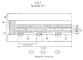
- FIG. 1is a cross-sectional view schematically showing a bottom emission organic EL device according to the related art, wherein a unit pixel region includes red (R), green (G) and blue (B) sub-pixels.
- the related art bottom emission organic EL deviceincludes a first substrate 10 and a second substrate 30 facing each other and sealed by a seal pattern 40 .
- the first substrate 10includes a transparent substrate 1 , thin film transistors T formed in each sub-pixel on the transparent substrate 1 , first electrodes 12 connected with the thin film transistors T, an organic EL layer 14 connected with the thin film transistors T and disposed corresponding to the first electrodes 12 on the thin film transistors T, and a second electrode 16 formed on the organic EL layer 14 .
- the organic EL layer 14includes emission materials emitting red (R), green (G) and blue colors.
- the first and second electrodes 12 and 16apply an electric field to the organic EL layer 14 .
- the second electrode 16is spaced away from the second substrate 30 by the seal pattern 40 .
- a moisture absorbent (not shown) for preventing moisture from leaking to an outsideis filled into an inner surface of the second substrate 30 and fixed by a semi-transparent tape (not shown).
- the first electrode 12serves as an anode and is selected from a group consisting of transparent conductive materials
- the second electrode 16serves as a cathode and is selected from a group consisting of metal materials having a low work function.
- the organic EL layer 14has a stack structure where a hole injection layer 14 a , a hole transporting layer 14 b , an emission layer 14 c , an electron transporting layer 14 d that are sequentially stacked starting from the hole injection layer 14 a contacting the first electrode 12 .
- the emission layer 14 chas a structure in which the emission materials emitting red (R), green (G) and blue colors are sequentially arranged corresponding to the respective sub-pixels.
- the related art organic EL devicehas a limitation in fine-patterning the red (R), green (G) and blue pixels with high reproduction under a large area.
- the organic EL material for the organic EL layer 14is vulnerable to solvent or moisture, it cannot be patterned by a wet etch. For this reason, the organic EL material cannot be patterned by photolithography, which is advantageous in forming fine patterns.
- Low molecular organic EL materialcan be patterned by a method including installing a fine-patterned shadow mask on a substrate and then independently forming R, G, B materials.
- this methodis limited in precisely fabricating the shadow mask to have fine patterns over a resolution of a predetermined level and employing the shadow mask in a high definition and large area due to the tension deviation of the shadow mask and the like.
- another pixel patterning method using a high molecular organic EL material inkjet injection headhas been researched, but it is difficult for forming a pinhole-free thin film less than 1000 ⁇ .
- the related art bottom emission structure organic EL devicesare fabricated by attaching the first substrate 10 provided with an array device and an organic EL diode to the second substrate 30 for separate encapsulation.
- a yield of the organic EL displayis determined by both of a yield of the array device and a yield of the organic EL diode, and therefore, an overall process yield is greatly limited to a latter process, namely, the process of forming the organic EL diode.
- the array deviceis formed excellently, if defects occur due to foreign matters or other factors in forming the organic EL layer employing a thin film of about 1000 ⁇ thick, the entire organic EL device is rendered defective. Consequently, a defective organic EL layer results in decreased production yield and increased material costs in manufacturing the non-defective array element associated with the defective organic EL layer.
- the bottom emission structuresince the bottom emission structure has high stability and high process freedom because of the encapsulation, but has a limitation in the aperture ratio, it is suitable to employ the bottom emission structure for high resolution products.
- the present inventionis directed to an organic EL device that substantially obviates one or more problems due to limitations and disadvantages of the related art.
- An object of the present inventionis to provide a dual panel type organic EL device that is capable of obtaining a high color purity by forming an organic EL layer in a stack structure including a charge generation layer, an electrode transporting layer, a hole transporting layer, and an emission layer including red (R), green (G) and blue (B) emission materials, so that the dual panel type organic EL device can exhibit full colors using a color conversion medium (CCM)/color filter or a color filter.
- CCMcolor conversion medium
- an organic EL deviceincluding: a first substrate and a second substrate spaced apart from each other by a predetermined interval and facing each other; an array element divided into sub-pixels and including thin film transistors formed in the sub-pixels; a color conversion portion disposed below the second substrate and including a red (R), green (G) and blue (B) conversion layer for converting white light into three primary colors of red (R), green (G) and blue (B); a first electrode disposed below the color conversion portion and including a transparent conductive material; an organic EL layer disposed below the first electrode in the sub-pixels and including a plurality of stack units each including a charge generation layer, an electrode transporting layer, a hole transporting layer and an emission layer; a second electrode patterned below the organic EL layer in the sub-pixels; and a conductive spacer electrically connecting the thin film transistors with the second electrode.
- the method of fabricating the organic EL deviceincludes a first substrate and a second substrate spaced apart from each other by a predetermined interval and facing each other; an array element divided into sub-pixels and including thin film transistors formed in the sub-pixels; color filters disposed below the second substrate; a first electrode disposed below the color filters and including a transparent conductive material; an organic EL layer disposed below the first electrode in the sub-pixels and including a plurality of stack units each including a charge generation layer (CGL), an electrode transporting layer (ETL), a hole transporting layer (HTL) and an emission layer (EMT); a second electrode patterned below the organic EL layer in the sub-pixels; and a conductive spacer electrically connecting the thin film transistors with the second electrode.
- CGLcharge generation layer
- ETLelectrode transporting layer
- HTLhole transporting layer
- EMTemission layer
- FIG. 1is a cross-sectional view schematically showing a bottom emission organic EL device according to the related art
- FIG. 2is a cross-sectional view schematically showing an organic EL device according to an exemplary embodiment of the present invention
- FIG. 3is a cross-sectional view schematically showing an organic EL device according to another exemplary embodiment of the present invention.
- FIG. 4is a cross-sectional view illustrating a an organic EL layer disposed on in the organic EL devices shown in FIGS. 2 and 3 .
- FIG. 2is a cross-sectional view schematically showing a dual panel type organic EL device that exhibits colors in a color conversion medium (CCM) according to an exemplary embodiment of the present invention.
- the dual panel type organic EL deviceis capable of overcoming the drawbacks of the related art bottom emission type organic EL device.
- the dual panel type organic EL deviceincludes a first substrate 110 and a second substrate 130 disposed facing each other and attached by a seal pattern 160 .
- the first substrate 110includes a transparent substrate 100 and an array element 112 formed on the transparent substrate 100 .
- the second substrate 130includes a transparent substrate 101 , and a color conversion portion 136 .
- the color conversion portion 136including red (R), green (G) and blue (B) color conversion layers 132 a , 132 b and 132 c sequentially arranged in a horizontal direction in the sub-pixel, and a black matrix (BM) layer 134 formed at boundaries between the R, G, B color conversion layers 132 a , 132 b and 132 c to prevent color interference between colors and light leakage.
- RGBred
- Ggreen
- Bblue
- BMblack matrix
- An overcoat layer 138is deposited beneath the color conversion portion 136 , and a first electrode 140 is deposited as a common electrode below the overcoat layer 138 .
- the first electrode 140may be made of a conductive material with light transmission capability.
- a trapezoidal electrode separator 142 of insulatoris disposed at boundaries of the sub-pixels below the first electrode 142 .
- An organic EL layer 500 and a second electrode 146are independently disposed between the adjacent electrode separators 142 and correspond to each sub-pixel.
- the color conversion portion 136may include R, G and B color filters. Since the electrode separator 142 serves to pattern the second electrode 146 in each sub-pixel, the electrode separator 142 preferably has a trapezoidal structure in which width is reduced from the second electrode 146 to the first electrode 140 .
- the seal pattern 160is formed along an edge between the first and second substrates 110 and 130 to attach them and to maintain a constant cell gap.
- the array element 112 on the first substrate 110includes a thin film transistor 112 a as a switching element, and an electrical connector 112 b connected with the thin film transistor 112 a .
- Conductive spacers 148 for electrically connecting the electrical connectors 112 b of the first substrate 110 with the second electrode 146 of the second substrate 130are formed in each sub-pixel.
- the thin film transistor 112 acorresponds to a drive transistor connected with the organic EL diode E.
- the electrical connector 112 bmay correspond to any of source and drain electrodes (not shown) of the thin film transistor 112 a , or may be made of a separate conductive material connected with the source and drain electrodes.
- the organic EL layer 500has a multi-layered structure depending on the arrangement of anode and cathode.
- the organic EL layer 500has the multi-layered structure such that a hole injection layer contacting the first electrode 140 , a hole transporting layer, an emission layer, an electron transporting layer, an electron injection layer are sequentially arranged.
- the conductive spacers 148 connecting the second electrode 146 with the thin film transistor 112 aare formed between the second electrodes 146 and the electrical connectors 112 b.
- the conductive spacers 148are used to electrically connect the two substrates as well as to maintain a cell gap between the two substrates 110 and 130 , and each have a column shape having a predetermined height.
- the conductive spacers 148are formed by coating a conductive film on an insulator column spacer to electrically connect the two substrates 110 and 130 and also serve as spacers.
- the conductive metal film coating the conductive spacer 148is flexible and made of one selected from the group of metal materials having a low resistivity.
- the conductive spacer 148may be formed during a process of forming an array device of the first substrate 110 .
- the above dual panel type organic EL deviceis a top emission type that emits light generated from the organic EL layer 500 toward the second substrate 130 .
- the first electrode 140should be selected from the group consisting of transparent conductive materials. If the first electrode 140 serves as an anode, it may be made of ITO. On the other hand, if the first electrode 140 serves as a cathode, it is preferably made of a semi-transparent metal material having a low work function.
- the semi-transparent metal materialmay be selected from the group consisting of aluminum (Al), an alloy of magnesium (Mg) and Al (hereinafter referred to as ‘Mg:Al’), Al:Li and Al:benzonate.
- the second electrode 146is an electrode positioned at a rear side of the light emission direction, it is preferably selected from the group consisting of opaque metal materials.
- the second electrode 146is made of ITO and the opaque metal material may be further provided so as to perform as a reflective plate.
- the dual panel type organic EL device exhibiting full colors using the color conversion medium (CCM)/color filterhas a disadvantage in that the light emitted from the organic EL layer 500 may be somewhat lost while passing through the color filter or the color conversion layers 132 a , 132 b and 132 c .
- the organic EL layer 500may be designed to have a multi-photon emission (MPE) structure to emit R, G and B colored lights, thereby enhancing color purity.
- MPEmulti-photon emission
- a-Siamorphous silicon
- the current ratios required to the R, G and B pixelsare greatly influenced by a color coordinate of each color. According to the exemplary embodiment, the current ratios required are adjusted at a constant value, thereby preventing one color from being first degenerated.
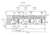
- FIG. 3is a cross-sectional view schematically illustrating an organic EL device according to another embodiment of the present invention.
- the organic EL deviceis different from the organic EL device shown in FIG. 2 in that color filters 400 a , 400 b and 400 c and organic EL layer 500 emitting white light are provided to exhibit full colors. Since other elements of the organic EL device shown in FIG. 3 other than the color filters 400 a , 400 b and 400 c and the organic EL layer 500 are the same as those of the organic EL device shown in FIG. 2 , like reference numerals are used to indicate like elements, and their descriptions are omitted. Moreover, in the organic EL device of FIG.
- the color conversion portion 136 except for the color conversion layers 132 a , 132 b and 132 c and the black matrix layer 134is not formed by employing the color filters 400 a , 400 b and 400 c and the organic EL layer 500 emitting white light.
- the organic EL layer 500includes the multi-photo emission structure to emit R, G and B colored lights, thereby enhancing the color purity.
- FIG. 4is a detailed sectional view of the organic EL layer shown in FIGS. 3 and 4 .
- the organic EL layer 500is formed between the trapezoidal electrode separators 142 and the second electrode 146 .
- the MPE structure of the organic EL layer 500includes a plurality of stack units including at least a first stack unit 510 , a second stack unit 520 and a third stack unit 530 .
- Each stack unitincludes charge generation layers 518 and 528 , electron transporting layers 512 , 522 and 532 , hole transporting layers 516 , 526 and 536 , and emission layers 514 , 524 and 534 .
- each of the emission layers 514 , 524 and 534includes R, G and B emission materials.
- the first stack unit 510includes the electron transporting layer 512 contacting the first electrode 140 , the emission layer 514 containing blue ‘B’ emission material, the hole transporting layer 516 and the charge generation layer 518 ; a second stack unit 520 includes the electron transporting layer 522 disposed below the charge generation layer 518 , the emission layer 524 containing green ‘G’ emission material, the second hole transporting layer 526 and the charge generation layer 528 ; and the third stack unit 530 includes the electron transporting layer 532 disposed below the charge generation layer 528 , the emission layer 534 containing red ‘R’ emission material and the hole transporting layer 536 .
- the hole transporting layer 536 of the third stack unit 530has a lower surface contacting the second electrode 146 .
- the third stack unit 530is not provided with a charge generation layer because the second electrode 146 may serve as the charge generation layer.
- the charge generation layersmay be made of V2O5, the electron transporting layers 512 , 522 and 532 may be made of Cs:BCP, and the hole transporting layers 516 , 526 and 536 may be made of ⁇ -NPD.
- the charge generation layers 518 and 528use the applied power to generate charges, i.e., electrons and holes and provide these charges to the adjacent electron transporting layers 512 , 522 and 532 and the hole transporting layers 516 , 526 and 536 .
- chargesare generated inside the charge generation layer 518 , and holes are supplied to the hole transporting layer 516 and then introduced into the emission layer 514 , whereas electrons is supplied to the electron transporting layer 522 and then introduced into the emission layer 524 .
- the above operationmay be equally applied to the charge generation layer 528 .
- the emission layers 514 , 524 and 534emit blue, green and red lights, independently.
- the MPE structure of the organic EL layerserves to emit red, green and blue lights independently, thereby obtaining high color purity.
- the organic EL layerincludes a stack structure in which the charge generation layer, the red, green and blue emission material layers are sequentially stacked, thereby enhancing the color purity.
- the current ratios required to the red, green and blue lightsare constantly maintained, thereby preventing one color from being degenerated and contributing to a long life span of the device.
Landscapes
- Physics & Mathematics (AREA)
- Optics & Photonics (AREA)
- Electroluminescent Light Sources (AREA)
Abstract
Description
Claims (6)
Applications Claiming Priority (3)
| Application Number | Priority Date | Filing Date | Title |
|---|---|---|---|
| KR10-2003-0099398 | 2003-12-29 | ||
| KR99398/2003 | 2003-12-29 | ||
| KR1020030099398AKR100670543B1 (en) | 2003-12-29 | 2003-12-29 | Organic electroluminescent device |
Publications (2)
| Publication Number | Publication Date |
|---|---|
| US20050140275A1 US20050140275A1 (en) | 2005-06-30 |
| US7696681B2true US7696681B2 (en) | 2010-04-13 |
Family
ID=34698701
Family Applications (1)
| Application Number | Title | Priority Date | Filing Date |
|---|---|---|---|
| US11/008,825Active2026-11-03US7696681B2 (en) | 2003-12-29 | 2004-12-23 | Stacked organic electroluminescent units for white light emission provided with RGB color conversion portions |
Country Status (3)
| Country | Link |
|---|---|
| US (1) | US7696681B2 (en) |
| KR (1) | KR100670543B1 (en) |
| CN (1) | CN1638570A (en) |
Cited By (12)
| Publication number | Priority date | Publication date | Assignee | Title |
|---|---|---|---|---|
| US20060260679A1 (en)* | 2005-05-20 | 2006-11-23 | Sukekazu Aratani | Organic light emitting display device |
| US20110248249A1 (en)* | 2008-10-28 | 2011-10-13 | Stephen Forrest | Stacked white oled having separate red, green and blue sub-elements |
| US20150034923A1 (en)* | 2013-07-31 | 2015-02-05 | Lg Display Co., Ltd. | White organic light emitting diode device |
| US20170084672A1 (en)* | 2004-12-16 | 2017-03-23 | Semiconductor Energy Laboratory Co., Ltd. | Light-Emitting Device and Electronic Device Using the Same |
| US20170125716A1 (en)* | 2015-05-04 | 2017-05-04 | Boe Technology Group Co., Ltd. | Organic light emitting diode and display device thereof |
| US9666822B2 (en) | 2013-12-17 | 2017-05-30 | The Regents Of The University Of Michigan | Extended OLED operational lifetime through phosphorescent dopant profile management |
| US20170331039A1 (en)* | 2016-05-12 | 2017-11-16 | Samsung Display Co., Ltd. | Organic light-emitting device |
| US10396296B2 (en)* | 2016-07-13 | 2019-08-27 | Samsung Display Co., Ltd. | Organic light-emitting device |
| WO2020050576A1 (en)* | 2018-09-03 | 2020-03-12 | Rohm And Haas Electronic Materials Korea Ltd. | Organic electroluminescent device |
| US20210013451A1 (en)* | 2014-10-09 | 2021-01-14 | Sony Corporation | Display unit, method of manufacturing display unit, and electronic apparatus |
| US11296152B2 (en)* | 2019-03-27 | 2022-04-05 | Boe Technology Group Co., Ltd. | Array substrate with color conversion luminescence layers, manufacturing method thereof, display panel, and display apparatus |
| US20220209118A1 (en)* | 2020-12-29 | 2022-06-30 | Lg Display Co., Ltd. | Luminescent compound, organic light emitting diode and organic light emitting device having the compound |
Families Citing this family (89)
| Publication number | Priority date | Publication date | Assignee | Title |
|---|---|---|---|---|
| US8487527B2 (en)* | 2005-05-04 | 2013-07-16 | Lg Display Co., Ltd. | Organic light emitting devices |
| US7777407B2 (en)* | 2005-05-04 | 2010-08-17 | Lg Display Co., Ltd. | Organic light emitting devices comprising a doped triazine electron transport layer |
| US7943244B2 (en)* | 2005-05-20 | 2011-05-17 | Lg Display Co., Ltd. | Display device with metal-organic mixed layer anodes |
| US7750561B2 (en)* | 2005-05-20 | 2010-07-06 | Lg Display Co., Ltd. | Stacked OLED structure |
| US7811679B2 (en)* | 2005-05-20 | 2010-10-12 | Lg Display Co., Ltd. | Display devices with light absorbing metal nanoparticle layers |
| US7795806B2 (en)* | 2005-05-20 | 2010-09-14 | Lg Display Co., Ltd. | Reduced reflectance display devices containing a thin-layer metal-organic mixed layer (MOML) |
| US7728517B2 (en)* | 2005-05-20 | 2010-06-01 | Lg Display Co., Ltd. | Intermediate electrodes for stacked OLEDs |
| CN100444425C (en)* | 2005-08-26 | 2008-12-17 | 中华映管股份有限公司 | Stacked organic electroluminescent device and method for manufacturing the same |
| US20070103056A1 (en)* | 2005-11-08 | 2007-05-10 | Eastman Kodak Company | OLED device having improved light output |
| US8698392B2 (en)* | 2006-02-07 | 2014-04-15 | Sumitomo Chemical Company, Limited | Organic electroluminescent element |
| JP2007242591A (en)* | 2006-03-08 | 2007-09-20 | Samsung Sdi Co Ltd | Organic electroluminescent display device and manufacturing method thereof |
| TWI307978B (en)* | 2006-04-28 | 2009-03-21 | Au Optronics Corp | Cascade organic electroluminescent device |
| US20080042146A1 (en)* | 2006-08-18 | 2008-02-21 | Cok Ronald S | Light-emitting device having improved ambient contrast |
| US7969085B2 (en)* | 2006-08-18 | 2011-06-28 | Global Oled Technology Llc | Color-change material layer |
| CN100428489C (en)* | 2006-09-15 | 2008-10-22 | 信利半导体有限公司 | Organic light emitting diode and its producing method |
| KR100796604B1 (en)* | 2006-12-15 | 2008-01-21 | 삼성에스디아이 주식회사 | Organic electroluminescent device and manufacturing method thereof |
| KR101407574B1 (en)* | 2007-01-12 | 2014-06-17 | 삼성디스플레이 주식회사 | White light emitting device |
| KR101499234B1 (en) | 2008-06-27 | 2015-03-05 | 삼성디스플레이 주식회사 | Organic light emitting device, method of manufacturing the same and shadow mask therefor |
| KR101511549B1 (en)* | 2008-07-25 | 2015-04-13 | 엘지디스플레이 주식회사 | Organic light emitting display |
| KR100965590B1 (en)* | 2008-07-25 | 2010-06-23 | 엘지디스플레이 주식회사 | Organic light emitting display |
| KR100958642B1 (en)* | 2008-09-04 | 2010-05-20 | 삼성모바일디스플레이주식회사 | Organic light emitting display and manufacturing method thereof |
| DE102009012346B4 (en)* | 2009-03-09 | 2024-02-15 | Merck Patent Gmbh | Organic electroluminescent device and method for producing the same |
| CN101872781B (en)* | 2009-04-27 | 2014-07-16 | 群创光电股份有限公司 | Image display system |
| US9899329B2 (en) | 2010-11-23 | 2018-02-20 | X-Celeprint Limited | Interconnection structures and methods for transfer-printed integrated circuit elements with improved interconnection alignment tolerance |
| US8889485B2 (en) | 2011-06-08 | 2014-11-18 | Semprius, Inc. | Methods for surface attachment of flipped active componenets |
| US8476624B1 (en)* | 2012-06-01 | 2013-07-02 | Au Optronics Corporation | Organic light emitting diode (OLED) device |
| CN102916138B (en)* | 2012-10-31 | 2016-01-06 | 昆山维信诺显示技术有限公司 | A kind of total colouring method and display unit |
| TWI527211B (en)* | 2012-12-28 | 2016-03-21 | Lg顯示器股份有限公司 | Organic light emitting display device and method of manufacturing the same |
| CN104916786B (en)* | 2014-03-13 | 2017-02-15 | 中国科学院苏州纳米技术与纳米仿生研究所 | Thin film packaging device |
| US9444015B2 (en) | 2014-06-18 | 2016-09-13 | X-Celeprint Limited | Micro assembled LED displays and lighting elements |
| WO2016030422A1 (en) | 2014-08-26 | 2016-03-03 | X-Celeprint Limited | Micro assembled hybrid displays and lighting elements |
| US9818725B2 (en) | 2015-06-01 | 2017-11-14 | X-Celeprint Limited | Inorganic-light-emitter display with integrated black matrix |
| US9799261B2 (en) | 2014-09-25 | 2017-10-24 | X-Celeprint Limited | Self-compensating circuit for faulty display pixels |
| US9799719B2 (en) | 2014-09-25 | 2017-10-24 | X-Celeprint Limited | Active-matrix touchscreen |
| US9991163B2 (en) | 2014-09-25 | 2018-06-05 | X-Celeprint Limited | Small-aperture-ratio display with electrical component |
| US9537069B1 (en) | 2014-09-25 | 2017-01-03 | X-Celeprint Limited | Inorganic light-emitting diode with encapsulating reflector |
| US9871345B2 (en)* | 2015-06-09 | 2018-01-16 | X-Celeprint Limited | Crystalline color-conversion device |
| US10133426B2 (en) | 2015-06-18 | 2018-11-20 | X-Celeprint Limited | Display with micro-LED front light |
| US11061276B2 (en) | 2015-06-18 | 2021-07-13 | X Display Company Technology Limited | Laser array display |
| US10255834B2 (en) | 2015-07-23 | 2019-04-09 | X-Celeprint Limited | Parallel redundant chiplet system for controlling display pixels |
| US9640108B2 (en) | 2015-08-25 | 2017-05-02 | X-Celeprint Limited | Bit-plane pulse width modulated digital display system |
| US10380930B2 (en) | 2015-08-24 | 2019-08-13 | X-Celeprint Limited | Heterogeneous light emitter display system |
| US10230048B2 (en) | 2015-09-29 | 2019-03-12 | X-Celeprint Limited | OLEDs for micro transfer printing |
| CN105374944A (en)* | 2015-11-25 | 2016-03-02 | 吕珩 | Organic light-emitting diode |
| US10066819B2 (en) | 2015-12-09 | 2018-09-04 | X-Celeprint Limited | Micro-light-emitting diode backlight system |
| US9930277B2 (en) | 2015-12-23 | 2018-03-27 | X-Celeprint Limited | Serial row-select matrix-addressed system |
| US9786646B2 (en) | 2015-12-23 | 2017-10-10 | X-Celeprint Limited | Matrix addressed device repair |
| US10091446B2 (en) | 2015-12-23 | 2018-10-02 | X-Celeprint Limited | Active-matrix displays with common pixel control |
| US9928771B2 (en) | 2015-12-24 | 2018-03-27 | X-Celeprint Limited | Distributed pulse width modulation control |
| US10361677B2 (en) | 2016-02-18 | 2019-07-23 | X-Celeprint Limited | Transverse bulk acoustic wave filter |
| US10200013B2 (en) | 2016-02-18 | 2019-02-05 | X-Celeprint Limited | Micro-transfer-printed acoustic wave filter device |
| US10109753B2 (en) | 2016-02-19 | 2018-10-23 | X-Celeprint Limited | Compound micro-transfer-printed optical filter device |
| TWI710061B (en) | 2016-02-25 | 2020-11-11 | 愛爾蘭商艾克斯展示公司技術有限公司 | Efficiently micro-transfer printing micro-scale devices onto large-format substrates |
| US10150325B2 (en) | 2016-02-29 | 2018-12-11 | X-Celeprint Limited | Hybrid banknote with electronic indicia |
| US10150326B2 (en) | 2016-02-29 | 2018-12-11 | X-Celeprint Limited | Hybrid document with variable state |
| US10193025B2 (en) | 2016-02-29 | 2019-01-29 | X-Celeprint Limited | Inorganic LED pixel structure |
| US10153256B2 (en) | 2016-03-03 | 2018-12-11 | X-Celeprint Limited | Micro-transfer printable electronic component |
| US10153257B2 (en) | 2016-03-03 | 2018-12-11 | X-Celeprint Limited | Micro-printed display |
| US10199546B2 (en) | 2016-04-05 | 2019-02-05 | X-Celeprint Limited | Color-filter device |
| US10008483B2 (en) | 2016-04-05 | 2018-06-26 | X-Celeprint Limited | Micro-transfer printed LED and color filter structure |
| US9997102B2 (en) | 2016-04-19 | 2018-06-12 | X-Celeprint Limited | Wirelessly powered display and system |
| US10198890B2 (en) | 2016-04-19 | 2019-02-05 | X-Celeprint Limited | Hybrid banknote with electronic indicia using near-field-communications |
| US10360846B2 (en) | 2016-05-10 | 2019-07-23 | X-Celeprint Limited | Distributed pulse-width modulation system with multi-bit digital storage and output device |
| US9997501B2 (en) | 2016-06-01 | 2018-06-12 | X-Celeprint Limited | Micro-transfer-printed light-emitting diode device |
| US10453826B2 (en) | 2016-06-03 | 2019-10-22 | X-Celeprint Limited | Voltage-balanced serial iLED pixel and display |
| US11137641B2 (en) | 2016-06-10 | 2021-10-05 | X Display Company Technology Limited | LED structure with polarized light emission |
| US9980341B2 (en) | 2016-09-22 | 2018-05-22 | X-Celeprint Limited | Multi-LED components |
| US10782002B2 (en) | 2016-10-28 | 2020-09-22 | X Display Company Technology Limited | LED optical components |
| US10347168B2 (en) | 2016-11-10 | 2019-07-09 | X-Celeprint Limited | Spatially dithered high-resolution |
| CN106449659B (en) | 2016-11-11 | 2019-06-07 | 京东方科技集团股份有限公司 | Array substrate and its manufacturing method, display |
| US10395966B2 (en) | 2016-11-15 | 2019-08-27 | X-Celeprint Limited | Micro-transfer-printable flip-chip structures and methods |
| US10600671B2 (en) | 2016-11-15 | 2020-03-24 | X-Celeprint Limited | Micro-transfer-printable flip-chip structures and methods |
| EP3542394B1 (en) | 2016-11-15 | 2025-09-24 | X Display Company Technology Limited | Micro-transfer-printable flip-chip structures and manufacturing methods thereof |
| US10438859B2 (en) | 2016-12-19 | 2019-10-08 | X-Celeprint Limited | Transfer printed device repair |
| US10832609B2 (en) | 2017-01-10 | 2020-11-10 | X Display Company Technology Limited | Digital-drive pulse-width-modulated output system |
| US10396137B2 (en) | 2017-03-10 | 2019-08-27 | X-Celeprint Limited | Testing transfer-print micro-devices on wafer |
| US11024608B2 (en) | 2017-03-28 | 2021-06-01 | X Display Company Technology Limited | Structures and methods for electrical connection of micro-devices and substrates |
| CN107425129B (en)* | 2017-07-26 | 2019-12-06 | 上海天马有机发光显示技术有限公司 | An organic light-emitting display panel, its color temperature adjustment method and display device |
| CN107910454A (en)* | 2017-11-03 | 2018-04-13 | 武汉华星光电半导体显示技术有限公司 | A kind of OLED display panel and its manufacture method |
| TWI673544B (en)* | 2018-05-09 | 2019-10-01 | 友達光電股份有限公司 | Display panel and electronic device comprising thereof |
| CN108877521A (en)* | 2018-06-28 | 2018-11-23 | 京东方科技集团股份有限公司 | information display and information display device |
| TWI681556B (en)* | 2018-09-11 | 2020-01-01 | 友達光電股份有限公司 | Light emitting diode display apparatus and manufacturing method thereof |
| KR102733723B1 (en)* | 2018-12-28 | 2024-11-22 | 엘지디스플레이 주식회사 | Organic light emitting diode and organic light emitting device having thereof |
| JP7138286B2 (en)* | 2018-12-28 | 2022-09-16 | 日亜化学工業株式会社 | Image display device and image display device manufacturing method |
| KR102733495B1 (en)* | 2018-12-28 | 2024-11-21 | 엘지디스플레이 주식회사 | Organic light emitting diode and orgnic light emitting device including the same |
| KR102727943B1 (en)* | 2018-12-28 | 2024-11-07 | 엘지디스플레이 주식회사 | Organic light emitting diode and organic light emitting device having thereof |
| CN110459586B (en)* | 2019-08-30 | 2021-10-15 | 云谷(固安)科技有限公司 | Array substrate and display panel |
| KR102326512B1 (en)* | 2020-01-14 | 2021-11-16 | 덕산네오룩스 주식회사 | Compound for organic electronic element, organic electronic element using the same, and an electronic device thereof |
| KR20230145091A (en)* | 2021-02-12 | 2023-10-17 | 가부시키가이샤 한도오따이 에네루기 켄큐쇼 | Display device, method of manufacturing display device, display module, and electronic device |
Citations (4)
| Publication number | Priority date | Publication date | Assignee | Title |
|---|---|---|---|---|
| US20010000005A1 (en) | 1994-12-13 | 2001-03-15 | Forrest Stephen R. | Transparent contacts for organic devices |
| CN1438828A (en) | 2002-02-15 | 2003-08-27 | 伊斯曼柯达公司 | Organic electroluminescent device of electroluminescent unit with lamina |
| US20030178936A1 (en)* | 2002-03-20 | 2003-09-25 | Lg.Philips Lcd Co., Ltd. | Organic electroluminescent device and method of fabricating the same |
| JP2003272860A (en) | 2002-03-26 | 2003-09-26 | Junji Kido | Organic electroluminescent device |
- 2003
- 2003-12-29KRKR1020030099398Apatent/KR100670543B1/ennot_activeExpired - Lifetime
- 2004
- 2004-12-23USUS11/008,825patent/US7696681B2/enactiveActive
- 2004-12-29CNCNA2004101035127Apatent/CN1638570A/enactivePending
Patent Citations (10)
| Publication number | Priority date | Publication date | Assignee | Title |
|---|---|---|---|---|
| US20010000005A1 (en) | 1994-12-13 | 2001-03-15 | Forrest Stephen R. | Transparent contacts for organic devices |
| CN1438828A (en) | 2002-02-15 | 2003-08-27 | 伊斯曼柯达公司 | Organic electroluminescent device of electroluminescent unit with lamina |
| US20030170491A1 (en)* | 2002-02-15 | 2003-09-11 | Eastman Kodak Company | Providing an organic electroluminescent device having stacked electroluminescent units |
| US20030178936A1 (en)* | 2002-03-20 | 2003-09-25 | Lg.Philips Lcd Co., Ltd. | Organic electroluminescent device and method of fabricating the same |
| KR20030075771A (en) | 2002-03-20 | 2003-09-26 | 엘지.필립스 엘시디 주식회사 | Organic Electroluminescent Device and Method for Fabricating the same |
| CN1446032A (en) | 2002-03-20 | 2003-10-01 | Lg.菲利浦Lcd株式会社 | Organic electroluminescent apparatus and manufacturing method thereof |
| JP2003272860A (en) | 2002-03-26 | 2003-09-26 | Junji Kido | Organic electroluminescent device |
| CN1447629A (en) | 2002-03-26 | 2003-10-08 | 城户淳二 | organic electroluminescent element |
| US20030189401A1 (en)* | 2002-03-26 | 2003-10-09 | International Manufacturing And Engineering Services Co., Ltd. | Organic electroluminescent device |
| US20070182317A1 (en) | 2002-03-26 | 2007-08-09 | Junji Kido And Imes Co., Ltd. | Organic electroluminescent device |
Cited By (23)
| Publication number | Priority date | Publication date | Assignee | Title |
|---|---|---|---|---|
| US10475856B2 (en)* | 2004-12-16 | 2019-11-12 | Semiconductor Energy Laboratory Co., Ltd. | Light-emitting device and electronic device using the same |
| US20170084672A1 (en)* | 2004-12-16 | 2017-03-23 | Semiconductor Energy Laboratory Co., Ltd. | Light-Emitting Device and Electronic Device Using the Same |
| US20060260679A1 (en)* | 2005-05-20 | 2006-11-23 | Sukekazu Aratani | Organic light emitting display device |
| US8158969B2 (en)* | 2005-05-20 | 2012-04-17 | Hitachi Displays, Ltd. | Organic light emitting display device |
| US9065067B2 (en) | 2008-10-28 | 2015-06-23 | The Regents Of The University Of Michigan | Stacked white OLED having separate red, green and blue sub-elements |
| US20110248249A1 (en)* | 2008-10-28 | 2011-10-13 | Stephen Forrest | Stacked white oled having separate red, green and blue sub-elements |
| US20160276614A1 (en)* | 2008-10-28 | 2016-09-22 | The Regents Of The University Of Michigan | Stacked White OLED Having Separate Red, Green and Blue Sub-Elements |
| US8766291B2 (en)* | 2008-10-28 | 2014-07-01 | The Regents Of The University Of Michigan | Stacked white OLED having separate red, green and blue sub-elements |
| US10014485B2 (en)* | 2008-10-28 | 2018-07-03 | The Regents Of The University Of Michigan | Stacked white OLED having separate red, green and blue sub-elements |
| US9281487B2 (en)* | 2013-07-31 | 2016-03-08 | Lg Display Co., Ltd. | White organic light emitting diode device |
| US20150034923A1 (en)* | 2013-07-31 | 2015-02-05 | Lg Display Co., Ltd. | White organic light emitting diode device |
| US9666822B2 (en) | 2013-12-17 | 2017-05-30 | The Regents Of The University Of Michigan | Extended OLED operational lifetime through phosphorescent dopant profile management |
| US11563198B2 (en)* | 2014-10-09 | 2023-01-24 | Sony Corporation | Display unit with organic layer disposed on metal layer and insulation layer |
| US20210013451A1 (en)* | 2014-10-09 | 2021-01-14 | Sony Corporation | Display unit, method of manufacturing display unit, and electronic apparatus |
| US20170125716A1 (en)* | 2015-05-04 | 2017-05-04 | Boe Technology Group Co., Ltd. | Organic light emitting diode and display device thereof |
| US9899621B2 (en)* | 2015-05-04 | 2018-02-20 | Boe Technology Group Co., Ltd. | Organic light emitting diode and display device thereof |
| US10811614B2 (en)* | 2016-05-12 | 2020-10-20 | Samsung Display Co., Ltd. | Organic light-emitting device |
| US20170331039A1 (en)* | 2016-05-12 | 2017-11-16 | Samsung Display Co., Ltd. | Organic light-emitting device |
| US10396296B2 (en)* | 2016-07-13 | 2019-08-27 | Samsung Display Co., Ltd. | Organic light-emitting device |
| WO2020050576A1 (en)* | 2018-09-03 | 2020-03-12 | Rohm And Haas Electronic Materials Korea Ltd. | Organic electroluminescent device |
| US11296152B2 (en)* | 2019-03-27 | 2022-04-05 | Boe Technology Group Co., Ltd. | Array substrate with color conversion luminescence layers, manufacturing method thereof, display panel, and display apparatus |
| US20220209118A1 (en)* | 2020-12-29 | 2022-06-30 | Lg Display Co., Ltd. | Luminescent compound, organic light emitting diode and organic light emitting device having the compound |
| US12268083B2 (en)* | 2020-12-29 | 2025-04-01 | Lg Display Co., Ltd. | Luminescent compound, organic light emitting diode and organic light emitting device having the compound |
Also Published As
| Publication number | Publication date |
|---|---|
| KR20050068234A (en) | 2005-07-05 |
| CN1638570A (en) | 2005-07-13 |
| KR100670543B1 (en) | 2007-01-16 |
| US20050140275A1 (en) | 2005-06-30 |
Similar Documents
| Publication | Publication Date | Title |
|---|---|---|
| US7696681B2 (en) | Stacked organic electroluminescent units for white light emission provided with RGB color conversion portions | |
| US7279715B2 (en) | Organic electroluminescent display device | |
| US7518147B2 (en) | Organic electro luminescence device and fabrication method thereof | |
| US7258589B2 (en) | Organic electroluminescent device and method of fabricating the same | |
| US6831298B2 (en) | Dual panel-type organic electroluminescent display device | |
| US8025544B2 (en) | Method for manufacturing dual panel-type organic electroluminescent display device | |
| US6930331B2 (en) | Thin film transistor for use in active matrix type organic light emitting diode device | |
| KR20000047779A (en) | Color electro luminescent display | |
| US6870197B2 (en) | Dual panel type organic electroluminescent display device and method of fabricating the same | |
| US7745992B2 (en) | Organic electroluminescence device having electrode separator and light shielding pattern | |
| US7759860B2 (en) | Dual panel-type organic electroluminescent display device and method of fabricating the same | |
| US7547239B2 (en) | Organic electroluminescence device and fabrication method thereof | |
| US7459848B2 (en) | Organic electroluminescence device and fabrication method thereof | |
| KR100588868B1 (en) | Organic electroluminescent device and manufacturing method thereof | |
| KR101222985B1 (en) | Organic Emtting Device | |
| KR100593101B1 (en) | Organic electroluminescent device | |
| KR20050104100A (en) | Organic electro luminescence device and fabrication method thereof | |
| KR20040061988A (en) | Hybrid Structure Organic Electroluminescent Device and method for fabricating the same |
Legal Events
| Date | Code | Title | Description |
|---|---|---|---|
| AS | Assignment | Owner name:LG.PHILIPS LCD CO., LTD., KOREA, REPUBLIC OF Free format text:ASSIGNMENT OF ASSIGNORS INTEREST;ASSIGNOR:PARK, JAE YONG;REEL/FRAME:016111/0495 Effective date:20041221 Owner name:LG.PHILIPS LCD CO., LTD.,KOREA, REPUBLIC OF Free format text:ASSIGNMENT OF ASSIGNORS INTEREST;ASSIGNOR:PARK, JAE YONG;REEL/FRAME:016111/0495 Effective date:20041221 | |
| AS | Assignment | Owner name:LG DISPLAY CO., LTD., KOREA, REPUBLIC OF Free format text:CHANGE OF NAME;ASSIGNOR:LG.PHILIPS LCD CO., LTD.;REEL/FRAME:021147/0009 Effective date:20080319 Owner name:LG DISPLAY CO., LTD.,KOREA, REPUBLIC OF Free format text:CHANGE OF NAME;ASSIGNOR:LG.PHILIPS LCD CO., LTD.;REEL/FRAME:021147/0009 Effective date:20080319 | |
| FEPP | Fee payment procedure | Free format text:PAYOR NUMBER ASSIGNED (ORIGINAL EVENT CODE: ASPN); ENTITY STATUS OF PATENT OWNER: LARGE ENTITY | |
| STCF | Information on status: patent grant | Free format text:PATENTED CASE | |
| FPAY | Fee payment | Year of fee payment:4 | |
| MAFP | Maintenance fee payment | Free format text:PAYMENT OF MAINTENANCE FEE, 8TH YEAR, LARGE ENTITY (ORIGINAL EVENT CODE: M1552) Year of fee payment:8 | |
| MAFP | Maintenance fee payment | Free format text:PAYMENT OF MAINTENANCE FEE, 12TH YEAR, LARGE ENTITY (ORIGINAL EVENT CODE: M1553); ENTITY STATUS OF PATENT OWNER: LARGE ENTITY Year of fee payment:12 |