US7696056B2 - Methods of forming capacitors - Google Patents
Methods of forming capacitorsDownload PDFInfo
- Publication number
- US7696056B2 US7696056B2US12/114,129US11412908AUS7696056B2US 7696056 B2US7696056 B2US 7696056B2US 11412908 AUS11412908 AUS 11412908AUS 7696056 B2US7696056 B2US 7696056B2
- Authority
- US
- United States
- Prior art keywords
- opening
- bridging
- etching
- base material
- forming
- Prior art date
- Legal status (The legal status is an assumption and is not a legal conclusion. Google has not performed a legal analysis and makes no representation as to the accuracy of the status listed.)
- Active
Links
- 239000003990capacitorSubstances0.000titleclaimsabstractdescription113
- 238000000034methodMethods0.000titleclaimsabstractdescription46
- 239000000463materialSubstances0.000claimsabstractdescription283
- 238000005530etchingMethods0.000claimsabstractdescription79
- 239000000758substrateSubstances0.000claimsabstractdescription51
- 239000011800void materialSubstances0.000claimsabstractdescription14
- VYPSYNLAJGMNEJ-UHFFFAOYSA-NSilicium dioxideChemical compoundO=[Si]=OVYPSYNLAJGMNEJ-UHFFFAOYSA-N0.000claimsdescription29
- 238000000151depositionMethods0.000claimsdescription28
- 230000008021depositionEffects0.000claimsdescription17
- 235000012239silicon dioxideNutrition0.000claimsdescription15
- 239000000377silicon dioxideSubstances0.000claimsdescription14
- XUIMIQQOPSSXEZ-UHFFFAOYSA-NSiliconChemical compound[Si]XUIMIQQOPSSXEZ-UHFFFAOYSA-N0.000claimsdescription11
- 229910052710siliconInorganic materials0.000claimsdescription11
- 239000010703siliconSubstances0.000claimsdescription11
- 229910052799carbonInorganic materials0.000claimsdescription5
- 230000008018meltingEffects0.000claimsdescription5
- 238000002844meltingMethods0.000claimsdescription5
- 229920000642polymerPolymers0.000claimsdescription4
- 239000010410layerSubstances0.000description23
- 239000000203mixtureSubstances0.000description10
- 229910021420polycrystalline siliconInorganic materials0.000description6
- 229920005591polysiliconPolymers0.000description6
- 238000003860storageMethods0.000description6
- 229910052581Si3N4Inorganic materials0.000description5
- 238000010276constructionMethods0.000description5
- HQVNEWCFYHHQES-UHFFFAOYSA-Nsilicon nitrideChemical compoundN12[Si]34N5[Si]62N3[Si]51N64HQVNEWCFYHHQES-UHFFFAOYSA-N0.000description5
- ZOXJGFHDIHLPTG-UHFFFAOYSA-NBoronChemical compound[B]ZOXJGFHDIHLPTG-UHFFFAOYSA-N0.000description4
- 229910052796boronInorganic materials0.000description4
- 239000005380borophosphosilicate glassSubstances0.000description4
- 239000005360phosphosilicate glassSubstances0.000description4
- OAICVXFJPJFONN-UHFFFAOYSA-NPhosphorusChemical compound[P]OAICVXFJPJFONN-UHFFFAOYSA-N0.000description3
- 239000012634fragmentSubstances0.000description3
- 239000007788liquidSubstances0.000description3
- 238000004519manufacturing processMethods0.000description3
- 230000000873masking effectEffects0.000description3
- 229910052698phosphorusInorganic materials0.000description3
- 239000011574phosphorusSubstances0.000description3
- 239000002243precursorSubstances0.000description3
- 239000004065semiconductorSubstances0.000description3
- BOTDANWDWHJENH-UHFFFAOYSA-NTetraethyl orthosilicateChemical groupCCO[Si](OCC)(OCC)OCCBOTDANWDWHJENH-UHFFFAOYSA-N0.000description2
- 238000000429assemblyMethods0.000description2
- 230000000712assemblyEffects0.000description2
- 239000005388borosilicate glassSubstances0.000description2
- 229910021332silicideInorganic materials0.000description2
- FVBUAEGBCNSCDD-UHFFFAOYSA-Nsilicide(4-)Chemical compound[Si-4]FVBUAEGBCNSCDD-UHFFFAOYSA-N0.000description2
- 125000006850spacer groupChemical group0.000description2
- 239000000126substanceSubstances0.000description2
- XLYOFNOQVPJJNP-UHFFFAOYSA-NwaterSubstancesOXLYOFNOQVPJJNP-UHFFFAOYSA-N0.000description2
- OKTJSMMVPCPJKN-UHFFFAOYSA-NCarbonChemical compound[C]OKTJSMMVPCPJKN-UHFFFAOYSA-N0.000description1
- XPDWGBQVDMORPB-UHFFFAOYSA-NFluoroformChemical compoundFC(F)FXPDWGBQVDMORPB-UHFFFAOYSA-N0.000description1
- 229910003915SiCl2H2Inorganic materials0.000description1
- 229910003910SiCl4Inorganic materials0.000description1
- 229910004014SiF4Inorganic materials0.000description1
- BLRPTPMANUNPDV-UHFFFAOYSA-NSilaneChemical compound[SiH4]BLRPTPMANUNPDV-UHFFFAOYSA-N0.000description1
- NRTOMJZYCJJWKI-UHFFFAOYSA-NTitanium nitrideChemical compound[Ti]#NNRTOMJZYCJJWKI-UHFFFAOYSA-N0.000description1
- 239000006117anti-reflective coatingSubstances0.000description1
- 238000000231atomic layer depositionMethods0.000description1
- QVGXLLKOCUKJST-UHFFFAOYSA-Natomic oxygenChemical compound[O]QVGXLLKOCUKJST-UHFFFAOYSA-N0.000description1
- 229910052454barium strontium titanateInorganic materials0.000description1
- 230000015572biosynthetic processEffects0.000description1
- 238000005234chemical depositionMethods0.000description1
- 239000002131composite materialSubstances0.000description1
- 239000004020conductorSubstances0.000description1
- 238000000354decomposition reactionMethods0.000description1
- 230000003247decreasing effectEffects0.000description1
- 239000003989dielectric materialSubstances0.000description1
- RWRIWBAIICGTTQ-UHFFFAOYSA-NdifluoromethaneChemical compoundFCFRWRIWBAIICGTTQ-UHFFFAOYSA-N0.000description1
- NBVXSUQYWXRMNV-UHFFFAOYSA-NfluoromethaneChemical compoundFCNBVXSUQYWXRMNV-UHFFFAOYSA-N0.000description1
- 230000006870functionEffects0.000description1
- 239000007789gasSubstances0.000description1
- BHEPBYXIRTUNPN-UHFFFAOYSA-Nhydridophosphorus(.) (triplet)Chemical compound[PH]BHEPBYXIRTUNPN-UHFFFAOYSA-N0.000description1
- 239000012212insulatorSubstances0.000description1
- VNWKTOKETHGBQD-UHFFFAOYSA-NmethaneChemical compoundCVNWKTOKETHGBQD-UHFFFAOYSA-N0.000description1
- 229910052760oxygenInorganic materials0.000description1
- 239000001301oxygenSubstances0.000description1
- 238000000059patterningMethods0.000description1
- 230000002093peripheral effectEffects0.000description1
- 238000005498polishingMethods0.000description1
- 238000004080punchingMethods0.000description1
- FDNAPBUWERUEDA-UHFFFAOYSA-Nsilicon tetrachlorideChemical compoundCl[Si](Cl)(Cl)ClFDNAPBUWERUEDA-UHFFFAOYSA-N0.000description1
- ABTOQLMXBSRXSM-UHFFFAOYSA-Nsilicon tetrafluorideChemical compoundF[Si](F)(F)FABTOQLMXBSRXSM-UHFFFAOYSA-N0.000description1
- PBCFLUZVCVVTBY-UHFFFAOYSA-Ntantalum pentoxideInorganic materialsO=[Ta](=O)O[Ta](=O)=OPBCFLUZVCVVTBY-UHFFFAOYSA-N0.000description1
- TXEYQDLBPFQVAA-UHFFFAOYSA-NtetrafluoromethaneChemical compoundFC(F)(F)FTXEYQDLBPFQVAA-UHFFFAOYSA-N0.000description1
- 238000001039wet etchingMethods0.000description1
Images


Classifications
- H—ELECTRICITY
- H10—SEMICONDUCTOR DEVICES; ELECTRIC SOLID-STATE DEVICES NOT OTHERWISE PROVIDED FOR
- H10D—INORGANIC ELECTRIC SEMICONDUCTOR DEVICES
- H10D1/00—Resistors, capacitors or inductors
- H10D1/01—Manufacture or treatment
- H10D1/041—Manufacture or treatment of capacitors having no potential barriers
- H10D1/042—Manufacture or treatment of capacitors having no potential barriers using deposition processes to form electrode extensions
- H—ELECTRICITY
- H10—SEMICONDUCTOR DEVICES; ELECTRIC SOLID-STATE DEVICES NOT OTHERWISE PROVIDED FOR
- H10B—ELECTRONIC MEMORY DEVICES
- H10B12/00—Dynamic random access memory [DRAM] devices
- H10B12/01—Manufacture or treatment
- H10B12/02—Manufacture or treatment for one transistor one-capacitor [1T-1C] memory cells
- H10B12/03—Making the capacitor or connections thereto
- H10B12/033—Making the capacitor or connections thereto the capacitor extending over the transistor
- H—ELECTRICITY
- H10—SEMICONDUCTOR DEVICES; ELECTRIC SOLID-STATE DEVICES NOT OTHERWISE PROVIDED FOR
- H10B—ELECTRONIC MEMORY DEVICES
- H10B12/00—Dynamic random access memory [DRAM] devices
- H10B12/01—Manufacture or treatment
- H10B12/09—Manufacture or treatment with simultaneous manufacture of the peripheral circuit region and memory cells
- H—ELECTRICITY
- H10—SEMICONDUCTOR DEVICES; ELECTRIC SOLID-STATE DEVICES NOT OTHERWISE PROVIDED FOR
- H10D—INORGANIC ELECTRIC SEMICONDUCTOR DEVICES
- H10D1/00—Resistors, capacitors or inductors
- H10D1/60—Capacitors
- H10D1/68—Capacitors having no potential barriers
- H10D1/692—Electrodes
- H10D1/711—Electrodes having non-planar surfaces, e.g. formed by texturisation
- H10D1/716—Electrodes having non-planar surfaces, e.g. formed by texturisation having vertical extensions
- Y—GENERAL TAGGING OF NEW TECHNOLOGICAL DEVELOPMENTS; GENERAL TAGGING OF CROSS-SECTIONAL TECHNOLOGIES SPANNING OVER SEVERAL SECTIONS OF THE IPC; TECHNICAL SUBJECTS COVERED BY FORMER USPC CROSS-REFERENCE ART COLLECTIONS [XRACs] AND DIGESTS
- Y10—TECHNICAL SUBJECTS COVERED BY FORMER USPC
- Y10T—TECHNICAL SUBJECTS COVERED BY FORMER US CLASSIFICATION
- Y10T29/00—Metal working
- Y10T29/43—Electric condenser making
Definitions
- Embodiments disclosed hereinpertain to methods of forming capacitors.
- Capacitorsare one type of component commonly used in the fabrication of integrated circuits, for example in DRAM circuitry.
- a capacitoris comprised of two conductive electrodes separated by a non-conducting dielectric region.
- the increase in density of integrated circuitryhas typically resulted in greater reduction in the horizontal dimension of capacitors as compared to the vertical dimension. In many instances, the vertical dimension of capacitors has increased.
- One manner of fabricating capacitorsis to initially form an insulative material within which a capacitor storage node electrode is formed.
- an array of capacitor electrode openings for individual capacitorsmay be fabricated in such insulative capacitor electrode-forming material, with an example insulative electrode-forming material being silicon dioxide doped with one or both of phosphorus and boron.
- the capacitor electrode openingsmay be formed by etching. It can be difficult to etch the capacitor electrode openings within the insulative material, particularly where the openings have high aspect ratio.
- One manner of reducing such difficultyis to split the deposition and etch of such openings into two or more combinations of deposition and etch steps.
- the material within which the capacitor electrode openings are to be formedcan be deposited to an initial deposition thickness which is one half or less of the desired ultimate deposition thickness. Shallower capacitor electrode openings can then be etched to the underlying node location. Such openings are subsequently completely filled/plugged, and another material within which capacitor electrode openings will be formed is deposited over the material in which the first openings were formed and filled. Individual capacitor electrode openings are then formed through the overlying layer to the plugging material. Such can be repeated if desired. Regardless, the plugging material is at some point etched from the capacitor electrode openings to enable contact to be made to a node location on the substrate.
- One common plugging material used in such instancesis polysilicon.
- a native oxidecan form on the outermost surfaces thereof that can be difficult to remove. Such oxide can be removed by etching prior to etching the polysilicon within the openings from the substrate.
- the native oxide etchis usually conducted using an HF wet etching solution.
- the material within which the capacitor electrode openings are usually formedis a doped silicon dioxide, such as borophosphosilicate glass or phosphosilicate glass.
- the HFwill etch such material, thereby undesirably widening the capacitor electrode openings above the plugging material while removing the native oxide received thereover. Further and regardless, it can be difficult to remove the polysilicon plugging material from the openings.
- Example techniques in accordance with the aboveare described in U.S. Pat. Nos. 6,365,453 and 6,204,143.
- Fabrication of capacitors in integrated circuitry such as memory circuitrymay form an array of capacitors within a capacitor array area. Control or other circuitry area is often displaced from the capacitor array area, with the substrate including an intervening area between the capacitor array area and the control or other circuitry area. In some instances, a trench is formed in the intervening area between the capacitor array area and the other circuitry area. Such trench can be formed commensurate with the fabrication of the openings within the capacitor array area within which the isolated capacitor electrodes will be received.
- FIG. 1is a diagrammatic cross section of a substrate fragment in process in accordance with an aspect of the invention.
- FIG. 2is a diagrammatic top plan view of a larger scale portion of the FIG. 1 substrate.
- FIG. 3is a view of the FIG. 1 substrate at a processing step subsequent to that shown by FIG. 1 , and taken through line 3 - 3 in FIG. 4 .
- FIG. 4is a diagrammatic top plan view of the FIG. 3 substrate fragment.
- FIG. 5is a view of the FIG. 3 substrate at a processing step subsequent to that shown by FIG. 3 .
- FIG. 6is a view of the FIG. 5 substrate at a processing step subsequent to that shown by FIG. 5 .
- FIG. 7is a view of the FIG. 6 substrate at a processing step subsequent to that shown by FIG. 6 .
- FIG. 8is a view of the FIG. 7 substrate at a processing step subsequent to that shown by FIG. 7 .
- FIG. 9is a view of the FIG. 8 substrate at a processing step subsequent to that shown by FIG. 8 .
- FIG. 10is a view of the FIG. 9 substrate at a processing step subsequent to that shown by FIG. 9 .
- FIG. 11is a view of the FIG. 10 substrate at a processing step subsequent to that shown by FIG. 10 .
- FIG. 12is a view of the FIG. 11 substrate at a processing step subsequent to that shown by FIG. 11 , and taken through line 12 - 12 in FIG. 13 .
- FIG. 13is a diagrammatic top plan view of the FIG. 12 substrate fragment.
- FIG. 14is a view of the FIG. 12 substrate at a processing step subsequent to that shown by FIG. 12 .
- FIG. 15is a view of the FIG. 14 substrate at a processing step subsequent to that shown by FIG. 14 .
- FIG. 16is a diagrammatic representation of DRAM circuitry.
- a substratefor example a semiconductor substrate
- a substrateis indicated generally with reference numeral 10 .
- semiconductor substrateor “semiconductive substrate” is defined to mean any construction comprising semiconductive material, including, but not limited to, bulk semiconductive materials such as a semiconductive wafer (either alone or in assemblies comprising other materials thereon), and semiconductive material layers (either alone or in assemblies comprising other materials).
- substraterefers to any supporting structure, including, but not limited to, the semiconductive substrates described above. Accordingly, and by way of example only, FIG. 1 might comprise a bulk semiconductor material (not shown), for example bulk monocrystalline, and/or comprise semiconductor-on-insulator layers.
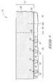
- Substrate 10can be considered as comprising a capacitor array area 25 , a circuitry area 75 other than capacitor array area 25 , and an intervening area 50 between capacitor array area 25 and circuitry area 75 .
- intervening area 50completely surrounds and encircles capacitor array area 25 ( FIG. 2 )
- circuitry area 75comprises a peripheral circuitry area to that of capacitor array area 25 .
- Alternate constructionsare contemplated, of course, for example whereby neither intervening area 50 nor circuitry area 75 completely or partially encircles a capacitor array area 25 .
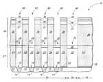
- FIG. 1depicts an insulative material 12 having electrically conductive storage node pillars 14 formed therethrough.
- Materials 12 and 14may be fabricated over some suitable underlying material, for example bulk monocrystalline and/or underlying circuitry.
- Example insulative materials 12include doped and undoped silicon dioxides, for example silicon dioxide deposited by the decomposition of tetraethylorthosilicate (TEOS) and/or borophosphosilicate glass (BPSG) and/or silicon nitride.
- TEOStetraethylorthosilicate
- BPSGborophosphosilicate glass
- silicon nitridesilicon nitride.
- doped silicon dioxideor “silicon dioxide doped” requires at least 0.5 atomic percent concentration of one or a combination of boron or phosphorus in silicon dioxide.
- an undoped silicon dioxiderequires less than 0.5 atomic percent of any of boron and phosphorous.
- material 12might comprise anisotropically etched insulative sidewall spacers, for example formed about transistor gate lines (not shown).
- An example material 14is conductively doped polysilicon. Conductive material 14 can be considered as comprising or defining a plurality of capacitor storage node locations 15 , 16 , 17 and 18 on substrate 10 . Storage node locations 15 , 16 , 17 and 18 are examples only, and regardless, may be conductive at this point in the process, or made conductive subsequently.
- a material 22has been formed over material 12 and capacitor storage node locations 15 , 16 , 17 and 18 .
- Examples for material 22comprise silicon nitride and/or undoped silicon dioxide deposited to an example thickness range of from about 100 Angstroms to about 2,000 Angstroms. Material 22 might be included to provide an etch stop, or other function.
- Some material 24is received over capacitor array area 25 and circuitry area 75 , and also in the depicted embodiment over intervening area 50 .
- Suchmight be homogeneous or comprise multiple different compositions and/or layers.
- An example materialis doped silicon dioxide, for example comprising at least one of phosphorus and boron, such as BPSG, borosilicate glass (BSG), and/or phosphosilicate glass (PSG).
- An example thickness range for material 24is from 5,000 Angstroms to 10 microns, with 2 microns being a specific example. Thinner and greater thicknesses are, of course, contemplated.
- layers 22 and 24comprise example base material 27 received over node locations 15 , 16 , 17 and 18 .
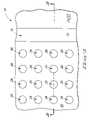
- a plurality of openings 28has been etched into base material 27 over individual node locations 15 , 16 , 17 and 18 . Further, a trench 30 has been formed in intervening area 50 within base material 27 . In one embodiment, trench 30 completely surrounds capacitor area 25 , area 25 .
- An example technique for forming capacitor electrode openings 28 and trench 30comprises photolithographic patterning and selective anisotropic dry etch to produce the example FIGS. 3 and 4 constructions.
- An example minimum width of trench opening 30is from about 200 Angstroms to about 5,000 Angstroms, while an example minimum width for capacitor electrode openings 28 is also from about 200 Angstroms to about 5,000 Angstroms.
- Trench 30may or may not be formed at this point in the process, or at all.
- the processing depicted by FIGS. 1-4depicts but one example method of providing a material (i.e. material 27 ) having an opening therein (i.e. any of openings 28 ) over a node location (i.e. any of locations 15 , 16 , 17 and 18 ) on a substrate.
- the opening(s)may or may not extend completely to the node locations at this point in the process.
- the processing depicted by FIGS. 3 and 4can occur in a suitable processing tool which for convenience in description can be considered as a “first processing tool”.
- the first processing toolmay be a plasma etcher.
- a LAMTM ExelanTM oxide etch toolis an example such tool.
- bridging material 32has been formed across base material openings 28 , with such openings 28 comprising voids 33 therebeneath.
- suchoccurs by depositing bridging material 32 over base material 27 and across base material openings 28 , and in one embodiment to partially within base material openings 28 as shown.
- suchoccurs in the very same first processing tool within which the etching to produce openings 28 in FIGS. 3 and 4 occurred, and in one embodiment before removing substrate 10 from such processing tool after such etching to produce openings 28 .
- example bridging materialsinclude silicon dioxide-comprising material; polymers comprising C, H, and F; and combinations of these and other materials.
- any silicon dioxide-comprising materialmay also include at least one of H, Cl, and F, for example provided in molar concentrations of from 10 to 20 percent of total atomic amount of silicon, oxygen and the at least one of H, Cl, and F. Regardless, these and/or other materials can be deposited by any existing or yet-to-be developed techniques.
- Example silicon-containing precursors for chemical or atomic layer depositioninclude SiH 4 , SiCl 4 , SiCl 2 H 2 , and SiF 4 .
- Example carbon-containing precursorsinclude CH 4 , CF 4 , CH 2 F 2 , CHF 3 , CH 3 F, C 4 F 6 , C 4 F 8 , C 2 F 4 , and C 6 F 6 .
- Example conditions during deposition within a plasma etcher or a plasma deposition toolinclude a chuck temperature of from 10° C. to 40° C., pressure from 10 mTorr to 200 mTorr, total power of from 500 watts to 2,000 watts and frequencies at one or a combination of 2 MHz and 27 MHz.
- quantity of the atomic components of the composition of bridging material 32can be controlled by quantity of precursor gases depending on the ultimate desired composition of bridging material 32 .
- Composition of material 32regardless, can be selected, controlled, and/or balanced in allowing greater or lesser resistance to subsequent processing steps (i.e. resistance to melting) and/or ease of subsequent removal of material 32 from openings 28 , as is described below.
- bridging material 32might be homogenous or non-homogenous.
- bridging material 32has been removed from being received over base material 27 and to leave bridging material 32 within and bridging across base material openings 28 .
- An example manner for doing soincludes chemical mechanical polishing. Alternately, removing of the bridging material might occur by an etching technique. For example in one embodiment, such could be etched by a timed etch within the first processing tool within which openings 28 were formed and bridging material 32 was formed.
- FIGS. 5 and 6depict, by way of examples only, methods of forming bridging material across base material openings which comprise a respective void beneath the bridging material.
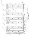
- covering material 34has been formed over base material 27 and bridging material 32 received within openings 28 . Such might be homogenous or non-homogenous, and regardless may comprise multiple layers.
- FIG. 7depicts covering material 34 as comprising four layers 36 , 37 , 38 , and 39 . Any of such materials may be the same or different in composition as one or more components of base material 27 .
- An example material 36is doped silicon dioxide
- an example material 37comprises silicon nitride
- example materials for layers 38 and 39include one or more different organic and/or inorganic antireflective coating layers. Regardless and in one embodiment, deposition of all of covering material 34 will comprise some highest deposition temperature in degrees C. at which any of such covering material 34 is deposited.
- bridging material 32is fabricated of a composition which will have a melting temperature in degrees C. which is at least 10% higher than said highest deposition temperature of any of covering material 34 .
- layer 37is the component of covering material 34 which has a highest deposition temperature of, for example, 350° C.
- bridging material 32 in such embodimentis fabricated to have a melting temperature of 385° C. or higher.
- openings 40have been etched through covering material 34 to bridging material 32 received across base material openings 28 .
- First capacitor electrodeswill ultimately be formed therein as is described below.
- a trench 42corresponding in general outline to trench 30 , is also shown as having been etched through covering material 34 to bridging material 32 received within trench 30 .
- Openings 40 and trench 42are shown as being the same size, shape, and exactly aligned with the respective openings 28 and trench 30 over which such lie. However, such may be of different such size and shape, and regardless may not exactly align over the underlying openings and trench.
- bridging material 32(not shown) has been etched through covering material openings 40 and 42 .
- such etching through bridging material 32 in the processing going from FIG. 8 to FIG. 9removes all remaining of such bridging material 32 which was received over base material openings 28 from substrate 10 .
- the depicted etching of covering material openings 40 in FIG. 8is conducted in a suitable processing tool which for convenience in description can be considered as a “second processing tool”.
- the second processing toolmay be a plasma etcher, for example and by way of example only the LAM Exelan etcher referred to above.
- the FIG. 9 etchingis conducted within the very same processing tool used to form covering material openings 40 in FIG. 8 , and in one embodiment before removing substrate 10 therefrom after etching such covering material openings 40 .
- the second processing toolmay be the very same first processing tool as described above in the example embodiment where the FIGS. 3 , 4 , and 5 processing occurred in the same processing tool.
- the first and second processing toolsmight be different tools, and whether of the same make and/or model or of different makes and/or models.
- etching of openings 40 through covering material 34will comprise some suitable etching chemistry which extends the openings to bridging material 32 , for example as is shown in FIG. 8 .
- some suitable etching chemistrywill be used to extend openings 40 to bridging material 32 through the last portion of such covering material 34 , for example through depicted layer 36 .
- Different chemistries and/or etching conditionsmight be used for etching the materials received above layer 36 .
- an example etching chemistry to etch portion 36 and to produce the FIG. 8 constructionincludes a combination of C 4 F 8 , O 2 and Ar.
- the act of etching through bridging material 32 as depicted in FIG. 9comprises continuing, without ceasing, the processing of substrate 10 with the etching chemistry at the conclusion of the etching of openings 40 through covering material 34 as depicted in FIG. 8 effective to etch through bridging material 32 (not shown) as shown by way of example in FIG. 9 .
- Suchmay occur when bridging material 32 is of the same or similar composition to that of material 36 , and/or where bridging material 32 received within openings 40 is sufficiently thin that punching therethrough can occur without necessarily changing etching chemistry.
- such etchingalso consists essentially of continuing the processing, without ceasing, (for example of the substrate of FIG.
- materials 36 and 32may be of different inherent compositions, but capable of being etched with the same etching chemistry.
- etching of bridging material 32can comprise changing one or more of etching chemistry and etching conditions from those used in etching covering material openings 40 .
- a conductive layer 52for example titanium nitride, has been deposited to within covering material openings 40 and within base material openings 28 in electrical connection with node locations 15 , 16 , 17 and 18 .
- first capacitor electrodes 55are shown as being container in shape, but could of course be of other configurations whether existing or yet-to-be developed, including for example completely plugging the depicted capacitor openings.
- etch access openings 45have been formed through masking layer 37 within capacitor array area 25 effective to expose material 36 of covering material 34 within capacitor array area 25 . Such leaves elevationally outermost surfaces of material 36 within circuitry area 75 completely covered by masking layer 37 . Etch openings 45 provide access for etchant to subsequently etch materials 36 and 34 within capacitor array area 25 , if such is desired. Alternately by way of example only, it might be decided/desired to not etch material 36 in which event openings 45 might not be formed and masking layer 37 might not be used.
- FIG. 14depicts but one embodiment wherein one or more etching chemistries has etched all of materials 36 and 24 from within capacitor array area 25 . Alternately, less than all or only some of one or more of materials 36 and 24 might be etched. Further and regardless, any etching thereof might be conducted dry or with liquid.
- An example liquid etchant solutionis aqueous, and regardless for example comprising HF.
- One example solutioncomprises 5:1 to 20:1 water to HF by volume, wherein said HF is a 42 weight percent solution of HF in water.
- An example etching temperatureis room ambient, with an example etching pressure also being room ambient.
- a capacitor dielectric and a second capacitor electrodeare formed operatively adjacent the first capacitor electrode with respect to individual capacitors.
- FIG. 15depicts the deposition of a capacitor dielectric layer 60 .
- example materialsare silicon dioxide, silicon nitride, silicon dioxide and silicon nitride composite, or any suitable high-k dielectric, and whether existing or yet-to-be developed.
- high-k dielectricsinclude Ta 2 O 5 and barium strontium titanate.
- FIG. 16depicts an example DRAM cell incorporating capacitor 81 .
- Suchcomprises an example transistor gate word line 87 having insulative sidewall spacers, and insulative cap, and a conductive region under the cap such as silicide, a conductive polysilicon region under the silicide, and a gate dielectric region under the polysilicon.
- Source/drain regions 80are shown formed within semiconductive material operatively proximate word line 87 . One of such electrically connects with capacitor 81 , and another of such electrically connects with bitline 85 .
- a method of forming a capacitorcomprises providing material having an opening therein over a node location on a substrate.
- a shieldis provided within and across the opening, with a void being received within the opening above the shield and a void being received within the opening below the shield.
- FIG. 8is an example such opening if considering a single of one of the covering material openings 40 in combination with a single of one of the base material openings 28 immediately therebelow, with material 32 being provided within and across such opening.
- the space depicted above material 32constitutes one example void received within the opening above a shield, and the space within the opening below shield material 32 constitutes another example void.
- Etchingis conducted within such opening through the shield, with FIG. 9 in but one example depicting an example such etching.
- a first capacitor electrodeis formed within the opening in electrical connection with the node location.
- a capacitor dielectric and a second capacitor electrodeare formed operatively adjacent the first capacitor electrode, for example as described above. Any of the above described processing might be utilized in the context of such a method of forming a capacitor.
Landscapes
- Engineering & Computer Science (AREA)
- Manufacturing & Machinery (AREA)
- Semiconductor Memories (AREA)
- Semiconductor Integrated Circuits (AREA)
Abstract
Description
Claims (30)
Priority Applications (4)
| Application Number | Priority Date | Filing Date | Title |
|---|---|---|---|
| US12/114,129US7696056B2 (en) | 2008-05-02 | 2008-05-02 | Methods of forming capacitors |
| US12/716,395US7964471B2 (en) | 2008-05-02 | 2010-03-03 | Methods of forming capacitors |
| US13/109,673US8241987B2 (en) | 2008-05-02 | 2011-05-17 | Methods of forming capacitors |
| US13/555,492US8623725B2 (en) | 2008-05-02 | 2012-07-23 | Methods of forming capacitors |
Applications Claiming Priority (1)
| Application Number | Priority Date | Filing Date | Title |
|---|---|---|---|
| US12/114,129US7696056B2 (en) | 2008-05-02 | 2008-05-02 | Methods of forming capacitors |
Related Child Applications (1)
| Application Number | Title | Priority Date | Filing Date |
|---|---|---|---|
| US12/716,395ContinuationUS7964471B2 (en) | 2008-05-02 | 2010-03-03 | Methods of forming capacitors |
Publications (2)
| Publication Number | Publication Date |
|---|---|
| US20090275187A1 US20090275187A1 (en) | 2009-11-05 |
| US7696056B2true US7696056B2 (en) | 2010-04-13 |
Family
ID=41257384
Family Applications (4)
| Application Number | Title | Priority Date | Filing Date |
|---|---|---|---|
| US12/114,129ActiveUS7696056B2 (en) | 2008-05-02 | 2008-05-02 | Methods of forming capacitors |
| US12/716,395ActiveUS7964471B2 (en) | 2008-05-02 | 2010-03-03 | Methods of forming capacitors |
| US13/109,673ActiveUS8241987B2 (en) | 2008-05-02 | 2011-05-17 | Methods of forming capacitors |
| US13/555,492ActiveUS8623725B2 (en) | 2008-05-02 | 2012-07-23 | Methods of forming capacitors |
Family Applications After (3)
| Application Number | Title | Priority Date | Filing Date |
|---|---|---|---|
| US12/716,395ActiveUS7964471B2 (en) | 2008-05-02 | 2010-03-03 | Methods of forming capacitors |
| US13/109,673ActiveUS8241987B2 (en) | 2008-05-02 | 2011-05-17 | Methods of forming capacitors |
| US13/555,492ActiveUS8623725B2 (en) | 2008-05-02 | 2012-07-23 | Methods of forming capacitors |
Country Status (1)
| Country | Link |
|---|---|
| US (4) | US7696056B2 (en) |
Cited By (2)
| Publication number | Priority date | Publication date | Assignee | Title |
|---|---|---|---|---|
| US20140162430A1 (en)* | 2006-08-17 | 2014-06-12 | Micron Technology, Inc. | Methods for Forming Semiconductor Constructions, and Methods for Selectively Etching Silicon Nitride Relative to Conductive Material |
| US10964475B2 (en)* | 2019-01-28 | 2021-03-30 | Micron Technology, Inc. | Formation of a capacitor using a sacrificial layer |
Families Citing this family (10)
| Publication number | Priority date | Publication date | Assignee | Title |
|---|---|---|---|---|
| US8274777B2 (en) | 2008-04-08 | 2012-09-25 | Micron Technology, Inc. | High aspect ratio openings |
| US7618874B1 (en)* | 2008-05-02 | 2009-11-17 | Micron Technology, Inc. | Methods of forming capacitors |
| US7696056B2 (en)* | 2008-05-02 | 2010-04-13 | Micron Technology, Inc. | Methods of forming capacitors |
| US8268695B2 (en) | 2008-08-13 | 2012-09-18 | Micron Technology, Inc. | Methods of making capacitors |
| KR101087877B1 (en)* | 2008-12-23 | 2011-11-30 | 주식회사 하이닉스반도체 | Manufacturing Method and Semiconductor Device of Highly Integrated Semiconductor Device |
| FR3005763B1 (en) | 2013-05-17 | 2016-10-14 | Fogale Nanotech | DEVICE AND METHOD FOR A CAPACITIVE CONTROL INTERFACE ADAPTED TO THE IMPLEMENTATION OF ELECTRODES OF HIGHLY RESISTIVE MEASUREMENTS |
| FR3028061B1 (en)* | 2014-10-29 | 2016-12-30 | Fogale Nanotech | CAPACITIVE SENSOR DEVICE COMPRISING ADJUSTED ELECTRODES |
| FR3032287B1 (en) | 2015-02-04 | 2018-03-09 | Quickstep Technologies Llc | MULTILAYER CAPACITIVE DETECTION DEVICE, AND APPARATUS COMPRISING THE DEVICE |
| US10497774B2 (en)* | 2017-10-23 | 2019-12-03 | Blackberry Limited | Small-gap coplanar tunable capacitors and methods for manufacturing thereof |
| US10332687B2 (en) | 2017-10-23 | 2019-06-25 | Blackberry Limited | Tunable coplanar capacitor with vertical tuning and lateral RF path and methods for manufacturing thereof |
Citations (35)
| Publication number | Priority date | Publication date | Assignee | Title |
|---|---|---|---|---|
| US5874335A (en) | 1997-12-12 | 1999-02-23 | United Microelectronics Corp. | Method of fabricating DRAM capacitors |
| US5998259A (en) | 1998-03-20 | 1999-12-07 | United Semiconductor Corp. | Method of fabricating dual cylindrical capacitor |
| TW382772B (en) | 1996-10-03 | 2000-02-21 | Vanguard Int Semiconduct Corp | Method for making DRAM cell with dual-crown capacitor using polysilicon and nitride spacer |
| US6037216A (en) | 1998-11-02 | 2000-03-14 | Vanguard International Semiconductor Corporation | Method for simultaneously fabricating capacitor structures, for giga-bit DRAM cells, and peripheral interconnect structures, using a dual damascene process |
| US6130102A (en) | 1997-11-03 | 2000-10-10 | Motorola Inc. | Method for forming semiconductor device including a dual inlaid structure |
| US6146962A (en) | 1998-03-17 | 2000-11-14 | National Semiconductor Corporation | Method for forming a DRAM cell with a stacked capacitor |
| TW416140B (en) | 1999-03-09 | 2000-12-21 | Vanguard Int Semiconduct Corp | Using dual-damascene method to simultaneously produce the capacitor structure and its peripheral interconnect structure of dynamic random access memory unit |
| TW417292B (en) | 1999-02-19 | 2001-01-01 | Taiwan Semiconductor Mfg | Method for forming HSG-polysilicon DRAM capacitor by using dual nitride layers |
| US6174781B1 (en) | 1999-04-26 | 2001-01-16 | Worldwide Semiconductor Manufacturing Corp. | Dual damascene process for capacitance fabrication of DRAM |
| TW423148B (en) | 1999-05-13 | 2001-02-21 | Taiwan Semiconductor Mfg | Manufacturing method of dual crown-type rough poly-silicon DRAM capacitor |
| TW427002B (en) | 1999-01-28 | 2001-03-21 | United Microelectronics Corp | Manufacturing method of DRAM capacitor |
| US20010018124A1 (en) | 1997-05-22 | 2001-08-30 | Kimio Yamakawa | Semiconductor devices |
| US6300235B1 (en) | 1997-06-30 | 2001-10-09 | Siemens Aktiengesellschaft | Method of forming multi-level coplanar metal/insulator films using dual damascene with sacrificial flowable oxide |
| WO2002041366A2 (en) | 2000-11-16 | 2002-05-23 | Infineon Technologies North America Corp. | Nitrogen implantation using a shadow effect to control gate oxide thickness in sti dram semiconductors |
| KR20020058335A (en) | 2000-12-29 | 2002-07-12 | 박종섭 | Method for forming of capacitor the cell used high-integrated DRAM |
| US20020149044A1 (en) | 1997-10-14 | 2002-10-17 | Naruhiko Nakanishi | Semiconductor integrated circuit device and method of manufacturing the same |
| US6630380B1 (en) | 2002-09-30 | 2003-10-07 | Chartered Semiconductor Manufacturing Ltd | Method for making three-dimensional metal-insulator-metal capacitors for dynamic random access memory (DRAM) and ferroelectric random access memory (FERAM) |
| KR20040046853A (en) | 2002-11-28 | 2004-06-05 | 주식회사 하이닉스반도체 | Method for forming the DRAM memory cell |
| US20040135182A1 (en) | 2002-11-11 | 2004-07-15 | Hyeong-Geun An | Ferroelectric capacitors including a seed conductive film and methods for manufacturing the same |
| US20040147074A1 (en) | 2001-02-26 | 2004-07-29 | Bernhard Sell | Method for fabricating a storage capacitor |
| US20050030697A1 (en) | 1997-08-04 | 2005-02-10 | Micron Technology, Inc. | Capacitor structure |
| US20050088895A1 (en) | 2003-07-25 | 2005-04-28 | Infineon Technologies Ag | DRAM cell array having vertical memory cells and methods for fabricating a DRAM cell array and a DRAM |
| US7009232B2 (en) | 1995-09-20 | 2006-03-07 | Micron Technology, Inc. | Semiconductor memory circuitry including die sites sized for 256M to 275M memory cells in an 8-inch wafer |
| US20060138516A1 (en) | 2004-12-27 | 2006-06-29 | Samsung Electronics Co., Ltd. | Method of forming DRAM device having capacitor and DRAM device so formed |
| US20060211178A1 (en) | 2004-02-10 | 2006-09-21 | Kim Dae-Hwan | Fabrication of lean-free stacked capacitors |
| US20070001208A1 (en) | 2005-06-30 | 2007-01-04 | Andrew Graham | DRAM having carbon stack capacitor |
| US20070026540A1 (en) | 2005-03-15 | 2007-02-01 | Nooten Sebastian E V | Method of forming non-conformal layers |
| US20070111606A1 (en) | 2004-09-03 | 2007-05-17 | Staktek Group L.P., A Texas Limited Partnership | Buffered Thin Module System and Method |
| US7229895B2 (en) | 2005-01-14 | 2007-06-12 | Micron Technology, Inc | Memory array buried digit line |
| US20070173014A1 (en) | 2005-05-05 | 2007-07-26 | Manning H M | Method for forming memory cell and device |
| US20070207622A1 (en) | 2006-02-23 | 2007-09-06 | Micron Technology, Inc. | Highly selective doped oxide etchant |
| US20070238259A1 (en) | 2006-04-10 | 2007-10-11 | Micron Technology, Inc. | Methods of forming a plurality of capacitors |
| US7285812B2 (en) | 2004-09-02 | 2007-10-23 | Micron Technology, Inc. | Vertical transistors |
| US7326656B2 (en) | 2004-09-30 | 2008-02-05 | Intel Corporation | Method of forming a metal oxide dielectric |
| US7465680B2 (en) | 2005-09-07 | 2008-12-16 | Applied Materials, Inc. | Post deposition plasma treatment to increase tensile stress of HDP-CVD SIO2 |
Family Cites Families (4)
| Publication number | Priority date | Publication date | Assignee | Title |
|---|---|---|---|---|
| US6403442B1 (en) | 1999-09-02 | 2002-06-11 | Micron Technology, Inc. | Methods of forming capacitors and resultant capacitor structures |
| DE10219123B4 (en)* | 2002-04-29 | 2004-06-03 | Infineon Technologies Ag | Process for structuring ceramic layers on semiconductor substances with uneven topography |
| US7618874B1 (en)* | 2008-05-02 | 2009-11-17 | Micron Technology, Inc. | Methods of forming capacitors |
| US7696056B2 (en)* | 2008-05-02 | 2010-04-13 | Micron Technology, Inc. | Methods of forming capacitors |
- 2008
- 2008-05-02USUS12/114,129patent/US7696056B2/enactiveActive
- 2010
- 2010-03-03USUS12/716,395patent/US7964471B2/enactiveActive
- 2011
- 2011-05-17USUS13/109,673patent/US8241987B2/enactiveActive
- 2012
- 2012-07-23USUS13/555,492patent/US8623725B2/enactiveActive
Patent Citations (35)
| Publication number | Priority date | Publication date | Assignee | Title |
|---|---|---|---|---|
| US7009232B2 (en) | 1995-09-20 | 2006-03-07 | Micron Technology, Inc. | Semiconductor memory circuitry including die sites sized for 256M to 275M memory cells in an 8-inch wafer |
| TW382772B (en) | 1996-10-03 | 2000-02-21 | Vanguard Int Semiconduct Corp | Method for making DRAM cell with dual-crown capacitor using polysilicon and nitride spacer |
| US20010018124A1 (en) | 1997-05-22 | 2001-08-30 | Kimio Yamakawa | Semiconductor devices |
| US6300235B1 (en) | 1997-06-30 | 2001-10-09 | Siemens Aktiengesellschaft | Method of forming multi-level coplanar metal/insulator films using dual damascene with sacrificial flowable oxide |
| US20050030697A1 (en) | 1997-08-04 | 2005-02-10 | Micron Technology, Inc. | Capacitor structure |
| US20020149044A1 (en) | 1997-10-14 | 2002-10-17 | Naruhiko Nakanishi | Semiconductor integrated circuit device and method of manufacturing the same |
| US6130102A (en) | 1997-11-03 | 2000-10-10 | Motorola Inc. | Method for forming semiconductor device including a dual inlaid structure |
| US5874335A (en) | 1997-12-12 | 1999-02-23 | United Microelectronics Corp. | Method of fabricating DRAM capacitors |
| US6146962A (en) | 1998-03-17 | 2000-11-14 | National Semiconductor Corporation | Method for forming a DRAM cell with a stacked capacitor |
| US5998259A (en) | 1998-03-20 | 1999-12-07 | United Semiconductor Corp. | Method of fabricating dual cylindrical capacitor |
| US6037216A (en) | 1998-11-02 | 2000-03-14 | Vanguard International Semiconductor Corporation | Method for simultaneously fabricating capacitor structures, for giga-bit DRAM cells, and peripheral interconnect structures, using a dual damascene process |
| TW427002B (en) | 1999-01-28 | 2001-03-21 | United Microelectronics Corp | Manufacturing method of DRAM capacitor |
| TW417292B (en) | 1999-02-19 | 2001-01-01 | Taiwan Semiconductor Mfg | Method for forming HSG-polysilicon DRAM capacitor by using dual nitride layers |
| TW416140B (en) | 1999-03-09 | 2000-12-21 | Vanguard Int Semiconduct Corp | Using dual-damascene method to simultaneously produce the capacitor structure and its peripheral interconnect structure of dynamic random access memory unit |
| US6174781B1 (en) | 1999-04-26 | 2001-01-16 | Worldwide Semiconductor Manufacturing Corp. | Dual damascene process for capacitance fabrication of DRAM |
| TW423148B (en) | 1999-05-13 | 2001-02-21 | Taiwan Semiconductor Mfg | Manufacturing method of dual crown-type rough poly-silicon DRAM capacitor |
| WO2002041366A2 (en) | 2000-11-16 | 2002-05-23 | Infineon Technologies North America Corp. | Nitrogen implantation using a shadow effect to control gate oxide thickness in sti dram semiconductors |
| KR20020058335A (en) | 2000-12-29 | 2002-07-12 | 박종섭 | Method for forming of capacitor the cell used high-integrated DRAM |
| US20040147074A1 (en) | 2001-02-26 | 2004-07-29 | Bernhard Sell | Method for fabricating a storage capacitor |
| US6630380B1 (en) | 2002-09-30 | 2003-10-07 | Chartered Semiconductor Manufacturing Ltd | Method for making three-dimensional metal-insulator-metal capacitors for dynamic random access memory (DRAM) and ferroelectric random access memory (FERAM) |
| US20040135182A1 (en) | 2002-11-11 | 2004-07-15 | Hyeong-Geun An | Ferroelectric capacitors including a seed conductive film and methods for manufacturing the same |
| KR20040046853A (en) | 2002-11-28 | 2004-06-05 | 주식회사 하이닉스반도체 | Method for forming the DRAM memory cell |
| US20050088895A1 (en) | 2003-07-25 | 2005-04-28 | Infineon Technologies Ag | DRAM cell array having vertical memory cells and methods for fabricating a DRAM cell array and a DRAM |
| US20060211178A1 (en) | 2004-02-10 | 2006-09-21 | Kim Dae-Hwan | Fabrication of lean-free stacked capacitors |
| US7285812B2 (en) | 2004-09-02 | 2007-10-23 | Micron Technology, Inc. | Vertical transistors |
| US20070111606A1 (en) | 2004-09-03 | 2007-05-17 | Staktek Group L.P., A Texas Limited Partnership | Buffered Thin Module System and Method |
| US7326656B2 (en) | 2004-09-30 | 2008-02-05 | Intel Corporation | Method of forming a metal oxide dielectric |
| US20060138516A1 (en) | 2004-12-27 | 2006-06-29 | Samsung Electronics Co., Ltd. | Method of forming DRAM device having capacitor and DRAM device so formed |
| US7229895B2 (en) | 2005-01-14 | 2007-06-12 | Micron Technology, Inc | Memory array buried digit line |
| US20070026540A1 (en) | 2005-03-15 | 2007-02-01 | Nooten Sebastian E V | Method of forming non-conformal layers |
| US20070173014A1 (en) | 2005-05-05 | 2007-07-26 | Manning H M | Method for forming memory cell and device |
| US20070001208A1 (en) | 2005-06-30 | 2007-01-04 | Andrew Graham | DRAM having carbon stack capacitor |
| US7465680B2 (en) | 2005-09-07 | 2008-12-16 | Applied Materials, Inc. | Post deposition plasma treatment to increase tensile stress of HDP-CVD SIO2 |
| US20070207622A1 (en) | 2006-02-23 | 2007-09-06 | Micron Technology, Inc. | Highly selective doped oxide etchant |
| US20070238259A1 (en) | 2006-04-10 | 2007-10-11 | Micron Technology, Inc. | Methods of forming a plurality of capacitors |
Non-Patent Citations (9)
| Title |
|---|
| Arima et al., "A Novel Stacked Capacitor Cell with Duel Cell Plate for 64Mb DRAMs", LSI Research and Development Laboratory, pp. 27.2.1-27.2.4, 1990 IEEE. |
| Cho et al., "Integrated Device and Process Technology for sub-70nm Low Power DRAM", 2004 Symposium on VLSI Technology Digest of Technical Papers, pp. 32-33. |
| Curanovic, "Development of a Fully-Depleted Thin-Body FinFET Process", Department of Microelectronic Engineering, College of Engineering, Rochester Institute of Technology, Nov. 2003, pp. 1-102. |
| Iyer et al., "Embedded DRAM technology: opportunities and challenges", IEEE Spectrum, pp. 56-64, Apr. 1999. |
| Park et al., "Highly Manufacturable 90 nm DRAM technology", 2002 IEEE, pp. 33.1.1-33.1.4. |
| Suh et al., "Characterization of Three-Dimensional Capacitor Prepared by Oxide Recess in Shallow Trench Isolation", Journal of The Electrochemical Society, pp. G107-G109, 2005. |
| Terry, "A holistic investigation of alternative gate stack materials for future CMOS applications", A dissertation submitted to the Graduate Faculty of North Carolina State University, Chemical Engineering, 2006, pp. 1-127. |
| U.S. Appl. No. 12/114,124, filed May 2, 2008, Shea et al. |
| Xu et al., "Characterization of 1.9-and 1.4-nm Ultrathin Gate Oxynitride by Oxidation of Nitrogen-implanted Silicon Substrate", IEEE Transactions on Electron Devices, vol. 51, No. 1, Jan. 2004, pp. 113-120. |
Cited By (3)
| Publication number | Priority date | Publication date | Assignee | Title |
|---|---|---|---|---|
| US20140162430A1 (en)* | 2006-08-17 | 2014-06-12 | Micron Technology, Inc. | Methods for Forming Semiconductor Constructions, and Methods for Selectively Etching Silicon Nitride Relative to Conductive Material |
| US8846542B2 (en)* | 2006-08-17 | 2014-09-30 | Micron Technology, Inc. | Methods for forming semiconductor constructions, and methods for selectively etching silicon nitride relative to conductive material |
| US10964475B2 (en)* | 2019-01-28 | 2021-03-30 | Micron Technology, Inc. | Formation of a capacitor using a sacrificial layer |
Also Published As
| Publication number | Publication date |
|---|---|
| US8241987B2 (en) | 2012-08-14 |
| US7964471B2 (en) | 2011-06-21 |
| US20100159667A1 (en) | 2010-06-24 |
| US20090275187A1 (en) | 2009-11-05 |
| US20110214266A1 (en) | 2011-09-08 |
| US20120289022A1 (en) | 2012-11-15 |
| US8623725B2 (en) | 2014-01-07 |
Similar Documents
| Publication | Publication Date | Title |
|---|---|---|
| US7696056B2 (en) | Methods of forming capacitors | |
| US7618874B1 (en) | Methods of forming capacitors | |
| US7682924B2 (en) | Methods of forming a plurality of capacitors | |
| US7544563B2 (en) | Methods of forming a plurality of capacitors | |
| US7759193B2 (en) | Methods of forming a plurality of capacitors | |
| US7902081B2 (en) | Methods of etching polysilicon and methods of forming pluralities of capacitors | |
| US7557013B2 (en) | Methods of forming a plurality of capacitors | |
| US8518788B2 (en) | Methods of forming a plurality of capacitors | |
| US20090032905A1 (en) | Electronic Devices Including Electrode Walls with Insulating Layers Thereon | |
| US20160027863A1 (en) | Integrated Circuitry, Methods of Forming Capacitors, and Methods of Forming Integrated Circuitry Comprising an Array of Capacitors and Circuitry Peripheral to the Array | |
| US9799658B2 (en) | Methods of forming capacitors | |
| US9159780B2 (en) | Methods of forming capacitors | |
| US8728887B2 (en) | Method for fabricating capacitor of semiconductor device | |
| KR19990078288A (en) | Manufacturing method of cylindrical stacked electrode | |
| KR20050003015A (en) | Method for fabricating capacitor in semiconductor device | |
| KR20010110528A (en) | Method for storage node separation through second chemical mechanical polishing process | |
| KR20050073153A (en) | Method for forming a capacitor in a semiconductor device | |
| KR20050001189A (en) | Method for fabricating capacitor of semiconductor device | |
| KR20050028615A (en) | Method for forming capacitor of semiconductor device |
Legal Events
| Date | Code | Title | Description |
|---|---|---|---|
| AS | Assignment | Owner name:MICRON TECHNOLOGY, INC., IDAHO Free format text:ASSIGNMENT OF ASSIGNORS INTEREST;ASSIGNORS:KIEHLBAUCH, MARK;SHEA, KEVIN;REEL/FRAME:020892/0210 Effective date:20080416 Owner name:MICRON TECHNOLOGY, INC.,IDAHO Free format text:ASSIGNMENT OF ASSIGNORS INTEREST;ASSIGNORS:KIEHLBAUCH, MARK;SHEA, KEVIN;REEL/FRAME:020892/0210 Effective date:20080416 | |
| FEPP | Fee payment procedure | Free format text:PAYOR NUMBER ASSIGNED (ORIGINAL EVENT CODE: ASPN); ENTITY STATUS OF PATENT OWNER: LARGE ENTITY | |
| STCF | Information on status: patent grant | Free format text:PATENTED CASE | |
| FPAY | Fee payment | Year of fee payment:4 | |
| AS | Assignment | Owner name:U.S. BANK NATIONAL ASSOCIATION, AS COLLATERAL AGENT, CALIFORNIA Free format text:SECURITY INTEREST;ASSIGNOR:MICRON TECHNOLOGY, INC.;REEL/FRAME:038669/0001 Effective date:20160426 Owner name:U.S. BANK NATIONAL ASSOCIATION, AS COLLATERAL AGEN Free format text:SECURITY INTEREST;ASSIGNOR:MICRON TECHNOLOGY, INC.;REEL/FRAME:038669/0001 Effective date:20160426 | |
| AS | Assignment | Owner name:MORGAN STANLEY SENIOR FUNDING, INC., AS COLLATERAL AGENT, MARYLAND Free format text:PATENT SECURITY AGREEMENT;ASSIGNOR:MICRON TECHNOLOGY, INC.;REEL/FRAME:038954/0001 Effective date:20160426 Owner name:MORGAN STANLEY SENIOR FUNDING, INC., AS COLLATERAL Free format text:PATENT SECURITY AGREEMENT;ASSIGNOR:MICRON TECHNOLOGY, INC.;REEL/FRAME:038954/0001 Effective date:20160426 | |
| AS | Assignment | Owner name:U.S. BANK NATIONAL ASSOCIATION, AS COLLATERAL AGENT, CALIFORNIA Free format text:CORRECTIVE ASSIGNMENT TO CORRECT THE REPLACE ERRONEOUSLY FILED PATENT #7358718 WITH THE CORRECT PATENT #7358178 PREVIOUSLY RECORDED ON REEL 038669 FRAME 0001. ASSIGNOR(S) HEREBY CONFIRMS THE SECURITY INTEREST;ASSIGNOR:MICRON TECHNOLOGY, INC.;REEL/FRAME:043079/0001 Effective date:20160426 Owner name:U.S. BANK NATIONAL ASSOCIATION, AS COLLATERAL AGEN Free format text:CORRECTIVE ASSIGNMENT TO CORRECT THE REPLACE ERRONEOUSLY FILED PATENT #7358718 WITH THE CORRECT PATENT #7358178 PREVIOUSLY RECORDED ON REEL 038669 FRAME 0001. ASSIGNOR(S) HEREBY CONFIRMS THE SECURITY INTEREST;ASSIGNOR:MICRON TECHNOLOGY, INC.;REEL/FRAME:043079/0001 Effective date:20160426 | |
| MAFP | Maintenance fee payment | Free format text:PAYMENT OF MAINTENANCE FEE, 8TH YEAR, LARGE ENTITY (ORIGINAL EVENT CODE: M1552) Year of fee payment:8 | |
| AS | Assignment | Owner name:JPMORGAN CHASE BANK, N.A., AS COLLATERAL AGENT, ILLINOIS Free format text:SECURITY INTEREST;ASSIGNORS:MICRON TECHNOLOGY, INC.;MICRON SEMICONDUCTOR PRODUCTS, INC.;REEL/FRAME:047540/0001 Effective date:20180703 Owner name:JPMORGAN CHASE BANK, N.A., AS COLLATERAL AGENT, IL Free format text:SECURITY INTEREST;ASSIGNORS:MICRON TECHNOLOGY, INC.;MICRON SEMICONDUCTOR PRODUCTS, INC.;REEL/FRAME:047540/0001 Effective date:20180703 | |
| AS | Assignment | Owner name:MICRON TECHNOLOGY, INC., IDAHO Free format text:RELEASE BY SECURED PARTY;ASSIGNOR:U.S. BANK NATIONAL ASSOCIATION, AS COLLATERAL AGENT;REEL/FRAME:047243/0001 Effective date:20180629 | |
| AS | Assignment | Owner name:MICRON TECHNOLOGY, INC., IDAHO Free format text:RELEASE BY SECURED PARTY;ASSIGNOR:MORGAN STANLEY SENIOR FUNDING, INC., AS COLLATERAL AGENT;REEL/FRAME:050937/0001 Effective date:20190731 | |
| AS | Assignment | Owner name:MICRON TECHNOLOGY, INC., IDAHO Free format text:RELEASE BY SECURED PARTY;ASSIGNOR:JPMORGAN CHASE BANK, N.A., AS COLLATERAL AGENT;REEL/FRAME:051028/0001 Effective date:20190731 Owner name:MICRON SEMICONDUCTOR PRODUCTS, INC., IDAHO Free format text:RELEASE BY SECURED PARTY;ASSIGNOR:JPMORGAN CHASE BANK, N.A., AS COLLATERAL AGENT;REEL/FRAME:051028/0001 Effective date:20190731 | |
| MAFP | Maintenance fee payment | Free format text:PAYMENT OF MAINTENANCE FEE, 12TH YEAR, LARGE ENTITY (ORIGINAL EVENT CODE: M1553); ENTITY STATUS OF PATENT OWNER: LARGE ENTITY Year of fee payment:12 |