US7695563B2 - Pulsed deposition process for tungsten nucleation - Google Patents
Pulsed deposition process for tungsten nucleationDownload PDFInfo
- Publication number
- US7695563B2 US7695563B2US11/621,040US62104007AUS7695563B2US 7695563 B2US7695563 B2US 7695563B2US 62104007 AUS62104007 AUS 62104007AUS 7695563 B2US7695563 B2US 7695563B2
- Authority
- US
- United States
- Prior art keywords
- tungsten
- deposition process
- substrate
- process chamber
- reducing gas
- Prior art date
- Legal status (The legal status is an assumption and is not a legal conclusion. Google has not performed a legal analysis and makes no representation as to the accuracy of the status listed.)
- Expired - Fee Related, expires
Links
- WFKWXMTUELFFGS-UHFFFAOYSA-NtungstenChemical compound[W]WFKWXMTUELFFGS-UHFFFAOYSA-N0.000titleclaimsabstractdescription106
- 229910052721tungstenInorganic materials0.000titleclaimsabstractdescription106
- 239000010937tungstenSubstances0.000titleclaimsabstractdescription106
- 230000006911nucleationEffects0.000titleclaimsabstractdescription50
- 238000010899nucleationMethods0.000titleclaimsabstractdescription50
- 238000005137deposition processMethods0.000titleclaimsabstractdescription37
- 238000000034methodMethods0.000claimsabstractdescription129
- 230000008569processEffects0.000claimsabstractdescription94
- 239000000758substrateSubstances0.000claimsabstractdescription40
- 239000002243precursorSubstances0.000claimsabstractdescription27
- 239000006227byproductSubstances0.000claimsabstractdescription21
- 238000000151depositionMethods0.000claimsabstractdescription19
- BLRPTPMANUNPDV-UHFFFAOYSA-NSilaneChemical compound[SiH4]BLRPTPMANUNPDV-UHFFFAOYSA-N0.000claimsabstractdescription15
- 229910000077silaneInorganic materials0.000claimsabstractdescription13
- 239000000463materialSubstances0.000claimsabstractdescription8
- 125000004122cyclic groupChemical group0.000claimsabstract7
- NXHILIPIEUBEPD-UHFFFAOYSA-Htungsten hexafluorideChemical compoundF[W](F)(F)(F)(F)FNXHILIPIEUBEPD-UHFFFAOYSA-H0.000claimsdescription14
- 230000004888barrier functionEffects0.000claimsdescription8
- NRTOMJZYCJJWKI-UHFFFAOYSA-NTitanium nitrideChemical compound[Ti]#NNRTOMJZYCJJWKI-UHFFFAOYSA-N0.000claimsdescription6
- UORVGPXVDQYIDP-UHFFFAOYSA-NboraneChemical compoundBUORVGPXVDQYIDP-UHFFFAOYSA-N0.000claimsdescription5
- 229910000085boraneInorganic materials0.000claimsdescription3
- PZPGRFITIJYNEJ-UHFFFAOYSA-NdisilaneChemical compound[SiH3][SiH3]PZPGRFITIJYNEJ-UHFFFAOYSA-N0.000claimsdescription2
- 239000003638chemical reducing agentSubstances0.000claims1
- 239000008246gaseous mixtureSubstances0.000abstract1
- 239000007789gasSubstances0.000description54
- XKRFYHLGVUSROY-UHFFFAOYSA-NArgonChemical compound[Ar]XKRFYHLGVUSROY-UHFFFAOYSA-N0.000description16
- 238000010926purgeMethods0.000description15
- 230000008021depositionEffects0.000description9
- 229910052786argonInorganic materials0.000description8
- 238000005229chemical vapour depositionMethods0.000description7
- 230000015572biosynthetic processEffects0.000description6
- 239000000376reactantSubstances0.000description6
- IJGRMHOSHXDMSA-UHFFFAOYSA-NAtomic nitrogenChemical compoundN#NIJGRMHOSHXDMSA-UHFFFAOYSA-N0.000description4
- 229910052782aluminiumInorganic materials0.000description4
- XAGFODPZIPBFFR-UHFFFAOYSA-NaluminiumChemical compound[Al]XAGFODPZIPBFFR-UHFFFAOYSA-N0.000description4
- 238000004519manufacturing processMethods0.000description4
- 239000000203mixtureSubstances0.000description4
- 239000012530fluidSubstances0.000description3
- 239000013529heat transfer fluidSubstances0.000description3
- 239000001307heliumSubstances0.000description3
- 229910052734heliumInorganic materials0.000description3
- SWQJXJOGLNCZEY-UHFFFAOYSA-Nhelium atomChemical compound[He]SWQJXJOGLNCZEY-UHFFFAOYSA-N0.000description3
- 238000012545processingMethods0.000description3
- XUIMIQQOPSSXEZ-UHFFFAOYSA-NSiliconChemical compound[Si]XUIMIQQOPSSXEZ-UHFFFAOYSA-N0.000description2
- 230000002411adverseEffects0.000description2
- 230000008901benefitEffects0.000description2
- 239000012159carrier gasSubstances0.000description2
- 239000000919ceramicSubstances0.000description2
- 238000010438heat treatmentMethods0.000description2
- 239000001257hydrogenSubstances0.000description2
- 229910052739hydrogenInorganic materials0.000description2
- 229910052754neonInorganic materials0.000description2
- GKAOGPIIYCISHV-UHFFFAOYSA-Nneon atomChemical compound[Ne]GKAOGPIIYCISHV-UHFFFAOYSA-N0.000description2
- 238000005086pumpingMethods0.000description2
- 229910052710siliconInorganic materials0.000description2
- 239000010703siliconSubstances0.000description2
- 229910052724xenonInorganic materials0.000description2
- FHNFHKCVQCLJFQ-UHFFFAOYSA-Nxenon atomChemical compound[Xe]FHNFHKCVQCLJFQ-UHFFFAOYSA-N0.000description2
- PXGOKWXKJXAPGV-UHFFFAOYSA-NFluorineChemical compoundFFPXGOKWXKJXAPGV-UHFFFAOYSA-N0.000description1
- UFHFLCQGNIYNRP-UHFFFAOYSA-NHydrogenChemical compound[H][H]UFHFLCQGNIYNRP-UHFFFAOYSA-N0.000description1
- 239000003990capacitorSubstances0.000description1
- 229910010293ceramic materialInorganic materials0.000description1
- PMHQVHHXPFUNSP-UHFFFAOYSA-Mcopper(1+);methylsulfanylmethane;bromideChemical compoundBr[Cu].CSCPMHQVHHXPFUNSP-UHFFFAOYSA-M0.000description1
- ZOCHARZZJNPSEU-UHFFFAOYSA-NdiboronChemical compoundB#BZOCHARZZJNPSEU-UHFFFAOYSA-N0.000description1
- 239000003989dielectric materialSubstances0.000description1
- 238000009792diffusion processMethods0.000description1
- 230000000694effectsEffects0.000description1
- 229910052731fluorineInorganic materials0.000description1
- 239000011737fluorineSubstances0.000description1
- 230000006870functionEffects0.000description1
- 150000002431hydrogenChemical class0.000description1
- 230000003116impacting effectEffects0.000description1
- 238000011534incubationMethods0.000description1
- 239000011261inert gasSubstances0.000description1
- 238000005259measurementMethods0.000description1
- 229910052751metalInorganic materials0.000description1
- 239000002184metalSubstances0.000description1
- 229910052757nitrogenInorganic materials0.000description1
- NJPPVKZQTLUDBO-UHFFFAOYSA-NnovaluronChemical compoundC1=C(Cl)C(OC(F)(F)C(OC(F)(F)F)F)=CC=C1NC(=O)NC(=O)C1=C(F)C=CC=C1FNJPPVKZQTLUDBO-UHFFFAOYSA-N0.000description1
- 230000009467reductionEffects0.000description1
- 238000003860storageMethods0.000description1
- 238000012546transferMethods0.000description1
- 238000004627transmission electron microscopyMethods0.000description1
Images


Classifications
- H—ELECTRICITY
- H01—ELECTRIC ELEMENTS
- H01L—SEMICONDUCTOR DEVICES NOT COVERED BY CLASS H10
- H01L21/00—Processes or apparatus adapted for the manufacture or treatment of semiconductor or solid state devices or of parts thereof
- H01L21/02—Manufacture or treatment of semiconductor devices or of parts thereof
- H01L21/04—Manufacture or treatment of semiconductor devices or of parts thereof the devices having potential barriers, e.g. a PN junction, depletion layer or carrier concentration layer
- H01L21/18—Manufacture or treatment of semiconductor devices or of parts thereof the devices having potential barriers, e.g. a PN junction, depletion layer or carrier concentration layer the devices having semiconductor bodies comprising elements of Group IV of the Periodic Table or AIIIBV compounds with or without impurities, e.g. doping materials
- H01L21/28—Manufacture of electrodes on semiconductor bodies using processes or apparatus not provided for in groups H01L21/20 - H01L21/268
- H01L21/283—Deposition of conductive or insulating materials for electrodes conducting electric current
- H01L21/285—Deposition of conductive or insulating materials for electrodes conducting electric current from a gas or vapour, e.g. condensation
- H01L21/28506—Deposition of conductive or insulating materials for electrodes conducting electric current from a gas or vapour, e.g. condensation of conductive layers
- H01L21/28512—Deposition of conductive or insulating materials for electrodes conducting electric current from a gas or vapour, e.g. condensation of conductive layers on semiconductor bodies comprising elements of Group IV of the Periodic Table
- H01L21/28556—Deposition of conductive or insulating materials for electrodes conducting electric current from a gas or vapour, e.g. condensation of conductive layers on semiconductor bodies comprising elements of Group IV of the Periodic Table by chemical means, e.g. CVD, LPCVD, PECVD, laser CVD
- H01L21/28562—Selective deposition
- C—CHEMISTRY; METALLURGY
- C23—COATING METALLIC MATERIAL; COATING MATERIAL WITH METALLIC MATERIAL; CHEMICAL SURFACE TREATMENT; DIFFUSION TREATMENT OF METALLIC MATERIAL; COATING BY VACUUM EVAPORATION, BY SPUTTERING, BY ION IMPLANTATION OR BY CHEMICAL VAPOUR DEPOSITION, IN GENERAL; INHIBITING CORROSION OF METALLIC MATERIAL OR INCRUSTATION IN GENERAL
- C23C—COATING METALLIC MATERIAL; COATING MATERIAL WITH METALLIC MATERIAL; SURFACE TREATMENT OF METALLIC MATERIAL BY DIFFUSION INTO THE SURFACE, BY CHEMICAL CONVERSION OR SUBSTITUTION; COATING BY VACUUM EVAPORATION, BY SPUTTERING, BY ION IMPLANTATION OR BY CHEMICAL VAPOUR DEPOSITION, IN GENERAL
- C23C16/00—Chemical coating by decomposition of gaseous compounds, without leaving reaction products of surface material in the coating, i.e. chemical vapour deposition [CVD] processes
- C23C16/06—Chemical coating by decomposition of gaseous compounds, without leaving reaction products of surface material in the coating, i.e. chemical vapour deposition [CVD] processes characterised by the deposition of metallic material
- C23C16/08—Chemical coating by decomposition of gaseous compounds, without leaving reaction products of surface material in the coating, i.e. chemical vapour deposition [CVD] processes characterised by the deposition of metallic material from metal halides
- C23C16/14—Deposition of only one other metal element
- C—CHEMISTRY; METALLURGY
- C23—COATING METALLIC MATERIAL; COATING MATERIAL WITH METALLIC MATERIAL; CHEMICAL SURFACE TREATMENT; DIFFUSION TREATMENT OF METALLIC MATERIAL; COATING BY VACUUM EVAPORATION, BY SPUTTERING, BY ION IMPLANTATION OR BY CHEMICAL VAPOUR DEPOSITION, IN GENERAL; INHIBITING CORROSION OF METALLIC MATERIAL OR INCRUSTATION IN GENERAL
- C23C—COATING METALLIC MATERIAL; COATING MATERIAL WITH METALLIC MATERIAL; SURFACE TREATMENT OF METALLIC MATERIAL BY DIFFUSION INTO THE SURFACE, BY CHEMICAL CONVERSION OR SUBSTITUTION; COATING BY VACUUM EVAPORATION, BY SPUTTERING, BY ION IMPLANTATION OR BY CHEMICAL VAPOUR DEPOSITION, IN GENERAL
- C23C16/00—Chemical coating by decomposition of gaseous compounds, without leaving reaction products of surface material in the coating, i.e. chemical vapour deposition [CVD] processes
- C23C16/44—Chemical coating by decomposition of gaseous compounds, without leaving reaction products of surface material in the coating, i.e. chemical vapour deposition [CVD] processes characterised by the method of coating
- C23C16/455—Chemical coating by decomposition of gaseous compounds, without leaving reaction products of surface material in the coating, i.e. chemical vapour deposition [CVD] processes characterised by the method of coating characterised by the method used for introducing gases into reaction chamber or for modifying gas flows in reaction chamber
- C23C16/45523—Pulsed gas flow or change of composition over time
- C23C16/45525—Atomic layer deposition [ALD]
- C—CHEMISTRY; METALLURGY
- C30—CRYSTAL GROWTH
- C30B—SINGLE-CRYSTAL GROWTH; UNIDIRECTIONAL SOLIDIFICATION OF EUTECTIC MATERIAL OR UNIDIRECTIONAL DEMIXING OF EUTECTOID MATERIAL; REFINING BY ZONE-MELTING OF MATERIAL; PRODUCTION OF A HOMOGENEOUS POLYCRYSTALLINE MATERIAL WITH DEFINED STRUCTURE; SINGLE CRYSTALS OR HOMOGENEOUS POLYCRYSTALLINE MATERIAL WITH DEFINED STRUCTURE; AFTER-TREATMENT OF SINGLE CRYSTALS OR A HOMOGENEOUS POLYCRYSTALLINE MATERIAL WITH DEFINED STRUCTURE; APPARATUS THEREFOR
- C30B25/00—Single-crystal growth by chemical reaction of reactive gases, e.g. chemical vapour-deposition growth
- C30B25/02—Epitaxial-layer growth
- C—CHEMISTRY; METALLURGY
- C30—CRYSTAL GROWTH
- C30B—SINGLE-CRYSTAL GROWTH; UNIDIRECTIONAL SOLIDIFICATION OF EUTECTIC MATERIAL OR UNIDIRECTIONAL DEMIXING OF EUTECTOID MATERIAL; REFINING BY ZONE-MELTING OF MATERIAL; PRODUCTION OF A HOMOGENEOUS POLYCRYSTALLINE MATERIAL WITH DEFINED STRUCTURE; SINGLE CRYSTALS OR HOMOGENEOUS POLYCRYSTALLINE MATERIAL WITH DEFINED STRUCTURE; AFTER-TREATMENT OF SINGLE CRYSTALS OR A HOMOGENEOUS POLYCRYSTALLINE MATERIAL WITH DEFINED STRUCTURE; APPARATUS THEREFOR
- C30B29/00—Single crystals or homogeneous polycrystalline material with defined structure characterised by the material or by their shape
- C30B29/02—Elements
Definitions
- the present inventiongenerally relates to a method of forming tungsten layers and, more particularly forming tungsten layers using a pulsed nucleation deposition process.
- Integrated circuitshave evolved into complex devices that can include millions of components (e.g., transistors, capacitors and resistors) on a single chip.
- componentse.g., transistors, capacitors and resistors
- the evolution of chip designscontinually requires faster circuitry and greater circuit density.
- the demands for greater circuit densitynecessitate a reduction in the dimensions of the integrated circuit components as well as improved layer uniformity.
- metal layerssuch as those used for interconnect, contact, and plug fill applications, are subject to increasingly stringent requirements related to step coverage and layer uniformity.
- Tungsten layersfor example, are particularly difficult to deposit with uniform step coverage.
- tungsten layersare formed by chemical vapor deposition (CVD), using a two step process.
- a bulk tungsten layeris typically deposited by reacting tungsten hexafluoride (WF 6 ) with hydrogen (H 2 ) on a substrate.
- WF 6tungsten hexafluoride
- H 2hydrogen
- a nucleation layeris typically deposited prior to depositing the bulk tungsten layer.
- the nucleation layertypically deposited by reacting tungsten hexafluoride with silane (SiH 4 ), has sub-optimal step coverage. As a result, voids may form in the tungsten nucleation layer during deposition, adversely impacting the electrical performance of devices fabricated therefrom.
- Embodiments of the inventiongenerally relate to a method of forming a tungsten nucleation layer using a sequential deposition process.
- the tungsten nucleation layeris formed by reacting pulses of a tungsten-containing precursor and a reducing gas in a process chamber to deposit tungsten on the substrate. Thereafter, reaction by-products generated from the tungsten deposition are removed from the process chamber. After the reaction byproducts are removed from the process chamber, a flow of the reducing gas is provided to the process chamber to react with residual tungsten-containing precursor remaining therein.
- Such a deposition processforms tungsten nucleation layers having good step coverage.
- the sequential deposition process of reacting pulses of the tungsten-containing precursor and the reducing gas, removing reaction by-products, and than providing a flow of the reducing gas to the process chambermay be repeated until a desired thickness for the tungsten nucleation layer is formed.
- a preferred process sequenceincludes depositing a tungsten nucleation layer in apertures defined in a dielectric material layer formed on a substrate.
- the tungsten nucleation layeris formed using a sequential deposition process in which pulses of a tungsten-containing precursor and a reducing gas are reacted, reaction by-products removed, and then a flow of reducing gas is provided to a process chamber.
- the sequential deposition processmay be repeated until a desired thickness for the tungsten nucleation layer is deposited. Thereafter, the tungsten plug is completed when a bulk tungsten layer is deposited on the tungsten nucleation layer to fill the apertures.
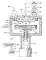
- FIG. 1is a schematic cross-sectional view of a processing chamber that may be used to practice embodiments described herein;
- FIG. 2illustrates a process sequence for tungsten nucleation layer formation using deposition techniques according to embodiments described herein;
- FIGS. 3A-3Bdepict cross-sectional views of a substrate at different stages of an integrated circuit fabrication sequence.
- FIG. 1depicts a schematic cross-sectional view of a chemical vapor deposition (CVD) process chamber 100 that may be used to practice embodiments of the invention described herein.
- the process chamber 100may be part of a processing system (not shown) that includes multiple processing chambers connected to a central transfer chamber (not shown) and serviced by a robot (not shown).
- the process chamber 100includes walls 106 , a bottom 108 , and a lid 110 that define a process volume 112 .
- the walls 106 and bottom 108are typically fabricated from a unitary block of aluminum.
- the walls 106may have conduits (not shown) therein through which a fluid may be passed to control the temperature of the walls 106 .
- the process chamber 100may also include a pumping ring 114 that couples the process volume 112 to an exhaust port 116 as well as other pumping components (not shown).
- a heated support assembly 138is centrally disposed within the process chamber 100 .
- the support assembly 138supports a substrate 300 during a deposition process.
- the support assembly 138generally is fabricated from aluminum, ceramic or a combination of aluminum and ceramic and typically includes a vacuum port (not shown) and at least one or more heating elements 132 .
- the vacuum portmay be used to apply a vacuum between the substrate 300 and the substrate support 138 , so as to secure the substrate 300 to the substrate support 138 during the deposition process.
- the one or more heating elements 132may be, for example, electrodes disposed in the substrate support 138 , and coupled to a power source 130 , to heat the substrate support 138 and substrate 300 positioned thereon to a predetermined temperature.
- the support assembly 138is coupled to a stem 142 .
- the stem 142provides a conduit for electrical leads, vacuum and gas supply lines between the support assembly 138 and other components of the process chamber 100 .
- the stem 142couples the support assembly 138 to a lift system 144 that moves the support assembly 138 between an elevated position (as shown in FIG. 1 ) and a lowered position (not shown).
- Bellows 146provide a vacuum seal between the chamber volume 112 and the atmosphere outside the process chamber 100 while facilitating the movement of the support assembly 138 .
- the support assembly 138additionally supports a circumscribing shadow ring 148 .
- the shadow ring 148is annular in form and typically comprises a ceramic material such as, for example, aluminum nitride. Generally, the shadow ring 148 prevents deposition at the edge of the substrate 300 and support assembly 138 .
- the lid 110is supported by the walls 106 and may be removed to service the process chamber 100 .
- the lid 110is generally comprised of aluminum and may additionally have heat transfer fluid channels 124 formed therein.
- the heat transfer fluid channels 124are coupled to a fluid source (not shown) that flows a heat transfer fluid through the lid 110 . Fluid flowing through the channels 124 regulates the temperature of the lid 110 .
- a mixing block 134is disposed in the lid 110 .
- the mixing block 134is coupled to gas sources 104 .
- individual gas streams from the gas sources 104are combined in the mixing block 134 .
- These gasesare mixed into a single homogeneous gas flow in the mixing block 134 and introduced into the process volume 112 after passing through a showerhead 118 that diffuses the gas flow outwardly towards the chamber walls 106 .
- the showerhead 118is generally coupled to an interior side 120 of the lid 110 .
- a perforated blocker plate 136may optionally be disposed in the plenum 122 between the showerhead 118 and lid 110 .
- Gases (i.e., process and other gases) that enter the process chamber 100 through the mixing block 134are first diffused by the blocker plate 136 as the gases fill the plenum 122 behind the showerhead 118 . The gases then pass through the showerhead 118 and the process chamber 100 .
- the blocker plate 136 and the showerhead 118are configured to provide a uniform flow of gases to the process chamber 100 . Uniform gas flow is desirable to promote uniform layer formation on the substrate 300 .
- the CVD process chamber 100is controlled by a microprocessor controller 154 .
- the microprocessor controllermay be one of any form of general purpose computer processor (CPU) that can be used in an industrial setting for controlling various chambers and sub-processors.
- the computer processormay use any suitable memory, such as random access memory, read only memory, floppy disc drive, hard disk, or any other form of digital storage local or remote.
- Various support circuitsmay be coupled to the CPU for supporting the processor in a conventional manner.
- Software routines as requiredmay be stored in the memory or executed by a second CPU that is remotely located.
- the software routinesare executed after the substrate is positioned on the substrate support.
- the software routineswhen executed, transform the general purpose computer into a specific process computer that controls the chamber operation so that a chamber process is performed.
- the software routinesmay be performed in hardware as an application specific integrated circuit or other type of hardware implementation, or a combination of software and hardware.
- FIG. 2illustrates a process sequence 200 detailing the various steps used for the formation of a tungsten nucleation layer. These steps may be performed in a CVD process chamber similar to that described above with reference to FIG. 1 .
- a substrateis provided to the CVD process chamber.
- the substratemay be, for example, a silicon substrate, which mayor may not have one or more material layers disposed thereon.
- the one or more material layersfor example, may be an oxide layer having a sub-quarter micron aperture therein.
- Sub-quarter micron aperturestypically have aspect ratios (e.g., the feature width divided by the feature length) greater than about 8:1.
- the sub-quarter micron featuresmay have a barrier layer formed therein.
- the barrier layermay be, for example, titanium nitride.
- the barrier layergenerally serves to prevent diffusion of the tungsten into surrounding material layers and to enhance the adhesion of the tungsten layer.
- a tungsten nucleation layeris deposited on the substrate conformably in the sub-quarter micron features.
- the tungsten nucleation layermay be formed, for example, from a reaction of a tungsten-containing precursor such as, for example, tungsten hexafluoride (WF 6 ) with a reducing gas such as for example, silane (SiH 4 ), disilane (Si 2 H 6 ), borane (BH 3 ), and diborane (B 2 H 6 ), among others.
- tungsten hexafluorideis reacted with silane.
- Helium and argon, or other inert gasesmay also be provided along with the reactant gases either singly or in combination.
- the reactionmay be performed at a tungsten hexafluoride flow rate of about 5 sccm (standard cubic centimeters per minute) to about 100 sccm and a silane flow rate of about 1 sccm to about 100 sccm.
- the tungsten-containing precursor and the reducing gasmay be provided to the process chamber in a tungsten-containing precursor to reducing gas ratio of about 1:1 to about 5:1. It is believed that such ratios for the tungsten-containing precursor and the reducing provide good step coverage for the tungsten nucleation layer.
- a total pressure of about 0.5 Torr to about 100 Torr and a pedestal temperature of about 200° C. to about 600° C.may be used.
- the tungsten-containing precursor and the reducing gasmay be flowed or pulsed into the process chamber for a time period of about 0.1 seconds to about 10 seconds, and preferably for about 1 second to about 3 seconds.
- the time period of reactant gas flowshould be generally long enough to provide a sufficiently high deposition rate for the tungsten nucleation layer.
- the process chamberis purged/pumped to remove reaction by-products generated during nucleation layer deposition.
- the production of these reaction by-products at or near the surface of the tungsten nucleation layeris believed to form a rough tungsten surface and contributes to non-conformality and poor step coverage during tungsten nucleation layer deposition. Removal of the reaction by-products using a purge/pump step may provide nucleation layers with improved step coverage.
- the purge gasmay be one or more gases selected from the group of argon, nitrogen (N 2 ), helium, neon, and xenon, among others.
- the process chamberis purged by providing thereto a purge gas at a flow rate of about 5 sccm to about 5000 sccm, for up to about 10 seconds.
- the process chambermay be depressurized in order to remove the residual reactant gases as well as any reaction by-products.
- the depressurization of the process chambermay result in the chamber pressure being reduced to a pressure in a range of about 0.01 Torr to about 40 Torr within a time period of about 0.5 seconds to about 20 seconds.
- excess tungsten-containing precursormay remain in the process chamber after the purge/pump step 206 .
- a flow of the reducing gasmay be provided to the process chamber. The flow of the reducing gas functions to react with excess tungsten-containing precursor that may be present near the surface of the nucleation layer, particularly in regions adjacent to the high aspect ration features after the purge/pump step 208 .
- the reducing gasmay be provided to the process chamber as a pulse or flow for a time period within a range of about 0.1 seconds to about 10 seconds.
- the time periodshould be long enough for the reducing gas to react with excess tungsten-containing precursor in the process chamber.
- it is believed that such flow of reducing gasmay react with any excess tungsten-containing precursor in the vicinity of the feature improving the step coverage therefore and depositing tungsten in a void-free manner within such features.
- the process chamberis purged/pumped to remove reaction by-products as well as residual gases remaining therein.
- the purge gasmay be one or more gases selected from the group of argon, nitrogen, helium, neon, and xenon, among others.
- the process chamberis purged by providing thereto a purge gas at a flow rate of about 5 sccm to about 5000 sccm, for up to about 10 seconds.
- the process chambermay be depressurized in order to remove the residual reactant gases as well as any reaction by-products.
- the depressurization of the process chambermay result in the chamber pressure being reduced to a pressure in a range of about 0.01 Torr to about 40 Torr within a time period of about 0.5 seconds to about 20 seconds.
- steps 204 through 210may be repeated until a desired thickness for the tungsten nucleation layer is achieved. Thereafter, when the desired thickness for the tungsten nucleation layer is achieved the process is stopped as indicated by step 214 .
- the determination of the thickness of the tungsten nucleation layermay be performed using conventional processes such as, for example, spectroscopic measurements.
- the thickness of the nucleation layermay be estimated by performing a calculation based upon the deposition rate as determined using, for example, various process variables such as flow rates, temperature and pressure.
- steps 206 through 210are depicted as three distinct steps in FIG. 2 , steps 206 through 210 may take place simultaneously.
- a purge gasmay be provided to the process chamber simultaneously with the reducing gas to improve overall process throughput.
- process variablessuch the temperature, pressure, gas flow rates, flow/pulse times, and the like, may be adjusted throughout the nucleation layer deposition process in order to optimize layer deposition rate.
- a low ratio for the tungsten-containing precursor and reducing gase.g., ratio of about 1:1
- the ratio for the tungsten-containing precursor and reducing gasmay be increased (e.g., ratio of 3:1).
- a silicon substrate 300 having a feature 310 formed in a dielectric layer 301was provided, as shown in FIG. 3A .
- the substrate 300had a titanium nitride barrier layer 304 conformably deposited on the feature 310 .
- a tungsten nucleation layer 306was formed on the titanium nitride barrier layer within the feature 310 , as shown in FIG. 3B .
- the tungsten nucleation layerwas formed as described above with reference to FIG. 2 .
- a gas mixturecomprising tungsten hexafluoride and silane was provided to the process chamber for a time period of about 1.5 seconds.
- the respective flow rates of the tungsten hexafluoride and silanewere about 30 sccm and about 10 sccm, respectively.
- An argon carrier gaswas provided to the chamber at a flow rate of about 1,500 sccm along with tungsten hexafluoride.
- a nitrogen (N 2 ) carrier gaswas provided to the chamber at a flow rate of about 300 sccm along with the silane.
- the gas mixturewas removed from the process chamber by providing a pulse of argon for a duration of about 2 seconds. Thereafter, a flow of silane gas was provided to the chamber at a flow rate of about 20 sccm for about 1 second. A pulse of argon was then provided for about 2 seconds in order purge the process chamber. This process sequence was repeated by providing the gas mixture, the argon purge, the flow of silane, and the argon purge until a thickness of about 250 ⁇ for the tungsten nucleation layer was achieved. The resulting tungsten nucleation layer had a step coverage, as determined by transmission electron microscopy (TEM) of about 100%.
- TEMtransmission electron microscopy
Landscapes
- Chemical & Material Sciences (AREA)
- Engineering & Computer Science (AREA)
- Materials Engineering (AREA)
- Chemical Kinetics & Catalysis (AREA)
- General Chemical & Material Sciences (AREA)
- Organic Chemistry (AREA)
- Metallurgy (AREA)
- Mechanical Engineering (AREA)
- Crystallography & Structural Chemistry (AREA)
- Computer Hardware Design (AREA)
- Microelectronics & Electronic Packaging (AREA)
- Power Engineering (AREA)
- Manufacturing & Machinery (AREA)
- General Physics & Mathematics (AREA)
- Condensed Matter Physics & Semiconductors (AREA)
- Physics & Mathematics (AREA)
- Chemical Vapour Deposition (AREA)
- Electrodes Of Semiconductors (AREA)
- Internal Circuitry In Semiconductor Integrated Circuit Devices (AREA)
Abstract
Description
This application is a continuation of U.S. Ser. No. 10/194,629 (APPM/005730.Y1), filed Jul. 12, 2002, now issued as U.S. Pat. No. 7,211,144, which is a continuation-in-part of U.S. Ser. No. 10/023,125 (APPM/005730), filed Dec. 17, 2001, now abandoned, which claims benefit of U.S. Ser. No. 60/305,307 (APPM/005730L), filed Jul. 13, 2001, which are herein incorporated by reference in their entirety.
1. Field of the Invention
The present invention generally relates to a method of forming tungsten layers and, more particularly forming tungsten layers using a pulsed nucleation deposition process.
2. Description of the Related Art
Integrated circuits have evolved into complex devices that can include millions of components (e.g., transistors, capacitors and resistors) on a single chip. The evolution of chip designs continually requires faster circuitry and greater circuit density. The demands for greater circuit density necessitate a reduction in the dimensions of the integrated circuit components as well as improved layer uniformity.
In particular, metal layers, such as those used for interconnect, contact, and plug fill applications, are subject to increasingly stringent requirements related to step coverage and layer uniformity. Tungsten layers, for example, are particularly difficult to deposit with uniform step coverage. Typically, tungsten layers are formed by chemical vapor deposition (CVD), using a two step process. A bulk tungsten layer is typically deposited by reacting tungsten hexafluoride (WF6) with hydrogen (H2) on a substrate. In order to reduce the time required to initiate the reaction between the tungsten hexafluoride and the hydrogen (i.e., reduce the “incubation time”), a nucleation layer is typically deposited prior to depositing the bulk tungsten layer. Unfortunately, the nucleation layer, typically deposited by reacting tungsten hexafluoride with silane (SiH4), has sub-optimal step coverage. As a result, voids may form in the tungsten nucleation layer during deposition, adversely impacting the electrical performance of devices fabricated therefrom.
Therefore, a need exists in the art for a method of depositing a tungsten nucleation layer with improved step coverage.
Embodiments of the invention generally relate to a method of forming a tungsten nucleation layer using a sequential deposition process. The tungsten nucleation layer is formed by reacting pulses of a tungsten-containing precursor and a reducing gas in a process chamber to deposit tungsten on the substrate. Thereafter, reaction by-products generated from the tungsten deposition are removed from the process chamber. After the reaction byproducts are removed from the process chamber, a flow of the reducing gas is provided to the process chamber to react with residual tungsten-containing precursor remaining therein. Such a deposition process forms tungsten nucleation layers having good step coverage. The sequential deposition process of reacting pulses of the tungsten-containing precursor and the reducing gas, removing reaction by-products, and than providing a flow of the reducing gas to the process chamber may be repeated until a desired thickness for the tungsten nucleation layer is formed.
The formation of the tungsten nucleation layer is compatible with integrated circuit fabrication processes. In one integrated circuit fabrication process, the tungsten nucleation layer is formed prior to tungsten plug formation. For such an embodiment, a preferred process sequence includes depositing a tungsten nucleation layer in apertures defined in a dielectric material layer formed on a substrate. The tungsten nucleation layer is formed using a sequential deposition process in which pulses of a tungsten-containing precursor and a reducing gas are reacted, reaction by-products removed, and then a flow of reducing gas is provided to a process chamber. The sequential deposition process may be repeated until a desired thickness for the tungsten nucleation layer is deposited. Thereafter, the tungsten plug is completed when a bulk tungsten layer is deposited on the tungsten nucleation layer to fill the apertures.
So that the manner in which the above recited features, advantages and objects of the invention are attained and can be understood in detail, a more particular description of the invention, briefly summarized above, may be had by reference to the embodiments thereof which are illustrated in the appended drawings.
It is to be noted, however, that the appended drawings illustrate only typical embodiments of this invention and are therefore not to be considered limiting of its scope, for the invention may admit to other equally effective embodiments.
Embodiments described herein relate to a method for depositing a tungsten nucleation layer on a substrate.FIG. 1 depicts a schematic cross-sectional view of a chemical vapor deposition (CVD)process chamber 100 that may be used to practice embodiments of the invention described herein. Theprocess chamber 100 may be part of a processing system (not shown) that includes multiple processing chambers connected to a central transfer chamber (not shown) and serviced by a robot (not shown).
Theprocess chamber 100 includeswalls 106, abottom 108, and alid 110 that define aprocess volume 112. Thewalls 106 andbottom 108 are typically fabricated from a unitary block of aluminum. Thewalls 106 may have conduits (not shown) therein through which a fluid may be passed to control the temperature of thewalls 106. Theprocess chamber 100 may also include apumping ring 114 that couples theprocess volume 112 to anexhaust port 116 as well as other pumping components (not shown).
Aheated support assembly 138 is centrally disposed within theprocess chamber 100. Thesupport assembly 138 supports asubstrate 300 during a deposition process. Thesupport assembly 138 generally is fabricated from aluminum, ceramic or a combination of aluminum and ceramic and typically includes a vacuum port (not shown) and at least one ormore heating elements 132.
The vacuum port may be used to apply a vacuum between thesubstrate 300 and thesubstrate support 138, so as to secure thesubstrate 300 to thesubstrate support 138 during the deposition process. The one ormore heating elements 132, may be, for example, electrodes disposed in thesubstrate support 138, and coupled to apower source 130, to heat thesubstrate support 138 andsubstrate 300 positioned thereon to a predetermined temperature.
Generally, thesupport assembly 138 is coupled to astem 142. Thestem 142 provides a conduit for electrical leads, vacuum and gas supply lines between thesupport assembly 138 and other components of theprocess chamber 100. Additionally, thestem 142 couples thesupport assembly 138 to alift system 144 that moves thesupport assembly 138 between an elevated position (as shown inFIG. 1 ) and a lowered position (not shown). Bellows146 provide a vacuum seal between thechamber volume 112 and the atmosphere outside theprocess chamber 100 while facilitating the movement of thesupport assembly 138.
Thesupport assembly 138 additionally supports acircumscribing shadow ring 148. Theshadow ring 148 is annular in form and typically comprises a ceramic material such as, for example, aluminum nitride. Generally, theshadow ring 148 prevents deposition at the edge of thesubstrate 300 andsupport assembly 138.
Thelid 110 is supported by thewalls 106 and may be removed to service theprocess chamber 100. Thelid 110 is generally comprised of aluminum and may additionally have heattransfer fluid channels 124 formed therein. The heattransfer fluid channels 124 are coupled to a fluid source (not shown) that flows a heat transfer fluid through thelid 110. Fluid flowing through thechannels 124 regulates the temperature of thelid 110.
A mixingblock 134 is disposed in thelid 110. The mixingblock 134 is coupled togas sources 104. Generally, individual gas streams from thegas sources 104 are combined in themixing block 134. These gases are mixed into a single homogeneous gas flow in themixing block 134 and introduced into theprocess volume 112 after passing through ashowerhead 118 that diffuses the gas flow outwardly towards thechamber walls 106.
Theshowerhead 118 is generally coupled to aninterior side 120 of thelid 110. Aperforated blocker plate 136 may optionally be disposed in theplenum 122 between theshowerhead 118 andlid 110. Gases (i.e., process and other gases) that enter theprocess chamber 100 through the mixingblock 134 are first diffused by theblocker plate 136 as the gases fill theplenum 122 behind theshowerhead 118. The gases then pass through theshowerhead 118 and theprocess chamber 100. Theblocker plate 136 and theshowerhead 118 are configured to provide a uniform flow of gases to theprocess chamber 100. Uniform gas flow is desirable to promote uniform layer formation on thesubstrate 300.
TheCVD process chamber 100 is controlled by amicroprocessor controller 154. The microprocessor controller may be one of any form of general purpose computer processor (CPU) that can be used in an industrial setting for controlling various chambers and sub-processors. The computer processor may use any suitable memory, such as random access memory, read only memory, floppy disc drive, hard disk, or any other form of digital storage local or remote. Various support circuits may be coupled to the CPU for supporting the processor in a conventional manner. Software routines as required may be stored in the memory or executed by a second CPU that is remotely located.
The software routines are executed after the substrate is positioned on the substrate support. The software routines, when executed, transform the general purpose computer into a specific process computer that controls the chamber operation so that a chamber process is performed. Alternatively, the software routines may be performed in hardware as an application specific integrated circuit or other type of hardware implementation, or a combination of software and hardware.
Tungsten Nucleation Layer Formation
The sub-quarter micron features may have a barrier layer formed therein. The barrier layer may be, for example, titanium nitride. The barrier layer generally serves to prevent diffusion of the tungsten into surrounding material layers and to enhance the adhesion of the tungsten layer.
Instep 204, a tungsten nucleation layer is deposited on the substrate conformably in the sub-quarter micron features. The tungsten nucleation layer may be formed, for example, from a reaction of a tungsten-containing precursor such as, for example, tungsten hexafluoride (WF6) with a reducing gas such as for example, silane (SiH4), disilane (Si2H6), borane (BH3), and diborane (B2H6), among others. In one embodiment, tungsten hexafluoride is reacted with silane. Helium and argon, or other inert gases, may also be provided along with the reactant gases either singly or in combination.
Typically, the reaction may be performed at a tungsten hexafluoride flow rate of about 5 sccm (standard cubic centimeters per minute) to about 100 sccm and a silane flow rate of about 1 sccm to about 100 sccm. The tungsten-containing precursor and the reducing gas may be provided to the process chamber in a tungsten-containing precursor to reducing gas ratio of about 1:1 to about 5:1. It is believed that such ratios for the tungsten-containing precursor and the reducing provide good step coverage for the tungsten nucleation layer. A total pressure of about 0.5 Torr to about 100 Torr and a pedestal temperature of about 200° C. to about 600° C. may be used.
The tungsten-containing precursor and the reducing gas may be flowed or pulsed into the process chamber for a time period of about 0.1 seconds to about 10 seconds, and preferably for about 1 second to about 3 seconds. The time period of reactant gas flow should be generally long enough to provide a sufficiently high deposition rate for the tungsten nucleation layer.
Referring to step206, after the flow or pulse of the reactant gases has ceased, the process chamber is purged/pumped to remove reaction by-products generated during nucleation layer deposition. The production of these reaction by-products at or near the surface of the tungsten nucleation layer is believed to form a rough tungsten surface and contributes to non-conformality and poor step coverage during tungsten nucleation layer deposition. Removal of the reaction by-products using a purge/pump step may provide nucleation layers with improved step coverage.
The purge gas may be one or more gases selected from the group of argon, nitrogen (N2), helium, neon, and xenon, among others. Typically, the process chamber is purged by providing thereto a purge gas at a flow rate of about 5 sccm to about 5000 sccm, for up to about 10 seconds.
Alternatively or in addition to introducing the purge gas, the process chamber may be depressurized in order to remove the residual reactant gases as well as any reaction by-products. The depressurization of the process chamber may result in the chamber pressure being reduced to a pressure in a range of about 0.01 Torr to about 40 Torr within a time period of about 0.5 seconds to about 20 seconds.
Depending upon the ratio of the tungsten-containing precursor to the reducing gas in the reactant gas mixture, as well as the removal time, excess tungsten-containing precursor may remain in the process chamber after the purge/pump step 206. Referring to step208, after the purge/pump step is performed, a flow of the reducing gas may be provided to the process chamber. The flow of the reducing gas functions to react with excess tungsten-containing precursor that may be present near the surface of the nucleation layer, particularly in regions adjacent to the high aspect ration features after the purge/pump step 208.
The reducing gas may be provided to the process chamber as a pulse or flow for a time period within a range of about 0.1 seconds to about 10 seconds. In general, the time period should be long enough for the reducing gas to react with excess tungsten-containing precursor in the process chamber. Particularly for high aspect ratio features, it is believed that such flow of reducing gas may react with any excess tungsten-containing precursor in the vicinity of the feature improving the step coverage therefore and depositing tungsten in a void-free manner within such features.
Referring to step210, after the flow or pulse of the reducing gas has ceased, the process chamber is purged/pumped to remove reaction by-products as well as residual gases remaining therein. The purge gas may be one or more gases selected from the group of argon, nitrogen, helium, neon, and xenon, among others. Typically, the process chamber is purged by providing thereto a purge gas at a flow rate of about 5 sccm to about 5000 sccm, for up to about 10 seconds.
Alternatively or in addition to introducing the purge gas, the process chamber may be depressurized in order to remove the residual reactant gases as well as any reaction by-products. The depressurization of the process chamber may result in the chamber pressure being reduced to a pressure in a range of about 0.01 Torr to about 40 Torr within a time period of about 0.5 seconds to about 20 seconds.
Referring to step212, after purge/pump step 210, a total thickness of the tungsten nucleation layer will be formed on the substrate. Depending on specific device requirements,steps 204 through210 may be repeated until a desired thickness for the tungsten nucleation layer is achieved. Thereafter, when the desired thickness for the tungsten nucleation layer is achieved the process is stopped as indicated bystep 214.
The determination of the thickness of the tungsten nucleation layer may be performed using conventional processes such as, for example, spectroscopic measurements. Alternatively, the thickness of the nucleation layer may be estimated by performing a calculation based upon the deposition rate as determined using, for example, various process variables such as flow rates, temperature and pressure.
Whilesteps 206 through210 are depicted as three distinct steps inFIG. 2 ,steps 206 through210 may take place simultaneously. For example, a purge gas may be provided to the process chamber simultaneously with the reducing gas to improve overall process throughput.
Additionally, process variables, such the temperature, pressure, gas flow rates, flow/pulse times, and the like, may be adjusted throughout the nucleation layer deposition process in order to optimize layer deposition rate. For example, early in the deposition process, a low ratio for the tungsten-containing precursor and reducing gas (e.g., ratio of about 1:1) may be used instep 204 in order to, for example, minimize the adverse effects of fluorine on underlying material layers. In subsequent deposition cycles, the ratio for the tungsten-containing precursor and reducing gas may be increased (e.g., ratio of 3:1).
In an exemplary tungsten nucleation layer deposition process, asilicon substrate 300 having afeature 310 formed in adielectric layer 301 was provided, as shown inFIG. 3A . Thesubstrate 300 had a titaniumnitride barrier layer 304 conformably deposited on thefeature 310. Atungsten nucleation layer 306 was formed on the titanium nitride barrier layer within thefeature 310, as shown inFIG. 3B . The tungsten nucleation layer was formed as described above with reference toFIG. 2 .
Specifically, a gas mixture comprising tungsten hexafluoride and silane was provided to the process chamber for a time period of about 1.5 seconds. The respective flow rates of the tungsten hexafluoride and silane were about 30 sccm and about 10 sccm, respectively. An argon carrier gas was provided to the chamber at a flow rate of about 1,500 sccm along with tungsten hexafluoride. A nitrogen (N2) carrier gas was provided to the chamber at a flow rate of about 300 sccm along with the silane.
The gas mixture was removed from the process chamber by providing a pulse of argon for a duration of about 2 seconds. Thereafter, a flow of silane gas was provided to the chamber at a flow rate of about 20 sccm for about 1 second. A pulse of argon was then provided for about 2 seconds in order purge the process chamber. This process sequence was repeated by providing the gas mixture, the argon purge, the flow of silane, and the argon purge until a thickness of about 250 Å for the tungsten nucleation layer was achieved. The resulting tungsten nucleation layer had a step coverage, as determined by transmission electron microscopy (TEM) of about 100%.
While the foregoing is directed to embodiments of the invention, other and further embodiments of the invention may be devised without departing from the basic scope thereof, and the scope thereof is determined by the claims that follow.
Claims (30)
1. A method for depositing a tungsten material on a substrate within a process chamber, comprising:
exposing a substrate within a process chamber simultaneously to a tungsten precursor and a reducing gas to deposit a tungsten nucleation layer on the substrate during a tungsten deposition process;
removing reaction by-products generated during the tungsten deposition process from the process chamber;
exposing the substrate to the reducing gas to react with residual tungsten precursor within the process chamber during a soak process;
removing reaction by-products generated during the soak process from the process chamber; and
repeating the tungsten deposition process and the soak process during a cyclic deposition process.
2. The method ofclaim 1 , wherein the reducing gas comprises a reducing agent selected from the group consisting of silane, disilane, borane, diborane, derivatives thereof, and combinations thereof.
3. The method ofclaim 2 , wherein the tungsten precursor comprises tungsten hexafluoride.
4. The method ofclaim 3 , wherein the cyclic deposition process is repeated until the tungsten nucleation layer has a thickness of about 500 Å.
5. The method ofclaim 3 , wherein the tungsten nucleation layer is deposited on a barrier layer comprising titanium nitride.
6. The method ofclaim 1 , wherein the tungsten deposition process lasts for a time period within a range from about 0.1 seconds to about 10 seconds.
7. The method ofclaim 6 , wherein the time period lasts about 3 seconds or less.
8. The method ofclaim 7 , wherein the time period lasts about 1 second or less.
9. The method ofclaim 1 , wherein the soak process lasts for a time period of up to about 10 seconds.
10. The method ofclaim 9 , wherein the reducing gas comprises diborane.
11. The method ofclaim 9 , wherein the reducing gas comprises silane.
12. The method ofclaim 1 , wherein the removing reaction by-products generated during the tungsten deposition process overlaps in time with the soak process.
13. A method for depositing a tungsten material on a substrate within a process chamber, comprising:
exposing a substrate within a process chamber simultaneously to a tungsten precursor and a reducing gas to deposit a tungsten nucleation layer on the substrate during a tungsten deposition process, wherein the reducing gas comprises diborane;
removing reaction by-products generated during the tungsten deposition process from the process chamber;
exposing the substrate to the reducing gas to react with residual tungsten precursor within the process chamber during a soak process;
removing reaction by-products generated during the soak process from the process chamber; and
repeating the tungsten deposition process and the soak process during a cyclic deposition process.
14. The method ofclaim 13 , wherein the tungsten precursor comprises tungsten hexafluoride.
15. The method ofclaim 14 , wherein the cyclic deposition process is repeated until the tungsten nucleation layer has a thickness of about 500 Å.
16. The method ofclaim 14 , wherein the tungsten nucleation layer is deposited on a barrier layer comprising titanium nitride.
17. The method ofclaim 13 , wherein the tungsten deposition process lasts for a time period within a range from about 0.1 seconds to about 10 seconds.
18. The method ofclaim 17 , wherein the time period lasts about 3 seconds or less.
19. The method ofclaim 18 , wherein the time period lasts about 1 second or less.
20. The method ofclaim 13 , wherein the soak process lasts for a time period of up to about 10 seconds.
21. The method ofclaim 13 , wherein the removing reaction by-products generated during the tungsten deposition process overlaps in time with the soak process.
22. A method for depositing a tungsten material on a substrate within a process chamber, comprising:
exposing a substrate within a process chamber simultaneously to a tungsten precursor and a reducing gas to deposit a tungsten nucleation layer on the substrate during a tungsten deposition process, wherein the reducing gas comprises silane;
removing reaction by-products generated during the tungsten deposition process from the process chamber;
exposing the substrate to the reducing gas to react with residual tungsten precursor within the process chamber during a soak process;
removing reaction by-products generated during the soak process from the process chamber; and
repeating the tungsten deposition process and the soak process during a cyclic deposition process.
23. The method ofclaim 22 , wherein the tungsten precursor comprises tungsten hexafluoride.
24. The method ofclaim 23 , wherein the cyclic deposition process is repeated until the tungsten nucleation layer has a thickness of about 500 Å.
25. The method ofclaim 23 , wherein the tungsten nucleation layer is deposited on a barrier layer comprising titanium nitride.
26. The method ofclaim 22 , wherein the tungsten deposition process lasts for a time period within a range from about 0.1 seconds to about 10 seconds.
27. The method ofclaim 26 , wherein the time period lasts about 3 seconds or less.
28. The method ofclaim 27 , wherein the time period lasts about 1 second or less.
29. The method ofclaim 22 , wherein the soak process lasts for a time period of up to about 10 seconds.
30. The method ofclaim 22 , wherein the removing reaction by-products generated during the tungsten deposition process overlaps in time with the soak process.
Priority Applications (1)
| Application Number | Priority Date | Filing Date | Title |
|---|---|---|---|
| US11/621,040US7695563B2 (en) | 2001-07-13 | 2007-01-08 | Pulsed deposition process for tungsten nucleation |
Applications Claiming Priority (4)
| Application Number | Priority Date | Filing Date | Title |
|---|---|---|---|
| US30530701P | 2001-07-13 | 2001-07-13 | |
| US10/023,125US20070009658A1 (en) | 2001-07-13 | 2001-12-17 | Pulse nucleation enhanced nucleation technique for improved step coverage and better gap fill for WCVD process |
| US10/194,629US7211144B2 (en) | 2001-07-13 | 2002-07-12 | Pulsed nucleation deposition of tungsten layers |
| US11/621,040US7695563B2 (en) | 2001-07-13 | 2007-01-08 | Pulsed deposition process for tungsten nucleation |
Related Parent Applications (1)
| Application Number | Title | Priority Date | Filing Date |
|---|---|---|---|
| US10/194,629ContinuationUS7211144B2 (en) | 2001-07-13 | 2002-07-12 | Pulsed nucleation deposition of tungsten layers |
Publications (2)
| Publication Number | Publication Date |
|---|---|
| US20080317954A1 US20080317954A1 (en) | 2008-12-25 |
| US7695563B2true US7695563B2 (en) | 2010-04-13 |
Family
ID=30114793
Family Applications (2)
| Application Number | Title | Priority Date | Filing Date |
|---|---|---|---|
| US10/194,629Expired - LifetimeUS7211144B2 (en) | 2001-07-13 | 2002-07-12 | Pulsed nucleation deposition of tungsten layers |
| US11/621,040Expired - Fee RelatedUS7695563B2 (en) | 2001-07-13 | 2007-01-08 | Pulsed deposition process for tungsten nucleation |
Family Applications Before (1)
| Application Number | Title | Priority Date | Filing Date |
|---|---|---|---|
| US10/194,629Expired - LifetimeUS7211144B2 (en) | 2001-07-13 | 2002-07-12 | Pulsed nucleation deposition of tungsten layers |
Country Status (3)
| Country | Link |
|---|---|
| US (2) | US7211144B2 (en) |
| JP (1) | JP2005533181A (en) |
| WO (1) | WO2004007794A2 (en) |
Cited By (26)
| Publication number | Priority date | Publication date | Assignee | Title |
|---|---|---|---|---|
| US20100267235A1 (en)* | 2009-04-16 | 2010-10-21 | Feng Chen | Methods for depositing ultra thin low resistivity tungsten film for small critical dimension contacts and interconnects |
| US7846840B2 (en)* | 2000-06-28 | 2010-12-07 | Applied Materials, Inc. | Method for forming tungsten materials during vapor deposition processes |
| US8853080B2 (en) | 2012-09-09 | 2014-10-07 | Novellus Systems, Inc. | Method for depositing tungsten film with low roughness and low resistivity |
| US8859417B2 (en) | 2013-01-03 | 2014-10-14 | Globalfoundries Inc. | Gate electrode(s) and contact structure(s), and methods of fabrication thereof |
| US9076843B2 (en) | 2001-05-22 | 2015-07-07 | Novellus Systems, Inc. | Method for producing ultra-thin tungsten layers with improved step coverage |
| US9153486B2 (en) | 2013-04-12 | 2015-10-06 | Lam Research Corporation | CVD based metal/semiconductor OHMIC contact for high volume manufacturing applications |
| US9159571B2 (en) | 2009-04-16 | 2015-10-13 | Lam Research Corporation | Tungsten deposition process using germanium-containing reducing agent |
| US9240347B2 (en) | 2012-03-27 | 2016-01-19 | Novellus Systems, Inc. | Tungsten feature fill |
| US9589808B2 (en) | 2013-12-19 | 2017-03-07 | Lam Research Corporation | Method for depositing extremely low resistivity tungsten |
| US9613818B2 (en) | 2015-05-27 | 2017-04-04 | Lam Research Corporation | Deposition of low fluorine tungsten by sequential CVD process |
| US9754824B2 (en) | 2015-05-27 | 2017-09-05 | Lam Research Corporation | Tungsten films having low fluorine content |
| US9953984B2 (en) | 2015-02-11 | 2018-04-24 | Lam Research Corporation | Tungsten for wordline applications |
| US9978605B2 (en) | 2015-05-27 | 2018-05-22 | Lam Research Corporation | Method of forming low resistivity fluorine free tungsten film without nucleation |
| US9997405B2 (en) | 2014-09-30 | 2018-06-12 | Lam Research Corporation | Feature fill with nucleation inhibition |
| US10256142B2 (en) | 2009-08-04 | 2019-04-09 | Novellus Systems, Inc. | Tungsten feature fill with nucleation inhibition |
| US10636705B1 (en) | 2018-11-29 | 2020-04-28 | Applied Materials, Inc. | High pressure annealing of metal gate structures |
| US11348795B2 (en) | 2017-08-14 | 2022-05-31 | Lam Research Corporation | Metal fill process for three-dimensional vertical NAND wordline |
| US11549175B2 (en) | 2018-05-03 | 2023-01-10 | Lam Research Corporation | Method of depositing tungsten and other metals in 3D NAND structures |
| US11705337B2 (en) | 2017-05-25 | 2023-07-18 | Applied Materials, Inc. | Tungsten defluorination by high pressure treatment |
| US20230340662A1 (en)* | 2022-04-26 | 2023-10-26 | Applied Materials, Inc. | Gas delivery for tungsten-containing layer |
| US11972952B2 (en) | 2018-12-14 | 2024-04-30 | Lam Research Corporation | Atomic layer deposition on 3D NAND structures |
| US11976002B2 (en) | 2021-01-05 | 2024-05-07 | Applied Materials, Inc. | Methods for encapsulating silver mirrors on optical structures |
| US12002679B2 (en) | 2019-04-11 | 2024-06-04 | Lam Research Corporation | High step coverage tungsten deposition |
| US12077858B2 (en) | 2019-08-12 | 2024-09-03 | Lam Research Corporation | Tungsten deposition |
| US12237221B2 (en) | 2019-05-22 | 2025-02-25 | Lam Research Corporation | Nucleation-free tungsten deposition |
| US12444651B2 (en) | 2022-06-28 | 2025-10-14 | Novellus Systems, Inc. | Tungsten feature fill with nucleation inhibition |
Families Citing this family (101)
| Publication number | Priority date | Publication date | Assignee | Title |
|---|---|---|---|---|
| FI119941B (en)* | 1999-10-15 | 2009-05-15 | Asm Int | Process for the preparation of nanolaminates |
| US6482262B1 (en) | 1959-10-10 | 2002-11-19 | Asm Microchemistry Oy | Deposition of transition metal carbides |
| US6974766B1 (en) | 1998-10-01 | 2005-12-13 | Applied Materials, Inc. | In situ deposition of a low κ dielectric layer, barrier layer, etch stop, and anti-reflective coating for damascene application |
| WO2001029893A1 (en) | 1999-10-15 | 2001-04-26 | Asm America, Inc. | Method for depositing nanolaminate thin films on sensitive surfaces |
| FI20000099A0 (en) | 2000-01-18 | 2000-01-18 | Asm Microchemistry Ltd | A method for growing thin metal films |
| US6620723B1 (en) | 2000-06-27 | 2003-09-16 | Applied Materials, Inc. | Formation of boride barrier layers using chemisorption techniques |
| US7964505B2 (en) | 2005-01-19 | 2011-06-21 | Applied Materials, Inc. | Atomic layer deposition of tungsten materials |
| US7732327B2 (en) | 2000-06-28 | 2010-06-08 | Applied Materials, Inc. | Vapor deposition of tungsten materials |
| US7405158B2 (en) | 2000-06-28 | 2008-07-29 | Applied Materials, Inc. | Methods for depositing tungsten layers employing atomic layer deposition techniques |
| US7101795B1 (en) | 2000-06-28 | 2006-09-05 | Applied Materials, Inc. | Method and apparatus for depositing refractory metal layers employing sequential deposition techniques to form a nucleation layer |
| US6936538B2 (en) | 2001-07-16 | 2005-08-30 | Applied Materials, Inc. | Method and apparatus for depositing tungsten after surface treatment to improve film characteristics |
| US6951804B2 (en)* | 2001-02-02 | 2005-10-04 | Applied Materials, Inc. | Formation of a tantalum-nitride layer |
| US7955972B2 (en) | 2001-05-22 | 2011-06-07 | Novellus Systems, Inc. | Methods for growing low-resistivity tungsten for high aspect ratio and small features |
| US7141494B2 (en)* | 2001-05-22 | 2006-11-28 | Novellus Systems, Inc. | Method for reducing tungsten film roughness and improving step coverage |
| US7589017B2 (en)* | 2001-05-22 | 2009-09-15 | Novellus Systems, Inc. | Methods for growing low-resistivity tungsten film |
| US7262125B2 (en)* | 2001-05-22 | 2007-08-28 | Novellus Systems, Inc. | Method of forming low-resistivity tungsten interconnects |
| US7005372B2 (en) | 2003-01-21 | 2006-02-28 | Novellus Systems, Inc. | Deposition of tungsten nitride |
| US7211144B2 (en) | 2001-07-13 | 2007-05-01 | Applied Materials, Inc. | Pulsed nucleation deposition of tungsten layers |
| TW581822B (en) | 2001-07-16 | 2004-04-01 | Applied Materials Inc | Formation of composite tungsten films |
| US20030029715A1 (en) | 2001-07-25 | 2003-02-13 | Applied Materials, Inc. | An Apparatus For Annealing Substrates In Physical Vapor Deposition Systems |
| JP4938962B2 (en) | 2001-09-14 | 2012-05-23 | エーエスエム インターナショナル エヌ.ヴェー. | Metal nitride deposition by ALD using gettering reactant |
| US6936906B2 (en) | 2001-09-26 | 2005-08-30 | Applied Materials, Inc. | Integration of barrier layer and seed layer |
| US6833161B2 (en) | 2002-02-26 | 2004-12-21 | Applied Materials, Inc. | Cyclical deposition of tungsten nitride for metal oxide gate electrode |
| US7279432B2 (en) | 2002-04-16 | 2007-10-09 | Applied Materials, Inc. | System and method for forming an integrated barrier layer |
| US7398090B2 (en)* | 2002-09-13 | 2008-07-08 | Hewlett-Packard Development Company, L.P. | Defining a smart area |
| US6844258B1 (en) | 2003-05-09 | 2005-01-18 | Novellus Systems, Inc. | Selective refractory metal and nitride capping |
| US7211508B2 (en) | 2003-06-18 | 2007-05-01 | Applied Materials, Inc. | Atomic layer deposition of tantalum based barrier materials |
| US7754604B2 (en)* | 2003-08-26 | 2010-07-13 | Novellus Systems, Inc. | Reducing silicon attack and improving resistivity of tungsten nitride film |
| US7405143B2 (en) | 2004-03-25 | 2008-07-29 | Asm International N.V. | Method for fabricating a seed layer |
| JP2006324610A (en)* | 2005-05-20 | 2006-11-30 | Matsushita Electric Ind Co Ltd | Substrate processing apparatus and substrate processing method |
| JP2007046134A (en)* | 2005-08-11 | 2007-02-22 | Tokyo Electron Ltd | Method for forming metallic film, and recording medium with program recorded therein |
| US20070065597A1 (en)* | 2005-09-15 | 2007-03-22 | Asm Japan K.K. | Plasma CVD film formation apparatus provided with mask |
| US8993055B2 (en) | 2005-10-27 | 2015-03-31 | Asm International N.V. | Enhanced thin film deposition |
| TWI332532B (en) | 2005-11-04 | 2010-11-01 | Applied Materials Inc | Apparatus and process for plasma-enhanced atomic layer deposition |
| KR100651602B1 (en)* | 2005-12-14 | 2006-11-30 | 동부일렉트로닉스 주식회사 | Metal wiring formation method of semiconductor device |
| JP2007194468A (en)* | 2006-01-20 | 2007-08-02 | Renesas Technology Corp | Semiconductor device, and method of manufacturing same |
| US8268409B2 (en)* | 2006-10-25 | 2012-09-18 | Asm America, Inc. | Plasma-enhanced deposition of metal carbide films |
| US7611751B2 (en) | 2006-11-01 | 2009-11-03 | Asm America, Inc. | Vapor deposition of metal carbide films |
| US7713874B2 (en)* | 2007-05-02 | 2010-05-11 | Asm America, Inc. | Periodic plasma annealing in an ALD-type process |
| KR100890047B1 (en)* | 2007-06-28 | 2009-03-25 | 주식회사 하이닉스반도체 | Wiring Formation Method of Semiconductor Device |
| US7655567B1 (en) | 2007-07-24 | 2010-02-02 | Novellus Systems, Inc. | Methods for improving uniformity and resistivity of thin tungsten films |
| WO2009064530A2 (en)* | 2007-08-30 | 2009-05-22 | Washington State University Research Foundation | Semiconductive materials and associated uses thereof |
| US7772114B2 (en)* | 2007-12-05 | 2010-08-10 | Novellus Systems, Inc. | Method for improving uniformity and adhesion of low resistivity tungsten film |
| US8053365B2 (en)* | 2007-12-21 | 2011-11-08 | Novellus Systems, Inc. | Methods for forming all tungsten contacts and lines |
| US8062977B1 (en) | 2008-01-31 | 2011-11-22 | Novellus Systems, Inc. | Ternary tungsten-containing resistive thin films |
| KR101540077B1 (en)* | 2008-04-16 | 2015-07-28 | 에이에스엠 아메리카, 인코포레이티드 | Atomic layer deposition of metal carbide films using aluminum hydrocarbon compounds |
| US7666474B2 (en) | 2008-05-07 | 2010-02-23 | Asm America, Inc. | Plasma-enhanced pulsed deposition of metal carbide films |
| US8058170B2 (en)* | 2008-06-12 | 2011-11-15 | Novellus Systems, Inc. | Method for depositing thin tungsten film with low resistivity and robust micro-adhesion characteristics |
| US8551885B2 (en)* | 2008-08-29 | 2013-10-08 | Novellus Systems, Inc. | Method for reducing tungsten roughness and improving reflectivity |
| WO2010077847A2 (en)* | 2008-12-31 | 2010-07-08 | Applied Materials, Inc. | Method of depositing tungsten film with reduced resistivity and improved surface morphology |
| US8193089B2 (en)* | 2009-07-13 | 2012-06-05 | Seagate Technology Llc | Conductive via plug formation |
| US8207062B2 (en)* | 2009-09-09 | 2012-06-26 | Novellus Systems, Inc. | Method for improving adhesion of low resistivity tungsten/tungsten nitride layers |
| WO2011049816A2 (en) | 2009-10-20 | 2011-04-28 | Asm International N.V. | Processes for passivating dielectric films |
| US8709948B2 (en)* | 2010-03-12 | 2014-04-29 | Novellus Systems, Inc. | Tungsten barrier and seed for copper filled TSV |
| US9129945B2 (en)* | 2010-03-24 | 2015-09-08 | Applied Materials, Inc. | Formation of liner and barrier for tungsten as gate electrode and as contact plug to reduce resistance and enhance device performance |
| US20120199887A1 (en)* | 2011-02-03 | 2012-08-09 | Lana Chan | Methods of controlling tungsten film properties |
| AU2012271612B2 (en) | 2011-06-16 | 2017-08-31 | Zimmer, Inc. | Chemical vapor infiltration apparatus and process |
| AU2012271616B2 (en) | 2011-06-16 | 2015-05-07 | Zimmer, Inc. | Micro-alloyed porous metal having optimized chemical composition and method of manufacturing the same |
| KR101306811B1 (en) | 2012-05-09 | 2013-09-10 | 한국화학연구원 | Novel tungsten aminoamide halide compounds, preparation method thereof and process for the formation of thin films using the same |
| KR101306813B1 (en) | 2012-05-09 | 2013-09-10 | 한국화학연구원 | Novel tungsten aminoamide azide compounds, preparation method thereof and process for the formation of thin films using the same |
| KR101306812B1 (en) | 2012-05-09 | 2013-09-10 | 한국화학연구원 | Novel tungsten silylamide compounds, preparation method thereof and process for the formation of thin films using the same |
| US9034760B2 (en) | 2012-06-29 | 2015-05-19 | Novellus Systems, Inc. | Methods of forming tensile tungsten films and compressive tungsten films |
| US8975184B2 (en) | 2012-07-27 | 2015-03-10 | Novellus Systems, Inc. | Methods of improving tungsten contact resistance in small critical dimension features |
| US9169556B2 (en) | 2012-10-11 | 2015-10-27 | Applied Materials, Inc. | Tungsten growth modulation by controlling surface composition |
| US9412602B2 (en) | 2013-03-13 | 2016-08-09 | Asm Ip Holding B.V. | Deposition of smooth metal nitride films |
| US8846550B1 (en) | 2013-03-14 | 2014-09-30 | Asm Ip Holding B.V. | Silane or borane treatment of metal thin films |
| US8841182B1 (en) | 2013-03-14 | 2014-09-23 | Asm Ip Holding B.V. | Silane and borane treatments for titanium carbide films |
| US9394609B2 (en) | 2014-02-13 | 2016-07-19 | Asm Ip Holding B.V. | Atomic layer deposition of aluminum fluoride thin films |
| US10643925B2 (en) | 2014-04-17 | 2020-05-05 | Asm Ip Holding B.V. | Fluorine-containing conductive films |
| US9595470B2 (en)* | 2014-05-09 | 2017-03-14 | Lam Research Corporation | Methods of preparing tungsten and tungsten nitride thin films using tungsten chloride precursor |
| US10002936B2 (en) | 2014-10-23 | 2018-06-19 | Asm Ip Holding B.V. | Titanium aluminum and tantalum aluminum thin films |
| US9941425B2 (en) | 2015-10-16 | 2018-04-10 | Asm Ip Holdings B.V. | Photoactive devices and materials |
| US9786492B2 (en) | 2015-11-12 | 2017-10-10 | Asm Ip Holding B.V. | Formation of SiOCN thin films |
| US9786491B2 (en) | 2015-11-12 | 2017-10-10 | Asm Ip Holding B.V. | Formation of SiOCN thin films |
| KR102378021B1 (en) | 2016-05-06 | 2022-03-23 | 에이에스엠 아이피 홀딩 비.브이. | Formation of SiOC thin films |
| US10186420B2 (en) | 2016-11-29 | 2019-01-22 | Asm Ip Holding B.V. | Formation of silicon-containing thin films |
| CN110731003B (en) | 2017-04-10 | 2024-03-26 | 朗姆研究公司 | Low resistivity film containing molybdenum |
| US10847529B2 (en) | 2017-04-13 | 2020-11-24 | Asm Ip Holding B.V. | Substrate processing method and device manufactured by the same |
| JP6788545B2 (en) | 2017-04-26 | 2020-11-25 | 東京エレクトロン株式会社 | How to form a tungsten film |
| US10504901B2 (en) | 2017-04-26 | 2019-12-10 | Asm Ip Holding B.V. | Substrate processing method and device manufactured using the same |
| CN114875388A (en) | 2017-05-05 | 2022-08-09 | Asm Ip 控股有限公司 | Plasma enhanced deposition method for controlled formation of oxygen-containing films |
| US10276411B2 (en) | 2017-08-18 | 2019-04-30 | Applied Materials, Inc. | High pressure and high temperature anneal chamber |
| TWI761636B (en) | 2017-12-04 | 2022-04-21 | 荷蘭商Asm Ip控股公司 | PLASMA ENHANCED ATOMIC LAYER DEPOSITION PROCESS AND METHOD OF DEPOSITING SiOC THIN FILM |
| US10633740B2 (en) | 2018-03-19 | 2020-04-28 | Applied Materials, Inc. | Methods for depositing coatings on aerospace components |
| US11015252B2 (en) | 2018-04-27 | 2021-05-25 | Applied Materials, Inc. | Protection of components from corrosion |
| US12014928B2 (en) | 2018-07-31 | 2024-06-18 | Lam Research Corporation | Multi-layer feature fill |
| US11009339B2 (en) | 2018-08-23 | 2021-05-18 | Applied Materials, Inc. | Measurement of thickness of thermal barrier coatings using 3D imaging and surface subtraction methods for objects with complex geometries |
| CN113366144B (en) | 2019-01-28 | 2023-07-07 | 朗姆研究公司 | Deposition of metal films |
| US12359315B2 (en) | 2019-02-14 | 2025-07-15 | Asm Ip Holding B.V. | Deposition of oxides and nitrides |
| EP3959356A4 (en) | 2019-04-26 | 2023-01-18 | Applied Materials, Inc. | Methods of protecting aerospace components against corrosion and oxidation |
| US11794382B2 (en) | 2019-05-16 | 2023-10-24 | Applied Materials, Inc. | Methods for depositing anti-coking protective coatings on aerospace components |
| US11697879B2 (en) | 2019-06-14 | 2023-07-11 | Applied Materials, Inc. | Methods for depositing sacrificial coatings on aerospace components |
| US11466364B2 (en) | 2019-09-06 | 2022-10-11 | Applied Materials, Inc. | Methods for forming protective coatings containing crystallized aluminum oxide |
| US12327762B2 (en) | 2019-10-15 | 2025-06-10 | Lam Research Corporation | Molybdenum fill |
| US12142479B2 (en) | 2020-01-17 | 2024-11-12 | Asm Ip Holding B.V. | Formation of SiOCN thin films |
| US12341005B2 (en) | 2020-01-17 | 2025-06-24 | Asm Ip Holding B.V. | Formation of SiCN thin films |
| US11519066B2 (en) | 2020-05-21 | 2022-12-06 | Applied Materials, Inc. | Nitride protective coatings on aerospace components and methods for making the same |
| TW202200828A (en) | 2020-06-24 | 2022-01-01 | 荷蘭商Asm Ip私人控股有限公司 | Vapor deposition of films comprising molybdenum |
| WO2022005696A1 (en) | 2020-07-03 | 2022-01-06 | Applied Materials, Inc. | Methods for refurbishing aerospace components |
| US12104243B2 (en) | 2021-06-16 | 2024-10-01 | Applied Materials, Inc. | Methods and apparatus for processing a substrate |
| US11721566B2 (en)* | 2021-07-13 | 2023-08-08 | Applied Materials, Inc. | Sensor assembly and methods of vapor monitoring in process chambers |
Citations (332)
| Publication number | Priority date | Publication date | Assignee | Title |
|---|---|---|---|---|
| US3785862A (en) | 1970-12-14 | 1974-01-15 | Rca Corp | Method for depositing refractory metals |
| US4058430A (en) | 1974-11-29 | 1977-11-15 | Tuomo Suntola | Method for producing compound thin films |
| US4389973A (en) | 1980-03-18 | 1983-06-28 | Oy Lohja Ab | Apparatus for performing growth of compound thin films |
| US4413022A (en) | 1979-02-28 | 1983-11-01 | Canon Kabushiki Kaisha | Method for performing growth of compound thin films |
| US4486487A (en) | 1982-05-10 | 1984-12-04 | Oy Lohja Ab | Combination film, in particular for thin film electroluminescent structures |
| US4617087A (en) | 1985-09-27 | 1986-10-14 | International Business Machines Corporation | Method for differential selective deposition of metal for fabricating metal contacts in integrated semiconductor circuits |
| US4767494A (en) | 1986-07-04 | 1988-08-30 | Nippon Telegraph & Telephone Corporation | Preparation process of compound semiconductor |
| US4806321A (en) | 1984-07-26 | 1989-02-21 | Research Development Corporation Of Japan | Use of infrared radiation and an ellipsoidal reflection mirror |
| US4813846A (en) | 1987-02-13 | 1989-03-21 | Leybold-Heraeus Gmbh | Inserting device for vacuum apparatus |
| US4829022A (en) | 1985-12-09 | 1989-05-09 | Nippon Telegraph And Telephone Corporation | Method for forming thin films of compound semiconductors by flow rate modulation epitaxy |
| US4834831A (en) | 1986-09-08 | 1989-05-30 | Research Development Corporation Of Japan | Method for growing single crystal thin films of element semiconductor |
| US4838993A (en) | 1986-12-04 | 1989-06-13 | Seiko Instruments Inc. | Method of fabricating MOS field effect transistor |
| US4838983A (en) | 1986-07-03 | 1989-06-13 | Emcore, Inc. | Gas treatment apparatus and method |
| US4840921A (en) | 1987-07-01 | 1989-06-20 | Nec Corporation | Process for the growth of III-V group compound semiconductor crystal on a Si substrate |
| US4845049A (en) | 1987-03-27 | 1989-07-04 | Nec Corporation | Doping III-V compound semiconductor devices with group VI monolayers using ALE |
| FR2626110A1 (en) | 1988-01-19 | 1989-07-21 | Thomson Csf | Process for producing a layer of a superconductive material by epitaxy |
| US4859307A (en) | 1986-09-05 | 1989-08-22 | Ngk Insulators, Ltd. | Electrochemical gas sensor, and method for manufacturing the same |
| US4859627A (en) | 1987-07-01 | 1989-08-22 | Nec Corporation | Group VI doping of III-V semiconductors during ALE |
| US4861417A (en) | 1987-03-27 | 1989-08-29 | Fujitsu Limited | Method of growing group III-V compound semiconductor epitaxial layer |
| US4876218A (en) | 1987-09-29 | 1989-10-24 | Oy Nokia Ab | Method of growing GaAs films on Si or GaAs substrates using ale |
| US4892751A (en) | 1987-01-19 | 1990-01-09 | Hitachi, Ltd. | Method of and apparatus for forming a thin film |
| US4917556A (en) | 1986-04-28 | 1990-04-17 | Varian Associates, Inc. | Modular wafer transport and processing system |
| US4927670A (en) | 1988-06-22 | 1990-05-22 | Georgia Tech Research Corporation | Chemical vapor deposition of mixed metal oxide coatings |
| US4931132A (en) | 1988-10-07 | 1990-06-05 | Bell Communications Research, Inc. | Optical control of deposition of crystal monolayers |
| US4951601A (en) | 1986-12-19 | 1990-08-28 | Applied Materials, Inc. | Multi-chamber integrated process system |
| US4960720A (en) | 1986-08-26 | 1990-10-02 | Masafumi Shimbo | Method of growing compound semiconductor thin film using multichamber smoothing process |
| US4975252A (en) | 1984-07-26 | 1990-12-04 | Junichi Nishizawa | Semiconductor crystal growth apparatus |
| US4976839A (en) | 1988-07-25 | 1990-12-11 | Fujitsu Limited | Method of forming a barrier layer between a silicon substrate and an aluminum electrode of a semiconductor device |
| US4993357A (en) | 1987-12-23 | 1991-02-19 | Cs Halbleiter -Und Solartechnologie Gmbh | Apparatus for atomic layer epitaxial growth |
| US5000113A (en) | 1986-12-19 | 1991-03-19 | Applied Materials, Inc. | Thermal CVD/PECVD reactor and use for thermal chemical vapor deposition of silicon dioxide and in-situ multi-step planarized process |
| US5013683A (en) | 1989-01-23 | 1991-05-07 | The Regents Of The University Of California | Method for growing tilted superlattices |
| US5028565A (en) | 1989-08-25 | 1991-07-02 | Applied Materials, Inc. | Process for CVD deposition of tungsten layer on semiconductor wafer |
| US5037775A (en) | 1988-11-30 | 1991-08-06 | Mcnc | Method for selectively depositing single elemental semiconductor material on substrates |
| US5082798A (en) | 1990-04-18 | 1992-01-21 | Mitsubishi Denki Kabushiki Kaisha | Crystal growth method |
| US5085885A (en) | 1990-09-10 | 1992-02-04 | University Of Delaware | Plasma-induced, in-situ generation, transport and use or collection of reactive precursors |
| US5091320A (en) | 1990-06-15 | 1992-02-25 | Bell Communications Research, Inc. | Ellipsometric control of material growth |
| US5130269A (en) | 1988-04-27 | 1992-07-14 | Fujitsu Limited | Hetero-epitaxially grown compound semiconductor substrate and a method of growing the same |
| US5166092A (en) | 1988-01-28 | 1992-11-24 | Fujitsu Limited | Method of growing compound semiconductor epitaxial layer by atomic layer epitaxy |
| US5173474A (en) | 1990-04-18 | 1992-12-22 | Xerox Corporation | Silicon substrate having an epitaxial superconducting layer thereon and method of making same |
| US5186718A (en) | 1989-05-19 | 1993-02-16 | Applied Materials, Inc. | Staged-vacuum wafer processing system and method |
| US5205077A (en) | 1990-08-31 | 1993-04-27 | Peter Wolters Ag | Apparatus for controlling operation of a lapping, honing or polishing machine |
| US5225366A (en) | 1990-06-22 | 1993-07-06 | The United States Of America As Represented By The Secretary Of The Navy | Apparatus for and a method of growing thin films of elemental semiconductors |
| US5227335A (en) | 1986-11-10 | 1993-07-13 | At&T Bell Laboratories | Tungsten metallization |
| US5234561A (en) | 1988-08-25 | 1993-08-10 | Hauzer Industries Bv | Physical vapor deposition dual coating process |
| US5246536A (en) | 1986-09-08 | 1993-09-21 | Research Development Corporation Of Japan | Method for growing single crystal thin films of element semiconductor |
| US5250148A (en) | 1985-05-15 | 1993-10-05 | Research Development Corporation | Process for growing GaAs monocrystal film |
| US5254207A (en) | 1991-11-30 | 1993-10-19 | Research Development Corporation Of Japan | Method of epitaxially growing semiconductor crystal using light as a detector |
| US5256244A (en) | 1992-02-10 | 1993-10-26 | General Electric Company | Production of diffuse reflective coatings by atomic layer epitaxy |
| US5259881A (en) | 1991-05-17 | 1993-11-09 | Materials Research Corporation | Wafer processing cluster tool batch preheating and degassing apparatus |
| US5270247A (en) | 1991-07-12 | 1993-12-14 | Fujitsu Limited | Atomic layer epitaxy of compound semiconductor |
| FR2692597A1 (en) | 1992-06-18 | 1993-12-24 | Mikrokemia Oy | Method and apparatus for introducing liquid phase reagents into a chemical reactor, and application of a coating to a substrate for chemical vapor deposition. |
| US5278435A (en) | 1992-06-08 | 1994-01-11 | Apa Optics, Inc. | High responsivity ultraviolet gallium nitride detector |
| US5286296A (en) | 1991-01-10 | 1994-02-15 | Sony Corporation | Multi-chamber wafer process equipment having plural, physically communicating transfer means |
| US5290748A (en) | 1990-01-16 | 1994-03-01 | Neste Oy | Polymerization catalyst for olefines |
| US5294286A (en) | 1984-07-26 | 1994-03-15 | Research Development Corporation Of Japan | Process for forming a thin film of silicon |
| US5296403A (en) | 1990-01-31 | 1994-03-22 | Research Development Corp. Of Japan | Method of manufacturing a static induction field-effect transistor |
| US5306666A (en) | 1992-07-24 | 1994-04-26 | Nippon Steel Corporation | Process for forming a thin metal film by chemical vapor deposition |
| US5311055A (en) | 1991-11-22 | 1994-05-10 | The United States Of America As Represented By The Secretary Of The Navy | Trenched bipolar transistor structures |
| US5316615A (en) | 1990-03-23 | 1994-05-31 | International Business Machines Corporation | Surfactant-enhanced epitaxy |
| US5316793A (en) | 1992-07-27 | 1994-05-31 | Texas Instruments Incorporated | Directed effusive beam atomic layer epitaxy system and method |
| US5330610A (en) | 1993-05-28 | 1994-07-19 | Martin Marietta Energy Systems, Inc. | Method of digital epilaxy by externally controlled closed-loop feedback |
| US5336324A (en) | 1991-12-04 | 1994-08-09 | Emcore Corporation | Apparatus for depositing a coating on a substrate |
| US5338389A (en) | 1990-01-19 | 1994-08-16 | Research Development Corporation Of Japan | Method of epitaxially growing compound crystal and doping method therein |
| US5348911A (en) | 1987-06-30 | 1994-09-20 | Aixtron Gmbh | Material-saving process for fabricating mixed crystals |
| EP0344352B1 (en) | 1988-06-03 | 1994-09-28 | International Business Machines Corporation | Method for making artificial layered high-Tc superconductors |
| US5374570A (en) | 1989-03-17 | 1994-12-20 | Fujitsu Limited | Method of manufacturing active matrix display device using insulation layer formed by the ale method |
| US5391394A (en) | 1990-01-08 | 1995-02-21 | Lsi Logic Corporation | Tungsten deposition process for low contact resistivity to silicon |
| US5395791A (en) | 1992-05-22 | 1995-03-07 | Minnesota Mining And Manufacturing Company | Growth of II VI laser diodes with quantum wells by atomic layer epitaxy and migration enhanced epitaxy |
| US5407698A (en) | 1992-04-29 | 1995-04-18 | Northern Telecom Limited | Deposition of tungsten |
| EP0442490B1 (en) | 1990-02-14 | 1995-05-03 | Sumitomo Electric Industries, Ltd. | Method for producing single crystal boron nitride film |
| US5438952A (en) | 1993-03-24 | 1995-08-08 | Fujitsu Limited | Method of growing a semiconductor layer and a fabrication method of a semiconductor device using such a semiconductor layer |
| US5441703A (en) | 1987-06-30 | 1995-08-15 | Aixtron Gmbh | Gas inlet for a plurality of reactant gases into reaction vessel |
| US5443647A (en) | 1993-04-28 | 1995-08-22 | The United States Of America As Represented By The Secretary Of The Army | Method and apparatus for depositing a refractory thin film by chemical vapor deposition |
| US5455072A (en) | 1992-11-18 | 1995-10-03 | Bension; Rouvain M. | Initiation and bonding of diamond and other thin films |
| US5458084A (en) | 1992-04-16 | 1995-10-17 | Moxtek, Inc. | X-ray wave diffraction optics constructed by atomic layer epitaxy |
| US5469806A (en) | 1992-08-21 | 1995-11-28 | Nec Corporation | Method for epitaxial growth of semiconductor crystal by using halogenide |
| US5480818A (en) | 1992-02-10 | 1996-01-02 | Fujitsu Limited | Method for forming a film and method for manufacturing a thin film transistor |
| US5483919A (en) | 1990-08-31 | 1996-01-16 | Nippon Telegraph And Telephone Corporation | Atomic layer epitaxy method and apparatus |
| US5503875A (en) | 1993-03-18 | 1996-04-02 | Tokyo Electron Limited | Film forming method wherein a partial pressure of a reaction byproduct in a processing container is reduced temporarily |
| US5521126A (en) | 1993-06-25 | 1996-05-28 | Nec Corporation | Method of fabricating semiconductor devices |
| US5527733A (en) | 1989-07-27 | 1996-06-18 | Seiko Instruments Inc. | Impurity doping method with adsorbed diffusion source |
| US5532511A (en) | 1992-10-23 | 1996-07-02 | Research Development Corp. Of Japan | Semiconductor device comprising a highspeed static induction transistor |
| EP0429270B1 (en) | 1989-11-20 | 1996-08-21 | Kokusai Electric Co., Ltd. | Continuous etching method and apparatus therefor |
| US5580380A (en) | 1991-12-20 | 1996-12-03 | North Carolina State University | Method for forming a diamond coated field emitter and device produced thereby |
| DE19627017A1 (en) | 1995-07-07 | 1997-01-09 | Toshiba Kawasaki Kk | Process for the selective deposition of a metal film |
| US5601651A (en) | 1992-09-17 | 1997-02-11 | Fujitsu Limited | Flow control valve for use in fabrication of semiconductor devices |
| US5609689A (en) | 1995-06-09 | 1997-03-11 | Tokyo Electron Limited | Vacuum process apparaus |
| US5616181A (en) | 1994-11-24 | 1997-04-01 | Mitsubishi Denki Kabushiki Kaisha | MBE apparatus and gas branch piping apparatus |
| US5637530A (en) | 1991-09-09 | 1997-06-10 | U.S. Philips Corporation | II-VI compound semiconductor epitaxial layers having low defects, method for producing and devices utilizing same |
| US5641984A (en) | 1994-08-19 | 1997-06-24 | General Electric Company | Hermetically sealed radiation imager |
| US5644128A (en) | 1994-08-25 | 1997-07-01 | Ionwerks | Fast timing position sensitive detector |
| US5667592A (en) | 1996-04-16 | 1997-09-16 | Gasonics International | Process chamber sleeve with ring seals for isolating individual process modules in a common cluster |
| US5674786A (en) | 1993-01-28 | 1997-10-07 | Applied Materials, Inc. | Method of heating and cooling large area glass substrates |
| EP0799641A2 (en) | 1996-04-03 | 1997-10-08 | Mikrokemia Oy | Functional surfaces for chemical reactions and process for the preparation thereof |
| US5693139A (en) | 1984-07-26 | 1997-12-02 | Research Development Corporation Of Japan | Growth of doped semiconductor monolayers |
| US5695564A (en) | 1994-08-19 | 1997-12-09 | Tokyo Electron Limited | Semiconductor processing system |
| US5705224A (en) | 1991-03-20 | 1998-01-06 | Kokusai Electric Co., Ltd. | Vapor depositing method |
| US5711811A (en) | 1994-11-28 | 1998-01-27 | Mikrokemia Oy | Method and equipment for growing thin films |
| US5730802A (en) | 1994-05-20 | 1998-03-24 | Sharp Kabushiki Kaisha | Vapor growth apparatus and vapor growth method capable of growing good productivity |
| US5730801A (en) | 1994-08-23 | 1998-03-24 | Applied Materials, Inc. | Compartnetalized substrate processing chamber |
| US5747113A (en) | 1996-07-29 | 1998-05-05 | Tsai; Charles Su-Chang | Method of chemical vapor deposition for producing layer variation by planetary susceptor rotation |
| US5749974A (en) | 1994-07-15 | 1998-05-12 | Shin-Etsu Handotai Co., Ltd. | Method of chemical vapor deposition and reactor therefor |
| US5788447A (en) | 1995-08-05 | 1998-08-04 | Kokusai Electric Co., Ltd. | Substrate processing apparatus |
| US5788799A (en) | 1996-06-11 | 1998-08-04 | Applied Materials, Inc. | Apparatus and method for cleaning of semiconductor process chamber surfaces |
| US5796116A (en) | 1994-07-27 | 1998-08-18 | Sharp Kabushiki Kaisha | Thin-film semiconductor device including a semiconductor film with high field-effect mobility |
| US5801634A (en) | 1997-09-08 | 1998-09-01 | Sony Corporation | Signal tower controller |
| US5804488A (en) | 1995-08-24 | 1998-09-08 | Taiwan Semiconductor Manufacturing Company, Ltd. | Method of forming a tungsten silicide capacitor having a high breakdown voltage |
| US5807792A (en) | 1996-12-18 | 1998-09-15 | Siemens Aktiengesellschaft | Uniform distribution of reactants in a device layer |
| US5817576A (en) | 1994-09-27 | 1998-10-06 | Applied Materials, Inc. | Utilization of SiH4 soak and purge in deposition processes |
| US5830270A (en) | 1996-08-05 | 1998-11-03 | Lockheed Martin Energy Systems, Inc. | CaTiO3 Interfacial template structure on semiconductor-based material and the growth of electroceramic thin-films in the perovskite class |
| US5834372A (en) | 1995-07-24 | 1998-11-10 | Lg Semicon., Ltd. | Pretreatment of semiconductor substrate |
| US5835677A (en) | 1996-10-03 | 1998-11-10 | Emcore Corporation | Liquid vaporizer system and method |
| US5851849A (en) | 1997-05-22 | 1998-12-22 | Lucent Technologies Inc. | Process for passivating semiconductor laser structures with severe steps in surface topography |
| US5855675A (en) | 1997-03-03 | 1999-01-05 | Genus, Inc. | Multipurpose processing chamber for chemical vapor deposition processes |
| US5856219A (en) | 1992-12-02 | 1999-01-05 | Matsushita Electric Industrial Co., Ltd. | Method of fabricating a high-density dynamic random-access memory |
| US5855680A (en) | 1994-11-28 | 1999-01-05 | Neste Oy | Apparatus for growing thin films |
| US5866795A (en) | 1997-03-17 | 1999-02-02 | Applied Materials, Inc. | Liquid flow rate estimation and verification by direct liquid measurement |
| US5866213A (en) | 1994-06-03 | 1999-02-02 | Tokyo Electron Limited | Method for producing thin films by low temperature plasma-enhanced chemical vapor deposition using a rotating susceptor reactor |
| US5879459A (en) | 1997-08-29 | 1999-03-09 | Genus, Inc. | Vertically-stacked process reactor and cluster tool system for atomic layer deposition |
| US5882412A (en) | 1996-01-05 | 1999-03-16 | Midwest Research Institute | Vertical two chamber reaction furnace |
| US5882165A (en) | 1986-12-19 | 1999-03-16 | Applied Materials, Inc. | Multiple chamber integrated process system |
| US5882413A (en) | 1997-07-11 | 1999-03-16 | Brooks Automation, Inc. | Substrate processing apparatus having a substrate transport with a front end extension and an internal substrate buffer |
| US5904565A (en) | 1997-07-17 | 1999-05-18 | Sharp Microelectronics Technology, Inc. | Low resistance contact between integrated circuit metal levels and method for same |
| US5916365A (en) | 1996-08-16 | 1999-06-29 | Sherman; Arthur | Sequential chemical vapor deposition |
| US5923985A (en) | 1987-01-05 | 1999-07-13 | Seiko Instruments Inc. | MOS field effect transistor and its manufacturing method |
| US5923056A (en) | 1996-10-10 | 1999-07-13 | Lucent Technologies Inc. | Electronic components with doped metal oxide dielectric materials and a process for making electronic components with doped metal oxide dielectric materials |
| US5925574A (en) | 1989-12-01 | 1999-07-20 | Seiko Instruments Inc. | Method of producing a bipolar transistor |
| US5928389A (en) | 1996-10-21 | 1999-07-27 | Applied Materials, Inc. | Method and apparatus for priority based scheduling of wafer processing within a multiple chamber semiconductor wafer processing tool |
| US5942040A (en) | 1996-08-27 | 1999-08-24 | Electronics And Telecommunications Research Institute | Multi-target manipulator for pulsed laser deposition apparatus |
| US5947710A (en) | 1995-12-07 | 1999-09-07 | Carrier Corporation | Rotary compressor with reduced lubrication sensitivity |
| US5972430A (en) | 1997-11-26 | 1999-10-26 | Advanced Technology Materials, Inc. | Digital chemical vapor deposition (CVD) method for forming a multi-component oxide layer |
| US5989345A (en) | 1997-05-02 | 1999-11-23 | Tokyo Electron Limited | Process-gas supply apparatus |
| US5994775A (en) | 1997-09-17 | 1999-11-30 | Lsi Logic Corporation | Metal-filled via/contact opening with thin barrier layers in integrated circuit structure for fast response, and process for making same |
| US6015590A (en) | 1994-11-28 | 2000-01-18 | Neste Oy | Method for growing thin films |
| JP2000031387A (en) | 1998-07-14 | 2000-01-28 | Fuji Electric Co Ltd | Method of manufacturing dielectric thin film capacitor |
| US6025627A (en) | 1998-05-29 | 2000-02-15 | Micron Technology, Inc. | Alternate method and structure for improved floating gate tunneling devices |
| JP2000058777A (en) | 1998-08-12 | 2000-02-25 | Samsung Electronics Co Ltd | Capacitor having alumina / aluminum nitride composite dielectric film formed by atomic layer deposition method and method of manufacturing the same |
| JP2000068072A (en) | 1998-08-21 | 2000-03-03 | Planar Syst Inc | Thin-film electroluminescence device and method of manufacturing the same |
| US6036773A (en) | 1996-08-21 | 2000-03-14 | Agency Of Industrial Science & Technology, Ministry Of International Trade & Industry | Method for growing Group III atomic layer |
| US6042652A (en) | 1999-05-01 | 2000-03-28 | P.K. Ltd | Atomic layer deposition apparatus for depositing atomic layer on multiple substrates |
| US6043177A (en) | 1997-01-21 | 2000-03-28 | University Technology Corporation | Modification of zeolite or molecular sieve membranes using atomic layer controlled chemical vapor deposition |
| JP2000087029A (en) | 1998-06-03 | 2000-03-28 | Planar Syst Inc | Method for growing thin film electroluminescent structures |
| US6051286A (en) | 1997-02-12 | 2000-04-18 | Applied Materials, Inc. | High temperature, high deposition rate process and apparatus for depositing titanium layers |
| US6062798A (en) | 1996-06-13 | 2000-05-16 | Brooks Automation, Inc. | Multi-level substrate processing apparatus |
| JP2000138094A (en) | 1998-08-14 | 2000-05-16 | Korea Electronics Telecommun | Method of manufacturing PBX (X = S, Se) thin film, electroluminescent device including PBX, and method of manufacturing the same |
| US6071808A (en) | 1999-06-23 | 2000-06-06 | Lucent Technologies Inc. | Method of passivating copper interconnects in a semiconductor |
| JP2000178735A (en) | 1998-12-18 | 2000-06-27 | Tokyo Electron Ltd | Method of forming tungsten film |
| US6084302A (en) | 1995-12-26 | 2000-07-04 | Micron Technologies, Inc. | Barrier layer cladding around copper interconnect lines |
| US6086677A (en) | 1998-06-16 | 2000-07-11 | Applied Materials, Inc. | Dual gas faceplate for a showerhead in a semiconductor wafer processing system |
| US6099904A (en) | 1997-12-02 | 2000-08-08 | Applied Materials, Inc. | Low resistivity W using B2 H6 nucleation step |
| JP2000218445A (en) | 1999-02-03 | 2000-08-08 | Agency Of Ind Science & Technol | Surface improvement of machine element component |
| US6110556A (en) | 1997-10-17 | 2000-08-29 | Applied Materials, Inc. | Lid assembly for a process chamber employing asymmetric flow geometries |
| US6113977A (en) | 1996-09-11 | 2000-09-05 | Planar International Oy Ltd. | Method of growing a ZnS:Mn phosphor layer for use in thin-film electroluminescent components |
| US6117244A (en) | 1998-03-24 | 2000-09-12 | Applied Materials, Inc. | Deposition resistant lining for CVD chamber |
| US6124158A (en) | 1999-06-08 | 2000-09-26 | Lucent Technologies Inc. | Method of reducing carbon contamination of a thin dielectric film by using gaseous organic precursors, inert gas, and ozone to react with carbon contaminants |
| US6130147A (en) | 1994-04-07 | 2000-10-10 | Sdl, Inc. | Methods for forming group III-V arsenide-nitride semiconductor materials |
| US6140237A (en) | 1997-06-16 | 2000-10-31 | Chartered Semiconductor Manufacturing Ltd. | Damascene process for forming coplanar top surface of copper connector isolated by barrier layers in an insulating layer |
| US6139700A (en) | 1997-10-01 | 2000-10-31 | Samsung Electronics Co., Ltd. | Method of and apparatus for forming a metal interconnection in the contact hole of a semiconductor device |
| US6140238A (en) | 1997-09-03 | 2000-10-31 | National Semiconductor Corporation | Self-aligned copper interconnect structure and method of manufacturing same |
| US6144060A (en) | 1997-07-31 | 2000-11-07 | Samsung Electronics Co., Ltd. | Integrated circuit devices having buffer layers therein which contain metal oxide stabilized by heat treatment under low temperature |
| US6143659A (en) | 1997-11-18 | 2000-11-07 | Samsung Electronics, Co., Ltd. | Method for manufacturing aluminum metal interconnection layer by atomic layer deposition method |
| JP2000319773A (en) | 1999-04-30 | 2000-11-21 | Shindengen Electric Mfg Co Ltd | Production of selenium layer in x-ray detector |
| US6156382A (en) | 1997-05-16 | 2000-12-05 | Applied Materials, Inc. | Chemical vapor deposition process for depositing tungsten |
| JP2000340883A (en) | 1999-05-27 | 2000-12-08 | Fujitsu Ltd | Multi-wavelength oscillation optical semiconductor device |
| US6158446A (en) | 1994-11-14 | 2000-12-12 | Fsi International | Ultra-low particle semiconductor cleaner |
| US6162715A (en) | 1997-06-30 | 2000-12-19 | Applied Materials, Inc. | Method of forming gate electrode connection structure by in situ chemical vapor deposition of tungsten and tungsten nitride |
| JP2000353666A (en) | 1999-06-11 | 2000-12-19 | Matsushita Electric Ind Co Ltd | Semiconductor thin film and method of manufacturing the same |
| US6174809B1 (en) | 1997-12-31 | 2001-01-16 | Samsung Electronics, Co., Ltd. | Method for forming metal layer using atomic layer deposition |
| US6174377B1 (en) | 1997-03-03 | 2001-01-16 | Genus, Inc. | Processing chamber for atomic layer deposition processes |
| JP2001020075A (en) | 1999-05-10 | 2001-01-23 | Asm Microchemistry Oy | Thin film manufacturing equipment |
| US6200893B1 (en) | 1999-03-11 | 2001-03-13 | Genus, Inc | Radical-assisted sequential CVD |
| JP2001062244A (en) | 1999-07-20 | 2001-03-13 | Asm Microchemistry Oy | Method and device for removing material from gas |
| US6203613B1 (en) | 1999-10-19 | 2001-03-20 | International Business Machines Corporation | Atomic layer deposition with nitrate containing precursors |
| US6207487B1 (en) | 1998-10-13 | 2001-03-27 | Samsung Electronics Co., Ltd. | Method for forming dielectric film of capacitor having different thicknesses partly |
| US6207302B1 (en) | 1997-03-04 | 2001-03-27 | Denso Corporation | Electroluminescent device and method of producing the same |
| US6218298B1 (en) | 1999-05-19 | 2001-04-17 | Infineon Technologies North America Corp. | Tungsten-filled deep trenches |
| JP2001111000A (en) | 1999-08-14 | 2001-04-20 | Samsung Electronics Co Ltd | Semiconductor device and manufacturing method thereof |
| US20010000866A1 (en) | 1999-03-11 | 2001-05-10 | Ofer Sneh | Apparatus and concept for minimizing parasitic chemical vapor deposition during atomic layer deposition |
| JP2001152339A (en) | 1999-10-06 | 2001-06-05 | Samsung Electronics Co Ltd | Thin film formation method using atomic layer deposition |
| US6245192B1 (en) | 1999-06-30 | 2001-06-12 | Lam Research Corporation | Gas distribution apparatus for semiconductor processing |
| JP2001172767A (en) | 1999-10-14 | 2001-06-26 | Asm Microchemistry Oy | Oxide thin film growth method |
| JP2001189312A (en) | 1999-10-25 | 2001-07-10 | Motorola Inc | Method of manufacturing semiconductor structure having metal oxide interface with silicon |
| US20010009695A1 (en) | 2000-01-18 | 2001-07-26 | Saanila Ville Antero | Process for growing metalloid thin films |
| US6271129B1 (en) | 1997-12-03 | 2001-08-07 | Applied Materials, Inc. | Method for forming a gap filling refractory metal layer having reduced stress |
| US6270572B1 (en) | 1998-08-07 | 2001-08-07 | Samsung Electronics Co., Ltd. | Method for manufacturing thin film using atomic layer deposition |
| US6271148B1 (en) | 1997-04-23 | 2001-08-07 | Applied Materials, Inc. | Method for improved remote microwave plasma source for use with substrate processing system |
| JP2001217206A (en) | 1999-12-08 | 2001-08-10 | Samsung Electronics Co Ltd | Metal layer forming method using atomic layer deposition and semiconductor device using the same |
| JP2001220287A (en) | 2000-02-04 | 2001-08-14 | Denso Corp | Method and apparatus for thin film formation by atomic layer growth |
| JP2001220294A (en) | 2000-02-04 | 2001-08-14 | Denso Corp | Method for forming film by atomic layer epitaxial growing method |
| US6274484B1 (en) | 2000-03-17 | 2001-08-14 | Taiwan Semiconductor Manufacturing Company | Fabrication process for low resistivity tungsten layer with good adhesion to insulator layers |
| US6284646B1 (en) | 1997-08-19 | 2001-09-04 | Samsung Electronics Co., Ltd | Methods of forming smooth conductive layers for integrated circuit devices |
| JP2001240972A (en) | 2000-02-29 | 2001-09-04 | Denso Corp | Glass substrate storage jig for cvd and ale system |
| US6287965B1 (en) | 1997-07-28 | 2001-09-11 | Samsung Electronics Co, Ltd. | Method of forming metal layer using atomic layer deposition and semiconductor device having the metal layer as barrier metal layer or upper or lower electrode of capacitor |
| US6291876B1 (en) | 1998-08-20 | 2001-09-18 | The United States Of America As Represented By The Secretary Of The Navy | Electronic devices with composite atomic barrier film and process for making same |
| JP2001254181A (en) | 2000-01-06 | 2001-09-18 | Tokyo Electron Ltd | Film depositing apparatus and film depositing method |
| US6294836B1 (en) | 1998-12-22 | 2001-09-25 | Cvc Products Inc. | Semiconductor chip interconnect barrier material and fabrication method |
| US20010024387A1 (en) | 1999-12-03 | 2001-09-27 | Ivo Raaijmakers | Conformal thin films over textured capacitor electrodes |
| US6297152B1 (en) | 1996-12-12 | 2001-10-02 | Applied Materials, Inc. | CVD process for DCS-based tungsten silicide |
| US20010028924A1 (en) | 1996-08-16 | 2001-10-11 | Arthur Sherman | Sequential chemical vapor deposition |
| US20010029094A1 (en) | 1998-09-17 | 2001-10-11 | Yoon Mee-Young | Semiconductor device fabrication method using an interface control layer to improve a metal interconnection layer |
| JP2001284042A (en) | 2000-03-31 | 2001-10-12 | Denso Corp | Organic EL device |
| US20010031562A1 (en) | 2000-02-22 | 2001-10-18 | Ivo Raaijmakers | Method of forming ultrathin oxide layer |
| US6306216B1 (en) | 1999-07-15 | 2001-10-23 | Moohan Co., Ltd. | Apparatus for deposition of thin films on wafers through atomic layer epitaxial process |
| US20010034123A1 (en) | 2000-04-20 | 2001-10-25 | In-Sang Jeon | Method of manufacturing a barrier metal layer using atomic layer deposition |
| US6309966B1 (en) | 1999-09-03 | 2001-10-30 | Motorola, Inc. | Apparatus and method of a low pressure, two-step nucleation tungsten deposition |
| US6309713B1 (en) | 1997-06-30 | 2001-10-30 | Applied Materials, Inc. | Deposition of tungsten nitride by plasma enhanced chemical vapor deposition |
| US6316098B1 (en) | 1998-03-27 | 2001-11-13 | Yissum Research Development Company Of The Hebrew University Of Jerusalem | Molecular layer epitaxy method and compositions |
| US20010041250A1 (en) | 2000-03-07 | 2001-11-15 | Werkhoven Christian J. | Graded thin films |
| US20010042799A1 (en) | 2000-02-16 | 2001-11-22 | Apex Co. Ltd. | Showerhead apparatus for radical-assisted deposition |
| JP2001328900A (en) | 2000-05-15 | 2001-11-27 | Denso Corp | Method for forming thin film |
| US6326297B1 (en) | 1999-09-30 | 2001-12-04 | Novellus Systems, Inc. | Method of making a tungsten nitride barrier layer with improved adhesion and stability using a silicon layer |
| US6333260B1 (en) | 1998-06-24 | 2001-12-25 | Samsung Electronics Co., Ltd. | Semiconductor device having improved metal line structure and manufacturing method therefor |
| US20010054730A1 (en) | 2000-06-07 | 2001-12-27 | Samsung Electronics Co., Ltd. | Metal-insulator-metal capacitor and manufacturing method thereof |
| US20010054769A1 (en) | 2000-05-15 | 2001-12-27 | Ivo Raaijmakers | Protective layers prior to alternating layer deposition |
| US6335280B1 (en) | 1997-01-13 | 2002-01-01 | Asm America, Inc. | Tungsten silicide deposition process |
| US20020004293A1 (en) | 2000-05-15 | 2002-01-10 | Soininen Pekka J. | Method of growing electrical conductors |
| US20020007790A1 (en) | 2000-07-22 | 2002-01-24 | Park Young-Hoon | Atomic layer deposition (ALD) thin film deposition equipment having cleaning apparatus and cleaning method |
| US20020019121A1 (en) | 2000-06-20 | 2002-02-14 | Pyo Sung Gyu | Method of forming a metal wiring in a semiconductor device |
| US6355561B1 (en) | 2000-11-21 | 2002-03-12 | Micron Technology, Inc. | ALD method to improve surface coverage |
| US20020037630A1 (en) | 2000-06-08 | 2002-03-28 | Micron Technology, Inc. | Methods for forming and integrated circuit structures containing ruthenium and tungsten containing layers |
| US6368954B1 (en) | 2000-07-28 | 2002-04-09 | Advanced Micro Devices, Inc. | Method of copper interconnect formation using atomic layer copper deposition |
| US6369430B1 (en) | 2001-04-02 | 2002-04-09 | Motorola, Inc. | Method of preventing two neighboring contacts from a short-circuit caused by a void between them and device having the same |
| US6372598B2 (en) | 1998-06-16 | 2002-04-16 | Samsung Electronics Co., Ltd. | Method of forming selective metal layer and method of forming capacitor and filling contact hole using the same |
| US6374831B1 (en) | 1999-02-04 | 2002-04-23 | Applied Materials, Inc. | Accelerated plasma clean |
| US20020048880A1 (en) | 2000-08-09 | 2002-04-25 | Joo-Won Lee | Method of manufacturing a semiconductor device including metal contact and capacitor |
| US20020052097A1 (en) | 2000-06-24 | 2002-05-02 | Park Young-Hoon | Apparatus and method for depositing thin film on wafer using atomic layer deposition |
| US6391785B1 (en) | 1999-08-24 | 2002-05-21 | Interuniversitair Microelektronica Centrum (Imec) | Method for bottomless deposition of barrier layers in integrated circuit metallization schemes |
| US20020060363A1 (en) | 1997-05-14 | 2002-05-23 | Applied Materials, Inc. | Reliability barrier integration for Cu application |
| US20020068458A1 (en) | 2000-12-06 | 2002-06-06 | Chiang Tony P. | Method for integrated in-situ cleaning and susequent atomic layer deposition within a single processing chamber |
| US20020076481A1 (en) | 2000-12-15 | 2002-06-20 | Chiang Tony P. | Chamber pressure state-based control for a reactor |
| US20020076507A1 (en) | 2000-12-15 | 2002-06-20 | Chiang Tony P. | Process sequence for atomic layer deposition |
| US20020076837A1 (en) | 2000-11-30 | 2002-06-20 | Juha Hujanen | Thin films for magnetic device |
| US20020073924A1 (en) | 2000-12-15 | 2002-06-20 | Chiang Tony P. | Gas introduction system for a reactor |
| US20020076508A1 (en) | 2000-12-15 | 2002-06-20 | Chiang Tony P. | Varying conductance out of a process region to control gas flux in an ALD reactor |
| US20020086507A1 (en) | 2000-12-29 | 2002-07-04 | Park Dae Gyu | Method of forming a metal gate in a semiconductor device |
| US20020086111A1 (en) | 2001-01-03 | 2002-07-04 | Byun Jeong Soo | Method of forming refractory metal nitride layers using chemisorption techniques |
| US6416822B1 (en) | 2000-12-06 | 2002-07-09 | Angstrom Systems, Inc. | Continuous method for depositing a film by modulated ion-induced atomic layer deposition (MII-ALD) |
| US6420189B1 (en) | 2001-04-27 | 2002-07-16 | Advanced Micro Devices, Inc. | Superconducting damascene interconnected for integrated circuit |
| US6423619B1 (en) | 2001-11-30 | 2002-07-23 | Motorola, Inc. | Transistor metal gate structure that minimizes non-planarity effects and method of formation |
| US6428859B1 (en) | 2000-12-06 | 2002-08-06 | Angstron Systems, Inc. | Sequential method for depositing a film by modulated ion-induced atomic layer deposition (MII-ALD) |
| US20020105088A1 (en) | 2001-02-08 | 2002-08-08 | Samsung Electronics Co., Ltd. | Semiconductor device having multilayer interconnection structure and manfacturing method thereof |
| US20020104481A1 (en) | 2000-12-06 | 2002-08-08 | Chiang Tony P. | System and method for modulated ion-induced atomic layer deposition (MII-ALD) |
| US20020106846A1 (en) | 2001-02-02 | 2002-08-08 | Applied Materials, Inc. | Formation of a tantalum-nitride layer |
| US20020109168A1 (en) | 2001-02-12 | 2002-08-15 | Samsung Electronics Co., Ltd. | Ferroelectric memory device and method of forming the same |
| US20020117399A1 (en) | 2001-02-23 | 2002-08-29 | Applied Materials, Inc. | Atomically thin highly resistive barrier layer in a copper via |
| US20020121241A1 (en) | 2001-03-02 | 2002-09-05 | Nguyen Anh N. | Processing chamber and method of distributing process fluids therein to facilitate sequential deposition of films |
| US20020121342A1 (en) | 2001-03-02 | 2002-09-05 | Nguyen Anh N. | Lid assembly for a processing system to facilitate sequential deposition techniques |
| US20020121697A1 (en) | 2000-08-30 | 2002-09-05 | Marsh Eugene P. | Process for the formation of RuSixOy-containing barrier layers for high-k dielectrics |
| US6447933B1 (en) | 2001-04-30 | 2002-09-10 | Advanced Micro Devices, Inc. | Formation of alloy material using alternating depositions of alloy doping element and bulk material |
| US20020144655A1 (en) | 2001-04-05 | 2002-10-10 | Chiang Tony P. | Gas valve system for a reactor |
| US20020144657A1 (en) | 2001-04-05 | 2002-10-10 | Chiang Tony P. | ALD reactor employing electrostatic chuck |
| US6468924B2 (en) | 2000-12-06 | 2002-10-22 | Samsung Electronics Co., Ltd. | Methods of forming thin films by atomic layer deposition |
| US6475276B1 (en) | 1999-10-15 | 2002-11-05 | Asm Microchemistry Oy | Production of elemental thin films using a boron-containing reducing agent |
| US20020164423A1 (en) | 2001-03-19 | 2002-11-07 | Chiang Tony P. | Continuous method for depositing a film by modulated ion-induced atomic layer deposition (MII-ALD) |
| US20020162506A1 (en) | 2000-11-29 | 2002-11-07 | Ofer Sneh | Apparatus and concept for minimizing parasitic chemical vapor deposition during atomic layer deposition |
| US20020182320A1 (en) | 2001-03-16 | 2002-12-05 | Markku Leskela | Method for preparing metal nitride thin films |
| US20020187631A1 (en) | 2000-12-06 | 2002-12-12 | Ki-Bum Kim | Copper interconnect structure having stuffed diffusion barrier |
| US20020197856A1 (en) | 1997-11-05 | 2002-12-26 | Kimihiro Matsuse | Method of forming a barrier film and method of forming wiring structure and electrodes of semiconductor device having a barrier film |
| US20020197863A1 (en) | 2001-06-20 | 2002-12-26 | Mak Alfred W. | System and method to form a composite film stack utilizing sequential deposition techniques |
| US20020197402A1 (en) | 2000-12-06 | 2002-12-26 | Chiang Tony P. | System for depositing a film by modulated ion-induced atomic layer deposition (MII-ALD) |
| US20030013320A1 (en) | 2001-05-31 | 2003-01-16 | Samsung Electronics Co., Ltd. | Method of forming a thin film using atomic layer deposition |
| US20030013300A1 (en) | 2001-07-16 | 2003-01-16 | Applied Materials, Inc. | Method and apparatus for depositing tungsten after surface treatment to improve film characteristics |
| US20030022487A1 (en) | 2001-07-25 | 2003-01-30 | Applied Materials, Inc. | Barrier formation using novel sputter-deposition method |
| US20030034560A1 (en) | 1997-11-05 | 2003-02-20 | Kimihiro Matsuse | Wiring structure of semiconductor device, electrode, and method for forming them |
| US6524952B1 (en) | 1999-06-25 | 2003-02-25 | Applied Materials, Inc. | Method of forming a titanium silicide layer on a substrate |
| US20030038369A1 (en) | 2001-08-22 | 2003-02-27 | Nace Layadi | Method for reducing a metal seam in an interconnect structure and a device manufactured thereby |
| US20030049931A1 (en) | 2001-09-19 | 2003-03-13 | Applied Materials, Inc. | Formation of refractory metal nitrides using chemisorption techniques |
| US20030049942A1 (en) | 2001-08-31 | 2003-03-13 | Suvi Haukka | Low temperature gate stack |
| US6534404B1 (en) | 1999-11-24 | 2003-03-18 | Novellus Systems, Inc. | Method of depositing diffusion barrier for copper interconnect in integrated circuit |
| US20030053799A1 (en) | 2001-09-14 | 2003-03-20 | Lei Lawrence C. | Apparatus and method for vaporizing solid precursor for CVD or atomic layer deposition |
| US20030072975A1 (en) | 2001-10-02 | 2003-04-17 | Shero Eric J. | Incorporation of nitrogen into high k dielectric film |
| US6551929B1 (en) | 2000-06-28 | 2003-04-22 | Applied Materials, Inc. | Bifurcated deposition process for depositing refractory metal layers employing atomic layer deposition and chemical vapor deposition techniques |
| US20030082301A1 (en) | 2001-10-26 | 2003-05-01 | Applied Materials, Inc. | Enhanced copper growth with ultrathin barrier layer for high performance interconnects |
| US20030082296A1 (en) | 2001-09-14 | 2003-05-01 | Kai Elers | Metal nitride deposition by ALD with reduction pulse |
| US20030104126A1 (en) | 2001-10-10 | 2003-06-05 | Hongbin Fang | Method for depositing refractory metal layers employing sequential deposition techniques |
| US20030116087A1 (en) | 2001-12-21 | 2003-06-26 | Nguyen Anh N. | Chamber hardware design for titanium nitride atomic layer deposition |
| US20030123216A1 (en) | 2001-12-27 | 2003-07-03 | Yoon Hyungsuk A. | Deposition of tungsten for the formation of conformal tungsten silicide |
| US20030127043A1 (en) | 2001-07-13 | 2003-07-10 | Applied Materials, Inc. | Pulsed nucleation deposition of tungsten layers |
| US20030143328A1 (en) | 2002-01-26 | 2003-07-31 | Applied Materials, Inc. | Apparatus and method for plasma assisted deposition |
| US20030143839A1 (en) | 2000-05-15 | 2003-07-31 | Ivo Raaijmakers | Sealing porous structures |
| US20030153177A1 (en) | 2002-02-11 | 2003-08-14 | Applied Materials, Inc. | Variable flow deposition apparatus and method in semiconductor substrate processing |
| US20030153181A1 (en) | 2002-02-11 | 2003-08-14 | Applied Materials, Inc. | Deposition of tungsten films |
| US6607976B2 (en) | 2001-09-25 | 2003-08-19 | Applied Materials, Inc. | Copper interconnect barrier layer structure and formation method |
| US20030157760A1 (en) | 2002-02-20 | 2003-08-21 | Applied Materials, Inc. | Deposition of tungsten films for dynamic random access memory (DRAM) applications |
| US20030161952A1 (en) | 2002-02-26 | 2003-08-28 | Applied Materials, Inc. | Cyclical deposition of tungsten nitride for metal oxide gate electrode |
| US6620723B1 (en) | 2000-06-27 | 2003-09-16 | Applied Materials, Inc. | Formation of boride barrier layers using chemisorption techniques |
| US20030181035A1 (en) | 2001-12-21 | 2003-09-25 | Applied Materials, Inc. | Selective deposition of abarrier layer on a metal film |
| US6627995B2 (en) | 2000-03-03 | 2003-09-30 | Cvc Products, Inc. | Microelectronic interconnect material with adhesion promotion layer and fabrication method |
| US20030190423A1 (en) | 2002-04-08 | 2003-10-09 | Applied Materials, Inc. | Multiple precursor cyclical deposition system |
| US20030190804A1 (en) | 2002-04-09 | 2003-10-09 | Glenn W. Benjamin | Simultaneous cyclical deposition in different processing regions |
| US20030194825A1 (en) | 2002-04-10 | 2003-10-16 | Kam Law | Deposition of gate metallization for active matrix liquid crystal display (AMLCD) applications |
| US20030194493A1 (en) | 2002-04-16 | 2003-10-16 | Applied Materials, Inc. | Multi-station deposition apparatus and method |
| US6635965B1 (en) | 2001-05-22 | 2003-10-21 | Novellus Systems, Inc. | Method for producing ultra-thin tungsten layers with improved step coverage |
| US20030203616A1 (en) | 2002-04-24 | 2003-10-30 | Applied Materials, Inc. | Atomic layer deposition of tungsten barrier layers using tungsten carbonyls and boranes for copper metallization |
| US20030224217A1 (en) | 2002-05-31 | 2003-12-04 | Applied Materials, Inc. | Metal nitride formation |
| US20030232497A1 (en) | 2002-04-16 | 2003-12-18 | Ming Xi | System and method for forming an integrated barrier layer |
| US20040005749A1 (en) | 2002-07-02 | 2004-01-08 | Choi Gil-Heyun | Methods of forming dual gate semiconductor devices having a metal nitride layer |
| US20040009307A1 (en) | 2000-06-08 | 2004-01-15 | Won-Yong Koh | Thin film forming method |
| US20040011504A1 (en) | 2002-07-17 | 2004-01-22 | Ku Vincent W. | Method and apparatus for gas temperature control in a semiconductor processing system |
| US20040014320A1 (en) | 2002-07-17 | 2004-01-22 | Applied Materials, Inc. | Method and apparatus of generating PDMAT precursor |
| US20040015300A1 (en) | 2002-07-22 | 2004-01-22 | Seshadri Ganguli | Method and apparatus for monitoring solid precursor delivery |
| US20040014315A1 (en) | 2001-07-16 | 2004-01-22 | Applied Materials, Inc. | Formation of composite tungsten films |
| US20040018304A1 (en) | 2002-07-10 | 2004-01-29 | Applied Materials, Inc. | Method of film deposition using activated precursor gases |
| US20040025370A1 (en) | 2002-07-29 | 2004-02-12 | Applied Materials, Inc. | Method and apparatus for generating gas to a processing chamber |
| US20040041320A1 (en) | 2002-08-30 | 2004-03-04 | Honda Giken Kogyo Kabushiki Kaisha | Hydraulic shock absorber mounting structure |
| US20040067641A1 (en) | 2002-10-02 | 2004-04-08 | Applied Materials, Inc. | Gas distribution system for cyclical layer deposition |
| US20040065255A1 (en) | 2002-10-02 | 2004-04-08 | Applied Materials, Inc. | Cyclical layer deposition system |
| US6790773B1 (en) | 2002-08-28 | 2004-09-14 | Novellus Systems, Inc. | Process for forming barrier/seed structures for integrated circuits |
| US20040202786A1 (en) | 2001-05-22 | 2004-10-14 | Novellus Systems, Inc. | Method of forming low-resistivity tungsten interconnects |
| US20040209465A1 (en) | 2000-06-28 | 2004-10-21 | Applied Materials, Inc. | Method and apparatus for depositing refractory metal layers employing sequential deposition techniques to form a nucleation layer |
| US20040211665A1 (en) | 2001-07-25 | 2004-10-28 | Yoon Ki Hwan | Barrier formation using novel sputter-deposition method |
| US6818250B2 (en) | 2000-06-29 | 2004-11-16 | The Regents Of The University Of Colorado | Method for forming SIO2 by chemical vapor deposition at room temperature |
| US20050006799A1 (en) | 2002-07-23 | 2005-01-13 | Gregg John N. | Method and apparatus to help promote contact of gas with vaporized material |
| US20050009325A1 (en) | 2003-06-18 | 2005-01-13 | Hua Chung | Atomic layer deposition of barrier materials |
| US20050031786A1 (en) | 2001-05-22 | 2005-02-10 | Novellus Systems, Inc. | Method for reducing tungsten film roughness and improving step coverage |
| US6893915B2 (en) | 2001-09-21 | 2005-05-17 | Samsung Electronics, Co., Ltd | Semiconductor device having barrier layer between ruthenium layer and metal layer and method for manufacturing the same |
| US20050191803A1 (en) | 1997-11-05 | 2005-09-01 | Tokyo Electron Limited | Method of forming a metal film for electrode |
| US20050208217A1 (en) | 2003-10-09 | 2005-09-22 | Asm Japan K.K. | Apparatus and method for forming thin film using upstream and downstream exhaust mechanisms |
| US6958174B1 (en) | 1999-03-15 | 2005-10-25 | Regents Of The University Of Colorado | Solid material comprising a thin metal film on its surface and methods for producing the same |
| US20060009034A1 (en) | 2000-06-28 | 2006-01-12 | Lai Ken K | Methods for depositing tungsten layers employing atomic layer deposition techniques |
| US20060024959A1 (en) | 2004-07-30 | 2006-02-02 | Applied Materials, Inc. | Thin tungsten silicide layer deposition and gate metal integration |
| US7005372B2 (en) | 2003-01-21 | 2006-02-28 | Novellus Systems, Inc. | Deposition of tungsten nitride |
| US20060128150A1 (en) | 2004-12-10 | 2006-06-15 | Applied Materials, Inc. | Ruthenium as an underlayer for tungsten film deposition |
| US20060156979A1 (en) | 2004-11-22 | 2006-07-20 | Applied Materials, Inc. | Substrate processing apparatus using a batch processing chamber |
| US20060199372A1 (en) | 2005-03-01 | 2006-09-07 | Applied Materials, Inc. | Reduction of copper dewetting by transition metal deposition |
| US20070009658A1 (en) | 2001-07-13 | 2007-01-11 | Yoo Jong H | Pulse nucleation enhanced nucleation technique for improved step coverage and better gap fill for WCVD process |
| US20070020890A1 (en) | 2005-07-19 | 2007-01-25 | Applied Materials, Inc. | Method and apparatus for semiconductor processing |
| US20070067609A1 (en) | 2002-07-17 | 2007-03-22 | Ling Chen | Method and apparatus for generating a precursor for a semiconductor processing system |
| US20070119370A1 (en) | 2005-11-04 | 2007-05-31 | Paul Ma | Apparatus and process for plasma-enhanced atomic layer deposition |
| US20080008823A1 (en) | 2003-01-07 | 2008-01-10 | Ling Chen | Deposition processes for tungsten-containing barrier layers |
| DE19820147B4 (en) | 1997-12-31 | 2008-02-07 | Samsung Electronics Co., Ltd., Suwon | A method of forming a conductive layer by means of an atomic layer deposition process |
| US20080206987A1 (en) | 2007-01-29 | 2008-08-28 | Gelatos Avgerinos V | Process for tungsten nitride deposition by a temperature controlled lid assembly |
Family Cites Families (159)
| Publication number | Priority date | Publication date | Assignee | Title |
|---|---|---|---|---|
| FI118158B (en) | 1999-10-15 | 2007-07-31 | Asm Int | Process for modifying the starting chemical in an ALD process |
| FI117944B (en) | 1999-10-15 | 2007-04-30 | Asm Int | Process for making transition metal nitride thin films |
| JPS6135847Y2 (en) | 1980-11-05 | 1986-10-18 | ||
| JPS5852819Y2 (en) | 1981-12-26 | 1983-12-01 | 株式会社 ブレスト工業研究所 | Conduit support for slab concrete pouring |
| JPS5898917U (en) | 1981-12-26 | 1983-07-05 | 株式会社フジ医療器 | Arm stretcher attached to chair-type pine surgery machine |
| JPS58105816U (en) | 1982-01-14 | 1983-07-19 | ヤンマー農機株式会社 | Rice transplanter running device |
| JPS58145318A (en) | 1982-02-22 | 1983-08-30 | Nisshin Steel Co Ltd | Inserting type joining method of thin wall metallic pipe |
| JPS59146733A (en) | 1983-02-10 | 1984-08-22 | Mitsubishi Electric Corp | Interference check system for numerically controlled lathe |
| DE3323337C2 (en) | 1983-06-29 | 1986-05-22 | Mtu Motoren- Und Turbinen-Union Friedrichshafen Gmbh, 7990 Friedrichshafen | Method for operating a diesel internal combustion engine |
| JPS6012272A (en) | 1983-07-01 | 1985-01-22 | Nippon Denso Co Ltd | Production of metallic tube |
| JPS6033836A (en) | 1983-08-03 | 1985-02-21 | Hitachi Ltd | Roll joint method |
| JPS6065712A (en) | 1983-09-20 | 1985-04-15 | Toshiba Corp | Method of forming silicon oxide film |
| JPS6075152U (en) | 1983-10-29 | 1985-05-27 | マツダ株式会社 | car glove box |
| JPS60162544A (en) | 1984-01-31 | 1985-08-24 | Toopura:Kk | Slide failure detecting device of thread in thread rolling machine |
| JPH0547666Y2 (en) | 1985-03-15 | 1993-12-15 | ||
| JPH0620039B2 (en) | 1985-03-15 | 1994-03-16 | ソニー株式会社 | Manufacturing method of semiconductor device |
| JPH0217634Y2 (en) | 1985-05-28 | 1990-05-17 | ||
| JPS6291495A (en) | 1985-10-15 | 1987-04-25 | Nec Corp | Vapor growth method for thin semiconductor film |
| JPH0319211Y2 (en) | 1985-10-17 | 1991-04-23 | ||
| JPS6269508U (en) | 1985-10-23 | 1987-05-01 | ||
| JPH0323299Y2 (en) | 1985-12-27 | 1991-05-21 | ||
| JPS62189399A (en) | 1986-02-14 | 1987-08-19 | Fuji Electric Co Ltd | Liquid transfer pump |
| JPS62196522A (en) | 1986-02-21 | 1987-08-29 | Ebara Corp | Heat recovery method from fluidized bed and its equipment |
| JPH051780Y2 (en) | 1986-02-28 | 1993-01-18 | ||
| JPS62210342A (en) | 1986-03-11 | 1987-09-16 | Yazaki Corp | Signal transmission line equipment in systems such as air conditioning and hot water supply |
| JP2652630B2 (en) | 1986-04-02 | 1997-09-10 | 理化学研究所 | Crystal growth method |
| JPS62171999U (en) | 1986-04-09 | 1987-10-31 | ||
| JPS62167297U (en) | 1986-04-14 | 1987-10-23 | ||
| JPH0431391Y2 (en) | 1986-07-15 | 1992-07-28 | ||
| JPH0322569Y2 (en) | 1986-10-24 | 1991-05-16 | ||
| JPH0317678Y2 (en) | 1986-11-20 | 1991-04-15 | ||
| JPS6390833U (en) | 1986-12-03 | 1988-06-13 | ||
| JPH0620046B2 (en) | 1987-03-12 | 1994-03-16 | 日本電気株式会社 | (III)-(V) Group compound semiconductor atomic layer epitaxial growth method |
| WO1990002216A1 (en) | 1988-08-25 | 1990-03-08 | Vac-Tec Systems, Inc. | Physical vapor deposition dual coating apparatus and process |
| JPH0620047B2 (en) | 1987-03-12 | 1994-03-16 | 日本電気株式会社 | (III)-(V) Group compound semiconductor atomic layer epitaxial growth method |
| JPS63227007A (en) | 1987-03-17 | 1988-09-21 | Matsushita Electric Ind Co Ltd | Vapor phase growth method |
| JPS63252420A (en) | 1987-04-09 | 1988-10-19 | Nec Corp | Compound semiconductor crystal and manufacture thereof |
| JPS63266814A (en) | 1987-04-24 | 1988-11-02 | Nec Corp | Forming method for al iii-v compound semiconductor thin film |
| DE3714025C2 (en) | 1987-04-27 | 1996-03-28 | Fischer Artur Werke Gmbh | Fastener |
| JPH0431396Y2 (en) | 1987-05-14 | 1992-07-28 | ||
| JPS6437832U (en) | 1987-09-02 | 1989-03-07 | ||
| JPH0626190B2 (en) | 1987-09-25 | 1994-04-06 | 日本電気株式会社 | Atomic layer epitaxial growth method of ordered mixed crystal |
| JPS6482676A (en) | 1987-09-25 | 1989-03-28 | Nec Corp | Iii-v compound semiconductor field-effect transistor and manufacture thereof |
| JPS6482615A (en) | 1987-09-25 | 1989-03-28 | Nec Corp | Manufacture of semiconductor element |
| JPS6482671A (en) | 1987-09-25 | 1989-03-28 | Nec Corp | Manufacture of mis field-effect transistor |
| JPS6490524A (en) | 1987-10-01 | 1989-04-07 | Nec Corp | Manufacture of semiconductor device |
| JPH01103982A (en) | 1987-10-16 | 1989-04-21 | Nec Corp | Production of single crystal of group iii-v compound semiconductor |
| JPH0547665Y2 (en) | 1987-10-23 | 1993-12-15 | ||
| JPH01117017A (en) | 1987-10-29 | 1989-05-09 | Fujitsu Ltd | GaAs epitaxial growth method on Si substrate |
| JPH01143221A (en) | 1987-11-27 | 1989-06-05 | Nec Corp | Manufacture of insulating thin film |
| JPH01143233A (en) | 1987-11-27 | 1989-06-05 | Nec Corp | Manufacture of semiconductor element |
| JP2828979B2 (en) | 1987-12-11 | 1998-11-25 | 株式会社日立製作所 | Crystal growth method |
| JPH01103996U (en) | 1987-12-25 | 1989-07-13 | ||
| JPH0645606Y2 (en) | 1988-03-07 | 1994-11-24 | マツダ株式会社 | Engine oil return device |
| JPH01236657A (en) | 1988-03-17 | 1989-09-21 | Toshiba Corp | Semiconductor device and manufacture thereof |
| JPH01245512A (en) | 1988-03-28 | 1989-09-29 | Nippon Telegr & Teleph Corp <Ntt> | Formation of iii-v compound semiconductor by epitaxial growth |
| JPH01264218A (en) | 1988-04-15 | 1989-10-20 | Fujitsu Ltd | Atomic layer epitaxial growth |
| JPH01270593A (en) | 1988-04-21 | 1989-10-27 | Fujitsu Ltd | Compound semiconductor layer formation method |
| JPH01272108A (en) | 1988-04-25 | 1989-10-31 | Nippon Telegr & Teleph Corp <Ntt> | Growth of compound semiconductor |
| JPH01290222A (en) | 1988-05-18 | 1989-11-22 | Fujitsu Ltd | Semiconductor vapor phase growth method |
| JPH01290221A (en) | 1988-05-18 | 1989-11-22 | Fujitsu Ltd | Semiconductor vapor phase growth method |
| JPH01296673A (en) | 1988-05-25 | 1989-11-30 | Nec Corp | Iii-v compound semiconductor device |
| JPH0770752B2 (en) | 1988-05-30 | 1995-07-31 | 日本電気株式会社 | Quantum interference device |
| JP2588246B2 (en) | 1988-06-01 | 1997-03-05 | 沖電気工業株式会社 | Method of manufacturing superconducting base transistor |
| JPH01305894A (en) | 1988-06-03 | 1989-12-11 | Matsushita Electric Ind Co Ltd | Thin film crystal growth apparatus and growth method |
| JPH01313927A (en) | 1988-06-14 | 1989-12-19 | Fujitsu Ltd | Compound-semiconductor crystal growth method |
| JP2712367B2 (en) | 1988-09-09 | 1998-02-10 | 富士通株式会社 | Method and apparatus for forming thin film |
| JP2986799B2 (en) | 1988-10-14 | 1999-12-06 | 株式会社日立製作所 | Thin film forming method and thin film forming apparatus |
| JPH0274029U (en) | 1988-11-28 | 1990-06-06 | ||
| JPH02162717A (en) | 1988-12-15 | 1990-06-22 | Fujitsu Ltd | How to form quantum wires |
| JPH02172895A (en) | 1988-12-22 | 1990-07-04 | Nec Corp | Method for growing semiconductor crystal |
| JP2725340B2 (en) | 1989-01-25 | 1998-03-11 | 住友電気工業株式会社 | Atomic layer epitaxial growth equipment for compound semiconductors |
| JPH02203517A (en) | 1989-02-01 | 1990-08-13 | Nec Corp | Selective vapor-phase epitaxy of iii-v compound semiconductor |
| JPH02230690A (en) | 1989-03-03 | 1990-09-13 | Fujitsu Ltd | Thin film el panel |
| JPH02230722A (en) | 1989-03-03 | 1990-09-13 | Nec Corp | Vapor growth method of compound semiconductor |
| JPH02129913U (en) | 1989-03-31 | 1990-10-26 | ||
| JPH02264491A (en) | 1989-04-04 | 1990-10-29 | Mitsubishi Electric Corp | Manufacturing method of distributed feedback semiconductor laser |
| JPH0547668Y2 (en) | 1989-04-14 | 1993-12-15 | ||
| JPH02283084A (en) | 1989-04-25 | 1990-11-20 | Fujitsu Ltd | Manufacturing method of semiconductor laser |
| JP2743471B2 (en) | 1989-05-19 | 1998-04-22 | 日本電気株式会社 | (III)-Vapor phase growth apparatus for Group V compound semiconductor |
| JPH03185716A (en) | 1989-12-14 | 1991-08-13 | Fujitsu Ltd | Method of growing compound semiconductor crystal |
| JP2799755B2 (en) | 1990-01-09 | 1998-09-21 | ティーディーケイ株式会社 | Method for depositing oxides at the atomic layer level by vapor phase epitaxy |
| FI84562C (en) | 1990-01-16 | 1991-12-27 | Neste Oy | Process and apparatus for producing heterogeneous catalysts |
| FI87892C (en) | 1991-07-16 | 1993-03-10 | Neste Oy | METHOD OF FREQUENCY CONTAINER WITH METAL HALF |
| JP2940051B2 (en) | 1990-02-09 | 1999-08-25 | 富士通株式会社 | Method of forming insulating thin film |
| JPH03286531A (en) | 1990-04-02 | 1991-12-17 | Kawasaki Steel Corp | Formation of silicon oxide film |
| JPH03286522A (en) | 1990-04-03 | 1991-12-17 | Nec Corp | Growth method of si crystal |
| JPH0431396A (en) | 1990-05-24 | 1992-02-03 | Fujitsu Ltd | Semiconductor crystal growth method |
| JPH04212411A (en) | 1990-06-19 | 1992-08-04 | Nec Corp | Epitaxial growth method |
| JPH04100292A (en) | 1990-08-20 | 1992-04-02 | Fujitsu Ltd | semiconductor laser |
| JPH04151822A (en) | 1990-10-15 | 1992-05-25 | Toshiba Corp | Metal-organic vapor phase growth method for compound semiconductors |
| JPH0344967Y2 (en) | 1990-10-17 | 1991-09-24 | ||
| JPH04162418A (en) | 1990-10-24 | 1992-06-05 | Fujitsu Ltd | Chemical vapor growth method |
| JPH0529228Y2 (en) | 1990-10-31 | 1993-07-27 | ||
| JPH04175299A (en) | 1990-11-09 | 1992-06-23 | Fujitsu Ltd | Compound semiconductor crystal growth and compound semiconductor device |
| JPH04186824A (en) | 1990-11-21 | 1992-07-03 | Fujitsu Ltd | Semiconductor substrate and its manufacturing method |
| JPH0786269B2 (en) | 1990-11-30 | 1995-09-20 | 住友ゴム工業株式会社 | Tool for construction of sinking floor coating |
| JP2516983Y2 (en) | 1991-02-01 | 1996-11-13 | ポップリベット・ファスナー株式会社 | Weld stud with cap |
| JPH04260696A (en) | 1991-02-08 | 1992-09-16 | Fujitsu Ltd | Method for manufacturing compound semiconductor crystal |
| JP2998244B2 (en) | 1991-02-27 | 2000-01-11 | 日本電気株式会社 | Region-selective crystal growth method |
| JPH07109032B2 (en) | 1991-03-15 | 1995-11-22 | 株式会社ライムズ | Method of forming continuous thin film |
| JPH04111418U (en) | 1991-03-19 | 1992-09-28 | 三菱重工業株式会社 | twin screw extruder |
| JP2680202B2 (en) | 1991-03-20 | 1997-11-19 | 国際電気株式会社 | Vapor phase growth method and apparatus |
| JP3043103B2 (en) | 1991-04-26 | 2000-05-22 | 三洋電機株式会社 | Crystal surface structure control method |
| JPH04328874A (en) | 1991-04-27 | 1992-11-17 | Sanyo Electric Co Ltd | Electrostatic induction transistor and manufacture thereof |
| JPH04132681U (en) | 1991-05-30 | 1992-12-09 | 日本電気株式会社 | Magnetic disk assembly hand mechanism |
| JP2828152B2 (en) | 1991-08-13 | 1998-11-25 | 富士通 株式会社 | Method of forming thin film, multilayer structure film, and method of forming silicon thin film transistor |
| JPH05251339A (en) | 1991-08-14 | 1993-09-28 | Fujitsu Ltd | Semiconductor substrate and manufacturing method thereof |
| JPH05234899A (en) | 1991-09-17 | 1993-09-10 | Hitachi Ltd | Atomic layer epitaxy system |
| JPH05160152A (en) | 1991-12-05 | 1993-06-25 | Fujitsu Ltd | Manufacture of film transistor |
| JPH05175145A (en) | 1991-12-26 | 1993-07-13 | Fujitsu Ltd | Crystal growth method |
| JP3189061B2 (en) | 1991-12-26 | 2001-07-16 | 富士通株式会社 | Method for manufacturing compound semiconductor device |
| JPH05182906A (en) | 1991-12-27 | 1993-07-23 | Sumitomo Electric Ind Ltd | Heteroepitaxial growth method |
| JPH05186295A (en) | 1992-01-13 | 1993-07-27 | Fujitsu Ltd | Crystal growth method |
| JP3126787B2 (en) | 1992-01-30 | 2001-01-22 | 理化学研究所 | Film forming method and film forming apparatus |
| JPH05235047A (en) | 1992-02-19 | 1993-09-10 | Nec Corp | Manufacture of field-effect transistor |
| JP3103186B2 (en) | 1992-03-19 | 2000-10-23 | 富士通株式会社 | Atomic layer epitaxy apparatus and atomic layer epitaxy method |
| JPH05283336A (en) | 1992-03-31 | 1993-10-29 | Nec Corp | Formation of compound semiconductor layer |
| JPH05291152A (en) | 1992-04-15 | 1993-11-05 | Hitachi Ltd | X-ray analyzer and semiconductor manufacturing apparatus using the same |
| US5486919A (en)* | 1992-04-27 | 1996-01-23 | Canon Kabushiki Kaisha | Inspection method and apparatus for inspecting a particle, if any, on a substrate having a pattern |
| JPH05304334A (en) | 1992-04-28 | 1993-11-16 | Nec Corp | Fabrication of semiconductor laser |
| JPH05343685A (en) | 1992-06-05 | 1993-12-24 | Fujitsu Ltd | Manufacture of silicon thin film transistor |
| JPH05343327A (en) | 1992-06-12 | 1993-12-24 | Fujitsu Ltd | Film-forming method |
| JP2646941B2 (en) | 1992-07-02 | 1997-08-27 | 日新電機株式会社 | Thin film formation method |
| JP3137767B2 (en) | 1992-10-20 | 2001-02-26 | 富士通株式会社 | Method for manufacturing semiconductor device |
| JPH06177381A (en) | 1992-12-03 | 1994-06-24 | Fujitsu Ltd | Thin film transistor matrix and manufacturing method thereof |
| JP2726209B2 (en) | 1992-12-22 | 1998-03-11 | 三菱電機株式会社 | Semiconductor optical device and method of manufacturing the same |
| JPH06222388A (en) | 1993-01-28 | 1994-08-12 | Fujitsu Ltd | Production of thin film transistor matrix |
| JPH06230421A (en) | 1993-02-02 | 1994-08-19 | Fujitsu Ltd | Method of manufacturing thin film transistor matrix |
| JPH06252057A (en) | 1993-02-24 | 1994-09-09 | Toshiba Corp | Manufacture of semiconductor device |
| JPH08181076A (en) | 1994-10-26 | 1996-07-12 | Fuji Xerox Co Ltd | Thin film forming method and device |
| WO1996018756A1 (en) | 1994-12-16 | 1996-06-20 | Nkt Research Center A/S | A PA-CVD PROCESS FOR DEPOSITION OF A SOLID METAL-CONTAINING FILM ONTO A SUBSTRATE CONTAINING AT LEAST 50 % of Fe or WC |
| JPH08245291A (en) | 1995-03-10 | 1996-09-24 | Sumitomo Electric Ind Ltd | Method for growing III-V compound semiconductor crystal |
| JPH08264530A (en) | 1995-03-20 | 1996-10-11 | Fujitsu Ltd | Semiconductor device manufacturing method and semiconductor device manufacturing apparatus |
| US5730901A (en)* | 1995-05-11 | 1998-03-24 | Shin-Etsu Chemical Co., Ltd. | Silacyclohexane compounds, preparation thereof liquid crystal compositions comprising the same, and liquid crystal devices comprising the composition |
| JPH09260786A (en) | 1996-03-22 | 1997-10-03 | Hitachi Ltd | Semiconductor light emitting device and method of manufacturing the same |
| JP3231996B2 (en) | 1996-04-26 | 2001-11-26 | シャープ株式会社 | Vapor phase growth equipment |
| KR100492026B1 (en) | 1996-08-16 | 2005-05-31 | 포워드 테크놀러지 인더스트리즈 인코퍼레이티드 | superheated vapor dryer device |
| KR100265859B1 (en) | 1996-12-21 | 2000-09-15 | 정선종 | Light emitting particles for field emission display |
| JPH10190128A (en) | 1996-12-27 | 1998-07-21 | Sony Corp | Manufacture of semiconductor light emitting device |
| FI972874A0 (en) | 1997-07-04 | 1997-07-04 | Mikrokemia Oy | Foerfarande och anordning Foer framstaellning av tunnfilmer |
| JP4048387B2 (en) | 1997-09-10 | 2008-02-20 | 東京エレクトロン株式会社 | Load lock mechanism and processing device |
| FI104383B (en) | 1997-12-09 | 2000-01-14 | Fortum Oil & Gas Oy | Procedure for coating the inside of a plant |
| US6303523B2 (en) | 1998-02-11 | 2001-10-16 | Applied Materials, Inc. | Plasma processes for depositing low dielectric constant films |
| KR19990074809A (en) | 1998-03-14 | 1999-10-05 | 윤종용 | Thin Film Manufacturing Method |
| WO2000011721A1 (en) | 1998-08-20 | 2000-03-02 | The Government Of The United States Of America, Represented By The Secretary Of The Navy | Electronic devices with barrier film and process for making same |
| KR20000022003A (en) | 1998-09-10 | 2000-04-25 | 이경수 | Method for forming three-components compound comprising metal and silicon |
| FI108375B (en) | 1998-09-11 | 2002-01-15 | Asm Microchemistry Oy | Still for producing insulating oxide thin films |
| KR100273474B1 (en) | 1998-09-14 | 2000-12-15 | 이경수 | Gas supply apparatus of chemical vapor deposition apparatus |
| KR100273473B1 (en) | 1999-04-06 | 2000-11-15 | 이경수 | Method for forming a thin film |
| JP4726369B2 (en) | 1999-06-19 | 2011-07-20 | エー・エス・エムジニテックコリア株式会社 | Chemical vapor deposition reactor and thin film forming method using the same |
| JP2003502878A (en) | 1999-06-24 | 2003-01-21 | ナーハ ガジル、プラサード | Atomic layer chemical vapor deposition system |
| KR100795534B1 (en) | 1999-10-15 | 2008-01-16 | 에이에스엠 인터내셔널 엔.브이. | Uniform lining layer for inlay metallization |
| WO2001029893A1 (en) | 1999-10-15 | 2001-04-26 | Asm America, Inc. | Method for depositing nanolaminate thin films on sensitive surfaces |
| KR100737901B1 (en) | 1999-10-15 | 2007-07-10 | 에이에스엠 인터내셔널 엔.브이. | Deposition of Nano-Laminated Thin Films on Sensitive Surfaces |
| KR20010047128A (en) | 1999-11-18 | 2001-06-15 | 이경수 | Method of vaporizing a liquid source and apparatus used therefor |
| FI118804B (en) | 1999-12-03 | 2008-03-31 | Asm Int | Process for making oxide films |
| TW511135B (en) | 2000-12-06 | 2002-11-21 | Angstron Systems Inc | Method for integrated in-situ cleaning and subsequent atomic layer deposition within a single processing chamber |
| US20030035560A1 (en)* | 2001-08-17 | 2003-02-20 | New Transducers Limited | Acoustic device |
- 2002
- 2002-07-12USUS10/194,629patent/US7211144B2/ennot_activeExpired - Lifetime
- 2003
- 2003-07-14WOPCT/US2003/022477patent/WO2004007794A2/enactiveApplication Filing
- 2003-07-14JPJP2004521971Apatent/JP2005533181A/enactivePending
- 2007
- 2007-01-08USUS11/621,040patent/US7695563B2/ennot_activeExpired - Fee Related
Patent Citations (478)
| Publication number | Priority date | Publication date | Assignee | Title |
|---|---|---|---|---|
| US6482262B1 (en) | 1959-10-10 | 2002-11-19 | Asm Microchemistry Oy | Deposition of transition metal carbides |
| US3785862A (en) | 1970-12-14 | 1974-01-15 | Rca Corp | Method for depositing refractory metals |
| US4058430A (en) | 1974-11-29 | 1977-11-15 | Tuomo Suntola | Method for producing compound thin films |
| US4413022A (en) | 1979-02-28 | 1983-11-01 | Canon Kabushiki Kaisha | Method for performing growth of compound thin films |
| US4389973A (en) | 1980-03-18 | 1983-06-28 | Oy Lohja Ab | Apparatus for performing growth of compound thin films |
| US4486487A (en) | 1982-05-10 | 1984-12-04 | Oy Lohja Ab | Combination film, in particular for thin film electroluminescent structures |
| US5294286A (en) | 1984-07-26 | 1994-03-15 | Research Development Corporation Of Japan | Process for forming a thin film of silicon |
| US5693139A (en) | 1984-07-26 | 1997-12-02 | Research Development Corporation Of Japan | Growth of doped semiconductor monolayers |
| US4806321A (en) | 1984-07-26 | 1989-02-21 | Research Development Corporation Of Japan | Use of infrared radiation and an ellipsoidal reflection mirror |
| US5443033A (en) | 1984-07-26 | 1995-08-22 | Research Development Corporation Of Japan | Semiconductor crystal growth method |
| US4975252A (en) | 1984-07-26 | 1990-12-04 | Junichi Nishizawa | Semiconductor crystal growth apparatus |
| US5250148A (en) | 1985-05-15 | 1993-10-05 | Research Development Corporation | Process for growing GaAs monocrystal film |
| US4617087A (en) | 1985-09-27 | 1986-10-14 | International Business Machines Corporation | Method for differential selective deposition of metal for fabricating metal contacts in integrated semiconductor circuits |
| US4829022A (en) | 1985-12-09 | 1989-05-09 | Nippon Telegraph And Telephone Corporation | Method for forming thin films of compound semiconductors by flow rate modulation epitaxy |
| US4917556A (en) | 1986-04-28 | 1990-04-17 | Varian Associates, Inc. | Modular wafer transport and processing system |
| US4838983A (en) | 1986-07-03 | 1989-06-13 | Emcore, Inc. | Gas treatment apparatus and method |
| US4767494A (en) | 1986-07-04 | 1988-08-30 | Nippon Telegraph & Telephone Corporation | Preparation process of compound semiconductor |
| US4960720A (en) | 1986-08-26 | 1990-10-02 | Masafumi Shimbo | Method of growing compound semiconductor thin film using multichamber smoothing process |
| US4859307A (en) | 1986-09-05 | 1989-08-22 | Ngk Insulators, Ltd. | Electrochemical gas sensor, and method for manufacturing the same |
| US5246536A (en) | 1986-09-08 | 1993-09-21 | Research Development Corporation Of Japan | Method for growing single crystal thin films of element semiconductor |
| US4834831A (en) | 1986-09-08 | 1989-05-30 | Research Development Corporation Of Japan | Method for growing single crystal thin films of element semiconductor |
| US5227335A (en) | 1986-11-10 | 1993-07-13 | At&T Bell Laboratories | Tungsten metallization |
| US4838993A (en) | 1986-12-04 | 1989-06-13 | Seiko Instruments Inc. | Method of fabricating MOS field effect transistor |
| US4951601A (en) | 1986-12-19 | 1990-08-28 | Applied Materials, Inc. | Multi-chamber integrated process system |
| US5000113A (en) | 1986-12-19 | 1991-03-19 | Applied Materials, Inc. | Thermal CVD/PECVD reactor and use for thermal chemical vapor deposition of silicon dioxide and in-situ multi-step planarized process |
| US5882165A (en) | 1986-12-19 | 1999-03-16 | Applied Materials, Inc. | Multiple chamber integrated process system |
| US5923985A (en) | 1987-01-05 | 1999-07-13 | Seiko Instruments Inc. | MOS field effect transistor and its manufacturing method |
| US4892751A (en) | 1987-01-19 | 1990-01-09 | Hitachi, Ltd. | Method of and apparatus for forming a thin film |
| US4813846A (en) | 1987-02-13 | 1989-03-21 | Leybold-Heraeus Gmbh | Inserting device for vacuum apparatus |
| US4861417A (en) | 1987-03-27 | 1989-08-29 | Fujitsu Limited | Method of growing group III-V compound semiconductor epitaxial layer |
| US4845049A (en) | 1987-03-27 | 1989-07-04 | Nec Corporation | Doping III-V compound semiconductor devices with group VI monolayers using ALE |
| US5348911A (en) | 1987-06-30 | 1994-09-20 | Aixtron Gmbh | Material-saving process for fabricating mixed crystals |
| US5441703A (en) | 1987-06-30 | 1995-08-15 | Aixtron Gmbh | Gas inlet for a plurality of reactant gases into reaction vessel |
| US4859627A (en) | 1987-07-01 | 1989-08-22 | Nec Corporation | Group VI doping of III-V semiconductors during ALE |
| US4840921A (en) | 1987-07-01 | 1989-06-20 | Nec Corporation | Process for the growth of III-V group compound semiconductor crystal on a Si substrate |
| US4876218A (en) | 1987-09-29 | 1989-10-24 | Oy Nokia Ab | Method of growing GaAs films on Si or GaAs substrates using ale |
| US4993357A (en) | 1987-12-23 | 1991-02-19 | Cs Halbleiter -Und Solartechnologie Gmbh | Apparatus for atomic layer epitaxial growth |
| FR2626110A1 (en) | 1988-01-19 | 1989-07-21 | Thomson Csf | Process for producing a layer of a superconductive material by epitaxy |
| US5166092A (en) | 1988-01-28 | 1992-11-24 | Fujitsu Limited | Method of growing compound semiconductor epitaxial layer by atomic layer epitaxy |
| US5130269A (en) | 1988-04-27 | 1992-07-14 | Fujitsu Limited | Hetero-epitaxially grown compound semiconductor substrate and a method of growing the same |
| US5300186A (en) | 1988-04-27 | 1994-04-05 | Fujitsu Limited | Hetero-epitaxially grown compound semiconductor substrate and a method of growing the same |
| US5484664A (en) | 1988-04-27 | 1996-01-16 | Fujitsu Limited | Hetero-epitaxially grown compound semiconductor substrate |
| EP0344352B1 (en) | 1988-06-03 | 1994-09-28 | International Business Machines Corporation | Method for making artificial layered high-Tc superconductors |
| US5439876A (en) | 1988-06-03 | 1995-08-08 | International Business Machines Corporation | Method of making artificial layered high Tc superconductors |
| US4927670A (en) | 1988-06-22 | 1990-05-22 | Georgia Tech Research Corporation | Chemical vapor deposition of mixed metal oxide coatings |
| US4976839A (en) | 1988-07-25 | 1990-12-11 | Fujitsu Limited | Method of forming a barrier layer between a silicon substrate and an aluminum electrode of a semiconductor device |
| US5234561A (en) | 1988-08-25 | 1993-08-10 | Hauzer Industries Bv | Physical vapor deposition dual coating process |
| US4931132A (en) | 1988-10-07 | 1990-06-05 | Bell Communications Research, Inc. | Optical control of deposition of crystal monolayers |
| US5037775A (en) | 1988-11-30 | 1991-08-06 | Mcnc | Method for selectively depositing single elemental semiconductor material on substrates |
| US5013683A (en) | 1989-01-23 | 1991-05-07 | The Regents Of The University Of California | Method for growing tilted superlattices |
| US5374570A (en) | 1989-03-17 | 1994-12-20 | Fujitsu Limited | Method of manufacturing active matrix display device using insulation layer formed by the ale method |
| US5186718A (en) | 1989-05-19 | 1993-02-16 | Applied Materials, Inc. | Staged-vacuum wafer processing system and method |
| US5527733A (en) | 1989-07-27 | 1996-06-18 | Seiko Instruments Inc. | Impurity doping method with adsorbed diffusion source |
| US5028565A (en) | 1989-08-25 | 1991-07-02 | Applied Materials, Inc. | Process for CVD deposition of tungsten layer on semiconductor wafer |
| EP0429270B1 (en) | 1989-11-20 | 1996-08-21 | Kokusai Electric Co., Ltd. | Continuous etching method and apparatus therefor |
| US5925574A (en) | 1989-12-01 | 1999-07-20 | Seiko Instruments Inc. | Method of producing a bipolar transistor |
| US6113699A (en) | 1990-01-08 | 2000-09-05 | Lsi Logic Corporation | Purging gas control structure for CVD chamber |
| US5391394A (en) | 1990-01-08 | 1995-02-21 | Lsi Logic Corporation | Tungsten deposition process for low contact resistivity to silicon |
| US5290748A (en) | 1990-01-16 | 1994-03-01 | Neste Oy | Polymerization catalyst for olefines |
| US5338389A (en) | 1990-01-19 | 1994-08-16 | Research Development Corporation Of Japan | Method of epitaxially growing compound crystal and doping method therein |
| US5296403A (en) | 1990-01-31 | 1994-03-22 | Research Development Corp. Of Japan | Method of manufacturing a static induction field-effect transistor |
| EP0442490B1 (en) | 1990-02-14 | 1995-05-03 | Sumitomo Electric Industries, Ltd. | Method for producing single crystal boron nitride film |
| US5316615A (en) | 1990-03-23 | 1994-05-31 | International Business Machines Corporation | Surfactant-enhanced epitaxy |
| US5173474A (en) | 1990-04-18 | 1992-12-22 | Xerox Corporation | Silicon substrate having an epitaxial superconducting layer thereon and method of making same |
| US5082798A (en) | 1990-04-18 | 1992-01-21 | Mitsubishi Denki Kabushiki Kaisha | Crystal growth method |
| US5091320A (en) | 1990-06-15 | 1992-02-25 | Bell Communications Research, Inc. | Ellipsometric control of material growth |
| US5281274A (en) | 1990-06-22 | 1994-01-25 | The United States Of America As Represented By The Secretary Of The Navy | Atomic layer epitaxy (ALE) apparatus for growing thin films of elemental semiconductors |
| US5225366A (en) | 1990-06-22 | 1993-07-06 | The United States Of America As Represented By The Secretary Of The Navy | Apparatus for and a method of growing thin films of elemental semiconductors |
| US5483919A (en) | 1990-08-31 | 1996-01-16 | Nippon Telegraph And Telephone Corporation | Atomic layer epitaxy method and apparatus |
| US5205077A (en) | 1990-08-31 | 1993-04-27 | Peter Wolters Ag | Apparatus for controlling operation of a lapping, honing or polishing machine |
| US5085885A (en) | 1990-09-10 | 1992-02-04 | University Of Delaware | Plasma-induced, in-situ generation, transport and use or collection of reactive precursors |
| US5286296A (en) | 1991-01-10 | 1994-02-15 | Sony Corporation | Multi-chamber wafer process equipment having plural, physically communicating transfer means |
| US5705224A (en) | 1991-03-20 | 1998-01-06 | Kokusai Electric Co., Ltd. | Vapor depositing method |
| US5259881A (en) | 1991-05-17 | 1993-11-09 | Materials Research Corporation | Wafer processing cluster tool batch preheating and degassing apparatus |
| US5270247A (en) | 1991-07-12 | 1993-12-14 | Fujitsu Limited | Atomic layer epitaxy of compound semiconductor |
| US5637530A (en) | 1991-09-09 | 1997-06-10 | U.S. Philips Corporation | II-VI compound semiconductor epitaxial layers having low defects, method for producing and devices utilizing same |
| US6001669A (en) | 1991-09-09 | 1999-12-14 | Philips Electronics North America Corporation | Method for producing II-VI compound semiconductor epitaxial layers having low defects |
| US5311055A (en) | 1991-11-22 | 1994-05-10 | The United States Of America As Represented By The Secretary Of The Navy | Trenched bipolar transistor structures |
| US5254207A (en) | 1991-11-30 | 1993-10-19 | Research Development Corporation Of Japan | Method of epitaxially growing semiconductor crystal using light as a detector |
| US5336324A (en) | 1991-12-04 | 1994-08-09 | Emcore Corporation | Apparatus for depositing a coating on a substrate |
| US5580380A (en) | 1991-12-20 | 1996-12-03 | North Carolina State University | Method for forming a diamond coated field emitter and device produced thereby |
| US5480818A (en) | 1992-02-10 | 1996-01-02 | Fujitsu Limited | Method for forming a film and method for manufacturing a thin film transistor |
| US5256244A (en) | 1992-02-10 | 1993-10-26 | General Electric Company | Production of diffuse reflective coatings by atomic layer epitaxy |
| US5458084A (en) | 1992-04-16 | 1995-10-17 | Moxtek, Inc. | X-ray wave diffraction optics constructed by atomic layer epitaxy |
| US5407698A (en) | 1992-04-29 | 1995-04-18 | Northern Telecom Limited | Deposition of tungsten |
| US5395791A (en) | 1992-05-22 | 1995-03-07 | Minnesota Mining And Manufacturing Company | Growth of II VI laser diodes with quantum wells by atomic layer epitaxy and migration enhanced epitaxy |
| US5278435A (en) | 1992-06-08 | 1994-01-11 | Apa Optics, Inc. | High responsivity ultraviolet gallium nitride detector |
| FR2692597A1 (en) | 1992-06-18 | 1993-12-24 | Mikrokemia Oy | Method and apparatus for introducing liquid phase reagents into a chemical reactor, and application of a coating to a substrate for chemical vapor deposition. |
| US5306666A (en) | 1992-07-24 | 1994-04-26 | Nippon Steel Corporation | Process for forming a thin metal film by chemical vapor deposition |
| US5316793A (en) | 1992-07-27 | 1994-05-31 | Texas Instruments Incorporated | Directed effusive beam atomic layer epitaxy system and method |
| US5469806A (en) | 1992-08-21 | 1995-11-28 | Nec Corporation | Method for epitaxial growth of semiconductor crystal by using halogenide |
| US5601651A (en) | 1992-09-17 | 1997-02-11 | Fujitsu Limited | Flow control valve for use in fabrication of semiconductor devices |
| US5532511A (en) | 1992-10-23 | 1996-07-02 | Research Development Corp. Of Japan | Semiconductor device comprising a highspeed static induction transistor |
| US5455072A (en) | 1992-11-18 | 1995-10-03 | Bension; Rouvain M. | Initiation and bonding of diamond and other thin films |
| US5856219A (en) | 1992-12-02 | 1999-01-05 | Matsushita Electric Industrial Co., Ltd. | Method of fabricating a high-density dynamic random-access memory |
| US5674786A (en) | 1993-01-28 | 1997-10-07 | Applied Materials, Inc. | Method of heating and cooling large area glass substrates |
| US5503875A (en) | 1993-03-18 | 1996-04-02 | Tokyo Electron Limited | Film forming method wherein a partial pressure of a reaction byproduct in a processing container is reduced temporarily |
| US5438952A (en) | 1993-03-24 | 1995-08-08 | Fujitsu Limited | Method of growing a semiconductor layer and a fabrication method of a semiconductor device using such a semiconductor layer |
| US5443647A (en) | 1993-04-28 | 1995-08-22 | The United States Of America As Represented By The Secretary Of The Army | Method and apparatus for depositing a refractory thin film by chemical vapor deposition |
| US5540783A (en) | 1993-05-28 | 1996-07-30 | Martin Marietta Energy Systems, Inc. | Apparatus for externally controlled closed-loop feedback digital epitaxy |
| US5330610A (en) | 1993-05-28 | 1994-07-19 | Martin Marietta Energy Systems, Inc. | Method of digital epilaxy by externally controlled closed-loop feedback |
| US5521126A (en) | 1993-06-25 | 1996-05-28 | Nec Corporation | Method of fabricating semiconductor devices |
| US6130147A (en) | 1994-04-07 | 2000-10-10 | Sdl, Inc. | Methods for forming group III-V arsenide-nitride semiconductor materials |
| US5730802A (en) | 1994-05-20 | 1998-03-24 | Sharp Kabushiki Kaisha | Vapor growth apparatus and vapor growth method capable of growing good productivity |
| US5866213A (en) | 1994-06-03 | 1999-02-02 | Tokyo Electron Limited | Method for producing thin films by low temperature plasma-enhanced chemical vapor deposition using a rotating susceptor reactor |
| US5749974A (en) | 1994-07-15 | 1998-05-12 | Shin-Etsu Handotai Co., Ltd. | Method of chemical vapor deposition and reactor therefor |
| US5796116A (en) | 1994-07-27 | 1998-08-18 | Sharp Kabushiki Kaisha | Thin-film semiconductor device including a semiconductor film with high field-effect mobility |
| US5695564A (en) | 1994-08-19 | 1997-12-09 | Tokyo Electron Limited | Semiconductor processing system |
| US5641984A (en) | 1994-08-19 | 1997-06-24 | General Electric Company | Hermetically sealed radiation imager |
| US5707880A (en) | 1994-08-19 | 1998-01-13 | General Electric Company | Hermetically sealed radiation imager |
| US5730801A (en) | 1994-08-23 | 1998-03-24 | Applied Materials, Inc. | Compartnetalized substrate processing chamber |
| US5644128A (en) | 1994-08-25 | 1997-07-01 | Ionwerks | Fast timing position sensitive detector |
| US5817576A (en) | 1994-09-27 | 1998-10-06 | Applied Materials, Inc. | Utilization of SiH4 soak and purge in deposition processes |
| EP0704551B1 (en) | 1994-09-27 | 2000-09-06 | Applied Materials, Inc. | Method of processing a substrate in a vacuum processing chamber |
| US6158446A (en) | 1994-11-14 | 2000-12-12 | Fsi International | Ultra-low particle semiconductor cleaner |
| US5616181A (en) | 1994-11-24 | 1997-04-01 | Mitsubishi Denki Kabushiki Kaisha | MBE apparatus and gas branch piping apparatus |
| US5855680A (en) | 1994-11-28 | 1999-01-05 | Neste Oy | Apparatus for growing thin films |
| US5711811A (en) | 1994-11-28 | 1998-01-27 | Mikrokemia Oy | Method and equipment for growing thin films |
| US6015590A (en) | 1994-11-28 | 2000-01-18 | Neste Oy | Method for growing thin films |
| US5609689A (en) | 1995-06-09 | 1997-03-11 | Tokyo Electron Limited | Vacuum process apparaus |
| DE19627017A1 (en) | 1995-07-07 | 1997-01-09 | Toshiba Kawasaki Kk | Process for the selective deposition of a metal film |
| US5834372A (en) | 1995-07-24 | 1998-11-10 | Lg Semicon., Ltd. | Pretreatment of semiconductor substrate |
| US5788447A (en) | 1995-08-05 | 1998-08-04 | Kokusai Electric Co., Ltd. | Substrate processing apparatus |
| US5804488A (en) | 1995-08-24 | 1998-09-08 | Taiwan Semiconductor Manufacturing Company, Ltd. | Method of forming a tungsten silicide capacitor having a high breakdown voltage |
| US5947710A (en) | 1995-12-07 | 1999-09-07 | Carrier Corporation | Rotary compressor with reduced lubrication sensitivity |
| US6084302A (en) | 1995-12-26 | 2000-07-04 | Micron Technologies, Inc. | Barrier layer cladding around copper interconnect lines |
| US5882412A (en) | 1996-01-05 | 1999-03-16 | Midwest Research Institute | Vertical two chamber reaction furnace |
| EP0799641A2 (en) | 1996-04-03 | 1997-10-08 | Mikrokemia Oy | Functional surfaces for chemical reactions and process for the preparation thereof |
| US5667592A (en) | 1996-04-16 | 1997-09-16 | Gasonics International | Process chamber sleeve with ring seals for isolating individual process modules in a common cluster |
| US5788799A (en) | 1996-06-11 | 1998-08-04 | Applied Materials, Inc. | Apparatus and method for cleaning of semiconductor process chamber surfaces |
| US6062798A (en) | 1996-06-13 | 2000-05-16 | Brooks Automation, Inc. | Multi-level substrate processing apparatus |
| US5858102A (en) | 1996-07-29 | 1999-01-12 | Tsai; Charles Su-Chang | Apparatus of chemical vapor for producing layer variation by planetary susceptor rotation |
| US5747113A (en) | 1996-07-29 | 1998-05-05 | Tsai; Charles Su-Chang | Method of chemical vapor deposition for producing layer variation by planetary susceptor rotation |
| US5830270A (en) | 1996-08-05 | 1998-11-03 | Lockheed Martin Energy Systems, Inc. | CaTiO3 Interfacial template structure on semiconductor-based material and the growth of electroceramic thin-films in the perovskite class |
| US20010028924A1 (en) | 1996-08-16 | 2001-10-11 | Arthur Sherman | Sequential chemical vapor deposition |
| US6342277B1 (en) | 1996-08-16 | 2002-01-29 | Licensee For Microelectronics: Asm America, Inc. | Sequential chemical vapor deposition |
| US5916365A (en) | 1996-08-16 | 1999-06-29 | Sherman; Arthur | Sequential chemical vapor deposition |
| US20020031618A1 (en) | 1996-08-16 | 2002-03-14 | Arthur Sherman | Sequential chemical vapor deposition |
| US6036773A (en) | 1996-08-21 | 2000-03-14 | Agency Of Industrial Science & Technology, Ministry Of International Trade & Industry | Method for growing Group III atomic layer |
| US5942040A (en) | 1996-08-27 | 1999-08-24 | Electronics And Telecommunications Research Institute | Multi-target manipulator for pulsed laser deposition apparatus |
| US6113977A (en) | 1996-09-11 | 2000-09-05 | Planar International Oy Ltd. | Method of growing a ZnS:Mn phosphor layer for use in thin-film electroluminescent components |
| US5835677A (en) | 1996-10-03 | 1998-11-10 | Emcore Corporation | Liquid vaporizer system and method |
| US5923056A (en) | 1996-10-10 | 1999-07-13 | Lucent Technologies Inc. | Electronic components with doped metal oxide dielectric materials and a process for making electronic components with doped metal oxide dielectric materials |
| US5928389A (en) | 1996-10-21 | 1999-07-27 | Applied Materials, Inc. | Method and apparatus for priority based scheduling of wafer processing within a multiple chamber semiconductor wafer processing tool |
| US6297152B1 (en) | 1996-12-12 | 2001-10-02 | Applied Materials, Inc. | CVD process for DCS-based tungsten silicide |
| US5807792A (en) | 1996-12-18 | 1998-09-15 | Siemens Aktiengesellschaft | Uniform distribution of reactants in a device layer |
| US6335280B1 (en) | 1997-01-13 | 2002-01-01 | Asm America, Inc. | Tungsten silicide deposition process |
| US6043177A (en) | 1997-01-21 | 2000-03-28 | University Technology Corporation | Modification of zeolite or molecular sieve membranes using atomic layer controlled chemical vapor deposition |
| US6051286A (en) | 1997-02-12 | 2000-04-18 | Applied Materials, Inc. | High temperature, high deposition rate process and apparatus for depositing titanium layers |
| US5855675A (en) | 1997-03-03 | 1999-01-05 | Genus, Inc. | Multipurpose processing chamber for chemical vapor deposition processes |
| US20010011526A1 (en) | 1997-03-03 | 2001-08-09 | Kenneth Doering | Processing chamber for atomic layer deposition processes |
| US6174377B1 (en) | 1997-03-03 | 2001-01-16 | Genus, Inc. | Processing chamber for atomic layer deposition processes |
| US6207302B1 (en) | 1997-03-04 | 2001-03-27 | Denso Corporation | Electroluminescent device and method of producing the same |
| US5866795A (en) | 1997-03-17 | 1999-02-02 | Applied Materials, Inc. | Liquid flow rate estimation and verification by direct liquid measurement |
| US6271148B1 (en) | 1997-04-23 | 2001-08-07 | Applied Materials, Inc. | Method for improved remote microwave plasma source for use with substrate processing system |
| US5989345A (en) | 1997-05-02 | 1999-11-23 | Tokyo Electron Limited | Process-gas supply apparatus |
| US20020060363A1 (en) | 1997-05-14 | 2002-05-23 | Applied Materials, Inc. | Reliability barrier integration for Cu application |
| US20040209460A1 (en) | 1997-05-14 | 2004-10-21 | Ming Xi | Reliability barrier integration for Cu application |
| US7026238B2 (en) | 1997-05-14 | 2006-04-11 | Applied Materials, Inc. | Reliability barrier integration for Cu application |
| US6156382A (en) | 1997-05-16 | 2000-12-05 | Applied Materials, Inc. | Chemical vapor deposition process for depositing tungsten |
| US5851849A (en) | 1997-05-22 | 1998-12-22 | Lucent Technologies Inc. | Process for passivating semiconductor laser structures with severe steps in surface topography |
| US6140237A (en) | 1997-06-16 | 2000-10-31 | Chartered Semiconductor Manufacturing Ltd. | Damascene process for forming coplanar top surface of copper connector isolated by barrier layers in an insulating layer |
| US6251190B1 (en) | 1997-06-30 | 2001-06-26 | Applied Materials, Inc. | Gate electrode connection structure by in situ chemical vapor deposition of tungsten and tungsten nitride |
| US6162715A (en) | 1997-06-30 | 2000-12-19 | Applied Materials, Inc. | Method of forming gate electrode connection structure by in situ chemical vapor deposition of tungsten and tungsten nitride |
| US6309713B1 (en) | 1997-06-30 | 2001-10-30 | Applied Materials, Inc. | Deposition of tungsten nitride by plasma enhanced chemical vapor deposition |
| US5882413A (en) | 1997-07-11 | 1999-03-16 | Brooks Automation, Inc. | Substrate processing apparatus having a substrate transport with a front end extension and an internal substrate buffer |
| US5904565A (en) | 1997-07-17 | 1999-05-18 | Sharp Microelectronics Technology, Inc. | Low resistance contact between integrated circuit metal levels and method for same |
| US6287965B1 (en) | 1997-07-28 | 2001-09-11 | Samsung Electronics Co, Ltd. | Method of forming metal layer using atomic layer deposition and semiconductor device having the metal layer as barrier metal layer or upper or lower electrode of capacitor |
| US6144060A (en) | 1997-07-31 | 2000-11-07 | Samsung Electronics Co., Ltd. | Integrated circuit devices having buffer layers therein which contain metal oxide stabilized by heat treatment under low temperature |
| US6284646B1 (en) | 1997-08-19 | 2001-09-04 | Samsung Electronics Co., Ltd | Methods of forming smooth conductive layers for integrated circuit devices |
| US5879459A (en) | 1997-08-29 | 1999-03-09 | Genus, Inc. | Vertically-stacked process reactor and cluster tool system for atomic layer deposition |
| US6140238A (en) | 1997-09-03 | 2000-10-31 | National Semiconductor Corporation | Self-aligned copper interconnect structure and method of manufacturing same |
| US5801634A (en) | 1997-09-08 | 1998-09-01 | Sony Corporation | Signal tower controller |
| US5994775A (en) | 1997-09-17 | 1999-11-30 | Lsi Logic Corporation | Metal-filled via/contact opening with thin barrier layers in integrated circuit structure for fast response, and process for making same |
| US6139700A (en) | 1997-10-01 | 2000-10-31 | Samsung Electronics Co., Ltd. | Method of and apparatus for forming a metal interconnection in the contact hole of a semiconductor device |
| US6110556A (en) | 1997-10-17 | 2000-08-29 | Applied Materials, Inc. | Lid assembly for a process chamber employing asymmetric flow geometries |
| US20050191803A1 (en) | 1997-11-05 | 2005-09-01 | Tokyo Electron Limited | Method of forming a metal film for electrode |
| US20020197856A1 (en) | 1997-11-05 | 2002-12-26 | Kimihiro Matsuse | Method of forming a barrier film and method of forming wiring structure and electrodes of semiconductor device having a barrier film |
| US6838376B2 (en) | 1997-11-05 | 2005-01-04 | Tokyo Electron Limited | Method of forming semiconductor wiring structures |
| US6861356B2 (en) | 1997-11-05 | 2005-03-01 | Tokyo Electron Limited | Method of forming a barrier film and method of forming wiring structure and electrodes of semiconductor device having a barrier film |
| US20030034560A1 (en) | 1997-11-05 | 2003-02-20 | Kimihiro Matsuse | Wiring structure of semiconductor device, electrode, and method for forming them |
| US6143659A (en) | 1997-11-18 | 2000-11-07 | Samsung Electronics, Co., Ltd. | Method for manufacturing aluminum metal interconnection layer by atomic layer deposition method |
| US5972430A (en) | 1997-11-26 | 1999-10-26 | Advanced Technology Materials, Inc. | Digital chemical vapor deposition (CVD) method for forming a multi-component oxide layer |
| US6206967B1 (en) | 1997-12-02 | 2001-03-27 | Applied Materials, Inc. | Low resistivity W using B2H6 nucleation step |
| US6099904A (en) | 1997-12-02 | 2000-08-08 | Applied Materials, Inc. | Low resistivity W using B2 H6 nucleation step |
| JP2001525492A (en) | 1997-12-03 | 2001-12-11 | アプライド マテリアルズ インコーポレイテッド | Method and apparatus for forming a metal layer |
| US6271129B1 (en) | 1997-12-03 | 2001-08-07 | Applied Materials, Inc. | Method for forming a gap filling refractory metal layer having reduced stress |
| DE19820147B4 (en) | 1997-12-31 | 2008-02-07 | Samsung Electronics Co., Ltd., Suwon | A method of forming a conductive layer by means of an atomic layer deposition process |
| US6174809B1 (en) | 1997-12-31 | 2001-01-16 | Samsung Electronics, Co., Ltd. | Method for forming metal layer using atomic layer deposition |
| US6117244A (en) | 1998-03-24 | 2000-09-12 | Applied Materials, Inc. | Deposition resistant lining for CVD chamber |
| US6316098B1 (en) | 1998-03-27 | 2001-11-13 | Yissum Research Development Company Of The Hebrew University Of Jerusalem | Molecular layer epitaxy method and compositions |
| US6025627A (en) | 1998-05-29 | 2000-02-15 | Micron Technology, Inc. | Alternate method and structure for improved floating gate tunneling devices |
| US6248605B1 (en) | 1998-06-03 | 2001-06-19 | Planar Systems Inc. | Method of growing thin film electroluminescent structures |
| JP2000087029A (en) | 1998-06-03 | 2000-03-28 | Planar Syst Inc | Method for growing thin film electroluminescent structures |
| US6086677A (en) | 1998-06-16 | 2000-07-11 | Applied Materials, Inc. | Dual gas faceplate for a showerhead in a semiconductor wafer processing system |
| US6372598B2 (en) | 1998-06-16 | 2002-04-16 | Samsung Electronics Co., Ltd. | Method of forming selective metal layer and method of forming capacitor and filling contact hole using the same |
| US6333260B1 (en) | 1998-06-24 | 2001-12-25 | Samsung Electronics Co., Ltd. | Semiconductor device having improved metal line structure and manufacturing method therefor |
| JP2000031387A (en) | 1998-07-14 | 2000-01-28 | Fuji Electric Co Ltd | Method of manufacturing dielectric thin film capacitor |
| US6270572B1 (en) | 1998-08-07 | 2001-08-07 | Samsung Electronics Co., Ltd. | Method for manufacturing thin film using atomic layer deposition |
| JP2000058777A (en) | 1998-08-12 | 2000-02-25 | Samsung Electronics Co Ltd | Capacitor having alumina / aluminum nitride composite dielectric film formed by atomic layer deposition method and method of manufacturing the same |
| JP2000138094A (en) | 1998-08-14 | 2000-05-16 | Korea Electronics Telecommun | Method of manufacturing PBX (X = S, Se) thin film, electroluminescent device including PBX, and method of manufacturing the same |
| US6291876B1 (en) | 1998-08-20 | 2001-09-18 | The United States Of America As Represented By The Secretary Of The Navy | Electronic devices with composite atomic barrier film and process for making same |
| JP2000068072A (en) | 1998-08-21 | 2000-03-03 | Planar Syst Inc | Thin-film electroluminescence device and method of manufacturing the same |
| US20010029094A1 (en) | 1998-09-17 | 2001-10-11 | Yoon Mee-Young | Semiconductor device fabrication method using an interface control layer to improve a metal interconnection layer |
| US6358829B2 (en) | 1998-09-17 | 2002-03-19 | Samsung Electronics Company., Ltd. | Semiconductor device fabrication method using an interface control layer to improve a metal interconnection layer |
| US6207487B1 (en) | 1998-10-13 | 2001-03-27 | Samsung Electronics Co., Ltd. | Method for forming dielectric film of capacitor having different thicknesses partly |
| JP2000178735A (en) | 1998-12-18 | 2000-06-27 | Tokyo Electron Ltd | Method of forming tungsten film |
| US6365502B1 (en) | 1998-12-22 | 2002-04-02 | Cvc Products, Inc. | Microelectronic interconnect material with adhesion promotion layer and fabrication method |
| US6812126B1 (en) | 1998-12-22 | 2004-11-02 | Cvc Products, Inc. | Method for fabricating a semiconductor chip interconnect |
| US20020102838A1 (en) | 1998-12-22 | 2002-08-01 | Cvc Products, Inc., A Delaware Corporation | Microelectronic interconnect material with adhesion promotion layer and fabrication method |
| US6645847B2 (en) | 1998-12-22 | 2003-11-11 | Cvc Products, Inc. | Microelectronic interconnect material with adhesion promotion layer and fabrication method |
| US6294836B1 (en) | 1998-12-22 | 2001-09-25 | Cvc Products Inc. | Semiconductor chip interconnect barrier material and fabrication method |
| JP2000218445A (en) | 1999-02-03 | 2000-08-08 | Agency Of Ind Science & Technol | Surface improvement of machine element component |
| US6374831B1 (en) | 1999-02-04 | 2002-04-23 | Applied Materials, Inc. | Accelerated plasma clean |
| US6814087B2 (en) | 1999-02-04 | 2004-11-09 | Applied Materials, Inc. | Accelerated plasma clean |
| US20020104467A1 (en) | 1999-02-04 | 2002-08-08 | Applied Materials, Inc. | Accelerated plasma clean |
| US6451695B2 (en) | 1999-03-11 | 2002-09-17 | Genus, Inc. | Radical-assisted sequential CVD |
| US20010002280A1 (en) | 1999-03-11 | 2001-05-31 | Ofer Sneh | Radical-assisted sequential CVD |
| US20010000866A1 (en) | 1999-03-11 | 2001-05-10 | Ofer Sneh | Apparatus and concept for minimizing parasitic chemical vapor deposition during atomic layer deposition |
| US6200893B1 (en) | 1999-03-11 | 2001-03-13 | Genus, Inc | Radical-assisted sequential CVD |
| US6305314B1 (en) | 1999-03-11 | 2001-10-23 | Genvs, Inc. | Apparatus and concept for minimizing parasitic chemical vapor deposition during atomic layer deposition |
| US6451119B2 (en) | 1999-03-11 | 2002-09-17 | Genus, Inc. | Apparatus and concept for minimizing parasitic chemical vapor deposition during atomic layer deposition |
| US6475910B1 (en) | 1999-03-11 | 2002-11-05 | Genus, Inc. | Radical-assisted sequential CVD |
| US6958174B1 (en) | 1999-03-15 | 2005-10-25 | Regents Of The University Of Colorado | Solid material comprising a thin metal film on its surface and methods for producing the same |
| JP2000319773A (en) | 1999-04-30 | 2000-11-21 | Shindengen Electric Mfg Co Ltd | Production of selenium layer in x-ray detector |
| US6042652A (en) | 1999-05-01 | 2000-03-28 | P.K. Ltd | Atomic layer deposition apparatus for depositing atomic layer on multiple substrates |
| JP2000319772A (en) | 1999-05-01 | 2000-11-21 | P K Ltd | Atomic layer vapor deposition device capable of vapor- depositing thin film on plural substrate |
| US20010009140A1 (en) | 1999-05-10 | 2001-07-26 | Niklas Bondestam | Apparatus for fabrication of thin films |
| JP2001020075A (en) | 1999-05-10 | 2001-01-23 | Asm Microchemistry Oy | Thin film manufacturing equipment |
| US6218298B1 (en) | 1999-05-19 | 2001-04-17 | Infineon Technologies North America Corp. | Tungsten-filled deep trenches |
| JP2000340883A (en) | 1999-05-27 | 2000-12-08 | Fujitsu Ltd | Multi-wavelength oscillation optical semiconductor device |
| US6124158A (en) | 1999-06-08 | 2000-09-26 | Lucent Technologies Inc. | Method of reducing carbon contamination of a thin dielectric film by using gaseous organic precursors, inert gas, and ozone to react with carbon contaminants |
| JP2000353666A (en) | 1999-06-11 | 2000-12-19 | Matsushita Electric Ind Co Ltd | Semiconductor thin film and method of manufacturing the same |
| US6071808A (en) | 1999-06-23 | 2000-06-06 | Lucent Technologies Inc. | Method of passivating copper interconnects in a semiconductor |
| US6524952B1 (en) | 1999-06-25 | 2003-02-25 | Applied Materials, Inc. | Method of forming a titanium silicide layer on a substrate |
| US6245192B1 (en) | 1999-06-30 | 2001-06-12 | Lam Research Corporation | Gas distribution apparatus for semiconductor processing |
| US6306216B1 (en) | 1999-07-15 | 2001-10-23 | Moohan Co., Ltd. | Apparatus for deposition of thin films on wafers through atomic layer epitaxial process |
| JP2001062244A (en) | 1999-07-20 | 2001-03-13 | Asm Microchemistry Oy | Method and device for removing material from gas |
| JP2001111000A (en) | 1999-08-14 | 2001-04-20 | Samsung Electronics Co Ltd | Semiconductor device and manufacturing method thereof |
| US6391785B1 (en) | 1999-08-24 | 2002-05-21 | Interuniversitair Microelektronica Centrum (Imec) | Method for bottomless deposition of barrier layers in integrated circuit metallization schemes |
| US20020155722A1 (en) | 1999-08-24 | 2002-10-24 | Alessandra Satta | Method for bottomless deposition of barrier layers in integrated circuit metallization schemes |
| US6309966B1 (en) | 1999-09-03 | 2001-10-30 | Motorola, Inc. | Apparatus and method of a low pressure, two-step nucleation tungsten deposition |
| US6326297B1 (en) | 1999-09-30 | 2001-12-04 | Novellus Systems, Inc. | Method of making a tungsten nitride barrier layer with improved adhesion and stability using a silicon layer |
| GB2355727B (en) | 1999-10-06 | 2004-04-14 | Samsung Electronics Co Ltd | Method of forming thin film using atomic layer deposition |
| JP2001152339A (en) | 1999-10-06 | 2001-06-05 | Samsung Electronics Co Ltd | Thin film formation method using atomic layer deposition |
| JP2001172767A (en) | 1999-10-14 | 2001-06-26 | Asm Microchemistry Oy | Oxide thin film growth method |
| US20020187256A1 (en) | 1999-10-15 | 2002-12-12 | Kai-Erik Elers | Method of producing elemental thin films |
| US20030031807A1 (en) | 1999-10-15 | 2003-02-13 | Kai-Erik Elers | Deposition of transition metal carbides |
| US6475276B1 (en) | 1999-10-15 | 2002-11-05 | Asm Microchemistry Oy | Production of elemental thin films using a boron-containing reducing agent |
| US6203613B1 (en) | 1999-10-19 | 2001-03-20 | International Business Machines Corporation | Atomic layer deposition with nitrate containing precursors |
| JP2001189312A (en) | 1999-10-25 | 2001-07-10 | Motorola Inc | Method of manufacturing semiconductor structure having metal oxide interface with silicon |
| US6534404B1 (en) | 1999-11-24 | 2003-03-18 | Novellus Systems, Inc. | Method of depositing diffusion barrier for copper interconnect in integrated circuit |
| US20010024387A1 (en) | 1999-12-03 | 2001-09-27 | Ivo Raaijmakers | Conformal thin films over textured capacitor electrodes |
| JP2001217206A (en) | 1999-12-08 | 2001-08-10 | Samsung Electronics Co Ltd | Metal layer forming method using atomic layer deposition and semiconductor device using the same |
| US20020000598A1 (en) | 1999-12-08 | 2002-01-03 | Sang-Bom Kang | Semiconductor devices having metal layers as barrier layers on upper or lower electrodes of capacitors |
| JP2001254181A (en) | 2000-01-06 | 2001-09-18 | Tokyo Electron Ltd | Film depositing apparatus and film depositing method |
| US20030186495A1 (en) | 2000-01-18 | 2003-10-02 | Saanila Ville Antero | Process for growing metal or metal carbide thin films utilizing boron-containing reducing agents |
| US20010009695A1 (en) | 2000-01-18 | 2001-07-26 | Saanila Ville Antero | Process for growing metalloid thin films |
| US6599572B2 (en) | 2000-01-18 | 2003-07-29 | Asm Microchemistry Oy | Process for growing metalloid thin films utilizing boron-containing reducing agents |
| JP2001220287A (en) | 2000-02-04 | 2001-08-14 | Denso Corp | Method and apparatus for thin film formation by atomic layer growth |
| JP2001220294A (en) | 2000-02-04 | 2001-08-14 | Denso Corp | Method for forming film by atomic layer epitaxial growing method |
| US20010042799A1 (en) | 2000-02-16 | 2001-11-22 | Apex Co. Ltd. | Showerhead apparatus for radical-assisted deposition |
| US20010031562A1 (en) | 2000-02-22 | 2001-10-18 | Ivo Raaijmakers | Method of forming ultrathin oxide layer |
| JP2001240972A (en) | 2000-02-29 | 2001-09-04 | Denso Corp | Glass substrate storage jig for cvd and ale system |
| US6627995B2 (en) | 2000-03-03 | 2003-09-30 | Cvc Products, Inc. | Microelectronic interconnect material with adhesion promotion layer and fabrication method |
| US6534395B2 (en) | 2000-03-07 | 2003-03-18 | Asm Microchemistry Oy | Method of forming graded thin films using alternating pulses of vapor phase reactants |
| US20030129826A1 (en) | 2000-03-07 | 2003-07-10 | Werkhoven Christiaan J. | Graded thin films |
| US20030032281A1 (en) | 2000-03-07 | 2003-02-13 | Werkhoven Christiaan J. | Graded thin films |
| US20010041250A1 (en) | 2000-03-07 | 2001-11-15 | Werkhoven Christian J. | Graded thin films |
| US6274484B1 (en) | 2000-03-17 | 2001-08-14 | Taiwan Semiconductor Manufacturing Company | Fabrication process for low resistivity tungsten layer with good adhesion to insulator layers |
| JP2001284042A (en) | 2000-03-31 | 2001-10-12 | Denso Corp | Organic EL device |
| US6399491B2 (en) | 2000-04-20 | 2002-06-04 | Samsung Electronics Co., Ltd. | Method of manufacturing a barrier metal layer using atomic layer deposition |
| US20010034123A1 (en) | 2000-04-20 | 2001-10-25 | In-Sang Jeon | Method of manufacturing a barrier metal layer using atomic layer deposition |
| JP2001303251A (en) | 2000-04-20 | 2001-10-31 | Samsung Electronics Co Ltd | Method of manufacturing barrier metal film using atomic layer deposition method |
| US20020004293A1 (en) | 2000-05-15 | 2002-01-10 | Soininen Pekka J. | Method of growing electrical conductors |
| US6482740B2 (en) | 2000-05-15 | 2002-11-19 | Asm Microchemistry Oy | Method of growing electrical conductors by reducing metal oxide film with organic compound containing -OH, -CHO, or -COOH |
| US20030054631A1 (en) | 2000-05-15 | 2003-03-20 | Ivo Raaijmakers | Protective layers prior to alternating layer deposition |
| US20030134508A1 (en) | 2000-05-15 | 2003-07-17 | Ivo Raaijmakers | Controlled conformality with alternating layer deposition |
| US20030143839A1 (en) | 2000-05-15 | 2003-07-31 | Ivo Raaijmakers | Sealing porous structures |
| JP2001328900A (en) | 2000-05-15 | 2001-11-27 | Denso Corp | Method for forming thin film |
| US6686271B2 (en) | 2000-05-15 | 2004-02-03 | Asm International N.V. | Protective layers prior to alternating layer deposition |
| US6482733B2 (en) | 2000-05-15 | 2002-11-19 | Asm Microchemistry Oy | Protective layers prior to alternating layer deposition |
| US20010054769A1 (en) | 2000-05-15 | 2001-12-27 | Ivo Raaijmakers | Protective layers prior to alternating layer deposition |
| US20010054730A1 (en) | 2000-06-07 | 2001-12-27 | Samsung Electronics Co., Ltd. | Metal-insulator-metal capacitor and manufacturing method thereof |
| US20020037630A1 (en) | 2000-06-08 | 2002-03-28 | Micron Technology, Inc. | Methods for forming and integrated circuit structures containing ruthenium and tungsten containing layers |
| US20040009307A1 (en) | 2000-06-08 | 2004-01-15 | Won-Yong Koh | Thin film forming method |
| US20020055235A1 (en) | 2000-06-08 | 2002-05-09 | Micron Technology, Inc., | Methods for forming and integrated circuit structures containing ruthenium and tungsten containing layers |
| US20020019121A1 (en) | 2000-06-20 | 2002-02-14 | Pyo Sung Gyu | Method of forming a metal wiring in a semiconductor device |
| US20020094689A1 (en) | 2000-06-24 | 2002-07-18 | Park Young-Hoon | Apparatus and method for depositing thin film on wafer using atomic layer deposition |
| US20020052097A1 (en) | 2000-06-24 | 2002-05-02 | Park Young-Hoon | Apparatus and method for depositing thin film on wafer using atomic layer deposition |
| EP1167569B1 (en) | 2000-06-24 | 2007-07-18 | IPS Limited | Apparatus and method for depositing thin film on wafer using atomic layer deposition |
| US6620723B1 (en) | 2000-06-27 | 2003-09-16 | Applied Materials, Inc. | Formation of boride barrier layers using chemisorption techniques |
| US20040018723A1 (en) | 2000-06-27 | 2004-01-29 | Applied Materials, Inc. | Formation of boride barrier layers using chemisorption techniques |
| US20070197027A1 (en) | 2000-06-27 | 2007-08-23 | Byun Jeong S | Formation of boride barrier layers using chemisorption techniques |
| US6831004B2 (en) | 2000-06-27 | 2004-12-14 | Applied Materials, Inc. | Formation of boride barrier layers using chemisorption techniques |
| US20070197028A1 (en) | 2000-06-27 | 2007-08-23 | Byun Jeong S | Formation of boride barrier layers using chemisorption techniques |
| US20050118804A1 (en) | 2000-06-27 | 2005-06-02 | Applied Materials, Inc. | Formation of boride barrier layers using chemisorption techniques |
| US7208413B2 (en) | 2000-06-27 | 2007-04-24 | Applied Materials, Inc. | Formation of boride barrier layers using chemisorption techniques |
| US20040209465A1 (en) | 2000-06-28 | 2004-10-21 | Applied Materials, Inc. | Method and apparatus for depositing refractory metal layers employing sequential deposition techniques to form a nucleation layer |
| US7101795B1 (en) | 2000-06-28 | 2006-09-05 | Applied Materials, Inc. | Method and apparatus for depositing refractory metal layers employing sequential deposition techniques to form a nucleation layer |
| US6551929B1 (en) | 2000-06-28 | 2003-04-22 | Applied Materials, Inc. | Bifurcated deposition process for depositing refractory metal layers employing atomic layer deposition and chemical vapor deposition techniques |
| US7465666B2 (en) | 2000-06-28 | 2008-12-16 | Applied Materials, Inc. | Method for forming tungsten materials during vapor deposition processes |
| US20060264031A1 (en) | 2000-06-28 | 2006-11-23 | Ming Xi | Method for depositing tungsten-containing layers by vapor deposition techniques |
| US7115494B2 (en) | 2000-06-28 | 2006-10-03 | Applied Materials, Inc. | Method and system for controlling the presence of fluorine in refractory metal layers |
| US7220673B2 (en) | 2000-06-28 | 2007-05-22 | Applied Materials, Inc. | Method for depositing tungsten-containing layers by vapor deposition techniques |
| US6855368B1 (en) | 2000-06-28 | 2005-02-15 | Applied Materials, Inc. | Method and system for controlling the presence of fluorine in refractory metal layers |
| US20060009034A1 (en) | 2000-06-28 | 2006-01-12 | Lai Ken K | Methods for depositing tungsten layers employing atomic layer deposition techniques |
| US20060292874A1 (en) | 2000-06-28 | 2006-12-28 | Moris Kori | method for forming tungsten materials during vapor deposition processes |
| US20050059241A1 (en) | 2000-06-28 | 2005-03-17 | Moris Kori | Method and system for controlling the presence of fluorine in refractory metal layers |
| US20060128132A1 (en) | 2000-06-28 | 2006-06-15 | Applied Materials, Inc. | Method and system for controlling the presence of fluorine in refractory metal layers |
| US7465665B2 (en) | 2000-06-28 | 2008-12-16 | Applied Materials, Inc. | Method for depositing tungsten-containing layers by vapor deposition techniques |
| US7033922B2 (en) | 2000-06-28 | 2006-04-25 | Applied Materials. Inc. | Method and system for controlling the presence of fluorine in refractory metal layers |
| US6818250B2 (en) | 2000-06-29 | 2004-11-16 | The Regents Of The University Of Colorado | Method for forming SIO2 by chemical vapor deposition at room temperature |
| US20020007790A1 (en) | 2000-07-22 | 2002-01-24 | Park Young-Hoon | Atomic layer deposition (ALD) thin film deposition equipment having cleaning apparatus and cleaning method |
| US6368954B1 (en) | 2000-07-28 | 2002-04-09 | Advanced Micro Devices, Inc. | Method of copper interconnect formation using atomic layer copper deposition |
| US20020048880A1 (en) | 2000-08-09 | 2002-04-25 | Joo-Won Lee | Method of manufacturing a semiconductor device including metal contact and capacitor |
| US20020121697A1 (en) | 2000-08-30 | 2002-09-05 | Marsh Eugene P. | Process for the formation of RuSixOy-containing barrier layers for high-k dielectrics |
| US20020061612A1 (en) | 2000-11-21 | 2002-05-23 | Gurtej Sandhu | Novel film composition |
| US20020090829A1 (en) | 2000-11-21 | 2002-07-11 | Gurtej Sandhu | ALD method to improve surface coverage |
| US6355561B1 (en) | 2000-11-21 | 2002-03-12 | Micron Technology, Inc. | ALD method to improve surface coverage |
| US20020162506A1 (en) | 2000-11-29 | 2002-11-07 | Ofer Sneh | Apparatus and concept for minimizing parasitic chemical vapor deposition during atomic layer deposition |
| US20020076837A1 (en) | 2000-11-30 | 2002-06-20 | Juha Hujanen | Thin films for magnetic device |
| US20020104481A1 (en) | 2000-12-06 | 2002-08-08 | Chiang Tony P. | System and method for modulated ion-induced atomic layer deposition (MII-ALD) |
| US6569501B2 (en) | 2000-12-06 | 2003-05-27 | Angstron Systems, Inc. | Sequential method for depositing a film by modulated ion-induced atomic layer deposition (MII-ALD) |
| US20020197402A1 (en) | 2000-12-06 | 2002-12-26 | Chiang Tony P. | System for depositing a film by modulated ion-induced atomic layer deposition (MII-ALD) |
| US20020164421A1 (en) | 2000-12-06 | 2002-11-07 | Chiang Tony P. | Sequential method for depositing a film by modulated ion-induced atomic layer deposition (MII-ALD) |
| US6428859B1 (en) | 2000-12-06 | 2002-08-06 | Angstron Systems, Inc. | Sequential method for depositing a film by modulated ion-induced atomic layer deposition (MII-ALD) |
| US6468924B2 (en) | 2000-12-06 | 2002-10-22 | Samsung Electronics Co., Ltd. | Methods of forming thin films by atomic layer deposition |
| US20020187631A1 (en) | 2000-12-06 | 2002-12-12 | Ki-Bum Kim | Copper interconnect structure having stuffed diffusion barrier |
| US6416822B1 (en) | 2000-12-06 | 2002-07-09 | Angstrom Systems, Inc. | Continuous method for depositing a film by modulated ion-induced atomic layer deposition (MII-ALD) |
| US20020068458A1 (en) | 2000-12-06 | 2002-06-06 | Chiang Tony P. | Method for integrated in-situ cleaning and susequent atomic layer deposition within a single processing chamber |
| US20020073924A1 (en) | 2000-12-15 | 2002-06-20 | Chiang Tony P. | Gas introduction system for a reactor |
| US20020076481A1 (en) | 2000-12-15 | 2002-06-20 | Chiang Tony P. | Chamber pressure state-based control for a reactor |
| US20020076508A1 (en) | 2000-12-15 | 2002-06-20 | Chiang Tony P. | Varying conductance out of a process region to control gas flux in an ALD reactor |
| US20020076507A1 (en) | 2000-12-15 | 2002-06-20 | Chiang Tony P. | Process sequence for atomic layer deposition |
| US20020086507A1 (en) | 2000-12-29 | 2002-07-04 | Park Dae Gyu | Method of forming a metal gate in a semiconductor device |
| US20020086111A1 (en) | 2001-01-03 | 2002-07-04 | Byun Jeong Soo | Method of forming refractory metal nitride layers using chemisorption techniques |
| US20050164487A1 (en) | 2001-02-02 | 2005-07-28 | Applied Materials, Inc. | Formation of a tantalum-nitride layer |
| US20020106846A1 (en) | 2001-02-02 | 2002-08-08 | Applied Materials, Inc. | Formation of a tantalum-nitride layer |
| US7094680B2 (en) | 2001-02-02 | 2006-08-22 | Applied Materials, Inc. | Formation of a tantalum-nitride layer |
| US20060030148A1 (en) | 2001-02-02 | 2006-02-09 | Applied Materials, Inc. | Formation of a tantalum-nitride layer |
| US6951804B2 (en) | 2001-02-02 | 2005-10-04 | Applied Materials, Inc. | Formation of a tantalum-nitride layer |
| US20020105088A1 (en) | 2001-02-08 | 2002-08-08 | Samsung Electronics Co., Ltd. | Semiconductor device having multilayer interconnection structure and manfacturing method thereof |
| US20020109168A1 (en) | 2001-02-12 | 2002-08-15 | Samsung Electronics Co., Ltd. | Ferroelectric memory device and method of forming the same |
| US20020117399A1 (en) | 2001-02-23 | 2002-08-29 | Applied Materials, Inc. | Atomically thin highly resistive barrier layer in a copper via |
| US6660126B2 (en) | 2001-03-02 | 2003-12-09 | Applied Materials, Inc. | Lid assembly for a processing system to facilitate sequential deposition techniques |
| US20020121241A1 (en) | 2001-03-02 | 2002-09-05 | Nguyen Anh N. | Processing chamber and method of distributing process fluids therein to facilitate sequential deposition of films |
| US20020121342A1 (en) | 2001-03-02 | 2002-09-05 | Nguyen Anh N. | Lid assembly for a processing system to facilitate sequential deposition techniques |
| US20020182320A1 (en) | 2001-03-16 | 2002-12-05 | Markku Leskela | Method for preparing metal nitride thin films |
| US20020164423A1 (en) | 2001-03-19 | 2002-11-07 | Chiang Tony P. | Continuous method for depositing a film by modulated ion-induced atomic layer deposition (MII-ALD) |
| US6369430B1 (en) | 2001-04-02 | 2002-04-09 | Motorola, Inc. | Method of preventing two neighboring contacts from a short-circuit caused by a void between them and device having the same |
| US6630201B2 (en) | 2001-04-05 | 2003-10-07 | Angstron Systems, Inc. | Adsorption process for atomic layer deposition |
| US20020144657A1 (en) | 2001-04-05 | 2002-10-10 | Chiang Tony P. | ALD reactor employing electrostatic chuck |
| US20020144655A1 (en) | 2001-04-05 | 2002-10-10 | Chiang Tony P. | Gas valve system for a reactor |
| US20020146511A1 (en) | 2001-04-05 | 2002-10-10 | Chiang Tony P. | Chemisorption technique for atomic layer deposition |
| US6420189B1 (en) | 2001-04-27 | 2002-07-16 | Advanced Micro Devices, Inc. | Superconducting damascene interconnected for integrated circuit |
| US6447933B1 (en) | 2001-04-30 | 2002-09-10 | Advanced Micro Devices, Inc. | Formation of alloy material using alternating depositions of alloy doping element and bulk material |
| US6635965B1 (en) | 2001-05-22 | 2003-10-21 | Novellus Systems, Inc. | Method for producing ultra-thin tungsten layers with improved step coverage |
| US20040202786A1 (en) | 2001-05-22 | 2004-10-14 | Novellus Systems, Inc. | Method of forming low-resistivity tungsten interconnects |
| US20050031786A1 (en) | 2001-05-22 | 2005-02-10 | Novellus Systems, Inc. | Method for reducing tungsten film roughness and improving step coverage |
| US7262125B2 (en) | 2001-05-22 | 2007-08-28 | Novellus Systems, Inc. | Method of forming low-resistivity tungsten interconnects |
| US7141494B2 (en) | 2001-05-22 | 2006-11-28 | Novellus Systems, Inc. | Method for reducing tungsten film roughness and improving step coverage |
| US20030013320A1 (en) | 2001-05-31 | 2003-01-16 | Samsung Electronics Co., Ltd. | Method of forming a thin film using atomic layer deposition |
| US20020197863A1 (en) | 2001-06-20 | 2002-12-26 | Mak Alfred W. | System and method to form a composite film stack utilizing sequential deposition techniques |
| US20070009658A1 (en) | 2001-07-13 | 2007-01-11 | Yoo Jong H | Pulse nucleation enhanced nucleation technique for improved step coverage and better gap fill for WCVD process |
| US20080317954A1 (en) | 2001-07-13 | 2008-12-25 | Xinliang Lu | Pulsed deposition process for tungsten nucleation |
| US20030127043A1 (en) | 2001-07-13 | 2003-07-10 | Applied Materials, Inc. | Pulsed nucleation deposition of tungsten layers |
| US7211144B2 (en) | 2001-07-13 | 2007-05-01 | Applied Materials, Inc. | Pulsed nucleation deposition of tungsten layers |
| US7384867B2 (en) | 2001-07-16 | 2008-06-10 | Applied Materials, Inc. | Formation of composite tungsten films |
| US20080014724A1 (en) | 2001-07-16 | 2008-01-17 | Byun Jeong S | Methods for depositing tungsten after surface treatment |
| US20040014315A1 (en) | 2001-07-16 | 2004-01-22 | Applied Materials, Inc. | Formation of composite tungsten films |
| US6939804B2 (en) | 2001-07-16 | 2005-09-06 | Applied Materials, Inc. | Formation of composite tungsten films |
| US20050208763A1 (en) | 2001-07-16 | 2005-09-22 | Applied Materials, Inc. | Method and apparatus for depositing tungsten after surface treatment to improve film characteristics |
| US20050287807A1 (en) | 2001-07-16 | 2005-12-29 | Applied Materials, Inc. | Formation of composite tungsten films |
| US20080227291A1 (en) | 2001-07-16 | 2008-09-18 | Lai Ken K | Formation of composite tungsten films |
| US6936538B2 (en) | 2001-07-16 | 2005-08-30 | Applied Materials, Inc. | Method and apparatus for depositing tungsten after surface treatment to improve film characteristics |
| US20030013300A1 (en) | 2001-07-16 | 2003-01-16 | Applied Materials, Inc. | Method and apparatus for depositing tungsten after surface treatment to improve film characteristics |
| US7238552B2 (en) | 2001-07-16 | 2007-07-03 | Applied Materials, Inc. | Method and apparatus for depositing tungsten after surface treatment to improve film characteristics |
| US6740585B2 (en) | 2001-07-25 | 2004-05-25 | Applied Materials, Inc. | Barrier formation using novel sputter deposition method with PVD, CVD, or ALD |
| US7416979B2 (en) | 2001-07-25 | 2008-08-26 | Applied Materials, Inc. | Deposition methods for barrier and tungsten materials |
| US20030029715A1 (en) | 2001-07-25 | 2003-02-13 | Applied Materials, Inc. | An Apparatus For Annealing Substrates In Physical Vapor Deposition Systems |
| US20040211665A1 (en) | 2001-07-25 | 2004-10-28 | Yoon Ki Hwan | Barrier formation using novel sputter-deposition method |
| US20080268636A1 (en) | 2001-07-25 | 2008-10-30 | Ki Hwan Yoon | Deposition methods for barrier and tungsten materials |
| US20030022487A1 (en) | 2001-07-25 | 2003-01-30 | Applied Materials, Inc. | Barrier formation using novel sputter-deposition method |
| US20060276020A1 (en) | 2001-07-25 | 2006-12-07 | Yoon Ki H | Deposition methods for barrier and tungsten materials |
| US20030038369A1 (en) | 2001-08-22 | 2003-02-27 | Nace Layadi | Method for reducing a metal seam in an interconnect structure and a device manufactured thereby |
| US20030049942A1 (en) | 2001-08-31 | 2003-03-13 | Suvi Haukka | Low temperature gate stack |
| US20040170403A1 (en) | 2001-09-14 | 2004-09-02 | Applied Materials, Inc. | Apparatus and method for vaporizing solid precursor for CVD or atomic layer deposition |
| US6718126B2 (en) | 2001-09-14 | 2004-04-06 | Applied Materials, Inc. | Apparatus and method for vaporizing solid precursor for CVD or atomic layer deposition |
| US20030082296A1 (en) | 2001-09-14 | 2003-05-01 | Kai Elers | Metal nitride deposition by ALD with reduction pulse |
| US20030053799A1 (en) | 2001-09-14 | 2003-03-20 | Lei Lawrence C. | Apparatus and method for vaporizing solid precursor for CVD or atomic layer deposition |
| US20030049931A1 (en) | 2001-09-19 | 2003-03-13 | Applied Materials, Inc. | Formation of refractory metal nitrides using chemisorption techniques |
| US6893915B2 (en) | 2001-09-21 | 2005-05-17 | Samsung Electronics, Co., Ltd | Semiconductor device having barrier layer between ruthenium layer and metal layer and method for manufacturing the same |
| US6607976B2 (en) | 2001-09-25 | 2003-08-19 | Applied Materials, Inc. | Copper interconnect barrier layer structure and formation method |
| US20030072975A1 (en) | 2001-10-02 | 2003-04-17 | Shero Eric J. | Incorporation of nitrogen into high k dielectric film |
| US6797340B2 (en) | 2001-10-10 | 2004-09-28 | Applied Materials, Inc. | Method for depositing refractory metal layers employing sequential deposition techniques |
| US20030104126A1 (en) | 2001-10-10 | 2003-06-05 | Hongbin Fang | Method for depositing refractory metal layers employing sequential deposition techniques |
| US20060040052A1 (en) | 2001-10-10 | 2006-02-23 | Hongbin Fang | Methods for depositing tungsten layers employing atomic layer deposition techniques |
| US20040247788A1 (en) | 2001-10-10 | 2004-12-09 | Hongbin Fang | Method for depositing refractory metal layers employing sequential deposition techniques |
| US20070003698A1 (en) | 2001-10-26 | 2007-01-04 | Ling Chen | Enhanced copper growth with ultrathin barrier layer for high performance interconnects |
| US20070026147A1 (en) | 2001-10-26 | 2007-02-01 | Ling Chen | Enhanced copper growth with ultrathin barrier layer for high performance interconnects |
| US20070099415A1 (en) | 2001-10-26 | 2007-05-03 | Ling Chen | Integration process of tungsten atomic layer deposition for metallization application |
| US20030082301A1 (en) | 2001-10-26 | 2003-05-01 | Applied Materials, Inc. | Enhanced copper growth with ultrathin barrier layer for high performance interconnects |
| US6423619B1 (en) | 2001-11-30 | 2002-07-23 | Motorola, Inc. | Transistor metal gate structure that minimizes non-planarity effects and method of formation |
| US20030116087A1 (en) | 2001-12-21 | 2003-06-26 | Nguyen Anh N. | Chamber hardware design for titanium nitride atomic layer deposition |
| US20030181035A1 (en) | 2001-12-21 | 2003-09-25 | Applied Materials, Inc. | Selective deposition of abarrier layer on a metal film |
| US6809026B2 (en) | 2001-12-21 | 2004-10-26 | Applied Materials, Inc. | Selective deposition of a barrier layer on a metal film |
| US20030123216A1 (en) | 2001-12-27 | 2003-07-03 | Yoon Hyungsuk A. | Deposition of tungsten for the formation of conformal tungsten silicide |
| US20030143328A1 (en) | 2002-01-26 | 2003-07-31 | Applied Materials, Inc. | Apparatus and method for plasma assisted deposition |
| US20060075966A1 (en) | 2002-01-26 | 2006-04-13 | Applied Materials, Inc. | Apparatus and method for plasma assisted deposition |
| US6998014B2 (en) | 2002-01-26 | 2006-02-14 | Applied Materials, Inc. | Apparatus and method for plasma assisted deposition |
| US20030153181A1 (en) | 2002-02-11 | 2003-08-14 | Applied Materials, Inc. | Deposition of tungsten films |
| US6827978B2 (en) | 2002-02-11 | 2004-12-07 | Applied Materials, Inc. | Deposition of tungsten films |
| US6777352B2 (en) | 2002-02-11 | 2004-08-17 | Applied Materials, Inc. | Variable flow deposition apparatus and method in semiconductor substrate processing |
| US20030153177A1 (en) | 2002-02-11 | 2003-08-14 | Applied Materials, Inc. | Variable flow deposition apparatus and method in semiconductor substrate processing |
| US20030157760A1 (en) | 2002-02-20 | 2003-08-21 | Applied Materials, Inc. | Deposition of tungsten films for dynamic random access memory (DRAM) applications |
| US7115499B2 (en) | 2002-02-26 | 2006-10-03 | Applied Materials, Inc. | Cyclical deposition of tungsten nitride for metal oxide gate electrode |
| US7429516B2 (en) | 2002-02-26 | 2008-09-30 | Applied Materials, Inc. | Tungsten nitride atomic layer deposition processes |
| US20050176240A1 (en) | 2002-02-26 | 2005-08-11 | Shulin Wang | Cyclical deposition of tungsten nitride for metal oxide gate electrode |
| US20030161952A1 (en) | 2002-02-26 | 2003-08-28 | Applied Materials, Inc. | Cyclical deposition of tungsten nitride for metal oxide gate electrode |
| US20080305629A1 (en) | 2002-02-26 | 2008-12-11 | Shulin Wang | Tungsten nitride atomic layer deposition processes |
| US6833161B2 (en) | 2002-02-26 | 2004-12-21 | Applied Materials, Inc. | Cyclical deposition of tungsten nitride for metal oxide gate electrode |
| US20070020924A1 (en) | 2002-02-26 | 2007-01-25 | Shulin Wang | Tungsten nitride atomic layer deposition processes |
| US20030190423A1 (en) | 2002-04-08 | 2003-10-09 | Applied Materials, Inc. | Multiple precursor cyclical deposition system |
| US20050008779A1 (en) | 2002-04-08 | 2005-01-13 | Yang Michael Xi | Multiple precursor cyclical depositon system |
| US6846516B2 (en) | 2002-04-08 | 2005-01-25 | Applied Materials, Inc. | Multiple precursor cyclical deposition system |
| US6875271B2 (en) | 2002-04-09 | 2005-04-05 | Applied Materials, Inc. | Simultaneous cyclical deposition in different processing regions |
| US20030190804A1 (en) | 2002-04-09 | 2003-10-09 | Glenn W. Benjamin | Simultaneous cyclical deposition in different processing regions |
| US20030194825A1 (en) | 2002-04-10 | 2003-10-16 | Kam Law | Deposition of gate metallization for active matrix liquid crystal display (AMLCD) applications |
| US20080014352A1 (en) | 2002-04-16 | 2008-01-17 | Ming Xi | System and method for forming an integrated barrier layer |
| US7279432B2 (en) | 2002-04-16 | 2007-10-09 | Applied Materials, Inc. | System and method for forming an integrated barrier layer |
| US20030194493A1 (en) | 2002-04-16 | 2003-10-16 | Applied Materials, Inc. | Multi-station deposition apparatus and method |
| US6932871B2 (en) | 2002-04-16 | 2005-08-23 | Applied Materials, Inc. | Multi-station deposition apparatus and method |
| US20050271814A1 (en) | 2002-04-16 | 2005-12-08 | Applied Materials, Inc. | Multi-station deposition apparatus and method |
| US20030232497A1 (en) | 2002-04-16 | 2003-12-18 | Ming Xi | System and method for forming an integrated barrier layer |
| US20030203616A1 (en) | 2002-04-24 | 2003-10-30 | Applied Materials, Inc. | Atomic layer deposition of tungsten barrier layers using tungsten carbonyls and boranes for copper metallization |
| US20030224217A1 (en) | 2002-05-31 | 2003-12-04 | Applied Materials, Inc. | Metal nitride formation |
| US6815285B2 (en) | 2002-07-02 | 2004-11-09 | Samsung Electronics Co., Ltd. | Methods of forming dual gate semiconductor devices having a metal nitride layer |
| US20040005749A1 (en) | 2002-07-02 | 2004-01-08 | Choi Gil-Heyun | Methods of forming dual gate semiconductor devices having a metal nitride layer |
| US20040018304A1 (en) | 2002-07-10 | 2004-01-29 | Applied Materials, Inc. | Method of film deposition using activated precursor gases |
| US20060257295A1 (en) | 2002-07-17 | 2006-11-16 | Ling Chen | Apparatus and method for generating a chemical precursor |
| US6955211B2 (en) | 2002-07-17 | 2005-10-18 | Applied Materials, Inc. | Method and apparatus for gas temperature control in a semiconductor processing system |
| US20050189072A1 (en) | 2002-07-17 | 2005-09-01 | Applied Materials, Inc. | Method and apparatus of generating PDMAT precursor |
| US20040011504A1 (en) | 2002-07-17 | 2004-01-22 | Ku Vincent W. | Method and apparatus for gas temperature control in a semiconductor processing system |
| US7186385B2 (en) | 2002-07-17 | 2007-03-06 | Applied Materials, Inc. | Apparatus for providing gas to a processing chamber |
| US20070067609A1 (en) | 2002-07-17 | 2007-03-22 | Ling Chen | Method and apparatus for generating a precursor for a semiconductor processing system |
| US20040013577A1 (en) | 2002-07-17 | 2004-01-22 | Seshadri Ganguli | Method and apparatus for providing gas to a processing chamber |
| US20040014320A1 (en) | 2002-07-17 | 2004-01-22 | Applied Materials, Inc. | Method and apparatus of generating PDMAT precursor |
| US6905541B2 (en) | 2002-07-17 | 2005-06-14 | Applied Materials, Inc. | Method and apparatus of generating PDMAT precursor |
| US20040015300A1 (en) | 2002-07-22 | 2004-01-22 | Seshadri Ganguli | Method and apparatus for monitoring solid precursor delivery |
| US6772072B2 (en) | 2002-07-22 | 2004-08-03 | Applied Materials, Inc. | Method and apparatus for monitoring solid precursor delivery |
| US20050006799A1 (en) | 2002-07-23 | 2005-01-13 | Gregg John N. | Method and apparatus to help promote contact of gas with vaporized material |
| US20040025370A1 (en) | 2002-07-29 | 2004-02-12 | Applied Materials, Inc. | Method and apparatus for generating gas to a processing chamber |
| US6915592B2 (en) | 2002-07-29 | 2005-07-12 | Applied Materials, Inc. | Method and apparatus for generating gas to a processing chamber |
| US20050257735A1 (en) | 2002-07-29 | 2005-11-24 | Guenther Rolf A | Method and apparatus for providing gas to a processing chamber |
| US6790773B1 (en) | 2002-08-28 | 2004-09-14 | Novellus Systems, Inc. | Process for forming barrier/seed structures for integrated circuits |
| US20040041320A1 (en) | 2002-08-30 | 2004-03-04 | Honda Giken Kogyo Kabushiki Kaisha | Hydraulic shock absorber mounting structure |
| US20040065255A1 (en) | 2002-10-02 | 2004-04-08 | Applied Materials, Inc. | Cyclical layer deposition system |
| US6821563B2 (en) | 2002-10-02 | 2004-11-23 | Applied Materials, Inc. | Gas distribution system for cyclical layer deposition |
| US20040067641A1 (en) | 2002-10-02 | 2004-04-08 | Applied Materials, Inc. | Gas distribution system for cyclical layer deposition |
| US20080008823A1 (en) | 2003-01-07 | 2008-01-10 | Ling Chen | Deposition processes for tungsten-containing barrier layers |
| US7005372B2 (en) | 2003-01-21 | 2006-02-28 | Novellus Systems, Inc. | Deposition of tungsten nitride |
| US20050009325A1 (en) | 2003-06-18 | 2005-01-13 | Hua Chung | Atomic layer deposition of barrier materials |
| US20070190780A1 (en) | 2003-06-18 | 2007-08-16 | Applied Materials, Inc. | Atomic layer deposition of barrier materials |
| US7211508B2 (en) | 2003-06-18 | 2007-05-01 | Applied Materials, Inc. | Atomic layer deposition of tantalum based barrier materials |
| US7408225B2 (en) | 2003-10-09 | 2008-08-05 | Asm Japan K.K. | Apparatus and method for forming thin film using upstream and downstream exhaust mechanisms |
| US20050208217A1 (en) | 2003-10-09 | 2005-09-22 | Asm Japan K.K. | Apparatus and method for forming thin film using upstream and downstream exhaust mechanisms |
| US20060024959A1 (en) | 2004-07-30 | 2006-02-02 | Applied Materials, Inc. | Thin tungsten silicide layer deposition and gate metal integration |
| US20060156979A1 (en) | 2004-11-22 | 2006-07-20 | Applied Materials, Inc. | Substrate processing apparatus using a batch processing chamber |
| US20060128150A1 (en) | 2004-12-10 | 2006-06-15 | Applied Materials, Inc. | Ruthenium as an underlayer for tungsten film deposition |
| US20060199372A1 (en) | 2005-03-01 | 2006-09-07 | Applied Materials, Inc. | Reduction of copper dewetting by transition metal deposition |
| US20070020890A1 (en) | 2005-07-19 | 2007-01-25 | Applied Materials, Inc. | Method and apparatus for semiconductor processing |
| US20070128864A1 (en) | 2005-11-04 | 2007-06-07 | Paul Ma | Apparatus and process for plasma-enhanced atomic layer deposition |
| US20070128862A1 (en) | 2005-11-04 | 2007-06-07 | Paul Ma | Apparatus and process for plasma-enhanced atomic layer deposition |
| US20070128863A1 (en) | 2005-11-04 | 2007-06-07 | Paul Ma | Apparatus and process for plasma-enhanced atomic layer deposition |
| US20070119371A1 (en) | 2005-11-04 | 2007-05-31 | Paul Ma | Apparatus and process for plasma-enhanced atomic layer deposition |
| US20070119370A1 (en) | 2005-11-04 | 2007-05-31 | Paul Ma | Apparatus and process for plasma-enhanced atomic layer deposition |
| US20080206987A1 (en) | 2007-01-29 | 2008-08-28 | Gelatos Avgerinos V | Process for tungsten nitride deposition by a temperature controlled lid assembly |
Non-Patent Citations (62)
| Title |
|---|
| Ashtiani, et al. "Pulsed Nucleation Layer of Tungsten Nitride Barrier Film and its Application in DRAM and Logic Manufacturing," SEMI Technical Symposium: Innovations in Semiconductor Manufacturing (STS:ISM), SEMICON Korea 2006, Semiconductor Equipment and Materials International, pp. 1-6. |
| Bader, et al. "Integrated Processing Equipment," Solid State Technology, Cowan Pub., vol. 33, No. 5 (May 1, 1990), pp. 149-154. |
| Bedair "Atomic layer epitaxy deposition processes", J. Vac. Sci. Techol. 12(1) (Jan./Feb. 1994). |
| Buerke, et al. "PNL(TM) low Resistivity tungsten for contact fill," Conference Proceedings AMC XXI, 2006, Materials Research Society, pp. 221-226. |
| Buerke, et al. "PNL™ low Resistivity tungsten for contact fill," Conference Proceedings AMC XXI, 2006, Materials Research Society, pp. 221-226. |
| Cheong, et al. "The Evaluation of ALD-WN/W Process for Sub-70nm Contact Plug Technology," ALD 2005 Conference. |
| Choi, et al. "Stability of TiB2 2 as a Diffusion Barrier on Silicon", J. Electrochem. Soc. 138(10) (Oct. 1991), pp. 3062-3067. |
| Choi, et al. "The effect of annealing on resistivity of low pressure chemical vapor deposited titanium diboride", J. Appl. Phys. 69(11) (Jun. 1, 1991), pp. 7853-7861. |
| Derbyshire "Applications of Integrated processing," Solid State Technology, US, Cowan Pub., vol. 37, No. 12 (Dec. 1, 1994), pp. 45-47. |
| Elam, et al. "Kinetics of the WF6 and Si2H6 surface reactions during tungsten atomic layer deposition," Surface Science, 479, 2001, pp. 121-135. |
| Elam, et al. "Nucleation and Growth During Tungsten Atomic Layer Deposition on SiO2 Surfaces," Thin Solid Films, 386, (2001), pp. 41-52. |
| Elers, et al. "NbC15 as a precursor in atomic layer epitaxy", Appl. Surf. Sci., vol. 82/83 (1994), pp. 468-474. |
| European Examination Report dated Feb. 9, 2006 for European Application No. 02 756 489.7-2119. |
| Fabreguette, et al. "Quartz crystal microbalance study of tungsten atomic layer deposition using WF6 and Si2H6," Thin Solid Films, 488, 2005, pp. 103-110. |
| Fabreguette, et al. "Ultrahigh x-ray reflectivity from W/Al2O3 multilayers fabricated using atomic layer deposition," Applied Physics Letter, 88, 2006, pp. 013116-1-013116-3. |
| Frohberg et al. " Filling contacts using a pulsed nucleation later of tungsten nitride," Micro: TechEmergent, Mar. 27, 2006, pp. 1-10, http://www.micormagazine.com/archive/05/10/frohberg.html. |
| George, et al. "Atomic layer controlled deposition of SiO2 and Al2O3 using ABAB . . . binary reaction sequence chemistry", Appl. Surf. Sci., vol. 82/83 (1994), pp. 460-467. |
| George, et al. "Surface Chemistry for Atomic Layer Growth", J. Phys. Chem., vol. 100 (1996), pp. 13121-13131. |
| Goswami, et al. Transition Metals Show Promise as Copper Barriers, Semiconductor International, ATMI, San Jose-May 1, 2004, Semiconductor International, pp. 1-7. |
| Grubbs, et al. "Gas phase reaction products during tungsten atomic layer deposition using WF6 and Si2H6," J. Vac. Sci. Technol., B, vol. 22, No. 4, Jul./Aug. 2004, American Vacuum Society, pp. 1811-1821. |
| Grubbs, et al. "Nucleation and growth during the atomic layer deposition of W on Al2O3 and Al2O3 on W," Thin Solid Films, 467, 2004, pp. 16-27. |
| Hultman, et al. "Review of the thermal and mechanical stability of TiN-based thin films", Zeitschrift Fur Metallkunde, 90(10) (Oct. 1999), pp. 803-813. |
| IBM Tech. Disc. Bull. "Multiprocessor and Multitasking Architecture for Tool Control of the Advanced via Inspection Tools" (May 1992), pp. 190-191. |
| IBM Tech. Disc. Bull. Knowledge-Based Dynamic Scheduler in Distributed Computer Control, (Jun. 1990), pp. 80-84. |
| International Search Report dated Mar. 12, 2004 for International Application No. PCT/US03/22477. |
| International Search Report dated Nov. 25, 2002 for International Application No. PCT/US02/22486. |
| Kang "Applications and challenges of atomic layer deposition for semiconductor process," AVS 5th International Conference on Atomic Layer Deposition 2005, Aug. 8-10, 2005, San Jose, CA. |
| Kim et al. "Atomic layer deposited tungsten nitride thin film as contact barrier layer for sub-80 nm dynamic random access memory," Conference Proceedings AMC XXI, 2006 Materials Research Society. |
| Kim, et al. "Atomic Layer Deposition of Low Resistivity and High-Density Tungsten Nitride Thin Film Using B2H6, WF6 and NH3," Electrochem. Solid-State Lett., vol. 9, Issue 3, (2006), pp. C54-C57. |
| Kitigawa, et al. "Hydrogen-mediated low temperature epitaxy of Si in plasma-enhanced chemical vapor deposition", Applied Surface Science (2000), pp. 30-34. |
| Klaus et al. "Atomic Layer Deposition of Tungsten Using Sequential Surface Chemistry with a Sacrificial Stripping Reaction," Thin Solid Films, 360, 2000, pp. 145-153. |
| Klaus, et al. "Atomic Layer Deposition of SiO2 Using Catalyzed and Uncatalyzed Self-Limiting Surface Reactions", Surface Review & Letters, 6(3&4) (1999), pp. 435-448. |
| Klaus, et al. "Atomic Layer Deposition of Tungsten Nitride Films Using Sequential Surface Reactions," Journal of the Electrochemical Society, vol. 147, No. 3, 2000, pp. 1175-1181. |
| Klaus, et al. "Atomically Controlled Growth of Tungsten and Tungsten Nitride Using Sequential Surface Reactions," Applied Surface Science, 162-163 (2000), pp. 479-491. |
| Lee "The Preparation of Titanium-Based Thin Film by CVD Using Titanium Chlorides as Precursors", Chemical Vapor Deposition, 5(2) (Mar. 1999), pp. 69-73. |
| Lee, et al. "Pulsed Nucleation for Ultra-High Aspect Ratio Tungsten Plugfill," Conference Proceedings ULSI XVIII, Materials Research Society, 2002, pp. 649-653. |
| Martensson, et al. "Atomic Layer Epitaxy of Copper on Tantalum", Chemical Vapor Deposition, 3(1) (Feb. 1, 1997), pp. 45-50. |
| Martensson, et al. "Atomic Layer Epitaxy of Copper, Growth & Selectivity in the Cu (II)-2,2.6,6-Tetramethyl-3, 5-Heptanedion ATE/H2 Process", J. Electrochem. Soc. 145(8) (Aug. 1998), pp. 2926-2931. |
| Maydan "Cluster Tools for Fabrication of Advanced devices," Jap. J. of Applied Physics, Extended Abstracts, 22nd Conference Solid State Devices and Materials (1990), pp. 849-852, XP000178141. |
| McGeachin "Synthesis and properties of some beta-diketimines derived from acetylacetone, and their metal complexes", Canadian J. of Chemistry, vol. 46 (1968), pp. 1903-1912. |
| McGeachin "Synthesis and properties of some β-diketimines derived from acetylacetone, and their metal complexes", Canadian J. of Chemistry, vol. 46 (1968), pp. 1903-1912. |
| Min, et al. "Atomic layer deposition of TiN thin films by sequential introduction of Ti precursor and NH/sub3/", Symp.: Advanced Interconnects and Contact Materials and Processes for Future Integrated Circuits (Apr. 13-16, 1998), pp. 337-342. |
| Min, et al. "Metal-Organic Atomic-Layer Deposition of Titanium-Silicon-Nitride Films", Applied Physics Letters, American Inst. Of Physics, vol. 75(11) (Sep. 13, 1999). |
| Min, et al."Chemical Vapor Deposition of Ti-Si-N Films with Alternating Source Supply", Mat., Res. Soc. Symp. Proc., vol. 564 (Apr. 5, 1999), pp. 207-210. |
| Niinisto, et al. "Synthesis of oxide thin films and overlayers by atomic layer epitaxy for advanced applications", Mat. Sci. & Eng., vol. B41 (1996), pp. 23-29. |
| Notice of Reasons for Rejection dated Jun. 17, 2008 (Japanese Patent Application No. P2003-564311. |
| Notice to File a Response of Korean Patent Application No. 10-2004-7009362 dated Apr. 10, 2009. |
| Office Action dated Jul. 7, 2009 for Japanese Patent Application No. 2004-521971. |
| Ohba, et al. "Thermal Decomposition of Methylhydrazine and Deposition Properties of CVD TiN Thin Films", Conference Proceedings, Advanced Metallization for ULSI Applications in 1993 (1994), pp. 143-149. |
| Ritala, et al. "Atomic Layer Epitaxy Growth of TiN Thin Films", J. Electrochem. Soc., 142(8) (Aug. 1995), pp. 2731-2737. |
| Ritala, et al. "Perfectly conformal TiN and Al2O3 films deposited by atomic layer deposition," Chemical Vapor Deposition, vol. 5(1) (Jan. 1999), pp. 7-9. |
| Scheper, et al. "Low-temperature deposition of titanium nitride films from dialkylhydrazine-based precursors," Materials Science in Semiconductor Processing 2 (1999), pp. 149-157. |
| Sechrist, et al. "Optimization and Structural Characterization of W/Al2O3 Nanolaminates Grown Using Atomic Layer Deposition Techniques," Chem. Matter, 17, 2005, American Chemical Society, pp. 3475-3485. |
| Solanki, et al. "Atomic Layer deposition of Copper Seed Layers", Electrochemical and Solid State Letters, 3(10) (2000), pp. 479-480. |
| Sone, et al. "Formation of Low Pressure Chemically Vapour Deposited W Thin Film on Silicon Dioxide for Gate Electrode Application," Thin Solid Films 253 (1994) 377-381. |
| Suzuki, et al. "A 0.2-mum contact filing by 450° C-hydrazine-reduced TiN film with low resistivity", IEDM 92-979, pp. 11.8.1-11.8.3. |
| Suzuki, et al. "A 0.2-μm contact filing by 450° C-hydrazine-reduced TiN film with low resistivity", IEDM 92-979, pp. 11.8.1-11.8.3. |
| Suzuki, et al. "LPCVD-TiN Using Hydrazine and TiCl4", VMIC Conference (Jun. 8-9, 1993), pp. 418-423. |
| Wise, et al. "Diethyldiethoxysilane as a new precursor for SiO2 growth on silicon", Mat. Res. Soc. Symp. Proc., vol. 334 (1994), pp. 37-43. |
| Yamaga, et al. "Atomic layer epitaxy of ZnS by a new gas supplying system in a low-pressure metalorganic vapor phase epitaxy", J. of Crystal Growth 117 (1992), pp. 152-155. |
| Yamaguchi, et al. "Atomic-layer chemical-vapor-deposition of silicon dioxide films with extremely low hydrogen content", Appl. Surf. Sci., vol. 130-132 (1998), pp. 202-207. |
| Yang, et al. "Atomic Layer Deposition of Tungsten Film from WF6/B2H6: Nucleation Layer for Advanced Semiconductor Devices," Conference Proceedings ULSI XVII (2002), Materials Research Society, pp. 655-660. |
Cited By (37)
| Publication number | Priority date | Publication date | Assignee | Title |
|---|---|---|---|---|
| US7846840B2 (en)* | 2000-06-28 | 2010-12-07 | Applied Materials, Inc. | Method for forming tungsten materials during vapor deposition processes |
| US9076843B2 (en) | 2001-05-22 | 2015-07-07 | Novellus Systems, Inc. | Method for producing ultra-thin tungsten layers with improved step coverage |
| US9583385B2 (en) | 2001-05-22 | 2017-02-28 | Novellus Systems, Inc. | Method for producing ultra-thin tungsten layers with improved step coverage |
| US9159571B2 (en) | 2009-04-16 | 2015-10-13 | Lam Research Corporation | Tungsten deposition process using germanium-containing reducing agent |
| US9673146B2 (en)* | 2009-04-16 | 2017-06-06 | Novellus Systems, Inc. | Low temperature tungsten film deposition for small critical dimension contacts and interconnects |
| US20140162451A1 (en)* | 2009-04-16 | 2014-06-12 | Novellus Systems, Inc. | Methods for depositing ultra thin low resistivity tungsten film for small critical dimension contacts and interconnects |
| US20100267235A1 (en)* | 2009-04-16 | 2010-10-21 | Feng Chen | Methods for depositing ultra thin low resistivity tungsten film for small critical dimension contacts and interconnects |
| US9236297B2 (en)* | 2009-04-16 | 2016-01-12 | Novellus Systems, Inc. | Low tempature tungsten film deposition for small critical dimension contacts and interconnects |
| US20160118345A1 (en)* | 2009-04-16 | 2016-04-28 | Novellus Systems, Inc. | Low tempature tungsten film deposition for small critical dimension contacts and interconnects |
| US8623733B2 (en)* | 2009-04-16 | 2014-01-07 | Novellus Systems, Inc. | Methods for depositing ultra thin low resistivity tungsten film for small critical dimension contacts and interconnects |
| US10103058B2 (en) | 2009-08-04 | 2018-10-16 | Novellus Systems, Inc. | Tungsten feature fill |
| US10256142B2 (en) | 2009-08-04 | 2019-04-09 | Novellus Systems, Inc. | Tungsten feature fill with nucleation inhibition |
| US9653353B2 (en) | 2009-08-04 | 2017-05-16 | Novellus Systems, Inc. | Tungsten feature fill |
| US9240347B2 (en) | 2012-03-27 | 2016-01-19 | Novellus Systems, Inc. | Tungsten feature fill |
| US8853080B2 (en) | 2012-09-09 | 2014-10-07 | Novellus Systems, Inc. | Method for depositing tungsten film with low roughness and low resistivity |
| US8859417B2 (en) | 2013-01-03 | 2014-10-14 | Globalfoundries Inc. | Gate electrode(s) and contact structure(s), and methods of fabrication thereof |
| US9153486B2 (en) | 2013-04-12 | 2015-10-06 | Lam Research Corporation | CVD based metal/semiconductor OHMIC contact for high volume manufacturing applications |
| US9589808B2 (en) | 2013-12-19 | 2017-03-07 | Lam Research Corporation | Method for depositing extremely low resistivity tungsten |
| US9997405B2 (en) | 2014-09-30 | 2018-06-12 | Lam Research Corporation | Feature fill with nucleation inhibition |
| US9953984B2 (en) | 2015-02-11 | 2018-04-24 | Lam Research Corporation | Tungsten for wordline applications |
| US10529722B2 (en) | 2015-02-11 | 2020-01-07 | Lam Research Corporation | Tungsten for wordline applications |
| US9978605B2 (en) | 2015-05-27 | 2018-05-22 | Lam Research Corporation | Method of forming low resistivity fluorine free tungsten film without nucleation |
| US9754824B2 (en) | 2015-05-27 | 2017-09-05 | Lam Research Corporation | Tungsten films having low fluorine content |
| US9613818B2 (en) | 2015-05-27 | 2017-04-04 | Lam Research Corporation | Deposition of low fluorine tungsten by sequential CVD process |
| US10546751B2 (en) | 2015-05-27 | 2020-01-28 | Lam Research Corporation | Forming low resistivity fluorine free tungsten film without nucleation |
| US11705337B2 (en) | 2017-05-25 | 2023-07-18 | Applied Materials, Inc. | Tungsten defluorination by high pressure treatment |
| US11348795B2 (en) | 2017-08-14 | 2022-05-31 | Lam Research Corporation | Metal fill process for three-dimensional vertical NAND wordline |
| US11549175B2 (en) | 2018-05-03 | 2023-01-10 | Lam Research Corporation | Method of depositing tungsten and other metals in 3D NAND structures |
| US10636705B1 (en) | 2018-11-29 | 2020-04-28 | Applied Materials, Inc. | High pressure annealing of metal gate structures |
| US11972952B2 (en) | 2018-12-14 | 2024-04-30 | Lam Research Corporation | Atomic layer deposition on 3D NAND structures |
| US12002679B2 (en) | 2019-04-11 | 2024-06-04 | Lam Research Corporation | High step coverage tungsten deposition |
| US12237221B2 (en) | 2019-05-22 | 2025-02-25 | Lam Research Corporation | Nucleation-free tungsten deposition |
| US12077858B2 (en) | 2019-08-12 | 2024-09-03 | Lam Research Corporation | Tungsten deposition |
| US11976002B2 (en) | 2021-01-05 | 2024-05-07 | Applied Materials, Inc. | Methods for encapsulating silver mirrors on optical structures |
| US20230340662A1 (en)* | 2022-04-26 | 2023-10-26 | Applied Materials, Inc. | Gas delivery for tungsten-containing layer |
| US11939668B2 (en)* | 2022-04-26 | 2024-03-26 | Applied Materials, Inc. | Gas delivery for tungsten-containing layer |
| US12444651B2 (en) | 2022-06-28 | 2025-10-14 | Novellus Systems, Inc. | Tungsten feature fill with nucleation inhibition |
Also Published As
| Publication number | Publication date |
|---|---|
| JP2005533181A (en) | 2005-11-04 |
| US7211144B2 (en) | 2007-05-01 |
| US20080317954A1 (en) | 2008-12-25 |
| US20030127043A1 (en) | 2003-07-10 |
| WO2004007794A3 (en) | 2004-04-29 |
| WO2004007794A2 (en) | 2004-01-22 |
Similar Documents
| Publication | Publication Date | Title |
|---|---|---|
| US7695563B2 (en) | Pulsed deposition process for tungsten nucleation | |
| US8071478B2 (en) | Method of depositing tungsten film with reduced resistivity and improved surface morphology | |
| US6797340B2 (en) | Method for depositing refractory metal layers employing sequential deposition techniques | |
| US8211799B2 (en) | Atomic layer deposition of tungsten materials | |
| US7405158B2 (en) | Methods for depositing tungsten layers employing atomic layer deposition techniques | |
| US6218301B1 (en) | Deposition of tungsten films from W(CO)6 | |
| JP4032872B2 (en) | Method for forming tungsten film | |
| TWI796388B (en) | Methods of reducing or eliminating defects in tungsten film | |
| US20050136660A1 (en) | Method of forming titanium film by CVD | |
| US9595466B2 (en) | Methods for etching via atomic layer deposition (ALD) cycles | |
| KR20010078086A (en) | Plasma-enhanced chemical vapor deposition of a metal nitride layer | |
| US20090071404A1 (en) | Method of forming titanium film by CVD | |
| CN112740397B (en) | Gap-filling with aluminum film | |
| US11984319B2 (en) | Substrate processing method and film forming system | |
| CN109868459B (en) | Semiconductor device | |
| KR20230079221A (en) | Substrate processing method and substrate processing apparatus | |
| US20210062330A1 (en) | Selective cobalt deposition on copper surfaces | |
| US20230340661A1 (en) | Gapfill Process Using Pulsed High-Frequency Radio-Frequency (HFRF) Plasma | |
| WO2024070685A1 (en) | Film forming method, film forming device, and film forming system |
Legal Events
| Date | Code | Title | Description |
|---|---|---|---|
| AS | Assignment | Owner name:APPLIED MATERIALS, INC., CALIFORNIA Free format text:ASSIGNMENT OF ASSIGNORS INTEREST;ASSIGNORS:LU, XINLIANG;JIAN, PING;YOO, JONG HYUN;AND OTHERS;REEL/FRAME:019052/0703;SIGNING DATES FROM 20020708 TO 20070226 Owner name:APPLIED MATERIALS, INC.,CALIFORNIA Free format text:ASSIGNMENT OF ASSIGNORS INTEREST;ASSIGNORS:LU, XINLIANG;JIAN, PING;YOO, JONG HYUN;AND OTHERS;SIGNING DATES FROM 20020708 TO 20070226;REEL/FRAME:019052/0703 | |
| CC | Certificate of correction | ||
| FPAY | Fee payment | Year of fee payment:4 | |
| FEPP | Fee payment procedure | Free format text:MAINTENANCE FEE REMINDER MAILED (ORIGINAL EVENT CODE: REM.) | |
| LAPS | Lapse for failure to pay maintenance fees | Free format text:PATENT EXPIRED FOR FAILURE TO PAY MAINTENANCE FEES (ORIGINAL EVENT CODE: EXP.) | |
| STCH | Information on status: patent discontinuation | Free format text:PATENT EXPIRED DUE TO NONPAYMENT OF MAINTENANCE FEES UNDER 37 CFR 1.362 | |
| FP | Lapsed due to failure to pay maintenance fee | Effective date:20180413 |