US7692844B2 - Interferometric modulation of radiation - Google Patents
Interferometric modulation of radiationDownload PDFInfo
- Publication number
- US7692844B2 US7692844B2US10/752,140US75214004AUS7692844B2US 7692844 B2US7692844 B2US 7692844B2US 75214004 AUS75214004 AUS 75214004AUS 7692844 B2US7692844 B2US 7692844B2
- Authority
- US
- United States
- Prior art keywords
- wall
- modulator
- movable
- reflectance
- walls
- Prior art date
- Legal status (The legal status is an assumption and is not a legal conclusion. Google has not performed a legal analysis and makes no representation as to the accuracy of the status listed.)
- Expired - Fee Related, expires
Links
Images


Classifications
- G—PHYSICS
- G02—OPTICS
- G02B—OPTICAL ELEMENTS, SYSTEMS OR APPARATUS
- G02B26/00—Optical devices or arrangements for the control of light using movable or deformable optical elements
- G02B26/08—Optical devices or arrangements for the control of light using movable or deformable optical elements for controlling the direction of light
- G02B26/0816—Optical devices or arrangements for the control of light using movable or deformable optical elements for controlling the direction of light by means of one or more reflecting elements
- G02B26/0833—Optical devices or arrangements for the control of light using movable or deformable optical elements for controlling the direction of light by means of one or more reflecting elements the reflecting element being a micromechanical device, e.g. a MEMS mirror, DMD
- G02B26/085—Optical devices or arrangements for the control of light using movable or deformable optical elements for controlling the direction of light by means of one or more reflecting elements the reflecting element being a micromechanical device, e.g. a MEMS mirror, DMD the reflecting means being moved or deformed by electromagnetic means
- B—PERFORMING OPERATIONS; TRANSPORTING
- B82—NANOTECHNOLOGY
- B82Y—SPECIFIC USES OR APPLICATIONS OF NANOSTRUCTURES; MEASUREMENT OR ANALYSIS OF NANOSTRUCTURES; MANUFACTURE OR TREATMENT OF NANOSTRUCTURES
- B82Y20/00—Nanooptics, e.g. quantum optics or photonic crystals
- G—PHYSICS
- G01—MEASURING; TESTING
- G01J—MEASUREMENT OF INTENSITY, VELOCITY, SPECTRAL CONTENT, POLARISATION, PHASE OR PULSE CHARACTERISTICS OF INFRARED, VISIBLE OR ULTRAVIOLET LIGHT; COLORIMETRY; RADIATION PYROMETRY
- G01J3/00—Spectrometry; Spectrophotometry; Monochromators; Measuring colours
- G01J3/12—Generating the spectrum; Monochromators
- G01J3/26—Generating the spectrum; Monochromators using multiple reflection, e.g. Fabry-Perot interferometer, variable interference filters
- G—PHYSICS
- G02—OPTICS
- G02B—OPTICAL ELEMENTS, SYSTEMS OR APPARATUS
- G02B26/00—Optical devices or arrangements for the control of light using movable or deformable optical elements
- G02B26/001—Optical devices or arrangements for the control of light using movable or deformable optical elements based on interference in an adjustable optical cavity
- G—PHYSICS
- G02—OPTICS
- G02B—OPTICAL ELEMENTS, SYSTEMS OR APPARATUS
- G02B26/00—Optical devices or arrangements for the control of light using movable or deformable optical elements
- G02B26/02—Optical devices or arrangements for the control of light using movable or deformable optical elements for controlling the intensity of light
- G—PHYSICS
- G02—OPTICS
- G02B—OPTICAL ELEMENTS, SYSTEMS OR APPARATUS
- G02B26/00—Optical devices or arrangements for the control of light using movable or deformable optical elements
- G02B26/08—Optical devices or arrangements for the control of light using movable or deformable optical elements for controlling the direction of light
- G02B26/0816—Optical devices or arrangements for the control of light using movable or deformable optical elements for controlling the direction of light by means of one or more reflecting elements
- G02B26/0833—Optical devices or arrangements for the control of light using movable or deformable optical elements for controlling the direction of light by means of one or more reflecting elements the reflecting element being a micromechanical device, e.g. a MEMS mirror, DMD
- G02B26/0841—Optical devices or arrangements for the control of light using movable or deformable optical elements for controlling the direction of light by means of one or more reflecting elements the reflecting element being a micromechanical device, e.g. a MEMS mirror, DMD the reflecting element being moved or deformed by electrostatic means
- G—PHYSICS
- G02—OPTICS
- G02B—OPTICAL ELEMENTS, SYSTEMS OR APPARATUS
- G02B26/00—Optical devices or arrangements for the control of light using movable or deformable optical elements
- G02B26/08—Optical devices or arrangements for the control of light using movable or deformable optical elements for controlling the direction of light
- G02B26/0816—Optical devices or arrangements for the control of light using movable or deformable optical elements for controlling the direction of light by means of one or more reflecting elements
- G02B26/0833—Optical devices or arrangements for the control of light using movable or deformable optical elements for controlling the direction of light by means of one or more reflecting elements the reflecting element being a micromechanical device, e.g. a MEMS mirror, DMD
- G02B26/0858—Optical devices or arrangements for the control of light using movable or deformable optical elements for controlling the direction of light by means of one or more reflecting elements the reflecting element being a micromechanical device, e.g. a MEMS mirror, DMD the reflecting means being moved or deformed by piezoelectric means
- G—PHYSICS
- G02—OPTICS
- G02B—OPTICAL ELEMENTS, SYSTEMS OR APPARATUS
- G02B27/00—Optical systems or apparatus not provided for by any of the groups G02B1/00 - G02B26/00, G02B30/00
- G02B27/01—Head-up displays
- G—PHYSICS
- G02—OPTICS
- G02B—OPTICAL ELEMENTS, SYSTEMS OR APPARATUS
- G02B27/00—Optical systems or apparatus not provided for by any of the groups G02B1/00 - G02B26/00, G02B30/00
- G02B27/01—Head-up displays
- G02B27/017—Head mounted
- G—PHYSICS
- G02—OPTICS
- G02B—OPTICAL ELEMENTS, SYSTEMS OR APPARATUS
- G02B6/00—Light guides; Structural details of arrangements comprising light guides and other optical elements, e.g. couplings
- G02B6/10—Light guides; Structural details of arrangements comprising light guides and other optical elements, e.g. couplings of the optical waveguide type
- G02B6/12—Light guides; Structural details of arrangements comprising light guides and other optical elements, e.g. couplings of the optical waveguide type of the integrated circuit kind
- G—PHYSICS
- G02—OPTICS
- G02F—OPTICAL DEVICES OR ARRANGEMENTS FOR THE CONTROL OF LIGHT BY MODIFICATION OF THE OPTICAL PROPERTIES OF THE MEDIA OF THE ELEMENTS INVOLVED THEREIN; NON-LINEAR OPTICS; FREQUENCY-CHANGING OF LIGHT; OPTICAL LOGIC ELEMENTS; OPTICAL ANALOGUE/DIGITAL CONVERTERS
- G02F1/00—Devices or arrangements for the control of the intensity, colour, phase, polarisation or direction of light arriving from an independent light source, e.g. switching, gating or modulating; Non-linear optics
- G02F1/01—Devices or arrangements for the control of the intensity, colour, phase, polarisation or direction of light arriving from an independent light source, e.g. switching, gating or modulating; Non-linear optics for the control of the intensity, phase, polarisation or colour
- G02F1/13—Devices or arrangements for the control of the intensity, colour, phase, polarisation or direction of light arriving from an independent light source, e.g. switching, gating or modulating; Non-linear optics for the control of the intensity, phase, polarisation or colour based on liquid crystals, e.g. single liquid crystal display cells
- G02F1/137—Devices or arrangements for the control of the intensity, colour, phase, polarisation or direction of light arriving from an independent light source, e.g. switching, gating or modulating; Non-linear optics for the control of the intensity, phase, polarisation or colour based on liquid crystals, e.g. single liquid crystal display cells characterised by the electro-optical or magneto-optical effect, e.g. field-induced phase transition, orientation effect, guest-host interaction or dynamic scattering
- G02F1/13725—Devices or arrangements for the control of the intensity, colour, phase, polarisation or direction of light arriving from an independent light source, e.g. switching, gating or modulating; Non-linear optics for the control of the intensity, phase, polarisation or colour based on liquid crystals, e.g. single liquid crystal display cells characterised by the electro-optical or magneto-optical effect, e.g. field-induced phase transition, orientation effect, guest-host interaction or dynamic scattering based on guest-host interaction
- G—PHYSICS
- G02—OPTICS
- G02F—OPTICAL DEVICES OR ARRANGEMENTS FOR THE CONTROL OF LIGHT BY MODIFICATION OF THE OPTICAL PROPERTIES OF THE MEDIA OF THE ELEMENTS INVOLVED THEREIN; NON-LINEAR OPTICS; FREQUENCY-CHANGING OF LIGHT; OPTICAL LOGIC ELEMENTS; OPTICAL ANALOGUE/DIGITAL CONVERTERS
- G02F1/00—Devices or arrangements for the control of the intensity, colour, phase, polarisation or direction of light arriving from an independent light source, e.g. switching, gating or modulating; Non-linear optics
- G02F1/01—Devices or arrangements for the control of the intensity, colour, phase, polarisation or direction of light arriving from an independent light source, e.g. switching, gating or modulating; Non-linear optics for the control of the intensity, phase, polarisation or colour
- G02F1/169—Devices or arrangements for the control of the intensity, colour, phase, polarisation or direction of light arriving from an independent light source, e.g. switching, gating or modulating; Non-linear optics for the control of the intensity, phase, polarisation or colour based on orientable non-spherical particles having a common optical characteristic, e.g. suspended particles of reflective metal flakes
- G—PHYSICS
- G09—EDUCATION; CRYPTOGRAPHY; DISPLAY; ADVERTISING; SEALS
- G09G—ARRANGEMENTS OR CIRCUITS FOR CONTROL OF INDICATING DEVICES USING STATIC MEANS TO PRESENT VARIABLE INFORMATION
- G09G3/00—Control arrangements or circuits, of interest only in connection with visual indicators other than cathode-ray tubes
- G09G3/20—Control arrangements or circuits, of interest only in connection with visual indicators other than cathode-ray tubes for presentation of an assembly of a number of characters, e.g. a page, by composing the assembly by combination of individual elements arranged in a matrix no fixed position being assigned to or needed to be assigned to the individual characters or partial characters
- G09G3/2007—Display of intermediate tones
- G09G3/2074—Display of intermediate tones using sub-pixels
- G—PHYSICS
- G09—EDUCATION; CRYPTOGRAPHY; DISPLAY; ADVERTISING; SEALS
- G09G—ARRANGEMENTS OR CIRCUITS FOR CONTROL OF INDICATING DEVICES USING STATIC MEANS TO PRESENT VARIABLE INFORMATION
- G09G3/00—Control arrangements or circuits, of interest only in connection with visual indicators other than cathode-ray tubes
- G09G3/20—Control arrangements or circuits, of interest only in connection with visual indicators other than cathode-ray tubes for presentation of an assembly of a number of characters, e.g. a page, by composing the assembly by combination of individual elements arranged in a matrix no fixed position being assigned to or needed to be assigned to the individual characters or partial characters
- G09G3/34—Control arrangements or circuits, of interest only in connection with visual indicators other than cathode-ray tubes for presentation of an assembly of a number of characters, e.g. a page, by composing the assembly by combination of individual elements arranged in a matrix no fixed position being assigned to or needed to be assigned to the individual characters or partial characters by control of light from an independent source
- G09G3/3433—Control arrangements or circuits, of interest only in connection with visual indicators other than cathode-ray tubes for presentation of an assembly of a number of characters, e.g. a page, by composing the assembly by combination of individual elements arranged in a matrix no fixed position being assigned to or needed to be assigned to the individual characters or partial characters by control of light from an independent source using light modulating elements actuated by an electric field and being other than liquid crystal devices and electrochromic devices
- G09G3/3466—Control arrangements or circuits, of interest only in connection with visual indicators other than cathode-ray tubes for presentation of an assembly of a number of characters, e.g. a page, by composing the assembly by combination of individual elements arranged in a matrix no fixed position being assigned to or needed to be assigned to the individual characters or partial characters by control of light from an independent source using light modulating elements actuated by an electric field and being other than liquid crystal devices and electrochromic devices based on interferometric effect
- G—PHYSICS
- G09—EDUCATION; CRYPTOGRAPHY; DISPLAY; ADVERTISING; SEALS
- G09G—ARRANGEMENTS OR CIRCUITS FOR CONTROL OF INDICATING DEVICES USING STATIC MEANS TO PRESENT VARIABLE INFORMATION
- G09G5/00—Control arrangements or circuits for visual indicators common to cathode-ray tube indicators and other visual indicators
- G09G5/02—Control arrangements or circuits for visual indicators common to cathode-ray tube indicators and other visual indicators characterised by the way in which colour is displayed
- H—ELECTRICITY
- H01—ELECTRIC ELEMENTS
- H01Q—ANTENNAS, i.e. RADIO AERIALS
- H01Q9/00—Electrically-short antennas having dimensions not more than twice the operating wavelength and consisting of conductive active radiating elements
- H01Q9/04—Resonant antennas
- H01Q9/16—Resonant antennas with feed intermediate between the extremities of the antenna, e.g. centre-fed dipole
- H01Q9/26—Resonant antennas with feed intermediate between the extremities of the antenna, e.g. centre-fed dipole with folded element or elements, the folded parts being spaced apart a small fraction of operating wavelength
- G—PHYSICS
- G02—OPTICS
- G02B—OPTICAL ELEMENTS, SYSTEMS OR APPARATUS
- G02B6/00—Light guides; Structural details of arrangements comprising light guides and other optical elements, e.g. couplings
- G02B6/10—Light guides; Structural details of arrangements comprising light guides and other optical elements, e.g. couplings of the optical waveguide type
- G02B6/12—Light guides; Structural details of arrangements comprising light guides and other optical elements, e.g. couplings of the optical waveguide type of the integrated circuit kind
- G02B2006/12083—Constructional arrangements
- G02B2006/12104—Mirror; Reflectors or the like
- G—PHYSICS
- G02—OPTICS
- G02F—OPTICAL DEVICES OR ARRANGEMENTS FOR THE CONTROL OF LIGHT BY MODIFICATION OF THE OPTICAL PROPERTIES OF THE MEDIA OF THE ELEMENTS INVOLVED THEREIN; NON-LINEAR OPTICS; FREQUENCY-CHANGING OF LIGHT; OPTICAL LOGIC ELEMENTS; OPTICAL ANALOGUE/DIGITAL CONVERTERS
- G02F1/00—Devices or arrangements for the control of the intensity, colour, phase, polarisation or direction of light arriving from an independent light source, e.g. switching, gating or modulating; Non-linear optics
- G02F1/01—Devices or arrangements for the control of the intensity, colour, phase, polarisation or direction of light arriving from an independent light source, e.g. switching, gating or modulating; Non-linear optics for the control of the intensity, phase, polarisation or colour
- G02F1/21—Devices or arrangements for the control of the intensity, colour, phase, polarisation or direction of light arriving from an independent light source, e.g. switching, gating or modulating; Non-linear optics for the control of the intensity, phase, polarisation or colour by interference
- G02F1/216—Devices or arrangements for the control of the intensity, colour, phase, polarisation or direction of light arriving from an independent light source, e.g. switching, gating or modulating; Non-linear optics for the control of the intensity, phase, polarisation or colour by interference using liquid crystals, e.g. liquid crystal Fabry-Perot filters
- G—PHYSICS
- G02—OPTICS
- G02F—OPTICAL DEVICES OR ARRANGEMENTS FOR THE CONTROL OF LIGHT BY MODIFICATION OF THE OPTICAL PROPERTIES OF THE MEDIA OF THE ELEMENTS INVOLVED THEREIN; NON-LINEAR OPTICS; FREQUENCY-CHANGING OF LIGHT; OPTICAL LOGIC ELEMENTS; OPTICAL ANALOGUE/DIGITAL CONVERTERS
- G02F2203/00—Function characteristic
- G02F2203/03—Function characteristic scattering
- G—PHYSICS
- G06—COMPUTING OR CALCULATING; COUNTING
- G06F—ELECTRIC DIGITAL DATA PROCESSING
- G06F3/00—Input arrangements for transferring data to be processed into a form capable of being handled by the computer; Output arrangements for transferring data from processing unit to output unit, e.g. interface arrangements
- G06F3/14—Digital output to display device ; Cooperation and interconnection of the display device with other functional units
- G06F3/1423—Digital output to display device ; Cooperation and interconnection of the display device with other functional units controlling a plurality of local displays, e.g. CRT and flat panel display
- G06F3/1431—Digital output to display device ; Cooperation and interconnection of the display device with other functional units controlling a plurality of local displays, e.g. CRT and flat panel display using a single graphics controller
- G—PHYSICS
- G06—COMPUTING OR CALCULATING; COUNTING
- G06F—ELECTRIC DIGITAL DATA PROCESSING
- G06F3/00—Input arrangements for transferring data to be processed into a form capable of being handled by the computer; Output arrangements for transferring data from processing unit to output unit, e.g. interface arrangements
- G06F3/14—Digital output to display device ; Cooperation and interconnection of the display device with other functional units
- G06F3/1423—Digital output to display device ; Cooperation and interconnection of the display device with other functional units controlling a plurality of local displays, e.g. CRT and flat panel display
- G06F3/1446—Digital output to display device ; Cooperation and interconnection of the display device with other functional units controlling a plurality of local displays, e.g. CRT and flat panel display display composed of modules, e.g. video walls
- G—PHYSICS
- G06—COMPUTING OR CALCULATING; COUNTING
- G06F—ELECTRIC DIGITAL DATA PROCESSING
- G06F3/00—Input arrangements for transferring data to be processed into a form capable of being handled by the computer; Output arrangements for transferring data from processing unit to output unit, e.g. interface arrangements
- G06F3/14—Digital output to display device ; Cooperation and interconnection of the display device with other functional units
- G06F3/147—Digital output to display device ; Cooperation and interconnection of the display device with other functional units using display panels
- G—PHYSICS
- G09—EDUCATION; CRYPTOGRAPHY; DISPLAY; ADVERTISING; SEALS
- G09G—ARRANGEMENTS OR CIRCUITS FOR CONTROL OF INDICATING DEVICES USING STATIC MEANS TO PRESENT VARIABLE INFORMATION
- G09G2300/00—Aspects of the constitution of display devices
- G09G2300/04—Structural and physical details of display devices
- G09G2300/0404—Matrix technologies
- G09G2300/0408—Integration of the drivers onto the display substrate
- G—PHYSICS
- G09—EDUCATION; CRYPTOGRAPHY; DISPLAY; ADVERTISING; SEALS
- G09G—ARRANGEMENTS OR CIRCUITS FOR CONTROL OF INDICATING DEVICES USING STATIC MEANS TO PRESENT VARIABLE INFORMATION
- G09G2300/00—Aspects of the constitution of display devices
- G09G2300/04—Structural and physical details of display devices
- G09G2300/0439—Pixel structures
- G09G2300/0452—Details of colour pixel setup, e.g. pixel composed of a red, a blue and two green components
- G—PHYSICS
- G09—EDUCATION; CRYPTOGRAPHY; DISPLAY; ADVERTISING; SEALS
- G09G—ARRANGEMENTS OR CIRCUITS FOR CONTROL OF INDICATING DEVICES USING STATIC MEANS TO PRESENT VARIABLE INFORMATION
- G09G3/00—Control arrangements or circuits, of interest only in connection with visual indicators other than cathode-ray tubes
- G09G3/001—Control arrangements or circuits, of interest only in connection with visual indicators other than cathode-ray tubes using specific devices not provided for in groups G09G3/02 - G09G3/36, e.g. using an intermediate record carrier such as a film slide; Projection systems; Display of non-alphanumerical information, solely or in combination with alphanumerical information, e.g. digital display on projected diapositive as background
- G—PHYSICS
- G09—EDUCATION; CRYPTOGRAPHY; DISPLAY; ADVERTISING; SEALS
- G09G—ARRANGEMENTS OR CIRCUITS FOR CONTROL OF INDICATING DEVICES USING STATIC MEANS TO PRESENT VARIABLE INFORMATION
- G09G3/00—Control arrangements or circuits, of interest only in connection with visual indicators other than cathode-ray tubes
- G09G3/20—Control arrangements or circuits, of interest only in connection with visual indicators other than cathode-ray tubes for presentation of an assembly of a number of characters, e.g. a page, by composing the assembly by combination of individual elements arranged in a matrix no fixed position being assigned to or needed to be assigned to the individual characters or partial characters
- G09G3/2007—Display of intermediate tones
- G09G3/2014—Display of intermediate tones by modulation of the duration of a single pulse during which the logic level remains constant
- G—PHYSICS
- G09—EDUCATION; CRYPTOGRAPHY; DISPLAY; ADVERTISING; SEALS
- G09G—ARRANGEMENTS OR CIRCUITS FOR CONTROL OF INDICATING DEVICES USING STATIC MEANS TO PRESENT VARIABLE INFORMATION
- G09G3/00—Control arrangements or circuits, of interest only in connection with visual indicators other than cathode-ray tubes
- G09G3/20—Control arrangements or circuits, of interest only in connection with visual indicators other than cathode-ray tubes for presentation of an assembly of a number of characters, e.g. a page, by composing the assembly by combination of individual elements arranged in a matrix no fixed position being assigned to or needed to be assigned to the individual characters or partial characters
- G09G3/2007—Display of intermediate tones
- G09G3/2077—Display of intermediate tones by a combination of two or more gradation control methods
Definitions
- This inventionrelates to interferometric modulation.
- Interference modulatorsare a broad class of devices that modulate incident light by the manipulation of admittance via the modification of the device's interferometric characteristics. Applications for such devices include displays, optical processing, and optical information storage.
- the inventionfeatures an interferometric modulator comprising a cavity defined by two walls. At least two arms connect the two walls to permit motion of the walls relative to each other. The two arms are configured and attached to a first one of the walls in a manner that enables mechanical stress in the first wall to be relieved by motion of the first wall essentially within the plane of the first wall.
- Implementations of the inventionmay include one or more of the following features.
- the motion of the first wallmay be rotational.
- Each of the armshas two ends, one of the ends attached to the first wall and a second end that is attached at a point that is fixed relative to a second one of the walls.
- the point of attachment of the second endis offset, with reference to an axis that is perpendicular to the first wall, from the end that is attached to the second wall.
- the first wallhas two essentially straight edges and one end of each of the arms is attached at the middle of one of the edges or at the end of one of the edges.
- a third arm and a fourth armalso each connects the two walls.
- the armsdefine a pinwheel configuration.
- the lengths, thicknesses and positions of connection to the first wall of the armsmay be configured to achieve a desired spring constant.
- the inventionfeatures an array of interferometric modulators.
- Each of the interferometric modulatorshas a cavity defined by two walls and at least two arms connecting the two walls to permit motion of the walls relative to each other.
- the walls and arms of different ones of the modulatorsare configured to achieve different spring constants associated with motion of the walls relative to each other.
- the inventionfeatures a method of fabricating an interferometric modulator, in which two walls of a cavity are formed, connected by at least two arms. After the forming, a first one of the walls is permitted to move in the plane of the first wall relative to the arms to relieve mechanical stress in the first wall.
- the inventionfeatures an interferometric modulator comprising three walls that are generally parallel to one another.
- the wallsare supported for movement of at least one of the walls relative to the other two.
- Control circuitrydrives at least one of the walls to discrete positions representing three discrete states of operation of the modulator.
- Implementations of the inventionmay include one or more of the following features.
- Each membraneincludes a combination of dielectric, metallic, or semiconducting films.
- an interference modulatorin another aspect, includes a cavity defined by two walls that are movable relative to one another to and from a contact position in which the two walls are essentially adjacent to one another. Spacers are mounted to form part of one of the walls to reduce the surface area over which the two walls touch in the contact position.
- Implementations of the inventionmay include one or more of the following features.
- the spacerscomprise electrodes and conductors feed current to the electrodes.
- the inventionfeatures an interference modulator comprising a cavity defined by two walls that are separated by a fluid-filled gap.
- the wallsare movable relative to each other to change the volume of the gap.
- An aperturee.g., a round hole in the center
- the aperturecomprises a round hole in the center of the wall.
- the inventionfeatures an interference modulator comprising at least two walls that are movable relative to each other to define a cavity between them.
- the relative positions of the wallsdefine two modes, one in which the modulator reflects incident light and appears white and another in which the modulator absorbs incident light and appears black.
- one of the wallsmay include a sandwich of a dielectric between metals, and the other of the walls may comprise a dielectric.
- the inventionfeatures an interferometric modulator comprising a cavity defined by two walls with at least two arms connecting the two walls to permit motion of the walls relative to each other.
- the response time of the modulatoris controlled to a predetermined value by a combination of at least two of: the lengths of the arms, the thickness of one of the walls, the thickness of the arms, the presence and dimensions of damping holes, and the ambient gas pressure in the vicinity of the modulator.
- the inventionfeatures an interferometric modulator comprising a cavity defined by two walls, at least two arms connecting the two walls to permit motion of the walls relative to each.
- the modulatorincludes a charge deposition mitigating device includes at least one of actuation rails or the application of alternating polarity drive voltages.
- the inventionfeatures an interferometric modulator comprising a cavity defined by two walls held by a support comprising two materials such that the electrical or mechanical properties of the mechanical support differ at different locations in a cross-section of the mechanical support.
- Implementations of the inventionmay include one or more of the following features.
- the supportmay include a laminate of two or more discrete materials or a gradient of two or more materials. The two materials exhibit respectively different and complementary electrical, mechanical, or optical properties.
- the inventionfeatures, a method for use in fabricating a microelectromechanical structure, comprising using a gas phase etchant to remove a deposited sacrificial layer.
- the MEMSmay include an interference modulator in which a wall of the modulator is formed on the substrate and the gas phase etchant may remove the sacrificial layer from between the wall and the substrate.
- the gas phase etchantmay include one of the following: XeF2, BrF3, ClF3, BrF5, or IF5.
- the inventionfeatures a method of making arrays of MEMS (e.g., interference modulators) on a production line.
- Electronic featuresare formed on a surface of a glass or plastic substrate that is at least as large as 14′′ ⁇ 16′′, and electromechanical structures are micromachined on the substrate.
- the steps of forming the electronic featuresoverlap (or do not overlap) with steps of micromachining the structures.
- FIG. 1Ais a perspective view of a double clamped IMod.
- FIG. 1Bis a perspective view of an IMod with pinwheel tethers and a damping hole.
- FIG. 1Cis a top view of an IMod with pinwheel tethers and a damping hole.
- FIG. 1Dis a top view of an IMod with straight tethers.
- FIG. 2Ashows a perspective view of a black and white IMod.
- FIG. 2Bshows a side view of the IMod in two states.
- FIG. 2Cillustrates the thin film structure of the IMod.
- FIG. 2Dshows the spectral reflectance function of the IMod in its two states.
- FIG. 3Ashows a perspective view of a multi-state IMod.
- FIG. 3Bshows a top view.
- FIG. 3Cshows a side view of the IMod in three states.
- FIG. 3Dillustrates the thin film structure of the IMod.
- FIGS. 3E , 3 F, and 3 Gshow spectral reflectance functions of a green/white/black IMod, a red/white/black IMod, and a blue/white/black IMod, respectively.
- FIG. 4Ashows the relationship between the multi-state IMod's states and the drive voltage.
- FIG. 4Bshows the related electromechanical hysteresis curves.
- FIG. 4Cillustrates part of a drive circuit to drive or actuate a device according to the multiple states of FIG. 4A .
- FIG. 5Ashows an IMod, illustrating the effects of charge injection, in the undriven state.
- FIG. 5Bshows the IMod driven.
- FIG. 5Cshows the IMod undriven after charge transfer.
- FIG. 5Dshows the IMod with reverse polarity applied.
- FIG. 5Eshows the IMod shows a reduced area electrode configuration, which reduces the effects of charge injection, as well as providing a higher resistance to electrical shorts.
- FIG. 6is a side view of two IMods illustrating a mechanism to alter the spring constant.
- FIG. 7Ashows a single material membrane tether support.
- FIG. 7Bshows an alloyed or graded material membrane tether support.
- FIG. 8is a diagram of layers of a modulator.
- FIG. 9is a perspective view of cavities in a device.
- FIG. 10is a diagram of a side view of a pixel device.
- FIG. 11is a graph of the optical response for a cavity which appears black.
- FIG. 12is a graph of the optical response for a cavity which appears blue.
- FIG. 13is a graph of the optical response for a cavity which appears green.
- FIG. 14is a graph of the optical response for a cavity which appears red.
- FIG. 15is a graph of the optical response for a cavity which appears white.
- FIG. 16is a perspective view of a fragment of a reflective flat panel display.
- FIGS. 17A , 17 B, 17 C, and 17 Dare perspective views of different spacers during fabrication.
- FIGS. 18A , 18 B, 18 C, and 18 Dare also perspective views of different spacers during fabrication.
- FIGS. 19A , 19 B, 19 C, and 19 Dare top views of a static graphic image.
- optical impedance, the reciprocal of admittance, of an IModcan be actively modified so that it can modulate light.
- IModAnother way of actively modifying the impedance of an IMod (some aspects of which are described in U.S. patent application Ser. No. 08/554,630, filed Nov. 6, 1995, now abandoned, which is incorporated by reference) relies on an induced absorber to regulate the optical response.
- Such an IModmay operate in reflective mode and can be fabricated simply and on a variety of substrates.
- Both the deformable and induced absorber schemestypically work in a binary mode, residing in one of two states, or an analog or tunable mode, residing in one of a continuous range of states. The difference between these two modes is based primarily on the mechanical design of the IMod structure.
- a multi-state IModthat can reside in more than two states based on its mechanics and structure.
- a multi-state IModcan offer several advantages from both an optical performance and digital driving perspective.
- Structural components in MEMSmay exhibit residual film stress, the tendency of a deposited film, say of aluminum, to either shrink and crack (tensile stress) or push outward and buckle (compressive stress).
- shrink and cracktensile stress
- push outward and bucklecompressive stress
- a variety of factorscontribute to the nature and magnitude of this stress. They include parameters of the deposition process as well as the temperature of the substrate during the deposition.
- Control of this stressdetermines, in part, the forces required to actuate the structures as well as the final shapes of the structures.
- a self-supporting membrane with very high residual stressmay require prohibitively high driving voltages to actuate.
- the same membranealso may twist or warp due to these forces.
- Actuation voltage, electromechanical behavior, and final shapeare important characteristics of IMods.
- Some device applicationsexploit the electromechanical properties.
- Large area displays, for example,can take advantage of the inherent hysteresis of these structures in order to provide “memory” at the pixel location.
- thisrequires that the IMods in a given array behave in a nearly identical fashion. Since their behavior is determined by the mechanical properties of the materials, among them residual stress, the films must be deposited with great consistency over the area of the display. This is not always readily attainable.
- FIG. 1Ais an illustration of one IMod structural design, which has been discussed in previous patent applications.
- This designcan be described as a “double clamped” beam in that it consists of a self-supporting beam go which is supported, or clamped, on both ends 92 .
- the height of the membranecan increase or decrease depending on whether the stress is compressive or tensile respectively.
- membrane 90is shown in a state of tensile stress, which causes the membrane to shrink in area. Because the structure is bound to the substrate at points 92 , the membrane height is decreased due to this shrinkage.
- membrane 94shown in compressive stress, attempts to expand with the end result being a net increase or decrease in height or overall bowing of the structure.
- FIG. 1Bshows an improvement to this design.
- the movable secondary mirror 100is connected to support posts 104 via tethers 102 .
- the IModis fabricated on substrate 106 , and incorporates stiction bumps 108 .
- the structurehas advantages with respect to residual stress. In particular, because tethers 102 are tangential to secondary mirror 100 , residual stress in the material will have a tendency to be relieved by causing the mirror 100 to twist in a clockwise direction or counter clockwise direction if the stress is compressive or tensile.
- This twistis illustrated for a tensile case in FIG. 1C .
- a tensile filmhas a tendency to shrink
- the sides of secondary mirror 100are pulled towards the support posts 104 with which they are associated, while the mirror remains in its original plane.
- the twistingrelieves the residual stress of the structure.
- This stress reliefoccurs after the last step of the IMod fabrication when a supporting sacrificial spacer is removed from beneath the structure.
- a certain amount of structural rotationcan be tolerated. Consequently, minute variations of residual stress across the expanse of a display array are mitigated or eliminated because each IMod rotates to its individual stress relieved position, all without affecting the optical properties.
- FIG. 1Dillustrates another geometry for a stress relieving structure relying on straight tethers 102 .
- the mirroris rotating clockwise to relieve compressive stress.
- Other tether configurations, including curved or folded,are also possible,
- a micro-electromechanical structurehas a tendency to stick to a surface of a substrate that it touches during operation. Structures that minimize the area of contact between movable membrane 100 and the substrate can mitigate this phenomenon. Stiction bumps 108 can provide this mechanism by acting as supports which contact the membrane only over a relatively small area. These structures can be fabricated using the micromachining techniques described in the previous patent applications. They can also act as bottom electrodes if suitably insulated, and exhibit certain advantages over previously described designs, which will be discussed below. In this role they may be referred to as actuation rails. These structures may also be fabricated on the movable membrane.
- damping hole 110also enhances the performance of this structure.
- the membraneWhen the membrane is actuated i.e., pulled downward, the air between it and the substrate must be displaced. The same volume of air must be replaced when the membrane is allowed to deflect back to its quiescent position. The energy required to move this volume of air has the effect of slowing the motion of the membrane or damping its behavior. Damping is both a detriment and an advantage. Minimizing the response time of these devices is important in order to support the necessary display data rates, thus the desire exists to minimize damping. However it is also important to bring the membrane to fixed position very quickly in order to reduce the amount of light reflected, over time, which is not of the desired color. With insufficient damping, such a membrane can experience ringing, or decaying oscillation, when it is released into the undriven state. This should be minimized, and is also determined in part by damping.
- One method of optimizing dampingis to provide a damping hole through the body of the membrane.
- the holeserves to provide a supplementary path for the air during the motion of the membrane. The force required to displace and replace the air is thus lessened, and the effect of damping reduced.
- Stiction bumps, 108can also assist in minimizing damping. They do so by maintaining a finite distance between the membrane and substrate so that there is a path for airflow, between the membrane and the substrate, when the membrane is fully actuated.
- any IMod deviceas described in previous patent applications, will be packaged in a container that provides a hermetic seal, using an inert gas. This prevents the introduction of both particulate contaminants as well as water vapor, both of which can degrade the performance of the IMod over time.
- the pressure of this gashas a direct bearing on the amount of damping that the packaged devices will experience.
- the damping, and response timemay also be optimized by determining the ambient gas pressure within the packaging during manufacture.
- a key metric of performance in a reflective flat panel displayis its brightness. Most of these displays achieve color spatially, that is each pixel is divided into three sub-pixels corresponding to the colors red, blue, and green. White is achieved by maximizing the brightness of all three sub-pixels. Unfortunately, since each sub-pixel utilizes only about 1 ⁇ 3 of the light incident upon it, the overall brightness of the white state can be low.
- FIG. 2Ashows a perspective view of an arrangement that is capable of a black state and a white state, and illustrates the previously described tether configuration.
- the double-clamped membrane of FIG. 1Ais also a usable mechanical design though with the mentioned sensitivities to stress.
- FIG. 2Bshows the IMod in the two states with 204 being the undriven state, and 206 being the driven state. In the driven state the IMod absorbs incident light and appears black to a viewer looking through substrate 202 . In the undriven state, the IMod appears white.
- FIG. 2Creveals details of the films involved.
- Movable membranes 208 , 210 , and 212comprise three films of a metal, a dielectric, and a metal, respectively.
- One examplecould utilize aluminum of 400 nanometers (nm) thick for metal 208 , silicon dioxide of 50 nm for dielectric 210 , and tungsten of 14.9 nm for metal 212 .
- Dielectric 214could comprise a film of zirconium dioxide 54.36 nm thick, residing on substrate 26 .
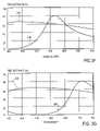
- FIG. 2Dillustrates the spectral reflectance function of this IMod design in the two states. Curves 216 and 218 reveal the reflectivity of the IMod in the white state and the black state, respectively
- FIG. 3Ais a variation that is capable of three states.
- the thin film stack of the design in FIG. 2Ahas been broken into separate movable membranes.
- Membrane 300is a metal, 400 nm of aluminum in this case, and membrane 302 is also a metal, 14 nm of tungsten for example. Because the tungsten is so thin, optically neutral structural films may be required to provide the requisite mechanical integrity, which could be in the form of a supporting frame. The air gap between the two membranes functions as the dielectric.
- FIG. 3Bshows a top view of this IMod revealing detail of how actuation would occur.
- conducting membrane 302shields membrane 300 from the electric fields produced by the stiction/actuation bumps. Lengthening membrane 300 at regions 303 , 304 so that it extends beyond the footprint of membrane 302 allows membrane 300 to “see” the electric fields via paths 305 , 307 and thus be acted upon by them.
- FIG. 3CThe three possible mechanical states, and associated dimensions, are illustrated in FIG. 3C .
- Airgap dimensions 308 and 310could be 215 nm and 135 nm.
- FIG. 3Dreveals detail of the thin films involved.
- Film 320is a metal
- 322is an airgap which serves as a dielectric
- 324is also a metal
- 326is a dielectric.
- FIG. 3Eis a spectral reflectance plot of the three states. For the dimensions indicated, a black state (e.g. state 2 ) , a blue state (state 0 ), and a white state (state 1 ) are possible, with the black, blue and white states corresponding to spectral reflectance plots, 334 , 332 , and 330 .
- FIG. 3Fshows plots for an IMod with green and white states 336 and 334
- FIG. 3Gshows plots for an IMod with red and white states 340 and 338 .
- this designexhibits electromechanical hysteresis, though it is more complicated than an IMod with only two states. There is a minimum voltage which, when applied, is sufficient to keep one or both membranes in a driven or actuated state despite the mechanical forces which seek to return them to their relaxed positions.
- FIG. 4Ais a representative plot showing the relationship between applied voltage and the state of the IMod.
- a minimum bias, Vbiasis required to maintain the IMod in the state into which it has been driven.
- State 1 and State 2are achieved by the application of voltages V 3 and V 4 .
- the related hysteresis diagramis shown in FIG. 4B , with curve 400 corresponding to the electromechanical response of movable plate 302 of FIG. 3A , and curve 402 corresponding to that of movable plate 300 .
- Vbiasresides at the average of the centers of the two curves.
- FIG. 4Cillustrates one part of a drive circuit required to actuate such a device.
- Output stage 406consists of three transistors or other suitable switches that are connected in parallel to three different voltage sources, and the two movable plates of the IMod.
- Driver logic 404responds to input signals 408 in a way that allows for the selection, via the output stage, of one particular voltage to be applied to the movable membranes of IMod 410 . When no voltage is applied, the IMod's membranes move to their relaxed state via mechanical forces.
- FIGS. 5A-5CAnother issue that can be encountered in movable membrane structures is that of charge deposition, a phenomenon illustrated in FIGS. 5A-5C .
- a voltageis applied between movable plate 500 and fixed plate 504 .
- Layer 502is an insulating film that resides on top of fixed plate 504 . If the applied voltage is sufficient to actuate the movable plate and it comes into contact with the. insulator, as it does in FIG. 5B , it may deposit charge 506 on the insulator.
- the attractive force between plates 500 and 504is reduced, and a higher voltage must be applied in order to achieve actuation ( FIG. 5C ).
- FIG. 5Dillustrates the effect of applying a reverse polarity.
- the other alternativeis to eliminate the solid insulator and replace it with air.
- FIG. 5Eillustrates the use of stiction bumps or actuation rails to accomplish this goal. Charge may still accumulate on these structures, but the area is much smaller, and therefore the accumulated charge is decreased. Reverse polarity and stiction bumps may also be used together.
- Tether 600 on IMod 602is fabricated so that it is thinner than tether 604 on IMod 606 .
- IMod 602is displaced further than IMod 606 because of its lower spring constant.
- Less forceis required to actuate this structure and its mechanical response time is lower, and it is the mechanical response time that tends to dominate.
- the same techniqueapplies to the double clamped design only the thickness of the entire membrane, or major parts of it, are varied.
- an IMod that is red and therefore has a longer mechanical response time because of the greater undriven spacingcan be fabricated with a higher spring constant. This makes it possible to match its actuation time to that of, say, the blue IMod.
- the spring constantcould be determined by lengths of the tether arms. A longer tether results in a lower spring constant and a shorter tether produces a higher constant. This could be accomplished, in the same amount of total device space, by varying the position along the edge of the movable membrane to which the tether is attached. Thus, a tether connected to the center of the membrane edge would have a lower (a higher) than one connected to the nearer (the farther) end, respectively.
- FIG. 7Areveals more detail about one possible approach.
- the movable membrane, 700is selected purely on the basis of it optical properties and membrane tether, 702 , for its advantageous mechanical properties.
- Aluminumfor example, has already been shown to be useful in several IMod designs from an optical perspective, though mechanically it is subject to fatigue and stress fractures.
- a more suitable materialmight be a dielectric like aluminum oxide, silicon oxide or silicon nitride, which could be used to construct the tether.
- FIG. 7Billustrates a variation on the theme where the tether is composed of either a laminated or graded material.
- layers 706 and 710might comprise films of aluminum oxide, providing good mechanical strength, and film 708 could be aluminum, providing electrical conductivity.
- layers 710 - 706could be composed of a continuously varied material that is deposited so that at the inner surface it is pure aluminum, and at the outer surface it is pure aluminum oxide. This approach should be mechanically more robust than the laminate. Other manifestations of this technique are possible, including the use of different materials as well as alternate material variations.
- etch chemistry of particular interestutilizes a gas-phase etchant to remove the sacrificial layer.
- Candidatesinclude gases known as XeF2, BrF3, ClF3, BrF5, and IF5. These gases have the advantageous property of etching materials such as silicon and tungsten spontaneously, and without the need for a plasma to activate the etch process. Because it is a gas phase etch, as opposed to a wet etch, the sacrificial etch step is much less complicated and provides additional flexibility in the kinds of structural materials which may be used. Furthermore it facilitates the fabrication of more elaborate devices with complex internal structures.
- Display applicationsin general, require the ability to fabricate on relatively large substrates. While many finished display devices can be smaller than 1 square inch, most direct view displays start at several square inches and can be as large as several hundred square inches or larger. Additionally, these displays utilize glass or plastic substrates that are not found in traditional semiconductor manufacturing plants. MEMS, which are primarily both silicon based and fabricated on silicon substrates, have been historically fabricated in semiconductor type facilities. However the need to fabricate large arrays of MEM devices on large substrates, a need which is exemplified by an IMod based display, cannot be served using traditional semiconductor manufacturing practices or facilities.
- the substrate of choiceis glass or plastic, which is readily available in large sized formats.
- key materials depositedinclude silicon, tungsten, molybdenum, and tantalum, all of which are suitable sacrificial materials for gas phase etchants, as well as tantalum pentoxide, silicon dioxide, silicon nitride, and aluminum, which are suitable optical, insulating, structural, optical, and conducting materials.
- all photolithography, process tooling, and testingare oriented towards large arrays and large area devices.
- the process for fabricating the TFTscan be utilized to fabricate electronics in conjunction with the MEM devices in order to provide driver circuitry and intelligent logic functions.
- Active Matrix LCD fabs and their associated processesprovide a readily usable manufacturing vehicle for IMod based displays in particular, and large area (at least as large of 14′′ ⁇ 16′′) MEM devices in general.
- TFTs and IMods or other MEM devicesTwo general approaches for fabricating TFTs and IMods or other MEM devices can be described as decoupled and overlapping. In the former the requisite TFT based circuitry is fabricated first, and then the IMods are fabricated subsequently. A more efficient approach is to fabricate the TFT array and the IMod array in a way that allows the sharing or overlapping of steps in each process.
- a representative TFT process sequenceis shown in the following:
- steps 1-6are functional equivalents on a fundamental level and, obviously, located at the same place in their respective sequences.
- This similaritybenefits both the decoupled and overlapping processes in several ways.
- the process and facilities for manufacturing the active matrix component of the AMLCDwould appear to be ideally suited for IMod fabrication.
- any thin film, medium, or substrate(which can be considered a thick film) can be defined in terms of a characteristic optical admittance.
- the operation of a thin filmcan be studied by treating it as an admittance transformer. That is, a think film or combination of thin films (the transformer) can alter the characteristic admittance of another thin film or substrate (the transformed film) upon which it is deposited. In this fashion a normally reflective film or substrate may have it's characteristic admittance altered (i.e., transformed) in such a way that its reflectivity is enhanced and/or degraded by the deposition of, or contact with, a transformer. In general there is always reflection at the interface between any combination of films, mediums, or substrates. The closer the admittance of the two, the lower the reflectance at the interface, to the point where the reflectance is zero when the admittances are matched.
- reflector 800(the transformed film) is separated from induced absorber 805 (the transformer), comprising films 804 , 806 , and 808 , by variable thickness spacer 802 .
- Incident medium 810bounds the other side of induced absorber 805 .
- Each of these thin filmsis micromachined in a fashion described in the parent patent application.
- Induced absorber 805performs two functions. The first is to match the admittances of reflector 800 and incident medium 810 . This is accomplished via matching layer 808 , which is used to transform the admittance of absorber 806 to that of the incident medium 810 , and via matching layer 804 , which is used to transform the admittance of reflector 800 to that of absorber 806 .
- the second functionis the absorption of light. This is accomplished using absorber 806 , which performs the function of attenuating light which is incident upon it through the medium, as well as light which is incident upon it from the reflector.
- pixel 900is shown in the driven state and pixel 902 in the undriven state.
- induced absorber 906the transformer
- reflector 908the transformed film
- Application of a voltagecauses reflector 908 to come into contact or close proximity with induced absorber 906 .
- Proper selection of materials and thicknesswill result in a complete transformation of the admittance of reflector 908 to that of substrate 904 . Consequently, a range of frequencies of light 905 , which is incident through substrate 904 , will be significantly absorbed by the pixel.
- reflector 908With no voltage applied, reflector 908 returns to its normal structural state which changes the relative admittances of the reflector and the substrate. In this state (pixel 902 ) the cavity behaves more like a resonant reflector, strongly reflecting certain frequencies while strongly absorbing others.
- substrate 1002is glass
- matching layer 1004is a film of zirconium dioxide which is 54.46 nm thick
- absorber 1006is a tungsten film 14.49 nm thick
- matching layer 1008is a film of silicon dioxide 50 nm thick
- spacer 1000is air
- reflector 1010is a film of silver at least 50 nm thick.
- the optical response of the pixelis shown in the driven state, i.e., when reflector 1010 is in contact with matching layer 1008 resulting in a broad state of induced absorption.
- the different color pixelsare shown in respective undriven states which correspond to the reflection of blue, green, red, and white light, respectively. These responses correspond to undriven spacer thicknesses of 325, 435, 230, and 700 nm, respectively.
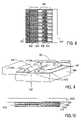
- a section of full color reflective flat panel display 1600includes three kinds of pixels, R, G, and B. Each kind differs from the others only in the size of the undriven spacer which is determined during manufacture as described in the parent patent application.
- Induced absorber 1602resides on substrate 1606 , and reflector 1610 is self-supporting.
- Monolithic backplate 1604provides a hermitic seal and can consist a thick organic or inorganic film. Alternatively, the backplate may consist of a separate piece, such as glass, which has been aligned and bonded to the substrate. Electrodes may reside on this backplate so that the electromechanical performance of the pixels may be modified.
- Incident light 1612is transmitted through optical compensation mechanism 1608 and substrate 1606 where it is selectively reflected or absorbed by a pixel.
- the displaymay be controlled and driven by circuitry of the kind described in the parent patent application.
- Optical compensation mechanism 1608serves two functions in this display. The first is that of mitigating or eliminating the shift in reflected color with respect to the angle of incidence. This is a characteristic of all interference films and can be compensated for by using films with specifically tailored refractive indices or holographic properties, as well as films containing micro-optics; other ways may also be possible.
- the second functionis to supply a supplemental frontlighting source. In this way, additional light can be added to the front of the display when ambient lighting conditions have significantly diminished thus allowing the display to perform in conditions ranging from intense brightness to total darkness.
- Such a frontlightcould be fabricated using patterned organic emitters or edge lighting source coupled to a micro-optic array within the optical compensation film; other ways may also be possible.
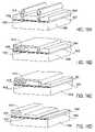
- Both alternative processesinvolve the iterative deposition and patterning of a sacrificial spacer material which, in the final step of the larger process is, etched away to form an air-gap.
- the stencil along with the excess spacer materialhave been lifted off by immersing the device in a bath of solvent such as acetone and agitating it with ultrasound.
- the processhas begun again with new photoresist 1710 having been deposited patterned in a fashion such that new spacer 1712 is deposited adjacent to the old spacer 1706 . Repeating the process once more results in spacers with three different thicknesses.
- the processhas begun again with new photoresist 1710 having been deposited patterned in a fashion such that new spacer 1712 , with a different thickness, is deposited adjacent to the old spacer 1706 .
- substrate 1800is shown with induced absorber 1802 already deposited.
- Spacer materials 1804 , 1806 , and 1808have also been deposited and patterned by virtue of lift-off stencil 1810 .
- the spacer materialshave a thickness corresponding to the maximum of the three thicknesses required for the pixels.
- FIG. 18Bthe stencil along with the excess material has been lifted off and new photoresist 1812 has been deposited and patterned such that spacer 1804 has been left exposed.
- spacer material 1804has been etched back via one of a number of techniques which include wet chemical etching, and reactive ion etching.
- Photoresist 1812is subsequently removed using a similar technique. Referring to FIG. 18D , new photoresist 1814 has been deposited and patterned exposing spacers 1804 and 1806 . The entire etch of spacer 1806 is performed in this step, and the etch of spacer 1804 is completed. Photoresist 1814 is subsequently removed and the process is complete.
- the spacer materialneed not ultimately be etched away but may remain instead a part of the finished device.
- arbitrary patternsmay be fabricated instead of arrays of simple pixels.
- Full color static graphical imagesmay thus be rendered in a method which is analogous to a conventional printing process.
- conventional printingan image is broken up into color separations which are basically monochrome graphical subsets of the image, which correspond to the different colors represented, i.e., a red separation, a blue separation, a green separation, and a black separation.
- the full-color imageis produced by printing each separation using a different colored ink on the same area.
- the different separationsare composed of layers of thin films which correspond to the IMod design described here and those in the referenced patent. Patterning or printing a combination of colors or separations on the same area, allows for brilliant full-color images to be produced.
- a square substrateis shown with area 1900 representing the portion of the substrate which has been patterned with a thin film stack optimized for black.
- the substratehas been subsequently patterned with a thin film stack optimized for red in area 1902 .
- the substratehas been subsequently patterned with a thin film stack optimized for green in area 1904 .
- the substratehas been subsequently patterned with a think film stack optimized for blue in area 1906 .
- a simpler processcan be obtained if only the induced absorber design is used.
- the entire substrateis first coated with the induced absorber stack.
- Subsequent stepsare then used to pattern the spacer material only, using the aforementioned techniques.
- a final deposition of a reflectoris performed.
- the brightness of different colorscan be altered by varying the amount of black interspersed with the particular color, i.e., spatial dithering.
- the imagesalso exhibit the pleasing shift of color with respect to viewing angle known as iridescence.
- a reflective flat panel displaymay also be fabricated using a single kind of pixel instead of three. Multiple colors, in this case, are obtained through fabricating the pixels in the form of continuously tunable or analog interferometric modulators as described in the parent patent application. In this fashion, any individual pixel may, by the application of the appropriate voltage, be tuned to reflect any specific color. This would require that the array be fabricated on a substrate along with electronic circuitry, or directly on the surface of an integrated circuit, in order to provide a charge storage mechanism. This approach, though it requires a more complicated driving scheme relying on analog voltages, provides superior resolution. It would also find application in a projection system.
Landscapes
- Physics & Mathematics (AREA)
- General Physics & Mathematics (AREA)
- Optics & Photonics (AREA)
- Engineering & Computer Science (AREA)
- Nonlinear Science (AREA)
- Theoretical Computer Science (AREA)
- Computer Hardware Design (AREA)
- Chemical & Material Sciences (AREA)
- Spectroscopy & Molecular Physics (AREA)
- Crystallography & Structural Chemistry (AREA)
- Nanotechnology (AREA)
- Life Sciences & Earth Sciences (AREA)
- Biophysics (AREA)
- Microelectronics & Electronic Packaging (AREA)
- Electromagnetism (AREA)
- Mechanical Light Control Or Optical Switches (AREA)
- Control Of Indicators Other Than Cathode Ray Tubes (AREA)
Abstract
Description
Claims (17)
Priority Applications (5)
| Application Number | Priority Date | Filing Date | Title |
|---|---|---|---|
| US10/752,140US7692844B2 (en) | 1994-05-05 | 2004-01-05 | Interferometric modulation of radiation |
| US11/492,535US7554711B2 (en) | 1998-04-08 | 2006-07-24 | MEMS devices with stiction bumps |
| US12/031,603US8105496B2 (en) | 1994-05-05 | 2008-02-14 | Method of fabricating MEMS devices (such as IMod) comprising using a gas phase etchant to remove a layer |
| US13/333,257US20120085731A1 (en) | 1998-04-08 | 2011-12-21 | METHOD OF FABRICATING MEMS DEVICES (SUCH AS IMod) COMPRISING USING A GAS PHASE ETCHANT TO REMOVE A LAYER |
| US13/333,208US20120099174A1 (en) | 1998-04-08 | 2011-12-21 | METHOD OF FABRICATING MEMS DEVICES (SUCH AS IMod) COMPRISING USING A GAS PHASE ETCHANT TO REMOVE A LAYER |
Applications Claiming Priority (6)
| Application Number | Priority Date | Filing Date | Title |
|---|---|---|---|
| US08/238,750US5835255A (en) | 1986-04-23 | 1994-05-05 | Visible spectrum modulator arrays |
| US55463095A | 1995-11-06 | 1995-11-06 | |
| US76994796A | 1996-12-19 | 1996-12-19 | |
| US09/056,975US6674562B1 (en) | 1994-05-05 | 1998-04-08 | Interferometric modulation of radiation |
| US09/966,843US6867896B2 (en) | 1994-05-05 | 2001-09-28 | Interferometric modulation of radiation |
| US10/752,140US7692844B2 (en) | 1994-05-05 | 2004-01-05 | Interferometric modulation of radiation |
Related Parent Applications (1)
| Application Number | Title | Priority Date | Filing Date |
|---|---|---|---|
| US09/966,843DivisionUS6867896B2 (en) | 1993-03-17 | 2001-09-28 | Interferometric modulation of radiation |
Related Child Applications (2)
| Application Number | Title | Priority Date | Filing Date |
|---|---|---|---|
| US11/492,535ContinuationUS7554711B2 (en) | 1998-04-08 | 2006-07-24 | MEMS devices with stiction bumps |
| US12/031,603DivisionUS8105496B2 (en) | 1994-05-05 | 2008-02-14 | Method of fabricating MEMS devices (such as IMod) comprising using a gas phase etchant to remove a layer |
Publications (2)
| Publication Number | Publication Date |
|---|---|
| US20040240032A1 US20040240032A1 (en) | 2004-12-02 |
| US7692844B2true US7692844B2 (en) | 2010-04-06 |
Family
ID=27489850
Family Applications (14)
| Application Number | Title | Priority Date | Filing Date |
|---|---|---|---|
| US09/056,975Expired - Fee RelatedUS6674562B1 (en) | 1993-03-17 | 1998-04-08 | Interferometric modulation of radiation |
| US09/966,843Expired - Fee RelatedUS6867896B2 (en) | 1993-03-17 | 2001-09-28 | Interferometric modulation of radiation |
| US10/752,140Expired - Fee RelatedUS7692844B2 (en) | 1994-05-05 | 2004-01-05 | Interferometric modulation of radiation |
| US11/056,571Expired - Fee RelatedUS7379227B2 (en) | 1993-03-17 | 2005-02-11 | Method and device for modulating light |
| US11/070,497Expired - Fee RelatedUS7012732B2 (en) | 1994-05-05 | 2005-03-01 | Method and device for modulating light with a time-varying signal |
| US11/192,436Expired - Fee RelatedUS7463421B2 (en) | 1994-05-05 | 2005-07-28 | Method and device for modulating light |
| US11/432,724Expired - Fee RelatedUS7848001B2 (en) | 1994-05-05 | 2006-05-11 | Method and system for interferometric modulation in projection or peripheral devices |
| US11/626,792Expired - Fee RelatedUS8284474B2 (en) | 1994-05-05 | 2007-01-24 | Method and system for interferometric modulation in projection or peripheral devices |
| US11/668,973Expired - Fee RelatedUS7846344B2 (en) | 1994-05-05 | 2007-01-30 | Method and device for modulating light |
| US11/742,271Expired - Fee RelatedUS8059326B2 (en) | 1994-05-05 | 2007-04-30 | Display devices comprising of interferometric modulator and sensor |
| US11/754,229Expired - Fee RelatedUS7532381B2 (en) | 1994-05-05 | 2007-05-25 | Method of making a light modulating display device and associated transistor circuitry and structures thereof |
| US11/841,847Expired - Fee RelatedUS7848004B2 (en) | 1994-05-05 | 2007-08-20 | System and method for a MEMS device |
| US12/031,603Expired - Fee RelatedUS8105496B2 (en) | 1994-05-05 | 2008-02-14 | Method of fabricating MEMS devices (such as IMod) comprising using a gas phase etchant to remove a layer |
| US12/815,136Expired - Fee RelatedUS8054532B2 (en) | 1994-05-05 | 2010-06-14 | Method and device for providing illumination to interferometric modulators |
Family Applications Before (2)
| Application Number | Title | Priority Date | Filing Date |
|---|---|---|---|
| US09/056,975Expired - Fee RelatedUS6674562B1 (en) | 1993-03-17 | 1998-04-08 | Interferometric modulation of radiation |
| US09/966,843Expired - Fee RelatedUS6867896B2 (en) | 1993-03-17 | 2001-09-28 | Interferometric modulation of radiation |
Family Applications After (11)
| Application Number | Title | Priority Date | Filing Date |
|---|---|---|---|
| US11/056,571Expired - Fee RelatedUS7379227B2 (en) | 1993-03-17 | 2005-02-11 | Method and device for modulating light |
| US11/070,497Expired - Fee RelatedUS7012732B2 (en) | 1994-05-05 | 2005-03-01 | Method and device for modulating light with a time-varying signal |
| US11/192,436Expired - Fee RelatedUS7463421B2 (en) | 1994-05-05 | 2005-07-28 | Method and device for modulating light |
| US11/432,724Expired - Fee RelatedUS7848001B2 (en) | 1994-05-05 | 2006-05-11 | Method and system for interferometric modulation in projection or peripheral devices |
| US11/626,792Expired - Fee RelatedUS8284474B2 (en) | 1994-05-05 | 2007-01-24 | Method and system for interferometric modulation in projection or peripheral devices |
| US11/668,973Expired - Fee RelatedUS7846344B2 (en) | 1994-05-05 | 2007-01-30 | Method and device for modulating light |
| US11/742,271Expired - Fee RelatedUS8059326B2 (en) | 1994-05-05 | 2007-04-30 | Display devices comprising of interferometric modulator and sensor |
| US11/754,229Expired - Fee RelatedUS7532381B2 (en) | 1994-05-05 | 2007-05-25 | Method of making a light modulating display device and associated transistor circuitry and structures thereof |
| US11/841,847Expired - Fee RelatedUS7848004B2 (en) | 1994-05-05 | 2007-08-20 | System and method for a MEMS device |
| US12/031,603Expired - Fee RelatedUS8105496B2 (en) | 1994-05-05 | 2008-02-14 | Method of fabricating MEMS devices (such as IMod) comprising using a gas phase etchant to remove a layer |
| US12/815,136Expired - Fee RelatedUS8054532B2 (en) | 1994-05-05 | 2010-06-14 | Method and device for providing illumination to interferometric modulators |
Country Status (1)
| Country | Link |
|---|---|
| US (14) | US6674562B1 (en) |
Cited By (37)
| Publication number | Priority date | Publication date | Assignee | Title |
|---|---|---|---|---|
| US20100214645A1 (en)* | 1996-12-19 | 2010-08-26 | Qualcomm Mems Technologies, Inc. | Separable modulator |
| US20100290102A1 (en)* | 2008-07-17 | 2010-11-18 | Qualcomm Mems Technologies, Inc. | Encapsulated electromechanical devices |
| US20110080632A1 (en)* | 1996-12-19 | 2011-04-07 | Qualcomm Mems Technologies, Inc. | Method of making a light modulating display device and associated transistor circuitry and structures thereof |
| US20110170167A1 (en)* | 1998-04-08 | 2011-07-14 | Qualcomm Mems Technologies, Inc. | Method for modulating light with multiple electrodes |
| US20110170168A1 (en)* | 2007-07-02 | 2011-07-14 | Qualcomm Mems Technologies, Inc. | Electromechanical device with optical function separated from mechanical and electrical function |
| US20110188110A1 (en)* | 1995-05-01 | 2011-08-04 | Miles Mark W | Microelectromechanical device with restoring electrode |
| US8035883B2 (en) | 2004-09-27 | 2011-10-11 | Qualcomm Mems Technologies, Inc. | Device having a conductive light absorbing mask and method for fabricating same |
| WO2011130718A2 (en) | 2010-04-16 | 2011-10-20 | Flex Lighting Ii, Llc | Front illumination device comprising a film-based lightguide |
| WO2011130715A2 (en) | 2010-04-16 | 2011-10-20 | Flex Lighting Ii, Llc | Illumination device comprising a film-based lightguide |
| US8058549B2 (en) | 2007-10-19 | 2011-11-15 | Qualcomm Mems Technologies, Inc. | Photovoltaic devices with integrated color interferometric film stacks |
| US8081373B2 (en) | 2007-07-31 | 2011-12-20 | Qualcomm Mems Technologies, Inc. | Devices and methods for enhancing color shift of interferometric modulators |
| US8098417B2 (en) | 2007-05-09 | 2012-01-17 | Qualcomm Mems Technologies, Inc. | Electromechanical system having a dielectric movable membrane |
| US8213075B2 (en) | 2004-09-27 | 2012-07-03 | Qualcomm Mems Technologies, Inc. | Method and device for multistate interferometric light modulation |
| US8358266B2 (en) | 2008-09-02 | 2013-01-22 | Qualcomm Mems Technologies, Inc. | Light turning device with prismatic light turning features |
| US8390547B2 (en) | 2004-09-27 | 2013-03-05 | Qualcomm Mems Technologies, Inc. | Conductive bus structure for interferometric modulator array |
| US8488228B2 (en) | 2009-09-28 | 2013-07-16 | Qualcomm Mems Technologies, Inc. | Interferometric display with interferometric reflector |
| US8659816B2 (en) | 2011-04-25 | 2014-02-25 | Qualcomm Mems Technologies, Inc. | Mechanical layer and methods of making the same |
| US8693084B2 (en) | 2008-03-07 | 2014-04-08 | Qualcomm Mems Technologies, Inc. | Interferometric modulator in transmission mode |
| US8736939B2 (en) | 2011-11-04 | 2014-05-27 | Qualcomm Mems Technologies, Inc. | Matching layer thin-films for an electromechanical systems reflective display device |
| US8798425B2 (en) | 2007-12-07 | 2014-08-05 | Qualcomm Mems Technologies, Inc. | Decoupled holographic film and diffuser |
| US8797632B2 (en) | 2010-08-17 | 2014-08-05 | Qualcomm Mems Technologies, Inc. | Actuation and calibration of charge neutral electrode of a display device |
| US8797628B2 (en) | 2007-10-19 | 2014-08-05 | Qualcomm Memstechnologies, Inc. | Display with integrated photovoltaic device |
| US8817357B2 (en) | 2010-04-09 | 2014-08-26 | Qualcomm Mems Technologies, Inc. | Mechanical layer and methods of forming the same |
| US8861071B2 (en) | 2004-09-27 | 2014-10-14 | Qualcomm Mems Technologies, Inc. | Method and device for compensating for color shift as a function of angle of view |
| US8872085B2 (en) | 2006-10-06 | 2014-10-28 | Qualcomm Mems Technologies, Inc. | Display device having front illuminator with turning features |
| US8885244B2 (en) | 2004-09-27 | 2014-11-11 | Qualcomm Mems Technologies, Inc. | Display device |
| US8928967B2 (en) | 1998-04-08 | 2015-01-06 | Qualcomm Mems Technologies, Inc. | Method and device for modulating light |
| US8941631B2 (en) | 2007-11-16 | 2015-01-27 | Qualcomm Mems Technologies, Inc. | Simultaneous light collection and illumination on an active display |
| US8963159B2 (en) | 2011-04-04 | 2015-02-24 | Qualcomm Mems Technologies, Inc. | Pixel via and methods of forming the same |
| US8971675B2 (en) | 2006-01-13 | 2015-03-03 | Qualcomm Mems Technologies, Inc. | Interconnect structure for MEMS device |
| US8979349B2 (en) | 2009-05-29 | 2015-03-17 | Qualcomm Mems Technologies, Inc. | Illumination devices and methods of fabrication thereof |
| US9001412B2 (en) | 2004-09-27 | 2015-04-07 | Qualcomm Mems Technologies, Inc. | Electromechanical device with optical function separated from mechanical and electrical function |
| US9019183B2 (en) | 2006-10-06 | 2015-04-28 | Qualcomm Mems Technologies, Inc. | Optical loss structure integrated in an illumination apparatus |
| US9019590B2 (en) | 2004-02-03 | 2015-04-28 | Qualcomm Mems Technologies, Inc. | Spatial light modulator with integrated optical compensation structure |
| US9025235B2 (en) | 2002-12-25 | 2015-05-05 | Qualcomm Mems Technologies, Inc. | Optical interference type of color display having optical diffusion layer between substrate and electrode |
| US9057872B2 (en) | 2010-08-31 | 2015-06-16 | Qualcomm Mems Technologies, Inc. | Dielectric enhanced mirror for IMOD display |
| US9134527B2 (en) | 2011-04-04 | 2015-09-15 | Qualcomm Mems Technologies, Inc. | Pixel via and methods of forming the same |
Families Citing this family (649)
| Publication number | Priority date | Publication date | Assignee | Title |
|---|---|---|---|---|
| US5877897A (en) | 1993-02-26 | 1999-03-02 | Donnelly Corporation | Automatic rearview mirror, vehicle lighting control and vehicle interior monitoring system using a photosensor array |
| US6822563B2 (en) | 1997-09-22 | 2004-11-23 | Donnelly Corporation | Vehicle imaging system with accessory control |
| US6674562B1 (en)* | 1994-05-05 | 2004-01-06 | Iridigm Display Corporation | Interferometric modulation of radiation |
| US7138984B1 (en) | 2001-06-05 | 2006-11-21 | Idc, Llc | Directly laminated touch sensitive screen |
| US20010003487A1 (en)* | 1996-11-05 | 2001-06-14 | Mark W. Miles | Visible spectrum modulator arrays |
| US7550794B2 (en)* | 2002-09-20 | 2009-06-23 | Idc, Llc | Micromechanical systems device comprising a displaceable electrode and a charge-trapping layer |
| US7808694B2 (en)* | 1994-05-05 | 2010-10-05 | Qualcomm Mems Technologies, Inc. | Method and device for modulating light |
| US7800809B2 (en) | 1994-05-05 | 2010-09-21 | Qualcomm Mems Technologies, Inc. | System and method for a MEMS device |
| US7776631B2 (en) | 1994-05-05 | 2010-08-17 | Qualcomm Mems Technologies, Inc. | MEMS device and method of forming a MEMS device |
| US6680792B2 (en)* | 1994-05-05 | 2004-01-20 | Iridigm Display Corporation | Interferometric modulation of radiation |
| US7297471B1 (en) | 2003-04-15 | 2007-11-20 | Idc, Llc | Method for manufacturing an array of interferometric modulators |
| US7123216B1 (en)* | 1994-05-05 | 2006-10-17 | Idc, Llc | Photonic MEMS and structures |
| US7839556B2 (en)* | 1994-05-05 | 2010-11-23 | Qualcomm Mems Technologies, Inc. | Method and device for modulating light |
| US7852545B2 (en) | 1994-05-05 | 2010-12-14 | Qualcomm Mems Technologies, Inc. | Method and device for modulating light |
| US8014059B2 (en)* | 1994-05-05 | 2011-09-06 | Qualcomm Mems Technologies, Inc. | System and method for charge control in a MEMS device |
| US6891563B2 (en) | 1996-05-22 | 2005-05-10 | Donnelly Corporation | Vehicular vision system |
| US7907319B2 (en)* | 1995-11-06 | 2011-03-15 | Qualcomm Mems Technologies, Inc. | Method and device for modulating light with optical compensation |
| US7655894B2 (en) | 1996-03-25 | 2010-02-02 | Donnelly Corporation | Vehicular image sensing system |
| US7929197B2 (en)* | 1996-11-05 | 2011-04-19 | Qualcomm Mems Technologies, Inc. | System and method for a MEMS device |
| US7471444B2 (en)* | 1996-12-19 | 2008-12-30 | Idc, Llc | Interferometric modulation of radiation |
| US7532377B2 (en) | 1998-04-08 | 2009-05-12 | Idc, Llc | Movable micro-electromechanical device |
| US6180426B1 (en) | 1999-03-01 | 2001-01-30 | Mou-Shiung Lin | High performance sub-system design and assembly |
| US8023724B2 (en)* | 1999-07-22 | 2011-09-20 | Photon-X, Inc. | Apparatus and method of information extraction from electromagnetic energy based upon multi-characteristic spatial geometry processing |
| WO2003007049A1 (en) | 1999-10-05 | 2003-01-23 | Iridigm Display Corporation | Photonic mems and structures |
| US6960305B2 (en)* | 1999-10-26 | 2005-11-01 | Reflectivity, Inc | Methods for forming and releasing microelectromechanical structures |
| US7167796B2 (en)* | 2000-03-09 | 2007-01-23 | Donnelly Corporation | Vehicle navigation system for use with a telematics system |
| US6504643B1 (en)* | 2000-09-28 | 2003-01-07 | Xerox Corporation | Structure for an optical switch on a substrate |
| US6466356B1 (en)* | 2000-09-28 | 2002-10-15 | Xerox Corporation | Structure for an optical switch on a silicon substrate |
| US6501588B1 (en)* | 2000-09-28 | 2002-12-31 | Xerox Corporation | Method for an optical switch on a silicon substrate |
| US6859577B2 (en)* | 2001-06-25 | 2005-02-22 | Analog Devices Inc. | Self assembled micro anti-stiction structure |
| TWI313507B (en) | 2002-10-25 | 2009-08-11 | Megica Corporatio | Method for assembling chips |
| US6515791B1 (en)* | 2001-04-06 | 2003-02-04 | Read-Rite Corporation | Active reflection and anti-reflection optical switch |
| KR100452112B1 (en)* | 2001-07-18 | 2004-10-12 | 한국과학기술원 | Electrostatic Actuator |
| US6882287B2 (en) | 2001-07-31 | 2005-04-19 | Donnelly Corporation | Automotive lane change aid |
| US7697027B2 (en) | 2001-07-31 | 2010-04-13 | Donnelly Corporation | Vehicular video system |
| US6589625B1 (en)* | 2001-08-01 | 2003-07-08 | Iridigm Display Corporation | Hermetic seal and method to create the same |
| CA2495722A1 (en)* | 2001-08-17 | 2003-02-27 | Cae Inc. | Video projector and optical light valve therefor |
| US6847483B2 (en)* | 2001-12-21 | 2005-01-25 | Bose Corporation | Selective reflecting |
| US20050231800A1 (en)* | 2001-12-21 | 2005-10-20 | Barret Lippey | Selective reflecting |
| US7520624B2 (en)* | 2001-12-21 | 2009-04-21 | Bose Corporation | Light enhancing |
| US7515336B2 (en)* | 2001-12-21 | 2009-04-07 | Bose Corporation | Selective reflecting |
| TW544882B (en) | 2001-12-31 | 2003-08-01 | Megic Corp | Chip package structure and process thereof |
| TW584950B (en) | 2001-12-31 | 2004-04-21 | Megic Corp | Chip packaging structure and process thereof |
| US6673698B1 (en) | 2002-01-19 | 2004-01-06 | Megic Corporation | Thin film semiconductor package utilizing a glass substrate with composite polymer/metal interconnect layers |
| TW503496B (en) | 2001-12-31 | 2002-09-21 | Megic Corp | Chip packaging structure and manufacturing process of the same |
| JP3818372B2 (en)* | 2002-01-11 | 2006-09-06 | セイコーエプソン株式会社 | Printing apparatus, printing control program, medium recording printing control program, and printing method |
| US6794119B2 (en)* | 2002-02-12 | 2004-09-21 | Iridigm Display Corporation | Method for fabricating a structure for a microelectromechanical systems (MEMS) device |
| US6574033B1 (en)* | 2002-02-27 | 2003-06-03 | Iridigm Display Corporation | Microelectromechanical systems device and method for fabricating same |
| CN100387749C (en)* | 2002-04-15 | 2008-05-14 | 肖特股份公司 | Method for forming housings for electronic components and sealing packaged electronic components by such method |
| ES2391556T3 (en) | 2002-05-03 | 2012-11-27 | Donnelly Corporation | Object detection system for vehicles |
| US20040212026A1 (en)* | 2002-05-07 | 2004-10-28 | Hewlett-Packard Company | MEMS device having time-varying control |
| US7781850B2 (en)* | 2002-09-20 | 2010-08-24 | Qualcomm Mems Technologies, Inc. | Controlling electromechanical behavior of structures within a microelectromechanical systems device |
| US7370185B2 (en)* | 2003-04-30 | 2008-05-06 | Hewlett-Packard Development Company, L.P. | Self-packaged optical interference display device having anti-stiction bumps, integral micro-lens, and reflection-absorbing layers |
| US7019434B2 (en) | 2002-11-08 | 2006-03-28 | Iris Ao, Inc. | Deformable mirror method and apparatus including bimorph flexures and integrated drive |
| US20040160118A1 (en) | 2002-11-08 | 2004-08-19 | Knollenberg Clifford F. | Actuator apparatus and method for improved deflection characteristics |
| WO2004054088A2 (en)* | 2002-12-10 | 2004-06-24 | Koninklijke Philips Electronics N.V. | Driving of an array of micro-electro-mechanical-system (mems) elements |
| TW200413810A (en)* | 2003-01-29 | 2004-08-01 | Prime View Int Co Ltd | Light interference display panel and its manufacturing method |
| US7417782B2 (en)* | 2005-02-23 | 2008-08-26 | Pixtronix, Incorporated | Methods and apparatus for spatial light modulation |
| JP4282346B2 (en)* | 2003-03-13 | 2009-06-17 | オリンパス株式会社 | Electrostatic drive device and manufacturing method thereof |
| US6913942B2 (en)* | 2003-03-28 | 2005-07-05 | Reflectvity, Inc | Sacrificial layers for use in fabrications of microelectromechanical devices |
| TWI226504B (en)* | 2003-04-21 | 2005-01-11 | Prime View Int Co Ltd | A structure of an interference display cell |
| TW567355B (en)* | 2003-04-21 | 2003-12-21 | Prime View Int Co Ltd | An interference display cell and fabrication method thereof |
| TW594360B (en)* | 2003-04-21 | 2004-06-21 | Prime View Int Corp Ltd | A method for fabricating an interference display cell |
| US7447891B2 (en)* | 2003-04-30 | 2008-11-04 | Hewlett-Packard Development Company, L.P. | Light modulator with concentric control-electrode structure |
| US7218438B2 (en)* | 2003-04-30 | 2007-05-15 | Hewlett-Packard Development Company, L.P. | Optical electronic device with partial reflector layer |
| US6829132B2 (en)* | 2003-04-30 | 2004-12-07 | Hewlett-Packard Development Company, L.P. | Charge control of micro-electromechanical device |
| US7072093B2 (en)* | 2003-04-30 | 2006-07-04 | Hewlett-Packard Development Company, L.P. | Optical interference pixel display with charge control |
| US6940630B2 (en)* | 2003-05-01 | 2005-09-06 | University Of Florida Research Foundation, Inc. | Vertical displacement device |
| TW570896B (en) | 2003-05-26 | 2004-01-11 | Prime View Int Co Ltd | A method for fabricating an interference display cell |
| US7221495B2 (en)* | 2003-06-24 | 2007-05-22 | Idc Llc | Thin film precursor stack for MEMS manufacturing |
| TWI251712B (en)* | 2003-08-15 | 2006-03-21 | Prime View Int Corp Ltd | Interference display plate |
| TW200506479A (en)* | 2003-08-15 | 2005-02-16 | Prime View Int Co Ltd | Color changeable pixel for an interference display |
| TW593127B (en) | 2003-08-18 | 2004-06-21 | Prime View Int Co Ltd | Interference display plate and manufacturing method thereof |
| TWI231865B (en)* | 2003-08-26 | 2005-05-01 | Prime View Int Co Ltd | An interference display cell and fabrication method thereof |
| CN100363775C (en)* | 2003-08-26 | 2008-01-23 | 高通Mems科技公司 | Light interference display panel and its mfg. method |
| JP3979982B2 (en)* | 2003-08-29 | 2007-09-19 | シャープ株式会社 | Interferometric modulator and display device |
| TWI232333B (en)* | 2003-09-03 | 2005-05-11 | Prime View Int Co Ltd | Display unit using interferometric modulation and manufacturing method thereof |
| CN100346223C (en)* | 2003-09-09 | 2007-10-31 | 高通Mems科技公司 | Reflection type interference regulating display element and method for manufacturing same |
| CN100349034C (en)* | 2003-09-09 | 2007-11-14 | 高通Mems科技公司 | Interference regulating display assembly and method for manufacturing same |
| US6982820B2 (en)* | 2003-09-26 | 2006-01-03 | Prime View International Co., Ltd. | Color changeable pixel |
| TW593126B (en)* | 2003-09-30 | 2004-06-21 | Prime View Int Co Ltd | A structure of a micro electro mechanical system and manufacturing the same |
| US20070009899A1 (en)* | 2003-10-02 | 2007-01-11 | Mounts William M | Nucleic acid arrays for detecting gene expression in animal models of inflammatory diseases |
| US7308341B2 (en) | 2003-10-14 | 2007-12-11 | Donnelly Corporation | Vehicle communication system |
| US7012726B1 (en) | 2003-11-03 | 2006-03-14 | Idc, Llc | MEMS devices with unreleased thin film components |
| US7161728B2 (en) | 2003-12-09 | 2007-01-09 | Idc, Llc | Area array modulation and lead reduction in interferometric modulators |
| US7142346B2 (en)* | 2003-12-09 | 2006-11-28 | Idc, Llc | System and method for addressing a MEMS display |
| DE10358967B4 (en)* | 2003-12-15 | 2006-11-16 | Universität Kassel | Micromirror array |
| US7532194B2 (en)* | 2004-02-03 | 2009-05-12 | Idc, Llc | Driver voltage adjuster |
| US6925781B1 (en)* | 2004-02-03 | 2005-08-09 | Playtex Products, Inc. | Integrated cutting tool for waste disposal method and apparatus |
| US7119945B2 (en)* | 2004-03-03 | 2006-10-10 | Idc, Llc | Altering temporal response of microelectromechanical elements |
| US7706050B2 (en)* | 2004-03-05 | 2010-04-27 | Qualcomm Mems Technologies, Inc. | Integrated modulator illumination |
| US7855824B2 (en)* | 2004-03-06 | 2010-12-21 | Qualcomm Mems Technologies, Inc. | Method and system for color optimization in a display |
| JP2005250376A (en)* | 2004-03-08 | 2005-09-15 | Seiko Epson Corp | Optical modulator and method for manufacturing optical modulator |
| US7227568B2 (en)* | 2004-04-03 | 2007-06-05 | Li Sun | Dual polarizing light filter for 2-D and 3-D display |
| US7526103B2 (en) | 2004-04-15 | 2009-04-28 | Donnelly Corporation | Imaging system for vehicle |
| US7476327B2 (en)* | 2004-05-04 | 2009-01-13 | Idc, Llc | Method of manufacture for microelectromechanical devices |
| US7060895B2 (en)* | 2004-05-04 | 2006-06-13 | Idc, Llc | Modifying the electro-mechanical behavior of devices |
| US7164520B2 (en) | 2004-05-12 | 2007-01-16 | Idc, Llc | Packaging for an interferometric modulator |
| US7256922B2 (en)* | 2004-07-02 | 2007-08-14 | Idc, Llc | Interferometric modulators with thin film transistors |
| TWI233916B (en)* | 2004-07-09 | 2005-06-11 | Prime View Int Co Ltd | A structure of a micro electro mechanical system |
| US7110122B2 (en)* | 2004-07-21 | 2006-09-19 | Hewlett-Packard Development Company, L.P. | Interferometer calibration methods and apparatus |
| EP2246726B1 (en)* | 2004-07-29 | 2013-04-03 | QUALCOMM MEMS Technologies, Inc. | System and method for micro-electromechanical operating of an interferometric modulator |
| US7515147B2 (en)* | 2004-08-27 | 2009-04-07 | Idc, Llc | Staggered column drive circuit systems and methods |
| US7889163B2 (en)* | 2004-08-27 | 2011-02-15 | Qualcomm Mems Technologies, Inc. | Drive method for MEMS devices |
| US7560299B2 (en)* | 2004-08-27 | 2009-07-14 | Idc, Llc | Systems and methods of actuating MEMS display elements |
| US7551159B2 (en) | 2004-08-27 | 2009-06-23 | Idc, Llc | System and method of sensing actuation and release voltages of an interferometric modulator |
| US7499208B2 (en)* | 2004-08-27 | 2009-03-03 | Udc, Llc | Current mode display driver circuit realization feature |
| US6980346B1 (en) | 2004-09-15 | 2005-12-27 | Hewlett-Packard Development Company, L.P. | Display device |
| US7602375B2 (en) | 2004-09-27 | 2009-10-13 | Idc, Llc | Method and system for writing data to MEMS display elements |
| US7345805B2 (en)* | 2004-09-27 | 2008-03-18 | Idc, Llc | Interferometric modulator array with integrated MEMS electrical switches |
| US20060065622A1 (en)* | 2004-09-27 | 2006-03-30 | Floyd Philip D | Method and system for xenon fluoride etching with enhanced efficiency |
| US7750886B2 (en)* | 2004-09-27 | 2010-07-06 | Qualcomm Mems Technologies, Inc. | Methods and devices for lighting displays |
| US8878825B2 (en)* | 2004-09-27 | 2014-11-04 | Qualcomm Mems Technologies, Inc. | System and method for providing a variable refresh rate of an interferometric modulator display |
| US7813026B2 (en) | 2004-09-27 | 2010-10-12 | Qualcomm Mems Technologies, Inc. | System and method of reducing color shift in a display |
| US7405861B2 (en)* | 2004-09-27 | 2008-07-29 | Idc, Llc | Method and device for protecting interferometric modulators from electrostatic discharge |
| US8031133B2 (en)* | 2004-09-27 | 2011-10-04 | Qualcomm Mems Technologies, Inc. | Method and device for manipulating color in a display |
| US7920135B2 (en)* | 2004-09-27 | 2011-04-05 | Qualcomm Mems Technologies, Inc. | Method and system for driving a bi-stable display |
| US7898521B2 (en)* | 2004-09-27 | 2011-03-01 | Qualcomm Mems Technologies, Inc. | Device and method for wavelength filtering |
| US20060077148A1 (en)* | 2004-09-27 | 2006-04-13 | Gally Brian J | Method and device for manipulating color in a display |
| US7675669B2 (en)* | 2004-09-27 | 2010-03-09 | Qualcomm Mems Technologies, Inc. | Method and system for driving interferometric modulators |
| US7573547B2 (en)* | 2004-09-27 | 2009-08-11 | Idc, Llc | System and method for protecting micro-structure of display array using spacers in gap within display device |
| US7349141B2 (en)* | 2004-09-27 | 2008-03-25 | Idc, Llc | Method and post structures for interferometric modulation |
| US7368803B2 (en)* | 2004-09-27 | 2008-05-06 | Idc, Llc | System and method for protecting microelectromechanical systems array using back-plate with non-flat portion |
| US8102407B2 (en)* | 2004-09-27 | 2012-01-24 | Qualcomm Mems Technologies, Inc. | Method and device for manipulating color in a display |
| US7535466B2 (en)* | 2004-09-27 | 2009-05-19 | Idc, Llc | System with server based control of client device display features |
| US7564612B2 (en)* | 2004-09-27 | 2009-07-21 | Idc, Llc | Photonic MEMS and structures |
| CN101006491A (en)* | 2004-09-27 | 2007-07-25 | Idc公司 | Measuring and modeling power consumption in displays |
| US7710636B2 (en)* | 2004-09-27 | 2010-05-04 | Qualcomm Mems Technologies, Inc. | Systems and methods using interferometric optical modulators and diffusers |
| US8514169B2 (en) | 2004-09-27 | 2013-08-20 | Qualcomm Mems Technologies, Inc. | Apparatus and system for writing data to electromechanical display elements |
| US8004504B2 (en)* | 2004-09-27 | 2011-08-23 | Qualcomm Mems Technologies, Inc. | Reduced capacitance display element |
| US7586484B2 (en)* | 2004-09-27 | 2009-09-08 | Idc, Llc | Controller and driver features for bi-stable display |
| US7136213B2 (en)* | 2004-09-27 | 2006-11-14 | Idc, Llc | Interferometric modulators having charge persistence |
| US20060076634A1 (en)* | 2004-09-27 | 2006-04-13 | Lauren Palmateer | Method and system for packaging MEMS devices with incorporated getter |
| US7527995B2 (en)* | 2004-09-27 | 2009-05-05 | Qualcomm Mems Technologies, Inc. | Method of making prestructure for MEMS systems |
| US7373026B2 (en)* | 2004-09-27 | 2008-05-13 | Idc, Llc | MEMS device fabricated on a pre-patterned substrate |
| US20060066557A1 (en)* | 2004-09-27 | 2006-03-30 | Floyd Philip D | Method and device for reflective display with time sequential color illumination |
| US7553684B2 (en)* | 2004-09-27 | 2009-06-30 | Idc, Llc | Method of fabricating interferometric devices using lift-off processing techniques |
| US7161730B2 (en) | 2004-09-27 | 2007-01-09 | Idc, Llc | System and method for providing thermal compensation for an interferometric modulator display |
| US7843410B2 (en) | 2004-09-27 | 2010-11-30 | Qualcomm Mems Technologies, Inc. | Method and device for electrically programmable display |
| US7551246B2 (en)* | 2004-09-27 | 2009-06-23 | Idc, Llc. | System and method for display device with integrated desiccant |
| US20060132383A1 (en)* | 2004-09-27 | 2006-06-22 | Idc, Llc | System and method for illuminating interferometric modulator display |
| US7554714B2 (en)* | 2004-09-27 | 2009-06-30 | Idc, Llc | Device and method for manipulation of thermal response in a modulator |
| US7317568B2 (en)* | 2004-09-27 | 2008-01-08 | Idc, Llc | System and method of implementation of interferometric modulators for display mirrors |
| US7417735B2 (en)* | 2004-09-27 | 2008-08-26 | Idc, Llc | Systems and methods for measuring color and contrast in specular reflective devices |
| US7460246B2 (en)* | 2004-09-27 | 2008-12-02 | Idc, Llc | Method and system for sensing light using interferometric elements |
| US7525730B2 (en)* | 2004-09-27 | 2009-04-28 | Idc, Llc | Method and device for generating white in an interferometric modulator display |
| US7626581B2 (en)* | 2004-09-27 | 2009-12-01 | Idc, Llc | Device and method for display memory using manipulation of mechanical response |
| US20060067650A1 (en)* | 2004-09-27 | 2006-03-30 | Clarence Chui | Method of making a reflective display device using thin film transistor production techniques |
| US7653371B2 (en)* | 2004-09-27 | 2010-01-26 | Qualcomm Mems Technologies, Inc. | Selectable capacitance circuit |
| US7911428B2 (en)* | 2004-09-27 | 2011-03-22 | Qualcomm Mems Technologies, Inc. | Method and device for manipulating color in a display |
| US20060066594A1 (en)* | 2004-09-27 | 2006-03-30 | Karen Tyger | Systems and methods for driving a bi-stable display element |
| US7724993B2 (en) | 2004-09-27 | 2010-05-25 | Qualcomm Mems Technologies, Inc. | MEMS switches with deforming membranes |
| US7289256B2 (en)* | 2004-09-27 | 2007-10-30 | Idc, Llc | Electrical characterization of interferometric modulators |
| US7429334B2 (en)* | 2004-09-27 | 2008-09-30 | Idc, Llc | Methods of fabricating interferometric modulators by selectively removing a material |
| US7259449B2 (en) | 2004-09-27 | 2007-08-21 | Idc, Llc | Method and system for sealing a substrate |
| US20060065366A1 (en)* | 2004-09-27 | 2006-03-30 | Cummings William J | Portable etch chamber |
| US20060066932A1 (en)* | 2004-09-27 | 2006-03-30 | Clarence Chui | Method of selective etching using etch stop layer |
| US7710632B2 (en) | 2004-09-27 | 2010-05-04 | Qualcomm Mems Technologies, Inc. | Display device having an array of spatial light modulators with integrated color filters |
| US7343080B2 (en)* | 2004-09-27 | 2008-03-11 | Idc, Llc | System and method of testing humidity in a sealed MEMS device |
| US7630119B2 (en)* | 2004-09-27 | 2009-12-08 | Qualcomm Mems Technologies, Inc. | Apparatus and method for reducing slippage between structures in an interferometric modulator |
| US8124434B2 (en)* | 2004-09-27 | 2012-02-28 | Qualcomm Mems Technologies, Inc. | Method and system for packaging a display |
| US7508571B2 (en)* | 2004-09-27 | 2009-03-24 | Idc, Llc | Optical films for controlling angular characteristics of displays |
| US7453579B2 (en) | 2004-09-27 | 2008-11-18 | Idc, Llc | Measurement of the dynamic characteristics of interferometric modulators |
| US7701631B2 (en)* | 2004-09-27 | 2010-04-20 | Qualcomm Mems Technologies, Inc. | Device having patterned spacers for backplates and method of making the same |
| US7446926B2 (en)* | 2004-09-27 | 2008-11-04 | Idc, Llc | System and method of providing a regenerating protective coating in a MEMS device |
| US7710629B2 (en)* | 2004-09-27 | 2010-05-04 | Qualcomm Mems Technologies, Inc. | System and method for display device with reinforcing substance |
| US8362987B2 (en)* | 2004-09-27 | 2013-01-29 | Qualcomm Mems Technologies, Inc. | Method and device for manipulating color in a display |
| US7405924B2 (en) | 2004-09-27 | 2008-07-29 | Idc, Llc | System and method for protecting microelectromechanical systems array using structurally reinforced back-plate |
| US20060066586A1 (en)* | 2004-09-27 | 2006-03-30 | Gally Brian J | Touchscreens for displays |
| US20060103643A1 (en)* | 2004-09-27 | 2006-05-18 | Mithran Mathew | Measuring and modeling power consumption in displays |
| US7808703B2 (en)* | 2004-09-27 | 2010-10-05 | Qualcomm Mems Technologies, Inc. | System and method for implementation of interferometric modulator displays |
| AU2005289445A1 (en)* | 2004-09-27 | 2006-04-06 | Idc, Llc | Method and device for multistate interferometric light modulation |
| US7310179B2 (en)* | 2004-09-27 | 2007-12-18 | Idc, Llc | Method and device for selective adjustment of hysteresis window |
| US7415186B2 (en)* | 2004-09-27 | 2008-08-19 | Idc, Llc | Methods for visually inspecting interferometric modulators for defects |
| US7417783B2 (en)* | 2004-09-27 | 2008-08-26 | Idc, Llc | Mirror and mirror layer for optical modulator and method |
| US7545550B2 (en)* | 2004-09-27 | 2009-06-09 | Idc, Llc | Systems and methods of actuating MEMS display elements |
| US7692839B2 (en)* | 2004-09-27 | 2010-04-06 | Qualcomm Mems Technologies, Inc. | System and method of providing MEMS device with anti-stiction coating |
| US20060176487A1 (en)* | 2004-09-27 | 2006-08-10 | William Cummings | Process control monitors for interferometric modulators |
| US8310441B2 (en) | 2004-09-27 | 2012-11-13 | Qualcomm Mems Technologies, Inc. | Method and system for writing data to MEMS display elements |
| US20060077126A1 (en)* | 2004-09-27 | 2006-04-13 | Manish Kothari | Apparatus and method for arranging devices into an interconnected array |
| US7936497B2 (en)* | 2004-09-27 | 2011-05-03 | Qualcomm Mems Technologies, Inc. | MEMS device having deformable membrane characterized by mechanical persistence |
| US7893919B2 (en) | 2004-09-27 | 2011-02-22 | Qualcomm Mems Technologies, Inc. | Display region architectures |
| US7359066B2 (en)* | 2004-09-27 | 2008-04-15 | Idc, Llc | Electro-optical measurement of hysteresis in interferometric modulators |
| US7532195B2 (en)* | 2004-09-27 | 2009-05-12 | Idc, Llc | Method and system for reducing power consumption in a display |
| US7719500B2 (en)* | 2004-09-27 | 2010-05-18 | Qualcomm Mems Technologies, Inc. | Reflective display pixels arranged in non-rectangular arrays |
| US7321456B2 (en)* | 2004-09-27 | 2008-01-22 | Idc, Llc | Method and device for corner interferometric modulation |
| US7355780B2 (en)* | 2004-09-27 | 2008-04-08 | Idc, Llc | System and method of illuminating interferometric modulators using backlighting |
| US7684104B2 (en)* | 2004-09-27 | 2010-03-23 | Idc, Llc | MEMS using filler material and method |
| US7424198B2 (en) | 2004-09-27 | 2008-09-09 | Idc, Llc | Method and device for packaging a substrate |
| US7612932B2 (en)* | 2004-09-27 | 2009-11-03 | Idc, Llc | Microelectromechanical device with optical function separated from mechanical and electrical function |
| US20060076631A1 (en)* | 2004-09-27 | 2006-04-13 | Lauren Palmateer | Method and system for providing MEMS device package with secondary seal |
| US7679627B2 (en)* | 2004-09-27 | 2010-03-16 | Qualcomm Mems Technologies, Inc. | Controller and driver features for bi-stable display |
| US7130104B2 (en)* | 2004-09-27 | 2006-10-31 | Idc, Llc | Methods and devices for inhibiting tilting of a mirror in an interferometric modulator |
| US7369296B2 (en)* | 2004-09-27 | 2008-05-06 | Idc, Llc | Device and method for modifying actuation voltage thresholds of a deformable membrane in an interferometric modulator |
| US7550912B2 (en)* | 2004-09-27 | 2009-06-23 | Idc, Llc | Method and system for maintaining partial vacuum in display device |
| US7184202B2 (en)* | 2004-09-27 | 2007-02-27 | Idc, Llc | Method and system for packaging a MEMS device |
| US7928928B2 (en) | 2004-09-27 | 2011-04-19 | Qualcomm Mems Technologies, Inc. | Apparatus and method for reducing perceived color shift |
| US7302157B2 (en)* | 2004-09-27 | 2007-11-27 | Idc, Llc | System and method for multi-level brightness in interferometric modulation |
| US7446927B2 (en) | 2004-09-27 | 2008-11-04 | Idc, Llc | MEMS switch with set and latch electrodes |
| US7349136B2 (en)* | 2004-09-27 | 2008-03-25 | Idc, Llc | Method and device for a display having transparent components integrated therein |
| TWI259424B (en)* | 2004-09-27 | 2006-08-01 | Au Optronics Corp | Method and device for adjusting driving voltage of microelectromechanical optical device and display using the same |
| CN100523905C (en)* | 2004-09-27 | 2009-08-05 | Idc公司 | System and method for providing thermal compensation for interferometric modulator displays |
| US7561323B2 (en)* | 2004-09-27 | 2009-07-14 | Idc, Llc | Optical films for directing light towards active areas of displays |
| US8008736B2 (en)* | 2004-09-27 | 2011-08-30 | Qualcomm Mems Technologies, Inc. | Analog interferometric modulator device |
| US7807488B2 (en)* | 2004-09-27 | 2010-10-05 | Qualcomm Mems Technologies, Inc. | Display element having filter material diffused in a substrate of the display element |
| US7657242B2 (en)* | 2004-09-27 | 2010-02-02 | Qualcomm Mems Technologies, Inc. | Selectable capacitance circuit |
| US7369294B2 (en)* | 2004-09-27 | 2008-05-06 | Idc, Llc | Ornamental display device |
| US7304784B2 (en)* | 2004-09-27 | 2007-12-04 | Idc, Llc | Reflective display device having viewable display on both sides |
| US20060066596A1 (en)* | 2004-09-27 | 2006-03-30 | Sampsell Jeffrey B | System and method of transmitting video data |
| US7492502B2 (en)* | 2004-09-27 | 2009-02-17 | Idc, Llc | Method of fabricating a free-standing microstructure |
| US7668415B2 (en)* | 2004-09-27 | 2010-02-23 | Qualcomm Mems Technologies, Inc. | Method and device for providing electronic circuitry on a backplate |
| US7327510B2 (en) | 2004-09-27 | 2008-02-05 | Idc, Llc | Process for modifying offset voltage characteristics of an interferometric modulator |
| US7916103B2 (en) | 2004-09-27 | 2011-03-29 | Qualcomm Mems Technologies, Inc. | System and method for display device with end-of-life phenomena |
| US7299681B2 (en)* | 2004-09-27 | 2007-11-27 | Idc, Llc | Method and system for detecting leak in electronic devices |
| US7881496B2 (en) | 2004-09-30 | 2011-02-01 | Donnelly Corporation | Vision system for vehicle |
| US7796322B2 (en)* | 2004-10-08 | 2010-09-14 | Massachusetts Institute Of Technology | Programmable window: a device for controlling the opacity of small-scale areas within a large scale transparent membrane |
| US7477401B2 (en)* | 2004-11-24 | 2009-01-13 | Tamar Technology, Inc. | Trench measurement system employing a chromatic confocal height sensor and a microscope |
| US7309902B2 (en)* | 2004-11-26 | 2007-12-18 | Hewlett-Packard Development Company, L.P. | Microelectronic device with anti-stiction coating |
| US7720580B2 (en) | 2004-12-23 | 2010-05-18 | Donnelly Corporation | Object detection system for vehicle |
| TWI293720B (en)* | 2004-12-30 | 2008-02-21 | Au Optronics Corp | Microelectrooptomechanical device |
| TWI293401B (en)* | 2004-12-30 | 2008-02-11 | Au Optronics Corp | Microelectrooptomechanical device and fabricating method thereof |
| US7463406B2 (en)* | 2004-12-31 | 2008-12-09 | Au Optronics Corp. | Method for fabricating microelectromechanical optical display devices |
| TWI249191B (en)* | 2004-12-31 | 2006-02-11 | Au Optronics Corp | Method for fabricating a microelectromechanical optical display device |
| TW200628877A (en)* | 2005-02-04 | 2006-08-16 | Prime View Int Co Ltd | Method of manufacturing optical interference type color display |
| US7304785B2 (en) | 2005-02-23 | 2007-12-04 | Pixtronix, Inc. | Display methods and apparatus |
| US7304786B2 (en)* | 2005-02-23 | 2007-12-04 | Pixtronix, Inc. | Methods and apparatus for bi-stable actuation of displays |
| US7742016B2 (en)* | 2005-02-23 | 2010-06-22 | Pixtronix, Incorporated | Display methods and apparatus |
| US20060209012A1 (en)* | 2005-02-23 | 2006-09-21 | Pixtronix, Incorporated | Devices having MEMS displays |
| US7502159B2 (en) | 2005-02-23 | 2009-03-10 | Pixtronix, Inc. | Methods and apparatus for actuating displays |
| US7616368B2 (en) | 2005-02-23 | 2009-11-10 | Pixtronix, Inc. | Light concentrating reflective display methods and apparatus |
| US9082353B2 (en) | 2010-01-05 | 2015-07-14 | Pixtronix, Inc. | Circuits for controlling display apparatus |
| US8482496B2 (en)* | 2006-01-06 | 2013-07-09 | Pixtronix, Inc. | Circuits for controlling MEMS display apparatus on a transparent substrate |
| US20070205969A1 (en) | 2005-02-23 | 2007-09-06 | Pixtronix, Incorporated | Direct-view MEMS display devices and methods for generating images thereon |
| US20080158635A1 (en)* | 2005-02-23 | 2008-07-03 | Pixtronix, Inc. | Display apparatus and methods for manufacture thereof |
| CA2795302C (en)* | 2005-02-23 | 2015-06-23 | Pixtronix, Inc. | Methods and apparatus for actuating displays |
| US8159428B2 (en) | 2005-02-23 | 2012-04-17 | Pixtronix, Inc. | Display methods and apparatus |
| US7999994B2 (en) | 2005-02-23 | 2011-08-16 | Pixtronix, Inc. | Display apparatus and methods for manufacture thereof |
| US7405852B2 (en)* | 2005-02-23 | 2008-07-29 | Pixtronix, Inc. | Display apparatus and methods for manufacture thereof |
| US7675665B2 (en) | 2005-02-23 | 2010-03-09 | Pixtronix, Incorporated | Methods and apparatus for actuating displays |
| US8519945B2 (en) | 2006-01-06 | 2013-08-27 | Pixtronix, Inc. | Circuits for controlling display apparatus |
| US9261694B2 (en)* | 2005-02-23 | 2016-02-16 | Pixtronix, Inc. | Display apparatus and methods for manufacture thereof |
| US7746529B2 (en) | 2005-02-23 | 2010-06-29 | Pixtronix, Inc. | MEMS display apparatus |
| US7271945B2 (en)* | 2005-02-23 | 2007-09-18 | Pixtronix, Inc. | Methods and apparatus for actuating displays |
| US9158106B2 (en)* | 2005-02-23 | 2015-10-13 | Pixtronix, Inc. | Display methods and apparatus |
| US9087486B2 (en) | 2005-02-23 | 2015-07-21 | Pixtronix, Inc. | Circuits for controlling display apparatus |
| US8310442B2 (en) | 2005-02-23 | 2012-11-13 | Pixtronix, Inc. | Circuits for controlling display apparatus |
| US9229222B2 (en) | 2005-02-23 | 2016-01-05 | Pixtronix, Inc. | Alignment methods in fluid-filled MEMS displays |
| US7755582B2 (en)* | 2005-02-23 | 2010-07-13 | Pixtronix, Incorporated | Display methods and apparatus |
| US7619805B2 (en) | 2005-03-29 | 2009-11-17 | Hewlett-Packard Development Company, L.P. | Light modulator device |
| TWI269420B (en) | 2005-05-03 | 2006-12-21 | Megica Corp | Stacked chip package and process thereof |
| US7920136B2 (en)* | 2005-05-05 | 2011-04-05 | Qualcomm Mems Technologies, Inc. | System and method of driving a MEMS display device |
| US7948457B2 (en)* | 2005-05-05 | 2011-05-24 | Qualcomm Mems Technologies, Inc. | Systems and methods of actuating MEMS display elements |
| EP1878001A1 (en) | 2005-05-05 | 2008-01-16 | QUALCOMM Incorporated, Inc. | Dynamic driver ic and display panel configuration |
| US7517091B2 (en)* | 2005-05-12 | 2009-04-14 | Bose Corporation | Color gamut improvement in presence of ambient light |
| US7884989B2 (en) | 2005-05-27 | 2011-02-08 | Qualcomm Mems Technologies, Inc. | White interferometric modulators and methods for forming the same |
| US20060277486A1 (en)* | 2005-06-02 | 2006-12-07 | Skinner David N | File or user interface element marking system |
| US7319552B2 (en) | 2005-06-09 | 2008-01-15 | Hewlett-Packard Development Company, L.P. | Micro-electro mechanical light modulator device |
| US20060284541A1 (en)* | 2005-06-15 | 2006-12-21 | Hewlett-Packard Development Company Lp | Electron beam chargeable reflector |
| EP2495212A3 (en)* | 2005-07-22 | 2012-10-31 | QUALCOMM MEMS Technologies, Inc. | Mems devices having support structures and methods of fabricating the same |
| KR20080041663A (en)* | 2005-07-22 | 2008-05-13 | 콸콤 인코포레이티드 | Supporting structures for MEMS devices and methods thereof |
| KR101375337B1 (en)* | 2005-07-22 | 2014-03-18 | 퀄컴 엠이엠에스 테크놀로지스, 인크. | Electomechanical devices having support structures and methods of fabricating the same |
| CN101228091A (en)* | 2005-07-22 | 2008-07-23 | 高通股份有限公司 | Support structures and methods for MEMS devices |
| US7242482B2 (en)* | 2005-08-30 | 2007-07-10 | Hewlett-Packard Development Company, L.P. | Capacitance gap calibration |
| US20070052671A1 (en)* | 2005-09-02 | 2007-03-08 | Hewlett-Packard Development Company Lp | Pixel element actuation |
| US7355779B2 (en)* | 2005-09-02 | 2008-04-08 | Idc, Llc | Method and system for driving MEMS display elements |
| US7733553B2 (en)* | 2005-09-21 | 2010-06-08 | Hewlett-Packard Development Company, L.P. | Light modulator with tunable optical state |
| EP1928780A2 (en) | 2005-09-30 | 2008-06-11 | Qualcomm Mems Technologies, Inc. | Mems device and interconnects for same |
| GB0521251D0 (en) | 2005-10-19 | 2005-11-30 | Qinetiq Ltd | Optical modulation |
| US7566582B2 (en) | 2005-10-25 | 2009-07-28 | The Charles Stark Draper Laboratory, Inc. | Systems, methods and devices relating to actuatably moveable machines |
| US20070090732A1 (en)* | 2005-10-25 | 2007-04-26 | The Charles Stark Draper Laboratory, Inc. | Systems, methods and devices relating to actuatably moveable machines |
| US7630114B2 (en)* | 2005-10-28 | 2009-12-08 | Idc, Llc | Diffusion barrier layer for MEMS devices |
| US20070115415A1 (en)* | 2005-11-21 | 2007-05-24 | Arthur Piehl | Light absorbers and methods |
| GB2432961A (en)* | 2005-12-01 | 2007-06-06 | Screen Technology Ltd | A display device with luminance correction means |
| US7499206B1 (en) | 2005-12-09 | 2009-03-03 | Brian Edward Richardson | TIR light valve |
| US7561334B2 (en)* | 2005-12-20 | 2009-07-14 | Qualcomm Mems Technologies, Inc. | Method and apparatus for reducing back-glass deflection in an interferometric modulator display device |
| US8391630B2 (en)* | 2005-12-22 | 2013-03-05 | Qualcomm Mems Technologies, Inc. | System and method for power reduction when decompressing video streams for interferometric modulator displays |
| US7795061B2 (en)* | 2005-12-29 | 2010-09-14 | Qualcomm Mems Technologies, Inc. | Method of creating MEMS device cavities by a non-etching process |
| US7636151B2 (en)* | 2006-01-06 | 2009-12-22 | Qualcomm Mems Technologies, Inc. | System and method for providing residual stress test structures |
| US7382515B2 (en)* | 2006-01-18 | 2008-06-03 | Qualcomm Mems Technologies, Inc. | Silicon-rich silicon nitrides as etch stops in MEMS manufacture |
| US7652814B2 (en) | 2006-01-27 | 2010-01-26 | Qualcomm Mems Technologies, Inc. | MEMS device with integrated optical element |
| US8194056B2 (en)* | 2006-02-09 | 2012-06-05 | Qualcomm Mems Technologies Inc. | Method and system for writing data to MEMS display elements |
| US8004514B2 (en) | 2006-02-10 | 2011-08-23 | Qualcomm Mems Technologies, Inc. | Method and system for updating of displays showing deterministic content |
| US7530696B2 (en)* | 2006-02-13 | 2009-05-12 | Hewlett-Packard Development Company, L.P. | Projectors and operation thereof |
| US7603001B2 (en)* | 2006-02-17 | 2009-10-13 | Qualcomm Mems Technologies, Inc. | Method and apparatus for providing back-lighting in an interferometric modulator display device |
| US7582952B2 (en)* | 2006-02-21 | 2009-09-01 | Qualcomm Mems Technologies, Inc. | Method for providing and removing discharging interconnect for chip-on-glass output leads and structures thereof |
| US7547568B2 (en)* | 2006-02-22 | 2009-06-16 | Qualcomm Mems Technologies, Inc. | Electrical conditioning of MEMS device and insulating layer thereof |
| US8526096B2 (en) | 2006-02-23 | 2013-09-03 | Pixtronix, Inc. | Mechanical light modulators with stressed beams |
| US7550810B2 (en)* | 2006-02-23 | 2009-06-23 | Qualcomm Mems Technologies, Inc. | MEMS device having a layer movable at asymmetric rates |
| US7453621B2 (en)* | 2006-03-01 | 2008-11-18 | Spatial Photonics, Inc. | Micro mirrors with piezoelectric release mechanism |
| US7450295B2 (en)* | 2006-03-02 | 2008-11-11 | Qualcomm Mems Technologies, Inc. | Methods for producing MEMS with protective coatings using multi-component sacrificial layers |
| US20070211257A1 (en)* | 2006-03-09 | 2007-09-13 | Kearl Daniel A | Fabry-Perot Interferometer Composite and Method |
| US7643203B2 (en) | 2006-04-10 | 2010-01-05 | Qualcomm Mems Technologies, Inc. | Interferometric optical display system with broadband characteristics |
| WO2007120887A2 (en)* | 2006-04-13 | 2007-10-25 | Qualcomm Mems Technologies, Inc | Packaging a mems device using a frame |
| US7903047B2 (en)* | 2006-04-17 | 2011-03-08 | Qualcomm Mems Technologies, Inc. | Mode indicator for interferometric modulator displays |
| US20070242358A1 (en)* | 2006-04-18 | 2007-10-18 | Xerox Corporation | Fabry-perot tunable filter |
| US7628493B2 (en)* | 2006-04-18 | 2009-12-08 | Xerox Corporation | Projector based on tunable individually-addressable Fabry-Perot filters |
| US7417784B2 (en) | 2006-04-19 | 2008-08-26 | Qualcomm Mems Technologies, Inc. | Microelectromechanical device and method utilizing a porous surface |
| US7623287B2 (en)* | 2006-04-19 | 2009-11-24 | Qualcomm Mems Technologies, Inc. | Non-planar surface structures and process for microelectromechanical systems |
| US7711239B2 (en) | 2006-04-19 | 2010-05-04 | Qualcomm Mems Technologies, Inc. | Microelectromechanical device and method utilizing nanoparticles |
| US7527996B2 (en)* | 2006-04-19 | 2009-05-05 | Qualcomm Mems Technologies, Inc. | Non-planar surface structures and process for microelectromechanical systems |
| US20070249078A1 (en)* | 2006-04-19 | 2007-10-25 | Ming-Hau Tung | Non-planar surface structures and process for microelectromechanical systems |
| US8004743B2 (en)* | 2006-04-21 | 2011-08-23 | Qualcomm Mems Technologies, Inc. | Method and apparatus for providing brightness control in an interferometric modulator (IMOD) display |
| US8049713B2 (en)* | 2006-04-24 | 2011-11-01 | Qualcomm Mems Technologies, Inc. | Power consumption optimized display update |
| US7369292B2 (en)* | 2006-05-03 | 2008-05-06 | Qualcomm Mems Technologies, Inc. | Electrode and interconnect materials for MEMS devices |
| WO2007136706A1 (en)* | 2006-05-17 | 2007-11-29 | Qualcomm Mems Technologies Inc. | Desiccant in a mems device |
| US7405863B2 (en)* | 2006-06-01 | 2008-07-29 | Qualcomm Mems Technologies, Inc. | Patterning of mechanical layer in MEMS to reduce stresses at supports |
| US7321457B2 (en) | 2006-06-01 | 2008-01-22 | Qualcomm Incorporated | Process and structure for fabrication of MEMS device having isolated edge posts |
| US7649671B2 (en)* | 2006-06-01 | 2010-01-19 | Qualcomm Mems Technologies, Inc. | Analog interferometric modulator device with electrostatic actuation and release |
| US7876489B2 (en)* | 2006-06-05 | 2011-01-25 | Pixtronix, Inc. | Display apparatus with optical cavities |
| US7471442B2 (en) | 2006-06-15 | 2008-12-30 | Qualcomm Mems Technologies, Inc. | Method and apparatus for low range bit depth enhancements for MEMS display architectures |
| US7702192B2 (en) | 2006-06-21 | 2010-04-20 | Qualcomm Mems Technologies, Inc. | Systems and methods for driving MEMS display |
| EP2029473A2 (en)* | 2006-06-21 | 2009-03-04 | Qualcomm Incorporated | Method for packaging an optical mems device |
| US7766498B2 (en)* | 2006-06-21 | 2010-08-03 | Qualcomm Mems Technologies, Inc. | Linear solid state illuminator |
| US7835061B2 (en)* | 2006-06-28 | 2010-11-16 | Qualcomm Mems Technologies, Inc. | Support structures for free-standing electromechanical devices |
| US7385744B2 (en)* | 2006-06-28 | 2008-06-10 | Qualcomm Mems Technologies, Inc. | Support structure for free-standing MEMS device and methods for forming the same |
| US7777715B2 (en) | 2006-06-29 | 2010-08-17 | Qualcomm Mems Technologies, Inc. | Passive circuits for de-multiplexing display inputs |
| US7527998B2 (en) | 2006-06-30 | 2009-05-05 | Qualcomm Mems Technologies, Inc. | Method of manufacturing MEMS devices providing air gap control |
| US7388704B2 (en)* | 2006-06-30 | 2008-06-17 | Qualcomm Mems Technologies, Inc. | Determination of interferometric modulator mirror curvature and airgap variation using digital photographs |
| US7741751B2 (en)* | 2006-06-30 | 2010-06-22 | Hewlett-Packard Development Company, L.P. | MEMS device having distance stops |
| JP4327183B2 (en)* | 2006-07-31 | 2009-09-09 | 株式会社日立製作所 | High pressure fuel pump control device for internal combustion engine |
| US7763546B2 (en) | 2006-08-02 | 2010-07-27 | Qualcomm Mems Technologies, Inc. | Methods for reducing surface charges during the manufacture of microelectromechanical systems devices |
| US7566664B2 (en)* | 2006-08-02 | 2009-07-28 | Qualcomm Mems Technologies, Inc. | Selective etching of MEMS using gaseous halides and reactive co-etchants |
| WO2008024639A2 (en) | 2006-08-11 | 2008-02-28 | Donnelly Corporation | Automatic headlamp control system |
| US20080043315A1 (en)* | 2006-08-15 | 2008-02-21 | Cummings William J | High profile contacts for microelectromechanical systems |
| WO2008024691A2 (en)* | 2006-08-22 | 2008-02-28 | Li Sun | 2-d and 3-d display |
| US7845841B2 (en) | 2006-08-28 | 2010-12-07 | Qualcomm Mems Technologies, Inc. | Angle sweeping holographic illuminator |
| EP1971884A2 (en)* | 2006-10-06 | 2008-09-24 | Qualcomm Mems Technologies, Inc. | Thin light bar and method of manufacturing |
| EP1977275A2 (en)* | 2006-10-06 | 2008-10-08 | Qualcomm Mems Technologies, Inc. | Increasing collimation of light from light bar to light panel using tapering |
| US8107155B2 (en)* | 2006-10-06 | 2012-01-31 | Qualcomm Mems Technologies, Inc. | System and method for reducing visual artifacts in displays |
| EP2069838A2 (en)* | 2006-10-06 | 2009-06-17 | Qualcomm Mems Technologies, Inc. | Illumination device with built-in light coupler |
| US7855827B2 (en)* | 2006-10-06 | 2010-12-21 | Qualcomm Mems Technologies, Inc. | Internal optical isolation structure for integrated front or back lighting |
| EP1958010A2 (en)* | 2006-10-10 | 2008-08-20 | Qualcomm Mems Technologies, Inc | Display device with diffractive optics |
| US7629197B2 (en)* | 2006-10-18 | 2009-12-08 | Qualcomm Mems Technologies, Inc. | Spatial light modulator |
| US7545552B2 (en)* | 2006-10-19 | 2009-06-09 | Qualcomm Mems Technologies, Inc. | Sacrificial spacer process and resultant structure for MEMS support structure |
| US7468828B2 (en)* | 2006-10-19 | 2008-12-23 | Alcatel-Lucent Usa Inc. | Spot array generation using a MEMS light modulator |
| EP2080045A1 (en) | 2006-10-20 | 2009-07-22 | Pixtronix Inc. | Light guides and backlight systems incorporating light redirectors at varying densities |
| US7864395B2 (en)* | 2006-10-27 | 2011-01-04 | Qualcomm Mems Technologies, Inc. | Light guide including optical scattering elements and a method of manufacture |
| US7684106B2 (en)* | 2006-11-02 | 2010-03-23 | Qualcomm Mems Technologies, Inc. | Compatible MEMS switch architecture |
| US20080111834A1 (en)* | 2006-11-09 | 2008-05-15 | Mignard Marc M | Two primary color display |
| US7816164B2 (en) | 2006-12-01 | 2010-10-19 | Qualcomm Mems Technologies, Inc. | MEMS processing |
| US7724417B2 (en)* | 2006-12-19 | 2010-05-25 | Qualcomm Mems Technologies, Inc. | MEMS switches with deforming membranes |
| US7706042B2 (en)* | 2006-12-20 | 2010-04-27 | Qualcomm Mems Technologies, Inc. | MEMS device and interconnects for same |
| US7545556B2 (en) | 2006-12-21 | 2009-06-09 | Qualcomm Mems Technologies, Inc. | Method and apparatus for measuring the force of stiction of a membrane in a MEMS device |
| US7535621B2 (en) | 2006-12-27 | 2009-05-19 | Qualcomm Mems Technologies, Inc. | Aluminum fluoride films for microelectromechanical system applications |
| US7556981B2 (en) | 2006-12-29 | 2009-07-07 | Qualcomm Mems Technologies, Inc. | Switches for shorting during MEMS etch release |
| US9176318B2 (en) | 2007-05-18 | 2015-11-03 | Pixtronix, Inc. | Methods for manufacturing fluid-filled MEMS displays |
| US7852546B2 (en) | 2007-10-19 | 2010-12-14 | Pixtronix, Inc. | Spacers for maintaining display apparatus alignment |
| WO2008088892A2 (en)* | 2007-01-19 | 2008-07-24 | Pixtronix, Inc. | Sensor-based feedback for display apparatus |
| EP2122599B1 (en) | 2007-01-25 | 2019-11-13 | Magna Electronics Inc. | Radar sensing system for vehicle |
| US7957589B2 (en)* | 2007-01-25 | 2011-06-07 | Qualcomm Mems Technologies, Inc. | Arbitrary power function using logarithm lookup table |
| US7403180B1 (en)* | 2007-01-29 | 2008-07-22 | Qualcomm Mems Technologies, Inc. | Hybrid color synthesis for multistate reflective modulator displays |
| US7777954B2 (en)* | 2007-01-30 | 2010-08-17 | Qualcomm Mems Technologies, Inc. | Systems and methods of providing a light guiding layer |
| US8115987B2 (en)* | 2007-02-01 | 2012-02-14 | Qualcomm Mems Technologies, Inc. | Modulating the intensity of light from an interferometric reflector |
| JP4743132B2 (en)* | 2007-02-15 | 2011-08-10 | ティアック株式会社 | Electronic device having a plurality of function keys |
| KR20090125087A (en)* | 2007-02-20 | 2009-12-03 | 퀄컴 엠이엠스 테크놀로지스, 인크. | Etching Apparatus and Etching Method of Microelectromechanical System MEMS |
| US7916378B2 (en) | 2007-03-08 | 2011-03-29 | Qualcomm Mems Technologies, Inc. | Method and apparatus for providing a light absorbing mask in an interferometric modulator display |
| US7733552B2 (en)* | 2007-03-21 | 2010-06-08 | Qualcomm Mems Technologies, Inc | MEMS cavity-coating layers and methods |
| US7742220B2 (en)* | 2007-03-28 | 2010-06-22 | Qualcomm Mems Technologies, Inc. | Microelectromechanical device and method utilizing conducting layers separated by stops |
| US8081368B2 (en)* | 2007-03-29 | 2011-12-20 | Bose Corporation | Selective absorbing |
| JP2010525379A (en)* | 2007-04-04 | 2010-07-22 | クォルコム・メムズ・テクノロジーズ・インコーポレーテッド | Elimination of release etch attack by interface modification in sacrificial layer |
| US7733439B2 (en)* | 2007-04-30 | 2010-06-08 | Qualcomm Mems Technologies, Inc. | Dual film light guide for illuminating displays |
| US7715085B2 (en)* | 2007-05-09 | 2010-05-11 | Qualcomm Mems Technologies, Inc. | Electromechanical system having a dielectric movable membrane and a mirror |
| US7719752B2 (en) | 2007-05-11 | 2010-05-18 | Qualcomm Mems Technologies, Inc. | MEMS structures, methods of fabricating MEMS components on separate substrates and assembly of same |
| US8111262B2 (en)* | 2007-05-18 | 2012-02-07 | Qualcomm Mems Technologies, Inc. | Interferometric modulator displays with reduced color sensitivity |
| US7625825B2 (en)* | 2007-06-14 | 2009-12-01 | Qualcomm Mems Technologies, Inc. | Method of patterning mechanical layer for MEMS structures |
| US7643199B2 (en) | 2007-06-19 | 2010-01-05 | Qualcomm Mems Technologies, Inc. | High aperture-ratio top-reflective AM-iMod displays |
| US7782517B2 (en)* | 2007-06-21 | 2010-08-24 | Qualcomm Mems Technologies, Inc. | Infrared and dual mode displays |
| US7569488B2 (en)* | 2007-06-22 | 2009-08-04 | Qualcomm Mems Technologies, Inc. | Methods of making a MEMS device by monitoring a process parameter |
| US7710645B2 (en)* | 2007-06-29 | 2010-05-04 | Bose Corporation | Selective reflecting for laser projector |
| WO2009006340A2 (en)* | 2007-06-29 | 2009-01-08 | Qualcomm Mems Technologies, Inc. | Electromechanical device treatment with water vapor |
| US8068268B2 (en)* | 2007-07-03 | 2011-11-29 | Qualcomm Mems Technologies, Inc. | MEMS devices having improved uniformity and methods for making them |
| US7595926B2 (en)* | 2007-07-05 | 2009-09-29 | Qualcomm Mems Technologies, Inc. | Integrated IMODS and solar cells on a substrate |
| US7914187B2 (en) | 2007-07-12 | 2011-03-29 | Magna Electronics Inc. | Automatic lighting system with adaptive alignment function |
| EP2181355A1 (en)* | 2007-07-25 | 2010-05-05 | Qualcomm Mems Technologies, Inc. | Mems display devices and methods of fabricating the same |
| US7570415B2 (en)* | 2007-08-07 | 2009-08-04 | Qualcomm Mems Technologies, Inc. | MEMS device and interconnects for same |
| US8022896B2 (en)* | 2007-08-08 | 2011-09-20 | Qualcomm Mems Technologies, Inc. | ESD protection for MEMS display panels |
| US8017898B2 (en) | 2007-08-17 | 2011-09-13 | Magna Electronics Inc. | Vehicular imaging system in an automatic headlamp control system |
| US8072402B2 (en)* | 2007-08-29 | 2011-12-06 | Qualcomm Mems Technologies, Inc. | Interferometric optical modulator with broadband reflection characteristics |
| WO2009036176A1 (en) | 2007-09-11 | 2009-03-19 | Magna Electronics | Imaging system for vehicle |
| US7847999B2 (en)* | 2007-09-14 | 2010-12-07 | Qualcomm Mems Technologies, Inc. | Interferometric modulator display devices |
| JP2011501874A (en)* | 2007-09-14 | 2011-01-13 | クォルコム・メムズ・テクノロジーズ・インコーポレーテッド | Etching process used in MEMS manufacturing |
| US7773286B2 (en)* | 2007-09-14 | 2010-08-10 | Qualcomm Mems Technologies, Inc. | Periodic dimple array |
| KR20100084518A (en)* | 2007-09-17 | 2010-07-26 | 퀄컴 엠이엠스 테크놀로지스, 인크. | Semi-transparent/transflective lighted interferometric modulator devices |
| US20090078316A1 (en)* | 2007-09-24 | 2009-03-26 | Qualcomm Incorporated | Interferometric photovoltaic cell |
| EP2064148A1 (en)* | 2007-09-28 | 2009-06-03 | Qualcomm Mems Technologies, Inc | Optimization of desiccant usage in a mems package |
| WO2009045407A1 (en)* | 2007-10-01 | 2009-04-09 | Quantum Applied Science & Research, Inc. | Self-locating sensor mounting apparatus |
| US8446470B2 (en) | 2007-10-04 | 2013-05-21 | Magna Electronics, Inc. | Combined RGB and IR imaging sensor |
| EP2203765A1 (en)* | 2007-10-23 | 2010-07-07 | Qualcomm Mems Technologies, Inc. | Adjustably transmissive mems-based devices |
| KR101415566B1 (en)* | 2007-10-29 | 2014-07-04 | 삼성디스플레이 주식회사 | Display device |
| US20090293955A1 (en)* | 2007-11-07 | 2009-12-03 | Qualcomm Incorporated | Photovoltaics with interferometric masks |
| US7729036B2 (en)* | 2007-11-12 | 2010-06-01 | Qualcomm Mems Technologies, Inc. | Capacitive MEMS device with programmable offset voltage control |
| US20090126792A1 (en)* | 2007-11-16 | 2009-05-21 | Qualcomm Incorporated | Thin film solar concentrator/collector |
| EP2067841A1 (en)* | 2007-12-06 | 2009-06-10 | Agfa HealthCare NV | X-Ray imaging photostimulable phosphor screen or panel. |
| US7949213B2 (en) | 2007-12-07 | 2011-05-24 | Qualcomm Mems Technologies, Inc. | Light illumination of displays with front light guide and coupling elements |
| US7715079B2 (en)* | 2007-12-07 | 2010-05-11 | Qualcomm Mems Technologies, Inc. | MEMS devices requiring no mechanical support |
| JP2011507306A (en)* | 2007-12-17 | 2011-03-03 | クォルコム・メムズ・テクノロジーズ・インコーポレーテッド | Photovoltaic device with interference backside mask |
| WO2009085601A2 (en)* | 2007-12-21 | 2009-07-09 | Qualcom Mems Technologies, Inc. | Multijunction photovoltaic cells |
| US20090168459A1 (en)* | 2007-12-27 | 2009-07-02 | Qualcomm Incorporated | Light guide including conjugate film |
| US8721149B2 (en) | 2008-01-30 | 2014-05-13 | Qualcomm Mems Technologies, Inc. | Illumination device having a tapered light guide |
| JP2011512006A (en)* | 2008-01-30 | 2011-04-14 | デジタル オプティクス インターナショナル,リミティド ライアビリティ カンパニー | Thin lighting system |
| CN101500149B (en)* | 2008-01-31 | 2010-08-25 | 鸿富锦精密工业(深圳)有限公司 | monitoring system |
| US7863079B2 (en) | 2008-02-05 | 2011-01-04 | Qualcomm Mems Technologies, Inc. | Methods of reducing CD loss in a microelectromechanical device |
| EP2252991A1 (en)* | 2008-02-11 | 2010-11-24 | QUALCOMM MEMS Technologies, Inc. | Method and apparatus for sensing, measurement or characterization of display elements integrated with the display drive scheme, and system and applications using the same |
| RU2503068C2 (en)* | 2008-02-11 | 2013-12-27 | Квалкомм Мемс Текнолоджис, Инк. | Measurement of electric control parameters of display based on microelectromechanical systems and device for electric measurement of such parameters |
| US20090201282A1 (en)* | 2008-02-11 | 2009-08-13 | Qualcomm Mems Technologies, Inc | Methods of tuning interferometric modulator displays |
| US8395371B2 (en)* | 2008-02-11 | 2013-03-12 | Qualcomm Mems Technologies, Inc. | Methods for characterizing the behavior of microelectromechanical system devices |
| WO2009102620A2 (en)* | 2008-02-11 | 2009-08-20 | Qualcomm Mems Technologies Inc. | Methods for measurement and characterization of interferometric modulators |
| US8466858B2 (en)* | 2008-02-11 | 2013-06-18 | Qualcomm Mems Technologies, Inc. | Sensing to determine pixel state in a passively addressed display array |
| WO2009102733A2 (en)* | 2008-02-12 | 2009-08-20 | Qualcomm Mems Technologies, Inc. | Integrated front light diffuser for reflective displays |
| WO2009102731A2 (en) | 2008-02-12 | 2009-08-20 | Qualcomm Mems Technologies, Inc. | Devices and methods for enhancing brightness of displays using angle conversion layers |
| US8654061B2 (en)* | 2008-02-12 | 2014-02-18 | Qualcomm Mems Technologies, Inc. | Integrated front light solution |
| CN101946334B (en)* | 2008-02-12 | 2013-08-21 | 高通Mems科技公司 | Dual layer thin film holographic solar concentrator/collector |
| US8451298B2 (en)* | 2008-02-13 | 2013-05-28 | Qualcomm Mems Technologies, Inc. | Multi-level stochastic dithering with noise mitigation via sequential template averaging |
| WO2009102617A2 (en) | 2008-02-14 | 2009-08-20 | Qualcomm Mems Technologies, Inc. | Device having power generating black mask and method of fabricating the same |
| US8164821B2 (en) | 2008-02-22 | 2012-04-24 | Qualcomm Mems Technologies, Inc. | Microelectromechanical device with thermal expansion balancing layer or stiffening layer |
| US7643305B2 (en)* | 2008-03-07 | 2010-01-05 | Qualcomm Mems Technologies, Inc. | System and method of preventing damage to metal traces of flexible printed circuits |
| US7948672B2 (en)* | 2008-03-07 | 2011-05-24 | Qualcomm Mems Technologies, Inc. | System and methods for tiling display panels |
| US7977931B2 (en) | 2008-03-18 | 2011-07-12 | Qualcomm Mems Technologies, Inc. | Family of current/power-efficient high voltage linear regulator circuit architectures |
| US8729798B2 (en) | 2008-03-21 | 2014-05-20 | Alliance For Sustainable Energy, Llc | Anti-reflective nanoporous silicon for efficient hydrogen production |
| US8815104B2 (en) | 2008-03-21 | 2014-08-26 | Alliance For Sustainable Energy, Llc | Copper-assisted, anti-reflection etching of silicon surfaces |
| US20090236317A1 (en)* | 2008-03-21 | 2009-09-24 | Midwest Research Institute | Anti-reflection etching of silicon surfaces catalyzed with ionic metal solutions |
| US8094358B2 (en)* | 2008-03-27 | 2012-01-10 | Qualcomm Mems Technologies, Inc. | Dimming mirror |
| US7612933B2 (en)* | 2008-03-27 | 2009-11-03 | Qualcomm Mems Technologies, Inc. | Microelectromechanical device with spacing layer |
| US7660028B2 (en)* | 2008-03-28 | 2010-02-09 | Qualcomm Mems Technologies, Inc. | Apparatus and method of dual-mode display |
| US8077326B1 (en) | 2008-03-31 | 2011-12-13 | Qualcomm Mems Technologies, Inc. | Human-readable, bi-state environmental sensors based on micro-mechanical membranes |
| US7787130B2 (en) | 2008-03-31 | 2010-08-31 | Qualcomm Mems Technologies, Inc. | Human-readable, bi-state environmental sensors based on micro-mechanical membranes |
| US7852491B2 (en) | 2008-03-31 | 2010-12-14 | Qualcomm Mems Technologies, Inc. | Human-readable, bi-state environmental sensors based on micro-mechanical membranes |
| US7787171B2 (en)* | 2008-03-31 | 2010-08-31 | Qualcomm Mems Technologies, Inc. | Human-readable, bi-state environmental sensors based on micro-mechanical membranes |
| US7898723B2 (en)* | 2008-04-02 | 2011-03-01 | Qualcomm Mems Technologies, Inc. | Microelectromechanical systems display element with photovoltaic structure |
| US7969638B2 (en)* | 2008-04-10 | 2011-06-28 | Qualcomm Mems Technologies, Inc. | Device having thin black mask and method of fabricating the same |
| WO2009126745A2 (en)* | 2008-04-11 | 2009-10-15 | Qualcomm Mems Technologies, Inc. | Method for improving pv aesthetics and efficiency |
| US8248560B2 (en)* | 2008-04-18 | 2012-08-21 | Pixtronix, Inc. | Light guides and backlight systems incorporating prismatic structures and light redirectors |
| WO2009129264A1 (en) | 2008-04-15 | 2009-10-22 | Qualcomm Mems Technologies, Inc. | Light with bi-directional propagation |
| US8023191B2 (en) | 2008-05-07 | 2011-09-20 | Qualcomm Mems Technologies, Inc. | Printable static interferometric images |
| US8118468B2 (en)* | 2008-05-16 | 2012-02-21 | Qualcomm Mems Technologies, Inc. | Illumination apparatus and methods |
| CN102047155B (en)* | 2008-05-28 | 2013-04-03 | 高通Mems科技公司 | Light guide panel with light turning microstructure, its manufacturing method and display device |
| EP2307795A2 (en)* | 2008-06-04 | 2011-04-13 | QUALCOMM MEMS Technologies, Inc. | Edge shadow reducing methods for prismatic front light |
| US7851239B2 (en)* | 2008-06-05 | 2010-12-14 | Qualcomm Mems Technologies, Inc. | Low temperature amorphous silicon sacrificial layer for controlled adhesion in MEMS devices |
| US7860668B2 (en)* | 2008-06-18 | 2010-12-28 | Qualcomm Mems Technologies, Inc. | Pressure measurement using a MEMS device |
| US8027800B2 (en)* | 2008-06-24 | 2011-09-27 | Qualcomm Mems Technologies, Inc. | Apparatus and method for testing a panel of interferometric modulators |
| US7791783B2 (en)* | 2008-06-25 | 2010-09-07 | Qualcomm Mems Technologies, Inc. | Backlight displays |
| US8023167B2 (en)* | 2008-06-25 | 2011-09-20 | Qualcomm Mems Technologies, Inc. | Backlight displays |
| US7768690B2 (en) | 2008-06-25 | 2010-08-03 | Qualcomm Mems Technologies, Inc. | Backlight displays |
| US7746539B2 (en)* | 2008-06-25 | 2010-06-29 | Qualcomm Mems Technologies, Inc. | Method for packing a display device and the device obtained thereof |
| US20090323144A1 (en)* | 2008-06-30 | 2009-12-31 | Qualcomm Mems Technologies, Inc. | Illumination device with holographic light guide |
| US20090323170A1 (en)* | 2008-06-30 | 2009-12-31 | Qualcomm Mems Technologies, Inc. | Groove on cover plate or substrate |
| US7859740B2 (en)* | 2008-07-11 | 2010-12-28 | Qualcomm Mems Technologies, Inc. | Stiction mitigation with integrated mech micro-cantilevers through vertical stress gradient control |
| US20100020382A1 (en)* | 2008-07-22 | 2010-01-28 | Qualcomm Mems Technologies, Inc. | Spacer for mems device |
| US7920317B2 (en) | 2008-08-04 | 2011-04-05 | Pixtronix, Inc. | Display with controlled formation of bubbles |
| US7855826B2 (en) | 2008-08-12 | 2010-12-21 | Qualcomm Mems Technologies, Inc. | Method and apparatus to reduce or eliminate stiction and image retention in interferometric modulator devices |
| EP2326981A1 (en)* | 2008-08-22 | 2011-06-01 | Rambus International Ltd | A normally emitting pixel architecture for frustrated total internal reflection displays |
| EP2340567A2 (en)* | 2008-09-18 | 2011-07-06 | QUALCOMM MEMS Technologies, Inc. | Increasing the angular range of light collection in solar collectors/concentrators |
| US8027077B2 (en)* | 2008-09-24 | 2011-09-27 | Eastman Kodak Company | Low cost moveable mirror |
| US8957835B2 (en) | 2008-09-30 | 2015-02-17 | Apple Inc. | Head-mounted display apparatus for retaining a portable electronic device with display |
| US7719754B2 (en)* | 2008-09-30 | 2010-05-18 | Qualcomm Mems Technologies, Inc. | Multi-thickness layers for MEMS and mask-saving sequence for same |
| JP5492899B2 (en) | 2008-10-10 | 2014-05-14 | クォルコム・メムズ・テクノロジーズ・インコーポレーテッド | Distributed lighting system |
| US20100096011A1 (en)* | 2008-10-16 | 2010-04-22 | Qualcomm Mems Technologies, Inc. | High efficiency interferometric color filters for photovoltaic modules |
| WO2010044901A1 (en)* | 2008-10-16 | 2010-04-22 | Qualcomm Mems Technologies, Inc. | Monolithic imod color enhanced photovoltaic cell |
| US8169679B2 (en)* | 2008-10-27 | 2012-05-01 | Pixtronix, Inc. | MEMS anchors |
| TWI382551B (en)* | 2008-11-06 | 2013-01-11 | Ind Tech Res Inst | Solar collector module |
| KR101557485B1 (en)* | 2008-12-09 | 2015-10-06 | 삼성전자 주식회사 | Micro shutter device and manufacturing method thereof |
| US20100157406A1 (en)* | 2008-12-19 | 2010-06-24 | Qualcomm Mems Technologies, Inc. | System and method for matching light source emission to display element reflectivity |
| US8152352B2 (en) | 2009-01-02 | 2012-04-10 | Rambus International Ltd. | Optic system for light guide with controlled output |
| US8272770B2 (en) | 2009-01-02 | 2012-09-25 | Rambus International Ltd. | TIR switched flat panel display |
| JP2012514835A (en) | 2009-01-02 | 2012-06-28 | ラムバス・インターナショナル・リミテッド | Optical system for light guide with control output |
| KR20110104090A (en)* | 2009-01-13 | 2011-09-21 | 퀄컴 엠이엠스 테크놀로지스, 인크. | Large Area Light Panels and Screens |
| WO2010085286A1 (en)* | 2009-01-23 | 2010-07-29 | Qualcomm Mems Technologies, Inc. | Integrated light emitting and light detecting device |
| US20100195310A1 (en)* | 2009-02-04 | 2010-08-05 | Qualcomm Mems Technologies, Inc. | Shaped frontlight reflector for use with display |
| US8172417B2 (en)* | 2009-03-06 | 2012-05-08 | Qualcomm Mems Technologies, Inc. | Shaped frontlight reflector for use with display |
| US8410690B2 (en)* | 2009-02-13 | 2013-04-02 | Qualcomm Mems Technologies, Inc. | Display device with desiccant |
| WO2010099416A1 (en) | 2009-02-27 | 2010-09-02 | Magna Electronics | Alert system for vehicle |
| US8270056B2 (en)* | 2009-03-23 | 2012-09-18 | Qualcomm Mems Technologies, Inc. | Display device with openings between sub-pixels and method of making same |
| US8035812B2 (en)* | 2009-03-24 | 2011-10-11 | Qualcomm Mems Technologies, Inc. | System and method for measuring display quality with a hyperspectral imager |
| US20100245370A1 (en)* | 2009-03-25 | 2010-09-30 | Qualcomm Mems Technologies, Inc. | Em shielding for display devices |
| US7864403B2 (en)* | 2009-03-27 | 2011-01-04 | Qualcomm Mems Technologies, Inc. | Post-release adjustment of interferometric modulator reflectivity |
| US8736590B2 (en)* | 2009-03-27 | 2014-05-27 | Qualcomm Mems Technologies, Inc. | Low voltage driver scheme for interferometric modulators |
| US8248358B2 (en)* | 2009-03-27 | 2012-08-21 | Qualcomm Mems Technologies, Inc. | Altering frame rates in a MEMS display by selective line skipping |
| US8405649B2 (en)* | 2009-03-27 | 2013-03-26 | Qualcomm Mems Technologies, Inc. | Low voltage driver scheme for interferometric modulators |
| US20100266326A1 (en)* | 2009-04-21 | 2010-10-21 | Chuang Cheng-Hua | Mark-erasable pen cap |
| US8376595B2 (en) | 2009-05-15 | 2013-02-19 | Magna Electronics, Inc. | Automatic headlamp control |
| WO2010138762A1 (en)* | 2009-05-29 | 2010-12-02 | Qualcomm Mems Technologies, Inc. | Illumination devices for reflective displays |
| WO2010141388A1 (en)* | 2009-06-01 | 2010-12-09 | Qualcomm Mems Technologies, Inc. | Front light based optical touch screen |
| WO2010141766A1 (en) | 2009-06-05 | 2010-12-09 | Qualcomm Mems Technologies, Inc. | System and method for improving the quality of halftone video using a fixed threshold |
| US20100315836A1 (en)* | 2009-06-11 | 2010-12-16 | Brian Edward Richardson | Flat panel optical display system with highly controlled output |
| US8297818B2 (en)* | 2009-06-11 | 2012-10-30 | Rambus International Ltd. | Optical system with reflectors and light pipes |
| US8152318B2 (en)* | 2009-06-11 | 2012-04-10 | Rambus International Ltd. | Optical system for a light emitting diode with collection, conduction, phosphor directing, and output means |
| US7990604B2 (en) | 2009-06-15 | 2011-08-02 | Qualcomm Mems Technologies, Inc. | Analog interferometric modulator |
| CN102481874B (en) | 2009-07-27 | 2015-08-05 | 马格纳电子系统公司 | Parking assistance system |
| US9495876B2 (en) | 2009-07-27 | 2016-11-15 | Magna Electronics Inc. | Vehicular camera with on-board microcontroller |
| KR20120048669A (en)* | 2009-08-03 | 2012-05-15 | 퀄컴 엠이엠에스 테크놀로지스, 인크. | Microstructures for light guide illumination |
| CN101997382B (en)* | 2009-08-19 | 2013-01-09 | 鸿富锦精密工业(深圳)有限公司 | Elastic sheet and voice coil motor |
| ES2538827T3 (en) | 2009-09-01 | 2015-06-24 | Magna Mirrors Of America, Inc. | Imaging and display system for a vehicle |
| US8270062B2 (en)* | 2009-09-17 | 2012-09-18 | Qualcomm Mems Technologies, Inc. | Display device with at least one movable stop element |
| US9221213B2 (en)* | 2009-09-25 | 2015-12-29 | Toray Plastics (America), Inc. | Multi-layer high moisture barrier polylactic acid film |
| US7999995B2 (en)* | 2009-09-28 | 2011-08-16 | Sharp Laboratories Of America, Inc. | Full color range interferometric modulation |
| US8379392B2 (en)* | 2009-10-23 | 2013-02-19 | Qualcomm Mems Technologies, Inc. | Light-based sealing and device packaging |
| IL201742A0 (en) | 2009-10-25 | 2010-06-16 | Elbit Sys Electro Optics Elop | Tunable spectral filter |
| US8711361B2 (en)* | 2009-11-05 | 2014-04-29 | Qualcomm, Incorporated | Methods and devices for detecting and measuring environmental conditions in high performance device packages |
| EP2697820B1 (en) | 2009-11-11 | 2018-04-04 | Alliance for Sustainable Energy, LLC | Wet-chemical method for producing a black silicon substrate |
| US20110109615A1 (en)* | 2009-11-12 | 2011-05-12 | Qualcomm Mems Technologies, Inc. | Energy saving driving sequence for a display |
| US9090456B2 (en)* | 2009-11-16 | 2015-07-28 | Qualcomm Mems Technologies, Inc. | System and method of manufacturing an electromechanical device by printing raised conductive contours |
| KR20120095437A (en)* | 2009-11-18 | 2012-08-28 | 램버스 인터내셔널 리미티드 | Internal Acquisition Reflective Optics Using Light Emitting Diodes |
| CN102096265B (en)* | 2009-12-10 | 2012-12-12 | 上海丽恒光微电子科技有限公司 | Tri wavelength interference modulator and a method for modulation |
| CN102696005B (en) | 2009-12-29 | 2015-09-02 | 高通Mems科技公司 | There is the coated light steering lighting device of auxiliary electrode structure |
| US8884940B2 (en)* | 2010-01-06 | 2014-11-11 | Qualcomm Mems Technologies, Inc. | Charge pump for producing display driver output |
| US20110164027A1 (en)* | 2010-01-06 | 2011-07-07 | Qualcomm Mems Technologies, Inc. | Method of detecting change in display data |
| US8310421B2 (en)* | 2010-01-06 | 2012-11-13 | Qualcomm Mems Technologies, Inc. | Display drive switch configuration |
| US20110164068A1 (en)* | 2010-01-06 | 2011-07-07 | Qualcomm Mems Technologies, Inc. | Reordering display line updates |
| US20110169724A1 (en)* | 2010-01-08 | 2011-07-14 | Qualcomm Mems Technologies, Inc. | Interferometric pixel with patterned mechanical layer |
| US20110176196A1 (en)* | 2010-01-15 | 2011-07-21 | Qualcomm Mems Technologies, Inc. | Methods and devices for pressure detection |
| KR20120132680A (en) | 2010-02-02 | 2012-12-07 | 픽스트로닉스 인코포레이티드 | Methods for manufacturing cold seal fluid-filled display apparatus |
| TWI444323B (en)* | 2010-02-03 | 2014-07-11 | Prime View Int Co Ltd | Driving memberand driving member array module |
| US8890955B2 (en)* | 2010-02-10 | 2014-11-18 | Magna Mirrors Of America, Inc. | Adaptable wireless vehicle vision system based on wireless communication error |
| US20110205756A1 (en)* | 2010-02-19 | 2011-08-25 | Pixtronix, Inc. | Light guides and backlight systems incorporating prismatic structures and light redirectors |
| US9398666B2 (en) | 2010-03-11 | 2016-07-19 | Pixtronix, Inc. | Reflective and transflective operation modes for a display device |
| WO2011112861A1 (en)* | 2010-03-12 | 2011-09-15 | Qualcomm Mems Technologies, Inc. | Line multiplying to enable increased refresh rate of a display |
| US8659611B2 (en)* | 2010-03-17 | 2014-02-25 | Qualcomm Mems Technologies, Inc. | System and method for frame buffer storage and retrieval in alternating orientations |
| US8547626B2 (en)* | 2010-03-25 | 2013-10-01 | Qualcomm Mems Technologies, Inc. | Mechanical layer and methods of shaping the same |
| US20110235156A1 (en)* | 2010-03-26 | 2011-09-29 | Qualcomm Mems Technologies, Inc. | Methods and devices for pressure detection |
| US20110261370A1 (en)* | 2010-04-22 | 2011-10-27 | Qualcomm Mems Technologies, Inc. | Optical sensor for proximity and color detection |
| US8848294B2 (en) | 2010-05-20 | 2014-09-30 | Qualcomm Mems Technologies, Inc. | Method and structure capable of changing color saturation |
| US8828765B2 (en) | 2010-06-09 | 2014-09-09 | Alliance For Sustainable Energy, Llc | Forming high efficiency silicon solar cells using density-graded anti-reflection surfaces |
| US8390916B2 (en) | 2010-06-29 | 2013-03-05 | Qualcomm Mems Technologies, Inc. | System and method for false-color sensing and display |
| US9117123B2 (en) | 2010-07-05 | 2015-08-25 | Magna Electronics Inc. | Vehicular rear view camera display system with lifecheck function |
| CN102338931B (en)* | 2010-07-15 | 2014-03-12 | 上海丽恒光微电子科技有限公司 | Optical modulator pixel unit and manufacturing method thereof |
| US8402647B2 (en) | 2010-08-25 | 2013-03-26 | Qualcomm Mems Technologies Inc. | Methods of manufacturing illumination systems |
| US20120078686A1 (en)* | 2010-09-27 | 2012-03-29 | Bashani Gilad G | Parking status system |
| US8670171B2 (en) | 2010-10-18 | 2014-03-11 | Qualcomm Mems Technologies, Inc. | Display having an embedded microlens array |
| US8904867B2 (en) | 2010-11-04 | 2014-12-09 | Qualcomm Mems Technologies, Inc. | Display-integrated optical accelerometer |
| JP5810512B2 (en)* | 2010-11-12 | 2015-11-11 | セイコーエプソン株式会社 | Optical device |
| WO2012068331A1 (en) | 2010-11-19 | 2012-05-24 | Magna Electronics Inc. | Lane keeping system and lane centering system |
| JP5898916B2 (en)* | 2010-11-29 | 2016-04-06 | 株式会社日立製作所 | OPTICAL MODULE, ITS MOUNTING STRUCTURE AND OPTICAL MODULE MANUFACTURING METHOD |
| WO2012075250A1 (en) | 2010-12-01 | 2012-06-07 | Magna Electronics Inc. | System and method of establishing a multi-camera image using pixel remapping |
| TWI411992B (en)* | 2010-12-14 | 2013-10-11 | Au Optronics Corp | Driving method of display apparatus and display apparatus |
| US8902484B2 (en) | 2010-12-15 | 2014-12-02 | Qualcomm Mems Technologies, Inc. | Holographic brightness enhancement film |
| CN103380394B (en) | 2010-12-20 | 2017-03-22 | 追踪有限公司 | Systems and methods for MEMS light modulator arrays with reduced acoustic emission |
| US9264672B2 (en) | 2010-12-22 | 2016-02-16 | Magna Mirrors Of America, Inc. | Vision display system for vehicle |
| US9085261B2 (en) | 2011-01-26 | 2015-07-21 | Magna Electronics Inc. | Rear vision system with trailer angle detection |
| US8294184B2 (en) | 2011-02-23 | 2012-10-23 | Qualcomm Mems Technologies, Inc. | EMS tunable transistor |
| JP2014512673A (en) | 2011-03-08 | 2014-05-22 | アライアンス フォー サステイナブル エナジー リミテッド ライアビリティ カンパニー | Efficient black silicon photovoltaic device with improved blue sensitivity |
| US8714023B2 (en) | 2011-03-10 | 2014-05-06 | Qualcomm Mems Technologies, Inc. | System and method for detecting surface perturbations |
| US8780104B2 (en) | 2011-03-15 | 2014-07-15 | Qualcomm Mems Technologies, Inc. | System and method of updating drive scheme voltages |
| US9129778B2 (en)* | 2011-03-18 | 2015-09-08 | Lam Research Corporation | Fluid distribution members and/or assemblies |
| US8345030B2 (en) | 2011-03-18 | 2013-01-01 | Qualcomm Mems Technologies, Inc. | System and method for providing positive and negative voltages from a single inductor |
| US9194943B2 (en) | 2011-04-12 | 2015-11-24 | Magna Electronics Inc. | Step filter for estimating distance in a time-of-flight ranging system |
| US9522819B2 (en)* | 2011-04-20 | 2016-12-20 | Hewlett Packard Enterprise Development Lp | Light detection system including a chiral optical element and optical elements with sub-wavelength gratings having posts with varying cross-sectional dimensions |
| US9357208B2 (en) | 2011-04-25 | 2016-05-31 | Magna Electronics Inc. | Method and system for dynamically calibrating vehicular cameras |
| WO2012145819A1 (en) | 2011-04-25 | 2012-11-01 | Magna International Inc. | Image processing method for detecting objects using relative motion |
| US8643936B2 (en) | 2011-05-04 | 2014-02-04 | Qualcomm Mems Technologies, Inc. | Devices and methods for achieving non-contacting white state in interferometric modulators |
| TW201300702A (en) | 2011-05-13 | 2013-01-01 | Rambus Inc | Lighting assembly |
| JP2012242795A (en)* | 2011-05-24 | 2012-12-10 | Japan Display East Co Ltd | Display device |
| FI125897B (en) | 2011-06-06 | 2016-03-31 | Teknologian Tutkimuskeskus Vtt Oy | Micromechanically adjustable Fabry-Perot interferometer and method for manufacturing the same |
| US8970767B2 (en) | 2011-06-21 | 2015-03-03 | Qualcomm Mems Technologies, Inc. | Imaging method and system with angle-discrimination layer |
| US8872804B2 (en) | 2011-07-21 | 2014-10-28 | Qualcomm Mems Technologies, Inc. | Touch sensing display devices and related methods |
| US8988409B2 (en) | 2011-07-22 | 2015-03-24 | Qualcomm Mems Technologies, Inc. | Methods and devices for voltage reduction for active matrix displays using variability of pixel device capacitance |
| US10793067B2 (en) | 2011-07-26 | 2020-10-06 | Magna Electronics Inc. | Imaging system for vehicle |
| IL214294A0 (en)* | 2011-07-26 | 2011-09-27 | Rafael Advanced Defense Sys | Surface micro-machined switching device |
| WO2013019707A1 (en) | 2011-08-01 | 2013-02-07 | Magna Electronics Inc. | Vehicle camera alignment system |
| US8742570B2 (en) | 2011-09-09 | 2014-06-03 | Qualcomm Mems Technologies, Inc. | Backplate interconnect with integrated passives |
| US20140218535A1 (en) | 2011-09-21 | 2014-08-07 | Magna Electronics Inc. | Vehicle vision system using image data transmission and power supply via a coaxial cable |
| US9019240B2 (en) | 2011-09-29 | 2015-04-28 | Qualcomm Mems Technologies, Inc. | Optical touch device with pixilated light-turning features |
| CN102323669B (en)* | 2011-09-29 | 2014-12-31 | 上海丽恒光微电子科技有限公司 | MEMS (Micro Electro Mechanical System) optical modulator pixel unit and making method thereof |
| CN102360119B (en)* | 2011-09-29 | 2014-12-31 | 上海丽恒光微电子科技有限公司 | Light modulator pixel unit and manufacturing method thereof |
| US8786592B2 (en) | 2011-10-13 | 2014-07-22 | Qualcomm Mems Technologies, Inc. | Methods and systems for energy recovery in a display |
| US8836681B2 (en) | 2011-10-21 | 2014-09-16 | Qualcomm Mems Technologies, Inc. | Method and device for reducing effect of polarity inversion in driving display |
| US8749538B2 (en) | 2011-10-21 | 2014-06-10 | Qualcomm Mems Technologies, Inc. | Device and method of controlling brightness of a display based on ambient lighting conditions |
| JP5919728B2 (en)* | 2011-10-26 | 2016-05-18 | セイコーエプソン株式会社 | Spectrometer |
| US9146898B2 (en) | 2011-10-27 | 2015-09-29 | Magna Electronics Inc. | Driver assist system with algorithm switching |
| US8445390B1 (en) | 2011-11-10 | 2013-05-21 | Qualcomm Mems Technologies, Inc. | Patterning of antistiction films for electromechanical systems devices |
| US9491451B2 (en) | 2011-11-15 | 2016-11-08 | Magna Electronics Inc. | Calibration system and method for vehicular surround vision system |
| US10099614B2 (en) | 2011-11-28 | 2018-10-16 | Magna Electronics Inc. | Vision system for vehicle |
| US8995043B2 (en) | 2011-11-29 | 2015-03-31 | Qualcomm Mems Technologies, Inc. | Interferometric modulator with dual absorbing layers |
| US8847862B2 (en) | 2011-11-29 | 2014-09-30 | Qualcomm Mems Technologies, Inc. | Systems, devices, and methods for driving an interferometric modulator |
| US8669926B2 (en) | 2011-11-30 | 2014-03-11 | Qualcomm Mems Technologies, Inc. | Drive scheme for a display |
| US9030391B2 (en) | 2011-11-30 | 2015-05-12 | Qualcomm Mems Technologies, Inc. | Systems, devices, and methods for driving an analog interferometric modulator |
| US8760751B2 (en) | 2012-01-26 | 2014-06-24 | Qualcomm Mems Technologies, Inc. | Analog IMOD having a color notch filter |
| US10457209B2 (en) | 2012-02-22 | 2019-10-29 | Magna Electronics Inc. | Vehicle vision system with multi-paned view |
| US8803861B2 (en) | 2012-02-23 | 2014-08-12 | Qualcomm Mems Technologies, Inc. | Electromechanical systems device |
| US8694224B2 (en) | 2012-03-01 | 2014-04-08 | Magna Electronics Inc. | Vehicle yaw rate correction |
| US9319637B2 (en) | 2012-03-27 | 2016-04-19 | Magna Electronics Inc. | Vehicle vision system with lens pollution detection |
| KR20130117302A (en)* | 2012-04-18 | 2013-10-25 | 삼성전자주식회사 | Glasses type display |
| US9035934B2 (en) | 2012-05-02 | 2015-05-19 | Qualcomm Mems Technologies, Inc. | Voltage biased pull analog interferometric modulator with charge injection control |
| US10089537B2 (en) | 2012-05-18 | 2018-10-02 | Magna Electronics Inc. | Vehicle vision system with front and rear camera integration |
| US9135843B2 (en) | 2012-05-31 | 2015-09-15 | Qualcomm Mems Technologies, Inc. | Charge pump for producing display driver output |
| US8911102B2 (en) | 2012-06-29 | 2014-12-16 | Qualcomm Mems Technologies, Inc. | Low-profile lighting system |
| JP6098051B2 (en) | 2012-07-04 | 2017-03-22 | セイコーエプソン株式会社 | Spectrometer |
| US20140036343A1 (en)* | 2012-07-31 | 2014-02-06 | Qualcomm Mems Technologies, Inc. | Interferometric modulator with improved primary colors |
| US9340227B2 (en) | 2012-08-14 | 2016-05-17 | Magna Electronics Inc. | Vehicle lane keep assist system |
| US9305497B2 (en) | 2012-08-31 | 2016-04-05 | Qualcomm Mems Technologies, Inc. | Systems, devices, and methods for driving an analog interferometric modulator |
| DE102013217430A1 (en) | 2012-09-04 | 2014-03-06 | Magna Electronics, Inc. | Driver assistance system for a motor vehicle |
| US9446713B2 (en) | 2012-09-26 | 2016-09-20 | Magna Electronics Inc. | Trailer angle detection system |
| US9558409B2 (en) | 2012-09-26 | 2017-01-31 | Magna Electronics Inc. | Vehicle vision system with trailer angle detection |
| US8960969B2 (en)* | 2012-09-28 | 2015-02-24 | Lsi Corporation | Semiconductor structure with waveguide |
| US9181086B1 (en) | 2012-10-01 | 2015-11-10 | The Research Foundation For The State University Of New York | Hinged MEMS diaphragm and method of manufacture therof |
| US9723272B2 (en) | 2012-10-05 | 2017-08-01 | Magna Electronics Inc. | Multi-camera image stitching calibration system |
| US9707896B2 (en) | 2012-10-15 | 2017-07-18 | Magna Electronics Inc. | Vehicle camera lens dirt protection via air flow |
| US9041751B2 (en)* | 2012-11-01 | 2015-05-26 | Qualcomm Mems Technologies, Inc. | Electromechanical systems display device including a movable absorber and a movable reflector assembly |
| US9090234B2 (en) | 2012-11-19 | 2015-07-28 | Magna Electronics Inc. | Braking control system for vehicle |
| US9201236B2 (en)* | 2012-11-27 | 2015-12-01 | Pixtronix, Inc. | Display apparatus with stiction reduction features |
| US10025994B2 (en) | 2012-12-04 | 2018-07-17 | Magna Electronics Inc. | Vehicle vision system utilizing corner detection |
| US9481301B2 (en) | 2012-12-05 | 2016-11-01 | Magna Electronics Inc. | Vehicle vision system utilizing camera synchronization |
| US20140168415A1 (en) | 2012-12-07 | 2014-06-19 | Magna Electronics Inc. | Vehicle vision system with micro lens array |
| US9183812B2 (en) | 2013-01-29 | 2015-11-10 | Pixtronix, Inc. | Ambient light aware display apparatus |
| US9092986B2 (en) | 2013-02-04 | 2015-07-28 | Magna Electronics Inc. | Vehicular vision system |
| US9170421B2 (en) | 2013-02-05 | 2015-10-27 | Pixtronix, Inc. | Display apparatus incorporating multi-level shutters |
| US9445057B2 (en) | 2013-02-20 | 2016-09-13 | Magna Electronics Inc. | Vehicle vision system with dirt detection |
| US10179543B2 (en) | 2013-02-27 | 2019-01-15 | Magna Electronics Inc. | Multi-camera dynamic top view vision system |
| US9134552B2 (en) | 2013-03-13 | 2015-09-15 | Pixtronix, Inc. | Display apparatus with narrow gap electrostatic actuators |
| US10027930B2 (en) | 2013-03-29 | 2018-07-17 | Magna Electronics Inc. | Spectral filtering for vehicular driver assistance systems |
| US9327693B2 (en) | 2013-04-10 | 2016-05-03 | Magna Electronics Inc. | Rear collision avoidance system for vehicle |
| US10232797B2 (en) | 2013-04-29 | 2019-03-19 | Magna Electronics Inc. | Rear vision system for vehicle with dual purpose signal lines |
| US9205776B2 (en) | 2013-05-21 | 2015-12-08 | Magna Electronics Inc. | Vehicle vision system using kinematic model of vehicle motion |
| US9563951B2 (en) | 2013-05-21 | 2017-02-07 | Magna Electronics Inc. | Vehicle vision system with targetless camera calibration |
| US10567705B2 (en) | 2013-06-10 | 2020-02-18 | Magna Electronics Inc. | Coaxial cable with bidirectional data transmission |
| US9260095B2 (en) | 2013-06-19 | 2016-02-16 | Magna Electronics Inc. | Vehicle vision system with collision mitigation |
| US20140375476A1 (en) | 2013-06-24 | 2014-12-25 | Magna Electronics Inc. | Vehicle alert system |
| US20150001052A1 (en)* | 2013-06-27 | 2015-01-01 | Mobiplex, Inc. | Mechanical switch for controlling electrical power of electronic sensors |
| JP6196867B2 (en)* | 2013-10-01 | 2017-09-13 | 浜松ホトニクス株式会社 | Optical module |
| US9291340B2 (en) | 2013-10-23 | 2016-03-22 | Rambus Delaware Llc | Lighting assembly having n-fold rotational symmetry |
| US10580918B2 (en) | 2013-11-01 | 2020-03-03 | The Regents Of The University Of Michigan | Decorative dual-function photovoltaic devices generating angle insensitive transmissive or reflective colors |
| US9499139B2 (en) | 2013-12-05 | 2016-11-22 | Magna Electronics Inc. | Vehicle monitoring system |
| JP6560984B2 (en) | 2013-12-11 | 2019-08-14 | オリンパス株式会社 | Magnification optical system and imaging apparatus and imaging system including the same |
| US9988047B2 (en) | 2013-12-12 | 2018-06-05 | Magna Electronics Inc. | Vehicle control system with traffic driving control |
| US9726913B2 (en)* | 2014-01-30 | 2017-08-08 | Awenyx Inc. | Semiconductor interferometric device |
| US9487235B2 (en) | 2014-04-10 | 2016-11-08 | Magna Electronics Inc. | Vehicle control system with adaptive wheel angle correction |
| US10328932B2 (en) | 2014-06-02 | 2019-06-25 | Magna Electronics Inc. | Parking assist system with annotated map generation |
| KR102194497B1 (en)* | 2014-08-14 | 2020-12-24 | 삼성디스플레이 주식회사 | Display apparatus and method of driving the same |
| US9916660B2 (en) | 2015-01-16 | 2018-03-13 | Magna Electronics Inc. | Vehicle vision system with calibration algorithm |
| US9684162B2 (en)* | 2015-04-09 | 2017-06-20 | Goodrich Corporation | Optical sensors |
| US9715102B2 (en) | 2015-06-11 | 2017-07-25 | Snaptrack, Inc. | Electromechanical systems device with hinges for reducing tilt instability |
| CN105049033B (en)* | 2015-07-01 | 2017-11-24 | 东南大学 | Nor gate based on GaAs base low-leakage current double cantilever beam switch |
| CN105024688B (en)* | 2015-07-01 | 2017-09-15 | 东南大学 | The NAND gate of gallium nitride base low-leakage current clamped beam |
| CN105141288B (en)* | 2015-07-01 | 2018-02-13 | 东南大学 | Rest-set flip-flop based on GaAs base low-leakage current double cantilever beam switch nor gate |
| US10214206B2 (en) | 2015-07-13 | 2019-02-26 | Magna Electronics Inc. | Parking assist system for vehicle |
| US11285878B2 (en) | 2015-12-17 | 2022-03-29 | Magna Electronics Inc. | Vehicle vision system with camera line power filter |
| NL2016081B1 (en)* | 2016-01-11 | 2017-07-24 | Univ Delft Tech | Photonic Crystal Mirrors on Tethered Membrane Resonator. |
| US10160437B2 (en) | 2016-02-29 | 2018-12-25 | Magna Electronics Inc. | Vehicle control system with reverse assist |
| US10726233B2 (en)* | 2017-08-09 | 2020-07-28 | Fingerprint Cards Ab | Providing test patterns for sensor calibration |
| US10222863B1 (en)* | 2017-09-05 | 2019-03-05 | Apple Inc. | Linear haptic actuator including field members and biasing members and related methods |
| CN107561683B (en)* | 2017-09-15 | 2023-05-16 | 京东方科技集团股份有限公司 | Pixel structure, display substrate and control method thereof, display device |
| US11380749B2 (en)* | 2017-11-03 | 2022-07-05 | Boe Technology Group Co., Ltd. | Display panel, driving method thereof, and display apparatus |
| US10429634B2 (en)* | 2017-12-04 | 2019-10-01 | Agiltron, Inc. | Thermal driven MEMS tunable filter |
| CN108196362B (en)* | 2018-01-03 | 2020-06-12 | 京东方科技集团股份有限公司 | Pixel structure, pixel driving method, array substrate, display device |
| DE102018217054A1 (en)* | 2018-10-05 | 2020-04-09 | Robert Bosch Gmbh | Mirror device for an interferometer device, interferometer device, method for producing a mirror device for an interferometer device, and method for producing an interferometer device |
| DE102018220438A1 (en)* | 2018-11-28 | 2020-05-28 | Robert Bosch Gmbh | Spectrometer device and method for operating a spectrometer device |
| US11042056B2 (en)* | 2019-03-26 | 2021-06-22 | United States Of America As Represented By The Secretary Of The Air Force | Photonic crystal-enabled display stitching |
| FI130707B1 (en) | 2020-03-31 | 2024-01-31 | Teknologian Tutkimuskeskus Vtt Oy | Fabry-Perot interferometer with support elements |
| US11968639B2 (en) | 2020-11-11 | 2024-04-23 | Magna Electronics Inc. | Vehicular control system with synchronized communication between control units |
| US11387099B2 (en) | 2020-11-18 | 2022-07-12 | Sandisk Technologies Llc | Spin coating process and apparatus with ultrasonic viscosity control |
Citations (263)
| Publication number | Priority date | Publication date | Assignee | Title |
|---|---|---|---|---|
| US2534846A (en) | 1946-06-20 | 1950-12-19 | Emi Ltd | Color filter |
| US3439973A (en) | 1963-06-28 | 1969-04-22 | Siemens Ag | Polarizing reflector for electromagnetic wave radiation in the micron wavelength |
| US3653741A (en) | 1970-02-16 | 1972-04-04 | Alvin M Marks | Electro-optical dipolar material |
| US3656836A (en) | 1968-07-05 | 1972-04-18 | Thomson Csf | Light modulator |
| US3679313A (en) | 1970-10-23 | 1972-07-25 | Bell Telephone Labor Inc | Dispersive element for optical pulse compression |
| US3701586A (en) | 1971-04-21 | 1972-10-31 | George G Goetz | Light modulating deflectable membrane |
| US3728030A (en) | 1970-06-22 | 1973-04-17 | Cary Instruments | Polarization interferometer |
| US3813265A (en) | 1970-02-16 | 1974-05-28 | A Marks | Electro-optical dipolar material |
| US3955190A (en) | 1972-09-11 | 1976-05-04 | Kabushiki Kaisha Suwa Seikosha | Electro-optical digital display |
| US3955880A (en) | 1973-07-20 | 1976-05-11 | Organisation Europeenne De Recherches Spatiales | Infrared radiation modulator |
| US4099854A (en) | 1976-10-12 | 1978-07-11 | The Unites States Of America As Represented By The Secretary Of The Navy | Optical notch filter utilizing electric dipole resonance absorption |
| US4228437A (en) | 1979-06-26 | 1980-10-14 | The United States Of America As Represented By The Secretary Of The Navy | Wideband polarization-transforming electromagnetic mirror |
| US4377324A (en) | 1980-08-04 | 1983-03-22 | Honeywell Inc. | Graded index Fabry-Perot optical filter device |
| US4389096A (en) | 1977-12-27 | 1983-06-21 | Matsushita Electric Industrial Co., Ltd. | Image display apparatus of liquid crystal valve projection type |
| US4392711A (en) | 1980-03-28 | 1983-07-12 | Hoechst Aktiengesellschaft | Process and apparatus for rendering visible charge images |
| US4403248A (en) | 1980-03-04 | 1983-09-06 | U.S. Philips Corporation | Display device with deformable reflective medium |
| US4425572A (en) | 1980-05-16 | 1984-01-10 | Sharp Kabushiki Kaisha | Thin film transistor |
| US4441791A (en) | 1980-09-02 | 1984-04-10 | Texas Instruments Incorporated | Deformable mirror light modulator |
| US4445050A (en) | 1981-12-15 | 1984-04-24 | Marks Alvin M | Device for conversion of light power to electric power |
| US4482213A (en) | 1982-11-23 | 1984-11-13 | Texas Instruments Incorporated | Perimeter seal reinforcement holes for plastic LCDs |
| US4500171A (en) | 1982-06-02 | 1985-02-19 | Texas Instruments Incorporated | Process for plastic LCD fill hole sealing |
| US4519676A (en) | 1982-02-01 | 1985-05-28 | U.S. Philips Corporation | Passive display device |
| US4531126A (en) | 1981-05-18 | 1985-07-23 | Societe D'etude Du Radant | Method and device for analyzing a very high frequency radiation beam of electromagnetic waves |
| US4566935A (en) | 1984-07-31 | 1986-01-28 | Texas Instruments Incorporated | Spatial light modulator and method |
| US4571603A (en) | 1981-11-03 | 1986-02-18 | Texas Instruments Incorporated | Deformable mirror electrostatic printer |
| US4596992A (en) | 1984-08-31 | 1986-06-24 | Texas Instruments Incorporated | Linear spatial light modulator and printer |
| US4615595A (en) | 1984-10-10 | 1986-10-07 | Texas Instruments Incorporated | Frame addressed spatial light modulator |
| US4662746A (en) | 1985-10-30 | 1987-05-05 | Texas Instruments Incorporated | Spatial light modulator and method |
| US4663083A (en) | 1978-05-26 | 1987-05-05 | Marks Alvin M | Electro-optical dipole suspension with reflective-absorptive-transmissive characteristics |
| US4672254A (en) | 1985-10-11 | 1987-06-09 | Massachusetts Institute Of Technology | Surface acoustic wave devices and method of manufacture thereof |
| US4681403A (en) | 1981-07-16 | 1987-07-21 | U.S. Philips Corporation | Display device with micromechanical leaf spring switches |
| US4710732A (en) | 1984-07-31 | 1987-12-01 | Texas Instruments Incorporated | Spatial light modulator and method |
| US4748366A (en) | 1986-09-02 | 1988-05-31 | Taylor George W | Novel uses of piezoelectric materials for creating optical effects |
| US4786128A (en) | 1986-12-02 | 1988-11-22 | Quantum Diagnostics, Ltd. | Device for modulating and reflecting electromagnetic radiation employing electro-optic layer having a variable index of refraction |
| US4790635A (en) | 1986-04-25 | 1988-12-13 | The Secretary Of State For Defence In Her Brittanic Majesty's Government Of The United Kingdom Of Great Britain And Northern Ireland | Electro-optical device |
| US4856863A (en) | 1988-06-22 | 1989-08-15 | Texas Instruments Incorporated | Optical fiber interconnection network including spatial light modulator |
| US4857978A (en) | 1987-08-11 | 1989-08-15 | North American Philips Corporation | Solid state light modulator incorporating metallized gel and method of metallization |
| US4859060A (en) | 1985-11-26 | 1989-08-22 | 501 Sharp Kabushiki Kaisha | Variable interferometric device and a process for the production of the same |
| US4880493A (en) | 1988-06-16 | 1989-11-14 | The United States Of America As Represented By The United States Department Of Energy | Electronic-carrier-controlled photochemical etching process in semiconductor device fabrication |
| US4896033A (en) | 1986-04-22 | 1990-01-23 | Thomson-Csf | Array of optically-controlled elements for the diffusion of electromagnetic energy |
| US4900395A (en) | 1989-04-07 | 1990-02-13 | Fsi International, Inc. | HF gas etching of wafers in an acid processor |
| US4900136A (en) | 1987-08-11 | 1990-02-13 | North American Philips Corporation | Method of metallizing silica-containing gel and solid state light modulator incorporating the metallized gel |
| US4954789A (en) | 1989-09-28 | 1990-09-04 | Texas Instruments Incorporated | Spatial light modulator |
| US4956619A (en) | 1988-02-19 | 1990-09-11 | Texas Instruments Incorporated | Spatial light modulator |
| US4965562A (en) | 1987-05-13 | 1990-10-23 | U.S. Philips Corporation | Electroscopic display device |
| US4982184A (en) | 1989-01-03 | 1991-01-01 | General Electric Company | Electrocrystallochromic display and element |
| US5018256A (en) | 1990-06-29 | 1991-05-28 | Texas Instruments Incorporated | Architecture and process for integrating DMD with control circuit substrates |
| US5022745A (en) | 1989-09-07 | 1991-06-11 | Massachusetts Institute Of Technology | Electrostatically deformable single crystal dielectrically coated mirror |
| US5028939A (en) | 1988-08-23 | 1991-07-02 | Texas Instruments Incorporated | Spatial light modulator system |
| US5037173A (en) | 1989-11-22 | 1991-08-06 | Texas Instruments Incorporated | Optical interconnection network |
| US5044736A (en) | 1990-11-06 | 1991-09-03 | Motorola, Inc. | Configurable optical filter or display |
| US5061049A (en) | 1984-08-31 | 1991-10-29 | Texas Instruments Incorporated | Spatial light modulator and method |
| US5075796A (en) | 1990-05-31 | 1991-12-24 | Eastman Kodak Company | Optical article for multicolor imaging |
| US5078479A (en) | 1990-04-20 | 1992-01-07 | Centre Suisse D'electronique Et De Microtechnique Sa | Light modulation device with matrix addressing |
| US5079544A (en) | 1989-02-27 | 1992-01-07 | Texas Instruments Incorporated | Standard independent digitized video system |
| US5083857A (en) | 1990-06-29 | 1992-01-28 | Texas Instruments Incorporated | Multi-level deformable mirror device |
| US5091983A (en) | 1987-06-04 | 1992-02-25 | Walter Lukosz | Optical modulation apparatus and measurement method |
| US5096279A (en) | 1984-08-31 | 1992-03-17 | Texas Instruments Incorporated | Spatial light modulator and method |
| US5099353A (en) | 1990-06-29 | 1992-03-24 | Texas Instruments Incorporated | Architecture and process for integrating DMD with control circuit substrates |
| US5124834A (en) | 1989-11-16 | 1992-06-23 | General Electric Company | Transferrable, self-supporting pellicle for elastomer light valve displays and method for making the same |
| US5142405A (en) | 1990-06-29 | 1992-08-25 | Texas Instruments Incorporated | Bistable dmd addressing circuit and method |
| US5142414A (en) | 1991-04-22 | 1992-08-25 | Koehler Dale R | Electrically actuatable temporal tristimulus-color device |
| US5153771A (en) | 1990-07-18 | 1992-10-06 | Northrop Corporation | Coherent light modulation and detector |
| US5162787A (en) | 1989-02-27 | 1992-11-10 | Texas Instruments Incorporated | Apparatus and method for digitized video system utilizing a moving display surface |
| US5168406A (en) | 1991-07-31 | 1992-12-01 | Texas Instruments Incorporated | Color deformable mirror device and method for manufacture |
| US5170283A (en)* | 1991-07-24 | 1992-12-08 | Northrop Corporation | Silicon spatial light modulator |
| US5170156A (en) | 1989-02-27 | 1992-12-08 | Texas Instruments Incorporated | Multi-frequency two dimensional display system |
| US5172262A (en) | 1985-10-30 | 1992-12-15 | Texas Instruments Incorporated | Spatial light modulator and method |
| US5179274A (en) | 1991-07-12 | 1993-01-12 | Texas Instruments Incorporated | Method for controlling operation of optical systems and devices |
| US5192946A (en) | 1989-02-27 | 1993-03-09 | Texas Instruments Incorporated | Digitized color video display system |
| US5192395A (en) | 1990-10-12 | 1993-03-09 | Texas Instruments Incorporated | Method of making a digital flexure beam accelerometer |
| US5206629A (en) | 1989-02-27 | 1993-04-27 | Texas Instruments Incorporated | Spatial light modulator and memory for digitized video display |
| US5212582A (en) | 1992-03-04 | 1993-05-18 | Texas Instruments Incorporated | Electrostatically controlled beam steering device and method |
| US5214420A (en) | 1989-02-27 | 1993-05-25 | Texas Instruments Incorporated | Spatial light modulator projection system with random polarity light |
| US5214419A (en) | 1989-02-27 | 1993-05-25 | Texas Instruments Incorporated | Planarized true three dimensional display |
| US5216537A (en) | 1990-06-29 | 1993-06-01 | Texas Instruments Incorporated | Architecture and process for integrating DMD with control circuit substrates |
| US5226099A (en) | 1991-04-26 | 1993-07-06 | Texas Instruments Incorporated | Digital micromirror shutter device |
| US5228013A (en) | 1992-01-10 | 1993-07-13 | Bik Russell J | Clock-painting device and method for indicating the time-of-day with a non-traditional, now analog artistic panel of digital electronic visual displays |
| US5231532A (en) | 1992-02-05 | 1993-07-27 | Texas Instruments Incorporated | Switchable resonant filter for optical radiation |
| US5233385A (en) | 1991-12-18 | 1993-08-03 | Texas Instruments Incorporated | White light enhanced color field sequential projection |
| US5233459A (en) | 1991-03-06 | 1993-08-03 | Massachusetts Institute Of Technology | Electric display device |
| US5233456A (en) | 1991-12-20 | 1993-08-03 | Texas Instruments Incorporated | Resonant mirror and method of manufacture |
| US5254980A (en) | 1991-09-06 | 1993-10-19 | Texas Instruments Incorporated | DMD display system controller |
| US5272473A (en) | 1989-02-27 | 1993-12-21 | Texas Instruments Incorporated | Reduced-speckle display system |
| US5278652A (en) | 1991-04-01 | 1994-01-11 | Texas Instruments Incorporated | DMD architecture and timing for use in a pulse width modulated display system |
| US5280277A (en) | 1990-06-29 | 1994-01-18 | Texas Instruments Incorporated | Field updated deformable mirror device |
| US5285196A (en) | 1992-10-15 | 1994-02-08 | Texas Instruments Incorporated | Bistable DMD addressing method |
| US5287096A (en) | 1989-02-27 | 1994-02-15 | Texas Instruments Incorporated | Variable luminosity display system |
| US5293272A (en) | 1992-08-24 | 1994-03-08 | Physical Optics Corporation | High finesse holographic fabry-perot etalon and method of fabricating |
| US5296950A (en) | 1992-01-31 | 1994-03-22 | Texas Instruments Incorporated | Optical signal free-space conversion board |
| US5311360A (en) | 1992-04-28 | 1994-05-10 | The Board Of Trustees Of The Leland Stanford, Junior University | Method and apparatus for modulating a light beam |
| US5312513A (en) | 1992-04-03 | 1994-05-17 | Texas Instruments Incorporated | Methods of forming multiple phase light modulators |
| US5315370A (en) | 1991-10-23 | 1994-05-24 | Bulow Jeffrey A | Interferometric modulator for optical signal processing |
| US5323002A (en) | 1992-03-25 | 1994-06-21 | Texas Instruments Incorporated | Spatial light modulator based optical calibration system |
| US5325116A (en) | 1992-09-18 | 1994-06-28 | Texas Instruments Incorporated | Device for writing to and reading from optical storage media |
| US5324683A (en) | 1993-06-02 | 1994-06-28 | Motorola, Inc. | Method of forming a semiconductor structure having an air region |
| US5327286A (en) | 1992-08-31 | 1994-07-05 | Texas Instruments Incorporated | Real time optical correlation system |
| US5326430A (en) | 1992-09-24 | 1994-07-05 | International Business Machines Corporation | Cooling microfan arrangements and process |
| US5331454A (en) | 1990-11-13 | 1994-07-19 | Texas Instruments Incorporated | Low reset voltage process for DMD |
| US5337191A (en) | 1993-04-13 | 1994-08-09 | Photran Corporation | Broad band pass filter including metal layers and dielectric layers of alternating refractive index |
| US5355357A (en) | 1990-01-20 | 1994-10-11 | Sony Corporation | Disc player and disc loading device |
| US5358601A (en) | 1991-09-24 | 1994-10-25 | Micron Technology, Inc. | Process for isotropically etching semiconductor devices |
| US5365283A (en) | 1993-07-19 | 1994-11-15 | Texas Instruments Incorporated | Color phase control for projection display using spatial light modulator |
| US5381253A (en) | 1991-11-14 | 1995-01-10 | Board Of Regents Of University Of Colorado | Chiral smectic liquid crystal optical modulators having variable retardation |
| US5381232A (en) | 1992-05-19 | 1995-01-10 | Akzo Nobel N.V. | Fabry-perot with device mirrors including a dielectric coating outside the resonant cavity |
| US5401983A (en) | 1992-04-08 | 1995-03-28 | Georgia Tech Research Corporation | Processes for lift-off of thin film materials or devices for fabricating three dimensional integrated circuits, optical detectors, and micromechanical devices |
| US5422310A (en) | 1993-02-09 | 1995-06-06 | Sony Corporation | Method of forming interconnection in semiconductor device |
| EP0667548A1 (en) | 1994-01-27 | 1995-08-16 | AT&T Corp. | Micromechanical modulator |
| US5444566A (en) | 1994-03-07 | 1995-08-22 | Texas Instruments Incorporated | Optimized electronic operation of digital micromirror devices |
| US5446479A (en) | 1989-02-27 | 1995-08-29 | Texas Instruments Incorporated | Multi-dimensional array video processor system |
| US5448314A (en) | 1994-01-07 | 1995-09-05 | Texas Instruments | Method and apparatus for sequential color imaging |
| US5452024A (en) | 1993-11-01 | 1995-09-19 | Texas Instruments Incorporated | DMD display system |
| US5452138A (en) | 1991-07-31 | 1995-09-19 | Texas Instruments Incorporated | Deformable mirror device with integral color filter |
| US5454904A (en) | 1993-01-04 | 1995-10-03 | General Electric Company | Micromachining methods for making micromechanical moving structures including multiple contact switching system |
| US5454906A (en) | 1994-06-21 | 1995-10-03 | Texas Instruments Inc. | Method of providing sacrificial spacer for micro-mechanical devices |
| US5457493A (en) | 1993-09-15 | 1995-10-10 | Texas Instruments Incorporated | Digital micro-mirror based image simulation system |
| US5457566A (en) | 1991-11-22 | 1995-10-10 | Texas Instruments Incorporated | DMD scanner |
| US5459602A (en) | 1993-10-29 | 1995-10-17 | Texas Instruments | Micro-mechanical optical shutter |
| US5461411A (en) | 1993-03-29 | 1995-10-24 | Texas Instruments Incorporated | Process and architecture for digital micromirror printer |
| US5471341A (en) | 1991-07-17 | 1995-11-28 | Optron Systems, Inc. | Membrane light modulating systems |
| US5474865A (en) | 1994-11-21 | 1995-12-12 | Sematech, Inc. | Globally planarized binary optical mask using buried absorbers |
| US5489952A (en) | 1993-07-14 | 1996-02-06 | Texas Instruments Incorporated | Method and device for multi-format television |
| US5497197A (en) | 1993-11-04 | 1996-03-05 | Texas Instruments Incorporated | System and method for packaging data into video processor |
| US5497172A (en) | 1994-06-13 | 1996-03-05 | Texas Instruments Incorporated | Pulse width modulation for spatial light modulator with split reset addressing |
| US5499062A (en) | 1994-06-23 | 1996-03-12 | Texas Instruments Incorporated | Multiplexed memory timing with block reset and secondary memory |
| US5499037A (en) | 1988-09-30 | 1996-03-12 | Sharp Kabushiki Kaisha | Liquid crystal display device for display with gray levels |
| US5500635A (en) | 1990-02-20 | 1996-03-19 | Mott; Jonathan C. | Products incorporating piezoelectric material |
| US5506597A (en) | 1989-02-27 | 1996-04-09 | Texas Instruments Incorporated | Apparatus and method for image projection |
| US5517347A (en) | 1993-12-01 | 1996-05-14 | Texas Instruments Incorporated | Direct view deformable mirror device |
| US5526327A (en) | 1994-03-15 | 1996-06-11 | Cordova, Jr.; David J. | Spatial displacement time display |
| US5526051A (en) | 1993-10-27 | 1996-06-11 | Texas Instruments Incorporated | Digital television system |
| US5526172A (en) | 1993-07-27 | 1996-06-11 | Texas Instruments Incorporated | Microminiature, monolithic, variable electrical signal processor and apparatus including same |
| US5526688A (en) | 1990-10-12 | 1996-06-18 | Texas Instruments Incorporated | Digital flexure beam accelerometer and method |
| US5535047A (en) | 1995-04-18 | 1996-07-09 | Texas Instruments Incorporated | Active yoke hidden hinge digital micromirror device |
| US5548301A (en) | 1993-01-11 | 1996-08-20 | Texas Instruments Incorporated | Pixel control circuitry for spatial light modulator |
| US5552925A (en) | 1993-09-07 | 1996-09-03 | John M. Baker | Electro-micro-mechanical shutters on transparent substrates |
| US5552924A (en) | 1994-11-14 | 1996-09-03 | Texas Instruments Incorporated | Micromechanical device having an improved beam |
| US5559358A (en)* | 1993-05-25 | 1996-09-24 | Honeywell Inc. | Opto-electro-mechanical device or filter, process for making, and sensors made therefrom |
| US5563398A (en) | 1991-10-31 | 1996-10-08 | Texas Instruments Incorporated | Spatial light modulator scanning system |
| US5567334A (en) | 1995-02-27 | 1996-10-22 | Texas Instruments Incorporated | Method for creating a digital micromirror device using an aluminum hard mask |
| US5579149A (en) | 1993-09-13 | 1996-11-26 | Csem Centre Suisse D'electronique Et De Microtechnique Sa | Miniature network of light obturators |
| US5581272A (en) | 1993-08-25 | 1996-12-03 | Texas Instruments Incorporated | Signal generator for controlling a spatial light modulator |
| US5583688A (en) | 1993-12-21 | 1996-12-10 | Texas Instruments Incorporated | Multi-level digital micromirror device |
| US5597736A (en) | 1992-08-11 | 1997-01-28 | Texas Instruments Incorporated | High-yield spatial light modulator with light blocking layer |
| US5602671A (en) | 1990-11-13 | 1997-02-11 | Texas Instruments Incorporated | Low surface energy passivation layer for micromechanical devices |
| US5610438A (en) | 1995-03-08 | 1997-03-11 | Texas Instruments Incorporated | Micro-mechanical device with non-evaporable getter |
| US5610625A (en) | 1992-05-20 | 1997-03-11 | Texas Instruments Incorporated | Monolithic spatial light modulator and memory package |
| US5610624A (en) | 1994-11-30 | 1997-03-11 | Texas Instruments Incorporated | Spatial light modulator with reduced possibility of an on state defect |
| US5619366A (en) | 1992-06-08 | 1997-04-08 | Texas Instruments Incorporated | Controllable surface filter |
| US5619059A (en) | 1994-09-28 | 1997-04-08 | National Research Council Of Canada | Color deformable mirror device having optical thin film interference color coatings |
| US5629790A (en) | 1993-10-18 | 1997-05-13 | Neukermans; Armand P. | Micromachined torsional scanner |
| US5636052A (en) | 1994-07-29 | 1997-06-03 | Lucent Technologies Inc. | Direct view display based on a micromechanical modulation |
| US5636185A (en) | 1995-03-10 | 1997-06-03 | Boit Incorporated | Dynamically changing liquid crystal display timekeeping apparatus |
| US5646768A (en) | 1994-07-29 | 1997-07-08 | Texas Instruments Incorporated | Support posts for micro-mechanical devices |
| US5650881A (en) | 1994-11-02 | 1997-07-22 | Texas Instruments Incorporated | Support post architecture for micromechanical devices |
| US5654741A (en) | 1994-05-17 | 1997-08-05 | Texas Instruments Incorporation | Spatial light modulator display pointing device |
| US5659374A (en) | 1992-10-23 | 1997-08-19 | Texas Instruments Incorporated | Method of repairing defective pixels |
| US5665997A (en) | 1994-03-31 | 1997-09-09 | Texas Instruments Incorporated | Grated landing area to eliminate sticking of micro-mechanical devices |
| US5673139A (en) | 1993-07-19 | 1997-09-30 | Medcom, Inc. | Microelectromechanical television scanning device and method for making the same |
| US5683591A (en) | 1993-05-25 | 1997-11-04 | Robert Bosch Gmbh | Process for producing surface micromechanical structures |
| US5703710A (en) | 1994-09-09 | 1997-12-30 | Deacon Research | Method for manipulating optical energy using poled structure |
| US5710656A (en) | 1996-07-30 | 1998-01-20 | Lucent Technologies Inc. | Micromechanical optical modulator having a reduced-mass composite membrane |
| US5726480A (en) | 1995-01-27 | 1998-03-10 | The Regents Of The University Of California | Etchants for use in micromachining of CMOS Microaccelerometers and microelectromechanical devices and method of making the same |
| US5739945A (en) | 1995-09-29 | 1998-04-14 | Tayebati; Parviz | Electrically tunable optical filter utilizing a deformable multi-layer mirror |
| US5745281A (en) | 1995-12-29 | 1998-04-28 | Hewlett-Packard Company | Electrostatically-driven light modulator and display |
| US5771116A (en) | 1996-10-21 | 1998-06-23 | Texas Instruments Incorporated | Multiple bias level reset waveform for enhanced DMD control |
| US5784190A (en) | 1995-04-27 | 1998-07-21 | John M. Baker | Electro-micro-mechanical shutters on transparent substrates |
| US5793504A (en) | 1996-08-07 | 1998-08-11 | Northrop Grumman Corporation | Hybrid angular/spatial holographic multiplexer |
| US5808780A (en) | 1997-06-09 | 1998-09-15 | Texas Instruments Incorporated | Non-contacting micromechanical optical switch |
| US5825528A (en) | 1995-12-26 | 1998-10-20 | Lucent Technologies Inc. | Phase-mismatched fabry-perot cavity micromechanical modulator |
| US5835255A (en) | 1986-04-23 | 1998-11-10 | Etalon, Inc. | Visible spectrum modulator arrays |
| US5842088A (en) | 1994-06-17 | 1998-11-24 | Texas Instruments Incorporated | Method of calibrating a spatial light modulator printing system |
| US5912758A (en) | 1996-09-11 | 1999-06-15 | Texas Instruments Incorporated | Bipolar reset for spatial light modulators |
| US5943158A (en) | 1998-05-05 | 1999-08-24 | Lucent Technologies Inc. | Micro-mechanical, anti-reflection, switched optical modulator array and fabrication method |
| WO1999052006A2 (en) | 1998-04-08 | 1999-10-14 | Etalon, Inc. | Interferometric modulation of radiation |
| US6028690A (en) | 1997-11-26 | 2000-02-22 | Texas Instruments Incorporated | Reduced micromirror mirror gaps for improved contrast ratio |
| US6038056A (en) | 1997-05-08 | 2000-03-14 | Texas Instruments Incorporated | Spatial light modulator having improved contrast ratio |
| US6040937A (en) | 1994-05-05 | 2000-03-21 | Etalon, Inc. | Interferometric modulation |
| US6061075A (en) | 1992-01-23 | 2000-05-09 | Texas Instruments Incorporated | Non-systolic time delay and integration printing |
| US6099132A (en) | 1994-09-23 | 2000-08-08 | Texas Instruments Incorporated | Manufacture method for micromechanical devices |
| US6100872A (en) | 1993-05-25 | 2000-08-08 | Canon Kabushiki Kaisha | Display control method and apparatus |
| US6113239A (en) | 1998-09-04 | 2000-09-05 | Sharp Laboratories Of America, Inc. | Projection display system for reflective light valves |
| US6147790A (en) | 1998-06-02 | 2000-11-14 | Texas Instruments Incorporated | Spring-ring micromechanical device |
| US6160833A (en) | 1998-05-06 | 2000-12-12 | Xerox Corporation | Blue vertical cavity surface emitting laser |
| US6158156A (en) | 1995-10-30 | 2000-12-12 | John Mcgavigan Limited | Display panels |
| US6180428B1 (en) | 1997-12-12 | 2001-01-30 | Xerox Corporation | Monolithic scanning light emitting devices using micromachining |
| US6201633B1 (en) | 1999-06-07 | 2001-03-13 | Xerox Corporation | Micro-electromechanical based bistable color display sheets |
| US6232936B1 (en) | 1993-12-03 | 2001-05-15 | Texas Instruments Incorporated | DMD Architecture to improve horizontal resolution |
| US6243149B1 (en) | 1994-10-27 | 2001-06-05 | Massachusetts Institute Of Technology | Method of imaging using a liquid crystal display device |
| US20010003487A1 (en) | 1996-11-05 | 2001-06-14 | Mark W. Miles | Visible spectrum modulator arrays |
| US6282010B1 (en) | 1998-05-14 | 2001-08-28 | Texas Instruments Incorporated | Anti-reflective coatings for spatial light modulators |
| US6295154B1 (en) | 1998-06-05 | 2001-09-25 | Texas Instruments Incorporated | Optical switching apparatus |
| US6323982B1 (en) | 1998-05-22 | 2001-11-27 | Texas Instruments Incorporated | Yield superstructure for digital micromirror device |
| US6335831B2 (en) | 1998-12-18 | 2002-01-01 | Eastman Kodak Company | Multilevel mechanical grating device |
| US20020015215A1 (en) | 1994-05-05 | 2002-02-07 | Iridigm Display Corporation, A Delaware Corporation | Interferometric modulation of radiation |
| US20020021485A1 (en) | 2000-07-13 | 2002-02-21 | Nissim Pilossof | Blazed micro-mechanical light modulator and array thereof |
| US20020024711A1 (en) | 1994-05-05 | 2002-02-28 | Iridigm Display Corporation, A Delaware Corporation | Interferometric modulation of radiation |
| US6355831B1 (en) | 1999-07-21 | 2002-03-12 | Industrial Technology Research Institute | Process for preparing pentenoic esters from formylvaleric esters using a mixed oxide supported noble metal catalyst |
| US20020054424A1 (en) | 1994-05-05 | 2002-05-09 | Etalon, Inc. | Photonic mems and structures |
| US6407851B1 (en) | 2000-08-01 | 2002-06-18 | Mohammed N. Islam | Micromechanical optical switch |
| US6466358B2 (en) | 1999-12-30 | 2002-10-15 | Texas Instruments Incorporated | Analog pulse width modulation cell for digital micromechanical device |
| US6465355B1 (en) | 2001-04-27 | 2002-10-15 | Hewlett-Packard Company | Method of fabricating suspended microstructures |
| US20020149828A1 (en) | 1994-05-05 | 2002-10-17 | Miles Mark W. | Controlling micro-electro-mechanical cavities |
| US6473274B1 (en) | 2000-06-28 | 2002-10-29 | Texas Instruments Incorporated | Symmetrical microactuator structure for use in mass data storage devices, or the like |
| US6480177B2 (en) | 1997-06-04 | 2002-11-12 | Texas Instruments Incorporated | Blocked stepped address voltage for micromechanical devices |
| US6496122B2 (en) | 1998-06-26 | 2002-12-17 | Sharp Laboratories Of America, Inc. | Image display and remote control system capable of displaying two distinct images |
| WO2003007049A1 (en) | 1999-10-05 | 2003-01-23 | Iridigm Display Corporation | Photonic mems and structures |
| US6545335B1 (en) | 1999-12-27 | 2003-04-08 | Xerox Corporation | Structure and method for electrical isolation of optoelectronic integrated circuits |
| US6549338B1 (en) | 1999-11-12 | 2003-04-15 | Texas Instruments Incorporated | Bandpass filter to reduce thermal impact of dichroic light shift |
| US6548908B2 (en) | 1999-12-27 | 2003-04-15 | Xerox Corporation | Structure and method for planar lateral oxidation in passive devices |
| US6552840B2 (en) | 1999-12-03 | 2003-04-22 | Texas Instruments Incorporated | Electrostatic efficiency of micromechanical devices |
| US6574033B1 (en) | 2002-02-27 | 2003-06-03 | Iridigm Display Corporation | Microelectromechanical systems device and method for fabricating same |
| US6589625B1 (en) | 2001-08-01 | 2003-07-08 | Iridigm Display Corporation | Hermetic seal and method to create the same |
| US6600201B2 (en) | 2001-08-03 | 2003-07-29 | Hewlett-Packard Development Company, L.P. | Systems with high density packing of micromachines |
| US6606175B1 (en) | 1999-03-16 | 2003-08-12 | Sharp Laboratories Of America, Inc. | Multi-segment light-emitting diode |
| WO2003069413A1 (en) | 2002-02-12 | 2003-08-21 | Iridigm Display Corporation | A method for fabricating a structure for a microelectromechanical systems (mems) device |
| US6625047B2 (en) | 2000-12-31 | 2003-09-23 | Texas Instruments Incorporated | Micromechanical memory element |
| US6630786B2 (en) | 2001-03-30 | 2003-10-07 | Candescent Technologies Corporation | Light-emitting device having light-reflective layer formed with, or/and adjacent to, material that enhances device performance |
| US6632698B2 (en) | 2001-08-07 | 2003-10-14 | Hewlett-Packard Development Company, L.P. | Microelectromechanical device having a stiffened support beam, and methods of forming stiffened support beams in MEMS |
| US20030202265A1 (en) | 2002-04-30 | 2003-10-30 | Reboa Paul F. | Micro-mirror device including dielectrophoretic liquid |
| US20030202266A1 (en) | 2002-04-30 | 2003-10-30 | Ring James W. | Micro-mirror device with light angle amplification |
| US20030202264A1 (en) | 2002-04-30 | 2003-10-30 | Weber Timothy L. | Micro-mirror device |
| US6643069B2 (en) | 2000-08-31 | 2003-11-04 | Texas Instruments Incorporated | SLM-base color projection display having multiple SLM's and multiple projection lenses |
| US6666561B1 (en) | 2002-10-28 | 2003-12-23 | Hewlett-Packard Development Company, L.P. | Continuously variable analog micro-mirror device |
| US6674563B2 (en) | 2000-04-13 | 2004-01-06 | Lightconnect, Inc. | Method and apparatus for device linearization |
| US6674090B1 (en) | 1999-12-27 | 2004-01-06 | Xerox Corporation | Structure and method for planar lateral oxidation in active |
| WO2004006003A1 (en) | 2002-07-02 | 2004-01-15 | Iridigm Display Corporation | A device having a light-absorbing mask a method for fabricating same |
| US20040051929A1 (en) | 1994-05-05 | 2004-03-18 | Sampsell Jeffrey Brian | Separable modulator |
| US20040058532A1 (en) | 2002-09-20 | 2004-03-25 | Miles Mark W. | Controlling electromechanical behavior of structures within a microelectromechanical systems device |
| US20040080807A1 (en) | 2002-10-24 | 2004-04-29 | Zhizhang Chen | Mems-actuated color light modulator and methods |
| US6741384B1 (en) | 2003-04-30 | 2004-05-25 | Hewlett-Packard Development Company, L.P. | Control of MEMS and light modulator arrays |
| US6741503B1 (en) | 2002-12-04 | 2004-05-25 | Texas Instruments Incorporated | SLM display data address mapping for four bank frame buffer |
| US20040145049A1 (en) | 2003-01-29 | 2004-07-29 | Mckinnell James C. | Micro-fabricated device with thermoelectric device and method of making |
| US20040147056A1 (en) | 2003-01-29 | 2004-07-29 | Mckinnell James C. | Micro-fabricated device and method of making |
| US6775174B2 (en) | 2000-12-28 | 2004-08-10 | Texas Instruments Incorporated | Memory architecture for micromirror cell |
| US6778155B2 (en) | 2000-07-31 | 2004-08-17 | Texas Instruments Incorporated | Display operation with inserted block clears |
| US20040160143A1 (en) | 2003-02-14 | 2004-08-19 | Shreeve Robert W. | Micro-mirror device with increased mirror tilt |
| US20040179281A1 (en) | 2003-03-12 | 2004-09-16 | Reboa Paul F. | Micro-mirror device including dielectrophoretic liquid |
| US20040212026A1 (en) | 2002-05-07 | 2004-10-28 | Hewlett-Packard Company | MEMS device having time-varying control |
| US6811267B1 (en) | 2003-06-09 | 2004-11-02 | Hewlett-Packard Development Company, L.P. | Display system with nonvisible data projection |
| US20040218334A1 (en) | 2003-04-30 | 2004-11-04 | Martin Eric T | Selective update of micro-electromechanical device |
| US20040218341A1 (en) | 2003-04-30 | 2004-11-04 | Martin Eric T. | Charge control of micro-electromechanical device |
| US20040217919A1 (en) | 2003-04-30 | 2004-11-04 | Arthur Piehl | Self-packaged optical interference display device having anti-stiction bumps, integral micro-lens, and reflection-absorbing layers |
| US20040217378A1 (en) | 2003-04-30 | 2004-11-04 | Martin Eric T. | Charge control circuit for a micro-electromechanical device |
| US20040218251A1 (en) | 2003-04-30 | 2004-11-04 | Arthur Piehl | Optical interference pixel display with charge control |
| US6819469B1 (en) | 2003-05-05 | 2004-11-16 | Igor M. Koba | High-resolution spatial light modulator for 3-dimensional holographic display |
| US20040227493A1 (en) | 2003-04-30 | 2004-11-18 | Van Brocklin Andrew L. | System and a method of driving a parallel-plate variable micro-electromechanical capacitor |
| US6822628B2 (en) | 2001-06-28 | 2004-11-23 | Candescent Intellectual Property Services, Inc. | Methods and systems for compensating row-to-row brightness variations of a field emission display |
| US20040240138A1 (en) | 2003-05-14 | 2004-12-02 | Eric Martin | Charge control circuit |
| US20040245588A1 (en) | 2003-06-03 | 2004-12-09 | Nikkel Eric L. | MEMS device and method of forming MEMS device |
| US20040263944A1 (en) | 2003-06-24 | 2004-12-30 | Miles Mark W. | Thin film precursor stack for MEMS manufacturing |
| US6853129B1 (en) | 2000-07-28 | 2005-02-08 | Candescent Technologies Corporation | Protected substrate structure for a field emission display device |
| US6855610B2 (en) | 2002-09-18 | 2005-02-15 | Promos Technologies, Inc. | Method of forming self-aligned contact structure with locally etched gate conductive layer |
| US20050038950A1 (en) | 2003-08-13 | 2005-02-17 | Adelmann Todd C. | Storage device having a probe and a storage cell with moveable parts |
| US6859218B1 (en) | 2000-11-07 | 2005-02-22 | Hewlett-Packard Development Company, L.P. | Electronic display devices and methods |
| US6861277B1 (en) | 2003-10-02 | 2005-03-01 | Hewlett-Packard Development Company, L.P. | Method of forming MEMS device |
| US6862022B2 (en) | 2001-07-20 | 2005-03-01 | Hewlett-Packard Development Company, L.P. | Method and system for automatically selecting a vertical refresh rate for a video display monitor |
| US6862029B1 (en) | 1999-07-27 | 2005-03-01 | Hewlett-Packard Development Company, L.P. | Color display system |
| US20050057442A1 (en) | 2003-08-28 | 2005-03-17 | Olan Way | Adjacent display of sequential sub-images |
| US6870581B2 (en) | 2001-10-30 | 2005-03-22 | Sharp Laboratories Of America, Inc. | Single panel color video projection display using reflective banded color falling-raster illumination |
| US20050068583A1 (en) | 2003-09-30 | 2005-03-31 | Gutkowski Lawrence J. | Organizing a digital image |
| US20050069209A1 (en) | 2003-09-26 | 2005-03-31 | Niranjan Damera-Venkata | Generating and displaying spatially offset sub-frames |
| US20060066935A1 (en) | 2004-09-27 | 2006-03-30 | Cummings William J | Process for modifying offset voltage characteristics of an interferometric modulator |
Family Cites Families (379)
| Publication number | Priority date | Publication date | Assignee | Title |
|---|---|---|---|---|
| US2006A (en)* | 1841-03-16 | Clamp for crimping leather | ||
| US451603A (en)* | 1891-05-05 | Magnetic attachment for windows | ||
| US456635A (en)* | 1891-07-28 | Car-wheel | ||
| US2590906A (en) | 1946-11-22 | 1952-04-01 | Farrand Optical Co Inc | Reflection interference filter |
| US2518647A (en) | 1948-01-07 | 1950-08-15 | Celanese Corp | Interferometer means for thickness measurements |
| US2677714A (en) | 1951-09-21 | 1954-05-04 | Alois Vogt Dr | Optical-electrical conversion device comprising a light-permeable metal electrode |
| US3037189A (en) | 1958-04-23 | 1962-05-29 | Sylvania Electric Prod | Visual display system |
| US3247392A (en) | 1961-05-17 | 1966-04-19 | Optical Coating Laboratory Inc | Optical coating and assembly used as a band pass interference filter reflecting in the ultraviolet and infrared |
| US3210757A (en) | 1962-01-29 | 1965-10-05 | Carlyle W Jacob | Matrix controlled light valve display apparatus |
| US3296530A (en) | 1962-09-28 | 1967-01-03 | Lockheed Aircraft Corp | Voltage controlled electroluminescent meter display |
| US3184600A (en) | 1963-05-07 | 1965-05-18 | Potter Instrument Co Inc | Photosensitive apparatus for measuring coordinate distances |
| US3371345A (en) | 1966-05-26 | 1968-02-27 | Radiation Inc | Radar augmentor |
| US3410363A (en) | 1966-08-22 | 1968-11-12 | Devenco Inc | Method and apparatus for testing the wave-reflecting characteristics of a chamber |
| US3448334A (en)* | 1966-09-30 | 1969-06-03 | North American Rockwell | Multicolored e.l. displays using external colored light sources |
| US3450205A (en)* | 1967-12-04 | 1969-06-17 | Camco Inc | Multi-latch dual production well packer |
| US3661461A (en) | 1969-11-26 | 1972-05-09 | Du Pont | Co-irradiation system for producing positive images |
| US3725868A (en)* | 1970-10-19 | 1973-04-03 | Burroughs Corp | Small reconfigurable processor for a variety of data processing applications |
| US3746785A (en) | 1971-11-26 | 1973-07-17 | Bendix Corp | Deflectable membrane optical modulator |
| US3886310A (en) | 1973-08-22 | 1975-05-27 | Westinghouse Electric Corp | Electrostatically deflectable light valve with improved diffraction properties |
| US4125868A (en) | 1975-10-28 | 1978-11-14 | Automix Keyboards, Inc. | Typesetting terminal apparatus having searching and merging features |
| US4196396A (en) | 1976-10-15 | 1980-04-01 | Bell Telephone Laboratories, Incorporated | Interferometer apparatus using electro-optic material with feedback |
| US4200472A (en) | 1978-06-05 | 1980-04-29 | The Regents Of The University Of California | Solar power system and high efficiency photovoltaic cells used therein |
| US4190488A (en) | 1978-08-21 | 1980-02-26 | International Business Machines Corporation | Etching method using noble gas halides |
| US4215244A (en) | 1978-12-18 | 1980-07-29 | The United States Of America As Represented By The Secretary Of The Army | Self-adaptive mobile subscriber access system employing time division multiple accessing |
| US4347983A (en) | 1979-01-19 | 1982-09-07 | Sontek Industries, Inc. | Hyperbolic frequency modulation related to aero/hydrodynamic flow systems |
| US4880483A (en)* | 1981-07-08 | 1989-11-14 | Alloy Surfaces Company, Inc. | Pyrophoric composition |
| US4408181A (en) | 1979-04-10 | 1983-10-04 | Tokyo Shibaura Denki Kabushiki Kaisha | Document data filing/retrieval system |
| DE3109653A1 (en) | 1980-03-31 | 1982-01-28 | Jenoptik Jena Gmbh, Ddr 6900 Jena | "RESONANCE ABSORBER" |
| US4421381A (en) | 1980-04-04 | 1983-12-20 | Yokogawa Hokushin Electric Corp. | Mechanical vibrating element |
| US4497953A (en)* | 1981-06-01 | 1985-02-05 | E. R. Squibb & Sons, Inc. | Imido, amido and amino derivatives of mercaptoacyl prolines and pipecolic acids |
| US4400577A (en) | 1981-07-16 | 1983-08-23 | Spear Reginald G | Thin solar cells |
| US4633031A (en) | 1982-09-24 | 1986-12-30 | Todorof William J | Multi-layer thin film, flexible silicon alloy photovoltaic cell |
| US4497974A (en) | 1982-11-22 | 1985-02-05 | Exxon Research & Engineering Co. | Realization of a thin film solar cell with a detached reflector |
| US4688068A (en) | 1983-07-08 | 1987-08-18 | The United States Of America As Represented By The Department Of Energy | Quantum well multijunction photovoltaic cell |
| US4498953A (en) | 1983-07-27 | 1985-02-12 | At&T Bell Laboratories | Etching techniques |
| US5633652A (en) | 1984-02-17 | 1997-05-27 | Canon Kabushiki Kaisha | Method for driving optical modulation device |
| US4863245A (en) | 1984-02-28 | 1989-09-05 | Exxon Research And Engineering Company | Superlattice electrooptic devices |
| US4560435A (en)* | 1984-10-01 | 1985-12-24 | International Business Machines Corporation | Composite back-etch/lift-off stencil for proximity effect minimization |
| US5345322A (en) | 1985-03-01 | 1994-09-06 | Manchester R&D Limited Partnership | Complementary color liquid crystal display |
| US4655554A (en) | 1985-03-06 | 1987-04-07 | The United States Of America As Represented By The Secretary Of The Air Force | Spatial light modulator having a capacitively coupled photoconductor |
| JPS61256321A (en) | 1985-05-10 | 1986-11-13 | Hitachi Ltd | LCD projection display device |
| JPS6247841A (en) | 1985-08-26 | 1987-03-02 | Matsushita Electric Ind Co Ltd | optical information storage carrier |
| US4705361A (en) | 1985-11-27 | 1987-11-10 | Texas Instruments Incorporated | Spatial light modulator |
| GB8621438D0 (en) | 1986-09-05 | 1986-10-15 | Secr Defence | Electro-optic device |
| GB8622711D0 (en) | 1986-09-20 | 1986-10-29 | Emi Plc Thorn | Display device |
| FR2605444A1 (en) | 1986-10-17 | 1988-04-22 | Thomson Csf | METHOD FOR CONTROLLING AN ELECTROOPTIC MATRIX SCREEN AND CONTROL CIRCUIT USING THE SAME |
| US4822993A (en) | 1987-02-17 | 1989-04-18 | Optron Systems, Inc. | Low-cost, substantially cross-talk free high spatial resolution 2-D bistable light modulator |
| US5114226A (en) | 1987-03-20 | 1992-05-19 | Digital Optronics Corporation | 3-Dimensional vision system utilizing coherent optical detection |
| US20050259302A9 (en)* | 1987-09-11 | 2005-11-24 | Metz Michael H | Holographic light panels and flat panel display systems and method and apparatus for making same |
| US5306640A (en)* | 1987-10-28 | 1994-04-26 | Shell Oil Company | Method for determining preselected properties of a crude oil |
| US4977009A (en) | 1987-12-16 | 1990-12-11 | Ford Motor Company | Composite polymer/desiccant coatings for IC encapsulation |
| US4956213A (en) | 1988-02-17 | 1990-09-11 | Fuji Photo Film Co., Ltd. | Information recording medium |
| JPH0268513A (en) | 1988-09-05 | 1990-03-08 | Fuji Photo Film Co Ltd | Color filter |
| US4925259A (en) | 1988-10-20 | 1990-05-15 | The United States Of America As Represented By The United States Department Of Energy | Multilayer optical dielectric coating |
| US4973131A (en) | 1989-02-03 | 1990-11-27 | Mcdonnell Douglas Corporation | Modulator mirror |
| US5218472A (en) | 1989-03-22 | 1993-06-08 | Alcan International Limited | Optical interference structures incorporating porous films |
| US5198644A (en) | 1989-05-05 | 1993-03-30 | Diablo Research Corporation | System for display of prices and related method |
| JPH03109524A (en) | 1989-06-26 | 1991-05-09 | Matsushita Electric Ind Co Ltd | Driving method for display panel and display device |
| DE3930259A1 (en) | 1989-09-11 | 1991-03-21 | Thomson Brandt Gmbh | CONTROL CIRCUIT FOR A LIQUID CRYSTAL DISPLAY |
| US5126836A (en) | 1989-11-01 | 1992-06-30 | Aura Systems, Inc. | Actuated mirror optical intensity modulation |
| US5185660A (en) | 1989-11-01 | 1993-02-09 | Aura Systems, Inc. | Actuated mirror optical intensity modulation |
| JPH03160494A (en) | 1989-11-10 | 1991-07-10 | Internatl Business Mach Corp <Ibm> | Datacprocessing device |
| DK0428990T3 (en)* | 1989-11-16 | 1995-04-24 | N E Chemcat Corp | Method and apparatus for applying a liquid coating to a honeycomb structure |
| US5279990A (en) | 1990-03-02 | 1994-01-18 | Motorola, Inc. | Method of making a small geometry contact using sidewall spacers |
| US5227900A (en) | 1990-03-20 | 1993-07-13 | Canon Kabushiki Kaisha | Method of driving ferroelectric liquid crystal element |
| US5304419A (en) | 1990-07-06 | 1994-04-19 | Alpha Fry Ltd | Moisture and particle getter for enclosures |
| FR2665270B1 (en)* | 1990-07-27 | 1994-05-13 | Etat Francais Cnet | LIGHT SPACE MODULATOR DEVICE AND HIGH DYNAMIC CONOSCOPIC HOLOGRAPHY SYSTEM COMPRISING SUCH A MODULATOR DEVICE. |
| US5355181A (en) | 1990-08-20 | 1994-10-11 | Sony Corporation | Apparatus for direct display of an image on the retina of the eye using a scanning laser |
| US5062689A (en) | 1990-08-21 | 1991-11-05 | Koehler Dale R | Electrostatically actuatable light modulating device |
| JP2861340B2 (en) | 1990-09-07 | 1999-02-24 | ソニー株式会社 | Semiconductor device |
| US5148157A (en) | 1990-09-28 | 1992-09-15 | Texas Instruments Incorporated | Spatial light modulator with full complex light modulation capability |
| US5034351A (en) | 1990-10-01 | 1991-07-23 | Motorola, Inc. | Process for forming a feature on a substrate without recessing the surface of the substrate |
| US5742265A (en) | 1990-12-17 | 1998-04-21 | Photonics Systems Corporation | AC plasma gas discharge gray scale graphic, including color and video display drive system |
| JPH05275A (en)* | 1991-02-28 | 1993-01-08 | Iseki & Co Ltd | Wind sorting device for paddy sorting machine |
| JPH04276721A (en) | 1991-03-04 | 1992-10-01 | Fuji Photo Film Co Ltd | Liquid crystal display element |
| US5136669A (en) | 1991-03-15 | 1992-08-04 | Sperry Marine Inc. | Variable ratio fiber optic coupler optical signal processing element |
| US5358806A (en) | 1991-03-19 | 1994-10-25 | Hitachi, Ltd. | Phase shift mask, method of correcting the same and apparatus for carrying out the method |
| DE69218288T2 (en) | 1991-05-23 | 1997-06-26 | Matsushita Electric Ind Co Ltd | Holographic recording material, device for recording a hologram, method for its production and recording method |
| IL99420A (en) | 1991-09-05 | 2000-12-06 | Elbit Systems Ltd | Helmet mounted display |
| CH680534A5 (en) | 1991-09-16 | 1992-09-15 | Landis & Gyr Betriebs Ag | Fabry=perot sensor for optical parameter measurement - uses two opposing mirrors respectively attached to deflected measuring membrane and transparent plate |
| US5361383A (en) | 1991-10-30 | 1994-11-01 | Hughes Aircraft Company | Optical fiber having internal partial mirrors and interferometer using same |
| US5356488A (en) | 1991-12-27 | 1994-10-18 | Rudolf Hezel | Solar cell and method for its manufacture |
| US5244707A (en) | 1992-01-10 | 1993-09-14 | Shores A Andrew | Enclosure for electronic devices |
| US6381022B1 (en)* | 1992-01-22 | 2002-04-30 | Northeastern University | Light modulating device |
| JPH05275401A (en) | 1992-03-24 | 1993-10-22 | Yokogawa Electric Corp | Etching method for sacrifice layer |
| US5190637A (en) | 1992-04-24 | 1993-03-02 | Wisconsin Alumni Research Foundation | Formation of microstructures by multiple level deep X-ray lithography with sacrificial metal layers |
| US5638084A (en) | 1992-05-22 | 1997-06-10 | Dielectric Systems International, Inc. | Lighting-independent color video display |
| WO1993026041A1 (en) | 1992-06-17 | 1993-12-23 | Harris Corporation | Bonded wafer processing |
| US5255093A (en) | 1992-06-19 | 1993-10-19 | Panasonic Technologies, Inc. | Apparatus and a method for limiting gain in a digital gamma corrector |
| US5345328A (en) | 1992-08-12 | 1994-09-06 | Sandia Corporation | Tandem resonator reflectance modulator |
| US5737050A (en) | 1992-08-25 | 1998-04-07 | Matsushita Electric Industrial Co., Ltd. | Light valve having reduced reflected light, high brightness and high contrast |
| US5488505A (en) | 1992-10-01 | 1996-01-30 | Engle; Craig D. | Enhanced electrostatic shutter mosaic modulator |
| US5339179A (en) | 1992-10-01 | 1994-08-16 | International Business Machines Corp. | Edge-lit transflective non-emissive display with angled interface means on both sides of light conducting panel |
| US5648860A (en)* | 1992-10-09 | 1997-07-15 | Ag Technology Co., Ltd. | Projection type color liquid crystal optical apparatus |
| US5312512A (en) | 1992-10-23 | 1994-05-17 | Ncr Corporation | Global planarization using SOG and CMP |
| JPH06138540A (en)* | 1992-10-26 | 1994-05-20 | Olympus Optical Co Ltd | Module device for recording data for camera |
| US5353114A (en) | 1992-11-24 | 1994-10-04 | At&T Bell Laboratories | Opto-electronic interferometic logic |
| US6166728A (en) | 1992-12-02 | 2000-12-26 | Scientific-Atlanta, Inc. | Display system with programmable display parameters |
| US5285060A (en) | 1992-12-15 | 1994-02-08 | Donnelly Corporation | Display for automatic rearview mirror |
| DE69411957T2 (en) | 1993-01-11 | 1999-01-14 | Canon K.K., Tokio/Tokyo | Display line distribution system |
| FI96450C (en) | 1993-01-13 | 1996-06-25 | Vaisala Oy | Single-channel gas concentration measurement method and equipment |
| JPH06281956A (en) | 1993-03-29 | 1994-10-07 | Sharp Corp | Active matrix wiring board |
| JPH0745550A (en) | 1993-03-29 | 1995-02-14 | Kazuhiko Yamanouchi | Fine electrode manufacturing method and electronic device |
| US5498863A (en) | 1993-04-30 | 1996-03-12 | At&T Corp. | Wavelength-sensitive detectors based on absorbers in standing waves |
| GB2278222A (en) | 1993-05-20 | 1994-11-23 | Sharp Kk | Spatial light modulator |
| US6149190A (en) | 1993-05-26 | 2000-11-21 | Kionix, Inc. | Micromechanical accelerometer for automotive applications |
| US6199874B1 (en) | 1993-05-26 | 2001-03-13 | Cornell Research Foundation Inc. | Microelectromechanical accelerometer for automotive applications |
| US5450205A (en) | 1993-05-28 | 1995-09-12 | Massachusetts Institute Of Technology | Apparatus and method for real-time measurement of thin film layer thickness and changes thereof |
| US5399116A (en)* | 1993-08-27 | 1995-03-21 | Kennametal Inc. | Grinding wheel assembly for grinding and sizing an elastomeric belt |
| US5894686A (en) | 1993-11-04 | 1999-04-20 | Lumitex, Inc. | Light distribution/information display systems |
| WO1995012897A1 (en) | 1993-11-05 | 1995-05-11 | Citizen Watch Co., Ltd. | Solar battery device and its manufacture |
| US5398125A (en) | 1993-11-10 | 1995-03-14 | Minnesota Mining And Manufacturing Company | Liquid crystal projection panel having microlens arrays, on each side of the liquid crystal, with a focus beyond the liquid crystal |
| IL108506A (en) | 1994-02-01 | 1997-06-10 | Yeda Res & Dev | Solar energy plant |
| FI94804C (en) | 1994-02-17 | 1995-10-25 | Vaisala Oy | Electrically adjustable surface micromechanical Fabry-Perot interferometer for optical material analysis |
| DE4407067C2 (en)* | 1994-03-03 | 2003-06-18 | Unaxis Balzers Ag | Dielectric interference filter system, LCD display and CCD arrangement as well as method for producing a dielectric interference filter system |
| US5457900A (en) | 1994-03-31 | 1995-10-17 | Roy; Avery J. | Footwear display device |
| GB9407116D0 (en) | 1994-04-11 | 1994-06-01 | Secr Defence | Ferroelectric liquid crystal display with greyscale |
| US7138984B1 (en)* | 2001-06-05 | 2006-11-21 | Idc, Llc | Directly laminated touch sensitive screen |
| US8014059B2 (en)* | 1994-05-05 | 2011-09-06 | Qualcomm Mems Technologies, Inc. | System and method for charge control in a MEMS device |
| US7776631B2 (en) | 1994-05-05 | 2010-08-17 | Qualcomm Mems Technologies, Inc. | MEMS device and method of forming a MEMS device |
| US7619810B2 (en)* | 1994-05-05 | 2009-11-17 | Idc, Llc | Systems and methods of testing micro-electromechanical devices |
| US7297471B1 (en)* | 2003-04-15 | 2007-11-20 | Idc, Llc | Method for manufacturing an array of interferometric modulators |
| US5805117A (en) | 1994-05-12 | 1998-09-08 | Samsung Electronics Co., Ltd. | Large area tiled modular display system |
| JPH09501781A (en) | 1994-05-26 | 1997-02-18 | フィリップス エレクトロニクス ネムローゼ フェンノートシャップ | Image projection device |
| US5671994A (en)* | 1994-06-08 | 1997-09-30 | Clio Technologies, Inc. | Flat and transparent front-lighting system using microprisms |
| JPH0818990A (en) | 1994-06-30 | 1996-01-19 | Canon Inc | Color image projector |
| EP0724174A4 (en)* | 1994-07-15 | 1998-12-09 | Matsushita Electric Industrial Co Ltd | 'HEADUP' DISPLAY DEVICE, LIQUID CRYSTAL DISPLAY PANEL AND PRODUCTION METHOD THEREFOR |
| US5656554A (en) | 1994-07-29 | 1997-08-12 | International Business Machines Corporation | Semiconductor chip reclamation technique involving multiple planarization processes |
| US5633653A (en)* | 1994-08-31 | 1997-05-27 | David Sarnoff Research Center, Inc. | Simultaneous sampling of demultiplexed data and driving of an LCD pixel array with ping-pong effect |
| CA2198105A1 (en) | 1994-09-02 | 1996-03-14 | Rad Hassan Dabbaj | Reflective light valve modulator |
| US5544268A (en)* | 1994-09-09 | 1996-08-06 | Deacon Research | Display panel with electrically-controlled waveguide-routing |
| US5647036A (en)* | 1994-09-09 | 1997-07-08 | Deacon Research | Projection display with electrically-controlled waveguide routing |
| JPH10508975A (en) | 1994-09-15 | 1998-09-02 | ピックステック インコーポレイテッド | Electroluminescent display device having multi-electrode structure and method of manufacturing the same |
| JP3219943B2 (en)* | 1994-09-16 | 2001-10-15 | 株式会社東芝 | Planar direct-view display device |
| US5528707A (en) | 1994-09-30 | 1996-06-18 | Honeywell Inc. | Bidirectional optical modulator having lightwave signal conservation |
| US5526951A (en) | 1994-09-30 | 1996-06-18 | Texas Instruments Incorporated | Fabrication method for digital micro-mirror devices using low temperature CVD |
| JP3207686B2 (en)* | 1994-10-07 | 2001-09-10 | フオスター電機株式会社 | Speaker damper |
| US5795208A (en)* | 1994-10-11 | 1998-08-18 | Yamaha Corporation | Manufacture of electron emitter by replica technique |
| DE4437259C1 (en) | 1994-10-18 | 1995-10-19 | Siemens Ag | Micro-mechanical electrostatic relay with spiral contact spring bars |
| FR2726960B1 (en)* | 1994-11-10 | 1996-12-13 | Thomson Csf | PROCESS FOR PRODUCING MAGNETORESISTIVE TRANSDUCERS |
| US5815229A (en) | 1994-11-21 | 1998-09-29 | Proxima Corporation | Microlens imbedded liquid crystal projection panel including thermal insulation layer |
| JPH08153700A (en)* | 1994-11-25 | 1996-06-11 | Semiconductor Energy Lab Co Ltd | Anisotropic etching of electrically conductive coating |
| JP2916887B2 (en) | 1994-11-29 | 1999-07-05 | キヤノン株式会社 | Electron emitting element, electron source, and method of manufacturing image forming apparatus |
| US5550373A (en)* | 1994-12-30 | 1996-08-27 | Honeywell Inc. | Fabry-Perot micro filter-detector |
| US5699074A (en) | 1995-03-24 | 1997-12-16 | Teletransaction, Inc. | Addressing device and method for rapid video response in a bistable liquid crystal display |
| US5886688A (en) | 1995-06-02 | 1999-03-23 | National Semiconductor Corporation | Integrated solar panel and liquid crystal display for portable computer or the like |
| US5661592A (en) | 1995-06-07 | 1997-08-26 | Silicon Light Machines | Method of making and an apparatus for a flat diffraction grating light valve |
| US5835256A (en)* | 1995-06-19 | 1998-11-10 | Reflectivity, Inc. | Reflective spatial light modulator with encapsulated micro-mechanical elements |
| US6849471B2 (en)* | 2003-03-28 | 2005-02-01 | Reflectivity, Inc. | Barrier layers for microelectromechanical systems |
| US6046840A (en)* | 1995-06-19 | 2000-04-04 | Reflectivity, Inc. | Double substrate reflective spatial light modulator with self-limiting micro-mechanical elements |
| KR100213026B1 (en) | 1995-07-27 | 1999-08-02 | 윤종용 | Dmd and fabrication method for dmd |
| US5757536A (en) | 1995-08-30 | 1998-05-26 | Sandia Corporation | Electrically-programmable diffraction grating |
| US5963788A (en)* | 1995-09-06 | 1999-10-05 | Sandia Corporation | Method for integrating microelectromechanical devices with electronic circuitry |
| US6324192B1 (en) | 1995-09-29 | 2001-11-27 | Coretek, Inc. | Electrically tunable fabry-perot structure utilizing a deformable multi-layer mirror and method of making the same |
| KR100424548B1 (en) | 1995-11-01 | 2004-07-27 | 마쯔시다덴기산교 가부시키가이샤 | Output efficiency control device, projection display device, infrared sensor and non-contact thermometer |
| US7907319B2 (en) | 1995-11-06 | 2011-03-15 | Qualcomm Mems Technologies, Inc. | Method and device for modulating light with optical compensation |
| JP4431196B2 (en) | 1995-11-06 | 2010-03-10 | アイディーシー エルエルシー | Interferometric modulation |
| US5933183A (en) | 1995-12-12 | 1999-08-03 | Fuji Photo Film Co., Ltd. | Color spatial light modulator and color printer using the same |
| US5737115A (en) | 1995-12-15 | 1998-04-07 | Xerox Corporation | Additive color tristate light valve twisting ball display |
| GB2309609A (en) | 1996-01-26 | 1997-07-30 | Sharp Kk | Observer tracking autostereoscopic directional display |
| US5967163A (en) | 1996-01-30 | 1999-10-19 | Abbott Laboratories | Actuator and method |
| US5751469A (en) | 1996-02-01 | 1998-05-12 | Lucent Technologies Inc. | Method and apparatus for an improved micromechanical modulator |
| US6624944B1 (en) | 1996-03-29 | 2003-09-23 | Texas Instruments Incorporated | Fluorinated coating for an optical element |
| US5815141A (en) | 1996-04-12 | 1998-09-29 | Elo Touch Systems, Inc. | Resistive touchscreen having multiple selectable regions for pressure discrimination |
| JP3869488B2 (en) | 1996-04-17 | 2007-01-17 | 大日本印刷株式会社 | Image display device using hologram color filter |
| DE19622748A1 (en) | 1996-06-05 | 1997-12-11 | Forschungszentrum Juelich Gmbh | Interference filter based on porous silicon |
| US5907426A (en) | 1996-06-28 | 1999-05-25 | Kabushiki Kaisha Toyota Chuo Kenkyusho | Stabilizing device for optical modulator |
| KR100213968B1 (en) | 1996-07-15 | 1999-08-02 | 구자홍 | LCD Display |
| US5720827A (en) | 1996-07-19 | 1998-02-24 | University Of Florida | Design for the fabrication of high efficiency solar cells |
| GB2315902A (en) | 1996-08-01 | 1998-02-11 | Sharp Kk | LIquid crystal device |
| US5975703A (en) | 1996-09-30 | 1999-11-02 | Digital Optics International | Image projection system |
| DE19730715C1 (en) | 1996-11-12 | 1998-11-26 | Fraunhofer Ges Forschung | Method of manufacturing a micromechanical relay |
| US5683649A (en)* | 1996-11-14 | 1997-11-04 | Eastman Kodak Company | Method for the fabrication of micro-electromechanical ceramic parts |
| FR2756105B1 (en) | 1996-11-19 | 1999-03-26 | Commissariat Energie Atomique | MULTISPECTRAL DETECTOR WITH RESONANT CAVITY |
| US6094285A (en)* | 1996-12-04 | 2000-07-25 | Trw Inc. | All optical RF signal channelizer |
| JPH10161630A (en) | 1996-12-05 | 1998-06-19 | Toshiba Corp | Video data output device and its environment setting method |
| US7471444B2 (en) | 1996-12-19 | 2008-12-30 | Idc, Llc | Interferometric modulation of radiation |
| ATE415704T1 (en) | 1997-01-21 | 2008-12-15 | Georgia Tech Res Inst | PRODUCTION OF A SEMICONDUCTOR COMPONENT WITH AIR GAPES FOR LOW CAPACITIVE CONDUCTOR TRACKS |
| GB2321532A (en) | 1997-01-22 | 1998-07-29 | Sharp Kk | Multi-colour reflector device and display |
| US5981112A (en) | 1997-01-24 | 1999-11-09 | Eastman Kodak Company | Method of making color filter arrays |
| JPH10202948A (en) | 1997-01-29 | 1998-08-04 | Canon Inc | Image forming apparatus and image forming method of image forming apparatus |
| US5881449A (en)* | 1997-02-28 | 1999-03-16 | Eastman Kodak Company | Method of making a microceramic electromagnetic light shutter |
| JPH10260641A (en) | 1997-03-17 | 1998-09-29 | Nec Corp | Mount structure for driver ic for flat panel type display device |
| JP3666181B2 (en) | 1997-03-21 | 2005-06-29 | ソニー株式会社 | Reflective and transmissive display device |
| EP0867747A3 (en) | 1997-03-25 | 1999-03-03 | Sony Corporation | Reflective display device |
| US6384952B1 (en) | 1997-03-27 | 2002-05-07 | Mems Optical Inc. | Vertical comb drive actuated deformable mirror device and method |
| US6879354B1 (en)* | 1997-03-28 | 2005-04-12 | Sharp Kabushiki Kaisha | Front-illuminating device and a reflection-type liquid crystal display using such a device |
| US5880921A (en) | 1997-04-28 | 1999-03-09 | Rockwell Science Center, Llc | Monolithically integrated switched capacitor bank using micro electro mechanical system (MEMS) technology |
| EP0879991A3 (en)* | 1997-05-13 | 1999-04-21 | Matsushita Electric Industrial Co., Ltd. | Illuminating system |
| US6142358A (en) | 1997-05-31 | 2000-11-07 | The Regents Of The University Of California | Wafer-to-wafer transfer of microstructures using break-away tethers |
| US5822839A (en)* | 1997-06-03 | 1998-10-20 | Eastman Kodak Company | Method for making a micromotor in a ceramic substrate |
| US5896796A (en)* | 1997-06-06 | 1999-04-27 | Chih; Chen-Keng | Device for punching holes in a bicycle rim |
| US5914803A (en) | 1997-07-01 | 1999-06-22 | Daewoo Electronics Co., Ltd. | Thin film actuated mirror array in an optical projection system and method for manufacturing the same |
| US5867302A (en) | 1997-08-07 | 1999-02-02 | Sandia Corporation | Bistable microelectromechanical actuator |
| US6031653A (en)* | 1997-08-28 | 2000-02-29 | California Institute Of Technology | Low-cost thin-metal-film interference filters |
| US6088102A (en)* | 1997-10-31 | 2000-07-11 | Silicon Light Machines | Display apparatus including grating light-valve array and interferometric optical system |
| WO1999023832A1 (en) | 1997-10-31 | 1999-05-14 | Daewoo Electronics Co., Ltd. | Method for manufacturing thin film actuated mirror array in an optical projection system |
| US6008123A (en) | 1997-11-04 | 1999-12-28 | Lucent Technologies Inc. | Method for using a hardmask to form an opening in a semiconductor substrate |
| US6285424B1 (en) | 1997-11-07 | 2001-09-04 | Sumitomo Chemical Company, Limited | Black mask, color filter and liquid crystal display |
| US5945980A (en) | 1997-11-14 | 1999-08-31 | Logitech, Inc. | Touchpad with active plane for pen detection |
| US6492065B2 (en) | 1997-12-05 | 2002-12-10 | Victor Company Of Japan, Limited | Hologram color filter, production method of the same hologram color filter and space light modulating apparatus using the same hologram color filter |
| JPH11174234A (en) | 1997-12-05 | 1999-07-02 | Victor Co Of Japan Ltd | Hologram color filter, manufacture of hologram color filter and spatial light modulation device using the same |
| US5920421A (en) | 1997-12-10 | 1999-07-06 | Daewoo Electronics Co., Ltd. | Thin film actuated mirror array in an optical projection system and method for manufacturing the same |
| US6151089A (en)* | 1998-01-20 | 2000-11-21 | Sony Corporation | Reflection type display with light waveguide with inclined and planar surface sections |
| JPH11211999A (en) | 1998-01-28 | 1999-08-06 | Teijin Ltd | Optical modulating element and display device |
| US5914804A (en)* | 1998-01-28 | 1999-06-22 | Lucent Technologies Inc | Double-cavity micromechanical optical modulator with plural multilayer mirrors |
| JP3831510B2 (en) | 1998-02-27 | 2006-10-11 | 三洋電機株式会社 | Reflective liquid crystal display |
| US6195196B1 (en)* | 1998-03-13 | 2001-02-27 | Fuji Photo Film Co., Ltd. | Array-type exposing device and flat type display incorporating light modulator and driving method thereof |
| EP0986109A4 (en) | 1998-03-25 | 2005-01-12 | Tdk Corp | Solar battery module |
| US7532377B2 (en) | 1998-04-08 | 2009-05-12 | Idc, Llc | Movable micro-electromechanical device |
| WO1999059101A2 (en) | 1998-05-12 | 1999-11-18 | E-Ink Corporation | Microencapsulated electrophoretic electrostatically-addressed media for drawing device applications |
| US6339417B1 (en) | 1998-05-15 | 2002-01-15 | Inviso, Inc. | Display system having multiple memory elements per pixel |
| US20010040538A1 (en) | 1999-05-13 | 2001-11-15 | William A. Quanrud | Display system with multiplexed pixels |
| KR100792603B1 (en) | 1998-06-05 | 2008-01-09 | 세이코 엡슨 가부시키가이샤 | Light source device and display device |
| EP1087286A4 (en) | 1998-06-08 | 2007-10-17 | Kaneka Corp | Resistor film touch panel used for liquid crystal display and liquid crystal display with the same |
| CN1129027C (en) | 1998-06-25 | 2003-11-26 | 时至准钟表股份有限公司 | Reflective color liquid crystal display device |
| US6304297B1 (en) | 1998-07-21 | 2001-10-16 | Ati Technologies, Inc. | Method and apparatus for manipulating display of update rate |
| US6242989B1 (en) | 1998-09-12 | 2001-06-05 | Agere Systems Guardian Corp. | Article comprising a multi-port variable capacitor |
| US6288824B1 (en) | 1998-11-03 | 2001-09-11 | Alex Kastalsky | Display device based on grating electromechanical shutter |
| GB9827945D0 (en) | 1998-12-19 | 1999-02-10 | Secr Defence | Method of driving a spatial light modulator |
| US6188519B1 (en) | 1999-01-05 | 2001-02-13 | Kenneth Carlisle Johnson | Bigrating light valve |
| US7683926B2 (en) | 1999-02-25 | 2010-03-23 | Visionsense Ltd. | Optical device |
| US6782240B1 (en) | 2000-04-27 | 2004-08-24 | Joseph A Tabe | Megatel communication information system |
| NL1015202C2 (en) | 1999-05-20 | 2002-03-26 | Nec Corp | Active matrix type liquid crystal display device includes adder provided by making scanning line and pixel electrode connected to gate electrode of TFT to overlap via insulating and semiconductor films |
| FI107085B (en) | 1999-05-28 | 2001-05-31 | Ics Intelligent Control System | Lighting panel |
| US6597419B1 (en) | 1999-07-02 | 2003-07-22 | Minolta Co., Ltd. | Liquid crystal display including filter means with 10-70% transmittance in the selective reflection wavelength range |
| GB2351866A (en) | 1999-07-07 | 2001-01-10 | Sharp Kk | Stereoscopic display |
| GB2354899A (en) | 1999-10-02 | 2001-04-04 | Sharp Kk | Optical device for projection display |
| US6960305B2 (en)* | 1999-10-26 | 2005-11-01 | Reflectivity, Inc | Methods for forming and releasing microelectromechanical structures |
| AU2001234791A1 (en) | 2000-02-02 | 2001-08-14 | Microtouch Systems, Inc. | Touch screen with polarizer and method of making same |
| EP1254526A2 (en)* | 2000-02-07 | 2002-11-06 | QuantumBeam Limited | Optical free space signalling system |
| US7098884B2 (en) | 2000-02-08 | 2006-08-29 | Semiconductor Energy Laboratory Co., Ltd. | Semiconductor display device and method of driving semiconductor display device |
| WO2001063232A1 (en) | 2000-02-24 | 2001-08-30 | University Of Virginia Patent Foundation | High sensitivity infrared sensing apparatus and related method thereof |
| WO2001065800A2 (en) | 2000-03-01 | 2001-09-07 | British Telecommunications Public Limited Company | Data transfer method and apparatus |
| US6400738B1 (en) | 2000-04-14 | 2002-06-04 | Agilent Technologies, Inc. | Tunable Fabry-Perot filters and lasers |
| KR100481590B1 (en) | 2000-04-21 | 2005-04-08 | 세이코 엡슨 가부시키가이샤 | Electrooptic device, projection type display and method for manufacturing electrooptic device |
| US6850217B2 (en) | 2000-04-27 | 2005-02-01 | Manning Ventures, Inc. | Operating method for active matrix addressed bistable reflective cholesteric displays |
| JP2001343514A (en) | 2000-05-30 | 2001-12-14 | Victor Co Of Japan Ltd | Hologram color filter |
| JP2001356701A (en) | 2000-06-15 | 2001-12-26 | Fuji Photo Film Co Ltd | Optical element, light source unit and display device |
| US7583335B2 (en)* | 2000-06-27 | 2009-09-01 | Citizen Holdings Co., Ltd. | Liquid crystal display device |
| GB0017008D0 (en) | 2000-07-12 | 2000-08-30 | Street Graham S B | Structured light source |
| US6795605B1 (en) | 2000-08-01 | 2004-09-21 | Cheetah Omni, Llc | Micromechanical optical switch |
| JP2002062505A (en) | 2000-08-14 | 2002-02-28 | Canon Inc | Projection display device and coherent modulation element used therefor |
| US6466354B1 (en) | 2000-09-19 | 2002-10-15 | Silicon Light Machines | Method and apparatus for interferometric modulation of light |
| US6707594B2 (en)* | 2000-09-20 | 2004-03-16 | General Nutronics, Inc. | Method and device for switching wavelength division multiplexed optical signals using two-dimensional micro-electromechanical mirrors |
| GB2371119A (en) | 2000-09-25 | 2002-07-17 | Marconi Caswell Ltd | Micro electro-mechanical systems |
| US6714565B1 (en) | 2000-11-01 | 2004-03-30 | Agilent Technologies, Inc. | Optically tunable Fabry Perot microelectromechanical resonator |
| AU2002218518A1 (en)* | 2000-12-06 | 2002-06-18 | Honda Giken Kogyo Kabushiki Kaisha | Multi-finger hand device |
| JP2002174780A (en) | 2000-12-08 | 2002-06-21 | Stanley Electric Co Ltd | Reflective color display |
| WO2002063602A1 (en) | 2001-02-07 | 2002-08-15 | Visible Tech-Knowledgy, Llc | Smart electronic label employing electronic ink |
| AU2002250271A1 (en) | 2001-03-02 | 2002-09-19 | Massachusetts Institute Of Technology | Methods and apparatus for diffractive optical processing using an actuatable structure |
| FR2822541B1 (en) | 2001-03-21 | 2003-10-03 | Commissariat Energie Atomique | METHODS AND DEVICES FOR MANUFACTURING RADIATION DETECTORS |
| JP3888075B2 (en) | 2001-03-23 | 2007-02-28 | セイコーエプソン株式会社 | Optical switching element, optical switching device, and image display apparatus |
| US20020171610A1 (en) | 2001-04-04 | 2002-11-21 | Eastman Kodak Company | Organic electroluminescent display with integrated touch-screen |
| JP2002313121A (en) | 2001-04-16 | 2002-10-25 | Nitto Denko Corp | Illumination device with touch panel and reflective liquid crystal display device |
| US6424094B1 (en) | 2001-05-15 | 2002-07-23 | Eastman Kodak Company | Organic electroluminescent display with integrated resistive touch screen |
| US6800210B2 (en)* | 2001-05-22 | 2004-10-05 | Reflectivity, Inc. | Method for making a micromechanical device by removing a sacrificial layer with multiple sequential etchants |
| US7106307B2 (en) | 2001-05-24 | 2006-09-12 | Eastman Kodak Company | Touch screen for use with an OLED display |
| US6606247B2 (en) | 2001-05-31 | 2003-08-12 | Alien Technology Corporation | Multi-feature-size electronic structures |
| US6594059B2 (en)* | 2001-07-16 | 2003-07-15 | Axsun Technologies, Inc. | Tilt mirror fabry-perot filter system, fabrication process therefor, and method of operation thereof |
| US7015457B2 (en) | 2002-03-18 | 2006-03-21 | Honeywell International Inc. | Spectrally tunable detector |
| US7064852B2 (en)* | 2001-10-15 | 2006-06-20 | Kabushiki Kaisha Toshiba | Image forming apparatus for executing a plurality of jobs and method of controlling the apparatus |
| JP2003177336A (en) | 2001-12-11 | 2003-06-27 | Fuji Photo Film Co Ltd | Optical modulating element, optical modulating element array, and exposure device using the same |
| AU2002359708A1 (en) | 2001-12-14 | 2003-07-15 | Digital Optics International Corporation | Uniform illumination system |
| JP4190862B2 (en) | 2001-12-18 | 2008-12-03 | シャープ株式会社 | Display device and driving method thereof |
| JP2005520184A (en) | 2001-12-19 | 2005-07-07 | アクチュアリティ・システムズ・インコーポレーテッド | Radiation conditioning system |
| US7012610B2 (en) | 2002-01-04 | 2006-03-14 | Ati Technologies, Inc. | Portable device for providing dual display and method thereof |
| JP4162900B2 (en) | 2002-02-05 | 2008-10-08 | アルプス電気株式会社 | Illumination device and liquid crystal display device |
| JP2003255338A (en) | 2002-02-28 | 2003-09-10 | Mitsubishi Electric Corp | Liquid crystal display |
| US7283112B2 (en) | 2002-03-01 | 2007-10-16 | Microsoft Corporation | Reflective microelectrical mechanical structure (MEMS) optical modulator and optical display system |
| JP2003255344A (en) | 2002-03-05 | 2003-09-10 | Citizen Electronics Co Ltd | Front light for color liquid crystal display |
| US6768555B2 (en) | 2002-03-21 | 2004-07-27 | Industrial Technology Research Institute | Fabry-Perot filter apparatus with enhanced optical discrimination |
| US6965468B2 (en)* | 2003-07-03 | 2005-11-15 | Reflectivity, Inc | Micromirror array having reduced gap between adjacent micromirrors of the micromirror array |
| JP2003315732A (en) | 2002-04-25 | 2003-11-06 | Fuji Photo Film Co Ltd | Image display device |
| KR100433229B1 (en) | 2002-05-17 | 2004-05-28 | 엘지.필립스 엘시디 주식회사 | Liquid Crystal Display and Method of Fabricating the same |
| JP2004029571A (en) | 2002-06-27 | 2004-01-29 | Nokia Corp | Liquid crystal display device, Vcom adjustment device and method |
| DE10228946B4 (en) | 2002-06-28 | 2004-08-26 | Universität Bremen | Optical modulator, display, use of an optical modulator and method for producing an optical modulator |
| US20040006477A1 (en)* | 2002-07-05 | 2004-01-08 | Craner Michael L. | Voice-controllable communication gateway for controlling multiple electronic and information appliances |
| US6738194B1 (en)* | 2002-07-22 | 2004-05-18 | The United States Of America As Represented By The Secretary Of The Navy | Resonance tunable optical filter |
| TWI266106B (en) | 2002-08-09 | 2006-11-11 | Sanyo Electric Co | Display device with a plurality of display panels |
| US6674033B1 (en)* | 2002-08-21 | 2004-01-06 | Ming-Shan Wang | Press button type safety switch |
| JP4440523B2 (en)* | 2002-09-19 | 2010-03-24 | 大日本印刷株式会社 | Organic EL display device by inkjet method, color filter manufacturing method, manufacturing device |
| JP4057871B2 (en)* | 2002-09-19 | 2008-03-05 | 東芝松下ディスプレイテクノロジー株式会社 | Liquid crystal display |
| JP2004133430A (en) | 2002-09-20 | 2004-04-30 | Sony Corp | Display element, display device, and micro lens array |
| US7406245B2 (en) | 2004-07-27 | 2008-07-29 | Lumitex, Inc. | Flat optical fiber light emitters |
| TW573170B (en)* | 2002-10-11 | 2004-01-21 | Toppoly Optoelectronics Corp | Dual-sided display liquid crystal panel |
| US6909589B2 (en) | 2002-11-20 | 2005-06-21 | Corporation For National Research Initiatives | MEMS-based variable capacitor |
| US6958846B2 (en)* | 2002-11-26 | 2005-10-25 | Reflectivity, Inc | Spatial light modulators with light absorbing areas |
| TWI289708B (en) | 2002-12-25 | 2007-11-11 | Qualcomm Mems Technologies Inc | Optical interference type color display |
| JP2004212673A (en) | 2002-12-27 | 2004-07-29 | Fuji Photo Film Co Ltd | Planar display device and its driving method |
| TW559686B (en) | 2002-12-27 | 2003-11-01 | Prime View Int Co Ltd | Optical interference type panel and the manufacturing method thereof |
| TW594155B (en)* | 2002-12-27 | 2004-06-21 | Prime View Int Corp Ltd | Optical interference type color display and optical interference modulator |
| JP2004219843A (en)* | 2003-01-16 | 2004-08-05 | Seiko Epson Corp | Optical modulator, display device and manufacturing method thereof |
| US6930816B2 (en) | 2003-01-17 | 2005-08-16 | Fuji Photo Film Co., Ltd. | Spatial light modulator, spatial light modulator array, image forming device and flat panel display |
| JP4397394B2 (en) | 2003-01-24 | 2010-01-13 | ディジタル・オプティクス・インターナショナル・コーポレイション | High density lighting system |
| TW200413810A (en) | 2003-01-29 | 2004-08-01 | Prime View Int Co Ltd | Light interference display panel and its manufacturing method |
| TW557395B (en) | 2003-01-29 | 2003-10-11 | Yen Sun Technology Corp | Optical interference type reflection panel and the manufacturing method thereof |
| US7459402B2 (en)* | 2003-02-12 | 2008-12-02 | Texas Instruments Incorporated | Protection layers in micromirror array devices |
| WO2004075526A2 (en) | 2003-02-21 | 2004-09-02 | Koninklijke Philips Electronics N.V. | Autostereoscopic display |
| TW200417806A (en) | 2003-03-05 | 2004-09-16 | Prime View Int Corp Ltd | A structure of a light-incidence electrode of an optical interference display plate |
| US6913942B2 (en)* | 2003-03-28 | 2005-07-05 | Reflectvity, Inc | Sacrificial layers for use in fabrications of microelectromechanical devices |
| US7378655B2 (en) | 2003-04-11 | 2008-05-27 | California Institute Of Technology | Apparatus and method for sensing electromagnetic radiation using a tunable device |
| TW567355B (en) | 2003-04-21 | 2003-12-21 | Prime View Int Co Ltd | An interference display cell and fabrication method thereof |
| TW594360B (en) | 2003-04-21 | 2004-06-21 | Prime View Int Corp Ltd | A method for fabricating an interference display cell |
| TWI226504B (en)* | 2003-04-21 | 2005-01-11 | Prime View Int Co Ltd | A structure of an interference display cell |
| TWI224235B (en) | 2003-04-21 | 2004-11-21 | Prime View Int Co Ltd | A method for fabricating an interference display cell |
| JP4338442B2 (en) | 2003-05-23 | 2009-10-07 | 富士フイルム株式会社 | Manufacturing method of transmissive light modulation element |
| TW591716B (en) | 2003-05-26 | 2004-06-11 | Prime View Int Co Ltd | A structure of a structure release and manufacturing the same |
| TW570896B (en) | 2003-05-26 | 2004-01-11 | Prime View Int Co Ltd | A method for fabricating an interference display cell |
| US6822780B1 (en) | 2003-06-23 | 2004-11-23 | Northrop Grumman Corporation | Vertically stacked spatial light modulator with multi-bit phase resolution |
| JP3722371B2 (en) | 2003-07-23 | 2005-11-30 | シャープ株式会社 | Shift register and display device |
| US6903860B2 (en) | 2003-11-01 | 2005-06-07 | Fusao Ishii | Vacuum packaged micromirror arrays and methods of manufacturing the same |
| TWI305599B (en)* | 2003-08-15 | 2009-01-21 | Qualcomm Mems Technologies Inc | Interference display panel and method thereof |
| TW200506479A (en)* | 2003-08-15 | 2005-02-16 | Prime View Int Co Ltd | Color changeable pixel for an interference display |
| TWI251712B (en)* | 2003-08-15 | 2006-03-21 | Prime View Int Corp Ltd | Interference display plate |
| TW593127B (en)* | 2003-08-18 | 2004-06-21 | Prime View Int Co Ltd | Interference display plate and manufacturing method thereof |
| TWI231865B (en) | 2003-08-26 | 2005-05-01 | Prime View Int Co Ltd | An interference display cell and fabrication method thereof |
| TWI230801B (en) | 2003-08-29 | 2005-04-11 | Prime View Int Co Ltd | Reflective display unit using interferometric modulation and manufacturing method thereof |
| TWI232333B (en) | 2003-09-03 | 2005-05-11 | Prime View Int Co Ltd | Display unit using interferometric modulation and manufacturing method thereof |
| US6982820B2 (en)* | 2003-09-26 | 2006-01-03 | Prime View International Co., Ltd. | Color changeable pixel |
| TW593126B (en) | 2003-09-30 | 2004-06-21 | Prime View Int Co Ltd | A structure of a micro electro mechanical system and manufacturing the same |
| CN101980082B (en)* | 2003-11-19 | 2013-07-17 | 日立化成株式会社 | Photosensitive resin composition, photosensitive element, resist pattern forming method and process for manufacturing printed circuit board |
| US7161728B2 (en)* | 2003-12-09 | 2007-01-09 | Idc, Llc | Area array modulation and lead reduction in interferometric modulators |
| TWI235345B (en) | 2004-01-20 | 2005-07-01 | Prime View Int Co Ltd | A structure of an optical interference display unit |
| US7342705B2 (en) | 2004-02-03 | 2008-03-11 | Idc, Llc | Spatial light modulator with integrated optical compensation structure |
| TWI256941B (en) | 2004-02-18 | 2006-06-21 | Qualcomm Mems Technologies Inc | A micro electro mechanical system display cell and method for fabricating thereof |
| TW200530669A (en) | 2004-03-05 | 2005-09-16 | Prime View Int Co Ltd | Interference display plate and manufacturing method thereof |
| US7706050B2 (en) | 2004-03-05 | 2010-04-27 | Qualcomm Mems Technologies, Inc. | Integrated modulator illumination |
| TWI261683B (en) | 2004-03-10 | 2006-09-11 | Qualcomm Mems Technologies Inc | Interference reflective element and repairing method thereof |
| US7612759B2 (en) | 2004-05-12 | 2009-11-03 | Shimano Inc. | Cycle computer display apparatus |
| US7213958B2 (en) | 2004-06-30 | 2007-05-08 | 3M Innovative Properties Company | Phosphor based illumination system having light guide and an interference reflector |
| US7256922B2 (en)* | 2004-07-02 | 2007-08-14 | Idc, Llc | Interferometric modulators with thin film transistors |
| US7306386B2 (en)* | 2004-07-29 | 2007-12-11 | Zih Corp. | Docking station and associated method for docking a portable printer |
| US7161730B2 (en)* | 2004-09-27 | 2007-01-09 | Idc, Llc | System and method for providing thermal compensation for an interferometric modulator display |
| US7564612B2 (en)* | 2004-09-27 | 2009-07-21 | Idc, Llc | Photonic MEMS and structures |
| US7710636B2 (en) | 2004-09-27 | 2010-05-04 | Qualcomm Mems Technologies, Inc. | Systems and methods using interferometric optical modulators and diffusers |
| US7813026B2 (en) | 2004-09-27 | 2010-10-12 | Qualcomm Mems Technologies, Inc. | System and method of reducing color shift in a display |
| US7349141B2 (en)* | 2004-09-27 | 2008-03-25 | Idc, Llc | Method and post structures for interferometric modulation |
| US7679627B2 (en)* | 2004-09-27 | 2010-03-16 | Qualcomm Mems Technologies, Inc. | Controller and driver features for bi-stable display |
| US7355780B2 (en) | 2004-09-27 | 2008-04-08 | Idc, Llc | System and method of illuminating interferometric modulators using backlighting |
| US7561323B2 (en) | 2004-09-27 | 2009-07-14 | Idc, Llc | Optical films for directing light towards active areas of displays |
| US7304784B2 (en) | 2004-09-27 | 2007-12-04 | Idc, Llc | Reflective display device having viewable display on both sides |
| US8031133B2 (en)* | 2004-09-27 | 2011-10-04 | Qualcomm Mems Technologies, Inc. | Method and device for manipulating color in a display |
| US7911428B2 (en)* | 2004-09-27 | 2011-03-22 | Qualcomm Mems Technologies, Inc. | Method and device for manipulating color in a display |
| US7807488B2 (en)* | 2004-09-27 | 2010-10-05 | Qualcomm Mems Technologies, Inc. | Display element having filter material diffused in a substrate of the display element |
| US20060066557A1 (en)* | 2004-09-27 | 2006-03-30 | Floyd Philip D | Method and device for reflective display with time sequential color illumination |
| US7898521B2 (en)* | 2004-09-27 | 2011-03-01 | Qualcomm Mems Technologies, Inc. | Device and method for wavelength filtering |
| US7750886B2 (en) | 2004-09-27 | 2010-07-06 | Qualcomm Mems Technologies, Inc. | Methods and devices for lighting displays |
| US7928928B2 (en)* | 2004-09-27 | 2011-04-19 | Qualcomm Mems Technologies, Inc. | Apparatus and method for reducing perceived color shift |
| US7710632B2 (en) | 2004-09-27 | 2010-05-04 | Qualcomm Mems Technologies, Inc. | Display device having an array of spatial light modulators with integrated color filters |
| US20060132383A1 (en)* | 2004-09-27 | 2006-06-22 | Idc, Llc | System and method for illuminating interferometric modulator display |
| US7508571B2 (en) | 2004-09-27 | 2009-03-24 | Idc, Llc | Optical films for controlling angular characteristics of displays |
| US7719500B2 (en) | 2004-09-27 | 2010-05-18 | Qualcomm Mems Technologies, Inc. | Reflective display pixels arranged in non-rectangular arrays |
| US7170697B2 (en)* | 2004-10-20 | 2007-01-30 | Hewlett-Packard Development Company, L.P. | Programmable waveform for lamp ballast |
| JP4688131B2 (en)* | 2004-10-21 | 2011-05-25 | 株式会社リコー | Optical deflection apparatus, optical deflection array, optical system, and image projection display apparatus |
| TW200641422A (en) | 2005-05-30 | 2006-12-01 | Polarlite Corp | Transparent type light guiding module |
| US7382515B2 (en)* | 2006-01-18 | 2008-06-03 | Qualcomm Mems Technologies, Inc. | Silicon-rich silicon nitrides as etch stops in MEMS manufacture |
| US7603001B2 (en) | 2006-02-17 | 2009-10-13 | Qualcomm Mems Technologies, Inc. | Method and apparatus for providing back-lighting in an interferometric modulator display device |
| US7450295B2 (en) | 2006-03-02 | 2008-11-11 | Qualcomm Mems Technologies, Inc. | Methods for producing MEMS with protective coatings using multi-component sacrificial layers |
| US8004743B2 (en) | 2006-04-21 | 2011-08-23 | Qualcomm Mems Technologies, Inc. | Method and apparatus for providing brightness control in an interferometric modulator (IMOD) display |
| JP4876697B2 (en)* | 2006-04-28 | 2012-02-15 | ブラザー工業株式会社 | Image processing apparatus and image processing program |
| US7527998B2 (en)* | 2006-06-30 | 2009-05-05 | Qualcomm Mems Technologies, Inc. | Method of manufacturing MEMS devices providing air gap control |
| US7566664B2 (en)* | 2006-08-02 | 2009-07-28 | Qualcomm Mems Technologies, Inc. | Selective etching of MEMS using gaseous halides and reactive co-etchants |
| US7535621B2 (en)* | 2006-12-27 | 2009-05-19 | Qualcomm Mems Technologies, Inc. | Aluminum fluoride films for microelectromechanical system applications |
| US7580175B2 (en)* | 2007-06-21 | 2009-08-25 | Alcatel-Lucent Usa Inc. | Detector of infrared radiation having a bi-material transducer |
| US7569488B2 (en)* | 2007-06-22 | 2009-08-04 | Qualcomm Mems Technologies, Inc. | Methods of making a MEMS device by monitoring a process parameter |
| US7595926B2 (en) | 2007-07-05 | 2009-09-29 | Qualcomm Mems Technologies, Inc. | Integrated IMODS and solar cells on a substrate |
| US20090078316A1 (en) | 2007-09-24 | 2009-03-26 | Qualcomm Incorporated | Interferometric photovoltaic cell |
| CN101828145B (en) | 2007-10-19 | 2012-03-21 | 高通Mems科技公司 | Displays with integrated photovoltaic elements |
| US8058549B2 (en) | 2007-10-19 | 2011-11-15 | Qualcomm Mems Technologies, Inc. | Photovoltaic devices with integrated color interferometric film stacks |
| US20090293955A1 (en) | 2007-11-07 | 2009-12-03 | Qualcomm Incorporated | Photovoltaics with interferometric masks |
| JP2011507306A (en) | 2007-12-17 | 2011-03-03 | クォルコム・メムズ・テクノロジーズ・インコーポレーテッド | Photovoltaic device with interference backside mask |
| WO2009085601A2 (en) | 2007-12-21 | 2009-07-09 | Qualcom Mems Technologies, Inc. | Multijunction photovoltaic cells |
| US20090168459A1 (en)* | 2007-12-27 | 2009-07-02 | Qualcomm Incorporated | Light guide including conjugate film |
| US7898723B2 (en) | 2008-04-02 | 2011-03-01 | Qualcomm Mems Technologies, Inc. | Microelectromechanical systems display element with photovoltaic structure |
| US8023167B2 (en)* | 2008-06-25 | 2011-09-20 | Qualcomm Mems Technologies, Inc. | Backlight displays |
| US20100096011A1 (en) | 2008-10-16 | 2010-04-22 | Qualcomm Mems Technologies, Inc. | High efficiency interferometric color filters for photovoltaic modules |
| WO2010044901A1 (en) | 2008-10-16 | 2010-04-22 | Qualcomm Mems Technologies, Inc. | Monolithic imod color enhanced photovoltaic cell |
| US20100245370A1 (en) | 2009-03-25 | 2010-09-30 | Qualcomm Mems Technologies, Inc. | Em shielding for display devices |
- 1998
- 1998-04-08USUS09/056,975patent/US6674562B1/ennot_activeExpired - Fee Related
- 2001
- 2001-09-28USUS09/966,843patent/US6867896B2/ennot_activeExpired - Fee Related
- 2004
- 2004-01-05USUS10/752,140patent/US7692844B2/ennot_activeExpired - Fee Related
- 2005
- 2005-02-11USUS11/056,571patent/US7379227B2/ennot_activeExpired - Fee Related
- 2005-03-01USUS11/070,497patent/US7012732B2/ennot_activeExpired - Fee Related
- 2005-07-28USUS11/192,436patent/US7463421B2/ennot_activeExpired - Fee Related
- 2006
- 2006-05-11USUS11/432,724patent/US7848001B2/ennot_activeExpired - Fee Related
- 2007
- 2007-01-24USUS11/626,792patent/US8284474B2/ennot_activeExpired - Fee Related
- 2007-01-30USUS11/668,973patent/US7846344B2/ennot_activeExpired - Fee Related
- 2007-04-30USUS11/742,271patent/US8059326B2/ennot_activeExpired - Fee Related
- 2007-05-25USUS11/754,229patent/US7532381B2/ennot_activeExpired - Fee Related
- 2007-08-20USUS11/841,847patent/US7848004B2/ennot_activeExpired - Fee Related
- 2008
- 2008-02-14USUS12/031,603patent/US8105496B2/ennot_activeExpired - Fee Related
- 2010
- 2010-06-14USUS12/815,136patent/US8054532B2/ennot_activeExpired - Fee Related
Patent Citations (307)
| Publication number | Priority date | Publication date | Assignee | Title |
|---|---|---|---|---|
| US2534846A (en) | 1946-06-20 | 1950-12-19 | Emi Ltd | Color filter |
| US3439973A (en) | 1963-06-28 | 1969-04-22 | Siemens Ag | Polarizing reflector for electromagnetic wave radiation in the micron wavelength |
| US3443854A (en) | 1963-06-28 | 1969-05-13 | Siemens Ag | Dipole device for electromagnetic wave radiation in micron wavelength ranges |
| US3656836A (en) | 1968-07-05 | 1972-04-18 | Thomson Csf | Light modulator |
| US3653741A (en) | 1970-02-16 | 1972-04-04 | Alvin M Marks | Electro-optical dipolar material |
| US3813265A (en) | 1970-02-16 | 1974-05-28 | A Marks | Electro-optical dipolar material |
| US3728030A (en) | 1970-06-22 | 1973-04-17 | Cary Instruments | Polarization interferometer |
| US3679313A (en) | 1970-10-23 | 1972-07-25 | Bell Telephone Labor Inc | Dispersive element for optical pulse compression |
| US3701586A (en) | 1971-04-21 | 1972-10-31 | George G Goetz | Light modulating deflectable membrane |
| US3955190A (en) | 1972-09-11 | 1976-05-04 | Kabushiki Kaisha Suwa Seikosha | Electro-optical digital display |
| US3955880A (en) | 1973-07-20 | 1976-05-11 | Organisation Europeenne De Recherches Spatiales | Infrared radiation modulator |
| US4099854A (en) | 1976-10-12 | 1978-07-11 | The Unites States Of America As Represented By The Secretary Of The Navy | Optical notch filter utilizing electric dipole resonance absorption |
| US4389096A (en) | 1977-12-27 | 1983-06-21 | Matsushita Electric Industrial Co., Ltd. | Image display apparatus of liquid crystal valve projection type |
| US4663083A (en) | 1978-05-26 | 1987-05-05 | Marks Alvin M | Electro-optical dipole suspension with reflective-absorptive-transmissive characteristics |
| US4228437A (en) | 1979-06-26 | 1980-10-14 | The United States Of America As Represented By The Secretary Of The Navy | Wideband polarization-transforming electromagnetic mirror |
| US4403248A (en) | 1980-03-04 | 1983-09-06 | U.S. Philips Corporation | Display device with deformable reflective medium |
| US4459182A (en) | 1980-03-04 | 1984-07-10 | U.S. Philips Corporation | Method of manufacturing a display device |
| US4392711A (en) | 1980-03-28 | 1983-07-12 | Hoechst Aktiengesellschaft | Process and apparatus for rendering visible charge images |
| US4425572A (en) | 1980-05-16 | 1984-01-10 | Sharp Kabushiki Kaisha | Thin film transistor |
| US4377324A (en) | 1980-08-04 | 1983-03-22 | Honeywell Inc. | Graded index Fabry-Perot optical filter device |
| US4441791A (en) | 1980-09-02 | 1984-04-10 | Texas Instruments Incorporated | Deformable mirror light modulator |
| US4531126A (en) | 1981-05-18 | 1985-07-23 | Societe D'etude Du Radant | Method and device for analyzing a very high frequency radiation beam of electromagnetic waves |
| US4681403A (en) | 1981-07-16 | 1987-07-21 | U.S. Philips Corporation | Display device with micromechanical leaf spring switches |
| US4571603A (en) | 1981-11-03 | 1986-02-18 | Texas Instruments Incorporated | Deformable mirror electrostatic printer |
| US4445050A (en) | 1981-12-15 | 1984-04-24 | Marks Alvin M | Device for conversion of light power to electric power |
| US4519676A (en) | 1982-02-01 | 1985-05-28 | U.S. Philips Corporation | Passive display device |
| US4500171A (en) | 1982-06-02 | 1985-02-19 | Texas Instruments Incorporated | Process for plastic LCD fill hole sealing |
| US4482213A (en) | 1982-11-23 | 1984-11-13 | Texas Instruments Incorporated | Perimeter seal reinforcement holes for plastic LCDs |
| US4566935A (en) | 1984-07-31 | 1986-01-28 | Texas Instruments Incorporated | Spatial light modulator and method |
| US4710732A (en) | 1984-07-31 | 1987-12-01 | Texas Instruments Incorporated | Spatial light modulator and method |
| US5061049A (en) | 1984-08-31 | 1991-10-29 | Texas Instruments Incorporated | Spatial light modulator and method |
| US4596992A (en) | 1984-08-31 | 1986-06-24 | Texas Instruments Incorporated | Linear spatial light modulator and printer |
| US5096279A (en) | 1984-08-31 | 1992-03-17 | Texas Instruments Incorporated | Spatial light modulator and method |
| US4615595A (en) | 1984-10-10 | 1986-10-07 | Texas Instruments Incorporated | Frame addressed spatial light modulator |
| US4672254A (en) | 1985-10-11 | 1987-06-09 | Massachusetts Institute Of Technology | Surface acoustic wave devices and method of manufacture thereof |
| US4662746A (en) | 1985-10-30 | 1987-05-05 | Texas Instruments Incorporated | Spatial light modulator and method |
| US5172262A (en) | 1985-10-30 | 1992-12-15 | Texas Instruments Incorporated | Spatial light modulator and method |
| US4859060A (en) | 1985-11-26 | 1989-08-22 | 501 Sharp Kabushiki Kaisha | Variable interferometric device and a process for the production of the same |
| US4896033A (en) | 1986-04-22 | 1990-01-23 | Thomson-Csf | Array of optically-controlled elements for the diffusion of electromagnetic energy |
| US5835255A (en) | 1986-04-23 | 1998-11-10 | Etalon, Inc. | Visible spectrum modulator arrays |
| US4790635A (en) | 1986-04-25 | 1988-12-13 | The Secretary Of State For Defence In Her Brittanic Majesty's Government Of The United Kingdom Of Great Britain And Northern Ireland | Electro-optical device |
| US4748366A (en) | 1986-09-02 | 1988-05-31 | Taylor George W | Novel uses of piezoelectric materials for creating optical effects |
| US4786128A (en) | 1986-12-02 | 1988-11-22 | Quantum Diagnostics, Ltd. | Device for modulating and reflecting electromagnetic radiation employing electro-optic layer having a variable index of refraction |
| US4965562A (en) | 1987-05-13 | 1990-10-23 | U.S. Philips Corporation | Electroscopic display device |
| US5091983A (en) | 1987-06-04 | 1992-02-25 | Walter Lukosz | Optical modulation apparatus and measurement method |
| US4900136A (en) | 1987-08-11 | 1990-02-13 | North American Philips Corporation | Method of metallizing silica-containing gel and solid state light modulator incorporating the metallized gel |
| US4857978A (en) | 1987-08-11 | 1989-08-15 | North American Philips Corporation | Solid state light modulator incorporating metallized gel and method of metallization |
| US4956619A (en) | 1988-02-19 | 1990-09-11 | Texas Instruments Incorporated | Spatial light modulator |
| US4880493A (en) | 1988-06-16 | 1989-11-14 | The United States Of America As Represented By The United States Department Of Energy | Electronic-carrier-controlled photochemical etching process in semiconductor device fabrication |
| US4856863A (en) | 1988-06-22 | 1989-08-15 | Texas Instruments Incorporated | Optical fiber interconnection network including spatial light modulator |
| US5028939A (en) | 1988-08-23 | 1991-07-02 | Texas Instruments Incorporated | Spatial light modulator system |
| US5499037A (en) | 1988-09-30 | 1996-03-12 | Sharp Kabushiki Kaisha | Liquid crystal display device for display with gray levels |
| US4982184A (en) | 1989-01-03 | 1991-01-01 | General Electric Company | Electrocrystallochromic display and element |
| US5214419A (en) | 1989-02-27 | 1993-05-25 | Texas Instruments Incorporated | Planarized true three dimensional display |
| US5272473A (en) | 1989-02-27 | 1993-12-21 | Texas Instruments Incorporated | Reduced-speckle display system |
| US6049317A (en) | 1989-02-27 | 2000-04-11 | Texas Instruments Incorporated | System for imaging of light-sensitive media |
| US5079544A (en) | 1989-02-27 | 1992-01-07 | Texas Instruments Incorporated | Standard independent digitized video system |
| US5506597A (en) | 1989-02-27 | 1996-04-09 | Texas Instruments Incorporated | Apparatus and method for image projection |
| US5515076A (en) | 1989-02-27 | 1996-05-07 | Texas Instruments Incorporated | Multi-dimensional array video processor system |
| US5287096A (en) | 1989-02-27 | 1994-02-15 | Texas Instruments Incorporated | Variable luminosity display system |
| US5170156A (en) | 1989-02-27 | 1992-12-08 | Texas Instruments Incorporated | Multi-frequency two dimensional display system |
| US5589852A (en) | 1989-02-27 | 1996-12-31 | Texas Instruments Incorporated | Apparatus and method for image projection with pixel intensity control |
| US5214420A (en) | 1989-02-27 | 1993-05-25 | Texas Instruments Incorporated | Spatial light modulator projection system with random polarity light |
| US5446479A (en) | 1989-02-27 | 1995-08-29 | Texas Instruments Incorporated | Multi-dimensional array video processor system |
| US5206629A (en) | 1989-02-27 | 1993-04-27 | Texas Instruments Incorporated | Spatial light modulator and memory for digitized video display |
| US5162787A (en) | 1989-02-27 | 1992-11-10 | Texas Instruments Incorporated | Apparatus and method for digitized video system utilizing a moving display surface |
| US5192946A (en) | 1989-02-27 | 1993-03-09 | Texas Instruments Incorporated | Digitized color video display system |
| US4900395A (en) | 1989-04-07 | 1990-02-13 | Fsi International, Inc. | HF gas etching of wafers in an acid processor |
| US5022745A (en) | 1989-09-07 | 1991-06-11 | Massachusetts Institute Of Technology | Electrostatically deformable single crystal dielectrically coated mirror |
| US4954789A (en) | 1989-09-28 | 1990-09-04 | Texas Instruments Incorporated | Spatial light modulator |
| US5124834A (en) | 1989-11-16 | 1992-06-23 | General Electric Company | Transferrable, self-supporting pellicle for elastomer light valve displays and method for making the same |
| US5037173A (en) | 1989-11-22 | 1991-08-06 | Texas Instruments Incorporated | Optical interconnection network |
| US5355357A (en) | 1990-01-20 | 1994-10-11 | Sony Corporation | Disc player and disc loading device |
| US5500635A (en) | 1990-02-20 | 1996-03-19 | Mott; Jonathan C. | Products incorporating piezoelectric material |
| US5078479A (en) | 1990-04-20 | 1992-01-07 | Centre Suisse D'electronique Et De Microtechnique Sa | Light modulation device with matrix addressing |
| US5075796A (en) | 1990-05-31 | 1991-12-24 | Eastman Kodak Company | Optical article for multicolor imaging |
| US5280277A (en) | 1990-06-29 | 1994-01-18 | Texas Instruments Incorporated | Field updated deformable mirror device |
| US5083857A (en) | 1990-06-29 | 1992-01-28 | Texas Instruments Incorporated | Multi-level deformable mirror device |
| US5018256A (en) | 1990-06-29 | 1991-05-28 | Texas Instruments Incorporated | Architecture and process for integrating DMD with control circuit substrates |
| US5216537A (en) | 1990-06-29 | 1993-06-01 | Texas Instruments Incorporated | Architecture and process for integrating DMD with control circuit substrates |
| US5600383A (en) | 1990-06-29 | 1997-02-04 | Texas Instruments Incorporated | Multi-level deformable mirror device with torsion hinges placed in a layer different from the torsion beam layer |
| US5142405A (en) | 1990-06-29 | 1992-08-25 | Texas Instruments Incorporated | Bistable dmd addressing circuit and method |
| US5099353A (en) | 1990-06-29 | 1992-03-24 | Texas Instruments Incorporated | Architecture and process for integrating DMD with control circuit substrates |
| US5153771A (en) | 1990-07-18 | 1992-10-06 | Northrop Corporation | Coherent light modulation and detector |
| US5526688A (en) | 1990-10-12 | 1996-06-18 | Texas Instruments Incorporated | Digital flexure beam accelerometer and method |
| US5305640A (en) | 1990-10-12 | 1994-04-26 | Texas Instruments Incorporated | Digital flexure beam accelerometer |
| US5551293A (en) | 1990-10-12 | 1996-09-03 | Texas Instruments Incorporated | Micro-machined accelerometer array with shield plane |
| US5192395A (en) | 1990-10-12 | 1993-03-09 | Texas Instruments Incorporated | Method of making a digital flexure beam accelerometer |
| US5044736A (en) | 1990-11-06 | 1991-09-03 | Motorola, Inc. | Configurable optical filter or display |
| US5331454A (en) | 1990-11-13 | 1994-07-19 | Texas Instruments Incorporated | Low reset voltage process for DMD |
| US5411769A (en) | 1990-11-13 | 1995-05-02 | Texas Instruments Incorporated | Method of producing micromechanical devices |
| US5602671A (en) | 1990-11-13 | 1997-02-11 | Texas Instruments Incorporated | Low surface energy passivation layer for micromechanical devices |
| US5233459A (en) | 1991-03-06 | 1993-08-03 | Massachusetts Institute Of Technology | Electric display device |
| US5523803A (en) | 1991-04-01 | 1996-06-04 | Texas Instruments Incorporated | DMD architecture and timing for use in a pulse-width modulated display system |
| US5278652A (en) | 1991-04-01 | 1994-01-11 | Texas Instruments Incorporated | DMD architecture and timing for use in a pulse width modulated display system |
| US5745193A (en) | 1991-04-01 | 1998-04-28 | Texas Instruments Incorporated | DMD architecture and timing for use in a pulse-width modulated display system |
| US5339116A (en) | 1991-04-01 | 1994-08-16 | Texas Instruments Incorporated | DMD architecture and timing for use in a pulse-width modulated display system |
| US5142414A (en) | 1991-04-22 | 1992-08-25 | Koehler Dale R | Electrically actuatable temporal tristimulus-color device |
| US5226099A (en) | 1991-04-26 | 1993-07-06 | Texas Instruments Incorporated | Digital micromirror shutter device |
| US5179274A (en) | 1991-07-12 | 1993-01-12 | Texas Instruments Incorporated | Method for controlling operation of optical systems and devices |
| US5471341A (en) | 1991-07-17 | 1995-11-28 | Optron Systems, Inc. | Membrane light modulating systems |
| US5170283A (en)* | 1991-07-24 | 1992-12-08 | Northrop Corporation | Silicon spatial light modulator |
| US5168406A (en) | 1991-07-31 | 1992-12-01 | Texas Instruments Incorporated | Color deformable mirror device and method for manufacture |
| US5452138A (en) | 1991-07-31 | 1995-09-19 | Texas Instruments Incorporated | Deformable mirror device with integral color filter |
| US5254980A (en) | 1991-09-06 | 1993-10-19 | Texas Instruments Incorporated | DMD display system controller |
| US5358601A (en) | 1991-09-24 | 1994-10-25 | Micron Technology, Inc. | Process for isotropically etching semiconductor devices |
| US5315370A (en) | 1991-10-23 | 1994-05-24 | Bulow Jeffrey A | Interferometric modulator for optical signal processing |
| US5563398A (en) | 1991-10-31 | 1996-10-08 | Texas Instruments Incorporated | Spatial light modulator scanning system |
| US5381253A (en) | 1991-11-14 | 1995-01-10 | Board Of Regents Of University Of Colorado | Chiral smectic liquid crystal optical modulators having variable retardation |
| US5457566A (en) | 1991-11-22 | 1995-10-10 | Texas Instruments Incorporated | DMD scanner |
| US5233385A (en) | 1991-12-18 | 1993-08-03 | Texas Instruments Incorporated | White light enhanced color field sequential projection |
| US5233456A (en) | 1991-12-20 | 1993-08-03 | Texas Instruments Incorporated | Resonant mirror and method of manufacture |
| US5228013A (en) | 1992-01-10 | 1993-07-13 | Bik Russell J | Clock-painting device and method for indicating the time-of-day with a non-traditional, now analog artistic panel of digital electronic visual displays |
| US6061075A (en) | 1992-01-23 | 2000-05-09 | Texas Instruments Incorporated | Non-systolic time delay and integration printing |
| US5296950A (en) | 1992-01-31 | 1994-03-22 | Texas Instruments Incorporated | Optical signal free-space conversion board |
| US5231532A (en) | 1992-02-05 | 1993-07-27 | Texas Instruments Incorporated | Switchable resonant filter for optical radiation |
| US5212582A (en) | 1992-03-04 | 1993-05-18 | Texas Instruments Incorporated | Electrostatically controlled beam steering device and method |
| US5323002A (en) | 1992-03-25 | 1994-06-21 | Texas Instruments Incorporated | Spatial light modulator based optical calibration system |
| US5312513A (en) | 1992-04-03 | 1994-05-17 | Texas Instruments Incorporated | Methods of forming multiple phase light modulators |
| US5606441A (en) | 1992-04-03 | 1997-02-25 | Texas Instruments Incorporated | Multiple phase light modulation using binary addressing |
| US5401983A (en) | 1992-04-08 | 1995-03-28 | Georgia Tech Research Corporation | Processes for lift-off of thin film materials or devices for fabricating three dimensional integrated circuits, optical detectors, and micromechanical devices |
| US5311360A (en) | 1992-04-28 | 1994-05-10 | The Board Of Trustees Of The Leland Stanford, Junior University | Method and apparatus for modulating a light beam |
| US5459610A (en) | 1992-04-28 | 1995-10-17 | The Board Of Trustees Of The Leland Stanford, Junior University | Deformable grating apparatus for modulating a light beam and including means for obviating stiction between grating elements and underlying substrate |
| US5381232A (en) | 1992-05-19 | 1995-01-10 | Akzo Nobel N.V. | Fabry-perot with device mirrors including a dielectric coating outside the resonant cavity |
| US5610625A (en) | 1992-05-20 | 1997-03-11 | Texas Instruments Incorporated | Monolithic spatial light modulator and memory package |
| US5619365A (en) | 1992-06-08 | 1997-04-08 | Texas Instruments Incorporated | Elecronically tunable optical periodic surface filters with an alterable resonant frequency |
| US5619366A (en) | 1992-06-08 | 1997-04-08 | Texas Instruments Incorporated | Controllable surface filter |
| US5597736A (en) | 1992-08-11 | 1997-01-28 | Texas Instruments Incorporated | High-yield spatial light modulator with light blocking layer |
| US5818095A (en) | 1992-08-11 | 1998-10-06 | Texas Instruments Incorporated | High-yield spatial light modulator with light blocking layer |
| US5293272A (en) | 1992-08-24 | 1994-03-08 | Physical Optics Corporation | High finesse holographic fabry-perot etalon and method of fabricating |
| US5327286A (en) | 1992-08-31 | 1994-07-05 | Texas Instruments Incorporated | Real time optical correlation system |
| US5325116A (en) | 1992-09-18 | 1994-06-28 | Texas Instruments Incorporated | Device for writing to and reading from optical storage media |
| US5326430A (en) | 1992-09-24 | 1994-07-05 | International Business Machines Corporation | Cooling microfan arrangements and process |
| US5285196A (en) | 1992-10-15 | 1994-02-08 | Texas Instruments Incorporated | Bistable DMD addressing method |
| US5659374A (en) | 1992-10-23 | 1997-08-19 | Texas Instruments Incorporated | Method of repairing defective pixels |
| US5454904A (en) | 1993-01-04 | 1995-10-03 | General Electric Company | Micromachining methods for making micromechanical moving structures including multiple contact switching system |
| US5548301A (en) | 1993-01-11 | 1996-08-20 | Texas Instruments Incorporated | Pixel control circuitry for spatial light modulator |
| US5422310A (en) | 1993-02-09 | 1995-06-06 | Sony Corporation | Method of forming interconnection in semiconductor device |
| US5986796A (en) | 1993-03-17 | 1999-11-16 | Etalon Inc. | Visible spectrum modulator arrays |
| US5461411A (en) | 1993-03-29 | 1995-10-24 | Texas Instruments Incorporated | Process and architecture for digital micromirror printer |
| US5337191A (en) | 1993-04-13 | 1994-08-09 | Photran Corporation | Broad band pass filter including metal layers and dielectric layers of alternating refractive index |
| US5683591A (en) | 1993-05-25 | 1997-11-04 | Robert Bosch Gmbh | Process for producing surface micromechanical structures |
| US5559358A (en)* | 1993-05-25 | 1996-09-24 | Honeywell Inc. | Opto-electro-mechanical device or filter, process for making, and sensors made therefrom |
| US6100872A (en) | 1993-05-25 | 2000-08-08 | Canon Kabushiki Kaisha | Display control method and apparatus |
| US5324683A (en) | 1993-06-02 | 1994-06-28 | Motorola, Inc. | Method of forming a semiconductor structure having an air region |
| US5489952A (en) | 1993-07-14 | 1996-02-06 | Texas Instruments Incorporated | Method and device for multi-format television |
| US5608468A (en) | 1993-07-14 | 1997-03-04 | Texas Instruments Incorporated | Method and device for multi-format television |
| US5570135A (en) | 1993-07-14 | 1996-10-29 | Texas Instruments Incorporated | Method and device for multi-format television |
| US5673139A (en) | 1993-07-19 | 1997-09-30 | Medcom, Inc. | Microelectromechanical television scanning device and method for making the same |
| US5365283A (en) | 1993-07-19 | 1994-11-15 | Texas Instruments Incorporated | Color phase control for projection display using spatial light modulator |
| US5657099A (en) | 1993-07-19 | 1997-08-12 | Texas Instruments Incorporated | Color phase control for projection display using spatial light modulator |
| US5526172A (en) | 1993-07-27 | 1996-06-11 | Texas Instruments Incorporated | Microminiature, monolithic, variable electrical signal processor and apparatus including same |
| US5581272A (en) | 1993-08-25 | 1996-12-03 | Texas Instruments Incorporated | Signal generator for controlling a spatial light modulator |
| US5552925A (en) | 1993-09-07 | 1996-09-03 | John M. Baker | Electro-micro-mechanical shutters on transparent substrates |
| US5579149A (en) | 1993-09-13 | 1996-11-26 | Csem Centre Suisse D'electronique Et De Microtechnique Sa | Miniature network of light obturators |
| US5457493A (en) | 1993-09-15 | 1995-10-10 | Texas Instruments Incorporated | Digital micro-mirror based image simulation system |
| US5629790A (en) | 1993-10-18 | 1997-05-13 | Neukermans; Armand P. | Micromachined torsional scanner |
| US5526051A (en) | 1993-10-27 | 1996-06-11 | Texas Instruments Incorporated | Digital television system |
| US5459602A (en) | 1993-10-29 | 1995-10-17 | Texas Instruments | Micro-mechanical optical shutter |
| US5452024A (en) | 1993-11-01 | 1995-09-19 | Texas Instruments Incorporated | DMD display system |
| US5497197A (en) | 1993-11-04 | 1996-03-05 | Texas Instruments Incorporated | System and method for packaging data into video processor |
| US5517347A (en) | 1993-12-01 | 1996-05-14 | Texas Instruments Incorporated | Direct view deformable mirror device |
| US6232936B1 (en) | 1993-12-03 | 2001-05-15 | Texas Instruments Incorporated | DMD Architecture to improve horizontal resolution |
| US5583688A (en) | 1993-12-21 | 1996-12-10 | Texas Instruments Incorporated | Multi-level digital micromirror device |
| US5448314A (en) | 1994-01-07 | 1995-09-05 | Texas Instruments | Method and apparatus for sequential color imaging |
| EP0667548A1 (en) | 1994-01-27 | 1995-08-16 | AT&T Corp. | Micromechanical modulator |
| US5500761A (en) | 1994-01-27 | 1996-03-19 | At&T Corp. | Micromechanical modulator |
| US5444566A (en) | 1994-03-07 | 1995-08-22 | Texas Instruments Incorporated | Optimized electronic operation of digital micromirror devices |
| US5526327A (en) | 1994-03-15 | 1996-06-11 | Cordova, Jr.; David J. | Spatial displacement time display |
| US5665997A (en) | 1994-03-31 | 1997-09-09 | Texas Instruments Incorporated | Grated landing area to eliminate sticking of micro-mechanical devices |
| US6867896B2 (en) | 1994-05-05 | 2005-03-15 | Idc, Llc | Interferometric modulation of radiation |
| US20040240032A1 (en) | 1994-05-05 | 2004-12-02 | Miles Mark W. | Interferometric modulation of radiation |
| US6674562B1 (en) | 1994-05-05 | 2004-01-06 | Iridigm Display Corporation | Interferometric modulation of radiation |
| US6650455B2 (en) | 1994-05-05 | 2003-11-18 | Iridigm Display Corporation | Photonic mems and structures |
| US20020054424A1 (en) | 1994-05-05 | 2002-05-09 | Etalon, Inc. | Photonic mems and structures |
| US20020126364A1 (en) | 1994-05-05 | 2002-09-12 | Iridigm Display Corporation, A Delaware Corporation | Interferometric modulation of radiation |
| US20040051929A1 (en) | 1994-05-05 | 2004-03-18 | Sampsell Jeffrey Brian | Separable modulator |
| US20020075555A1 (en) | 1994-05-05 | 2002-06-20 | Iridigm Display Corporation | Interferometric modulation of radiation |
| US20020024711A1 (en) | 1994-05-05 | 2002-02-28 | Iridigm Display Corporation, A Delaware Corporation | Interferometric modulation of radiation |
| US6710908B2 (en) | 1994-05-05 | 2004-03-23 | Iridigm Display Corporation | Controlling micro-electro-mechanical cavities |
| US20020015215A1 (en) | 1994-05-05 | 2002-02-07 | Iridigm Display Corporation, A Delaware Corporation | Interferometric modulation of radiation |
| US6055090A (en) | 1994-05-05 | 2000-04-25 | Etalon, Inc. | Interferometric modulation |
| US6680792B2 (en) | 1994-05-05 | 2004-01-20 | Iridigm Display Corporation | Interferometric modulation of radiation |
| US7123216B1 (en) | 1994-05-05 | 2006-10-17 | Idc, Llc | Photonic MEMS and structures |
| US20020149828A1 (en) | 1994-05-05 | 2002-10-17 | Miles Mark W. | Controlling micro-electro-mechanical cavities |
| US6040937A (en) | 1994-05-05 | 2000-03-21 | Etalon, Inc. | Interferometric modulation |
| US5654741A (en) | 1994-05-17 | 1997-08-05 | Texas Instruments Incorporation | Spatial light modulator display pointing device |
| US5497172A (en) | 1994-06-13 | 1996-03-05 | Texas Instruments Incorporated | Pulse width modulation for spatial light modulator with split reset addressing |
| US5842088A (en) | 1994-06-17 | 1998-11-24 | Texas Instruments Incorporated | Method of calibrating a spatial light modulator printing system |
| US5454906A (en) | 1994-06-21 | 1995-10-03 | Texas Instruments Inc. | Method of providing sacrificial spacer for micro-mechanical devices |
| US5499062A (en) | 1994-06-23 | 1996-03-12 | Texas Instruments Incorporated | Multiplexed memory timing with block reset and secondary memory |
| US5636052A (en) | 1994-07-29 | 1997-06-03 | Lucent Technologies Inc. | Direct view display based on a micromechanical modulation |
| US5646768A (en) | 1994-07-29 | 1997-07-08 | Texas Instruments Incorporated | Support posts for micro-mechanical devices |
| US5703710A (en) | 1994-09-09 | 1997-12-30 | Deacon Research | Method for manipulating optical energy using poled structure |
| US6099132A (en) | 1994-09-23 | 2000-08-08 | Texas Instruments Incorporated | Manufacture method for micromechanical devices |
| US5619059A (en) | 1994-09-28 | 1997-04-08 | National Research Council Of Canada | Color deformable mirror device having optical thin film interference color coatings |
| US6243149B1 (en) | 1994-10-27 | 2001-06-05 | Massachusetts Institute Of Technology | Method of imaging using a liquid crystal display device |
| US6447126B1 (en) | 1994-11-02 | 2002-09-10 | Texas Instruments Incorporated | Support post architecture for micromechanical devices |
| US5784212A (en) | 1994-11-02 | 1998-07-21 | Texas Instruments Incorporated | Method of making a support post for a micromechanical device |
| US5650881A (en) | 1994-11-02 | 1997-07-22 | Texas Instruments Incorporated | Support post architecture for micromechanical devices |
| US5552924A (en) | 1994-11-14 | 1996-09-03 | Texas Instruments Incorporated | Micromechanical device having an improved beam |
| US5474865A (en) | 1994-11-21 | 1995-12-12 | Sematech, Inc. | Globally planarized binary optical mask using buried absorbers |
| US5610624A (en) | 1994-11-30 | 1997-03-11 | Texas Instruments Incorporated | Spatial light modulator with reduced possibility of an on state defect |
| US5726480A (en) | 1995-01-27 | 1998-03-10 | The Regents Of The University Of California | Etchants for use in micromachining of CMOS Microaccelerometers and microelectromechanical devices and method of making the same |
| US5567334A (en) | 1995-02-27 | 1996-10-22 | Texas Instruments Incorporated | Method for creating a digital micromirror device using an aluminum hard mask |
| US5610438A (en) | 1995-03-08 | 1997-03-11 | Texas Instruments Incorporated | Micro-mechanical device with non-evaporable getter |
| US5636185A (en) | 1995-03-10 | 1997-06-03 | Boit Incorporated | Dynamically changing liquid crystal display timekeeping apparatus |
| US5535047A (en) | 1995-04-18 | 1996-07-09 | Texas Instruments Incorporated | Active yoke hidden hinge digital micromirror device |
| US5784190A (en) | 1995-04-27 | 1998-07-21 | John M. Baker | Electro-micro-mechanical shutters on transparent substrates |
| US20030072070A1 (en) | 1995-05-01 | 2003-04-17 | Etalon, Inc., A Ma Corporation | Visible spectrum modulator arrays |
| US5739945A (en) | 1995-09-29 | 1998-04-14 | Tayebati; Parviz | Electrically tunable optical filter utilizing a deformable multi-layer mirror |
| US6158156A (en) | 1995-10-30 | 2000-12-12 | John Mcgavigan Limited | Display panels |
| US5825528A (en) | 1995-12-26 | 1998-10-20 | Lucent Technologies Inc. | Phase-mismatched fabry-perot cavity micromechanical modulator |
| US5745281A (en) | 1995-12-29 | 1998-04-28 | Hewlett-Packard Company | Electrostatically-driven light modulator and display |
| US5710656A (en) | 1996-07-30 | 1998-01-20 | Lucent Technologies Inc. | Micromechanical optical modulator having a reduced-mass composite membrane |
| US5793504A (en) | 1996-08-07 | 1998-08-11 | Northrop Grumman Corporation | Hybrid angular/spatial holographic multiplexer |
| US5912758A (en) | 1996-09-11 | 1999-06-15 | Texas Instruments Incorporated | Bipolar reset for spatial light modulators |
| US5771116A (en) | 1996-10-21 | 1998-06-23 | Texas Instruments Incorporated | Multiple bias level reset waveform for enhanced DMD control |
| US20010003487A1 (en) | 1996-11-05 | 2001-06-14 | Mark W. Miles | Visible spectrum modulator arrays |
| US6038056A (en) | 1997-05-08 | 2000-03-14 | Texas Instruments Incorporated | Spatial light modulator having improved contrast ratio |
| US6480177B2 (en) | 1997-06-04 | 2002-11-12 | Texas Instruments Incorporated | Blocked stepped address voltage for micromechanical devices |
| US5808780A (en) | 1997-06-09 | 1998-09-15 | Texas Instruments Incorporated | Non-contacting micromechanical optical switch |
| US6028690A (en) | 1997-11-26 | 2000-02-22 | Texas Instruments Incorporated | Reduced micromirror mirror gaps for improved contrast ratio |
| US6180428B1 (en) | 1997-12-12 | 2001-01-30 | Xerox Corporation | Monolithic scanning light emitting devices using micromachining |
| WO1999052006A2 (en) | 1998-04-08 | 1999-10-14 | Etalon, Inc. | Interferometric modulation of radiation |
| WO1999052006A3 (en) | 1998-04-08 | 1999-12-29 | Etalon Inc | Interferometric modulation of radiation |
| US5943158A (en) | 1998-05-05 | 1999-08-24 | Lucent Technologies Inc. | Micro-mechanical, anti-reflection, switched optical modulator array and fabrication method |
| US6160833A (en) | 1998-05-06 | 2000-12-12 | Xerox Corporation | Blue vertical cavity surface emitting laser |
| US6282010B1 (en) | 1998-05-14 | 2001-08-28 | Texas Instruments Incorporated | Anti-reflective coatings for spatial light modulators |
| US6323982B1 (en) | 1998-05-22 | 2001-11-27 | Texas Instruments Incorporated | Yield superstructure for digital micromirror device |
| US6147790A (en) | 1998-06-02 | 2000-11-14 | Texas Instruments Incorporated | Spring-ring micromechanical device |
| US6295154B1 (en) | 1998-06-05 | 2001-09-25 | Texas Instruments Incorporated | Optical switching apparatus |
| US6496122B2 (en) | 1998-06-26 | 2002-12-17 | Sharp Laboratories Of America, Inc. | Image display and remote control system capable of displaying two distinct images |
| US6113239A (en) | 1998-09-04 | 2000-09-05 | Sharp Laboratories Of America, Inc. | Projection display system for reflective light valves |
| US6335831B2 (en) | 1998-12-18 | 2002-01-01 | Eastman Kodak Company | Multilevel mechanical grating device |
| US6606175B1 (en) | 1999-03-16 | 2003-08-12 | Sharp Laboratories Of America, Inc. | Multi-segment light-emitting diode |
| US6201633B1 (en) | 1999-06-07 | 2001-03-13 | Xerox Corporation | Micro-electromechanical based bistable color display sheets |
| US6355831B1 (en) | 1999-07-21 | 2002-03-12 | Industrial Technology Research Institute | Process for preparing pentenoic esters from formylvaleric esters using a mixed oxide supported noble metal catalyst |
| US6862029B1 (en) | 1999-07-27 | 2005-03-01 | Hewlett-Packard Development Company, L.P. | Color display system |
| WO2003007049A1 (en) | 1999-10-05 | 2003-01-23 | Iridigm Display Corporation | Photonic mems and structures |
| US20030043157A1 (en) | 1999-10-05 | 2003-03-06 | Iridigm Display Corporation | Photonic MEMS and structures |
| US6549338B1 (en) | 1999-11-12 | 2003-04-15 | Texas Instruments Incorporated | Bandpass filter to reduce thermal impact of dichroic light shift |
| US6552840B2 (en) | 1999-12-03 | 2003-04-22 | Texas Instruments Incorporated | Electrostatic efficiency of micromechanical devices |
| US6674090B1 (en) | 1999-12-27 | 2004-01-06 | Xerox Corporation | Structure and method for planar lateral oxidation in active |
| US6545335B1 (en) | 1999-12-27 | 2003-04-08 | Xerox Corporation | Structure and method for electrical isolation of optoelectronic integrated circuits |
| US6548908B2 (en) | 1999-12-27 | 2003-04-15 | Xerox Corporation | Structure and method for planar lateral oxidation in passive devices |
| US6466358B2 (en) | 1999-12-30 | 2002-10-15 | Texas Instruments Incorporated | Analog pulse width modulation cell for digital micromechanical device |
| US6674563B2 (en) | 2000-04-13 | 2004-01-06 | Lightconnect, Inc. | Method and apparatus for device linearization |
| US6473274B1 (en) | 2000-06-28 | 2002-10-29 | Texas Instruments Incorporated | Symmetrical microactuator structure for use in mass data storage devices, or the like |
| US20020021485A1 (en) | 2000-07-13 | 2002-02-21 | Nissim Pilossof | Blazed micro-mechanical light modulator and array thereof |
| US6853129B1 (en) | 2000-07-28 | 2005-02-08 | Candescent Technologies Corporation | Protected substrate structure for a field emission display device |
| US6778155B2 (en) | 2000-07-31 | 2004-08-17 | Texas Instruments Incorporated | Display operation with inserted block clears |
| US6407851B1 (en) | 2000-08-01 | 2002-06-18 | Mohammed N. Islam | Micromechanical optical switch |
| US6643069B2 (en) | 2000-08-31 | 2003-11-04 | Texas Instruments Incorporated | SLM-base color projection display having multiple SLM's and multiple projection lenses |
| US6859218B1 (en) | 2000-11-07 | 2005-02-22 | Hewlett-Packard Development Company, L.P. | Electronic display devices and methods |
| US6775174B2 (en) | 2000-12-28 | 2004-08-10 | Texas Instruments Incorporated | Memory architecture for micromirror cell |
| US6625047B2 (en) | 2000-12-31 | 2003-09-23 | Texas Instruments Incorporated | Micromechanical memory element |
| US6630786B2 (en) | 2001-03-30 | 2003-10-07 | Candescent Technologies Corporation | Light-emitting device having light-reflective layer formed with, or/and adjacent to, material that enhances device performance |
| US6465355B1 (en) | 2001-04-27 | 2002-10-15 | Hewlett-Packard Company | Method of fabricating suspended microstructures |
| US6822628B2 (en) | 2001-06-28 | 2004-11-23 | Candescent Intellectual Property Services, Inc. | Methods and systems for compensating row-to-row brightness variations of a field emission display |
| US6862022B2 (en) | 2001-07-20 | 2005-03-01 | Hewlett-Packard Development Company, L.P. | Method and system for automatically selecting a vertical refresh rate for a video display monitor |
| US6589625B1 (en) | 2001-08-01 | 2003-07-08 | Iridigm Display Corporation | Hermetic seal and method to create the same |
| US6600201B2 (en) | 2001-08-03 | 2003-07-29 | Hewlett-Packard Development Company, L.P. | Systems with high density packing of micromachines |
| US6632698B2 (en) | 2001-08-07 | 2003-10-14 | Hewlett-Packard Development Company, L.P. | Microelectromechanical device having a stiffened support beam, and methods of forming stiffened support beams in MEMS |
| US6870581B2 (en) | 2001-10-30 | 2005-03-22 | Sharp Laboratories Of America, Inc. | Single panel color video projection display using reflective banded color falling-raster illumination |
| WO2003069413A1 (en) | 2002-02-12 | 2003-08-21 | Iridigm Display Corporation | A method for fabricating a structure for a microelectromechanical systems (mems) device |
| US6794119B2 (en) | 2002-02-12 | 2004-09-21 | Iridigm Display Corporation | Method for fabricating a structure for a microelectromechanical systems (MEMS) device |
| WO2003073151A1 (en) | 2002-02-27 | 2003-09-04 | Iridigm Display Corporation | A microelectromechanical systems device and method for fabricating same |
| US6574033B1 (en) | 2002-02-27 | 2003-06-03 | Iridigm Display Corporation | Microelectromechanical systems device and method for fabricating same |
| US20030202266A1 (en) | 2002-04-30 | 2003-10-30 | Ring James W. | Micro-mirror device with light angle amplification |
| US20030202264A1 (en) | 2002-04-30 | 2003-10-30 | Weber Timothy L. | Micro-mirror device |
| US20030202265A1 (en) | 2002-04-30 | 2003-10-30 | Reboa Paul F. | Micro-mirror device including dielectrophoretic liquid |
| US20040212026A1 (en) | 2002-05-07 | 2004-10-28 | Hewlett-Packard Company | MEMS device having time-varying control |
| WO2004006003A1 (en) | 2002-07-02 | 2004-01-15 | Iridigm Display Corporation | A device having a light-absorbing mask a method for fabricating same |
| US6741377B2 (en) | 2002-07-02 | 2004-05-25 | Iridigm Display Corporation | Device having a light-absorbing mask and a method for fabricating same |
| US6855610B2 (en) | 2002-09-18 | 2005-02-15 | Promos Technologies, Inc. | Method of forming self-aligned contact structure with locally etched gate conductive layer |
| US20040058532A1 (en) | 2002-09-20 | 2004-03-25 | Miles Mark W. | Controlling electromechanical behavior of structures within a microelectromechanical systems device |
| WO2004026757A2 (en) | 2002-09-20 | 2004-04-01 | Iridigm Display Corporation | Controlling electromechanical behavior of structures within a microelectromechanical systems device |
| US20040080807A1 (en) | 2002-10-24 | 2004-04-29 | Zhizhang Chen | Mems-actuated color light modulator and methods |
| US6747785B2 (en) | 2002-10-24 | 2004-06-08 | Hewlett-Packard Development Company, L.P. | MEMS-actuated color light modulator and methods |
| US20040174583A1 (en) | 2002-10-24 | 2004-09-09 | Zhizhang Chen | MEMS-actuated color light modulator and methods |
| US6666561B1 (en) | 2002-10-28 | 2003-12-23 | Hewlett-Packard Development Company, L.P. | Continuously variable analog micro-mirror device |
| US6741503B1 (en) | 2002-12-04 | 2004-05-25 | Texas Instruments Incorporated | SLM display data address mapping for four bank frame buffer |
| US20040145049A1 (en) | 2003-01-29 | 2004-07-29 | Mckinnell James C. | Micro-fabricated device with thermoelectric device and method of making |
| US20040147056A1 (en) | 2003-01-29 | 2004-07-29 | Mckinnell James C. | Micro-fabricated device and method of making |
| US20040160143A1 (en) | 2003-02-14 | 2004-08-19 | Shreeve Robert W. | Micro-mirror device with increased mirror tilt |
| US20040179281A1 (en) | 2003-03-12 | 2004-09-16 | Reboa Paul F. | Micro-mirror device including dielectrophoretic liquid |
| US20040218334A1 (en) | 2003-04-30 | 2004-11-04 | Martin Eric T | Selective update of micro-electromechanical device |
| US20040217919A1 (en) | 2003-04-30 | 2004-11-04 | Arthur Piehl | Self-packaged optical interference display device having anti-stiction bumps, integral micro-lens, and reflection-absorbing layers |
| US6829132B2 (en) | 2003-04-30 | 2004-12-07 | Hewlett-Packard Development Company, L.P. | Charge control of micro-electromechanical device |
| US20040218341A1 (en) | 2003-04-30 | 2004-11-04 | Martin Eric T. | Charge control of micro-electromechanical device |
| US20040217378A1 (en) | 2003-04-30 | 2004-11-04 | Martin Eric T. | Charge control circuit for a micro-electromechanical device |
| US20050001828A1 (en) | 2003-04-30 | 2005-01-06 | Martin Eric T. | Charge control of micro-electromechanical device |
| US6741384B1 (en) | 2003-04-30 | 2004-05-25 | Hewlett-Packard Development Company, L.P. | Control of MEMS and light modulator arrays |
| US20040227493A1 (en) | 2003-04-30 | 2004-11-18 | Van Brocklin Andrew L. | System and a method of driving a parallel-plate variable micro-electromechanical capacitor |
| US20040218251A1 (en) | 2003-04-30 | 2004-11-04 | Arthur Piehl | Optical interference pixel display with charge control |
| US6819469B1 (en) | 2003-05-05 | 2004-11-16 | Igor M. Koba | High-resolution spatial light modulator for 3-dimensional holographic display |
| US20040240138A1 (en) | 2003-05-14 | 2004-12-02 | Eric Martin | Charge control circuit |
| US20040245588A1 (en) | 2003-06-03 | 2004-12-09 | Nikkel Eric L. | MEMS device and method of forming MEMS device |
| US6811267B1 (en) | 2003-06-09 | 2004-11-02 | Hewlett-Packard Development Company, L.P. | Display system with nonvisible data projection |
| US20040263944A1 (en) | 2003-06-24 | 2004-12-30 | Miles Mark W. | Thin film precursor stack for MEMS manufacturing |
| US20050038950A1 (en) | 2003-08-13 | 2005-02-17 | Adelmann Todd C. | Storage device having a probe and a storage cell with moveable parts |
| US20050057442A1 (en) | 2003-08-28 | 2005-03-17 | Olan Way | Adjacent display of sequential sub-images |
| US20050069209A1 (en) | 2003-09-26 | 2005-03-31 | Niranjan Damera-Venkata | Generating and displaying spatially offset sub-frames |
| US20050068583A1 (en) | 2003-09-30 | 2005-03-31 | Gutkowski Lawrence J. | Organizing a digital image |
| US6861277B1 (en) | 2003-10-02 | 2005-03-01 | Hewlett-Packard Development Company, L.P. | Method of forming MEMS device |
| US20060066935A1 (en) | 2004-09-27 | 2006-03-30 | Cummings William J | Process for modifying offset voltage characteristics of an interferometric modulator |
Non-Patent Citations (88)
| Title |
|---|
| "Light Over Matter," Jun. 1993, Circle No. 36. |
| Akasaka, "Three-Dimensional IC Trends," Proceedings of IEEE, vol. 74, No. 12, Dec. 1986, pp. 1703-1714. |
| Aratani, et al., "Process and Design Considerations for Surface Micromachined Beams for a Tuneable Interferometer Array in Silicon," Proc. IEEE, Microelectromechanical Workshop, Ft. Lauderdale, FL, Feb. 7-10, 1993, pp. 230, et. seq. |
| Aratani, K. et al. "Surface micromachined tuneable interferometer array", Sensors and Actuators, 1994, pp. 17-23. |
| Bass, "Handbook of Optics, vol. I, Fundamentals, Techniques, and Design, Second Edition," McGraw-Hill, Inc., New York, pp. 2.29-2.36 (1995). |
| Conner, "Hybrid Color Display Using Optical Interference Filter Array," SID Digest, 1993, pp. 577-580. |
| Giles et al., "A Silicon MEMS Optical Switch Attenuator and Its Use in Lightwave Subsystems;" IEEE Journal of Selected Topics in Quanum Electronics, vol. 5, No. 1, pp. 18-25, (Jan./Feb. 1999). |
| Goossen, et al., "Possible Display Applications of the Silicon Mechanical Anti-Reflection Switch," Society for Information Display, 1994. |
| Goossen, et al., "Silicon Modulator Based on Mechanically-Active Anti-Reflection Layer with One M Bit/Sec Capability for Fiber-in-the-Loop Applications," IEEE, Photonic Technology Letters, Sep. 1994. |
| Gosch, "West Germany Grabs the Lead in X-Ray Lithography," Electronics, Feb. 5, 1987, pp. 78-80. |
| Howard, "Nanometer-Scale Fabrication Techniques," VLSI Electronics Microstructure Science, vol. 5 1982, pp. 145-153, pp. 166-173. |
| Ibbotson, et al. Comparison of XeF2 and F-atom reactions with Si and SiO2, Applied Physics Letters. vol. 44, No. 12, Jun. 1984, pp. 1129-1131. |
| IPER for PCT/US99/07271 filed Apr. 1, 1999. |
| ISR for PCT/US99/07271 filed Apr. 1, 1999. |
| Jackson, "Classical Electrodynamics," John Wiley & Sons, Inc., pp. 568-573. |
| Jerman, et al., "A Miniature Fabry-Perot Interferometer with a Corrugated Silicon Diaphram Support," Sensors and Actuators A, 1991, vol. 29, pp. 151. |
| Johnson, "Optical Scanners." Microwave Scanning Antennas, vol. 1 p. 251 et seq. |
| Longhurst, 1963, Chapter IX: Multiple Beam Interferometry, in Geometrical and Physical Optics, pp. 153-157. |
| Miles, Mark, W., "A New Reflective FPD Technology Using Interferometric Modulation," Society for Information Display '97 Digest, Session 7.3. |
| Newsbreaks, "Quantum-trench devices might operate at terahertz frequencies," Laser Focus World May 1993. |
| Office Action dated Apr. 28, 2006 in Korean Pat. App. No. 10-2000-7011227. |
| Office Action dated Aug. 14, 2009 in U.S. Appl. No. 11/841,833. |
| Office Action dated Aug. 20, 2009 in U.S. Appl. No. 12/031,603. |
| Office Action dated Aug. 5, 2008 in U.S. Appl. No. 11/754,229. |
| Office Action dated Aug. 6, 2008 in U.S. Appl. No. 11/399,681. |
| Office Action dated Dec. 13, 2007 in U.S. Appl. No. 11/742,271. |
| Office Action dated Feb. 1, 2008 in U.S. Appl. No. 11/754,229. |
| Office Action dated Jan. 2, 2008 in U.S. Appl. No. 11/492,535. |
| Office Action dated Jan. 26, 2009 in U.S. Appl. No. 11/267,819. |
| Office Action dated Jul. 21, 2008 in U.S. Appl. No. 11/591,928. |
| Office Action dated Jul. 23, 2008 in U.S. Appl. No. 11/267,819. |
| Office Action dated Jul. 23, 2009 in U.S. Appl. No. 1/841,795. |
| Office Action dated Jul. 23, 2009 in U.S. Appl. No. 12/363,671. |
| Office Action dated Jul. 28, 2008 in U.S. Appl. No. 11/742,271. |
| Office Action dated Jul. 28, 2009 in U.S. Appl. No. 11/841,810. |
| Office Action dated Jul. 30, 2009 in U.S. Appl. No. 11/841,780. |
| Office Action dated Mar. 17, 2008 in U.S. Appl. No. 11/433,294. |
| Office Action dated May 14, 2009 in U.S. Appl. No. 11/698,721. |
| Office Action dated May 28, 2009 in U.S. Appl. No. 11/267,819. |
| Office Action dated Nov. 19, 2007 in U.S. Appl. No. 11/192,436. |
| Office Action dated Oct. 21, 2008 in U.S. Appl. No. 11/742,271. |
| Office Action dated Sep. 18, 2008 in U.S. Appl. No. 1/841,795. |
| Office Action dated Sep. 4, 2009 in U.S. Appl. No. 11/841,820. |
| Office Action mailed Apr. 13, 2007 in U.S. Appl. No. 11/432,724. |
| Office Action mailed Aug. 1, 2007 in U.S. Appl. No. 11/056,571. |
| Office Action mailed Aug. 9, 2006 in U.S. Appl. No. 11/056,571. |
| Office Action mailed Dec. 21, 2007 in U.S. Appl. No. 11/432,724. |
| Office Action mailed Feb. 27, 2007 in U.S. Appl. No. 11/192,436. |
| Office Action mailed Feb. 8, 2007 in U.S. Appl. No. 11/056,571. |
| Office Action mailed Jan. 17, 2007 in U.S. Appl. No. 11/492,535. |
| Office Action mailed Jan. 17, 2008 in U.S. Appl. No. 11/591,928. |
| Office Action mailed Jan. 30, 2007 in U.S. Appl. No. 10/752,140. |
| Office Action mailed Jan. 30, 2007 in U.S. Appl. No. 11/517,721. |
| Office Action mailed Jul. 28, 2008 in U.S. Appl. No. 11/432,724. |
| Office Action mailed Jun. 19, 2002 in U.S. Appl. No. 09/966,843. |
| Office Action mailed Jun. 21, 2007 in U.S. Appl. No. 10/752,140. |
| Office Action mailed Jun. 24, 2002 in U.S. Appl. No. 09/056,975. |
| Office Action mailed Jun. 25, 1999 in U.S. Appl. No. 09/056,975. |
| Office Action mailed Jun. 25, 2007 in U.S. Appl. No. 11/492,535. |
| Office Action mailed Jun. 27, 2006 in U.S. Appl. No. 11/492,436. |
| Office Action mailed Jun. 28, 2006 in U.S. Appl. No. 10/752,140. |
| Office Action mailed Jun. 6, 2003 in U.S. Appl. No. 10/076,224. |
| Office Action mailed Mar. 15, 2007 in U.S. Appl. No. 11/150,683. |
| Office Action mailed Mar. 26, 2008 in U.S. Appl. No. 11/150,683. |
| Office Action mailed Mar. 3, 2009 in U.S. Appl. No. 11/432,724. |
| Office Action mailed May 4, 2007 in U.S. Appl. No. 11/591,928. |
| Office Action mailed Oct. 22, 2007 in U.S. Appl. No. 11/591,928. |
| Office Action mailed Oct. 24, 2000 in U.S. Appl. No. 09/056,975. |
| Office Action mailed Sep. 11, 2007 in U.S. Appl. No. 11/432,724. |
| Office Action mailed Sep. 14, 2009 in U.S. Appl. No. 11/432,724. |
| Office Action mailed Sep. 21, 2006 in U.S. Appl. No. 11/150,683. |
| Office Action mailed Sep. 21, 2007 in U.S. Appl. No. 11/150,683. |
| Office Action received May 25, 2001 in R.O.C. App. No. 089113021. |
| Official Letter received Mar. 21,200 in R.O.C. App. No. 088105551. |
| Oliner, "Radiating Elements and Mutual Coupling," Microwave Scanning Antennas, vol. 2, p. 131 et seq. |
| Pape et al., Characteristics of the deformable mirror device for optical information processing, Optical Engineering, 22(6):676-681, Nov.-Dec. 1983. |
| Raley, et al., "A Fabry-Perot Microinterferometer for Visible Wavelengths," IEEE Solid-State Sensor and Actuator Workshop, Jun. 1992, Hilton Head, SC. |
| ROC Pat Pub No 157313, May 1, 1991, FSI International, Inc. |
| Schnakenberg, et al. "Tmahw Etchants for Silicon Micromachining". 1991 International Conference on Solid State Sensors and Actuators-Digest of Technical Papers. pp. 815-818. |
| Sperger, et al., "High Performance Patterned All-Dielectric Interference Colour Filters for Display Applications," SID Digest, 1994. |
| Stone, "Radiation and Optics, An Introduction to the Classical Theory," McGraw-Hill pp. 340-343. |
| Tolansky, 1948, Chapter II: Multiple-Beam Interference, in Multiple-bean Interferometry of Surfaces and Films, Oxford at the Clarendon Press, pp. 8-11. |
| Walker, et al., "Electron-Beam-Tunable Interference Filter Spatial Light Modulator," Optics Letters, vol. 13, No. 5, 1988, pp. 345, et seq. |
| Williams, et al. "Etch Rates for Micromachining Processing". Journal of Microelectromechanical Systems. vol. 5 No. 4, Dec. 1996, pp. 256-269. |
| Winters, et al., "The etching of silicon with XeF2 vapor". Applied Physics Letters, vol. 34. No. 1, Jan. 1979, pp. 70-73. |
| Winton, John M., "A novel way to capture solar energy," Chemical Week, May 15, 1985. |
| WO for PCT/US99/07271 filed Apr. 1, 1999. |
| Wu, "Design of a Reflective Color LCD Using Optical Interference Reflectors," ASIA, Asia Display, Oct. 16, 1995, pp. 929-931. |
Cited By (50)
| Publication number | Priority date | Publication date | Assignee | Title |
|---|---|---|---|---|
| US20110188110A1 (en)* | 1995-05-01 | 2011-08-04 | Miles Mark W | Microelectromechanical device with restoring electrode |
| US7852544B2 (en) | 1996-12-19 | 2010-12-14 | Qualcomm Mems Technologies, Inc. | Separable modulator |
| US20110080632A1 (en)* | 1996-12-19 | 2011-04-07 | Qualcomm Mems Technologies, Inc. | Method of making a light modulating display device and associated transistor circuitry and structures thereof |
| US20100214645A1 (en)* | 1996-12-19 | 2010-08-26 | Qualcomm Mems Technologies, Inc. | Separable modulator |
| US9110289B2 (en) | 1998-04-08 | 2015-08-18 | Qualcomm Mems Technologies, Inc. | Device for modulating light with multiple electrodes |
| US20110170167A1 (en)* | 1998-04-08 | 2011-07-14 | Qualcomm Mems Technologies, Inc. | Method for modulating light with multiple electrodes |
| US8928967B2 (en) | 1998-04-08 | 2015-01-06 | Qualcomm Mems Technologies, Inc. | Method and device for modulating light |
| US9025235B2 (en) | 2002-12-25 | 2015-05-05 | Qualcomm Mems Technologies, Inc. | Optical interference type of color display having optical diffusion layer between substrate and electrode |
| US9019590B2 (en) | 2004-02-03 | 2015-04-28 | Qualcomm Mems Technologies, Inc. | Spatial light modulator with integrated optical compensation structure |
| US8035883B2 (en) | 2004-09-27 | 2011-10-11 | Qualcomm Mems Technologies, Inc. | Device having a conductive light absorbing mask and method for fabricating same |
| US8638491B2 (en) | 2004-09-27 | 2014-01-28 | Qualcomm Mems Technologies, Inc. | Device having a conductive light absorbing mask and method for fabricating same |
| US9001412B2 (en) | 2004-09-27 | 2015-04-07 | Qualcomm Mems Technologies, Inc. | Electromechanical device with optical function separated from mechanical and electrical function |
| US8861071B2 (en) | 2004-09-27 | 2014-10-14 | Qualcomm Mems Technologies, Inc. | Method and device for compensating for color shift as a function of angle of view |
| US8213075B2 (en) | 2004-09-27 | 2012-07-03 | Qualcomm Mems Technologies, Inc. | Method and device for multistate interferometric light modulation |
| US8243360B2 (en) | 2004-09-27 | 2012-08-14 | Qualcomm Mems Technologies, Inc. | Device having a conductive light absorbing mask and method for fabricating same |
| US8885244B2 (en) | 2004-09-27 | 2014-11-11 | Qualcomm Mems Technologies, Inc. | Display device |
| US8390547B2 (en) | 2004-09-27 | 2013-03-05 | Qualcomm Mems Technologies, Inc. | Conductive bus structure for interferometric modulator array |
| US9097885B2 (en) | 2004-09-27 | 2015-08-04 | Qualcomm Mems Technologies, Inc. | Device having a conductive light absorbing mask and method for fabricating same |
| US9086564B2 (en) | 2004-09-27 | 2015-07-21 | Qualcomm Mems Technologies, Inc. | Conductive bus structure for interferometric modulator array |
| US8970939B2 (en) | 2004-09-27 | 2015-03-03 | Qualcomm Mems Technologies, Inc. | Method and device for multistate interferometric light modulation |
| US8971675B2 (en) | 2006-01-13 | 2015-03-03 | Qualcomm Mems Technologies, Inc. | Interconnect structure for MEMS device |
| US9019183B2 (en) | 2006-10-06 | 2015-04-28 | Qualcomm Mems Technologies, Inc. | Optical loss structure integrated in an illumination apparatus |
| US8872085B2 (en) | 2006-10-06 | 2014-10-28 | Qualcomm Mems Technologies, Inc. | Display device having front illuminator with turning features |
| US8098417B2 (en) | 2007-05-09 | 2012-01-17 | Qualcomm Mems Technologies, Inc. | Electromechanical system having a dielectric movable membrane |
| US8368997B2 (en) | 2007-07-02 | 2013-02-05 | Qualcomm Mems Technologies, Inc. | Electromechanical device with optical function separated from mechanical and electrical function |
| US20110170168A1 (en)* | 2007-07-02 | 2011-07-14 | Qualcomm Mems Technologies, Inc. | Electromechanical device with optical function separated from mechanical and electrical function |
| US8736949B2 (en) | 2007-07-31 | 2014-05-27 | Qualcomm Mems Technologies, Inc. | Devices and methods for enhancing color shift of interferometric modulators |
| US8081373B2 (en) | 2007-07-31 | 2011-12-20 | Qualcomm Mems Technologies, Inc. | Devices and methods for enhancing color shift of interferometric modulators |
| US8797628B2 (en) | 2007-10-19 | 2014-08-05 | Qualcomm Memstechnologies, Inc. | Display with integrated photovoltaic device |
| US8058549B2 (en) | 2007-10-19 | 2011-11-15 | Qualcomm Mems Technologies, Inc. | Photovoltaic devices with integrated color interferometric film stacks |
| US8941631B2 (en) | 2007-11-16 | 2015-01-27 | Qualcomm Mems Technologies, Inc. | Simultaneous light collection and illumination on an active display |
| US8798425B2 (en) | 2007-12-07 | 2014-08-05 | Qualcomm Mems Technologies, Inc. | Decoupled holographic film and diffuser |
| US8693084B2 (en) | 2008-03-07 | 2014-04-08 | Qualcomm Mems Technologies, Inc. | Interferometric modulator in transmission mode |
| US8988760B2 (en) | 2008-07-17 | 2015-03-24 | Qualcomm Mems Technologies, Inc. | Encapsulated electromechanical devices |
| US20100290102A1 (en)* | 2008-07-17 | 2010-11-18 | Qualcomm Mems Technologies, Inc. | Encapsulated electromechanical devices |
| US8358266B2 (en) | 2008-09-02 | 2013-01-22 | Qualcomm Mems Technologies, Inc. | Light turning device with prismatic light turning features |
| US8979349B2 (en) | 2009-05-29 | 2015-03-17 | Qualcomm Mems Technologies, Inc. | Illumination devices and methods of fabrication thereof |
| US9121979B2 (en) | 2009-05-29 | 2015-09-01 | Qualcomm Mems Technologies, Inc. | Illumination devices and methods of fabrication thereof |
| US8488228B2 (en) | 2009-09-28 | 2013-07-16 | Qualcomm Mems Technologies, Inc. | Interferometric display with interferometric reflector |
| US8817357B2 (en) | 2010-04-09 | 2014-08-26 | Qualcomm Mems Technologies, Inc. | Mechanical layer and methods of forming the same |
| WO2011130715A2 (en) | 2010-04-16 | 2011-10-20 | Flex Lighting Ii, Llc | Illumination device comprising a film-based lightguide |
| US9110200B2 (en) | 2010-04-16 | 2015-08-18 | Flex Lighting Ii, Llc | Illumination device comprising a film-based lightguide |
| WO2011130718A2 (en) | 2010-04-16 | 2011-10-20 | Flex Lighting Ii, Llc | Front illumination device comprising a film-based lightguide |
| US8797632B2 (en) | 2010-08-17 | 2014-08-05 | Qualcomm Mems Technologies, Inc. | Actuation and calibration of charge neutral electrode of a display device |
| US9057872B2 (en) | 2010-08-31 | 2015-06-16 | Qualcomm Mems Technologies, Inc. | Dielectric enhanced mirror for IMOD display |
| US8963159B2 (en) | 2011-04-04 | 2015-02-24 | Qualcomm Mems Technologies, Inc. | Pixel via and methods of forming the same |
| US9134527B2 (en) | 2011-04-04 | 2015-09-15 | Qualcomm Mems Technologies, Inc. | Pixel via and methods of forming the same |
| US8659816B2 (en) | 2011-04-25 | 2014-02-25 | Qualcomm Mems Technologies, Inc. | Mechanical layer and methods of making the same |
| US9081188B2 (en) | 2011-11-04 | 2015-07-14 | Qualcomm Mems Technologies, Inc. | Matching layer thin-films for an electromechanical systems reflective display device |
| US8736939B2 (en) | 2011-11-04 | 2014-05-27 | Qualcomm Mems Technologies, Inc. | Matching layer thin-films for an electromechanical systems reflective display device |
Also Published As
| Publication number | Publication date |
|---|---|
| US20070229936A1 (en) | 2007-10-04 |
| US7848004B2 (en) | 2010-12-07 |
| US7379227B2 (en) | 2008-05-27 |
| US8059326B2 (en) | 2011-11-15 |
| US7532381B2 (en) | 2009-05-12 |
| US20080084601A1 (en) | 2008-04-10 |
| US20020015215A1 (en) | 2002-02-07 |
| US20080130089A1 (en) | 2008-06-05 |
| US20070121205A1 (en) | 2007-05-31 |
| US6867896B2 (en) | 2005-03-15 |
| US20070253054A1 (en) | 2007-11-01 |
| US8284474B2 (en) | 2012-10-09 |
| US8054532B2 (en) | 2011-11-08 |
| US20100309540A1 (en) | 2010-12-09 |
| US20040240032A1 (en) | 2004-12-02 |
| US20050244949A1 (en) | 2005-11-03 |
| US7848001B2 (en) | 2010-12-07 |
| US7846344B2 (en) | 2010-12-07 |
| US20060262279A1 (en) | 2006-11-23 |
| US20050231790A1 (en) | 2005-10-20 |
| US6674562B1 (en) | 2004-01-06 |
| US20060028708A1 (en) | 2006-02-09 |
| US7012732B2 (en) | 2006-03-14 |
| US7463421B2 (en) | 2008-12-09 |
| US8105496B2 (en) | 2012-01-31 |
| US20070132843A1 (en) | 2007-06-14 |
Similar Documents
| Publication | Publication Date | Title |
|---|---|---|
| US7692844B2 (en) | Interferometric modulation of radiation | |
| US8928967B2 (en) | Method and device for modulating light | |
| US7852545B2 (en) | Method and device for modulating light | |
| US7872792B2 (en) | Method and device for modulating light with multiple electrodes | |
| US7808694B2 (en) | Method and device for modulating light | |
| US7532377B2 (en) | Movable micro-electromechanical device | |
| US8422108B2 (en) | Method and device for modulating light with optical compensation | |
| US6055090A (en) | Interferometric modulation | |
| WO1997017628A1 (en) | Interferometric modulation | |
| US7898722B2 (en) | Microelectromechanical device with restoring electrode | |
| US20010003487A1 (en) | Visible spectrum modulator arrays | |
| US20020122239A1 (en) | Reflective spatial light modulator with deflectable elements formed on a light transmissive substrate | |
| US20120062310A1 (en) | System and method for charge control in a mems device | |
| JP2002525676A (en) | Double-substrate reflective spatial light modulator with self-control micromechanical elements |
Legal Events
| Date | Code | Title | Description |
|---|---|---|---|
| AS | Assignment | Owner name:IDC, LLC, CALIFORNIA Free format text:ASSIGNMENT OF ASSIGNORS INTEREST;ASSIGNOR:IRIDIGM DISPLAY CORPORATION;REEL/FRAME:015853/0938 Effective date:20041001 Owner name:IRIDIGM DISPLAY CORPORATION, CALIFORNIA Free format text:ASSIGNMENT OF ASSIGNORS INTEREST;ASSIGNOR:MILES, MARK W.;REEL/FRAME:015854/0001 Effective date:20050305 Owner name:IDC, LLC,CALIFORNIA Free format text:ASSIGNMENT OF ASSIGNORS INTEREST;ASSIGNOR:IRIDIGM DISPLAY CORPORATION;REEL/FRAME:015853/0938 Effective date:20041001 Owner name:IRIDIGM DISPLAY CORPORATION,CALIFORNIA Free format text:ASSIGNMENT OF ASSIGNORS INTEREST;ASSIGNOR:MILES, MARK W.;REEL/FRAME:015854/0001 Effective date:20050305 | |
| AS | Assignment | Owner name:QUALCOMM MEMS TECHNOLOGIES, INC., CALIFORNIA Free format text:ASSIGNMENT OF ASSIGNORS INTEREST;ASSIGNOR:IDC, LLC;REEL/FRAME:023435/0918 Effective date:20090925 Owner name:QUALCOMM MEMS TECHNOLOGIES, INC.,CALIFORNIA Free format text:ASSIGNMENT OF ASSIGNORS INTEREST;ASSIGNOR:IDC, LLC;REEL/FRAME:023435/0918 Effective date:20090925 | |
| CC | Certificate of correction | ||
| FEPP | Fee payment procedure | Free format text:PAYER NUMBER DE-ASSIGNED (ORIGINAL EVENT CODE: RMPN); ENTITY STATUS OF PATENT OWNER: LARGE ENTITY Free format text:PAYOR NUMBER ASSIGNED (ORIGINAL EVENT CODE: ASPN); ENTITY STATUS OF PATENT OWNER: LARGE ENTITY | |
| FPAY | Fee payment | Year of fee payment:4 | |
| AS | Assignment | Owner name:SNAPTRACK, INC., CALIFORNIA Free format text:ASSIGNMENT OF ASSIGNORS INTEREST;ASSIGNOR:QUALCOMM MEMS TECHNOLOGIES, INC.;REEL/FRAME:039891/0001 Effective date:20160830 | |
| FEPP | Fee payment procedure | Free format text:MAINTENANCE FEE REMINDER MAILED (ORIGINAL EVENT CODE: REM.) | |
| LAPS | Lapse for failure to pay maintenance fees | Free format text:PATENT EXPIRED FOR FAILURE TO PAY MAINTENANCE FEES (ORIGINAL EVENT CODE: EXP.) | |
| STCH | Information on status: patent discontinuation | Free format text:PATENT EXPIRED DUE TO NONPAYMENT OF MAINTENANCE FEES UNDER 37 CFR 1.362 | |
| FP | Lapsed due to failure to pay maintenance fee | Effective date:20180406 |