US7692699B2 - Image pickup apparatus for preventing linearity defect - Google Patents
Image pickup apparatus for preventing linearity defectDownload PDFInfo
- Publication number
- US7692699B2 US7692699B2US11/545,538US54553806AUS7692699B2US 7692699 B2US7692699 B2US 7692699B2US 54553806 AUS54553806 AUS 54553806AUS 7692699 B2US7692699 B2US 7692699B2
- Authority
- US
- United States
- Prior art keywords
- image pickup
- noise
- image
- black level
- pickup apparatus
- Prior art date
- Legal status (The legal status is an assumption and is not a legal conclusion. Google has not performed a legal analysis and makes no representation as to the accuracy of the status listed.)
- Active, expires
Links
- 230000007547defectEffects0.000titleclaimsabstractdescription27
- 230000009467reductionEffects0.000claimsabstractdescription18
- 238000012545processingMethods0.000claimsabstractdescription16
- 238000003384imaging methodMethods0.000claimsdescription13
- 230000010354integrationEffects0.000claimsdescription9
- 230000001186cumulative effectEffects0.000claimsdescription5
- 239000003638chemical reducing agentSubstances0.000abstractdescription3
- 230000035945sensitivityEffects0.000description14
- 238000012546transferMethods0.000description14
- 238000000034methodMethods0.000description12
- 238000012937correctionMethods0.000description11
- 230000000694effectsEffects0.000description7
- 230000003287optical effectEffects0.000description5
- 230000008859changeEffects0.000description4
- 230000000875corresponding effectEffects0.000description4
- 230000008569processEffects0.000description4
- 206010034972Photosensitivity reactionDiseases0.000description3
- 230000014509gene expressionEffects0.000description3
- 230000036211photosensitivityEffects0.000description3
- 230000004044responseEffects0.000description3
- 238000006243chemical reactionMethods0.000description2
- 230000001419dependent effectEffects0.000description2
- 238000010586diagramMethods0.000description2
- 230000006870functionEffects0.000description2
- 230000008520organizationEffects0.000description2
- 238000012935AveragingMethods0.000description1
- 230000008901benefitEffects0.000description1
- 230000015556catabolic processEffects0.000description1
- 239000000470constituentSubstances0.000description1
- 230000001276controlling effectEffects0.000description1
- 230000002596correlated effectEffects0.000description1
- 238000006731degradation reactionMethods0.000description1
- 230000000881depressing effectEffects0.000description1
- 238000009792diffusion processMethods0.000description1
- 230000002708enhancing effectEffects0.000description1
- 230000002349favourable effectEffects0.000description1
- 238000009499grossingMethods0.000description1
- 239000000203mixtureSubstances0.000description1
- 230000002265preventionEffects0.000description1
- 230000003252repetitive effectEffects0.000description1
- 238000005070samplingMethods0.000description1
- 230000003595spectral effectEffects0.000description1
- 238000010408sweepingMethods0.000description1
Images


Classifications
- H—ELECTRICITY
- H04—ELECTRIC COMMUNICATION TECHNIQUE
- H04N—PICTORIAL COMMUNICATION, e.g. TELEVISION
- H04N25/00—Circuitry of solid-state image sensors [SSIS]; Control thereof
- H04N25/60—Noise processing, e.g. detecting, correcting, reducing or removing noise
- H04N25/68—Noise processing, e.g. detecting, correcting, reducing or removing noise applied to defects
- H04N25/69—SSIS comprising testing or correcting structures for circuits other than pixel cells
- H—ELECTRICITY
- H04—ELECTRIC COMMUNICATION TECHNIQUE
- H04N—PICTORIAL COMMUNICATION, e.g. TELEVISION
- H04N25/00—Circuitry of solid-state image sensors [SSIS]; Control thereof
- H04N25/60—Noise processing, e.g. detecting, correcting, reducing or removing noise
- H04N25/616—Noise processing, e.g. detecting, correcting, reducing or removing noise involving a correlated sampling function, e.g. correlated double sampling [CDS] or triple sampling
- H—ELECTRICITY
- H04—ELECTRIC COMMUNICATION TECHNIQUE
- H04N—PICTORIAL COMMUNICATION, e.g. TELEVISION
- H04N25/00—Circuitry of solid-state image sensors [SSIS]; Control thereof
- H04N25/60—Noise processing, e.g. detecting, correcting, reducing or removing noise
- H04N25/67—Noise processing, e.g. detecting, correcting, reducing or removing noise applied to fixed-pattern noise, e.g. non-uniformity of response
Definitions
- the present inventionrelates to an image pickup apparatus, and more particularly to an image pickup apparatus for photographing with, e.g. a higher photo-sensitivity.
- a solid-state image pickup deviceWhen photographing at a higher photo-sensitivity level, photographing over a longer exposure time, or photographing at a higher temperature, a solid-state image pickup device may produce from its effective photosensitive area an image signal lowered in level. This level lowering may be prevented by switching digital clamping to clamping with signal processing, as is disclosed for example in Japanese patent laid-open publication No. 2003-319267.
- a real problem in clamping signals having much noiseinvolves the following case:
- a noise quantity to be estimatedcannot be disregarded for signals.
- black level correctioni.e. offset correction
- noise reductionshould not be adequately controlled, then the signals after reduced in noise cause linearity defects, which leads to, for example, a turned hue or distortion in hue.
- the present inventionrelates to an image pickup apparatus for preventing linearity defect in a noise clipping process for processing an output of an image pickup device at the time of, e.g. high-sensitive photographing.
- An image pickup apparatus for picking up an image of a field to produce an image signalin accordance with the present invention includes an image pickup device for picking up an imaging field to produce an image signal representative of the imaging field, and a signal processor for processing the image signal.
- the signal processorincreases a clamp level for clamping the image signal, performs noise reduction for removing noise of random nature from the image signal before correcting the primary black level for the image signal, and then carries out the black level correction.
- an image signal output from an image pickup deviceis processed with a signal processor even in the case of a high-sensitivity photographing mode, photographing at a high temperature or photographing with a long-time exposure, black level correction is carried out after each of the processing, thereby making it possible to prevent noise clipping in both analogue and digital systems of the apparatus as well as to prevent a linearity defect. Also, even in a case where there are a number of fixed pattern defects, noise clip can be prevented. Further, in the case of obtaining cumulative data, noise clipping in an integrator system can be prevented.
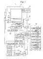
- FIG. 1is a schematic block diagram showing an embodiment of an image pickup apparatus to which the present invention is applied;
- FIGS. 2 and 3plot a relation between the quantity of light incident to the solid-state image pickup device of the illustrative embodiment shown in FIG. 1 and the quantity of digital signals when set at its lower and higher ISO sensitivity levels, respectively;
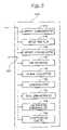
- FIG. 4is a flowchart useful for understanding the operation of the image pickup apparatus of the illustrative embodiment
- FIG. 5is a schematic block diagram showing an alternative embodiment of a signal processor
- FIG. 6is a flow chart useful for understanding the operation of the image pickup apparatus in the alternative embodiment shown in FIG. 5 .
- an illustrative embodiment 1 of an image pickup apparatus in accordance with the present inventionincludes a solid-state image pickup device 12 adapted for receiving an optical image incident thereto through an imaging lens, not shown, and a mechanical shutter 10 to perform photoelectrical conversion.
- the solid-state image pickup device 12is a camera image sensor, which is placed on the focal plane of the imaging lens and converts an optical image formed on the focal plane to electric signal charges corresponding thereto.
- the solid-state image pickup device 12 in the embodimentreads out to a vertical transfer path the signal charges generated in a bi-dimensional array of photosensitive cells 100 arranged in the horizontal and vertical scanning directions of the imaging area, and vertically transfers them in response to vertical transfer pulses V 1 -V 4 fed from a vertical driver 110 toward a horizontal transfer path 102 .
- the horizontal transfer path 102is driven by the horizontal transfer pulses H 1 and H 2 fed from a horizontal driver 112 and horizontally transfers the signal charges from the vertical transfer path toward an output amplifier 106 .
- the output amplifier 106sequentially detects the signal charges in response to the reset pulses fed from the output amplifier driver 114 and outputs pixel signals corresponding to the detected signal charges to its output 101 , which constitutes an output of the solid-state image pickup device 12 . In this way, pixel signals corresponding to an optical image captured by the solid-state image pickup device 12 are generated.
- the mechanical shutter 10 exposing the solid-state image pickup device 12 with incident lightis controlled for its releasing period of time, or exposure time, by a drive signal fed from a shutter driver 120 .
- the vertical driver 110 , horizontal transfer path 102 , output amplifier driver 114 and shutter driver 120are responsive to respective timing signals fed from a timing generator (TG) 122 to produce drive signals.
- TGtiming generator
- the output amplifier 106has its output 108 connected to an analog gain circuit 130 via a correlated double sampling (CDS) circuit not shown in the figure.
- the analog gain circuit 130is a variable-gain amplifier for variably amplifying the output of the solid-state image pickup device 12 with its gain variable, and has its input 108 also connected to receive an output of a clamp circuit 132 in a feeding back manner so that a pixel signal clamped at a predetermined level is inputted therein.
- the gain of the analog gain circuit 130is controlled with a control output of a control circuit 134 , which is implemented by a central processor unit (CPU).
- CPUcentral processor unit
- the analog gain circuit 130has its output 131 connected to an analog-to-digital converter (A/D) 136 , which converts the pixel signal to a corresponding digital signal, which will once be stored in an image memory 138 and thereafter fed to a digital signal processor (DSP) 140 . Further, the analog-to-digital converter 136 outputs a feedback signal to the clamp circuit 132 , while the clamp circuit 132 generates a feedback signal according to a value set by a setting register 142 , where a value set according to the ISO (International Organization for Standardization) sensitivity is stored, and delivers it to the input of the analog gain circuit 130 .
- A/Danalog-to-digital converter
- DSPdigital signal processor
- a value to be set by the setting register 142is, for example a value 128 in the case of the photo-sensitivity being set to ISO100-ISO800 and a value 256 in the case of the sensitivity being set to ISO1600 in the illustrative embodiment as shown in the figure.
- Gain control in the analog gain circuit 130is set according to a value stored in another setting register 144 .
- the other setting register 144 in the illustrative embodimenthas stored setting information for setting ISO100, ISO200, ISO400, ISO800 and ISO1600, as shown in the figure and set them in the analog gain circuit 130 according to instructions fed from the control circuit 134 .
- the plurality of sensitivity values setare merely illustrative, and an arrangement may be made forsetting other values of sensitivity, such as ISO64, ISO3200, etc.
- the digital signal processor (DSP) 140 connected to the image memory 138comprises a noise reducer 142 for removing noise from signals, an offset compensator 144 for compensating for an offset of signals, a white balance (WB) adjuster 146 for adjusting white balance, a gamma corrector 148 for performing gamma correction, a synchronizer 150 for performing synchronization on image signals, a contour enhancement part 152 for enhancing a contour or edge, a coloration enhancement part 154 for adjusting saturation of color, and a compressor 156 for compression-coding image data, which are interconnected via a common bus 160 to the control circuit 134 and the image memory 138 . Also, connected to the image memory 138 there is a card interface (I/F) 164 for interfacing a memory card 162 .
- I/Fcard interface
- the control circuit 134is adapted for controlling the image pickup apparatus 1 according to operational information inputted into its operational panel, not shown in the figure.
- the control circuit 134controls, for example, the start-up of the exposure value calculation and the focal adjustment control necessary for photographing, and further defines the starting of a shutter release to the constituent elements, such as the timing generator 122 , to control the period of an exposure time.
- the control circuit 134has a function to set the ISO sensitivity according to the operational information fed by the operational panel.
- FIG. 2plots a relation between the quantity of the light incident to the solid-state image pickup device 12 and the quantity of digital signals in the case of being set to a lower ISO sensitivity level.
- the horizontal axisrepresents the quantities of incident light normalized at respective ISO sensitivity levels
- the vertical axisrepresents signal levels and noise quantities ( ⁇ ) after corrected in black level and adjusted in white balance without reducing noise.
- FIG. 3plots a relation between the quantity of light incident to the solid-state image pickup device 12 and the quantity of digital signals in the case of being set to a higher ISO sensitivity level.
- a (G)is larger than a (R) and a (B).
- IRInfrared Ray
- CCD color filterCCD color filter
- photodiodes embedded in the CCDetc.
- a (G)is imparted at a ratio of 1.2* iso
- a (R)is imparted at a ratio of 1.8* iso
- a (B)at a ratio of 2.0* iso
- the above-described negative effect in the second casevaries.
- the above-described negative effect in the second casevaries in such a way that the black levels in the G and B channels rise higher than that in the R channel in the lower brightness so as to be G, B>R, resulting in change to red (R).
- the negative effect in the second case described abovemay be generalized in a way that coloration of channels having much noise occurs in the vicinity of the black level and coloration of channels having less noise occurs in the vicinity of the white level.
- FIGS. 2 and 3show examples calculated by modeling the generation of noise of random nature.
- the noise pixels lower than the mean valueare clipped to zero. Consequently, even when noise reduction, such as smoothing, takes place thereafter, it appears that a color signal having much noise stands out. More specifically, characteristic degradation occurs, in which the color turns to a color with gain increased depending upon the white balance position, while the color turns to a color opponent thereto in the case of being clipped to a higher level of brightness.
- photographingis started in response to depressing a shutter release button provided in the operational panel not shown.
- the exposure of an imaging fieldis started and the mechanical shutter, not shown, is closed after exposure for a predetermined period of time.
- the shift gate not shownis opened to read out or develop signal charges representative of captured images to the vertical transfer path. Over each of the vertical transfer paths, the signal charges for the pixels associated therewith are transferred in four phases, while two-phase transfer takes place over the horizontal transfer path (HCCD).
- HCCDhorizontal transfer path
- photographing in the illustrative embodimentincludes a case of photographing to obtain, for example, darkest image data, i.e. light-shielded data, which may preferably be processed, for example in signal processing and used in signal processing and the like.
- optical black (OB) clampingtakes place for every horizontal scanning line to bring the black level in a given value with an offset (for example, the median value “128” in the 12-bit system, or others).
- an offsetfor example, the median value “128” in the 12-bit system, or others.
- the gain in accordance with ISO sensitivity settingis adjusted to amplify a signal to then deliver it to the analog-to-digital converter, where analog-to-digital conversion is performed.
- the converted image dataare written in the image memory 138 .
- the clamp levelis increased from a value, for example, 128 to 256, depending upon the set ISO sensitivity, a higher temperature and an exposure for a longer period of time to thereby prevent ones of the noise pixels of a brightness lower than the mean value from being clipped.
- step 400 shown in FIG. 4it is determined whether or not the ISO sensitivity is higher than a predetermined value, ISO1600 with the illustrative embodiment, and if the sensitivity has been set to ISO1600 or more, then the procedure proceeds to step 402 , and otherwise to step 404 .
- step 404it is further determined whether or not the temperature is higher than a predetermined value. If the temperature is higher than the predetermined value, then the procedure proceeds to step 402 , and otherwise to step 406 .
- step 406it is determined whether or not the shutter speed, i.e. the shutter release period of time of the mechanical shutter is of a long-time exposure, for example, for 30 second or more. When it is 30 second or more, the procedure proceeds to step 402 , and otherwise it proceeds to step 408 .
- step 408a clamp level in the clamp circuit 132 is set to a value “128”.
- step 402followed by steps 400 - 406 , an estimation of the noise quantity ( ⁇ ) takes place according to the results of determining conditions in steps 400 - 406 .
- step 410it is determined whether or not a clamp quantity about three times as much as the noise quantity ( ⁇ ) estimated in step 402 is secured.
- step 412the clamp level is set to a value “256”. After that, the procedure proceeds to step 414 .
- step 414noise reduction is executed.
- noise reductionis taken place by the noise reducer 142 while the black level is maintained.
- Noise reductionremoves noise of random nature, such as of smoothened, median type and the like. In this process, pixel clipping due to inevitable random noise, such as amplifier noise, optical shot noise, etc., is prevented.
- black level or offset compensationis executed in step 416
- gamma correctionis executed in step 418
- synchronizationis executed in step 420 . After those processes, white balance adjustment takes place.
- the image data thus processedare compress-coded by the compressor 156 and recorded in, for example, the memory card 162 connected to the card interface 164 .
- the configurationin which a clamp level is controlled to be increased at the time of photographing under a predetermined exposure condition, such as a super high-sensitivity mode, a high temperature, long-time exposure, etc., then noise reduction for removing random noise takes place prior to black level adjustment and thereafter the black level is adjusted. It is therefore possible to prevent noise clipping in the analog and digital systems of the image pickup apparatus. In such a case, even when the clamp level is not increased, an advantageous effect can be obtained in respect of prevention of noise clipping in the digital system.
- the image pickup apparatus in accordance with the alternative embodimentmay be the same as the image pickup apparatus 1 shown in FIG. 1 except that the former includes a signal processor for compensating for a defect in an image prior to reducing noise in step 414 , FIG. 4 , while the remaining configuration may be the same as the image pickup apparatus 1 .
- the signal processor 500 in the alternative embodimentis shown in FIG. 5 .
- the signal processor 500may be identical with the signal processor 140 except that it includes a defect compensator 510 in addition to the configuration of the signal processor 140 in the image pickup apparatus 1 shown in FIG. 1 , while the remaining structure may be similar to that of the signal processor 140 shown in FIG. 1 , description of which will thus not be repeated.
- the defect compensator 510 in the alternative embodimentis adapted to correct image data in terms of removal of high-frequency fixed pattern noise involved in the black level such as compensation of an image defect such as a spot- or scratch-like defect, compensation of a vertical line defect and correction of an inter-field step (a horizontal line defect).
- image datain terms of removal of high-frequency fixed pattern noise involved in the black level such as compensation of an image defect such as a spot- or scratch-like defect, compensation of a vertical line defect and correction of an inter-field step (a horizontal line defect).
- an offset from the primary black levelmay preferably be corrected.
- FIG. 6there is shown an operational flow of the image pickup apparatus in the alternative embodiment. What is different from the operation described in FIG. 4 is that noise reduction takes place followed by step 412 and thereafter, black level correction takes place in the following step 414 .
- the processing operations similar to those shown in FIG. 4are denoted with the same reference numerals, description of which will thus not be repetitive.
- step 600the digital signal processor 140 first removes frequency noise accompanied with the black level, such as compensation of a defect, compensation of a vertical line defect, correction of an inter-field step (horizontal line defect), etc.
- frequency noiseaccompanied with the black level
- the black levelsuch as compensation of a defect, compensation of a vertical line defect, correction of an inter-field step (horizontal line defect), etc.
- light-shielded datawhich are obtained with light shielded, are possibly subtracted, in which case subtraction is executed only for a differential form, i.e. on a difference from the primary or basic black level, for example, with the primary black level (e.g. “128” or “256”) maintained as well.
- noise reduction intended for removal of noise of random natureis executed in a similar manner to that in the illustrative embodiment shown in FIG. 1 , and thereafter, the primary black is corrected.
- Image defectsas being generally called as “white defect”, tend to rise in gradation. Therefore, when they are smoothened rather than removed, the black falls to a further extend like in noise clipping.
- AVBautomatic white balance adjustment
- AFautomatic focusing
- the signal processors 140 and 500 in the image pickup apparatus shown in FIGS. 1 and 5are provided with a white balance adjustor 146 .
- integrationis performed with the black level maintained in a manner described in connection with the above illustrative embodiments, and then the primary black level is subtracted from the image data.
- the white balance corrector 146For example, on the consumption of 0 ⁇ i and j ⁇ 8, integration with 64-division is performed by the white balance corrector 146 . If integration data with area divided used in automatic white balancing and the like are acquired after the correction of the black level before noise reduction, an optimum white balance coefficient cannot be obtained, since this results in obtaining a white balance coefficient based on the raised black level. On the other hand, to acquire integration data, integration is performed for pixels in the same area color by color. As a result, a noise reduction effect similar to that in the averaging procedure can be obtained. Accordingly, in the instant alternative embodiment, by obtaining integration data while not correcting the black level but by thereafter correcting the black level based on the obtained integration data, it is possible to obtain an optimum white balance coefficient. Also, based on the same principle, integration data during a photometric operation can be obtained, so that a rise in black level can be prevented from occurring, and therefore, exposure control, which would otherwise decrease exposure, is not needed.
Landscapes
- Engineering & Computer Science (AREA)
- Multimedia (AREA)
- Signal Processing (AREA)
- Studio Devices (AREA)
- Color Television Image Signal Generators (AREA)
- Transforming Light Signals Into Electric Signals (AREA)
Abstract
Description
Total_Noise=SQRT(a* Sig+(a* Noise)^2), (1)
where,a represents gain, a=ISO sensitivity gain * WB gain=iso * wb, while Sig is a signal level of a digital image (after adjusted in white balance) and the Noise represents dark noise.
Total_Noise (R)=SQRT(100a(R^2+1000a(R)), (2)
Total_Noise (G)=SQRT(100a(R^2+1000a(G)), (3)
Total_Noise (B)=SQRT(100a(R^2+1000a(B)), (4)
where R, G and B represent red, green and blue, respectively.
Total_Noise (G)<Total_Noise (R), (5)
Total_Noise (G)<Total_Noise (B). (6)
Data (x, y) after defect compensation=Data (x, y)−(Dark (x, y)−128). (7)
R[i, j]=Σdata—R(x, y)−128, (8)
G[i, j]=Σdata—G(x, y)−128, (9)
B[i, j]=Σdata—B(x, y)−128, (10)
R/G[i, j]=R[i, j]/G[i, j], (11)
B/G[i, j]=B[i, j]/G[i, j]. (12)
Claims (11)
Applications Claiming Priority (2)
| Application Number | Priority Date | Filing Date | Title |
|---|---|---|---|
| JP2005299892AJP4773179B2 (en) | 2005-10-14 | 2005-10-14 | Imaging device |
| JP2005-299892 | 2005-10-14 |
Publications (2)
| Publication Number | Publication Date |
|---|---|
| US20070085917A1 US20070085917A1 (en) | 2007-04-19 |
| US7692699B2true US7692699B2 (en) | 2010-04-06 |
Family
ID=37947792
Family Applications (1)
| Application Number | Title | Priority Date | Filing Date |
|---|---|---|---|
| US11/545,538Active2028-07-12US7692699B2 (en) | 2005-10-14 | 2006-10-11 | Image pickup apparatus for preventing linearity defect |
Country Status (2)
| Country | Link |
|---|---|
| US (1) | US7692699B2 (en) |
| JP (1) | JP4773179B2 (en) |
Cited By (4)
| Publication number | Priority date | Publication date | Assignee | Title |
|---|---|---|---|---|
| US20100054587A1 (en)* | 2008-08-26 | 2010-03-04 | Canon Kabushiki Kaisha | Image processing apparatus and image processing method |
| US20100321541A1 (en)* | 2005-04-27 | 2010-12-23 | Nikon Corporation | Noise reducing device, electronic camera, and image processing program for reducing image noise by using blackout image |
| US20120105669A1 (en)* | 2010-10-27 | 2012-05-03 | Panasonic Corporation | Imaging apparatus |
| US20140085504A1 (en)* | 2011-06-30 | 2014-03-27 | Fujifilm Corporation | Imaging device, control method for imaging device, and storage medium storing a control program for imaging device |
Families Citing this family (70)
| Publication number | Priority date | Publication date | Assignee | Title |
|---|---|---|---|---|
| KR101379256B1 (en)* | 2007-07-09 | 2014-04-02 | 삼성전자주식회사 | Method and apparatus for compensating signal distortion by noise |
| US11792538B2 (en) | 2008-05-20 | 2023-10-17 | Adeia Imaging Llc | Capturing and processing of images including occlusions focused on an image sensor by a lens stack array |
| US8866920B2 (en) | 2008-05-20 | 2014-10-21 | Pelican Imaging Corporation | Capturing and processing of images using monolithic camera array with heterogeneous imagers |
| DK3876510T3 (en) | 2008-05-20 | 2024-11-11 | Adeia Imaging Llc | CAPTURE AND PROCESSING OF IMAGES USING MONOLITHIC CAMERA ARRAY WITH HETEROGENEOUS IMAGES |
| WO2010030574A1 (en)* | 2008-09-11 | 2010-03-18 | Zoran Corporation | Method and apparatus for post noise reduction black level correction |
| JP5401191B2 (en) | 2009-07-21 | 2014-01-29 | 富士フイルム株式会社 | Imaging apparatus and signal processing method |
| EP2502115A4 (en) | 2009-11-20 | 2013-11-06 | Pelican Imaging Corp | CAPTURE AND IMAGE PROCESSING USING A MONOLITHIC CAMERAS NETWORK EQUIPPED WITH HETEROGENEOUS IMAGERS |
| US8928793B2 (en) | 2010-05-12 | 2015-01-06 | Pelican Imaging Corporation | Imager array interfaces |
| JP5088408B2 (en)* | 2010-09-22 | 2012-12-05 | 株式会社ニコン | Image processing apparatus, image processing program, and electronic camera |
| JP5153846B2 (en)* | 2010-09-28 | 2013-02-27 | キヤノン株式会社 | Image processing apparatus, imaging apparatus, image processing method, and program |
| US8878950B2 (en) | 2010-12-14 | 2014-11-04 | Pelican Imaging Corporation | Systems and methods for synthesizing high resolution images using super-resolution processes |
| EP2708019B1 (en) | 2011-05-11 | 2019-10-16 | FotoNation Limited | Systems and methods for transmitting and receiving array camera image data |
| US20130265459A1 (en) | 2011-06-28 | 2013-10-10 | Pelican Imaging Corporation | Optical arrangements for use with an array camera |
| KR20140045458A (en) | 2011-06-28 | 2014-04-16 | 펠리칸 이매징 코포레이션 | Optical arrangements for use with an array camera |
| JP2013030832A (en)* | 2011-07-26 | 2013-02-07 | Toshiba Corp | Black level adjustment control device and solid-state imaging device |
| US20130070060A1 (en) | 2011-09-19 | 2013-03-21 | Pelican Imaging Corporation | Systems and methods for determining depth from multiple views of a scene that include aliasing using hypothesized fusion |
| CN104081414B (en) | 2011-09-28 | 2017-08-01 | Fotonation开曼有限公司 | Systems and methods for encoding and decoding light field image files |
| EP2817955B1 (en) | 2012-02-21 | 2018-04-11 | FotoNation Cayman Limited | Systems and methods for the manipulation of captured light field image data |
| US9210392B2 (en) | 2012-05-01 | 2015-12-08 | Pelican Imaging Coporation | Camera modules patterned with pi filter groups |
| JP2015534734A (en) | 2012-06-28 | 2015-12-03 | ペリカン イメージング コーポレイション | System and method for detecting defective camera arrays, optical arrays, and sensors |
| US20140002674A1 (en) | 2012-06-30 | 2014-01-02 | Pelican Imaging Corporation | Systems and Methods for Manufacturing Camera Modules Using Active Alignment of Lens Stack Arrays and Sensors |
| PL4296963T3 (en) | 2012-08-21 | 2025-04-28 | Adeia Imaging Llc | Method for depth detection in images captured using array cameras |
| WO2014032020A2 (en) | 2012-08-23 | 2014-02-27 | Pelican Imaging Corporation | Feature based high resolution motion estimation from low resolution images captured using an array source |
| US9214013B2 (en) | 2012-09-14 | 2015-12-15 | Pelican Imaging Corporation | Systems and methods for correcting user identified artifacts in light field images |
| EP4307659A1 (en) | 2012-09-28 | 2024-01-17 | Adeia Imaging LLC | Generating images from light fields utilizing virtual viewpoints |
| WO2014078443A1 (en)* | 2012-11-13 | 2014-05-22 | Pelican Imaging Corporation | Systems and methods for array camera focal plane control |
| US9462164B2 (en) | 2013-02-21 | 2016-10-04 | Pelican Imaging Corporation | Systems and methods for generating compressed light field representation data using captured light fields, array geometry, and parallax information |
| US9374512B2 (en) | 2013-02-24 | 2016-06-21 | Pelican Imaging Corporation | Thin form factor computational array cameras and modular array cameras |
| US9774789B2 (en) | 2013-03-08 | 2017-09-26 | Fotonation Cayman Limited | Systems and methods for high dynamic range imaging using array cameras |
| US8866912B2 (en) | 2013-03-10 | 2014-10-21 | Pelican Imaging Corporation | System and methods for calibration of an array camera using a single captured image |
| US9521416B1 (en) | 2013-03-11 | 2016-12-13 | Kip Peli P1 Lp | Systems and methods for image data compression |
| US9106784B2 (en) | 2013-03-13 | 2015-08-11 | Pelican Imaging Corporation | Systems and methods for controlling aliasing in images captured by an array camera for use in super-resolution processing |
| US9888194B2 (en) | 2013-03-13 | 2018-02-06 | Fotonation Cayman Limited | Array camera architecture implementing quantum film image sensors |
| WO2014165244A1 (en) | 2013-03-13 | 2014-10-09 | Pelican Imaging Corporation | Systems and methods for synthesizing images from image data captured by an array camera using restricted depth of field depth maps in which depth estimation precision varies |
| US9124831B2 (en) | 2013-03-13 | 2015-09-01 | Pelican Imaging Corporation | System and methods for calibration of an array camera |
| WO2014153098A1 (en) | 2013-03-14 | 2014-09-25 | Pelican Imaging Corporation | Photmetric normalization in array cameras |
| US9578259B2 (en) | 2013-03-14 | 2017-02-21 | Fotonation Cayman Limited | Systems and methods for reducing motion blur in images or video in ultra low light with array cameras |
| US9438888B2 (en) | 2013-03-15 | 2016-09-06 | Pelican Imaging Corporation | Systems and methods for stereo imaging with camera arrays |
| US9633442B2 (en) | 2013-03-15 | 2017-04-25 | Fotonation Cayman Limited | Array cameras including an array camera module augmented with a separate camera |
| US9497429B2 (en) | 2013-03-15 | 2016-11-15 | Pelican Imaging Corporation | Extended color processing on pelican array cameras |
| WO2014150856A1 (en) | 2013-03-15 | 2014-09-25 | Pelican Imaging Corporation | Array camera implementing quantum dot color filters |
| US9445003B1 (en) | 2013-03-15 | 2016-09-13 | Pelican Imaging Corporation | Systems and methods for synthesizing high resolution images using image deconvolution based on motion and depth information |
| US10122993B2 (en) | 2013-03-15 | 2018-11-06 | Fotonation Limited | Autofocus system for a conventional camera that uses depth information from an array camera |
| US9898856B2 (en) | 2013-09-27 | 2018-02-20 | Fotonation Cayman Limited | Systems and methods for depth-assisted perspective distortion correction |
| US9264592B2 (en) | 2013-11-07 | 2016-02-16 | Pelican Imaging Corporation | Array camera modules incorporating independently aligned lens stacks |
| US10119808B2 (en) | 2013-11-18 | 2018-11-06 | Fotonation Limited | Systems and methods for estimating depth from projected texture using camera arrays |
| WO2015081279A1 (en) | 2013-11-26 | 2015-06-04 | Pelican Imaging Corporation | Array camera configurations incorporating multiple constituent array cameras |
| US10089740B2 (en) | 2014-03-07 | 2018-10-02 | Fotonation Limited | System and methods for depth regularization and semiautomatic interactive matting using RGB-D images |
| US9247117B2 (en) | 2014-04-07 | 2016-01-26 | Pelican Imaging Corporation | Systems and methods for correcting for warpage of a sensor array in an array camera module by introducing warpage into a focal plane of a lens stack array |
| US9521319B2 (en) | 2014-06-18 | 2016-12-13 | Pelican Imaging Corporation | Array cameras and array camera modules including spectral filters disposed outside of a constituent image sensor |
| JP2017531976A (en) | 2014-09-29 | 2017-10-26 | フォトネイション ケイマン リミテッド | System and method for dynamically calibrating an array camera |
| US9942474B2 (en) | 2015-04-17 | 2018-04-10 | Fotonation Cayman Limited | Systems and methods for performing high speed video capture and depth estimation using array cameras |
| US10482618B2 (en) | 2017-08-21 | 2019-11-19 | Fotonation Limited | Systems and methods for hybrid depth regularization |
| JP7134786B2 (en)* | 2018-08-27 | 2022-09-12 | キヤノン株式会社 | Imaging device and control method |
| US11270110B2 (en) | 2019-09-17 | 2022-03-08 | Boston Polarimetrics, Inc. | Systems and methods for surface modeling using polarization cues |
| WO2021071992A1 (en) | 2019-10-07 | 2021-04-15 | Boston Polarimetrics, Inc. | Systems and methods for augmentation of sensor systems and imaging systems with polarization |
| DE112020005932T5 (en) | 2019-11-30 | 2023-01-05 | Boston Polarimetrics, Inc. | SYSTEMS AND METHODS FOR SEGMENTATION OF TRANSPARENT OBJECTS USING POLARIZATION CHARACTERISTICS |
| EP4081933A4 (en) | 2020-01-29 | 2024-03-20 | Intrinsic Innovation LLC | Systems and methods for characterizing object pose detection and measurement systems |
| US11797863B2 (en) | 2020-01-30 | 2023-10-24 | Intrinsic Innovation Llc | Systems and methods for synthesizing data for training statistical models on different imaging modalities including polarized images |
| US11953700B2 (en) | 2020-05-27 | 2024-04-09 | Intrinsic Innovation Llc | Multi-aperture polarization optical systems using beam splitters |
| US12020455B2 (en) | 2021-03-10 | 2024-06-25 | Intrinsic Innovation Llc | Systems and methods for high dynamic range image reconstruction |
| US12069227B2 (en) | 2021-03-10 | 2024-08-20 | Intrinsic Innovation Llc | Multi-modal and multi-spectral stereo camera arrays |
| US11954886B2 (en) | 2021-04-15 | 2024-04-09 | Intrinsic Innovation Llc | Systems and methods for six-degree of freedom pose estimation of deformable objects |
| US11290658B1 (en) | 2021-04-15 | 2022-03-29 | Boston Polarimetrics, Inc. | Systems and methods for camera exposure control |
| US12067746B2 (en) | 2021-05-07 | 2024-08-20 | Intrinsic Innovation Llc | Systems and methods for using computer vision to pick up small objects |
| US12175741B2 (en) | 2021-06-22 | 2024-12-24 | Intrinsic Innovation Llc | Systems and methods for a vision guided end effector |
| US12340538B2 (en) | 2021-06-25 | 2025-06-24 | Intrinsic Innovation Llc | Systems and methods for generating and using visual datasets for training computer vision models |
| US12172310B2 (en) | 2021-06-29 | 2024-12-24 | Intrinsic Innovation Llc | Systems and methods for picking objects using 3-D geometry and segmentation |
| US11689813B2 (en) | 2021-07-01 | 2023-06-27 | Intrinsic Innovation Llc | Systems and methods for high dynamic range imaging using crossed polarizers |
| US12293535B2 (en) | 2021-08-03 | 2025-05-06 | Intrinsic Innovation Llc | Systems and methods for training pose estimators in computer vision |
Citations (6)
| Publication number | Priority date | Publication date | Assignee | Title |
|---|---|---|---|---|
| US4412246A (en)* | 1981-07-13 | 1983-10-25 | Hamamatsu Systems, Inc. | Method of adjusting a video microscope system incorporating polarization or interference optics for optimum imaging conditions |
| US5512947A (en)* | 1993-03-31 | 1996-04-30 | Fuji Photo Film Co., Ltd. | Video camera |
| US5841488A (en)* | 1995-12-28 | 1998-11-24 | Thomson Consumer Electronics, Inc. | Multiple video input clamping arrangement |
| US6304292B1 (en)* | 1996-01-12 | 2001-10-16 | Sanyo Electric Co., Ltd. | Digital video camera with high-speed mode |
| JP2003319267A (en) | 2002-04-19 | 2003-11-07 | Nikon Corp | Digital camera |
| US20040252204A1 (en)* | 2003-01-31 | 2004-12-16 | Haruhisa Kurane | Digital clamping circuit and digital clamping method |
Family Cites Families (1)
| Publication number | Priority date | Publication date | Assignee | Title |
|---|---|---|---|---|
| JP2005101985A (en)* | 2003-09-25 | 2005-04-14 | Sony Corp | Solid-state image pickup device and image input device |
- 2005
- 2005-10-14JPJP2005299892Apatent/JP4773179B2/ennot_activeExpired - Fee Related
- 2006
- 2006-10-11USUS11/545,538patent/US7692699B2/enactiveActive
Patent Citations (6)
| Publication number | Priority date | Publication date | Assignee | Title |
|---|---|---|---|---|
| US4412246A (en)* | 1981-07-13 | 1983-10-25 | Hamamatsu Systems, Inc. | Method of adjusting a video microscope system incorporating polarization or interference optics for optimum imaging conditions |
| US5512947A (en)* | 1993-03-31 | 1996-04-30 | Fuji Photo Film Co., Ltd. | Video camera |
| US5841488A (en)* | 1995-12-28 | 1998-11-24 | Thomson Consumer Electronics, Inc. | Multiple video input clamping arrangement |
| US6304292B1 (en)* | 1996-01-12 | 2001-10-16 | Sanyo Electric Co., Ltd. | Digital video camera with high-speed mode |
| JP2003319267A (en) | 2002-04-19 | 2003-11-07 | Nikon Corp | Digital camera |
| US20040252204A1 (en)* | 2003-01-31 | 2004-12-16 | Haruhisa Kurane | Digital clamping circuit and digital clamping method |
Cited By (8)
| Publication number | Priority date | Publication date | Assignee | Title |
|---|---|---|---|---|
| US20100321541A1 (en)* | 2005-04-27 | 2010-12-23 | Nikon Corporation | Noise reducing device, electronic camera, and image processing program for reducing image noise by using blackout image |
| US7956909B2 (en)* | 2005-04-27 | 2011-06-07 | Nikon Corporation | Noise reducing device, electronic camera, and image processing program for reducing image noise by using blackout image |
| US20100054587A1 (en)* | 2008-08-26 | 2010-03-04 | Canon Kabushiki Kaisha | Image processing apparatus and image processing method |
| US8229214B2 (en)* | 2008-08-26 | 2012-07-24 | Canon Kabushiki Kaisha | Image processing apparatus and image processing method |
| US20120105669A1 (en)* | 2010-10-27 | 2012-05-03 | Panasonic Corporation | Imaging apparatus |
| US9030574B2 (en)* | 2010-10-27 | 2015-05-12 | Panasonic Intellectual Property Management Co., Ltd. | Imaging apparatus capable of correcting white balance based on an output signal amplification gain and white balance gain |
| US20140085504A1 (en)* | 2011-06-30 | 2014-03-27 | Fujifilm Corporation | Imaging device, control method for imaging device, and storage medium storing a control program for imaging device |
| US8922684B2 (en)* | 2011-06-30 | 2014-12-30 | Fujifilm Corporation | Imaging device, control method for imaging device, and storage medium storing a control program for imaging device |
Also Published As
| Publication number | Publication date |
|---|---|
| US20070085917A1 (en) | 2007-04-19 |
| JP2007110486A (en) | 2007-04-26 |
| JP4773179B2 (en) | 2011-09-14 |
Similar Documents
| Publication | Publication Date | Title |
|---|---|---|
| US7692699B2 (en) | Image pickup apparatus for preventing linearity defect | |
| US7508975B2 (en) | Image sensor | |
| KR100617781B1 (en) | Device and method for improving image quality of image sensor | |
| US7545420B2 (en) | Image sensing apparatus, image sensing method, and program | |
| KR100880085B1 (en) | Imager and noise reduction method | |
| CN102572273B (en) | Camera head | |
| CN102883108B (en) | Picture pick-up device and control method, image processing equipment and method | |
| US20040262492A1 (en) | Solid-state image sensing apparatus | |
| WO2011025526A1 (en) | Image capture device | |
| US20040239790A1 (en) | Image capturing apparatus | |
| US8379116B2 (en) | Image pick-up apparatus and image processing method | |
| JP4719442B2 (en) | Image signal processing circuit, camera, and image signal processing method | |
| US8144210B2 (en) | White balance adjustment device and white balance adjustment method | |
| JP2010200109A (en) | Imaging device, control method, and program | |
| US8564694B2 (en) | Image pickup device and noise reduction method thereof | |
| JP4872502B2 (en) | Imaging apparatus and clamping method thereof | |
| JP2011009834A (en) | Imager and imaging method | |
| JP4732795B2 (en) | Solid-state imaging device and image correction method | |
| JPH11215431A (en) | Television camera | |
| JP2010178384A (en) | Image signal processing circuit, camera and image signal processing method | |
| JP2011049737A (en) | Imaging apparatus and exposure control method thereof | |
| JP2006157341A (en) | Smear correcting method and signal processor for solid-state imaging device, and imaging apparatus | |
| JP4415753B2 (en) | Imaging apparatus and imaging method | |
| JP2011055336A (en) | Imaging apparatus and signal processing method | |
| JP2005033687A (en) | Defect detecting apparatus and method therefor, recording medium, as well as program |
Legal Events
| Date | Code | Title | Description |
|---|---|---|---|
| AS | Assignment | Owner name:FUJIFILM CORPORATION,JAPAN Free format text:ASSIGNMENT OF ASSIGNORS INTEREST;ASSIGNOR:KOBAYASHI, HIROKAZU;REEL/FRAME:018401/0576 Effective date:20061002 Owner name:FUJIFILM CORPORATION, JAPAN Free format text:ASSIGNMENT OF ASSIGNORS INTEREST;ASSIGNOR:KOBAYASHI, HIROKAZU;REEL/FRAME:018401/0576 Effective date:20061002 | |
| FEPP | Fee payment procedure | Free format text:PAYOR NUMBER ASSIGNED (ORIGINAL EVENT CODE: ASPN); ENTITY STATUS OF PATENT OWNER: LARGE ENTITY | |
| STCF | Information on status: patent grant | Free format text:PATENTED CASE | |
| FPAY | Fee payment | Year of fee payment:4 | |
| MAFP | Maintenance fee payment | Free format text:PAYMENT OF MAINTENANCE FEE, 8TH YEAR, LARGE ENTITY (ORIGINAL EVENT CODE: M1552) Year of fee payment:8 | |
| MAFP | Maintenance fee payment | Free format text:PAYMENT OF MAINTENANCE FEE, 12TH YEAR, LARGE ENTITY (ORIGINAL EVENT CODE: M1553); ENTITY STATUS OF PATENT OWNER: LARGE ENTITY Year of fee payment:12 |