US7692514B2 - Linear antenna switch arm - Google Patents
Linear antenna switch armDownload PDFInfo
- Publication number
- US7692514B2 US7692514B2US11/769,938US76993807AUS7692514B2US 7692514 B2US7692514 B2US 7692514B2US 76993807 AUS76993807 AUS 76993807AUS 7692514 B2US7692514 B2US 7692514B2
- Authority
- US
- United States
- Prior art keywords
- signal line
- antenna switch
- switch arm
- linear antenna
- signal
- Prior art date
- Legal status (The legal status is an assumption and is not a legal conclusion. Google has not performed a legal analysis and makes no representation as to the accuracy of the status listed.)
- Active, expires
Links
- 230000005669field effectEffects0.000claimsabstractdescription7
- 230000000295complement effectEffects0.000claimsabstractdescription3
- 239000008186active pharmaceutical agentSubstances0.000description2
- 230000001413cellular effectEffects0.000description1
- 238000000034methodMethods0.000description1
Images


Classifications
- H—ELECTRICITY
- H03—ELECTRONIC CIRCUITRY
- H03K—PULSE TECHNIQUE
- H03K17/00—Electronic switching or gating, i.e. not by contact-making and –breaking
- H03K17/10—Modifications for increasing the maximum permissible switched voltage
- H03K17/102—Modifications for increasing the maximum permissible switched voltage in field-effect transistor switches
- H—ELECTRICITY
- H03—ELECTRONIC CIRCUITRY
- H03K—PULSE TECHNIQUE
- H03K17/00—Electronic switching or gating, i.e. not by contact-making and –breaking
- H03K17/51—Electronic switching or gating, i.e. not by contact-making and –breaking characterised by the components used
- H03K17/56—Electronic switching or gating, i.e. not by contact-making and –breaking characterised by the components used by the use, as active elements, of semiconductor devices
- H03K17/687—Electronic switching or gating, i.e. not by contact-making and –breaking characterised by the components used by the use, as active elements, of semiconductor devices the devices being field-effect transistors
- H03K17/6871—Electronic switching or gating, i.e. not by contact-making and –breaking characterised by the components used by the use, as active elements, of semiconductor devices the devices being field-effect transistors the output circuit comprising more than one controlled field-effect transistor
- H—ELECTRICITY
- H03—ELECTRONIC CIRCUITRY
- H03K—PULSE TECHNIQUE
- H03K17/00—Electronic switching or gating, i.e. not by contact-making and –breaking
- H03K17/51—Electronic switching or gating, i.e. not by contact-making and –breaking characterised by the components used
- H03K17/56—Electronic switching or gating, i.e. not by contact-making and –breaking characterised by the components used by the use, as active elements, of semiconductor devices
- H03K17/687—Electronic switching or gating, i.e. not by contact-making and –breaking characterised by the components used by the use, as active elements, of semiconductor devices the devices being field-effect transistors
- H03K17/693—Switching arrangements with several input- or output-terminals, e.g. multiplexers, distributors
- H—ELECTRICITY
- H04—ELECTRIC COMMUNICATION TECHNIQUE
- H04B—TRANSMISSION
- H04B1/00—Details of transmission systems, not covered by a single one of groups H04B3/00 - H04B13/00; Details of transmission systems not characterised by the medium used for transmission
- H04B1/38—Transceivers, i.e. devices in which transmitter and receiver form a structural unit and in which at least one part is used for functions of transmitting and receiving
- H04B1/40—Circuits
- H04B1/44—Transmit/receive switching
- H04B1/48—Transmit/receive switching in circuits for connecting transmitter and receiver to a common transmission path, e.g. by energy of transmitter
Definitions
- the present inventionrelates to a linear antenna switch arm. More particularly, but not exclusively, the present invention relates to a linear antenna switch arm comprising a plurality of FETs connected in series and having a resistor between input and output and at least one join node path having at least one resistor.
- Antenna switchesare used in applications requiring a time division multiple access method, for example GSM and UMTS cellular phones.
- Series shunt configurationsare often used, with a single pole and several throws, the series devices connecting alternatively either of a receive or transmit port to the single pole, and the shunt devices isolating the non-used ports.
- Field effect transistorsare used to realise the series or shunt devices, the input being the drain and the output the source, or vice-versa. The signal passes through the conductive channel.
- the signalWhen reaching the single pole, the signal “sees” one or several OFF arms in parallel.
- the voltage swing present at the polemust not turn on the FET present in the OFF arm.
- FETsare therefore used in series in order to spread the high voltage across a high number of junctions and the junctions are kept at a floating bias.
- each of the FETs constituting the OFF armcan be modelled by a highly non linear shunt capacitance, thus introducing non linearities in the switched signal.
- the present inventionseeks to overcome this problem.
- the present inventionprovides a linear antenna switch arm comprising
- the linear antenna switch armis significantly more linear than known antenna switch arms.
- connection lineseach connection line including a resistor.
- Adjacent nodescan be electrically shorted together by the signal line.
- the signal linecan comprise a resistor between signal input port and the first node in the signal line.
- the signal linecan comprise a resistor between signal output port and last node in the signal line.
- connection linescan comprise a diode.
- the signal linecan further comprise at least one diode.
- the gates of the field effect transistorsare connected to a control line by resistors.
- FIG. 1shows a known antenna switch arm
- FIG. 2shows a first embodiment of a linear antenna switch arm according to the invention
- FIG. 3shows a second embodiment of a linear antenna switch arm according to the invention
- FIG. 4shows a third embodiment of a linear antenna switch arm according to the invention.
- FIG. 5shows a fourth embodiment of a linear antenna switch arm according to the invention.
- FIG. 6shows a fifth embodiment of a linear antenna switch arm according to the invention.
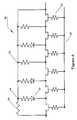
- FIG. 7shows a sixth embodiment of a linear antenna switch arm according to the invention.
- FIG. 1shows, in schematic form, a known antenna switch arm 1 .
- the antenna switch arm 1comprises first and second field effect transistors 2 , 3 connected in series with the drain 4 of one transistor 2 connected to the source 5 of the next.
- the source 6 of one transistor 2is connected to a signal input port 3 .
- the drain 8 of the otheris connected to a signal output port 9 .
- a shunt resistor 10extends between the input and output ports 7 , 9 .
- the impedance between the ports 7 , 9is R DS in parallel with C FET (the off capacitance of the FETs) which is highly non linear.
- C FETthe off capacitance of the FETs
- FIG. 2Shown in FIG. 2 is a linear antenna switch arm 10 according to the invention.
- the arm 10comprises a plurality of FETs 11 connected in series with the drain of one FET 11 being connected to the source of the next, the connections between the FETs being joins 12 .
- the source of one end transistor 11is connected to a signal input port 13 .
- the drain of the other end transistor 11is connected to a signal output port 14 .
- a signal line 15extends between the input and output ports 13 , 14 .
- One of the joins 17is connected to the signal line 15 at a node 16 by a connection line 17 .
- the connection line 17includes a resistor 18 .
- the signal line 15includes a resistor 19 between the node 16 and the output port 14 .
- connection line 17fixes the voltage at the join 12 with a high value resistor 18 . This significantly improves the linearity of the linear antenna switch arm 10 .
- FIG. 3Shown in FIG. 3 is a further embodiment of a linear antenna switch arm 10 according to the invention. This embodiment is similar to that of FIG. 2 except the resistor 19 in the signal line 15 is between the input port 13 and the node 16 .
- FIG. 4Shown in FIG. 4 is a further embodiment of a linear antenna switch arm 10 according to the invention.
- a plurality of joins 12are connected to the signal line 15 at nodes 16 by connection lines 17 .
- Each connection line 17includes a resistor 18 . Resistors are not included in the signal line 15 between the nodes 16 .
- the nodes 16are essentially short circuited together by the signal line 15 .
- the connection lines 17pin the voltages at the joins 12 so improving the linearity of the linear antenna switch arm 10 .
- FIG. 5Shown in FIG. 5 is a further embodiment of a linear antenna switch arm 10 according to the invention. This embodiment is similar to that of FIG. 4 except each of the connection lines 17 includes a diode 20 in addition to a resistor 18 .
- FIG. 6Shown in FIG. 6 is a further embodiment of a linear antenna switch arm 10 according to the invention. This embodiment is similar to the embodiment of FIG. 5 except not all of the connection line 17 include a diode 20 .
- FIG. 7Shown in FIG. 7 is a further embodiment of a linear antenna switch arm 10 according to the invention. This embodiment includes a diode 21 in the signal line.
- the gates of the FETs 11are connected to a control line 22 by resistors 23 for turning the FETs on and off.
Landscapes
- Engineering & Computer Science (AREA)
- Computer Networks & Wireless Communication (AREA)
- Signal Processing (AREA)
- Electronic Switches (AREA)
Abstract
Description
- a plurality of field effect transistors connected in series, the drain of each transistor being connected to the source of the next transistor at a join, the end source comprising one of a signal input or output port and the end drain comprising the complementary signal output port or input port;
- a signal line extending between the input and output ports;
- at least one of the joins being connected to the signal line at a node by a connection line;
- the signal line comprising at least one resistor between signal input and output ports; and
- the connection line comprising at least one resistor.
Claims (11)
Applications Claiming Priority (2)
| Application Number | Priority Date | Filing Date | Title |
|---|---|---|---|
| GB0612755.9 | 2006-06-28 | ||
| GB0612755AGB2439622B (en) | 2006-06-28 | 2006-06-28 | A linear antenna switch arm |
Publications (2)
| Publication Number | Publication Date |
|---|---|
| US20080042913A1 US20080042913A1 (en) | 2008-02-21 |
| US7692514B2true US7692514B2 (en) | 2010-04-06 |
Family
ID=36888172
Family Applications (1)
| Application Number | Title | Priority Date | Filing Date |
|---|---|---|---|
| US11/769,938Active2028-03-15US7692514B2 (en) | 2006-06-28 | 2007-06-28 | Linear antenna switch arm |
Country Status (2)
| Country | Link |
|---|---|
| US (1) | US7692514B2 (en) |
| GB (1) | GB2439622B (en) |
Cited By (3)
| Publication number | Priority date | Publication date | Assignee | Title |
|---|---|---|---|---|
| US20120157011A1 (en)* | 2010-12-21 | 2012-06-21 | Stmicroelectronics S.A. | Electronic switch and communication device including such a switch |
| US20130015717A1 (en)* | 2011-07-13 | 2013-01-17 | Dykstra Jeffrey A | Method and Apparatus for Transistor Switch Isolation |
| US20220173731A1 (en)* | 2005-07-11 | 2022-06-02 | Psemi Corporation | Circuit and method for controlling charge injection in radio frequency switches |
Citations (9)
| Publication number | Priority date | Publication date | Assignee | Title |
|---|---|---|---|---|
| US6218890B1 (en) | 1998-07-14 | 2001-04-17 | Sanyo Electric Co., Ltd. | Switching circuit device and semiconductor device |
| EP1487103A2 (en) | 2003-06-12 | 2004-12-15 | Matsushita Electric Industrial Co., Ltd. | High-frequency switching device and semiconductor device |
| US20050079829A1 (en) | 2003-10-08 | 2005-04-14 | Takashi Ogawa | Antenna switch |
| US20050263799A1 (en) | 2004-05-31 | 2005-12-01 | Matsushita Electric Industrial Co., Ltd. | Switching circuit and semiconductor device |
| US20060118951A1 (en) | 2004-12-07 | 2006-06-08 | Takashi Ogawa | Switching element, antenna switch circuit and radio frequency module using the same |
| US20060252394A1 (en) | 2005-04-21 | 2006-11-09 | Atsushi Suwa | Switching circuit |
| US20060261912A1 (en) | 2005-05-23 | 2006-11-23 | Matsushita Electric Industrial Co., Ltd. | Radio frequency switching circuit and semiconductor device including the same |
| US20070049237A1 (en) | 2005-08-30 | 2007-03-01 | Toshihiro Miura | Semiconductor integrated circuit device and high frequency power amplifier module |
| US7459988B1 (en)* | 2006-09-18 | 2008-12-02 | Rf Micro Devices, Inc. | High linearity wide dynamic range radio frequency antenna switch |
- 2006
- 2006-06-28GBGB0612755Apatent/GB2439622B/ennot_activeExpired - Fee Related
- 2007
- 2007-06-28USUS11/769,938patent/US7692514B2/enactiveActive
Patent Citations (9)
| Publication number | Priority date | Publication date | Assignee | Title |
|---|---|---|---|---|
| US6218890B1 (en) | 1998-07-14 | 2001-04-17 | Sanyo Electric Co., Ltd. | Switching circuit device and semiconductor device |
| EP1487103A2 (en) | 2003-06-12 | 2004-12-15 | Matsushita Electric Industrial Co., Ltd. | High-frequency switching device and semiconductor device |
| US20050079829A1 (en) | 2003-10-08 | 2005-04-14 | Takashi Ogawa | Antenna switch |
| US20050263799A1 (en) | 2004-05-31 | 2005-12-01 | Matsushita Electric Industrial Co., Ltd. | Switching circuit and semiconductor device |
| US20060118951A1 (en) | 2004-12-07 | 2006-06-08 | Takashi Ogawa | Switching element, antenna switch circuit and radio frequency module using the same |
| US20060252394A1 (en) | 2005-04-21 | 2006-11-09 | Atsushi Suwa | Switching circuit |
| US20060261912A1 (en) | 2005-05-23 | 2006-11-23 | Matsushita Electric Industrial Co., Ltd. | Radio frequency switching circuit and semiconductor device including the same |
| US20070049237A1 (en) | 2005-08-30 | 2007-03-01 | Toshihiro Miura | Semiconductor integrated circuit device and high frequency power amplifier module |
| US7459988B1 (en)* | 2006-09-18 | 2008-12-02 | Rf Micro Devices, Inc. | High linearity wide dynamic range radio frequency antenna switch |
Non-Patent Citations (1)
| Title |
|---|
| Search Report for Application No. GB0612755.9, date of search Oct. 4, 2007. |
Cited By (8)
| Publication number | Priority date | Publication date | Assignee | Title |
|---|---|---|---|---|
| US20220173731A1 (en)* | 2005-07-11 | 2022-06-02 | Psemi Corporation | Circuit and method for controlling charge injection in radio frequency switches |
| US11695407B2 (en)* | 2005-07-11 | 2023-07-04 | Psemi Corporation | Circuit and method for controlling charge injection in radio frequency switches |
| US20240007098A1 (en)* | 2005-07-11 | 2024-01-04 | Psemi Corporation | Circuit and Method for Controlling Charge Injection in Radio Frequency Switches |
| US12348221B2 (en)* | 2005-07-11 | 2025-07-01 | Psemi Corporation | Circuit and method for controlling charge injection in radio frequency switches |
| US20120157011A1 (en)* | 2010-12-21 | 2012-06-21 | Stmicroelectronics S.A. | Electronic switch and communication device including such a switch |
| US8981882B2 (en)* | 2010-12-21 | 2015-03-17 | Stmicroelectronics Sa | Electronic switch and communication device including such a switch |
| US20130015717A1 (en)* | 2011-07-13 | 2013-01-17 | Dykstra Jeffrey A | Method and Apparatus for Transistor Switch Isolation |
| US9124265B2 (en)* | 2011-07-13 | 2015-09-01 | Peregrine Semiconductor Corporation | Method and apparatus for transistor switch isolation |
Also Published As
| Publication number | Publication date |
|---|---|
| GB2439622B (en) | 2011-03-30 |
| US20080042913A1 (en) | 2008-02-21 |
| GB2439622A (en) | 2008-01-02 |
| GB0612755D0 (en) | 2006-08-09 |
Similar Documents
| Publication | Publication Date | Title |
|---|---|---|
| US8212604B2 (en) | T switch with high off state isolation | |
| US7532094B2 (en) | Linear antenna switch arm and a field effect transistor | |
| US8975948B2 (en) | Wide common mode range transmission gate | |
| US6987414B2 (en) | High frequency switch circuit | |
| US6094088A (en) | Radio frequency switch circuit having resistors connected to back gates of transistors | |
| US7893749B2 (en) | High frequency switch circuit having reduced input power distortion | |
| US20060261912A1 (en) | Radio frequency switching circuit and semiconductor device including the same | |
| US20090108911A1 (en) | Analog switch | |
| US7664012B2 (en) | Solid-state ethernet by-pass switch circuitry | |
| US20060252394A1 (en) | Switching circuit | |
| US20100225378A1 (en) | Radio frequency switching circuit and semiconductor device | |
| JP2008017416A (en) | High frequency switch device | |
| US8907745B2 (en) | Transistor switches with single-polarity control voltage | |
| US20140220909A1 (en) | High freuency semiconductor switch and wireless device | |
| US7692514B2 (en) | Linear antenna switch arm | |
| US20040235549A1 (en) | Individually biased transistor high frequency switch | |
| US7868694B2 (en) | Variable resistor array and amplifier circuit | |
| JP2007096609A (en) | Semiconductor switch circuit device | |
| JP2012186702A (en) | Semiconductor switch circuit | |
| KR101616597B1 (en) | High frequency switch | |
| US11677392B2 (en) | Bias networks for DC or extended low frequency capable fast stacked switches | |
| JP4842150B2 (en) | Switch device | |
| GB2475645A (en) | Field effect transistor | |
| JP4868275B2 (en) | High frequency switch circuit | |
| CN109428574B (en) | Switch circuit capable of reducing magnitude change degree of parasitic capacitance |
Legal Events
| Date | Code | Title | Description |
|---|---|---|---|
| AS | Assignment | Owner name:FILTRONIC COMPOUND SEMICONDUCTORS LIMITED, UNITED Free format text:ASSIGNMENT OF ASSIGNORS INTEREST;ASSIGNOR:LETOUX, THOMAS;REEL/FRAME:019742/0521 Effective date:20070725 Owner name:FILTRONIC COMPOUND SEMICONDUCTORS LIMITED,UNITED K Free format text:ASSIGNMENT OF ASSIGNORS INTEREST;ASSIGNOR:LETOUX, THOMAS;REEL/FRAME:019742/0521 Effective date:20070725 | |
| AS | Assignment | Owner name:RFMD (UK) LIMITED, UNITED KINGDOM Free format text:CHANGE OF NAME;ASSIGNOR:FILTRONIC COMPOUND SEMICONDUCTORS LIMITED;REEL/FRAME:022552/0462 Effective date:20080306 Owner name:RFMD (UK) LIMITED,UNITED KINGDOM Free format text:CHANGE OF NAME;ASSIGNOR:FILTRONIC COMPOUND SEMICONDUCTORS LIMITED;REEL/FRAME:022552/0462 Effective date:20080306 | |
| STCF | Information on status: patent grant | Free format text:PATENTED CASE | |
| FPAY | Fee payment | Year of fee payment:4 | |
| FEPP | Fee payment procedure | Free format text:MAINTENANCE FEE REMINDER MAILED (ORIGINAL EVENT CODE: REM.) | |
| FEPP | Fee payment procedure | Free format text:7.5 YR SURCHARGE - LATE PMT W/IN 6 MO, LARGE ENTITY (ORIGINAL EVENT CODE: M1555) | |
| MAFP | Maintenance fee payment | Free format text:PAYMENT OF MAINTENANCE FEE, 8TH YEAR, LARGE ENTITY (ORIGINAL EVENT CODE: M1552) Year of fee payment:8 | |
| AS | Assignment | Owner name:QORVO US, INC., NORTH CAROLINA Free format text:ASSIGNMENT OF ASSIGNORS INTEREST;ASSIGNOR:RFMD (UK) LIMITED;REEL/FRAME:051330/0388 Effective date:20191218 | |
| MAFP | Maintenance fee payment | Free format text:PAYMENT OF MAINTENANCE FEE, 12TH YEAR, LARGE ENTITY (ORIGINAL EVENT CODE: M1553); ENTITY STATUS OF PATENT OWNER: LARGE ENTITY Year of fee payment:12 |