US7692207B2 - Packaging designs for LEDs - Google Patents
Packaging designs for LEDsDownload PDFInfo
- Publication number
- US7692207B2 US7692207B2US11/210,013US21001305AUS7692207B2US 7692207 B2US7692207 B2US 7692207B2US 21001305 AUS21001305 AUS 21001305AUS 7692207 B2US7692207 B2US 7692207B2
- Authority
- US
- United States
- Prior art keywords
- led
- light emitting
- layer
- emitting device
- light
- Prior art date
- Legal status (The legal status is an assumption and is not a legal conclusion. Google has not performed a legal analysis and makes no representation as to the accuracy of the status listed.)
- Active, expires
Links
Images


Classifications
- H—ELECTRICITY
- H01—ELECTRIC ELEMENTS
- H01L—SEMICONDUCTOR DEVICES NOT COVERED BY CLASS H10
- H01L24/00—Arrangements for connecting or disconnecting semiconductor or solid-state bodies; Methods or apparatus related thereto
- H01L24/01—Means for bonding being attached to, or being formed on, the surface to be connected, e.g. chip-to-package, die-attach, "first-level" interconnects; Manufacturing methods related thereto
- H01L24/18—High density interconnect [HDI] connectors; Manufacturing methods related thereto
- H01L24/23—Structure, shape, material or disposition of the high density interconnect connectors after the connecting process
- H01L24/24—Structure, shape, material or disposition of the high density interconnect connectors after the connecting process of an individual high density interconnect connector
- F—MECHANICAL ENGINEERING; LIGHTING; HEATING; WEAPONS; BLASTING
- F21—LIGHTING
- F21K—NON-ELECTRIC LIGHT SOURCES USING LUMINESCENCE; LIGHT SOURCES USING ELECTROCHEMILUMINESCENCE; LIGHT SOURCES USING CHARGES OF COMBUSTIBLE MATERIAL; LIGHT SOURCES USING SEMICONDUCTOR DEVICES AS LIGHT-GENERATING ELEMENTS; LIGHT SOURCES NOT OTHERWISE PROVIDED FOR
- F21K9/00—Light sources using semiconductor devices as light-generating elements, e.g. using light-emitting diodes [LED] or lasers
- H—ELECTRICITY
- H01—ELECTRIC ELEMENTS
- H01L—SEMICONDUCTOR DEVICES NOT COVERED BY CLASS H10
- H01L2224/00—Indexing scheme for arrangements for connecting or disconnecting semiconductor or solid-state bodies and methods related thereto as covered by H01L24/00
- H01L2224/01—Means for bonding being attached to, or being formed on, the surface to be connected, e.g. chip-to-package, die-attach, "first-level" interconnects; Manufacturing methods related thereto
- H01L2224/42—Wire connectors; Manufacturing methods related thereto
- H01L2224/47—Structure, shape, material or disposition of the wire connectors after the connecting process
- H01L2224/48—Structure, shape, material or disposition of the wire connectors after the connecting process of an individual wire connector
- H01L2224/4805—Shape
- H01L2224/4809—Loop shape
- H01L2224/48091—Arched
- H—ELECTRICITY
- H01—ELECTRIC ELEMENTS
- H01L—SEMICONDUCTOR DEVICES NOT COVERED BY CLASS H10
- H01L2924/00—Indexing scheme for arrangements or methods for connecting or disconnecting semiconductor or solid-state bodies as covered by H01L24/00
- H01L2924/01—Chemical elements
- H01L2924/01006—Carbon [C]
- H—ELECTRICITY
- H01—ELECTRIC ELEMENTS
- H01L—SEMICONDUCTOR DEVICES NOT COVERED BY CLASS H10
- H01L2924/00—Indexing scheme for arrangements or methods for connecting or disconnecting semiconductor or solid-state bodies as covered by H01L24/00
- H01L2924/01—Chemical elements
- H01L2924/01012—Magnesium [Mg]
- H—ELECTRICITY
- H01—ELECTRIC ELEMENTS
- H01L—SEMICONDUCTOR DEVICES NOT COVERED BY CLASS H10
- H01L2924/00—Indexing scheme for arrangements or methods for connecting or disconnecting semiconductor or solid-state bodies as covered by H01L24/00
- H01L2924/01—Chemical elements
- H01L2924/01013—Aluminum [Al]
- H—ELECTRICITY
- H01—ELECTRIC ELEMENTS
- H01L—SEMICONDUCTOR DEVICES NOT COVERED BY CLASS H10
- H01L2924/00—Indexing scheme for arrangements or methods for connecting or disconnecting semiconductor or solid-state bodies as covered by H01L24/00
- H01L2924/01—Chemical elements
- H01L2924/01029—Copper [Cu]
- H—ELECTRICITY
- H01—ELECTRIC ELEMENTS
- H01L—SEMICONDUCTOR DEVICES NOT COVERED BY CLASS H10
- H01L2924/00—Indexing scheme for arrangements or methods for connecting or disconnecting semiconductor or solid-state bodies as covered by H01L24/00
- H01L2924/01—Chemical elements
- H01L2924/01032—Germanium [Ge]
- H—ELECTRICITY
- H01—ELECTRIC ELEMENTS
- H01L—SEMICONDUCTOR DEVICES NOT COVERED BY CLASS H10
- H01L2924/00—Indexing scheme for arrangements or methods for connecting or disconnecting semiconductor or solid-state bodies as covered by H01L24/00
- H01L2924/01—Chemical elements
- H01L2924/01033—Arsenic [As]
- H—ELECTRICITY
- H01—ELECTRIC ELEMENTS
- H01L—SEMICONDUCTOR DEVICES NOT COVERED BY CLASS H10
- H01L2924/00—Indexing scheme for arrangements or methods for connecting or disconnecting semiconductor or solid-state bodies as covered by H01L24/00
- H01L2924/01—Chemical elements
- H01L2924/01046—Palladium [Pd]
- H—ELECTRICITY
- H01—ELECTRIC ELEMENTS
- H01L—SEMICONDUCTOR DEVICES NOT COVERED BY CLASS H10
- H01L2924/00—Indexing scheme for arrangements or methods for connecting or disconnecting semiconductor or solid-state bodies as covered by H01L24/00
- H01L2924/01—Chemical elements
- H01L2924/01047—Silver [Ag]
- H—ELECTRICITY
- H01—ELECTRIC ELEMENTS
- H01L—SEMICONDUCTOR DEVICES NOT COVERED BY CLASS H10
- H01L2924/00—Indexing scheme for arrangements or methods for connecting or disconnecting semiconductor or solid-state bodies as covered by H01L24/00
- H01L2924/01—Chemical elements
- H01L2924/01051—Antimony [Sb]
- H—ELECTRICITY
- H01—ELECTRIC ELEMENTS
- H01L—SEMICONDUCTOR DEVICES NOT COVERED BY CLASS H10
- H01L2924/00—Indexing scheme for arrangements or methods for connecting or disconnecting semiconductor or solid-state bodies as covered by H01L24/00
- H01L2924/01—Chemical elements
- H01L2924/01078—Platinum [Pt]
- H—ELECTRICITY
- H01—ELECTRIC ELEMENTS
- H01L—SEMICONDUCTOR DEVICES NOT COVERED BY CLASS H10
- H01L2924/00—Indexing scheme for arrangements or methods for connecting or disconnecting semiconductor or solid-state bodies as covered by H01L24/00
- H01L2924/01—Chemical elements
- H01L2924/01079—Gold [Au]
- H—ELECTRICITY
- H01—ELECTRIC ELEMENTS
- H01L—SEMICONDUCTOR DEVICES NOT COVERED BY CLASS H10
- H01L2924/00—Indexing scheme for arrangements or methods for connecting or disconnecting semiconductor or solid-state bodies as covered by H01L24/00
- H01L2924/01—Chemical elements
- H01L2924/01082—Lead [Pb]
- H—ELECTRICITY
- H01—ELECTRIC ELEMENTS
- H01L—SEMICONDUCTOR DEVICES NOT COVERED BY CLASS H10
- H01L2924/00—Indexing scheme for arrangements or methods for connecting or disconnecting semiconductor or solid-state bodies as covered by H01L24/00
- H01L2924/10—Details of semiconductor or other solid state devices to be connected
- H01L2924/11—Device type
- H01L2924/12—Passive devices, e.g. 2 terminal devices
- H01L2924/1204—Optical Diode
- H01L2924/12041—LED
- H—ELECTRICITY
- H01—ELECTRIC ELEMENTS
- H01L—SEMICONDUCTOR DEVICES NOT COVERED BY CLASS H10
- H01L2924/00—Indexing scheme for arrangements or methods for connecting or disconnecting semiconductor or solid-state bodies as covered by H01L24/00
- H01L2924/10—Details of semiconductor or other solid state devices to be connected
- H01L2924/11—Device type
- H01L2924/12—Passive devices, e.g. 2 terminal devices
- H01L2924/1204—Optical Diode
- H01L2924/12044—OLED
- H—ELECTRICITY
- H10—SEMICONDUCTOR DEVICES; ELECTRIC SOLID-STATE DEVICES NOT OTHERWISE PROVIDED FOR
- H10H—INORGANIC LIGHT-EMITTING SEMICONDUCTOR DEVICES HAVING POTENTIAL BARRIERS
- H10H20/00—Individual inorganic light-emitting semiconductor devices having potential barriers, e.g. light-emitting diodes [LED]
- H10H20/80—Constructional details
- H10H20/83—Electrodes
- H10H20/831—Electrodes characterised by their shape
- H10H20/8314—Electrodes characterised by their shape extending at least partially onto an outer side surface of the bodies
- H—ELECTRICITY
- H10—SEMICONDUCTOR DEVICES; ELECTRIC SOLID-STATE DEVICES NOT OTHERWISE PROVIDED FOR
- H10H—INORGANIC LIGHT-EMITTING SEMICONDUCTOR DEVICES HAVING POTENTIAL BARRIERS
- H10H20/00—Individual inorganic light-emitting semiconductor devices having potential barriers, e.g. light-emitting diodes [LED]
- H10H20/80—Constructional details
- H10H20/85—Packages
- H10H20/852—Encapsulations
- H10H20/854—Encapsulations characterised by their material, e.g. epoxy or silicone resins
- H—ELECTRICITY
- H10—SEMICONDUCTOR DEVICES; ELECTRIC SOLID-STATE DEVICES NOT OTHERWISE PROVIDED FOR
- H10H—INORGANIC LIGHT-EMITTING SEMICONDUCTOR DEVICES HAVING POTENTIAL BARRIERS
- H10H20/00—Individual inorganic light-emitting semiconductor devices having potential barriers, e.g. light-emitting diodes [LED]
- H10H20/80—Constructional details
- H10H20/85—Packages
- H10H20/857—Interconnections, e.g. lead-frames, bond wires or solder balls
Definitions
- the inventionrelates to light-emitting devices, and related components, processes, systems and methods.
- a light emitting diodeoften can provide light in a more efficient manner than an incandescent light source and/or a fluorescent light source.
- the relatively high power efficiency associated with LEDshas created an interest in using LEDs to displace conventional light sources in a variety of lighting applications. For example, in some instances LEDs are being used as traffic lights and to illuminate cell phone keypads and displays.
- an LEDis formed of multiple layers, with at least some of the layers being formed of different materials.
- the materials and thicknesses selected for the layersdetermine the wavelength(s) of light emitted by the LED.
- the chemical composition of the layerscan be selected to try to isolate injected electrical charge carriers into regions (commonly referred to as quantum wells) for relatively efficient conversion to optical power.
- the layers on one side of the junction where a quantum well is grownare doped with donor atoms that result in high electron concentration (such layers are commonly referred to as n-type layers), and the layers on the opposite side are doped with acceptor atoms that result in a relatively high hole concentration (such layers are commonly referred to as p-type layers).
- a common approach to preparing an LEDis as follows.
- the layers of materialare prepared in the form of a wafer.
- the layersare formed using an epitaxial deposition technique, such as metal-organic chemical vapor deposition (MOCVD), with the initially deposited layer being formed on a growth substrate.
- MOCVDmetal-organic chemical vapor deposition
- the layersare then exposed to various etching and metallization techniques to form contacts for electrical current injection, and the wafer is subsequently sectioned into individual LED chips.
- the LED chipsare packaged.
- electrical energyis usually injected into an LED and then converted into electromagnetic radiation (light), some of which is extracted from the LED.
- the inventionrelates to light-emitting devices, and related components, systems and methods.
- a systemin some embodiments, includes a light emitting device that includes a multi-layer stack of materials and a package containing the multi-layer stack of materials.
- the multi-layer stack of materialsincludes a light generating region.
- the packageincludes a layer configured so that at least about 75% of the light that that emerges from the light emitting device and impinges on the layer passes through the layer.
- the layeris disposed such that a distance between the surface of the light emitting device and a surface of the layer nearest to the surface of the light emitting device is from about five microns to about 400 microns.
- a systemin some embodiments, includes a light emitting device that includes a multi-layer stack of materials including a light generating region.
- the light emitting devicehas a surface and an edge.
- the systemalso includes a package containing the multi-layer stack of materials.
- the packageincludes a layer configured so that at least about 75% of the light that that emerges from the light emitting device and impinges on the layer passes through the layer.
- the layeris positioned such that a ratio of the length of the edge to a distance between the surface of the light emitting device and a surface of the layer nearest to the surface of the light emitting device is at least about 10.
- a systemin some embodiments, includes an LED having a surface.
- the LEDis capable of radiating light at a wavelength.
- the systemalso includes a layer positioned from about five microns to about 400 microns from the surface of the LED.
- the layeris configured so that at least about 75% of the light that that emerges from the light emitting device and impinges on the layer passes through the layer.
- a systemin some embodiments, includes an LED having an edge.
- the LEDis capable of radiating light at a wavelength.
- the systemalso includes a layer positioned at a distance from the surface of the LED. The distance can be at most about 10% of the length of the edge and the layer can be configured so that at least about 75% of the light that that emerges from the light emitting device and impinges on the layer passes through the layer.
- Embodimentscan include one or more of the following.
- the multi-layer stack of materialscan include a first layer supported by the light generating region.
- a surface of the first layercan be configured so that light generated by the light generating region can emerge from the light emitting device via a surface of the first layer.
- the surface of the first layercan have a dielectric function that varies spatially according to a pattern.
- the patterncan have an ideal lattice constant and a detuning parameter with a value greater than zero.
- the surface of the first layercan have a dielectric function that varies spatially according to a nonperiodic pattern.
- the surface of the first layercan have a dielectric function that varies spatially according to a quasicrystalline pattern.
- the surface of the first layercan have a dielectric function that varies spatially according to a complex periodic pattern.
- the surface of the first layercan have a dielectric function that varies spatially according to a periodic pattern.
- the light emitting devicecan have an edge that is at least about one millimeter long.
- the light emitting devicecan have an edge that is at least about 1.5 millimeters.
- the layercan include at least one optical component.
- the optical componentcan include a photonic lattice, a color filter, a polarization selective layer, a wavelength conversion layer, and/or an anti-reflective coating.
- An aspect ratio of the surface of the light emitting devicecan be about 4 ⁇ 3.
- An aspect ratio of the surface of the light emitting devicecan be about 16 ⁇ 9.
- An aspect ratio of the surface of the light emitting devicecan be 4 ⁇ 3.
- An aspect ratio of the surface of the light emitting devicecan be 16 ⁇ 9.
- the packagecan also include a heat sink layer.
- the packagecan be mounted on a heat sink device.
- the packagecan include a package substrate.
- the package substratecan be formed of Al, N, Cu, C, Au or combinations thereof.
- the packagecan be mounted on a thermoelectric cooler.
- the light emitting devicecan be a light emitting diode.
- the light emitting diodecan be a photonic lattice light emitting diode.
- the light emitting devicecan be a surface emitting laser.
- the light emitting devicecan be a light emitting diode, a laser, an optical amplifier, and/or combinations thereof.
- the light emitting devicecan be an OLED, a flat surface-emitting LED, a HBLED, and/or combinations thereof.
- the systemcan also include a cooling system configured so that, during use, the cooling system regulates a temperature of the light emitting diode.
- the distance between the surface of the light emitting device and the surface of the layer nearest to the surface of the light emitting devicecan be from about five microns to about 300 microns.
- the distance between the surface of the light emitting device and the surface of the layer nearest to the surface of the light emitting devicecan be from about five microns to about 200 microns.
- the distance between the surface of the light emitting device and the surface of the layer nearest to the surface of the light emitting devicecan be from about five microns to about 100 microns.
- the distance between the surface of the light emitting device and the surface of the layer nearest to the surface of the light emitting devicecan be from about 50 microns to about 100 microns.
- the ratio of the length of the edge to the distance between the surface of the light emitting device and the surface of the layer nearest to the surface of the light emitting devicecan be at least about 20.
- the ratio of the length of the edge to the distance between the surface of the light emitting device and the surface of the layer nearest to the surface of the light emitting devicecan be at least about 50.
- a systemin some embodiments, includes a substrate and an array of light emitting devices supported by the substrate.
- the arrayhas an outer perimeter that defines an area and the array of light emitting devices are positioned such that a ratio of a sum of a total area of all of the light emitting devices in the array of light emitting devices to the area defined by the outer perimeter is at least about 0.75.
- a systemin some embodiments, includes an array of light emitting devices including a pair of light emitting devices having a pair of nearest edges. At least some of the light emitting devices in the array of light emitting devices having an edge that is at least about 1 mm long.
- the systemalso includes a substrate supporting the array of light emitting devices such that a distance between the nearest edges of the pair of adjacent the light emitting devices is at most about 200 microns.
- a systemin some embodiments, includes an array of light emitting devices including a first rectangular light emitting device having a first edge and a second edge. The first edge of the first light emitting device is approximately perpendicular to the second edge of the first light emitting device.
- the systemalso includes a second rectangular light emitting device having a first edge and a second edge. The first edge of the second light emitting device is approximately perpendicular to the second edge of the second light emitting device.
- the second light emitting deviceis disposed such that the second edge of the second light emitting device is approximately parallel to the second edge of the first light emitting device and a distance between the second edge of the second light emitting and the second edge of the first light emitting device is at most about 200 microns.
- the systemalso includes a third rectangular light emitting device having a first edge and a second edge.
- the first edge of the third light emitting deviceis approximately perpendicular to the second edge of the third light emitting device.
- the third light emitting deviceis disposed such that the first edge of the third light emitting device is approximately parallel to the first edge of the first light emitting device and a distance between the first edge of the third light emitting and the first edge of the first light emitting device is at most about 200 microns.
- the systemalso includes a fourth rectangular light emitting device having a first edge and a second edge. The first edge of the fourth light emitting device is approximately perpendicular to the second edge of the fourth light emitting device.
- the fourth light emitting deviceis disposed such that the first edge of the fourth light emitting device is approximately parallel to the first edge of the second light emitting device and a distance between the first edge of the fourth light emitting device and the first edge of the second light emitting device is at most about 200 microns and the second edge of the fourth light emitting device is approximately parallel to the second edge of the third light emitting device and a distance between the second edge of the fourth light emitting device and the second edge of the third light emitting device is at most about 200 microns.
- the systemalso includes a package containing the array of light emitting devices, the package having a layer configured so that at least about 75% of the light that that emerges from the light emitting device and impinges on the layer passes through the layer.
- Embodimentscan include one or more of the following.
- the systemcan include a package containing the substrate and the array of light emitting devices.
- the array of light emitting devicescan include four light emitting devices.
- the array of light emitting devicescan consist of four light emitting devices.
- the four light emitting devicescan be disposed in a rectangular matrix having two rows and two columns.
- the four light emitting devicescan be disposed in a rectangular matrix having one row and four columns.
- the array of light emitting devicescan include six light emitting devices.
- the array of light emitting devicescan consist of six light emitting devices.
- the six light emitting devicescan be disposed in a rectangular matrix having two rows and three columns.
- the six light emitting devicescan be disposed in a rectangular matrix having one row and six columns.
- the array of light emitting devicescan consist of 2*N light emitting devices where N is a positive integer and the 2*N light-emitting devices disposed in a rectangular matrix having N rows and two columns.
- the array of light emitting devicescan include a red light emitting device, a green light emitting device, and a blue light emitting device.
- An aspect ratio of the array of light emitting devicescan be about 16:9.
- An aspect ratio of the array of light emitting devicescan be about 4 ⁇ 3.
- An aspect ratio of each of the light emitting devices in the array of light emitting devicescan be about 4 ⁇ 3.
- An aspect ratio of each of the light emitting devices in the array of light emitting devicescan be about 16 ⁇ 9.
- the systemcan also include a package containing the substrate and the array of light emitting devices.
- the packagecan have a layer configured so that at least about 75% of the light that that emerges from the light emitting device and impinges on the layer passes through the layer.
- the layercan be disposed such that a ratio of a length of an edge to a distance between a surface of the light emitting device and a surface of the layer is at least about 10.
- the layercan be disposed such that a distance between the surface of the array of light emitting devices and a surface of the layer nearest to the surface of the array of light emitting devices is from about five microns to about 400 microns.
- the packagecan also include a heat sink layer.
- the packagecan be mounted on a heat sink device.
- the packagecan include a package substrate.
- the package substratecan be formed of Al, N, Cu, C, Au or combinations thereof.
- the packagecan be mounted on a thermoelectric cooler.
- At least one of the light emitting devices in the array of light emitting devicescan be a light emitting diode.
- At least one of the light emitting devices in the array of light emitting devicescan be a photonic lattice light emitting diode.
- At least one of the light emitting devices in the array of light emitting devicescan be a surface emitting laser.
- At least one of the light emitting devices in the array of light emitting devicescan be a light emitting diode, a laser, an optical amplifier, and/or combinations thereof. At least one of the light emitting devices in the array of light emitting devices can be an OLED, a flat surface-emitting LED, a HBLED, and/or combinations thereof.
- the systemcan also include a cooling system configured so that, during use, the cooling system regulates a temperature of the light emitting diode.
- At least one of the light emitting devices in the array of light emitting devicescan include a multi-layer stack of materials that includes a first layer supported by the light generating region.
- a surface of the first layercan be configured so that light generated by the light generating region can emerge from the light emitting device via a surface of the first layer.
- the surface of the first layercan have a dielectric function that varies spatially according to a pattern.
- the patterncan have an ideal lattice constant and a detuning parameter with a value greater than zero.
- the surface of the first layercan have a dielectric function that varies spatially according to a nonperiodic pattern.
- the surface of the first layercan have a dielectric function that varies spatially according to a quasicrystalline pattern.
- the surface of the first layercan have a dielectric function that varies spatially according to a complex periodic pattern.
- the surface of the first layercan have a dielectric function that varies spatially according to a periodic pattern.
- the array of light emitting devicescan include a plurality of light emitting devices connected electrically in series.
- the array of light emitting devicescan include a plurality of light emitting devices connected electrically in parallel.
- the layercan be disposed such that a ratio of a length of an edge to a distance between a surface of the light emitting device and a surface of the layer is at least about 10.
- the layercan be disposed such that that a distance between the surface of the array of light emitting devices and a surface of the layer nearest to the surface of the array of light emitting devices is from about five microns to about 400 microns.
- the array of light emitting devicescan also include a fifth rectangular light emitting device having a first edge and a second edge.
- the first edge of the fifth light emitting devicecan be approximately perpendicular to a second edge of the fifth light emitting device.
- the fifth light emitting devicecan be disposed such that the first edge of the fifth light emitting device is approximately parallel to a third edge of the second light emitting device and a distance between the first edge of the fifth light emitting and the third edge of the second light emitting device is at most about 200 microns.
- the array of light emitting devicescan also include a sixth rectangular light emitting device having a first edge and a second edge. The first edge of the sixth light emitting device can be approximately perpendicular to the second edge of the sixth light emitting device.
- the sixth light emitting devicecan be disposed such that the first edge of the sixth light emitting device is approximately parallel to the second edge of the fifth light emitting device and a distance between the first edge of the sixth light emitting device and the second edge of the fifth light emitting device is at most about 200 microns and the second edge of the sixth light emitting device is approximately parallel to a third edge of the fourth light emitting device and a distance between the second edge of the sixth light emitting device and the third edge of the fourth light emitting device is at most about 200 microns.
- multiple LEDsform a closely packed array. Closely packing multiple LEDs to form an array can provide various advantages. For example, if one LED does not function (e.g., due to a defect or malfunction), the failure of the LED may not significantly diminish the performance of the array because the individual devices are closely packed. Closely packing LEDs can also increase light output for a given array area because the light emitting area is increased relative to the non-light emitting area.
- a systemcan include a single LED of a predetermined size.
- a systemcan include multiple LEDs electrically connected in series and having a combined surface area about equal to the predetermined size of the single LED. Electrically connecting the array in series can allow a lower current to be used to operate the array. By decreasing the space between the die, the total light emission from the array can be increased.
- a transparent coveris in close proximity to an upper surface of an LED. Placing the transparent cover is in close proximity to the LED can provide advantages in the transmission of light through the cover and also allows additional optical components to be placed within a short distance from the LED. The close proximity of the optical components to the LED provides the advantage of reducing loss and increasing light coupling into the optical components.
- the windowcan be replaced by an optical component (e.g., filter, lens, fiber optic). The optical component can be sealed in the package. Replacing the transparent cover with an optical component can provide the advantage of reducing the separation between the surface of the LED and the optical component. Placing the transparent cover close to the die can also reduce light absorption from the package (e.g., absorption by the internal edges of the package).
- forming electrical non-wire bonded contactsallows the transparent cover to be disposed in contact with the LED.
- multiple diecan be closely spaced on a substrate without shorting the die by using various die attach methods.
- FIG. 1is a schematic representation of a light-emitting system.
- FIG. 2is a cross-sectional view a packaged light emitting device.
- FIG. 3Ais a top view a packaged light emitting device.
- FIG. 3Bis a cross-sectional view of a packaged light emitting device of FIG. 3A .
- FIG. 4Ais a cross-sectional view of a packaged light emitting device.
- FIG. 4Bis a top view of the packaged light emitting device of FIG. 4A .
- FIG. 5Ais a cross-sectional view of a packaged light emitting device.
- FIG. 5Bis a top view of the packaged light emitting device of FIG. 5A .
- FIG. 5Cis a cross-sectional view of a packaged light emitting device.
- FIG. 6Ais a cross-sectional view of a packaged light emitting device.
- FIG. 6Bis a top view of the packaged light emitting device of FIG. 6A .
- FIG. 7Ais a cross-sectional view of a packaged light emitting device.
- FIG. 7Bis a top view of the packaged light emitting device of FIG. 7A .
- FIG. 8Ais a cross-sectional view of a packaged light emitting device.
- FIG. 8Bis a top view of the packaged light emitting device of FIG. 8A .
- FIG. 9is a top view of an array of light emitting devices.
- FIG. 10is a top view of an array of light emitting devices.
- FIG. 11is a top view of an array of light emitting devices.
- FIG. 12is a top view of an array of light emitting devices.
- FIG. 13is a top view of an array of light emitting devices.
- FIGS. 14A-Care cross-sectional views of a light emitting device and a package.
- FIG. 15is a cross-sectional view of a packaged light emitting device.
- FIG. 16is a cross-sectional view of a packaged light emitting device.
- FIG. 17is a cross-sectional view of a packaged light emitting device.
- FIG. 18is a cross-sectional view of a packaged light emitting device
- FIG. 19is a cross-sectional view of a packaged light emitting device
- FIG. 20Ais a top view of an array of light emitting devices.
- FIG. 20Bis circuit diagram corresponding to the array of FIG. 20A .
- FIG. 21is a top view of an array of light emitting devices.
- FIG. 22is a top view of an array of light emitting devices.
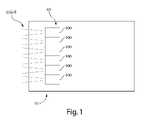
- FIG. 1is a schematic representation of a light-emitting system 50 that has an array 60 of LEDs 100 incorporated therein.
- Array 60is configured so that, during use, light that emerges from LEDs 100 emerges from system 50 .
- light-emitting systemsinclude projectors (e.g., rear projection projectors, front projection projectors), portable electronic devices (e.g., cell phones, personal digital assistants, laptop computers), computer monitors, large area signage (e.g., highway signage), vehicle interior lighting (e.g., dashboard lighting), vehicle exterior lighting (e.g., vehicle headlights, including color changeable headlights), general lighting (e.g., office overhead lighting), high brightness lighting (e.g., streetlights), camera flashes, medical devices (e.g., endoscopes), telecommunications (e.g. plastic fibers for short range data transfer), security sensing (e.g.
- projectorse.g., rear projection projectors, front projection projectors
- portable electronic devicese.g., cell phones, personal digital assistants, laptop computers
- computer monitorslarge area signage (e.g., highway signage), vehicle interior lighting (e.g., dashboard lighting), vehicle exterior lighting (e.g., vehicle headlights, including
- biometricsbiometrics
- integrated optoelectronicse.g., intrachip and interchip optical interconnects and optical clocking
- military field communicationse.g., point to point communications
- biosensinge.g. photo-detection of organic or inorganic substances
- photodynamic therapye.g. skin treatment
- night-vision gogglessolar powered transit lighting, emergency lighting, airport runway lighting, airline lighting, surgical goggles, wearable light sources (e.g. life-vests).
- An example of a rear projection projectoris a rear projector television.
- An example of a front projection projectoris a projector for displaying on a surface, such as a screen or a wall.
- a laptop computercan include a front projection projector.
- LEDs 100can be configured differently.
- system 50includes a single LED 100 .
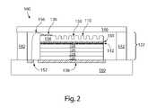
- FIG. 2shows a side view of an LED 100 in the form of a packaged die.
- LED 100includes a multi-layer stack 122 disposed on a submount 120 .
- Multi-layer stack 122includes a 320 nm thick silicon doped (n-doped) GaN layer 134 having a pattern of openings 150 in its upper surface 110 .
- Multi-layer stack 122also includes a bonding layer 124 , a 100 nm thick silver layer 126 , a 40 nm thick magnesium doped (p-doped) GaN layer 128 , a 120 nm thick light-generating region 130 formed of multiple InGaN/GaN quantum wells, and a AlGaN layer 132 .
- n-side contact pad 136is disposed on layer 134 .
- Packaged LED 100also includes a package substrate 150 and metallized portions 152 and 138 supported by substrate 150 .
- Metallized portion 152is electrically connected to n-side contact 136 using a connector 156 , for example, a wire bond.
- Metallized portion 138is in electrical contact with conductive submount 120 and forms an electrical current path to p-doped layer 128 .
- a frame 142is supported by substrate 150 .
- Frame 142supports a transparent cover 140 .
- transparent cover 140is formed of a material that transmits at least about 60% (e.g., at least about 70%, at least about 80%, at least about 90%, at least about 95%) of the light that emerges from LED 100 and impinges on transparent cover 140 .
- Lightis generated by LED 100 as follows.
- P-side contact 138is held at a positive potential relative to n-side contact 136 , which causes electrical current to be injected into LED 100 .
- As the electrical current passes through light-generating region 130electrons from n-doped layer 134 combine in region 130 with holes from p-doped layer 128 , which causes region 130 to generate light.
- Light-generating region 130contains a multitude of point dipole radiation sources that emit light (e.g., isotropically) within region 130 with a spectrum of wavelengths characteristic of the material from which light-generating region 130 is formed.
- the spectrum of wavelengths of light generated by region 130can have a peak wavelength of about 445 nanometers (nm) and a full width at half maximum (FWHM) of about 30 nm.
- the charge carriers in p-doped layer 126have relatively low mobility compared to the charge carriers in the n-doped semiconductor layer 134 .
- placing silver layer 126 (which is conductive) along the surface of p-doped layer 128can enhance the uniformity of charge injection from contact 138 into p-doped layer 128 and light-generating region 130 . This can also reduce the electrical resistance of device 100 and/or increase the injection efficiency of device 100 .
- Because of the relatively high charge carrier mobility of the n-doped layer 134electrons can spread relatively quickly from n-side contact pad 136 throughout layer 134 , so that the current density within light-generating region 130 is substantially uniform across region 130 .
- silver layer 126has relatively high thermal conductivity, allowing layer 126 to act as a heat sink for LED 100 (to transfer heat vertically from multi-layer stack 122 to submount 120 ).
- At least some of the light that is generated by region 130is directed toward silver layer 126 .
- This lightcan be reflected by layer 126 and emerge from LED 100 via surface 110 , or can be reflected by layer 126 and then absorbed within the semiconductor material in LED 100 to produce an electron-hole pair that can combine in region 130 , causing region 130 to generate light.
- at least some of the light that is generated by region 130is directed toward pad 136 .
- the underside of pad 136is formed of a material (e.g., a Ti/Al/Ni/Au alloy) that can reflect at least some of the light generated by light-generating region 130 .
- the light that is directed to pad 136can be reflected by pad 136 and subsequently emerge from LED 100 via surface 110 (e.g., by being reflected from silver layer 126 ), or the light that is directed to pad 136 can be reflected by pad 136 and then absorbed within the semiconductor material in LED 100 to produce an electron-hole pair that can combine in region 130 , causing region 130 to generate light (e.g., with or without being reflected by silver layer 126 ).
- surface 110 of LED 100is not flat but consists of a pattern of openings 150 .
- various valuescan be selected for the depth of openings 150 , the diameter of openings 150 and the spacing between nearest neighbors in openings 150 can vary.
- Examples of patterns transferred into the surfaceinclude a variety of patterns that can increase extraction efficiency from the light emitting device. For example, patterns having a detuned quasicrystalline or complex periodic structures, periodic patterns, and non-periodic patterns. Such patterns are disclosed, for example, in application Ser. No. 10/724,004, filed Sep. 26, 2003 which is hereby incorporated by reference.
- a complex periodic patternis a pattern that has more than one feature in each unit cell that repeats in a periodic fashion.
- a nonperiodic patternis a pattern that has no translational symmetry over a unit cell that has a length that is at least 50 times the peak wavelength of light generated by region 130 .
- nonperiodic patternsinclude aperiodic patterns, quasicrystalline patterns, Robinson patterns, and Amman patterns.
- a detuned patternis a pattern with nearest neighbors in the pattern have a center-to-center distance with a value between (a ⁇ a) and (a+ ⁇ a), where “a” is the lattice constant for the pattern and “ ⁇ a” is a detuning parameter with dimensions of length and where the detuning can occur in random directions.
- detuning parameter, ⁇ ais generally at least about one percent (e.g., at least about two percent, at least about three percent, at least about four percent, at least about five percent) of ideal lattice constant, a, and/or at most about 25% (e.g., at most about 20%, at most about 15%, at most about 10%) of ideal lattice constant, a.
- the nearest neighbor spacingsvary substantially randomly between (a ⁇ a) and (a+ ⁇ a), such that the pattern is substantially randomly detuned.
- FIGS. 3A and 3Bshow a top view and side view of an LED 174 in the form of a packaged die 170 .
- the packageincludes a substrate 172 that supports LED 174 .
- the packagealso includes a frame 176 and a transparent cover 178 supported by frame 176 .
- transparent cover 178is formed of a material that transmits at least about 60% (e.g., at least about 70%, at least about 80%, at least about 90%, at least about 95%) of the light that emerges from LED 174 and impinges on transparent cover 178 .
- Examples of materials from which transparent cover 178 can be formedinclude glass, silica, quartz, plastic, and polymers.
- the packageshould be capable of transmitting light while also providing mechanical and environmental protection of LED 174 and allowing heat generated in LED 174 to be dissipated.
- transparent cover 178can be coated with one or more anti-reflection coatings to increase light transmission.
- additional optical componentscan be included in or supported by transparent cover 178 . Examples of such optical components include lenses, mirrors, reflectors, collimators, beam splitters, beam combiners, dichroic mirrors, filters, polarizers, polarizing beam splitters, prisms, total internal reflection prisms, optical fibers, light guides and beam homogenizers.
- transparent cover 178is disposed in close proximity to an upper surface 175 of LED 174 .
- a spacing 190 between upper surface 175 of LED 174 and a lower surface 173 of transparent cover 178 nearest to upper surface 175 of LED 174can be relatively small.
- spacing 190can be from about one micron to about 500 microns (e.g., at most about 500 microns, at most about 400 microns, at most about 300 microns, at most about 250 microns, at most about 200 microns, at most about 150 microns, at most about 100 microns, at most about 50 microns, at most about 25 microns).
- transparent cover 178is disposed in contact with at least a portion of upper surface 175 of LED 174 .
- a cross-sectional area of LED 174can be relatively large.
- length 180 or width 182 of LED 174can be at least about one millimeter (e.g., at least about two millimeters, at least about three millimeters, at least about five millimeters, at least about ten millimeters). It can be desirable for spacing 190 between surface 175 of LED 174 and surface 173 of transparent cover 178 to be proportional to the length 180 or width 182 of LED 174 .
- a ratio of length 180 or width 182 of LED 174 to spacing 190can be at least about five (e.g., at least about five at least about seven, at least about ten, at least about fifteen, at least about twenty, at least about thirty, at least about fifty, at least about seventy-five, at least about one-hundred, at least about two-hundred).
- FIGS. 4A and 4Bshow a side view and top view of an LED 216 in the form of a packaged die 200 .
- the packageincludes a transparent cover 202 , a support 208 , conductive pads 210 , and a substrate 218 .
- LED 216is attached to substrate 218 using a solder layer 214 (examples of solder include AuSn solder, PbSn solder, NiSn solder, InSn solder, InAgSn solder, and PbSnAg solder) or using an electrically conductive epoxy (e.g., silver filled epoxy).
- packaged die 200can include a thermal pad or other heat dissipation layer 212 (e.g., a silver layer, a copper layer). Heat dissipation layer 212 can have a relatively high thermal conductivity, allowing layer 212 to act as a heat sink for LED 216 (e.g., to transfer heat vertically from LED 216 to substrate 218 ).
- Package 200is designed to allow electrical current to flow from a pad 210 to a surface 203 of LED 216 .
- Pad 210is electrically connected to a conductive support 208 such as a metal post.
- conductive supports 208also provide physical support for a cover 202 .
- Conductive supports 208can be constructed in a variety of ways. For example, conductive supports 208 could be constructed by metal plating, solder ball, clips, or by a prefabricated frame.
- Transparent cover 202can be pre-patterned with metal contacts 206 . Contacts 206 on transparent cover 202 are electrically connected to pads 210 via conductive supports 208 . Contacts 206 can be composed of a variety of materials.
- contacts 206can be composed of Cu, Ag, Au or blanket transparent metal such as ITO, Au, AuNi.
- Transparent cover 202is adhered to LED 216 via solder 204 (e.g., AgSn solder, Au—Sn solder, Pb—Sn solder, Pd—In solder, or Au—Ge solder) forming an electrical current path between contacts 207 on surface 203 of LED 216 and contacts 206 on transparent cover 202 .
- Conductive pads 207allow current to be spread to the LED surface 203 . While FIGS. 4A and 4B show two pads 210 , other arrangements are possible.
- package 200could include a single pad 210 or more than two pads (e.g., three pads, four pads, five pads, six pads).
- FIGS. 5A and 5Bshow a side view and top view of an LED 216 in the form of a packaged device 230 .
- the packaged device 230includes a transparent cover 202 , a conductive connection 238 , conductive pads 210 , and a substrate 218 .
- LED 216can be disposed within the package and can be attached to substrate 218 as described above in relation to FIGS. 4A and 4B .
- Package 230is designed to allow electrical current to flow from a pad 210 to a surface 203 of LED 216 .
- Pad 210is electrically connected to a using a conductive connection 238 such as a metal spring or clip.
- the metal spring or clipcan be composed of a semi-flexible material such that the spring or clip can be bent to allow for differing thicknesses of LED 216 .
- conductive connection 238can be made of conductive materials such as gold, aluminum, silver, platinum, copper, and other metals or metal alloys.
- Transparent cover 202can be pre-patterned with metal contacts 206 . Contacts 206 on transparent cover 202 are electrically connected to pads 210 via conductive connection 238 . Contacts 206 can be composed of a variety of materials.
- contacts 206can be composed of Cu, Ag, Au or blanket transparent metal such as ITO, Au, AuNi.
- Transparent cover 202is adhered to LED 216 via solder 204 (e.g., AgSn solder, Au—Sn solder, Pb—Sn solder, Pd—In solder, or Au—Ge solder) forming an electrical current path between contacts 207 on surface 203 of LED 216 and contacts 206 on transparent cover 202 .
- Conductive pads 207allow current to be spread to the LED surface 203 . While FIGS. 5A and 5B show two pads 210 , other arrangements are possible.
- package 230could include a single pad or more than two pads (e.g., three pads, four pads, five pads, six pads).
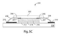
- FIG. 5Cshows a side view and top view of an LED 216 in the form of a packaged device 231 .
- the packaged device 230includes a transparent cover 202 , a conductive connection 238 , conductive pads 210 , and a substrate 218 .
- LED 216can be disposed within the package and can be attached to substrate 218 as described above in relation to FIGS. 5A and 5B .
- Package 230is designed to allow electrical current to flow from a pad 210 to a surface 203 of LED 216 .
- Pad 210is electrically connected to a using a conductive connection 238 as described above.
- Transparent cover 202can be pre-patterned with metal contacts 206 .
- Contacts 206 on transparent cover 202are electrically connected to contacts 207 on surface 203 of LED 216 .
- contacts 206 on transparent cover 202can be in direct contact with contacts 207 on surface 203 of LED 216 forming an electrical current path between contacts 207 on surface 203 of LED 216 and contacts 206 on transparent cover 202 .
- one or both of contacts 206 and 207may have a roughened surface. It is believed that roughening the surface of one or both of contacts 206 and 207 can facilitate the current flow between contacts 206 and 207 .
- FIGS. 6A and 6Bshow a side view and top view of an LED 216 in the form of a packaged device 250 that includes contacts 258 and a transparent cover 252 having a recessed region 253 .
- LED 216can be attached to a package substrate 218 as described above in relation to FIGS. 4A and 4B .
- Packaged device 250includes a transparent cover 252 that is self supporting.
- Transparent cover 252includes a region 251 about parallel to the surface of LED 216 through which light from LED 216 emerges and support regions 254 about perpendicular to the about parallel region 251 forming a recessed region 253 in transparent cover 252 .
- a recess depth 255 of recess region 253can be equal to or slightly larger than thicknesses 257 of LED 216 , heat dissipation layer 212 , and solder layer 214 combined.
- recess depth 255can be from about five microns to about 400 microns greater than thicknesses 257 .
- Package 250is designed to allow electrical current to flow from a pad 210 to a surface 203 of LED 216 .
- Pad 210is electrically connected to conductive contacts 258 on transparent cover 252 .
- the conductive contacts 258extend along regions 254 of transparent cover 232 and a portion of region 251 of transparent cover 252 .
- Transparent cover 252is aligned such that the conductive contacts 258 are aligned with metal contact pads 207 on the surface of LED 216 .
- a conductive adhesive 204e.g., solder, metal filled epoxy
- FIGS. 7A and 7Bshow a side view and top view of an LED 216 in the form of a packaged device 270 .
- Packaged device 270includes a recessed transparent cover 272 as described above in relation to FIGS. 6A and 6B .
- Packaged device 270also includes a substrate 278 having etched regions 280 and 282 that provide self-alignment of LED 216 and transparent cover 272 .
- Etched region 282is slightly larger than the size of LED 216 and LED 216 is disposed in etched region 282 .
- Etched region 280provides alignment for transparent cover 272 .
- Etched region 280can include a metal contact layer 286 disposed in the bottom of etched region 280 .
- Etched region 280aligns transparent cover 272 with LED 216 .
- a packaged LED 300includes LED 216 , a substrate 218 , an insulating layer 308 , conductive contacts 306 , and a transparent cover 302 .
- Package 300is designed to allow electrical current to flow from a portion 309 of conductive contacts 306 disposed on substrate 218 to a surface 203 of LED 216 .
- Insulating layer 308is disposed on a portion of the top surface 203 and sidewalls of LED 216 and conductive contacts 306 are disposed on insulating layer 308 .
- conductive contacts 306can be formed on the surface of the insulating layer 308 to provide an electrical connection between contact 207 on the surface of LED 216 and portion 309 of conductive contacts 306 .
- Transparent cover 302can be supported by conductive contacts 306 and provides physical protection for LED 216 .
- multiple LEDscan be arranged to form an array of LEDs.
- multiple individual LEDscan be packed closely together in an array. Closely packing multiple LEDs to form an array can provide various advantages. For example, if one LED does not function (e.g., due to a defect or malfunction), the failure of the LED does not significantly diminish the performance of the array because the individual devices are closely packed. Closely packing LEDs can increase light output for a given array area by reducing the spacing between the LEDs.
- the number of LEDs and the placement of each LED in the array of LEDscan be selected as desired.
- FIGS. 9 , 10 , 11 , and 12show exemplary light emitting device (LED) die orientations for multi-chip arrays.
- FIG. 9shows an array 350 of light emitting devices that includes two LEDs 352 and 354 arranged in a single row.
- FIG. 10shows an array 360 of light emitting devices that includes four LEDs 362 , 364 , 366 , and 368 arranged in a 2 ⁇ 2 matrix (i.e., arranged in two rows and two columns).
- FIG. 9shows an array 350 of light emitting devices that includes two LEDs 352 and 354 arranged in a single row.
- FIG. 10shows an array 360 of light emitting devices that includes four LEDs 362 , 364 , 366 , and 368 arranged in a 2 ⁇ 2 matrix (i.e., arranged in two rows and two columns).
- FIG. 9shows an array 350 of light emitting devices that includes two LEDs 352 and 354 arranged in a single row.
- FIG. 10shows an array
- FIG. 11shows an array 380 of light emitting devices that includes nine LEDs 382 , 383 , 384 , 385 , 386 , 387 , 388 , 389 , 390 , 391 , 392 , and 393 arranged in a 3 ⁇ 4 matrix (i.e., arranged in three rows and four columns).
- the number of rows and columns in the matrix of LEDscan be selected as desired. For example, FIG.
- N rowse.g., a first row 408 , a second row 410 , and an N th row 412
- M columnse.g., a first column 402 , a second column 404 , and an M th column 406
- N and Mare both positive integers.
- the number of LEDs and the placement of each LED in the multi-chip arraycan be selected to form a desired aspect ratio (as defined by the length 414 of array 400 to the width 416 of array 400 ).
- the aspect ratio of array 400can be, for example, 16 ⁇ 9, 4 ⁇ 3, 1920 ⁇ 1080, 640 ⁇ 480, 800 ⁇ 600, 1024 ⁇ 700, 1024 ⁇ 768, 1024 ⁇ 720, 1280 ⁇ 720, 1280 ⁇ 768, 1280 ⁇ 960, or 1280 ⁇ 1064.
- a desired aspect ratiocan be obtained by appropriately sizing and/or spacing LED die.
- multiple LEDscan be packed closely together in an array. As shown in FIG. 13 multiple LEDs 424 , 426 , 428 , and 430 are supported by a substrate 422 . The LEDs can be positioned on substrate 422 to reduce or minimize the spacing between adjacent LEDs.
- LEDs 424 , 426 , 428 , and 430can be arranged such that a spacing between the nearest edges of neighboring die in the array of LEDs (e.g., spacing 436 and/or spacing 438 ) is relatively small.
- spacing 436 or 438can be at most about 250 microns (e.g., at most about 200 microns, at most about 150 microns, at most about 100 microns, at most about 75 microns, at most about 50 microns).
- LEDs 424 , 426 , 428 , and 430can be arranged on substrate 422 to reduce or minimize the amount of surface area disposed between LEDs 424 , 426 , 428 , and 430 (as indicated by area 434 ).
- a total area of the LED arraycan be defined by the area enclosed by an outer perimeter of the LEDs (e.g., as indicated by dashed line 432 ).
- a total surface area of the LEDscan be about equal to the sum of the area of each LED in the array of LEDs (e.g., a sum of the area of LEDs 424 , 426 , 428 , and 430 ).
- the LEDs in the array of light emitting devicescan be positioned such that a ratio of a sum of a total area of all of the light emitting devices (e.g., a sum of the areas LEDs 424 , 426 , 428 , and 430 ) in the array to the total area 432 can be at least about 0.8 (e.g., at least about 0.85, at least about 0.9, at least about 0.95). In some embodiments, ratio of a sum of a total area of all of the light emitting devices in the array to the total area 432 can be at least about 0.5 (e.g., at least about 0.6, at least about 0.7).
- an electrical contact to the n-doped or p-doped layer of the LEDis formed through a conductive substrate or submount.
- the conductive substrate or submountis attached to conductive contact pads supported by the package, for example, using a conductive paste (e.g., a metal filled paste), solder, or conductive tape.
- spacing 438 or 436can be limited by the spread of the material used to attach the LED to the substrate or submount into surrounding areas which can cause an electrical short between the die.
- Various approachescan be used to minimize the spread of the die attach material.
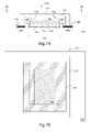
- FIGS. 14A-14Cshow an exemplary process for attaching an LED die 440 to a package substrate 442 using a layer of die attach material 441 .
- the die attach material 441is deposited on package substrate 442 in a location corresponding to a desired placement of the die 440 .
- the area coverage of die attach material 441is less than the area of die 440 such that a portion 439 of the LED is not initially in contact with the die attach material (as shown in FIGS. 14A and 14B ).
- FIG. 14Cwhen pressure and/or heat are applied to the LED and/or the package substrate (as indicated by arrows 443 ) the die attach material 441 spreads laterally as indicated by arrows 444 . Because die attach material 441 did not extend to the edge of the die prior to the application of pressure and heat, the die attach material can spread laterally and be contained in an area of the substrate 442 disposed under die 440 .
- FIGS. 15-17show exemplary embodiments where spreading of the die attach material 441 is controlled by patterning an underside of the die (e.g., underside 447 of die 445 or underside 448 of die 446 ).
- the underside 447 or 448is patterned with grooves 481 and 483 that collect excess attach material 441 as the material spreads due to the application of heat and/or pressure.
- FIG. 17shows an exemplary embodiment where ridges 449 are patterned into the underside 451 of a die 447 . Ridges 449 form a barrier to the spreading of die attach material 441 .
- FIGS. 14-17show a single die attached to a substrate using a die attach material
- multiple diecould be attached to the substrate using the die attach material.
- attaching the die using the arrangements shown in FIGS. 14-17allows multiple die to be closely spaced on a substrate without shorting the die.
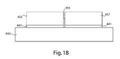
- FIG. 18shows an exemplary embodiment in which an insulating region 455 is disposed between LED 453 and LED 455 .
- the insulating region 455is supported by a substrate 442 and controls the spreading of the die attach material 441 .
- the insulating region 455forms a barrier that limits spreading.
- the insulating region 455can also aid in assembly and alignment of LEDS 453 and 457 .
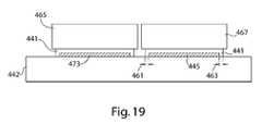
- FIG. 19shows a layer 473 supported by a package substrate 442 which can control the lateral spreading of the die attach material 441 .
- Layer 473can be formed of a rigid or semi-rigid material that does not flow with the application of heat and pressure typical for bonding the LEDs 465 and 467 to substrate 442 .
- the area coverage of layer 473is less than the area of LEDs 465 and 467 such that a portion 463 of the LED extends past the patterned region 473 .
- pressure and heatare applied to the LED and/or the package substrate the die attach material 441 spreads laterally.
- the area of layer 473is smaller than the area of LEDs 465 and 467 , the excess die attach material 441 spreads over the edges of the layer 473 (as indicated by region 461 ).
- the area of layer 473can be selected to be sufficiently smaller than the area of the LED such that the lateral spreading of die attach material 441 can be limited to a region of the substrate 442 under the die.
- FIGS. 20A and 20Bshow an exemplary a package 450 including an array of four LEDs 452 , 454 , 456 , and 458 arranged in a two by two matrix.
- the packageincludes a package substrate 460 (e.g., a board composed of AlN, Cu), n-contact leads 462 and 464 and p-contact leads 468 , 470 , 472 , and 474 .
- the contact leadsinclude solder pads 476 , 478 , 480 , 482 , 484 , 486 , 490 , 492 , and 494 for external wiring.
- n-contacts for LEDs 452 and 456are connected and n-contacts for LEDs 454 and 458 are connected.
- vertical dieare connected in parallel (shown schematically in FIG. 20B ).
- LEDsmay or may not be encapsulated.
- An optional window(not shown) can cover all, some, or one of the die(s) on substrate 460 .
- a window or encapsulationcan include additional optics, e.g., patterning, filters, phosphor, lenses, openings, and the like. While FIG. 20A shows a schematic representation of an array of LEDs 452 , 454 , 456 , and 458 where the vertical die are connected in parallel, in some embodiments LEDs 452 , 454 , 456 , and 458 are not in parallel, but are each individually addressed.
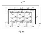
- FIG. 21shows an exemplary a package 480 including an array of six LEDs 482 , 484 , 486 , 488 , 490 , and 492 supported by a package substrate 481 and arranged in a two by three matrix.
- the array of LED diecan be arranged such that the combined emission area forms a desired aspect ratio.
- LEDs 482 , 484 , 486 , 488 , 490 , and 492are connected in series.
- N-contact pads 494 , 496 , 498 , 500 , 502 , and 504can be electrically connected to a network of contacts lines or fingers that extend over the surface of LEDs 482 , 484 , 486 , 488 , 490 , and 492 to facilitate better current spreading.
- n-pads 494 , 496 , 498 , 500 , 502 , and 504are connected (e.g., via wirebonding, patterned interconnects, metallized window) to p-contact pads 506 , 508 , 510 , 512 , 514 , and 516 which access a p-doped region on an under side of the device.
- package 480also includes a transparent cover 520 supported by a frame 522 (e.g., as described above).
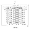
- FIG. 22shows an exemplary a die layout 540 including an array of six LEDs 542 , 544 , 546 , 548 , 550 , and 552 supported by a package substrate 554 and arranged in a one by six matrix. LEDs 542 , 544 , 546 , 548 , 550 , and 552 are connected in series.
- n-pads 556 , 558 , 560 , 562 , 564 , and 566are connected (e.g., via wirebonding, patterned interconnects, metallized window) to p-contact pads 568 , 570 , 572 , 574 , 576 and 578 which access a p-doped region on an under side of LEDs 542 , 544 , 546 , 548 , 550 , and 552 respectively.
- the transparent covercan be patterned and/or contain optical components, for example, PL, color filter(s), polarization, phosphor layer(s), and ARC.
- a windowis made of a transparent material which is thermally conductive (e.g., diamond, sapphire)
- the packagecan include a heat transfer interface.
- a heat transfer interfacecould incorporate pattering (mesas, groves) to increase thermal contact and reduce voids during adhesion.
- the packagescan be mounted to core board and may or may not include heat extraction device (e.g., an additional heat-sink, a thermoelectric cooler, fluid convection tubes, and the like).
- heat extraction devicee.g., an additional heat-sink, a thermoelectric cooler, fluid convection tubes, and the like.
Landscapes
- Engineering & Computer Science (AREA)
- Microelectronics & Electronic Packaging (AREA)
- Computer Hardware Design (AREA)
- Power Engineering (AREA)
- Physics & Mathematics (AREA)
- Optics & Photonics (AREA)
- General Engineering & Computer Science (AREA)
- Led Device Packages (AREA)
- Packages (AREA)
Abstract
Description
Claims (14)
Priority Applications (5)
| Application Number | Priority Date | Filing Date | Title |
|---|---|---|---|
| US11/210,013US7692207B2 (en) | 2005-01-21 | 2005-08-23 | Packaging designs for LEDs |
| PCT/US2006/001054WO2006078530A2 (en) | 2005-01-21 | 2006-01-12 | Packaging designs for leds |
| TW100104726ATW201125159A (en) | 2005-01-21 | 2006-01-17 | Packaging designs for LEDs |
| TW095101693ATWI356506B (en) | 2005-01-21 | 2006-01-17 | Light-emitting system |
| TW100104727ATW201125160A (en) | 2005-01-21 | 2006-01-17 | Packaging designs for LEDs |
Applications Claiming Priority (5)
| Application Number | Priority Date | Filing Date | Title |
|---|---|---|---|
| US64572105P | 2005-01-21 | 2005-01-21 | |
| US64572005P | 2005-01-21 | 2005-01-21 | |
| US65986105P | 2005-03-08 | 2005-03-08 | |
| US66092105P | 2005-03-11 | 2005-03-11 | |
| US11/210,013US7692207B2 (en) | 2005-01-21 | 2005-08-23 | Packaging designs for LEDs |
Publications (2)
| Publication Number | Publication Date |
|---|---|
| US20060163590A1 US20060163590A1 (en) | 2006-07-27 |
| US7692207B2true US7692207B2 (en) | 2010-04-06 |
Family
ID=36692734
Family Applications (1)
| Application Number | Title | Priority Date | Filing Date |
|---|---|---|---|
| US11/210,013Active2028-02-06US7692207B2 (en) | 2005-01-21 | 2005-08-23 | Packaging designs for LEDs |
Country Status (2)
| Country | Link |
|---|---|
| US (1) | US7692207B2 (en) |
| WO (1) | WO2006078530A2 (en) |
Cited By (16)
| Publication number | Priority date | Publication date | Assignee | Title |
|---|---|---|---|---|
| US20080067533A1 (en)* | 2006-09-14 | 2008-03-20 | Luminus Devices, Inc. | Flexible circuit light-emitting structures |
| US20090218588A1 (en)* | 2007-12-06 | 2009-09-03 | Paul Panaccione | Chip-scale packaged light-emitting devices |
| US20100059772A1 (en)* | 2006-03-30 | 2010-03-11 | Sumitomo Chemical Company, Limited | Light Emitting Device |
| US20100149815A1 (en)* | 2008-10-17 | 2010-06-17 | Luminus Devices, Inc. | Remote lighting assemblies and methods |
| US20110084292A1 (en)* | 2009-10-01 | 2011-04-14 | Luminus Devices, Inc. | Arrays of light emitting devices |
| US20110121347A1 (en)* | 2009-11-24 | 2011-05-26 | Luminus Devices, Inc. | Systems and methods for managing heat from an led |
| US20110121726A1 (en)* | 2009-11-23 | 2011-05-26 | Luminus Devices, Inc. | Solid-state lamp |
| US20110233583A1 (en)* | 2010-03-27 | 2011-09-29 | H&T Electronics Co., Ltd. | High-power led package |
| US20140029275A1 (en)* | 2012-07-24 | 2014-01-30 | Ningbo Yofun Heating Appliance Co., Ltd. | Led mounting assembly |
| US8746923B2 (en) | 2011-12-05 | 2014-06-10 | Cooledge Lighting Inc. | Control of luminous intensity distribution from an array of point light sources |
| US8872217B2 (en) | 2011-04-15 | 2014-10-28 | Luminus Devices, Inc. | Electronic device contact structures |
| US20160049564A1 (en)* | 2014-08-13 | 2016-02-18 | Samsung Electronics Co., Ltd. | Semiconductor device and method of manufacturing the same |
| US9461027B2 (en) | 2012-08-07 | 2016-10-04 | Koninklijke Philips N.V. | LED package and manufacturing method |
| USD777121S1 (en) | 2013-03-05 | 2017-01-24 | Luminus Devices, Inc. | LED package |
| US9627582B2 (en) | 2011-06-28 | 2017-04-18 | Luminus Devices, Inc. | Light-emitting diode architectures for enhanced performance |
| DE102021100530A1 (en) | 2021-01-13 | 2022-07-14 | OSRAM Opto Semiconductors Gesellschaft mit beschränkter Haftung | OPTOELECTRONIC SEMICONDUCTOR DEVICE AND METHOD FOR MANUFACTURING AN OPTOELECTRONIC SEMICONDUCTOR DEVICE |
Families Citing this family (27)
| Publication number | Priority date | Publication date | Assignee | Title |
|---|---|---|---|---|
| US7692207B2 (en) | 2005-01-21 | 2010-04-06 | Luminus Devices, Inc. | Packaging designs for LEDs |
| US7170100B2 (en)* | 2005-01-21 | 2007-01-30 | Luminus Devices, Inc. | Packaging designs for LEDs |
| US7683475B2 (en)* | 2006-03-31 | 2010-03-23 | Dicon Fiberoptics, Inc. | LED chip array module |
| US8643195B2 (en)* | 2006-06-30 | 2014-02-04 | Cree, Inc. | Nickel tin bonding system for semiconductor wafers and devices |
| US7910945B2 (en)* | 2006-06-30 | 2011-03-22 | Cree, Inc. | Nickel tin bonding system with barrier layer for semiconductor wafers and devices |
| JP2009545894A (en)* | 2006-07-31 | 2009-12-24 | スリーエム イノベイティブ プロパティズ カンパニー | LED source with hollow condenser lens |
| US20080036972A1 (en)* | 2006-07-31 | 2008-02-14 | 3M Innovative Properties Company | Led mosaic |
| EP2049947A1 (en) | 2006-07-31 | 2009-04-22 | 3M Innovative Properties Company | Optical projection subsystem |
| US8075140B2 (en)* | 2006-07-31 | 2011-12-13 | 3M Innovative Properties Company | LED illumination system with polarization recycling |
| US20080051135A1 (en)* | 2006-07-31 | 2008-02-28 | 3M Innovative Properties Company | Combination camera/projector system |
| US7855459B2 (en)* | 2006-09-22 | 2010-12-21 | Cree, Inc. | Modified gold-tin system with increased melting temperature for wafer bonding |
| US8179034B2 (en) | 2007-07-13 | 2012-05-15 | 3M Innovative Properties Company | Light extraction film for organic light emitting diode display and lighting devices |
| US20100038670A1 (en)* | 2008-08-18 | 2010-02-18 | Luminus Devices, Inc. | Illumination assembly including chip-scale packaged light-emitting device |
| WO2010022102A2 (en)* | 2008-08-19 | 2010-02-25 | Plextronics, Inc. | User configurable mosaic light emitting apparatus |
| US9142714B2 (en) | 2008-10-09 | 2015-09-22 | Nitek, Inc. | High power ultraviolet light emitting diode with superlattice |
| KR20110105867A (en)* | 2009-01-21 | 2011-09-27 | 코닌클리케 필립스 일렉트로닉스 엔.브이. | A light source comprising a light recycling device and a corresponding light recycling device |
| DE102009051129A1 (en) | 2009-10-28 | 2011-06-01 | Osram Opto Semiconductors Gmbh | Optoelectronic component and method for producing an optoelectronic component |
| EP2641014A4 (en)* | 2010-11-16 | 2014-07-02 | Holding Llc Photon | Systems, methods and/or devices for providing led lighting |
| KR101880132B1 (en)* | 2011-08-17 | 2018-07-19 | 엘지이노텍 주식회사 | Light emitting moudule |
| US9169988B2 (en)* | 2011-08-02 | 2015-10-27 | Lg Innotek Co., Ltd. | Light emitting module and head lamp including the same |
| WO2014157455A1 (en) | 2013-03-28 | 2014-10-02 | 東芝ホクト電子株式会社 | Light-emitting device, production method therefor, and device using light-emitting device |
| JP6244784B2 (en)* | 2013-09-30 | 2017-12-13 | 日亜化学工業株式会社 | Light emitting device |
| US20150290473A1 (en)* | 2014-04-11 | 2015-10-15 | Elekta Ab (Publ) | Radiotherapy system |
| KR20150122360A (en)* | 2014-04-23 | 2015-11-02 | (주)라이타이저코리아 | Package for Light Emitting Device and Method for Manufacturing thereof |
| JP6789970B2 (en)* | 2015-03-30 | 2020-11-25 | ルミレッズ ホールディング ベーフェー | Peripheral heat sink device for high brightness light emitting devices |
| EP3547360A1 (en)* | 2018-03-29 | 2019-10-02 | Siemens Aktiengesellschaft | Semiconductor module and method of manufacturing same |
| JP7556375B2 (en)* | 2022-04-20 | 2024-09-26 | トヨタ自動車株式会社 | Vehicle interior lighting system |
Citations (91)
| Publication number | Priority date | Publication date | Assignee | Title |
|---|---|---|---|---|
| US3293513A (en) | 1962-08-08 | 1966-12-20 | Texas Instruments Inc | Semiconductor radiant diode |
| US3922706A (en) | 1965-07-31 | 1975-11-25 | Telefunken Patent | Transistor having emitter with high circumference-surface area ratio |
| US4864370A (en) | 1987-11-16 | 1989-09-05 | Motorola, Inc. | Electrical contact for an LED |
| US5126231A (en) | 1990-02-26 | 1992-06-30 | Applied Materials, Inc. | Process for multi-layer photoresist etching with minimal feature undercut and unchanging photoresist load during etch |
| US5132751A (en) | 1990-06-08 | 1992-07-21 | Eastman Kodak Company | Light-emitting diode array with projections |
| US5162878A (en) | 1991-02-20 | 1992-11-10 | Eastman Kodak Company | Light-emitting diode array with projections |
| US5359345A (en) | 1992-08-05 | 1994-10-25 | Cree Research, Inc. | Shuttered and cycled light emitting diode display and method of producing the same |
| US5363009A (en) | 1992-08-10 | 1994-11-08 | Mark Monto | Incandescent light with parallel grooves encompassing a bulbous portion |
| US5426657A (en) | 1993-03-04 | 1995-06-20 | At&T Corp. | Article comprising a focusing semiconductor laser |
| US5491350A (en) | 1993-06-30 | 1996-02-13 | Hitachi Cable Ltd. | Light emitting diode and process for fabricating the same |
| US5631190A (en) | 1994-10-07 | 1997-05-20 | Cree Research, Inc. | Method for producing high efficiency light-emitting diodes and resulting diode structures |
| US5633527A (en) | 1995-02-06 | 1997-05-27 | Sandia Corporation | Unitary lens semiconductor device |
| US5724062A (en) | 1992-08-05 | 1998-03-03 | Cree Research, Inc. | High resolution, high brightness light emitting diode display and method and producing the same |
| WO1998014986A1 (en) | 1996-10-01 | 1998-04-09 | Siemens Aktiengesellschaft | Method for separating two material layers and electronic components produced therewith |
| US5779924A (en) | 1996-03-22 | 1998-07-14 | Hewlett-Packard Company | Ordered interface texturing for a light emitting device |
| US5814839A (en) | 1995-02-16 | 1998-09-29 | Sharp Kabushiki Kaisha | Semiconductor light-emitting device having a current adjusting layer and a uneven shape light emitting region, and method for producing same |
| US5834331A (en) | 1996-10-17 | 1998-11-10 | Northwestern University | Method for making III-Nitride laser and detection device |
| US5955749A (en) | 1996-12-02 | 1999-09-21 | Massachusetts Institute Of Technology | Light emitting device utilizing a periodic dielectric structure |
| US6072628A (en) | 1997-01-29 | 2000-06-06 | Thomson Multimedia S.A. | Optical polarisation device |
| US6071795A (en) | 1998-01-23 | 2000-06-06 | The Regents Of The University Of California | Separation of thin films from transparent substrates by selective optical processing |
| US6091085A (en) | 1998-02-19 | 2000-07-18 | Agilent Technologies, Inc. | GaN LEDs with improved output coupling efficiency |
| US6122103A (en) | 1999-06-22 | 2000-09-19 | Moxtech | Broadband wire grid polarizer for the visible spectrum |
| US6222207B1 (en) | 1999-05-24 | 2001-04-24 | Lumileds Lighting, U.S. Llc | Diffusion barrier for increased mirror reflectivity in reflective solderable contacts on high power LED chip |
| US6265820B1 (en) | 1998-01-29 | 2001-07-24 | Emagin Corporation | Heat removal system for use in organic light emitting diode displays having high brightness |
| US6287882B1 (en) | 1999-10-04 | 2001-09-11 | Visual Photonics Epitaxy Co., Ltd. | Light emitting diode with a metal-coated reflective permanent substrate and the method for manufacturing the same |
| US6288840B1 (en) | 1999-06-22 | 2001-09-11 | Moxtek | Imbedded wire grid polarizer for the visible spectrum |
| US6303405B1 (en) | 1998-09-25 | 2001-10-16 | Kabushiki Kaisha Toshiba | Semiconductor light emitting element, and its manufacturing method |
| US6335548B1 (en) | 1999-03-15 | 2002-01-01 | Gentex Corporation | Semiconductor radiation emitter package |
| US6388264B1 (en) | 1997-03-28 | 2002-05-14 | Benedict G Pace | Optocoupler package being hermetically sealed |
| US6410942B1 (en) | 1999-12-03 | 2002-06-25 | Cree Lighting Company | Enhanced light extraction through the use of micro-LED arrays |
| US6426515B2 (en) | 2000-04-21 | 2002-07-30 | Fujitsu Limited | Semiconductor light-emitting device |
| US20020110172A1 (en) | 2000-06-02 | 2002-08-15 | Ghulam Hasnain | Efficiency GaN-based light emitting devices |
| WO2002071450A2 (en) | 2001-03-06 | 2002-09-12 | Emcore Corporation | Led lead for improved light extraction |
| US6465808B2 (en) | 2000-11-24 | 2002-10-15 | Highlink Technology Corporation | Method and structure for forming an electrode on a light emitting device |
| US6469324B1 (en) | 1999-05-25 | 2002-10-22 | Tien Yang Wang | Semiconductor light-emitting device and method for manufacturing the same |
| US6504180B1 (en) | 1998-07-28 | 2003-01-07 | Imec Vzw And Vrije Universiteit | Method of manufacturing surface textured high-efficiency radiating devices and devices obtained therefrom |
| US6522063B2 (en) | 2001-03-28 | 2003-02-18 | Epitech Corporation | Light emitting diode |
| US6534798B1 (en) | 1999-09-08 | 2003-03-18 | California Institute Of Technology | Surface plasmon enhanced light emitting diode and method of operation for the same |
| US6574383B1 (en) | 2001-04-30 | 2003-06-03 | Massachusetts Institute Of Technology | Input light coupler using a pattern of dielectric contrast distributed in at least two dimensions |
| US6573537B1 (en) | 1999-12-22 | 2003-06-03 | Lumileds Lighting, U.S., Llc | Highly reflective ohmic contacts to III-nitride flip-chip LEDs |
| US20030143772A1 (en) | 2002-01-30 | 2003-07-31 | United Epitaxy Co., Ltd. | High efficiency light emitting diode and method of making the same |
| US20030141507A1 (en) | 2002-01-28 | 2003-07-31 | Krames Michael R. | LED efficiency using photonic crystal structure |
| US6642618B2 (en) | 2000-12-21 | 2003-11-04 | Lumileds Lighting U.S., Llc | Light-emitting device and production thereof |
| US6649437B1 (en) | 2002-08-20 | 2003-11-18 | United Epitaxy Company, Ltd. | Method of manufacturing high-power light emitting diodes |
| US6657236B1 (en) | 1999-12-03 | 2003-12-02 | Cree Lighting Company | Enhanced light extraction in LEDs through the use of internal and external optical elements |
| US20030222263A1 (en) | 2002-06-04 | 2003-12-04 | Kopin Corporation | High-efficiency light-emitting diodes |
| US6690268B2 (en) | 2000-03-02 | 2004-02-10 | Donnelly Corporation | Video mirror systems incorporating an accessory module |
| US20040027062A1 (en) | 2001-01-16 | 2004-02-12 | General Electric Company | Organic electroluminescent device with a ceramic output coupler and method of making the same |
| US20040043524A1 (en) | 2002-08-28 | 2004-03-04 | Arima Optoelectronics Corp. | Method for fabricating light emitting diode with transparent substrate |
| US6740906B2 (en) | 2001-07-23 | 2004-05-25 | Cree, Inc. | Light emitting diodes including modifications for submount bonding |
| US6742907B2 (en) | 1996-09-24 | 2004-06-01 | Seiko Epson Corporation | Illumination device and display device using it |
| US20040110856A1 (en) | 2002-12-04 | 2004-06-10 | Young Jung Gun | Polymer solution for nanoimprint lithography to reduce imprint temperature and pressure |
| US6762069B2 (en) | 2002-11-19 | 2004-07-13 | United Epitaxy Company, Ltd. | Method for manufacturing light-emitting element on non-transparent substrate |
| US20040144985A1 (en) | 2001-06-25 | 2004-07-29 | Zhibo Zhang | Optoelectronic devices having arrays of quantum-dot compound semiconductor superlattices therein |
| US6778746B2 (en) | 1997-05-16 | 2004-08-17 | Btg International Limited | Optical devices and methods of fabrication thereof |
| US6784027B2 (en) | 2001-11-30 | 2004-08-31 | Osram Opto Semiconductors Gmbh | Light-emitting semiconductor component |
| US6784463B2 (en) | 1997-06-03 | 2004-08-31 | Lumileds Lighting U.S., Llc | III-Phospide and III-Arsenide flip chip light-emitting devices |
| US6791119B2 (en) | 2001-02-01 | 2004-09-14 | Cree, Inc. | Light emitting diodes including modifications for light extraction |
| US6794684B2 (en) | 2001-02-01 | 2004-09-21 | Cree, Inc. | Reflective ohmic contacts for silicon carbide including a layer consisting essentially of nickel, methods of fabricating same, and light emitting devices including the same |
| US20040182914A1 (en) | 2003-03-19 | 2004-09-23 | Emcore Corporation | Flip-chip light emitting diode with a thermally stable multiple layer reflective p-type contact |
| US20040206971A1 (en) | 2003-04-15 | 2004-10-21 | Erchak Alexei A. | Light emitting devices |
| US20040207319A1 (en) | 2003-04-15 | 2004-10-21 | Erchak Alexei A. | Light emitting devices |
| US20040206962A1 (en) | 2003-04-15 | 2004-10-21 | Erchak Alexei A. | Light emitting devices |
| US20040207310A1 (en) | 2003-04-15 | 2004-10-21 | Erchak Alexei A. | Light emitting devices |
| US20040207320A1 (en) | 2003-04-15 | 2004-10-21 | Erchak Alexei A. | Light emitting devices |
| US20040207323A1 (en) | 2003-04-15 | 2004-10-21 | Erchak Alexei A. | Light emitting devices |
| US6825502B2 (en) | 2000-06-30 | 2004-11-30 | Kabushiki Kaisha Toshiba | Light emitting element, method of manufacturing the same, and semiconductor device having light emitting element |
| US6828597B2 (en) | 2001-09-28 | 2004-12-07 | Osram Opto Semiconductors Gmbh | Radiation-emitting semiconductor component |
| US6831302B2 (en) | 2003-04-15 | 2004-12-14 | Luminus Devices, Inc. | Light emitting devices with improved extraction efficiency |
| US20040259279A1 (en) | 2003-04-15 | 2004-12-23 | Erchak Alexei A. | Light emitting device methods |
| US20040259285A1 (en) | 2003-04-15 | 2004-12-23 | Erchak Alexei A. | Light emitting device methods |
| US6847057B1 (en) | 2003-08-01 | 2005-01-25 | Lumileds Lighting U.S., Llc | Semiconductor light emitting devices |
| US6849558B2 (en) | 2002-05-22 | 2005-02-01 | The Board Of Trustees Of The Leland Stanford Junior University | Replication and transfer of microstructures and nanostructures |
| US20050040424A1 (en) | 2003-04-15 | 2005-02-24 | Erchak Alexei A. | Light emitting diode systems |
| US20050051785A1 (en) | 2003-04-15 | 2005-03-10 | Erchak Alexei A. | Electronic device contact structures |
| US20050059178A1 (en) | 2003-09-17 | 2005-03-17 | Erchak Alexei A. | Light emitting device processes |
| US20050059179A1 (en) | 2003-09-17 | 2005-03-17 | Erchak Alexei A. | Light emitting device processes |
| US20050087754A1 (en) | 2003-04-15 | 2005-04-28 | Erchak Alexei A. | Light emitting systems |
| US20050127375A1 (en) | 2003-12-12 | 2005-06-16 | Erchak Alexei A. | Optical display systems and methods |
| US6914261B2 (en) | 2003-10-10 | 2005-07-05 | Lambda Opto Technology Co., Ltd. | Light emitting diode module |
| US6936963B2 (en)* | 2002-05-03 | 2005-08-30 | Patent-Treuhand-Gesellschaft Fur Elektrische Gluhlampen Mbh | Process for encapsulating a component made of organic semiconductors |
| US6967439B2 (en)* | 2004-02-24 | 2005-11-22 | Eastman Kodak Company | OLED display having thermally conductive backplate |
| US6972518B2 (en)* | 2000-02-07 | 2005-12-06 | Infineon Technologies Ag | Device having a protective seal for emitting electromagnetic radiation and process for producing the device |
| US7029765B2 (en)* | 2003-04-22 | 2006-04-18 | Universal Display Corporation | Organic light emitting devices having reduced pixel shrinkage |
| US7049745B2 (en)* | 2003-11-25 | 2006-05-23 | Eastman Kodak Company | OLED display having thermally conductive layer |
| US20060163590A1 (en) | 2005-01-21 | 2006-07-27 | Erchak Alexei A | Packaging designs for LEDs |
| US7167309B2 (en)* | 2004-06-25 | 2007-01-23 | Northrop Grumman Corporation | Optical compensation of cover glass-air gap-display stack for high ambient lighting |
| US7170100B2 (en) | 2005-01-21 | 2007-01-30 | Luminus Devices, Inc. | Packaging designs for LEDs |
| US7345300B2 (en)* | 2002-05-24 | 2008-03-18 | Dashan Qin | Phosphorescent light-emitting component comprising organic layers |
| US7360936B2 (en)* | 2003-06-10 | 2008-04-22 | Abu-Ageel Nayef M | Method and system of LED light extraction using optical elements |
| US7459850B2 (en)* | 2005-06-22 | 2008-12-02 | Eastman Kodak Company | OLED device having spacers |
Family Cites Families (1)
| Publication number | Priority date | Publication date | Assignee | Title |
|---|---|---|---|---|
| WO1994005948A1 (en)* | 1992-09-09 | 1994-03-17 | Massachusetts Institute Of Technology | Replicated-in-place internal viscous shear damper for machine structures and components |
- 2005
- 2005-08-23USUS11/210,013patent/US7692207B2/enactiveActive
- 2006
- 2006-01-12WOPCT/US2006/001054patent/WO2006078530A2/enactiveApplication Filing
Patent Citations (97)
| Publication number | Priority date | Publication date | Assignee | Title |
|---|---|---|---|---|
| US3293513A (en) | 1962-08-08 | 1966-12-20 | Texas Instruments Inc | Semiconductor radiant diode |
| US3922706A (en) | 1965-07-31 | 1975-11-25 | Telefunken Patent | Transistor having emitter with high circumference-surface area ratio |
| US4864370A (en) | 1987-11-16 | 1989-09-05 | Motorola, Inc. | Electrical contact for an LED |
| US5126231A (en) | 1990-02-26 | 1992-06-30 | Applied Materials, Inc. | Process for multi-layer photoresist etching with minimal feature undercut and unchanging photoresist load during etch |
| US5132751A (en) | 1990-06-08 | 1992-07-21 | Eastman Kodak Company | Light-emitting diode array with projections |
| US5162878A (en) | 1991-02-20 | 1992-11-10 | Eastman Kodak Company | Light-emitting diode array with projections |
| US5724062A (en) | 1992-08-05 | 1998-03-03 | Cree Research, Inc. | High resolution, high brightness light emitting diode display and method and producing the same |
| US5359345A (en) | 1992-08-05 | 1994-10-25 | Cree Research, Inc. | Shuttered and cycled light emitting diode display and method of producing the same |
| US5363009A (en) | 1992-08-10 | 1994-11-08 | Mark Monto | Incandescent light with parallel grooves encompassing a bulbous portion |
| US5426657A (en) | 1993-03-04 | 1995-06-20 | At&T Corp. | Article comprising a focusing semiconductor laser |
| US5491350A (en) | 1993-06-30 | 1996-02-13 | Hitachi Cable Ltd. | Light emitting diode and process for fabricating the same |
| US5631190A (en) | 1994-10-07 | 1997-05-20 | Cree Research, Inc. | Method for producing high efficiency light-emitting diodes and resulting diode structures |
| US5633527A (en) | 1995-02-06 | 1997-05-27 | Sandia Corporation | Unitary lens semiconductor device |
| US5814839A (en) | 1995-02-16 | 1998-09-29 | Sharp Kabushiki Kaisha | Semiconductor light-emitting device having a current adjusting layer and a uneven shape light emitting region, and method for producing same |
| US5779924A (en) | 1996-03-22 | 1998-07-14 | Hewlett-Packard Company | Ordered interface texturing for a light emitting device |
| US6742907B2 (en) | 1996-09-24 | 2004-06-01 | Seiko Epson Corporation | Illumination device and display device using it |
| WO1998014986A1 (en) | 1996-10-01 | 1998-04-09 | Siemens Aktiengesellschaft | Method for separating two material layers and electronic components produced therewith |
| US6559075B1 (en) | 1996-10-01 | 2003-05-06 | Siemens Aktiengesellschaft | Method of separating two layers of material from one another and electronic components produced using this process |
| US5834331A (en) | 1996-10-17 | 1998-11-10 | Northwestern University | Method for making III-Nitride laser and detection device |
| US5955749A (en) | 1996-12-02 | 1999-09-21 | Massachusetts Institute Of Technology | Light emitting device utilizing a periodic dielectric structure |
| US6072628A (en) | 1997-01-29 | 2000-06-06 | Thomson Multimedia S.A. | Optical polarisation device |
| US6388264B1 (en) | 1997-03-28 | 2002-05-14 | Benedict G Pace | Optocoupler package being hermetically sealed |
| US6778746B2 (en) | 1997-05-16 | 2004-08-17 | Btg International Limited | Optical devices and methods of fabrication thereof |
| US6784463B2 (en) | 1997-06-03 | 2004-08-31 | Lumileds Lighting U.S., Llc | III-Phospide and III-Arsenide flip chip light-emitting devices |
| US6420242B1 (en) | 1998-01-23 | 2002-07-16 | The Regents Of The University Of California | Separation of thin films from transparent substrates by selective optical processing |
| US6071795A (en) | 1998-01-23 | 2000-06-06 | The Regents Of The University Of California | Separation of thin films from transparent substrates by selective optical processing |
| US6265820B1 (en) | 1998-01-29 | 2001-07-24 | Emagin Corporation | Heat removal system for use in organic light emitting diode displays having high brightness |
| US6091085A (en) | 1998-02-19 | 2000-07-18 | Agilent Technologies, Inc. | GaN LEDs with improved output coupling efficiency |
| US6504180B1 (en) | 1998-07-28 | 2003-01-07 | Imec Vzw And Vrije Universiteit | Method of manufacturing surface textured high-efficiency radiating devices and devices obtained therefrom |
| US6303405B1 (en) | 1998-09-25 | 2001-10-16 | Kabushiki Kaisha Toshiba | Semiconductor light emitting element, and its manufacturing method |
| US6335548B1 (en) | 1999-03-15 | 2002-01-01 | Gentex Corporation | Semiconductor radiation emitter package |
| US6222207B1 (en) | 1999-05-24 | 2001-04-24 | Lumileds Lighting, U.S. Llc | Diffusion barrier for increased mirror reflectivity in reflective solderable contacts on high power LED chip |
| US6593160B2 (en) | 1999-05-24 | 2003-07-15 | Lumileds Lighting, U.S., Llc | Diffusion barrier for increased mirror reflectivity in reflective solderable contacts on high power led chip |
| US6469324B1 (en) | 1999-05-25 | 2002-10-22 | Tien Yang Wang | Semiconductor light-emitting device and method for manufacturing the same |
| US6288840B1 (en) | 1999-06-22 | 2001-09-11 | Moxtek | Imbedded wire grid polarizer for the visible spectrum |
| US6122103A (en) | 1999-06-22 | 2000-09-19 | Moxtech | Broadband wire grid polarizer for the visible spectrum |
| US6534798B1 (en) | 1999-09-08 | 2003-03-18 | California Institute Of Technology | Surface plasmon enhanced light emitting diode and method of operation for the same |
| US6287882B1 (en) | 1999-10-04 | 2001-09-11 | Visual Photonics Epitaxy Co., Ltd. | Light emitting diode with a metal-coated reflective permanent substrate and the method for manufacturing the same |
| US6410942B1 (en) | 1999-12-03 | 2002-06-25 | Cree Lighting Company | Enhanced light extraction through the use of micro-LED arrays |
| US6657236B1 (en) | 1999-12-03 | 2003-12-02 | Cree Lighting Company | Enhanced light extraction in LEDs through the use of internal and external optical elements |
| US6573537B1 (en) | 1999-12-22 | 2003-06-03 | Lumileds Lighting, U.S., Llc | Highly reflective ohmic contacts to III-nitride flip-chip LEDs |
| US6972518B2 (en)* | 2000-02-07 | 2005-12-06 | Infineon Technologies Ag | Device having a protective seal for emitting electromagnetic radiation and process for producing the device |
| US6690268B2 (en) | 2000-03-02 | 2004-02-10 | Donnelly Corporation | Video mirror systems incorporating an accessory module |
| US6426515B2 (en) | 2000-04-21 | 2002-07-30 | Fujitsu Limited | Semiconductor light-emitting device |
| US20020110172A1 (en) | 2000-06-02 | 2002-08-15 | Ghulam Hasnain | Efficiency GaN-based light emitting devices |
| US6825502B2 (en) | 2000-06-30 | 2004-11-30 | Kabushiki Kaisha Toshiba | Light emitting element, method of manufacturing the same, and semiconductor device having light emitting element |
| US6465808B2 (en) | 2000-11-24 | 2002-10-15 | Highlink Technology Corporation | Method and structure for forming an electrode on a light emitting device |
| US6642618B2 (en) | 2000-12-21 | 2003-11-04 | Lumileds Lighting U.S., Llc | Light-emitting device and production thereof |
| US20040027062A1 (en) | 2001-01-16 | 2004-02-12 | General Electric Company | Organic electroluminescent device with a ceramic output coupler and method of making the same |
| US6794684B2 (en) | 2001-02-01 | 2004-09-21 | Cree, Inc. | Reflective ohmic contacts for silicon carbide including a layer consisting essentially of nickel, methods of fabricating same, and light emitting devices including the same |
| US6791119B2 (en) | 2001-02-01 | 2004-09-14 | Cree, Inc. | Light emitting diodes including modifications for light extraction |
| WO2002071450A2 (en) | 2001-03-06 | 2002-09-12 | Emcore Corporation | Led lead for improved light extraction |
| US6522063B2 (en) | 2001-03-28 | 2003-02-18 | Epitech Corporation | Light emitting diode |
| US6574383B1 (en) | 2001-04-30 | 2003-06-03 | Massachusetts Institute Of Technology | Input light coupler using a pattern of dielectric contrast distributed in at least two dimensions |
| US20040144985A1 (en) | 2001-06-25 | 2004-07-29 | Zhibo Zhang | Optoelectronic devices having arrays of quantum-dot compound semiconductor superlattices therein |
| US20050019971A1 (en) | 2001-07-23 | 2005-01-27 | Slater David B. | Methods of fabricating light emitting devices using mesa regions and passivation layers |
| US6740906B2 (en) | 2001-07-23 | 2004-05-25 | Cree, Inc. | Light emitting diodes including modifications for submount bonding |
| US6828597B2 (en) | 2001-09-28 | 2004-12-07 | Osram Opto Semiconductors Gmbh | Radiation-emitting semiconductor component |
| US6784027B2 (en) | 2001-11-30 | 2004-08-31 | Osram Opto Semiconductors Gmbh | Light-emitting semiconductor component |
| US20030141507A1 (en) | 2002-01-28 | 2003-07-31 | Krames Michael R. | LED efficiency using photonic crystal structure |
| US20030143772A1 (en) | 2002-01-30 | 2003-07-31 | United Epitaxy Co., Ltd. | High efficiency light emitting diode and method of making the same |
| US6936963B2 (en)* | 2002-05-03 | 2005-08-30 | Patent-Treuhand-Gesellschaft Fur Elektrische Gluhlampen Mbh | Process for encapsulating a component made of organic semiconductors |
| US6849558B2 (en) | 2002-05-22 | 2005-02-01 | The Board Of Trustees Of The Leland Stanford Junior University | Replication and transfer of microstructures and nanostructures |
| US7345300B2 (en)* | 2002-05-24 | 2008-03-18 | Dashan Qin | Phosphorescent light-emitting component comprising organic layers |
| US20030222263A1 (en) | 2002-06-04 | 2003-12-04 | Kopin Corporation | High-efficiency light-emitting diodes |
| US6649437B1 (en) | 2002-08-20 | 2003-11-18 | United Epitaxy Company, Ltd. | Method of manufacturing high-power light emitting diodes |
| US20040043524A1 (en) | 2002-08-28 | 2004-03-04 | Arima Optoelectronics Corp. | Method for fabricating light emitting diode with transparent substrate |
| US6762069B2 (en) | 2002-11-19 | 2004-07-13 | United Epitaxy Company, Ltd. | Method for manufacturing light-emitting element on non-transparent substrate |
| US20040110856A1 (en) | 2002-12-04 | 2004-06-10 | Young Jung Gun | Polymer solution for nanoimprint lithography to reduce imprint temperature and pressure |
| US20040182914A1 (en) | 2003-03-19 | 2004-09-23 | Emcore Corporation | Flip-chip light emitting diode with a thermally stable multiple layer reflective p-type contact |
| US20040207320A1 (en) | 2003-04-15 | 2004-10-21 | Erchak Alexei A. | Light emitting devices |
| US20050087754A1 (en) | 2003-04-15 | 2005-04-28 | Erchak Alexei A. | Light emitting systems |
| US20040259279A1 (en) | 2003-04-15 | 2004-12-23 | Erchak Alexei A. | Light emitting device methods |
| US20040259285A1 (en) | 2003-04-15 | 2004-12-23 | Erchak Alexei A. | Light emitting device methods |
| US20040206971A1 (en) | 2003-04-15 | 2004-10-21 | Erchak Alexei A. | Light emitting devices |
| US20040207323A1 (en) | 2003-04-15 | 2004-10-21 | Erchak Alexei A. | Light emitting devices |
| US20040207310A1 (en) | 2003-04-15 | 2004-10-21 | Erchak Alexei A. | Light emitting devices |
| US20050040424A1 (en) | 2003-04-15 | 2005-02-24 | Erchak Alexei A. | Light emitting diode systems |
| US20050051787A1 (en) | 2003-04-15 | 2005-03-10 | Luminus Devices, Inc., A Delaware Corporation | Light emitting devices |
| US20050051785A1 (en) | 2003-04-15 | 2005-03-10 | Erchak Alexei A. | Electronic device contact structures |
| US20040207319A1 (en) | 2003-04-15 | 2004-10-21 | Erchak Alexei A. | Light emitting devices |
| US20040206962A1 (en) | 2003-04-15 | 2004-10-21 | Erchak Alexei A. | Light emitting devices |
| US20050087757A1 (en) | 2003-04-15 | 2005-04-28 | Luminus Devices, Inc., A Delaware Corporation | Light emitting devices |
| US6831302B2 (en) | 2003-04-15 | 2004-12-14 | Luminus Devices, Inc. | Light emitting devices with improved extraction efficiency |
| US7029765B2 (en)* | 2003-04-22 | 2006-04-18 | Universal Display Corporation | Organic light emitting devices having reduced pixel shrinkage |
| US7360936B2 (en)* | 2003-06-10 | 2008-04-22 | Abu-Ageel Nayef M | Method and system of LED light extraction using optical elements |
| US6847057B1 (en) | 2003-08-01 | 2005-01-25 | Lumileds Lighting U.S., Llc | Semiconductor light emitting devices |
| US20050059179A1 (en) | 2003-09-17 | 2005-03-17 | Erchak Alexei A. | Light emitting device processes |
| US20050059178A1 (en) | 2003-09-17 | 2005-03-17 | Erchak Alexei A. | Light emitting device processes |
| US6914261B2 (en) | 2003-10-10 | 2005-07-05 | Lambda Opto Technology Co., Ltd. | Light emitting diode module |
| US7049745B2 (en)* | 2003-11-25 | 2006-05-23 | Eastman Kodak Company | OLED display having thermally conductive layer |
| US20050127375A1 (en) | 2003-12-12 | 2005-06-16 | Erchak Alexei A. | Optical display systems and methods |
| US6967439B2 (en)* | 2004-02-24 | 2005-11-22 | Eastman Kodak Company | OLED display having thermally conductive backplate |
| US7167309B2 (en)* | 2004-06-25 | 2007-01-23 | Northrop Grumman Corporation | Optical compensation of cover glass-air gap-display stack for high ambient lighting |
| US7170100B2 (en) | 2005-01-21 | 2007-01-30 | Luminus Devices, Inc. | Packaging designs for LEDs |
| US20060163590A1 (en) | 2005-01-21 | 2006-07-27 | Erchak Alexei A | Packaging designs for LEDs |
| US7459850B2 (en)* | 2005-06-22 | 2008-12-02 | Eastman Kodak Company | OLED device having spacers |
Non-Patent Citations (30)
| Title |
|---|
| A. A. Erchak et al. "Enhanced coupling to vertical radiation using a two-dimensional photonic crystal in a semiconductor light-emitting diode", Appl. Phys. Lett. (78 (5), Jan. 29, 2001, pp. 563-565. |
| A. Köck et al., "Novel surface emitting GaAs/AlGaAs laser diodes based on surface mode emission," Appl. Phys. Lett. 63 (9), Aug. 30, 1993, pp. 1164-1166. |
| A. Köck et al., "Strongly directional emission from AlGaAs/GaAs light-emitting diodes," Appl. Phys. Lett. 57 (22), Nov. 26, 1990, pp. 2327-2329. |
| Definition of LED from Chambers 21st Century Dictionary (2001), London: Chambers Harrap., 1 page.* |
| Definition of LED from The American Heritage Dictionary of the English Language (2007), Houghton Mifflin, 1 page.* |
| Definition of LED from The Penguin English Dictionary (2007), London: Penguin, 1 page.* |
| Definiton of LED from Hargrave's Communications Dictionary (2001), Hoboken, NJ: Wiley, 1 page.* |
| Gourley et al. "Optical properties of two-dimensional photonic lattices fabricated as honeycomb nanostructures in compound semiconductors," Appl. Phys. Lett. 64 (6), Feb. 7, 1994, pp. 687-689. |
| I. Bulu et al. "Highly directive radiation from sources embedded inside photonic crystals", Appl. Phys. Lett. 83 (16), Oct. 20, 2003, pp. 3263-3265. |
| I. Schnitzer et al. "30% external quantum efficiency from surface textured, thin-film light-emitting diodes", Appl. Phys. Lett. 63 (18), Oct. 18, 1993, pp. 2174-2176. |
| International Search Report, from PCT/US2006/00977, mailed Aug. 24, 2006. |
| J.R. Wendt et al. "Nanofabrication of photonic lattice structures in GaAs/AIGaAs", J.Vac. Sci. Technol. B 11(6), Nov./Dec. 1993, pp. 2637-2640. |
| K. Streubel et al.. "High Brightness AlGaInP Light-Emitting Diodes", IEEE Journal on selected topic in quantum electronics, vol. 8, No. 2, Mar./Apr. 2002, pp. 321-332. |
| L. Chen et al. "Fabrication of 50-100 nm Patterned InGaN Blue Light Emitting Heterostructures", Phys. Stat. Sol. (a), 188 (1), 2001, pp. 135-138. |
| M. Boroditsky et al. "Light extraction from optically pumped light-emitting diode by thin-slab photonic crystals", Appl. Phys. Lett. 75 (8), Aug. 23, 1999, pp. 1036-1038. |
| M. Krames et al "Introduction to the Issue on High-Efficiency Light-Emitting Diodes", IEEE Journal on selected topic in quantum electronics, vol. 8, No. 2 Mar./Apr. 2002, pp. 185-188. |
| M. Okai et al. "Novel method to fabricate corrugation for a lambda/4-shifted distributed feedback laser using a granting photomask", Appl. Phys. Lett. 55(5), Jul. 31, 1989, pp. 415-417. |
| M. Okai et al. "Novel method to fabricate corrugation for a λ/4-shifted distributed feedback laser using a granting photomask", Appl. Phys. Lett. 55(5), Jul. 31, 1989, pp. 415-417. |
| M. Rattier et al. "Omnidirectional and compact guided light extraction from Archimedean photonic lattices", Appl. Phys. Lett. 83 (7), Aug. 18, 2003, pp. 1283-1285. |
| M. Zelsmann et al. "Seventy-fold enhancement of light extraction from a defectless photonic crystal made on silicon-on-insulator", Appl. Phys. Lett. 83 (13), Sep. 29, 2003, pp. 2542-2544. |
| M.K. Kelly et al. "Optical patterning of GaN films", Appl. Phys. Lett 68 (12), Sep. 16, 1996, pp. 1749-1751. |
| M.K. Kelly et al. "Optical process for liftoff of Group III-nitride films", Physica Status Solidi; Rapid Research Note, Nov. 28, 1996, 2 pages. |
| P.L. Gourley et al. "Optical Bloch waves in a semiconductor photonic lattice", Appl. Phys. Lett. 60 (22), Jun. 1, 1992, pp. 2714-2716. |
| Press Release, "Ostar, the compact LED high-power light source", Oct. 2004. |
| T. N. Oder et al. "III-nitride photonic crystals", Appl. Phys. Lett. 83 (6), Aug. 11, 2003, pp. 1231-1233. |
| T.L. Koch et al. "1.55-mu InGaAsP distributed feedback vapor phase transported buried heterostructure lasers", Appl. Phys. Lett. 47 (1), Jul. 1, 1985, pp. 12-14. |
| T.L. Koch et al. "1.55-μ InGaAsP distributed feedback vapor phase transported buried heterostructure lasers", Appl. Phys. Lett. 47 (1), Jul. 1, 1985, pp. 12-14. |
| W.S. Wong et al. "Damage-free separation of GaN thin films from sapphire substrates", Appl. Phys. Lett. 72 (5), Feb. 2, 1998, pp. 599-601. |
| W.T. Tsang et al. "Semiconductor distributed feedback lasers with quantum well or superlattice grating for index or gain-coupled optical feedback", Appl. Phys. Lett. 60 (21), May 25, 1992, pp. 258-2582. |
| Y.-J. Lee et al. "A high-extraction-efficiency nanopatterned organic light-emitting diode", Appl. Phys. Lett. 82(21), May 26, 2003, pp. 3779-3781. |
Cited By (21)
| Publication number | Priority date | Publication date | Assignee | Title |
|---|---|---|---|---|
| US8097887B2 (en)* | 2006-03-30 | 2012-01-17 | Sumitomo Chemical Company, Limited | Light emitting device having a monotone decreasing function |
| US20100059772A1 (en)* | 2006-03-30 | 2010-03-11 | Sumitomo Chemical Company, Limited | Light Emitting Device |
| US20080067533A1 (en)* | 2006-09-14 | 2008-03-20 | Luminus Devices, Inc. | Flexible circuit light-emitting structures |
| US8362603B2 (en) | 2006-09-14 | 2013-01-29 | Luminus Devices, Inc. | Flexible circuit light-emitting structures |
| US20090218588A1 (en)* | 2007-12-06 | 2009-09-03 | Paul Panaccione | Chip-scale packaged light-emitting devices |
| US20100149815A1 (en)* | 2008-10-17 | 2010-06-17 | Luminus Devices, Inc. | Remote lighting assemblies and methods |
| US20110084292A1 (en)* | 2009-10-01 | 2011-04-14 | Luminus Devices, Inc. | Arrays of light emitting devices |
| US20110121726A1 (en)* | 2009-11-23 | 2011-05-26 | Luminus Devices, Inc. | Solid-state lamp |
| US20110121347A1 (en)* | 2009-11-24 | 2011-05-26 | Luminus Devices, Inc. | Systems and methods for managing heat from an led |
| US10290788B2 (en) | 2009-11-24 | 2019-05-14 | Luminus Devices, Inc. | Systems and methods for managing heat from an LED |
| US20110233583A1 (en)* | 2010-03-27 | 2011-09-29 | H&T Electronics Co., Ltd. | High-power led package |
| US8872217B2 (en) | 2011-04-15 | 2014-10-28 | Luminus Devices, Inc. | Electronic device contact structures |
| US10593835B2 (en) | 2011-04-15 | 2020-03-17 | Luminus Devices, Inc. | Electronic device contact structures |
| US9627582B2 (en) | 2011-06-28 | 2017-04-18 | Luminus Devices, Inc. | Light-emitting diode architectures for enhanced performance |
| US8746923B2 (en) | 2011-12-05 | 2014-06-10 | Cooledge Lighting Inc. | Control of luminous intensity distribution from an array of point light sources |
| US20140029275A1 (en)* | 2012-07-24 | 2014-01-30 | Ningbo Yofun Heating Appliance Co., Ltd. | Led mounting assembly |
| US9461027B2 (en) | 2012-08-07 | 2016-10-04 | Koninklijke Philips N.V. | LED package and manufacturing method |
| USD777121S1 (en) | 2013-03-05 | 2017-01-24 | Luminus Devices, Inc. | LED package |
| US10249604B2 (en)* | 2014-08-13 | 2019-04-02 | Samsung Electronics Co., Ltd. | Semiconductor device and method of manufacturing the same |
| US20160049564A1 (en)* | 2014-08-13 | 2016-02-18 | Samsung Electronics Co., Ltd. | Semiconductor device and method of manufacturing the same |
| DE102021100530A1 (en) | 2021-01-13 | 2022-07-14 | OSRAM Opto Semiconductors Gesellschaft mit beschränkter Haftung | OPTOELECTRONIC SEMICONDUCTOR DEVICE AND METHOD FOR MANUFACTURING AN OPTOELECTRONIC SEMICONDUCTOR DEVICE |
Also Published As
| Publication number | Publication date |
|---|---|
| WO2006078530A9 (en) | 2006-11-09 |
| WO2006078530A3 (en) | 2009-04-23 |
| US20060163590A1 (en) | 2006-07-27 |
| WO2006078530A2 (en) | 2006-07-27 |
Similar Documents
| Publication | Publication Date | Title |
|---|---|---|
| US7170100B2 (en) | Packaging designs for LEDs | |
| US7692207B2 (en) | Packaging designs for LEDs | |
| US12439749B2 (en) | Light emitting diode | |
| US20220208851A1 (en) | Light-emitting element and light-emitting diode | |
| US8445928B2 (en) | Light-emitting diode light source module | |
| US8772794B2 (en) | Light emitting device package having LED disposed in leadframe cavities | |
| TWI284425B (en) | Selective placement of quantum wells in flipchip light emitting diodes for improved light extraction | |
| US8084283B2 (en) | Top contact LED thermal management | |
| US9449954B2 (en) | LED with IC integrated lighting module | |
| US20060034084A1 (en) | Light-emitting apparatus and illuminating apparatus | |
| JP2021500735A (en) | Light emitting element package and lighting equipment including it | |
| KR20010114224A (en) | Semiconductor radiation emitter package | |
| KR102136181B1 (en) | Light emitting apparatus | |
| EP1825719B1 (en) | Illumination system | |
| TWI356506B (en) | Light-emitting system | |
| KR100489042B1 (en) | Reverse-pyramidal flip chip for high output led | |
| KR20160002063A (en) | Optoelectronic device and method for manufacturing the same |
Legal Events
| Date | Code | Title | Description |
|---|---|---|---|
| AS | Assignment | Owner name:LUMINUS DEVICES, INC.,MASSACHUSETTS Free format text:ASSIGNMENT OF ASSIGNORS INTEREST;ASSIGNORS:ERCHAK, ALEXEI A.;PANACCIONE, PAUL;KARLICEK, ROBERT F., JR.;AND OTHERS;REEL/FRAME:016923/0646 Effective date:20051011 Owner name:LUMINUS DEVICES, INC., MASSACHUSETTS Free format text:ASSIGNMENT OF ASSIGNORS INTEREST;ASSIGNORS:ERCHAK, ALEXEI A.;PANACCIONE, PAUL;KARLICEK, ROBERT F., JR.;AND OTHERS;REEL/FRAME:016923/0646 Effective date:20051011 | |
| STCF | Information on status: patent grant | Free format text:PATENTED CASE | |
| FPAY | Fee payment | Year of fee payment:4 | |
| AS | Assignment | Owner name:EAST WEST BANK, CALIFORNIA Free format text:SECURITY INTEREST;ASSIGNOR:LUMINUS DEVICES, INC.;REEL/FRAME:036869/0355 Effective date:20151008 | |
| FEPP | Fee payment procedure | Free format text:MAINTENANCE FEE REMINDER MAILED (ORIGINAL EVENT CODE: REM.) | |
| AS | Assignment | Owner name:LUMINUS DEVICES, INC., CALIFORNIA Free format text:RELEASE BY SECURED PARTY;ASSIGNOR:EAST WEST BANK;REEL/FRAME:045020/0103 Effective date:20180108 | |
| FEPP | Fee payment procedure | Free format text:7.5 YR SURCHARGE - LATE PMT W/IN 6 MO, LARGE ENTITY (ORIGINAL EVENT CODE: M1555) | |
| MAFP | Maintenance fee payment | Free format text:PAYMENT OF MAINTENANCE FEE, 8TH YEAR, LARGE ENTITY (ORIGINAL EVENT CODE: M1552) Year of fee payment:8 | |
| FEPP | Fee payment procedure | Free format text:MAINTENANCE FEE REMINDER MAILED (ORIGINAL EVENT CODE: REM.); ENTITY STATUS OF PATENT OWNER: LARGE ENTITY | |
| FEPP | Fee payment procedure | Free format text:11.5 YR SURCHARGE- LATE PMT W/IN 6 MO, LARGE ENTITY (ORIGINAL EVENT CODE: M1556); ENTITY STATUS OF PATENT OWNER: LARGE ENTITY | |
| MAFP | Maintenance fee payment | Free format text:PAYMENT OF MAINTENANCE FEE, 12TH YEAR, LARGE ENTITY (ORIGINAL EVENT CODE: M1553); ENTITY STATUS OF PATENT OWNER: LARGE ENTITY Year of fee payment:12 |