US7692166B2 - Charged particle beam exposure apparatus - Google Patents
Charged particle beam exposure apparatusDownload PDFInfo
- Publication number
- US7692166B2 US7692166B2US11/762,182US76218207AUS7692166B2US 7692166 B2US7692166 B2US 7692166B2US 76218207 AUS76218207 AUS 76218207AUS 7692166 B2US7692166 B2US 7692166B2
- Authority
- US
- United States
- Prior art keywords
- charged particle
- particle beam
- pattern
- detector
- dose
- Prior art date
- Legal status (The legal status is an assumption and is not a legal conclusion. Google has not performed a legal analysis and makes no representation as to the accuracy of the status listed.)
- Expired - Fee Related, expires
Links
Images


Classifications
- H—ELECTRICITY
- H01—ELECTRIC ELEMENTS
- H01J—ELECTRIC DISCHARGE TUBES OR DISCHARGE LAMPS
- H01J37/00—Discharge tubes with provision for introducing objects or material to be exposed to the discharge, e.g. for the purpose of examination or processing thereof
- H01J37/30—Electron-beam or ion-beam tubes for localised treatment of objects
- H01J37/317—Electron-beam or ion-beam tubes for localised treatment of objects for changing properties of the objects or for applying thin layers thereon, e.g. for ion implantation
- H01J37/3174—Particle-beam lithography, e.g. electron beam lithography
- B—PERFORMING OPERATIONS; TRANSPORTING
- B82—NANOTECHNOLOGY
- B82Y—SPECIFIC USES OR APPLICATIONS OF NANOSTRUCTURES; MEASUREMENT OR ANALYSIS OF NANOSTRUCTURES; MANUFACTURE OR TREATMENT OF NANOSTRUCTURES
- B82Y10/00—Nanotechnology for information processing, storage or transmission, e.g. quantum computing or single electron logic
- B—PERFORMING OPERATIONS; TRANSPORTING
- B82—NANOTECHNOLOGY
- B82Y—SPECIFIC USES OR APPLICATIONS OF NANOSTRUCTURES; MEASUREMENT OR ANALYSIS OF NANOSTRUCTURES; MANUFACTURE OR TREATMENT OF NANOSTRUCTURES
- B82Y40/00—Manufacture or treatment of nanostructures
- H—ELECTRICITY
- H01—ELECTRIC ELEMENTS
- H01J—ELECTRIC DISCHARGE TUBES OR DISCHARGE LAMPS
- H01J37/00—Discharge tubes with provision for introducing objects or material to be exposed to the discharge, e.g. for the purpose of examination or processing thereof
- H01J37/30—Electron-beam or ion-beam tubes for localised treatment of objects
- H01J37/304—Controlling tubes by information coming from the objects or from the beam, e.g. correction signals
- H—ELECTRICITY
- H01—ELECTRIC ELEMENTS
- H01J—ELECTRIC DISCHARGE TUBES OR DISCHARGE LAMPS
- H01J2237/00—Discharge tubes exposing object to beam, e.g. for analysis treatment, etching, imaging
- H01J2237/04—Means for controlling the discharge
- H01J2237/043—Beam blanking
- H—ELECTRICITY
- H01—ELECTRIC ELEMENTS
- H01J—ELECTRIC DISCHARGE TUBES OR DISCHARGE LAMPS
- H01J2237/00—Discharge tubes exposing object to beam, e.g. for analysis treatment, etching, imaging
- H01J2237/245—Detection characterised by the variable being measured
- H01J2237/24507—Intensity, dose or other characteristics of particle beams or electromagnetic radiation
- H—ELECTRICITY
- H01—ELECTRIC ELEMENTS
- H01J—ELECTRIC DISCHARGE TUBES OR DISCHARGE LAMPS
- H01J2237/00—Discharge tubes exposing object to beam, e.g. for analysis treatment, etching, imaging
- H01J2237/30—Electron or ion beam tubes for processing objects
- H01J2237/304—Controlling tubes
- H01J2237/30433—System calibration
- H01J2237/3045—Deflection calibration
- H—ELECTRICITY
- H01—ELECTRIC ELEMENTS
- H01J—ELECTRIC DISCHARGE TUBES OR DISCHARGE LAMPS
- H01J2237/00—Discharge tubes exposing object to beam, e.g. for analysis treatment, etching, imaging
- H01J2237/30—Electron or ion beam tubes for processing objects
- H01J2237/304—Controlling tubes
- H01J2237/30455—Correction during exposure
- H—ELECTRICITY
- H01—ELECTRIC ELEMENTS
- H01J—ELECTRIC DISCHARGE TUBES OR DISCHARGE LAMPS
- H01J2237/00—Discharge tubes exposing object to beam, e.g. for analysis treatment, etching, imaging
- H01J2237/30—Electron or ion beam tubes for processing objects
- H01J2237/304—Controlling tubes
- H01J2237/30472—Controlling the beam
- H01J2237/30477—Beam diameter
- H—ELECTRICITY
- H01—ELECTRIC ELEMENTS
- H01J—ELECTRIC DISCHARGE TUBES OR DISCHARGE LAMPS
- H01J2237/00—Discharge tubes exposing object to beam, e.g. for analysis treatment, etching, imaging
- H01J2237/30—Electron or ion beam tubes for processing objects
- H01J2237/304—Controlling tubes
- H01J2237/30472—Controlling the beam
- H01J2237/30483—Scanning
Definitions
- the present inventionrelates to a charged particle beam exposure apparatus and, more particularly, to an exposure apparatus which draws a pattern on a substrate with a charged particle beam, a method of measuring the line width of the pattern formed by the exposure apparatus, and a device manufacturing method using the exposure apparatus.
- Japanese Patent Laid-Open No. 2005-32838discloses a charged particle beam drawing method of performing adjustment to make the dimension, in the raster scanning direction, of a charged particle beam on the substrate smaller than that in a direction perpendicular to the raster scanning direction. This method is applicable to an electron beam exposure apparatus which outputs a raster scanning type electron beam.
- FIG. 13is an explanatory view for explaining an arrangement example of a conventional raster scanning type electron beam exposure apparatus.
- This apparatuscauses an electron source S to emit an electron beam.
- the electron beamforms an image of the electron source S via an electron lens L 1 .
- the image of the electron source Sis reduced and projected onto a wafer W via a reduction electro-optic system including electron lenses L 2 and L 3 .
- a blanker Bis an electro-static deflector positioned at the image of the electron source S formed by the electron lens L 1 .
- the blanker Bcontrols whether to allow the electron beam to strike the wafer W. In a case that the blanker B does not allow the electron beam to strike the wafer W, it deflects the electron beam and a blanking aperture BA positioned at the pupil of the reduction electro-optic system shields the deflected electron beam.
- an electro-static deflector DEFdeflects the electron beam to scan the wafer W with it.
- FIG. 14is an explanatory view for explaining a method of drawing a pattern on the wafer W by raster scanning.
- the blanker Bcontrols the electron beam to strike each pixel of the pattern. After completing scanning in the X direction, the electron beam steps in the Y direction. The blanker B controls irradiation of the electron beam with respect to the drawing region to draw the pattern while scanning it in the X direction again.
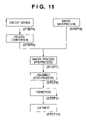
- FIGS. 15A and 15Bare explanatory views (graphs) for explaining line width control of a line pattern.
- FIG. 15Ashows an example of line width control in drawing, e.g., a 48-nm isolated line.
- the formation of, e.g., a line having a width of 48 nmuses three pixels, the doses (exposure times) of which are equalized.
- FIG. 15Bexemplifies a case in which a 45-nm isolated line, for example, is drawn.
- three pixelsare used like the 48-nm isolated line.
- the dose (exposure time) of a pixel positioned at the line edgeis reduced to, e.g., 13/16 that of the other pixels. That is, the dose of a pixel positioned at the line edge is made variable to control a line width (line width imparting amount) that the pixel imparts to the line pattern, thereby forming a pattern having a target line width.
- the dose (exposure time) of a pixel positioned at the line edgeneed not always be 13/16 that of the other pixels.
- an exposure apparatuswhich draws a pattern on a substrate with a charged particle beam.
- the exposure apparatuscomprises a detector configured to detect a charged particle beam, a deflector configured to deflect the charged particle beam to scan the substrate or the detector with the charged particle beam, and a controller configured to control the deflector to scan each of a plurality of scanning ranges on the detector with the charged particle beam, and calculates, based on the charged particle beam amounts detected by the detector upon scanning the plurality of scanning ranges, the intensity distribution of the charged particle beam which strikes the detector.
- a method of measuring the line width of a pattern formed by an exposure apparatus which draws the pattern on a substrate with a charged particle beamincludes a detector which detects a charged particle beam, and a deflector which deflects the charged particle beam to scan the substrate or the detector with the charged particle beam.
- the measurement methodcomprises steps of controlling the deflector to scan each of a plurality of scanning ranges on the detector with the charged particle beam, and calculating, based on the charged particle beam amounts detected by the detector upon scanning the plurality of scanning ranges, the intensity distribution of the charged particle beam which strikes the detector, and calculating, based on the intensity distribution, the line width of a pattern to be formed on the substrate with the charged particle beam.
- FIG. 1is an explanatory view for explaining the outline of the main part of an electron beam exposure apparatus according to an embodiment of the present invention
- FIG. 2is a block diagram showing the system configuration of the exposure apparatus according to the embodiment of the present invention.
- FIG. 3is an explanatory view for explaining a drawing method (charged particle beam drawing method) according to the embodiment of the present invention
- FIG. 4is a table illustrating dose patterns according to the embodiment of the present invention.
- FIGS. 5A and 5Bare explanatory charts for explaining dose patterns and a deflection position coordinate to measure the actual line width of each dose pattern according to the embodiment of the present invention
- FIG. 6is a graph illustrating the intensity distributions of electron beams which strike a semiconductor detector according to the embodiment of the present invention.
- FIG. 7is an explanatory graph showing the relationship between an actual line width and a command line width (dose pattern) according to the embodiment of the present invention.
- FIG. 8is a graph illustrating a correction function of the pulse width (dose command value) according to the embodiment of the present invention.
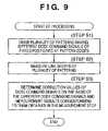
- FIG. 9is a flowchart illustrating a method of determining a correction function of the pulse width (dose command value) according to the embodiment of the present invention.
- FIG. 10is an explanatory graph for explaining the dose pattern correction result according to the embodiment of the present invention.
- FIG. 11is a flowchart for explaining the device manufacture using the exposure apparatus according to the embodiment of the present invention.
- FIG. 12is a flowchart illustrating details of the wafer process (step 7 ) in the flowchart shown in FIG. 11 ;
- FIG. 13is an explanatory view for explaining a conventional raster scanning type electron beam exposure apparatus
- FIG. 14is an explanatory view for explaining the pixel intensity distribution obtained by conventional raster scanning
- FIGS. 15A and 15Bare explanatory graphs for explaining conventional line width control
- FIG. 16is an explanatory table for explaining a conventional dose pattern
- FIG. 17is a flowchart for explaining a line width measurement sequence according to the preferred embodiment of the present invention.
- FIG. 18is a graph when the abscissa as the measurement result illustrated in FIG. 7 is replaced by the sum total of the widths of a plurality of pulses which form a dose pattern;
- FIG. 19is a graph when the abscissa of FIG. 18 is replaced by the width of the fourth pulse and the ordinate of FIG. 18 is replaced by the line width of a pattern formed by the fourth pulse;
- FIG. 20is a flowchart illustrating an example of a correction function determination method according to the preferred embodiment of the present invention.
- a charged particle beamhere includes an ion beam in addition to an electron beam.
- the present inventionis not limited to an exposure apparatus using an electron beam, and is applicable to an exposure apparatus using an ion beam.
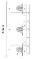
- FIG. 1is a schematic view showing the outline of the main part of an electron beam exposure apparatus according to an embodiment of the present invention.
- an electron beam emitted by an electron gunforms a crossover image.
- This crossover imagewill be referred to as an electron source 1 hereinafter.
- the electron beam emitted by the electron source 1forms an image (SI) 3 of the electron source 1 via a beam shaping optical system 2 .
- a collimator lens 4collimates the electron beam from the image SI 3 into an almost parallel electron beam.
- the almost parallel electron beamilluminates an aperture array 5 having a plurality of apertures.
- the aperture array 5has a plurality of apertures to divide the electron beam into a plurality of electron beams.
- Each of the plurality of electron beams divided by the aperture array 5forms an intermediate image of the image SI 3 via an electro-static lens array 6 having a plurality of electro-static lenses.
- a blanker array 7 having a plurality of blankers serving as electro-static deflectorsis arranged on the side on which the intermediate images are formed.
- a reduction electro-optic system 8 including two-stage symmetrical magnetic doublet lenses 81 and 82is arranged downstream of the side on which the intermediate images are formed.
- the reduction electro-optic system 8projects intermediate images onto a wafer (substrate) 9 .
- the electron beam deflected by the blanker array 7does not strike the wafer 9 because a blanking aperture BA shields it.
- the electron beam which is not deflected by the blanker array 7strikes the wafer 9 because the blanking aperture BA does not shield it.
- the lower-stage doublet lens 82incorporates a deflector 10 for simultaneously displacing a plurality of electron beams to target positions in the X and Y directions, and a focus coil 12 for simultaneously adjusting the focus of a plurality of electron beams.
- An X-Y stage 13supports the wafer 9 and can move in the X and Y directions perpendicular to the optical axis.
- An electro-static chuck 15 and semiconductor detector (SSD) 14are arranged on the X-Y stage 13 .
- the electro-static chuck 15chucks the wafer 9 .
- the semiconductor detector SSD 14has a knife edge on the incident side of an electron beam and measures the electron beam.
- FIG. 2is a block diagram showing the system configuration of the exposure apparatus according to the preferred embodiment of the present invention.
- a blanker array control circuit 21individually controls the plurality of blankers which form the blanker array 7 . With this operation, the blanker array control circuit 21 individually controls whether to allow an electron beam to strike the wafer or semiconductor detector (detector) 14 .
- a deflector control circuit 22controls the deflector 10 .
- An electron beam shape detection circuit 23processes the signal from the semiconductor detector 14 .
- a focus control circuit 24controls the focus position of the reduction electro-optic system 8 by adjusting the focal length of the focus coil 12 .
- a stage driving control circuit 25controls driving of the X-Y stage 13 in cooperation with laser interferometers (not shown) which detect the position of the X-Y stage 13 .
- a main control system (controller) 26is, e.g., a CPU or MPU which controls the plurality of control circuits and manages the overall electron beam exposure apparatus.
- FIG. 3is an explanatory view for explaining a drawing method (charged particle beam drawing method) according to the preferred embodiment of the present invention.
- the main control system 26instructs the deflector control circuit 22 to deflect a plurality of electron beams.
- the main control system 26also instructs the blanker array control circuit 21 to individually turn on/off the blankers of the blanker array 7 based on a command value corresponding to a pixel to be drawn on the wafer 9 .
- the main control system 26instructs, based on exposure control data, the deflector control circuit 22 so that the deflector 10 raster-scans and exposes a corresponding element field EF on the wafer 9 , as shown in FIG. 3 .
- the element fields EF of the respective electron beamsare set to be two-dimensionally adjacent to each other.
- subfields (SF 1 , SF 2 , SF 3 , . . . ) formed by the arrays of a plurality of element fields EFare simultaneously exposed.
- the main control system 26instructs the deflector control circuit 22 so that the deflector 10 deflects the plurality of electron beams, i.e., exposes the next subfield SF 2 , including moving the pattern drawing position in the direction in which the line width is measured.
- the aberration when each electron beam is reduced and projected via the reduction electro-optic system 8also changes.
- FIG. 5Ais a chart showing the deflection position (the position at which an electron beam strikes the wafer or semiconductor detector) of an electron beam. As described above, the deflector 10 controls the position (i.e., the deflection of an electron beam) at which an electron beam strikes the wafer or semiconductor detector 14 .
- FIG. 5Bis a chart showing an example of dose patterns. FIGS. 5A and 5B share a common time axis and illustrate the relationship between the deflection position and the dose pattern.
- the blanker array 7controls irradiation of the electron beam with respect to the semiconductor detector 14 in accordance with the dose pattern as illustrated in FIG. 5B while controlling the deflection of the electron beam.
- an electron beam intensity distribution formed by the electron beam which strikes a detection surface of the semiconductor detector 14is detected.
- This electron beam intensity distributionhas a strong correlation with the width of a latent image pattern formed on the resist by drawing the device pattern on the resist on the wafer with an electron beam, and further with the width of a resist pattern formed by developing the latent image pattern. That is, the width of a portion having a value equal to or higher than the slice level in an electron beam intensity distribution formed on the detection surface of the semiconductor detector in accordance with the dose pattern is equivalent to the width of a latent image pattern formed on the resist in accordance with the dose pattern, and further the width of a resist pattern obtained by developing the latent image pattern.
- FIG. 6is an explanatory graph for explaining the dose pattern of an electron beam which strikes the semiconductor detector (SSD) 14 .
- Rectangles 60indicate individual pulses which form a dose pattern.
- Convex curves 62indicate an electron beam intensity distribution formed on the detection surface of the semiconductor detector 14 in accordance with the dose pattern. This electron beam intensity distribution can be measured in the following way.
- the deflector 10moves, from the scanning start position in the scanning direction, the position at which the electron beam strikes the detection surface of the semiconductor detector 14 . During this time, the semiconductor detector 14 detects the amount of electron beam which strikes it.
- the deflector 10moves, from the changed scanning start position in the scanning direction, the position at which the electron beam strikes the detection surface of the semiconductor detector 14 . During this time, the semiconductor detector 14 detects the amount of electron beam which strikes it. The above-described process is repeated.
- the amount of electron beam detected by the semiconductor detector 14 in every scanningis the amount (a value obtained by integrating the intensity of the electron beam over time) of electron beam which has struck it without being shielded by the knife edge KE arranged on it.
- An electron beamscans the semiconductor detector 14 in accordance with the same dose pattern plural times while changing the scanning start position. Calculating the change amount of the output (electron beam amount) from the semiconductor detector 14 obtained by scanning makes it possible to attain an electron beam intensity distribution.
- Executing the above operation for a plurality of dose patternsmakes it possible to attain the relationship between a dose pattern and the line width of a resist pattern formed in accordance with it. That is, according to this embodiment, it is possible to attain the relationship between a dose pattern and the line width of a resist pattern formed in accordance with it, without developing the resist.
- FIG. 7is a graph illustrating the relationship between a dose pattern and the line width of a resist pattern formed in accordance with it.
- the abscissa of FIG. 7indicates a command line width (target line width) in line width measurement.
- the ordinate of FIG. 7indicates the width of an actually formed line.
- the command line widthis designated in a command sent from the main control system 26 to the blanker array control circuit 21 .
- the command line widthcorresponds to the dose pattern as illustrated in FIG. 4 .
- FIG. 4illustrates sixteen types of dose patterns each of which is formed by four pulses (“first shot”, “second shot”, “third shot”, and “fourth shot”).
- a time period of 1 nscorresponds to a line width of 2 nm.
- the electron beamstrikes the wafer or semiconductor detector 14 for a total of 24 ns and the command line width is 48 nm.
- FIG. 17is a flowchart for explaining a line width measurement sequence according to the preferred embodiment of the present invention.
- Line width measurementis performed under the control of the main control system 26 .
- the main control system 26sends a command to the deflector control circuit 22 to control the deflector 10 to scan the semiconductor detector 14 with an electron beam (charged particle beam).
- This scanningcan be done in accordance with a deflection control profile shown in, e.g., FIG. 5A .
- This profileis used to gradually change the scanning range (deflection range). For example, this profile is used to change the scanning start position in the scanning direction little by little every time the electron beam scans the semiconductor detector 14 .
- a series of plural times of scanning processesuse the same dose pattern.
- the electron beamscans the semiconductor detector 14 as described above, it detects the amount of electron beam (charged particle beam) which strikes it under the control of the main control system 26 .
- # 1 , #i, and #nrespectively indicate the first, i-th, and n-th scanning processes with respect to the semiconductor detector 14 with the electron beam.
- step S 171the semiconductor detector 14 detects the amount of electron beam (charged particle beam) which strikes it while the semiconductor detector 14 is scanned with the electron beam (charged particle beam) for each of a plurality of scanning ranges on the semiconductor detector 14 .
- step S 173the main control system 26 calculates the change amount of the output, i.e., electron beam (charged particle beam) from the semiconductor detector 14 obtained by the plural times of scanning processes in step S 171 , to obtain an electron beam (charged particle beam) intensity distribution.
- the change amount of the outputi.e., electron beam (charged particle beam) from the semiconductor detector 14 obtained by the plural times of scanning processes in step S 171 , to obtain an electron beam (charged particle beam) intensity distribution.
- step S 175the width of a portion having a value equal to or higher than the slice level in the electron beam (charged particle beam) intensity distribution obtained in step S 173 is calculated. That is, the line width of a resist pattern to be formed by drawing a pattern on the resist in accordance with the dose pattern used in step S 171 is calculated.
- the slice levelcan be determined depending on the resist and development condition.
- Each of the plurality of dose patterns as illustrated in FIG. 4undergoes the process shown in FIG. 17 . This makes it possible to obtain the relationship between the dose pattern as illustrated in FIG. 7 and the line width of a resist pattern formed in accordance with it.
- an actual line widthmonotonically increases as the command line width (in this example, the sum total of the pulse widths of a dose pattern) increases.
- FIG. 8is a graph illustrating a correction function f generated on the basis of the measurement result (the relationship between a dose pattern and the line width of a resist pattern formed in accordance with it) illustrated in FIG. 7 .
- An abscissa D 0indicates the pulse width in case where the width of a pulse forming a dose pattern is assumed to have a linear relationship with the line width of an actually formed resist pattern. This pulse width will be called a pre-correction pulse width hereinafter.
- An ordinate D 1indicates the pulse width after the pre-correction pulse width D 0 is corrected in accordance with the correction function f. This pulse width will be called a post-correction pulse width hereinafter. As illustrated in FIG.
- the width (dose command value) of a pulse forming a dose patterndoes not have a linear relationship with the line width of an actually formed resist pattern.
- FIG. 18is a graph when the abscissa as the measurement result illustrated in FIG. 7 is replaced by the sum total of the widths of a plurality of pulses forming a dose pattern.
- a time period of 1 nscorresponds to a line width of 2 nm.
- FIG. 19is a graph when the abscissa of FIG. 18 is replaced by the width of the fourth pulse and the ordinate of FIG. 18 is replaced by the line width of a pattern formed by the fourth pulse.
- a curve 180indicates an actual line width.
- four pulsesform a dose pattern, and its line width is finely adjusted by changing the width of the fourth pulse. It is possible to obtain the correction function f shown in FIG. 8 by adding the difference between the curve 180 and a straight line 181 to the value of a straight line 81 .
- FIG. 20is a flowchart illustrating an example of a correction function determination method according to the preferred embodiment of the present invention. This method is performed under the control of the main control system 26 .
- the main control system 26uses the semiconductor detector 14 to measure, in accordance with the method explained with reference to FIG. 17 , the relationship between a dose pattern and the line width of a resist pattern formed in accordance with it.
- step S 193the main control system 26 determines a correction function f in accordance with the above-described method, based on the result measured in step S 191 . After determining the correction function f, the electron beam exposure apparatus completes calibration.
- a post-correction pulse width D 1may be determined in accordance with the correction function f shown in FIG. 8 by setting, as a pre-correction pulse width D 0 , the width of the fourth pulse of the dose pattern illustrated in FIG. 4 . This makes it possible to correct the pulse width D 0 , thereby obtaining a pattern having the target line width.
- FIG. 9is a flowchart representing the correction function determination method from another viewpoint.
- an electron beamcharged particle beam
- step S 2the pattern line width is measured based on the measurement result of the amount of charged particle beam of each of the plurality of dose patterns.
- a pulse width correction functionis determined based on the different pulse widths (dose command values) and the measurement results corresponding to them.
- the electron beam exposure apparatuscompletes calibration.
- a post-correction pulse width D 1may be determined in accordance with the correction function f shown in FIG. 8 by setting, as a pre-correction pulse width D 0 , the width of the fourth pulse of the dose pattern illustrated in FIG. 4 . This makes it possible to correct the pulse width D 0 , thereby obtaining a pattern having the target line width.
- FIG. 10shows a practical example of a result of correcting the dose pattern shown in FIG. 4 , using the above-described correction function.
- the ordinate of FIG. 10indicates a change in line width, and the abscissa of FIG. 10 indicates the pattern movement amount.
- a change in dose patternis preferably small even when, e.g., the pattern movement amount increases.
- the command valueis corrected in the above way to obtain a corresponding dose. Obviously, this decreases a change in line width due to the pattern movement to improve the reliability of pattern formation.
- the line width of the charged particle beamis efficiently measured and corrected. This makes it possible to easily draw a required micropattern and improve the efficiency and reliability in drawing a required pattern.
- the exposure apparatus(electron beam exposure apparatus) according to this embodiment adopts the charged particle beam drawing method. This allows a required exposure process, an improvement in the yield upon exposing a micropattern, and an improvement in the efficiency and reliability of the exposure process.
- FIG. 11shows a sequence for manufacturing a microdevice (e.g., a semiconductor chip such as an IC or an LSI, a liquid crystal panel, a CCD, a thin-film magnetic head, or a micromachine).
- a microdevicee.g., a semiconductor chip such as an IC or an LSI, a liquid crystal panel, a CCD, a thin-film magnetic head, or a micromachine.
- step 4circuit design
- step 5EB data conversion
- exposure control data of the exposure apparatusis generated on the basis of the designed circuit pattern.
- step 6wafer manufacture
- a waferis manufactured using a material such as silicon.
- step 7wafer process
- a preprocessan actual circuit is formed on the wafer by lithography using the wafer and the exposure apparatus which has received the prepared exposure control data.
- step 8a semiconductor chip is formed from the wafer manufactured in step 7 .
- This stepincludes processes such as assembly (dicing and bonding) and packaging (chip encapsulation).
- step 9inspections including operation check test and durability test of the semiconductor device manufactured in step 8 are performed.
- a semiconductor deviceis completed with these processes and shipped in step 10 .
- FIG. 12shows the detailed sequence of the wafer process (step 7 ).
- step 11oxidation
- step 12CVD
- an insulating filmis formed on the wafer surface.
- step 13electrode formation
- step 14ion implantation
- step 15resist process
- a photosensitive agentis applied to the wafer.
- step 16exposure
- step 17development
- step 18etching
- step 19resist removal
- any unnecessary resist remaining after etchingis removed.
- the device manufacturing method according to this embodimentadopts the above-described electron beam exposure apparatus. This makes it possible to improve the manufacturing yield and increase the efficiency and reliability of microfabrication.
Landscapes
- Engineering & Computer Science (AREA)
- Chemical & Material Sciences (AREA)
- Nanotechnology (AREA)
- Analytical Chemistry (AREA)
- Physics & Mathematics (AREA)
- Crystallography & Structural Chemistry (AREA)
- Theoretical Computer Science (AREA)
- Mathematical Physics (AREA)
- Condensed Matter Physics & Semiconductors (AREA)
- General Physics & Mathematics (AREA)
- Manufacturing & Machinery (AREA)
- Exposure And Positioning Against Photoresist Photosensitive Materials (AREA)
- Electron Beam Exposure (AREA)
Abstract
Description
D1=f(D0) (1)
- D0: pre-correction pulse width (pre-correction dose command value)
- D1: post-correction pulse width (post-correction dose command value)
Claims (8)
Applications Claiming Priority (3)
| Application Number | Priority Date | Filing Date | Title |
|---|---|---|---|
| JP2006-169798(PAT.) | 2006-06-20 | ||
| JP2006169798AJP5116996B2 (en) | 2006-06-20 | 2006-06-20 | Charged particle beam drawing method, exposure apparatus, and device manufacturing method |
| JP2006-169798 | 2006-06-20 |
Publications (2)
| Publication Number | Publication Date |
|---|---|
| US20080067403A1 US20080067403A1 (en) | 2008-03-20 |
| US7692166B2true US7692166B2 (en) | 2010-04-06 |
Family
ID=39008772
Family Applications (1)
| Application Number | Title | Priority Date | Filing Date |
|---|---|---|---|
| US11/762,182Expired - Fee RelatedUS7692166B2 (en) | 2006-06-20 | 2007-06-13 | Charged particle beam exposure apparatus |
Country Status (2)
| Country | Link |
|---|---|
| US (1) | US7692166B2 (en) |
| JP (1) | JP5116996B2 (en) |
Cited By (28)
| Publication number | Priority date | Publication date | Assignee | Title |
|---|---|---|---|---|
| US8791656B1 (en) | 2013-05-31 | 2014-07-29 | Mevion Medical Systems, Inc. | Active return system |
| US8907311B2 (en) | 2005-11-18 | 2014-12-09 | Mevion Medical Systems, Inc. | Charged particle radiation therapy |
| US8927950B2 (en) | 2012-09-28 | 2015-01-06 | Mevion Medical Systems, Inc. | Focusing a particle beam |
| US8933650B2 (en) | 2007-11-30 | 2015-01-13 | Mevion Medical Systems, Inc. | Matching a resonant frequency of a resonant cavity to a frequency of an input voltage |
| US8941083B2 (en) | 2007-10-11 | 2015-01-27 | Mevion Medical Systems, Inc. | Applying a particle beam to a patient |
| US8952634B2 (en) | 2004-07-21 | 2015-02-10 | Mevion Medical Systems, Inc. | Programmable radio frequency waveform generator for a synchrocyclotron |
| US8970137B2 (en) | 2007-11-30 | 2015-03-03 | Mevion Medical Systems, Inc. | Interrupted particle source |
| US9155186B2 (en) | 2012-09-28 | 2015-10-06 | Mevion Medical Systems, Inc. | Focusing a particle beam using magnetic field flutter |
| US9185789B2 (en) | 2012-09-28 | 2015-11-10 | Mevion Medical Systems, Inc. | Magnetic shims to alter magnetic fields |
| US9301384B2 (en) | 2012-09-28 | 2016-03-29 | Mevion Medical Systems, Inc. | Adjusting energy of a particle beam |
| US9545528B2 (en) | 2012-09-28 | 2017-01-17 | Mevion Medical Systems, Inc. | Controlling particle therapy |
| US9622335B2 (en) | 2012-09-28 | 2017-04-11 | Mevion Medical Systems, Inc. | Magnetic field regenerator |
| US9661736B2 (en) | 2014-02-20 | 2017-05-23 | Mevion Medical Systems, Inc. | Scanning system for a particle therapy system |
| US9681531B2 (en) | 2012-09-28 | 2017-06-13 | Mevion Medical Systems, Inc. | Control system for a particle accelerator |
| US9723705B2 (en) | 2012-09-28 | 2017-08-01 | Mevion Medical Systems, Inc. | Controlling intensity of a particle beam |
| US9730308B2 (en) | 2013-06-12 | 2017-08-08 | Mevion Medical Systems, Inc. | Particle accelerator that produces charged particles having variable energies |
| US9950194B2 (en) | 2014-09-09 | 2018-04-24 | Mevion Medical Systems, Inc. | Patient positioning system |
| US9962560B2 (en) | 2013-12-20 | 2018-05-08 | Mevion Medical Systems, Inc. | Collimator and energy degrader |
| US10254739B2 (en) | 2012-09-28 | 2019-04-09 | Mevion Medical Systems, Inc. | Coil positioning system |
| US10258810B2 (en) | 2013-09-27 | 2019-04-16 | Mevion Medical Systems, Inc. | Particle beam scanning |
| US10646728B2 (en) | 2015-11-10 | 2020-05-12 | Mevion Medical Systems, Inc. | Adaptive aperture |
| US10653892B2 (en) | 2017-06-30 | 2020-05-19 | Mevion Medical Systems, Inc. | Configurable collimator controlled using linear motors |
| US10675487B2 (en) | 2013-12-20 | 2020-06-09 | Mevion Medical Systems, Inc. | Energy degrader enabling high-speed energy switching |
| US10925147B2 (en) | 2016-07-08 | 2021-02-16 | Mevion Medical Systems, Inc. | Treatment planning |
| US11103730B2 (en) | 2017-02-23 | 2021-08-31 | Mevion Medical Systems, Inc. | Automated treatment in particle therapy |
| US11117195B2 (en) | 2018-07-19 | 2021-09-14 | The University Of Liverpool | System and process for in-process electron beam profile and location analyses |
| US11532760B2 (en) | 2017-05-22 | 2022-12-20 | Howmedica Osteonics Corp. | Device for in-situ fabrication process monitoring and feedback control of an electron beam additive manufacturing process |
| US11717703B2 (en) | 2019-03-08 | 2023-08-08 | Mevion Medical Systems, Inc. | Delivery of radiation by column and generating a treatment plan therefor |
Families Citing this family (5)
| Publication number | Priority date | Publication date | Assignee | Title |
|---|---|---|---|---|
| EP2450079B1 (en) | 2009-07-01 | 2015-02-25 | Toppan Printing Co., Ltd. | Needle-like material |
| US20120112091A1 (en)* | 2010-11-04 | 2012-05-10 | National Taiwan University | Method for adjusting status of particle beams for patterning a substrate and system using the same |
| JP6277953B2 (en) | 2012-02-29 | 2018-02-14 | 凸版印刷株式会社 | Manufacturing method of needle-shaped body |
| CN105301472A (en)* | 2015-11-04 | 2016-02-03 | 天津津航计算技术研究所 | Space single-particle turning rate measurement system |
| US11036147B2 (en)* | 2019-03-20 | 2021-06-15 | Kla Corporation | System and method for converting backside surface roughness to frontside overlay |
Citations (10)
| Publication number | Priority date | Publication date | Assignee | Title |
|---|---|---|---|---|
| US5396077A (en)* | 1993-03-18 | 1995-03-07 | Hitachi, Ltd. | Electron beam lithography apparatus having electron optics correction system |
| US5432352A (en) | 1993-09-20 | 1995-07-11 | Eaton Corporation | Ion beam scan control |
| US5863682A (en) | 1996-02-23 | 1999-01-26 | Kabushiki Kaisha Toshiba | Charged particle beam writing method for determining optimal exposure dose prior to pattern drawing |
| US5981961A (en) | 1996-03-15 | 1999-11-09 | Applied Materials, Inc. | Apparatus and method for improved scanning efficiency in an ion implanter |
| US6835937B1 (en) | 1999-12-13 | 2004-12-28 | Canon Kabushiki Kaisha | Correcting method for correcting exposure data used for a charged particle beam exposure system |
| JP2005032838A (en) | 2003-07-08 | 2005-02-03 | Canon Inc | Charged particle beam drawing method and apparatus, and device manufacturing method |
| US6870170B1 (en) | 2004-03-04 | 2005-03-22 | Applied Materials, Inc. | Ion implant dose control |
| US7282427B1 (en) | 2006-05-04 | 2007-10-16 | Applied Materials, Inc. | Method of implanting a substrate and an ion implanter for performing the method |
| US20080067402A1 (en)* | 2006-06-20 | 2008-03-20 | Masato Muraki | Charged particle beam exposure apparatus |
| US7462848B2 (en)* | 2003-10-07 | 2008-12-09 | Multibeam Systems, Inc. | Optics for generation of high current density patterned charged particle beams |
Family Cites Families (5)
| Publication number | Priority date | Publication date | Assignee | Title |
|---|---|---|---|---|
| JPH0391228A (en)* | 1989-09-01 | 1991-04-16 | Jeol Ltd | Measuring method of diameter of charged particle beam |
| JPH04116915A (en)* | 1990-09-07 | 1992-04-17 | Jeol Ltd | Drawing beam diameter adjustment method |
| JP2000349016A (en)* | 1999-06-07 | 2000-12-15 | Sony Corp | Plotting method, mask for exposure and manufacture of mask for exposure as well as semiconductor device and its manufacture |
| JP2005026527A (en)* | 2003-07-03 | 2005-01-27 | Sony Corp | Method of exposure and method of manufacturing semiconductor device |
| JP4402529B2 (en)* | 2004-06-30 | 2010-01-20 | キヤノン株式会社 | Charged particle beam exposure method, charged particle beam exposure apparatus and device manufacturing method |
- 2006
- 2006-06-20JPJP2006169798Apatent/JP5116996B2/ennot_activeExpired - Fee Related
- 2007
- 2007-06-13USUS11/762,182patent/US7692166B2/ennot_activeExpired - Fee Related
Patent Citations (10)
| Publication number | Priority date | Publication date | Assignee | Title |
|---|---|---|---|---|
| US5396077A (en)* | 1993-03-18 | 1995-03-07 | Hitachi, Ltd. | Electron beam lithography apparatus having electron optics correction system |
| US5432352A (en) | 1993-09-20 | 1995-07-11 | Eaton Corporation | Ion beam scan control |
| US5863682A (en) | 1996-02-23 | 1999-01-26 | Kabushiki Kaisha Toshiba | Charged particle beam writing method for determining optimal exposure dose prior to pattern drawing |
| US5981961A (en) | 1996-03-15 | 1999-11-09 | Applied Materials, Inc. | Apparatus and method for improved scanning efficiency in an ion implanter |
| US6835937B1 (en) | 1999-12-13 | 2004-12-28 | Canon Kabushiki Kaisha | Correcting method for correcting exposure data used for a charged particle beam exposure system |
| JP2005032838A (en) | 2003-07-08 | 2005-02-03 | Canon Inc | Charged particle beam drawing method and apparatus, and device manufacturing method |
| US7462848B2 (en)* | 2003-10-07 | 2008-12-09 | Multibeam Systems, Inc. | Optics for generation of high current density patterned charged particle beams |
| US6870170B1 (en) | 2004-03-04 | 2005-03-22 | Applied Materials, Inc. | Ion implant dose control |
| US7282427B1 (en) | 2006-05-04 | 2007-10-16 | Applied Materials, Inc. | Method of implanting a substrate and an ion implanter for performing the method |
| US20080067402A1 (en)* | 2006-06-20 | 2008-03-20 | Masato Muraki | Charged particle beam exposure apparatus |
Non-Patent Citations (1)
| Title |
|---|
| The above references were cited in a Sep. 11, 2009 U.S. Office Action that issued in related U.S. Appl. No. 11/762,180. |
Cited By (47)
| Publication number | Priority date | Publication date | Assignee | Title |
|---|---|---|---|---|
| US8952634B2 (en) | 2004-07-21 | 2015-02-10 | Mevion Medical Systems, Inc. | Programmable radio frequency waveform generator for a synchrocyclotron |
| USRE48047E1 (en) | 2004-07-21 | 2020-06-09 | Mevion Medical Systems, Inc. | Programmable radio frequency waveform generator for a synchrocyclotron |
| US10722735B2 (en) | 2005-11-18 | 2020-07-28 | Mevion Medical Systems, Inc. | Inner gantry |
| US8907311B2 (en) | 2005-11-18 | 2014-12-09 | Mevion Medical Systems, Inc. | Charged particle radiation therapy |
| US8916843B2 (en) | 2005-11-18 | 2014-12-23 | Mevion Medical Systems, Inc. | Inner gantry |
| US9925395B2 (en) | 2005-11-18 | 2018-03-27 | Mevion Medical Systems, Inc. | Inner gantry |
| US10279199B2 (en) | 2005-11-18 | 2019-05-07 | Mevion Medical Systems, Inc. | Inner gantry |
| US9452301B2 (en) | 2005-11-18 | 2016-09-27 | Mevion Medical Systems, Inc. | Inner gantry |
| US8941083B2 (en) | 2007-10-11 | 2015-01-27 | Mevion Medical Systems, Inc. | Applying a particle beam to a patient |
| US8933650B2 (en) | 2007-11-30 | 2015-01-13 | Mevion Medical Systems, Inc. | Matching a resonant frequency of a resonant cavity to a frequency of an input voltage |
| US8970137B2 (en) | 2007-11-30 | 2015-03-03 | Mevion Medical Systems, Inc. | Interrupted particle source |
| USRE48317E1 (en) | 2007-11-30 | 2020-11-17 | Mevion Medical Systems, Inc. | Interrupted particle source |
| US10368429B2 (en) | 2012-09-28 | 2019-07-30 | Mevion Medical Systems, Inc. | Magnetic field regenerator |
| US9723705B2 (en) | 2012-09-28 | 2017-08-01 | Mevion Medical Systems, Inc. | Controlling intensity of a particle beam |
| US9681531B2 (en) | 2012-09-28 | 2017-06-13 | Mevion Medical Systems, Inc. | Control system for a particle accelerator |
| US9545528B2 (en) | 2012-09-28 | 2017-01-17 | Mevion Medical Systems, Inc. | Controlling particle therapy |
| US9706636B2 (en) | 2012-09-28 | 2017-07-11 | Mevion Medical Systems, Inc. | Adjusting energy of a particle beam |
| US9301384B2 (en) | 2012-09-28 | 2016-03-29 | Mevion Medical Systems, Inc. | Adjusting energy of a particle beam |
| US9622335B2 (en) | 2012-09-28 | 2017-04-11 | Mevion Medical Systems, Inc. | Magnetic field regenerator |
| US9185789B2 (en) | 2012-09-28 | 2015-11-10 | Mevion Medical Systems, Inc. | Magnetic shims to alter magnetic fields |
| US9155186B2 (en) | 2012-09-28 | 2015-10-06 | Mevion Medical Systems, Inc. | Focusing a particle beam using magnetic field flutter |
| US8927950B2 (en) | 2012-09-28 | 2015-01-06 | Mevion Medical Systems, Inc. | Focusing a particle beam |
| US10155124B2 (en) | 2012-09-28 | 2018-12-18 | Mevion Medical Systems, Inc. | Controlling particle therapy |
| US10254739B2 (en) | 2012-09-28 | 2019-04-09 | Mevion Medical Systems, Inc. | Coil positioning system |
| US8791656B1 (en) | 2013-05-31 | 2014-07-29 | Mevion Medical Systems, Inc. | Active return system |
| US9730308B2 (en) | 2013-06-12 | 2017-08-08 | Mevion Medical Systems, Inc. | Particle accelerator that produces charged particles having variable energies |
| US10258810B2 (en) | 2013-09-27 | 2019-04-16 | Mevion Medical Systems, Inc. | Particle beam scanning |
| US10456591B2 (en) | 2013-09-27 | 2019-10-29 | Mevion Medical Systems, Inc. | Particle beam scanning |
| US9962560B2 (en) | 2013-12-20 | 2018-05-08 | Mevion Medical Systems, Inc. | Collimator and energy degrader |
| US10675487B2 (en) | 2013-12-20 | 2020-06-09 | Mevion Medical Systems, Inc. | Energy degrader enabling high-speed energy switching |
| US9661736B2 (en) | 2014-02-20 | 2017-05-23 | Mevion Medical Systems, Inc. | Scanning system for a particle therapy system |
| US11717700B2 (en) | 2014-02-20 | 2023-08-08 | Mevion Medical Systems, Inc. | Scanning system |
| US10434331B2 (en) | 2014-02-20 | 2019-10-08 | Mevion Medical Systems, Inc. | Scanning system |
| US9950194B2 (en) | 2014-09-09 | 2018-04-24 | Mevion Medical Systems, Inc. | Patient positioning system |
| US11213697B2 (en) | 2015-11-10 | 2022-01-04 | Mevion Medical Systems, Inc. | Adaptive aperture |
| US10786689B2 (en) | 2015-11-10 | 2020-09-29 | Mevion Medical Systems, Inc. | Adaptive aperture |
| US10646728B2 (en) | 2015-11-10 | 2020-05-12 | Mevion Medical Systems, Inc. | Adaptive aperture |
| US11786754B2 (en) | 2015-11-10 | 2023-10-17 | Mevion Medical Systems, Inc. | Adaptive aperture |
| US10925147B2 (en) | 2016-07-08 | 2021-02-16 | Mevion Medical Systems, Inc. | Treatment planning |
| US12150235B2 (en) | 2016-07-08 | 2024-11-19 | Mevion Medical Systems, Inc. | Treatment planning |
| US11103730B2 (en) | 2017-02-23 | 2021-08-31 | Mevion Medical Systems, Inc. | Automated treatment in particle therapy |
| US11532760B2 (en) | 2017-05-22 | 2022-12-20 | Howmedica Osteonics Corp. | Device for in-situ fabrication process monitoring and feedback control of an electron beam additive manufacturing process |
| US10653892B2 (en) | 2017-06-30 | 2020-05-19 | Mevion Medical Systems, Inc. | Configurable collimator controlled using linear motors |
| US11117195B2 (en) | 2018-07-19 | 2021-09-14 | The University Of Liverpool | System and process for in-process electron beam profile and location analyses |
| US11717703B2 (en) | 2019-03-08 | 2023-08-08 | Mevion Medical Systems, Inc. | Delivery of radiation by column and generating a treatment plan therefor |
| US12161885B2 (en) | 2019-03-08 | 2024-12-10 | Mevion Medical Systems, Inc. | Delivery of radiation by column and generating a treatment plan therefor |
| US12168147B2 (en) | 2019-03-08 | 2024-12-17 | Mevion Medical Systems, Inc. | Collimator and energy degrader for a particle therapy system |
Also Published As
| Publication number | Publication date |
|---|---|
| JP5116996B2 (en) | 2013-01-09 |
| JP2008004597A (en) | 2008-01-10 |
| US20080067403A1 (en) | 2008-03-20 |
Similar Documents
| Publication | Publication Date | Title |
|---|---|---|
| US7692166B2 (en) | Charged particle beam exposure apparatus | |
| EP1505630B1 (en) | Charged particle beam exposure method and apparatus and device manufacturing method using the apparatus | |
| US6835937B1 (en) | Correcting method for correcting exposure data used for a charged particle beam exposure system | |
| US9373424B2 (en) | Electron beam writing apparatus and electron beam writing method | |
| EP1351272A2 (en) | Electron beam exposure method and apparatus and device manufacturing method using the same | |
| JP5835892B2 (en) | Charged particle beam drawing apparatus and device manufacturing method | |
| US6917048B2 (en) | Methods and devices for controlling blur resulting from the space-charge effect and geometrical aberration in a charged-particle-beam microlithography apparatus | |
| US7378671B2 (en) | Aberration measuring apparatus for charged particle beam optical system, charged particle beam lithography machine having the aberration measuring apparatus, and device fabrication method using the apparatus | |
| JP2008041890A (en) | Multi charged particle beam measurement method, exposure apparatus, and device manufacturing method | |
| US7388214B2 (en) | Charged-particle beam exposure apparatus and method | |
| US8692218B2 (en) | Charged particle beam exposure apparatus | |
| US9472372B2 (en) | Charged particle beam writing apparatus and charged particle beam writing method | |
| US11740546B2 (en) | Multi charged particle beam writing apparatus and method of adjusting same | |
| JP4365579B2 (en) | Electron beam exposure apparatus and electron beam exposure method | |
| US7005659B2 (en) | Charged particle beam exposure apparatus, charged particle beam exposure method, and device manufacturing method using the same apparatus | |
| US20150131075A1 (en) | Drawing apparatus, and method of manufacturing article | |
| US20050006603A1 (en) | Charged particle beam exposure method, charged particle beam exposure apparatus, and device manufacturing method | |
| US20150129779A1 (en) | Drawing apparatus, and method of manufacturing article | |
| US20210027986A1 (en) | Multi-beam writing method and multi-beam writing apparatus | |
| US6376137B1 (en) | Charged-particle-beam microlithography apparatus and methods including correction of stage-positioning errors using a deflector | |
| US7394068B2 (en) | Mask inspection apparatus, mask inspection method, and electron beam exposure system | |
| JP4494734B2 (en) | Charged particle beam drawing method, charged particle beam exposure apparatus, and device manufacturing method | |
| JP2006210455A (en) | Charged particle beam exposure apparatus and device manufacturing method using the apparatus | |
| JP4402529B2 (en) | Charged particle beam exposure method, charged particle beam exposure apparatus and device manufacturing method | |
| JP2025080088A (en) | Charged particle beam drawing apparatus, drift amount calculation method, and charged particle beam drawing method |
Legal Events
| Date | Code | Title | Description |
|---|---|---|---|
| AS | Assignment | Owner name:CANON KABUSHIKI KAISHA, JAPAN Free format text:ASSIGNMENT OF ASSIGNORS INTEREST;ASSIGNORS:MURAKI, MASATO;YODA, HARUO;REEL/FRAME:019608/0656;SIGNING DATES FROM 20070704 TO 20070712 Owner name:HITACHI HIGH-TECHNOLOGIES CORPORATION, JAPAN Free format text:ASSIGNMENT OF ASSIGNORS INTEREST;ASSIGNORS:MURAKI, MASATO;YODA, HARUO;REEL/FRAME:019608/0656;SIGNING DATES FROM 20070704 TO 20070712 Owner name:CANON KABUSHIKI KAISHA,JAPAN Free format text:ASSIGNMENT OF ASSIGNORS INTEREST;ASSIGNORS:MURAKI, MASATO;YODA, HARUO;SIGNING DATES FROM 20070704 TO 20070712;REEL/FRAME:019608/0656 Owner name:HITACHI HIGH-TECHNOLOGIES CORPORATION,JAPAN Free format text:ASSIGNMENT OF ASSIGNORS INTEREST;ASSIGNORS:MURAKI, MASATO;YODA, HARUO;SIGNING DATES FROM 20070704 TO 20070712;REEL/FRAME:019608/0656 | |
| FEPP | Fee payment procedure | Free format text:PAYOR NUMBER ASSIGNED (ORIGINAL EVENT CODE: ASPN); ENTITY STATUS OF PATENT OWNER: LARGE ENTITY | |
| STCF | Information on status: patent grant | Free format text:PATENTED CASE | |
| CC | Certificate of correction | ||
| FPAY | Fee payment | Year of fee payment:4 | |
| AS | Assignment | Owner name:CANON KABUSHIKI KAISHA, JAPAN Free format text:ASSIGNMENT OF ASSIGNORS INTEREST;ASSIGNOR:CANON KABUSHIKI KAISHA;REEL/FRAME:040717/0127 Effective date:20160315 Owner name:CANON KABUSHIKI KAISHA, JAPAN Free format text:ASSIGNMENT OF ASSIGNORS INTEREST;ASSIGNORS:HITACHI HIGH-TECHNOLOGIES CORPORATION;CANON KABUSHI KAISHA;REEL/FRAME:040717/0153 Effective date:20160315 | |
| MAFP | Maintenance fee payment | Free format text:PAYMENT OF MAINTENANCE FEE, 8TH YEAR, LARGE ENTITY (ORIGINAL EVENT CODE: M1552) Year of fee payment:8 | |
| AS | Assignment | Owner name:HITACHI HIGH-TECH CORPORATION, JAPAN Free format text:CHANGE OF NAME AND ADDRESS;ASSIGNOR:HITACHI HIGH-TECHNOLOGIES CORPORATION;REEL/FRAME:052259/0227 Effective date:20200212 | |
| FEPP | Fee payment procedure | Free format text:MAINTENANCE FEE REMINDER MAILED (ORIGINAL EVENT CODE: REM.); ENTITY STATUS OF PATENT OWNER: LARGE ENTITY | |
| LAPS | Lapse for failure to pay maintenance fees | Free format text:PATENT EXPIRED FOR FAILURE TO PAY MAINTENANCE FEES (ORIGINAL EVENT CODE: EXP.); ENTITY STATUS OF PATENT OWNER: LARGE ENTITY | |
| STCH | Information on status: patent discontinuation | Free format text:PATENT EXPIRED DUE TO NONPAYMENT OF MAINTENANCE FEES UNDER 37 CFR 1.362 | |
| FP | Lapsed due to failure to pay maintenance fee | Effective date:20220406 |