US7691757B2 - Deposition of complex nitride films - Google Patents
Deposition of complex nitride filmsDownload PDFInfo
- Publication number
- US7691757B2 US7691757B2US11/766,718US76671807AUS7691757B2US 7691757 B2US7691757 B2US 7691757B2US 76671807 AUS76671807 AUS 76671807AUS 7691757 B2US7691757 B2US 7691757B2
- Authority
- US
- United States
- Prior art keywords
- metal halide
- pulses
- flowing
- precursor
- nitrogen
- Prior art date
- Legal status (The legal status is an assumption and is not a legal conclusion. Google has not performed a legal analysis and makes no representation as to the accuracy of the status listed.)
- Active, expires
Links
- 150000004767nitridesChemical class0.000titleclaimsabstractdescription26
- 230000008021depositionEffects0.000titleabstractdescription26
- 239000002243precursorSubstances0.000claimsabstractdescription75
- 229910001507metal halideInorganic materials0.000claimsabstractdescription55
- 150000005309metal halidesChemical class0.000claimsabstractdescription55
- 238000000034methodMethods0.000claimsabstractdescription40
- 238000000151depositionMethods0.000claimsabstractdescription26
- QJGQUHMNIGDVPM-UHFFFAOYSA-Nnitrogen groupChemical group[N]QJGQUHMNIGDVPM-UHFFFAOYSA-N0.000claimsabstractdescription21
- 229910052751metalInorganic materials0.000claimsabstractdescription18
- 239000002184metalSubstances0.000claimsabstractdescription18
- 238000006243chemical reactionMethods0.000claimsdescription38
- 239000000758substrateSubstances0.000claimsdescription13
- 229910052801chlorineInorganic materials0.000claimsdescription9
- 229910008482TiSiNInorganic materials0.000claimsdescription8
- QRXWMOHMRWLFEY-UHFFFAOYSA-NisoniazideChemical compoundNNC(=O)C1=CC=NC=C1QRXWMOHMRWLFEY-UHFFFAOYSA-N0.000claimsdescription8
- 229910052782aluminiumInorganic materials0.000claimsdescription7
- 229910052719titaniumInorganic materials0.000claimsdescription7
- 229910052735hafniumInorganic materials0.000claimsdescription6
- 238000010438heat treatmentMethods0.000claimsdescription6
- 229910052750molybdenumInorganic materials0.000claimsdescription6
- 229910052758niobiumInorganic materials0.000claimsdescription6
- 229910052715tantalumInorganic materials0.000claimsdescription6
- 229910052804chromiumInorganic materials0.000claimsdescription5
- 229910052721tungstenInorganic materials0.000claimsdescription5
- 229910052720vanadiumInorganic materials0.000claimsdescription5
- 229910052726zirconiumInorganic materials0.000claimsdescription5
- 229910004200TaSiNInorganic materials0.000claimsdescription4
- 229910010037TiAlNInorganic materials0.000claimsdescription4
- 229910052732germaniumInorganic materials0.000claimsdescription4
- 229910052710siliconInorganic materials0.000claimsdescription4
- 229910052796boronInorganic materials0.000claimsdescription3
- 229910004491TaAlNInorganic materials0.000claimsdescription2
- 229910052794bromiumInorganic materials0.000claimsdescription2
- 229910052731fluorineInorganic materials0.000claimsdescription2
- 229910052740iodineInorganic materials0.000claimsdescription2
- 229910052736halogenInorganic materials0.000claims1
- 150000002367halogensChemical class0.000claims1
- QGZKDVFQNNGYKY-UHFFFAOYSA-NAmmoniaChemical compoundNQGZKDVFQNNGYKY-UHFFFAOYSA-N0.000abstractdescription49
- 238000005229chemical vapour depositionMethods0.000abstractdescription17
- 229910021529ammoniaInorganic materials0.000abstractdescription4
- 229910000069nitrogen hydrideInorganic materials0.000description41
- 239000010408filmSubstances0.000description25
- 229910003074TiCl4Inorganic materials0.000description19
- 230000008569processEffects0.000description19
- XJDNKRIXUMDJCW-UHFFFAOYSA-Jtitanium tetrachlorideChemical compoundCl[Ti](Cl)(Cl)ClXJDNKRIXUMDJCW-UHFFFAOYSA-J0.000description19
- 239000007789gasSubstances0.000description16
- 239000000463materialSubstances0.000description13
- VSCWAEJMTAWNJL-UHFFFAOYSA-Kaluminium chlorideSubstancesCl[Al](Cl)ClVSCWAEJMTAWNJL-UHFFFAOYSA-K0.000description11
- 150000004820halidesChemical class0.000description11
- 239000000460chlorineSubstances0.000description9
- IJGRMHOSHXDMSA-UHFFFAOYSA-NAtomic nitrogenChemical compoundN#NIJGRMHOSHXDMSA-UHFFFAOYSA-N0.000description7
- 239000010936titaniumSubstances0.000description7
- ZAMOUSCENKQFHK-UHFFFAOYSA-NChlorine atomChemical compound[Cl]ZAMOUSCENKQFHK-UHFFFAOYSA-N0.000description6
- 238000000231atomic layer depositionMethods0.000description6
- 238000010926purgeMethods0.000description5
- 239000004065semiconductorSubstances0.000description5
- 229910003910SiCl4Inorganic materials0.000description4
- ATJFFYVFTNAWJD-UHFFFAOYSA-NTinChemical group[Sn]ATJFFYVFTNAWJD-UHFFFAOYSA-N0.000description4
- 230000008901benefitEffects0.000description4
- 238000005137deposition processMethods0.000description4
- FDNAPBUWERUEDA-UHFFFAOYSA-Nsilicon tetrachlorideChemical compoundCl[Si](Cl)(Cl)ClFDNAPBUWERUEDA-UHFFFAOYSA-N0.000description4
- HSFWRNGVRCDJHI-UHFFFAOYSA-NAcetyleneChemical compoundC#CHSFWRNGVRCDJHI-UHFFFAOYSA-N0.000description3
- UHOVQNZJYSORNB-UHFFFAOYSA-NBenzeneChemical compoundC1=CC=CC=C1UHOVQNZJYSORNB-UHFFFAOYSA-N0.000description3
- OKTJSMMVPCPJKN-UHFFFAOYSA-NCarbonChemical group[C]OKTJSMMVPCPJKN-UHFFFAOYSA-N0.000description3
- OAKJQQAXSVQMHS-UHFFFAOYSA-NHydrazineChemical compoundNNOAKJQQAXSVQMHS-UHFFFAOYSA-N0.000description3
- 239000003795chemical substances by applicationSubstances0.000description3
- 238000013461designMethods0.000description3
- 238000010348incorporationMethods0.000description3
- 150000002739metalsChemical class0.000description3
- 239000000203mixtureSubstances0.000description3
- 229910052757nitrogenInorganic materials0.000description3
- MNWRORMXBIWXCI-UHFFFAOYSA-Ntetrakis(dimethylamido)titaniumChemical compoundCN(C)[Ti](N(C)C)(N(C)C)N(C)CMNWRORMXBIWXCI-UHFFFAOYSA-N0.000description3
- 229910015221MoCl5Inorganic materials0.000description2
- QQONPFPTGQHPMA-UHFFFAOYSA-NPropeneChemical compoundCC=CQQONPFPTGQHPMA-UHFFFAOYSA-N0.000description2
- 229910004537TaCl5Inorganic materials0.000description2
- XAGFODPZIPBFFR-UHFFFAOYSA-NaluminiumChemical compound[Al]XAGFODPZIPBFFR-UHFFFAOYSA-N0.000description2
- 230000009286beneficial effectEffects0.000description2
- 239000011203carbon fibre reinforced carbonSubstances0.000description2
- 239000000470constituentSubstances0.000description2
- 239000003446ligandSubstances0.000description2
- 238000004519manufacturing processMethods0.000description2
- 238000012986modificationMethods0.000description2
- 230000004048modificationEffects0.000description2
- GICWIDZXWJGTCI-UHFFFAOYSA-Imolybdenum pentachlorideChemical compoundCl[Mo](Cl)(Cl)(Cl)ClGICWIDZXWJGTCI-UHFFFAOYSA-I0.000description2
- 229910052756noble gasInorganic materials0.000description2
- 230000003647oxidationEffects0.000description2
- 238000007254oxidation reactionMethods0.000description2
- 239000000376reactantSubstances0.000description2
- 230000009467reductionEffects0.000description2
- 239000002356single layerSubstances0.000description2
- OEIMLTQPLAGXMX-UHFFFAOYSA-Itantalum(v) chlorideChemical compoundCl[Ta](Cl)(Cl)(Cl)ClOEIMLTQPLAGXMX-UHFFFAOYSA-I0.000description2
- 238000005979thermal decomposition reactionMethods0.000description2
- 229910015844BCl3Inorganic materials0.000description1
- ZOXJGFHDIHLPTG-UHFFFAOYSA-NBoronChemical compound[B]ZOXJGFHDIHLPTG-UHFFFAOYSA-N0.000description1
- CPELXLSAUQHCOX-UHFFFAOYSA-MBromideChemical compound[Br-]CPELXLSAUQHCOX-UHFFFAOYSA-M0.000description1
- VEXZGXHMUGYJMC-UHFFFAOYSA-MChloride anionChemical compound[Cl-]VEXZGXHMUGYJMC-UHFFFAOYSA-M0.000description1
- 229910021557Chromium(IV) chlorideInorganic materials0.000description1
- OTMSDBZUPAUEDD-UHFFFAOYSA-NEthaneChemical compoundCCOTMSDBZUPAUEDD-UHFFFAOYSA-N0.000description1
- KRHYYFGTRYWZRS-UHFFFAOYSA-MFluoride anionChemical compound[F-]KRHYYFGTRYWZRS-UHFFFAOYSA-M0.000description1
- 229910006113GeCl4Inorganic materials0.000description1
- 229910003865HfCl4Inorganic materials0.000description1
- 229910015253MoF5Inorganic materials0.000description1
- 229910015255MoF6Inorganic materials0.000description1
- 229910019804NbCl5Inorganic materials0.000description1
- 229910003818SiH2Cl2Inorganic materials0.000description1
- 229910003826SiH3ClInorganic materials0.000description1
- 229910003822SiHCl3Inorganic materials0.000description1
- BLRPTPMANUNPDV-UHFFFAOYSA-NSilaneChemical compound[SiH4]BLRPTPMANUNPDV-UHFFFAOYSA-N0.000description1
- RTAQQCXQSZGOHL-UHFFFAOYSA-NTitaniumChemical compound[Ti]RTAQQCXQSZGOHL-UHFFFAOYSA-N0.000description1
- 229910021553Vanadium(V) chlorideInorganic materials0.000description1
- 229910003091WCl6Inorganic materials0.000description1
- 229910007932ZrCl4Inorganic materials0.000description1
- 150000001336alkenesChemical class0.000description1
- 230000004075alterationEffects0.000description1
- 125000004429atomChemical group0.000description1
- 230000004888barrier functionEffects0.000description1
- 239000001273butaneSubstances0.000description1
- 229910052799carbonInorganic materials0.000description1
- 125000001309chloro groupChemical groupCl*0.000description1
- SLLGVCUQYRMELA-UHFFFAOYSA-NchlorosiliconChemical compoundCl[Si]SLLGVCUQYRMELA-UHFFFAOYSA-N0.000description1
- 238000010276constructionMethods0.000description1
- -1cycloheptheneNatural products0.000description1
- 125000000058cyclopentadienyl groupChemical groupC1(=CC=CC1)*0.000description1
- WADSLQQIOJIXTB-UHFFFAOYSA-LdichloroalumaneChemical compoundCl[AlH]ClWADSLQQIOJIXTB-UHFFFAOYSA-L0.000description1
- 238000009792diffusion processMethods0.000description1
- 229910001873dinitrogenInorganic materials0.000description1
- 239000002019doping agentSubstances0.000description1
- ZSWFCLXCOIISFI-UHFFFAOYSA-Nendo-cyclopentadieneNatural productsC1C=CC=C1ZSWFCLXCOIISFI-UHFFFAOYSA-N0.000description1
- PDPJQWYGJJBYLF-UHFFFAOYSA-Jhafnium tetrachlorideChemical compoundCl[Hf](Cl)(Cl)ClPDPJQWYGJJBYLF-UHFFFAOYSA-J0.000description1
- 239000004047hole gasSubstances0.000description1
- XMBWDFGMSWQBCA-UHFFFAOYSA-Nhydrogen iodideChemical compoundIXMBWDFGMSWQBCA-UHFFFAOYSA-N0.000description1
- 239000011261inert gasSubstances0.000description1
- 238000002347injectionMethods0.000description1
- 239000007924injectionSubstances0.000description1
- 238000002955isolationMethods0.000description1
- 239000010410layerSubstances0.000description1
- 239000007788liquidSubstances0.000description1
- RLCOZMCCEKDUPY-UHFFFAOYSA-Hmolybdenum hexafluorideChemical compoundF[Mo](F)(F)(F)(F)FRLCOZMCCEKDUPY-UHFFFAOYSA-H0.000description1
- NBJFDNVXVFBQDX-UHFFFAOYSA-Imolybdenum pentafluorideChemical compoundF[Mo](F)(F)(F)FNBJFDNVXVFBQDX-UHFFFAOYSA-I0.000description1
- IJDNQMDRQITEOD-UHFFFAOYSA-Nn-butaneChemical compoundCCCCIJDNQMDRQITEOD-UHFFFAOYSA-N0.000description1
- OFBQJSOFQDEBGM-UHFFFAOYSA-Nn-pentaneNatural productsCCCCCOFBQJSOFQDEBGM-UHFFFAOYSA-N0.000description1
- 238000005457optimizationMethods0.000description1
- NFHFRUOZVGFOOS-UHFFFAOYSA-Npalladium;triphenylphosphaneChemical compound[Pd].C1=CC=CC=C1P(C=1C=CC=CC=1)C1=CC=CC=C1.C1=CC=CC=C1P(C=1C=CC=CC=1)C1=CC=CC=C1.C1=CC=CC=C1P(C=1C=CC=CC=1)C1=CC=CC=C1.C1=CC=CC=C1P(C=1C=CC=CC=1)C1=CC=CC=C1NFHFRUOZVGFOOS-UHFFFAOYSA-N0.000description1
- YHBDIEWMOMLKOO-UHFFFAOYSA-IpentachloroniobiumChemical compoundCl[Nb](Cl)(Cl)(Cl)ClYHBDIEWMOMLKOO-UHFFFAOYSA-I0.000description1
- 238000012545processingMethods0.000description1
- MWWATHDPGQKSAR-UHFFFAOYSA-NpropyneChemical compoundCC#CMWWATHDPGQKSAR-UHFFFAOYSA-N0.000description1
- 239000007787solidSubstances0.000description1
- IEXRMSFAVATTJX-UHFFFAOYSA-NtetrachlorogermaneChemical compoundCl[Ge](Cl)(Cl)ClIEXRMSFAVATTJX-UHFFFAOYSA-N0.000description1
- 239000010409thin filmSubstances0.000description1
- FAQYAMRNWDIXMY-UHFFFAOYSA-NtrichloroboraneChemical compoundClB(Cl)ClFAQYAMRNWDIXMY-UHFFFAOYSA-N0.000description1
- KPGXUAIFQMJJFB-UHFFFAOYSA-Htungsten hexachlorideChemical compoundCl[W](Cl)(Cl)(Cl)(Cl)ClKPGXUAIFQMJJFB-UHFFFAOYSA-H0.000description1
- WIDQNNDDTXUPAN-UHFFFAOYSA-Itungsten(v) chlorideChemical compoundCl[W](Cl)(Cl)(Cl)ClWIDQNNDDTXUPAN-UHFFFAOYSA-I0.000description1
- DUNKXUFBGCUVQW-UHFFFAOYSA-Jzirconium tetrachlorideChemical compoundCl[Zr](Cl)(Cl)ClDUNKXUFBGCUVQW-UHFFFAOYSA-J0.000description1
Images


Classifications
- C—CHEMISTRY; METALLURGY
- C23—COATING METALLIC MATERIAL; COATING MATERIAL WITH METALLIC MATERIAL; CHEMICAL SURFACE TREATMENT; DIFFUSION TREATMENT OF METALLIC MATERIAL; COATING BY VACUUM EVAPORATION, BY SPUTTERING, BY ION IMPLANTATION OR BY CHEMICAL VAPOUR DEPOSITION, IN GENERAL; INHIBITING CORROSION OF METALLIC MATERIAL OR INCRUSTATION IN GENERAL
- C23C—COATING METALLIC MATERIAL; COATING MATERIAL WITH METALLIC MATERIAL; SURFACE TREATMENT OF METALLIC MATERIAL BY DIFFUSION INTO THE SURFACE, BY CHEMICAL CONVERSION OR SUBSTITUTION; COATING BY VACUUM EVAPORATION, BY SPUTTERING, BY ION IMPLANTATION OR BY CHEMICAL VAPOUR DEPOSITION, IN GENERAL
- C23C16/00—Chemical coating by decomposition of gaseous compounds, without leaving reaction products of surface material in the coating, i.e. chemical vapour deposition [CVD] processes
- C23C16/22—Chemical coating by decomposition of gaseous compounds, without leaving reaction products of surface material in the coating, i.e. chemical vapour deposition [CVD] processes characterised by the deposition of inorganic material, other than metallic material
- C23C16/30—Deposition of compounds, mixtures or solid solutions, e.g. borides, carbides, nitrides
- C23C16/34—Nitrides
- C—CHEMISTRY; METALLURGY
- C23—COATING METALLIC MATERIAL; COATING MATERIAL WITH METALLIC MATERIAL; CHEMICAL SURFACE TREATMENT; DIFFUSION TREATMENT OF METALLIC MATERIAL; COATING BY VACUUM EVAPORATION, BY SPUTTERING, BY ION IMPLANTATION OR BY CHEMICAL VAPOUR DEPOSITION, IN GENERAL; INHIBITING CORROSION OF METALLIC MATERIAL OR INCRUSTATION IN GENERAL
- C23C—COATING METALLIC MATERIAL; COATING MATERIAL WITH METALLIC MATERIAL; SURFACE TREATMENT OF METALLIC MATERIAL BY DIFFUSION INTO THE SURFACE, BY CHEMICAL CONVERSION OR SUBSTITUTION; COATING BY VACUUM EVAPORATION, BY SPUTTERING, BY ION IMPLANTATION OR BY CHEMICAL VAPOUR DEPOSITION, IN GENERAL
- C23C16/00—Chemical coating by decomposition of gaseous compounds, without leaving reaction products of surface material in the coating, i.e. chemical vapour deposition [CVD] processes
- C23C16/44—Chemical coating by decomposition of gaseous compounds, without leaving reaction products of surface material in the coating, i.e. chemical vapour deposition [CVD] processes characterised by the method of coating
- C23C16/455—Chemical coating by decomposition of gaseous compounds, without leaving reaction products of surface material in the coating, i.e. chemical vapour deposition [CVD] processes characterised by the method of coating characterised by the method used for introducing gases into reaction chamber or for modifying gas flows in reaction chamber
- C23C16/45523—Pulsed gas flow or change of composition over time
- C23C16/45525—Atomic layer deposition [ALD]
- C23C16/45527—Atomic layer deposition [ALD] characterized by the ALD cycle, e.g. different flows or temperatures during half-reactions, unusual pulsing sequence, use of precursor mixtures or auxiliary reactants or activations
- C23C16/45531—Atomic layer deposition [ALD] characterized by the ALD cycle, e.g. different flows or temperatures during half-reactions, unusual pulsing sequence, use of precursor mixtures or auxiliary reactants or activations specially adapted for making ternary or higher compositions
- C—CHEMISTRY; METALLURGY
- C23—COATING METALLIC MATERIAL; COATING MATERIAL WITH METALLIC MATERIAL; CHEMICAL SURFACE TREATMENT; DIFFUSION TREATMENT OF METALLIC MATERIAL; COATING BY VACUUM EVAPORATION, BY SPUTTERING, BY ION IMPLANTATION OR BY CHEMICAL VAPOUR DEPOSITION, IN GENERAL; INHIBITING CORROSION OF METALLIC MATERIAL OR INCRUSTATION IN GENERAL
- C23C—COATING METALLIC MATERIAL; COATING MATERIAL WITH METALLIC MATERIAL; SURFACE TREATMENT OF METALLIC MATERIAL BY DIFFUSION INTO THE SURFACE, BY CHEMICAL CONVERSION OR SUBSTITUTION; COATING BY VACUUM EVAPORATION, BY SPUTTERING, BY ION IMPLANTATION OR BY CHEMICAL VAPOUR DEPOSITION, IN GENERAL
- C23C16/00—Chemical coating by decomposition of gaseous compounds, without leaving reaction products of surface material in the coating, i.e. chemical vapour deposition [CVD] processes
- C23C16/44—Chemical coating by decomposition of gaseous compounds, without leaving reaction products of surface material in the coating, i.e. chemical vapour deposition [CVD] processes characterised by the method of coating
- C23C16/455—Chemical coating by decomposition of gaseous compounds, without leaving reaction products of surface material in the coating, i.e. chemical vapour deposition [CVD] processes characterised by the method of coating characterised by the method used for introducing gases into reaction chamber or for modifying gas flows in reaction chamber
- C23C16/45523—Pulsed gas flow or change of composition over time
- C23C16/45525—Atomic layer deposition [ALD]
- C23C16/45544—Atomic layer deposition [ALD] characterized by the apparatus
- C23C16/45546—Atomic layer deposition [ALD] characterized by the apparatus specially adapted for a substrate stack in the ALD reactor
- H—ELECTRICITY
- H01—ELECTRIC ELEMENTS
- H01L—SEMICONDUCTOR DEVICES NOT COVERED BY CLASS H10
- H01L21/00—Processes or apparatus adapted for the manufacture or treatment of semiconductor or solid state devices or of parts thereof
- H01L21/02—Manufacture or treatment of semiconductor devices or of parts thereof
- H01L21/04—Manufacture or treatment of semiconductor devices or of parts thereof the devices having potential barriers, e.g. a PN junction, depletion layer or carrier concentration layer
- H01L21/18—Manufacture or treatment of semiconductor devices or of parts thereof the devices having potential barriers, e.g. a PN junction, depletion layer or carrier concentration layer the devices having semiconductor bodies comprising elements of Group IV of the Periodic Table or AIIIBV compounds with or without impurities, e.g. doping materials
- H01L21/30—Treatment of semiconductor bodies using processes or apparatus not provided for in groups H01L21/20 - H01L21/26
- H01L21/31—Treatment of semiconductor bodies using processes or apparatus not provided for in groups H01L21/20 - H01L21/26 to form insulating layers thereon, e.g. for masking or by using photolithographic techniques; After treatment of these layers; Selection of materials for these layers
- H01L21/3205—Deposition of non-insulating-, e.g. conductive- or resistive-, layers on insulating layers; After-treatment of these layers
- H01L21/32051—Deposition of metallic or metal-silicide layers
- H01L21/32053—Deposition of metallic or metal-silicide layers of metal-silicide layers
Definitions
- the inventionrelates to the deposition of thin films such as films used in the manufacture of semiconductor devices.
- Nitride filmsfind widespread application in semiconductor manufacturing, primarily because nitride films are dense and have excellent properties as diffusion barriers and as etch stop layers. Typically, nitride films are deposited by Chemical Vapor Deposition (CVD). Deposition of TiN using TiCl 4 and NH 3 is described by Price et al in U.S. Pat. No. 4,570,328. Temperatures in excess of 680° C. prevent the incorporation of unacceptably large quantities of chlorine into the film. Many metal-organic source materials have been developed to prevent the incorporation of large quantities of chlorine while simultaneously allowing lower deposition temperatures to be used.
- CVDChemical Vapor Deposition
- TDMATtetrakis(dimethylamido) titanium
- TDEATtetrakis(diethylamido) titanium
- ALDAtomic Layer Deposition
- TiCl 4 , NbCl 5 , TaCl 5 and MoCl 5 in combination with NH 3is proposed by Hiltunen et al., Thin Solid Films, 166 (1988) 149-154, for the deposition of TiN, NbN, TaN, and MoN respectively.
- ALDresults in low deposition rates and therefore lower throughput.
- a methodfor the deposition of a nitride-containing film onto a substrate.
- the methodcomprises providing a substrate in a reaction chamber and heating the substrate in the reaction chamber to a temperature between about 300° C. and about 700° C.
- a first metal halide precursoris flowed into the reaction chamber in temporally separated pulses and a second metal halide precursor is also flowed into the reaction chamber in temporally separated pulses.
- a nitrogen-containing precursoris also flowed into the reaction chamber.
- the nitrogen-containing precursorcan be introduced into the reaction chamber in various sequences including: (i) flowing the nitrogen-containing precursor during the metal halide precursor pulses to induce a thermally activated reaction between at least one of the metal halide precursors and the nitrogen containing precursor and (ii) flowing the nitrogen-containing precursor between the metal halide precursor pulses.
- FIG. 1illustrates an exemplary furnace for use with preferred embodiments of the invention
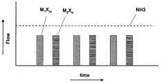
- FIG. 2is a graph illustrating temporally separated metal halide pulses and continuous ammonia flow in accordance with embodiments of the invention
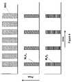
- FIG. 3is a graph illustrating temporally separated metal halide pulses and separate ammonia pulses in accordance with other embodiments of the invention.
- FIG. 4is a graph illustrating simultaneous or mixed metal halide pulses and separate ammonia pulses, in accordance with other embodiments of the invention.
- nitrides of different metalscan be selected for particular applications, such as nitrides continuing Ti, Ta, Hf, Nb, and Mo. Further optimization of film properties can be achieved by using mixtures of two or more nitrides, which has been found particularly beneficial.
- One difficulty in developing a deposition process for such mixed nitridesis finding precursor materials for the respective metals or semiconductors that are compatible with each other.
- the various precursor materialsalthough individually suited to deposit a single nitride, are optimally employed at different deposition temperatures.
- metal-organic precursor materialsare not very thermally stable and often require deposition temperatures below 400° C.
- deposition of mixed nitridescan employ a single wafer reactor to allow control of the deposition process such as described in U.S. Patent Appl. Publication 2004/0009336, published Jan. 14, 2004, wherein TiSiN films are grown using TDMAT, SiH 4 and NH 3 .
- Pulsed CVDflowing NH 3 between halide metal precursor pulses, results is a drastic reduction of the chlorine content in a deposited film compared to a film deposited by regular CVD (in which precursors are not introduced in a plurality of pulses) at the same temperature.
- An advantage of halide metal precursorsis that they are thermally very stable: the halide source materials can be heated to temperatures of several hundred degrees Centigrade, or even to the deposition process temperature without risk of thermal decomposition.
- a second reactantpreferably a nitrogen-containing reactant such as NH 3 , is used to facilitate the chemical reaction.
- two or more metal halide precursors and NH 3are flowed into a reaction chamber for the deposition of a mixed nitride film.
- the NH 3is flowed into the chamber to induce a thermally activated reaction between the NH 3 and at least one metal halide precursor.
- the NH 3is flowed into the chamber to induce a thermally activated reaction between the NH 3 and each of the two metal halide precursors.
- nitrogen precursorssuch as hydrazine (N 2 H 4 )
- N 2 H 4hydrazine
- metalwill be deemed to include Si, Ge and Boron.
- the different metal halide precursorsare generally very compatible and the temperatures required for a reaction with NH 3 are in a similar range: significant reaction rates can be achieved in the temperature range of from about 300° C. to about 700° C., preferably from about 400° C. to about 700° C., more preferably in the range of about 450° C. to about 550° C.
- the processcan further be controlled by flowing the two or more metal halide precursors into the reaction chamber in temporally separated pulses.
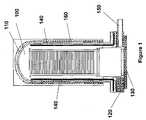
- FIG. 1An exemplary furnace for use with preferred embodiments of the invention is shown in FIG. 1 and commercially available under the trademark A412TM from ASM Europe, The Netherlands.
- a reaction chamber 100is delimited by a process tube 110 , a support flange 120 and a door 130 .
- the process tube 110is closed at the top.
- An advantage of this design in comparison to a design that has a top inlet for gasesis that the process tube 110 is simpler in construction and the problems of gas-tightness and thermal isolation associated with use of a top inlet can be avoided. All gases in this set-up are introduced through gas injectors 140 , of which two are shown. Preferably, separate injectors 140 are used for each gas.
- one injector 140is used for each of the process gases.
- two or more metal halide precursorscan be injected through the same injector or through separate injectors.
- These injectors 140are preferably multiple hole gas injectors having holes distributed over the height of the tube 110 .
- An additional injector 140can be used for a purge gas, preferably an inert gas such as nitrogen gas or a noble gas such as Ar or He.
- the injector 140 for the purge gasis preferably a tube with an open end at its top and without gas discharge holes in its sidewall, so that all the purge gas is discharged near the top of the reaction chamber 100 .
- the gasesare exhausted through an exhaust 150 near the bottom of the reaction chamber 100 .
- the process tubeis surrounded by a heater 160 configured to heat the process chamber to a temperature between 300° C. and 700° C.
- a pulsed CVD process with a gas flow sequence such as schematically depicted in FIG. 2can be used. Temporally separated pulses of two different precursors are fed into the reaction chamber, wherein the first constituent component M 1 of the nitride film is selected from the group of Ti, Zr, Hf, V, Nb, Ta, Cr, Mo, W, and Al and the second constituent component M 2 of the nitride film is selected from the group of Si, Ge, B, Ti, Zr, Hf, V, Nb, Ta, Cr, Mo, W, and Al.
- Xstands for a halide atom.
- the halide ligand atomscan be F, Cl, I or Br or any combination thereof.
- the halideis Cl.
- the precursor pulsesare shown with equal magnitude e.g. equal flow rates. In some embodiments, they may have a different magnitude.
- the subscripts m and nare integer numbers equal to the valence of M 1 and M 2 , typically between 3 and 6.
- the presented formulas for the precursorsare presented as monomeric formulas and the gas phase composition and oxidation state of these precursors can be different, for example, depending upon the temperature. Dimeric, trimeric and more clusterized forms of these precursors might be present in the gas phase and, in some cases, the metal in a precursor can have lower oxidation states.
- a regular alternating sequence of pulsesis shown for M 1 X m and M 2 X n .
- the sequencemay be varied depending on the desired composition of the film, for examply by flowing a first number of sequential pulses of the first metal halide M 1 X m to the reaction chamber and then flowing a second number of sequential pulses of the second metal halide precursor M 2 X n to the reaction chamber.
- the NH 3 flowis continuous and at a constant level during the process.
- the flow rate of the NH 3may also vary during the deposition process.
- the level of the NH 3 flowcan, e.g., be reduced during the metal halide pulses or can even be non-continuous with interruptions in between the metal halide pulses as shown in FIGS. 3 and 4 .
- the NH 3is introduced in temporally separated pulses, as are the metal halides.
- the NH 3 pulses that are provided simultaneously with the metal halide pulsesstart before the start of the metal halide pulse and end after ending of the metal halide pulse to ensure nitrogen precursor presence during deposition.
- the reaction chamberis evacuated.
- an intermediate NH 3 pulseis provided to achieve adequate halide removal and nitrogen incorporation in the deposited film.
- the two different metal halide pulsesare introduced in an alternating manner.
- the two metal halide pulsesoverlap temporally.
- NH 3 pulsesare flowed simultaneously with the metal halide pulses and additional intermediate NH 3 pulses are provided between the metal halide pulses, wherein gases are removed, e.g. by evacuation from the reaction chamber between the NH 3 pulses.
- the evacuation of the reaction chambercan be combined with flowing a purge gas through the reaction chamber.
- a purge gassuch as N 2 or a noble gas can flow during part of the deposition pulses or throughout the process.
- the different metal halide pulsescan over-lap temporally with each other, but the preceding of succeeding pulses remain temporally separated with intervening provision of NH 3 , either in pulses (as shown) or by continuous NH 3 flow (like FIG. 2 ).
- the metal halide precursor and NH 3are simultaneously present within the deposition chamber that houses the substrates, at least during part of the metal halide pulses.
- Flowing the NH 3 during the metal halide pulses and maintaining a deposition temperature between about 300° C. and about 700° C.induces a thermally activated reaction between the metal halide and the NH 3 , resulting in much higher deposition thicknesses than is possible for the alternating pulses used in ALD.
- ALDdue to steric hindrance of the ligands and limited availability of reactive sites, among other things, the deposited thickness per deposition cycle is typically only a small fraction of a monolayer.
- the preferred deposited thickness per deposition cycleis in the range of one full monolayer to a few monolayers.
- the metal and semiconductor precursor materials used for the deposition of mixed nitridesare halides.
- the metalis preferably selected from the group of Ti, Zr, Hf, V, Nb, Ta, Cr, Mo, W, and Al and a semiconductor selected from the group of Si and Ge, with B as a dopant.
- the halidecan be a fluoride, chloride, iodide or bromide or any combination thereof.
- the halideis selected from the group of SiCl 4 , SiHCl 3 , SiH 2 Cl 2 , SiH 3 Cl, GeCl 4 , GeHCl 3 , GeH 2 Cl 2 , GeHCl 3 , BCl 3 , TiCl 4 , ZrCl 4 , HfCl 4 , VCl 5 , TaCl 5 , CrCl 4 , MoCl 5 , MoF 6 , MoF 5 , WCl 5 , WCl 6 , WF 6 AlCl 3 and AlHCl 2 .
- Possible candidates for mixed nitridesare TiSiN, TaSiN, HfSiN, ZrSiN, TiAlN, TaAlN, HfAlN, ZrAlN, TiHfN, TiZrN and HfZrN, preferably TiSiN, TaSiN TiAlN and TiHfN.
- any combination of two or more of the above mentioned metalscan be used.
- TiSiNis formed by pulsed CVD, using TiCl 4 , SiCl 4 and NH 3 as source materials.
- the process conditionsare: process temperature between 450° C. and 550° C., TiCl 4 and SiCl 4 are alternatingly pulsed, TiCl 4 pulse time 30 seconds, SiCl 4 pulse time 30 seconds, interval time between metal precursor pulses 2 minutes, NH 3 flow constant (per FIG. 2 ) at a level of 0.2 slm.
- the deposited thickness per complete cycleis about 1 mm.
- TiSiNis formed by pulsed CVD using TiCl 4 , DCS and NH 3 as source materials.
- the process conditionsare: process temperature between 450° C. and 550° C., TiCl 4 and DCS are alternatingly pulsed, TiCl 4 pulse time 30 seconds, DCS pulse time 30 seconds, interval time between metal precursor pulses 2 minutes, NH 3 flow constant (per FIG. 2 ) at a level of 0.2 slm.
- the deposited thickness per complete cycleis about 1 nm.
- TiAlNis formed by pulsed CVD using TiCl 4 , AlCl 3 and NH 3 as source materials.
- TMAis by far the most commonly used aluminum source material for deposition of aluminum-containing films
- AlCl 3is an easily available alternative with relatively high vapor pressure of 1 Torr at 100° C. and a AlCl 3 container temperature between 100° C. and 130° C. is sufficient to be able to generate source material pulses that are adequate for a batch system.
- the process settingsare: process temperature between 450° C.
- TiCl 4 and AlCl 3are alternatingly pulsed, TiCl 4 pulse time 30 seconds, AlCl 3 pulse time 30 seconds, interval time between metal precursor pulses 2 minutes, NH 3 flow constant (per FIG. 2 ) at a level of 0.2 slm.
- a precursor dosing rate in the range between 1 and 10 g/minuteis adequate, preferably the dosing rate is about 5 g/minute.
- the estimated deposited thickness per complete cycleis about 1 nm.
- TiSiNis formed by pulsed CVD using TiCl 4 , DCS and NH 3 as source materials.
- the use of DCS in combination with TiCl 4is particularly beneficial as, when introduced simultaneously (per FIG. 4 ), the DCS can reduce the Ti(IV) to Ti(III) which is the most difficult step of the chemical reactions involving TiCl 4 .
- the process conditionsare: process temperature between 450° C. and 550° C., TiCl 4 and DCS are simultaneously pulsed (per FIG. 4 ), pulse time 30 seconds, interval time between metal precursor pulses 3 minutes, NH 3 flow pulsed (per FIG.
- the deposited thickness per complete cycleis about 1 nm.
- a chlorine removing agentcan be flowed into the reaction chamber.
- Such an agentcan be flowed into the reaction chamber in a continuous manner or in temporally separated pulses.
- suitable chlorine removing agentsare carbon chains comprising a double carbon-carbon bond (alkenes), such as ethane (C 2 H 4 ), propene (C 3 H 6 ) and butane (C 4 H 8 ), or triple carbon-carbon bonds, such as ethyne, (C 2 H 2 ), propyne (C 3 H 4 ), and buthyne (C 4 H 6 ).
- Ring-structured carbon chainslike benzene, cyclohepthene, or cyclopentadienyl that have at least one double bond can also be used.
- the double bondcan break open and each carbon dangling bond can connect to a chlorine atom.
Landscapes
- Chemical & Material Sciences (AREA)
- General Chemical & Material Sciences (AREA)
- Chemical Kinetics & Catalysis (AREA)
- Engineering & Computer Science (AREA)
- Materials Engineering (AREA)
- Mechanical Engineering (AREA)
- Metallurgy (AREA)
- Organic Chemistry (AREA)
- Inorganic Chemistry (AREA)
- Chemical Vapour Deposition (AREA)
Abstract
Description
Claims (16)
Priority Applications (1)
| Application Number | Priority Date | Filing Date | Title |
|---|---|---|---|
| US11/766,718US7691757B2 (en) | 2006-06-22 | 2007-06-21 | Deposition of complex nitride films |
Applications Claiming Priority (2)
| Application Number | Priority Date | Filing Date | Title |
|---|---|---|---|
| US81610406P | 2006-06-22 | 2006-06-22 | |
| US11/766,718US7691757B2 (en) | 2006-06-22 | 2007-06-21 | Deposition of complex nitride films |
Publications (2)
| Publication Number | Publication Date |
|---|---|
| US20080003838A1 US20080003838A1 (en) | 2008-01-03 |
| US7691757B2true US7691757B2 (en) | 2010-04-06 |
Family
ID=38877256
Family Applications (1)
| Application Number | Title | Priority Date | Filing Date |
|---|---|---|---|
| US11/766,718Active2027-11-25US7691757B2 (en) | 2006-06-22 | 2007-06-21 | Deposition of complex nitride films |
Country Status (1)
| Country | Link |
|---|---|
| US (1) | US7691757B2 (en) |
Cited By (8)
| Publication number | Priority date | Publication date | Assignee | Title |
|---|---|---|---|---|
| US20080317972A1 (en)* | 2007-06-21 | 2008-12-25 | Asm International N.V. | Method for depositing thin films by mixed pulsed cvd and ald |
| US20100210067A1 (en)* | 2009-02-11 | 2010-08-19 | Kenneth Scott Alexander Butcher | Migration and plasma enhanced chemical vapor deposition |
| US8143147B1 (en) | 2011-02-10 | 2012-03-27 | Intermolecular, Inc. | Methods and systems for forming thin films |
| US10170321B2 (en) | 2017-03-17 | 2019-01-01 | Applied Materials, Inc. | Aluminum content control of TiAIN films |
| US20200318237A1 (en)* | 2019-04-05 | 2020-10-08 | Asm Ip Holding B.V. | Methods for forming a boron nitride film by a plasma enhanced atomic layer deposition process |
| US10978552B2 (en) | 2018-05-18 | 2021-04-13 | Samsung Electronics Co., Ltd. | Semiconductor devices and method of manufacturing the same |
| US11299807B2 (en)* | 2017-09-29 | 2022-04-12 | Mitsubishi Materials Corporation | Surface-coated cutting tool in which hard coating layer exhibits exceptional adhesion resistance and anomalous damage resistance |
| US20230352556A1 (en)* | 2017-07-18 | 2023-11-02 | Asm Ip Holding B.V. | Methods for forming a semiconductor device structure and related semiconductor device structures |
Families Citing this family (401)
| Publication number | Priority date | Publication date | Assignee | Title |
|---|---|---|---|---|
| US7966969B2 (en) | 2004-09-22 | 2011-06-28 | Asm International N.V. | Deposition of TiN films in a batch reactor |
| US7629256B2 (en) | 2007-05-14 | 2009-12-08 | Asm International N.V. | In situ silicon and titanium nitride deposition |
| KR101308130B1 (en)* | 2008-03-25 | 2013-09-12 | 서울옵토디바이스주식회사 | Light emitting device and method for fabricating the same |
| KR101576033B1 (en) | 2008-08-19 | 2015-12-11 | 삼성전자주식회사 | Precursor composition, thin film forming method, manufacturing method of gate structure using same, and manufacturing method of capacitor |
| US10378106B2 (en) | 2008-11-14 | 2019-08-13 | Asm Ip Holding B.V. | Method of forming insulation film by modified PEALD |
| US7833906B2 (en) | 2008-12-11 | 2010-11-16 | Asm International N.V. | Titanium silicon nitride deposition |
| US7972980B2 (en)* | 2009-01-21 | 2011-07-05 | Asm Japan K.K. | Method of forming conformal dielectric film having Si-N bonds by PECVD |
| US8142862B2 (en)* | 2009-01-21 | 2012-03-27 | Asm Japan K.K. | Method of forming conformal dielectric film having Si-N bonds by PECVD |
| US7919416B2 (en)* | 2009-01-21 | 2011-04-05 | Asm Japan K.K. | Method of forming conformal dielectric film having Si-N bonds by PECVD |
| US9394608B2 (en) | 2009-04-06 | 2016-07-19 | Asm America, Inc. | Semiconductor processing reactor and components thereof |
| US8802201B2 (en) | 2009-08-14 | 2014-08-12 | Asm America, Inc. | Systems and methods for thin-film deposition of metal oxides using excited nitrogen-oxygen species |
| US8563085B2 (en)* | 2009-08-18 | 2013-10-22 | Samsung Electronics Co., Ltd. | Precursor composition, methods of forming a layer, methods of forming a gate structure and methods of forming a capacitor |
| US20110045183A1 (en)* | 2009-08-18 | 2011-02-24 | Youn-Joung Cho | Methods of forming a layer, methods of forming a gate structure and methods of forming a capacitor |
| KR20110133241A (en) | 2010-06-04 | 2011-12-12 | 서울옵토디바이스주식회사 | Light emitting diode manufacturing method |
| US8524322B2 (en) | 2010-12-28 | 2013-09-03 | Asm International N.V. | Combination CVD/ALD method and source |
| US9790594B2 (en) | 2010-12-28 | 2017-10-17 | Asm Ip Holding B.V. | Combination CVD/ALD method, source and pulse profile modification |
| US9312155B2 (en) | 2011-06-06 | 2016-04-12 | Asm Japan K.K. | High-throughput semiconductor-processing apparatus equipped with multiple dual-chamber modules |
| US9793148B2 (en) | 2011-06-22 | 2017-10-17 | Asm Japan K.K. | Method for positioning wafers in multiple wafer transport |
| US10364496B2 (en) | 2011-06-27 | 2019-07-30 | Asm Ip Holding B.V. | Dual section module having shared and unshared mass flow controllers |
| US10854498B2 (en) | 2011-07-15 | 2020-12-01 | Asm Ip Holding B.V. | Wafer-supporting device and method for producing same |
| US20130023129A1 (en) | 2011-07-20 | 2013-01-24 | Asm America, Inc. | Pressure transmitter for a semiconductor processing environment |
| US9017481B1 (en) | 2011-10-28 | 2015-04-28 | Asm America, Inc. | Process feed management for semiconductor substrate processing |
| US8927059B2 (en)* | 2011-11-08 | 2015-01-06 | Applied Materials, Inc. | Deposition of metal films using alane-based precursors |
| US8946830B2 (en) | 2012-04-04 | 2015-02-03 | Asm Ip Holdings B.V. | Metal oxide protective layer for a semiconductor device |
| US9558931B2 (en) | 2012-07-27 | 2017-01-31 | Asm Ip Holding B.V. | System and method for gas-phase sulfur passivation of a semiconductor surface |
| US9659799B2 (en) | 2012-08-28 | 2017-05-23 | Asm Ip Holding B.V. | Systems and methods for dynamic semiconductor process scheduling |
| US9021985B2 (en) | 2012-09-12 | 2015-05-05 | Asm Ip Holdings B.V. | Process gas management for an inductively-coupled plasma deposition reactor |
| US9324811B2 (en) | 2012-09-26 | 2016-04-26 | Asm Ip Holding B.V. | Structures and devices including a tensile-stressed silicon arsenic layer and methods of forming same |
| US10714315B2 (en) | 2012-10-12 | 2020-07-14 | Asm Ip Holdings B.V. | Semiconductor reaction chamber showerhead |
| US9640416B2 (en) | 2012-12-26 | 2017-05-02 | Asm Ip Holding B.V. | Single-and dual-chamber module-attachable wafer-handling chamber |
| US20160376700A1 (en) | 2013-02-01 | 2016-12-29 | Asm Ip Holding B.V. | System for treatment of deposition reactor |
| US9484191B2 (en) | 2013-03-08 | 2016-11-01 | Asm Ip Holding B.V. | Pulsed remote plasma method and system |
| US9589770B2 (en) | 2013-03-08 | 2017-03-07 | Asm Ip Holding B.V. | Method and systems for in-situ formation of intermediate reactive species |
| US8993054B2 (en) | 2013-07-12 | 2015-03-31 | Asm Ip Holding B.V. | Method and system to reduce outgassing in a reaction chamber |
| US9018111B2 (en) | 2013-07-22 | 2015-04-28 | Asm Ip Holding B.V. | Semiconductor reaction chamber with plasma capabilities |
| US9793115B2 (en) | 2013-08-14 | 2017-10-17 | Asm Ip Holding B.V. | Structures and devices including germanium-tin films and methods of forming same |
| US9240412B2 (en) | 2013-09-27 | 2016-01-19 | Asm Ip Holding B.V. | Semiconductor structure and device and methods of forming same using selective epitaxial process |
| US9556516B2 (en) | 2013-10-09 | 2017-01-31 | ASM IP Holding B.V | Method for forming Ti-containing film by PEALD using TDMAT or TDEAT |
| US10179947B2 (en) | 2013-11-26 | 2019-01-15 | Asm Ip Holding B.V. | Method for forming conformal nitrided, oxidized, or carbonized dielectric film by atomic layer deposition |
| US10683571B2 (en) | 2014-02-25 | 2020-06-16 | Asm Ip Holding B.V. | Gas supply manifold and method of supplying gases to chamber using same |
| US10167557B2 (en) | 2014-03-18 | 2019-01-01 | Asm Ip Holding B.V. | Gas distribution system, reactor including the system, and methods of using the same |
| US9447498B2 (en) | 2014-03-18 | 2016-09-20 | Asm Ip Holding B.V. | Method for performing uniform processing in gas system-sharing multiple reaction chambers |
| US11015245B2 (en) | 2014-03-19 | 2021-05-25 | Asm Ip Holding B.V. | Gas-phase reactor and system having exhaust plenum and components thereof |
| US9404587B2 (en) | 2014-04-24 | 2016-08-02 | ASM IP Holding B.V | Lockout tagout for semiconductor vacuum valve |
| US10858737B2 (en) | 2014-07-28 | 2020-12-08 | Asm Ip Holding B.V. | Showerhead assembly and components thereof |
| US9543180B2 (en) | 2014-08-01 | 2017-01-10 | Asm Ip Holding B.V. | Apparatus and method for transporting wafers between wafer carrier and process tool under vacuum |
| US9890456B2 (en) | 2014-08-21 | 2018-02-13 | Asm Ip Holding B.V. | Method and system for in situ formation of gas-phase compounds |
| US9657845B2 (en) | 2014-10-07 | 2017-05-23 | Asm Ip Holding B.V. | Variable conductance gas distribution apparatus and method |
| US10941490B2 (en) | 2014-10-07 | 2021-03-09 | Asm Ip Holding B.V. | Multiple temperature range susceptor, assembly, reactor and system including the susceptor, and methods of using the same |
| KR102300403B1 (en) | 2014-11-19 | 2021-09-09 | 에이에스엠 아이피 홀딩 비.브이. | Method of depositing thin film |
| KR102263121B1 (en) | 2014-12-22 | 2021-06-09 | 에이에스엠 아이피 홀딩 비.브이. | Semiconductor device and manufacuring method thereof |
| US9478415B2 (en) | 2015-02-13 | 2016-10-25 | Asm Ip Holding B.V. | Method for forming film having low resistance and shallow junction depth |
| US10529542B2 (en) | 2015-03-11 | 2020-01-07 | Asm Ip Holdings B.V. | Cross-flow reactor and method |
| US10276355B2 (en) | 2015-03-12 | 2019-04-30 | Asm Ip Holding B.V. | Multi-zone reactor, system including the reactor, and method of using the same |
| US10458018B2 (en) | 2015-06-26 | 2019-10-29 | Asm Ip Holding B.V. | Structures including metal carbide material, devices including the structures, and methods of forming same |
| US10600673B2 (en) | 2015-07-07 | 2020-03-24 | Asm Ip Holding B.V. | Magnetic susceptor to baseplate seal |
| US10043661B2 (en) | 2015-07-13 | 2018-08-07 | Asm Ip Holding B.V. | Method for protecting layer by forming hydrocarbon-based extremely thin film |
| US9899291B2 (en) | 2015-07-13 | 2018-02-20 | Asm Ip Holding B.V. | Method for protecting layer by forming hydrocarbon-based extremely thin film |
| US10083836B2 (en) | 2015-07-24 | 2018-09-25 | Asm Ip Holding B.V. | Formation of boron-doped titanium metal films with high work function |
| US10087525B2 (en) | 2015-08-04 | 2018-10-02 | Asm Ip Holding B.V. | Variable gap hard stop design |
| US9647114B2 (en) | 2015-08-14 | 2017-05-09 | Asm Ip Holding B.V. | Methods of forming highly p-type doped germanium tin films and structures and devices including the films |
| US9711345B2 (en) | 2015-08-25 | 2017-07-18 | Asm Ip Holding B.V. | Method for forming aluminum nitride-based film by PEALD |
| JP6486479B2 (en)* | 2015-09-03 | 2019-03-20 | 株式会社Kokusai Electric | Semiconductor device manufacturing method, substrate processing apparatus, program, and supply system |
| US9960072B2 (en) | 2015-09-29 | 2018-05-01 | Asm Ip Holding B.V. | Variable adjustment for precise matching of multiple chamber cavity housings |
| US9909214B2 (en) | 2015-10-15 | 2018-03-06 | Asm Ip Holding B.V. | Method for depositing dielectric film in trenches by PEALD |
| US10211308B2 (en) | 2015-10-21 | 2019-02-19 | Asm Ip Holding B.V. | NbMC layers |
| US10322384B2 (en) | 2015-11-09 | 2019-06-18 | Asm Ip Holding B.V. | Counter flow mixer for process chamber |
| US9455138B1 (en) | 2015-11-10 | 2016-09-27 | Asm Ip Holding B.V. | Method for forming dielectric film in trenches by PEALD using H-containing gas |
| US9905420B2 (en) | 2015-12-01 | 2018-02-27 | Asm Ip Holding B.V. | Methods of forming silicon germanium tin films and structures and devices including the films |
| US9607837B1 (en) | 2015-12-21 | 2017-03-28 | Asm Ip Holding B.V. | Method for forming silicon oxide cap layer for solid state diffusion process |
| US9627221B1 (en) | 2015-12-28 | 2017-04-18 | Asm Ip Holding B.V. | Continuous process incorporating atomic layer etching |
| US9735024B2 (en) | 2015-12-28 | 2017-08-15 | Asm Ip Holding B.V. | Method of atomic layer etching using functional group-containing fluorocarbon |
| US11139308B2 (en) | 2015-12-29 | 2021-10-05 | Asm Ip Holding B.V. | Atomic layer deposition of III-V compounds to form V-NAND devices |
| US10529554B2 (en) | 2016-02-19 | 2020-01-07 | Asm Ip Holding B.V. | Method for forming silicon nitride film selectively on sidewalls or flat surfaces of trenches |
| US9754779B1 (en) | 2016-02-19 | 2017-09-05 | Asm Ip Holding B.V. | Method for forming silicon nitride film selectively on sidewalls or flat surfaces of trenches |
| US10468251B2 (en) | 2016-02-19 | 2019-11-05 | Asm Ip Holding B.V. | Method for forming spacers using silicon nitride film for spacer-defined multiple patterning |
| US10501866B2 (en) | 2016-03-09 | 2019-12-10 | Asm Ip Holding B.V. | Gas distribution apparatus for improved film uniformity in an epitaxial system |
| US10343920B2 (en) | 2016-03-18 | 2019-07-09 | Asm Ip Holding B.V. | Aligned carbon nanotubes |
| US9892913B2 (en) | 2016-03-24 | 2018-02-13 | Asm Ip Holding B.V. | Radial and thickness control via biased multi-port injection settings |
| US10190213B2 (en) | 2016-04-21 | 2019-01-29 | Asm Ip Holding B.V. | Deposition of metal borides |
| US10087522B2 (en) | 2016-04-21 | 2018-10-02 | Asm Ip Holding B.V. | Deposition of metal borides |
| US10865475B2 (en) | 2016-04-21 | 2020-12-15 | Asm Ip Holding B.V. | Deposition of metal borides and silicides |
| US10367080B2 (en) | 2016-05-02 | 2019-07-30 | Asm Ip Holding B.V. | Method of forming a germanium oxynitride film |
| US10032628B2 (en) | 2016-05-02 | 2018-07-24 | Asm Ip Holding B.V. | Source/drain performance through conformal solid state doping |
| KR102592471B1 (en) | 2016-05-17 | 2023-10-20 | 에이에스엠 아이피 홀딩 비.브이. | Method of forming metal interconnection and method of fabricating semiconductor device using the same |
| US11453943B2 (en) | 2016-05-25 | 2022-09-27 | Asm Ip Holding B.V. | Method for forming carbon-containing silicon/metal oxide or nitride film by ALD using silicon precursor and hydrocarbon precursor |
| US10388509B2 (en) | 2016-06-28 | 2019-08-20 | Asm Ip Holding B.V. | Formation of epitaxial layers via dislocation filtering |
| US9859151B1 (en) | 2016-07-08 | 2018-01-02 | Asm Ip Holding B.V. | Selective film deposition method to form air gaps |
| US10612137B2 (en) | 2016-07-08 | 2020-04-07 | Asm Ip Holdings B.V. | Organic reactants for atomic layer deposition |
| US9793135B1 (en) | 2016-07-14 | 2017-10-17 | ASM IP Holding B.V | Method of cyclic dry etching using etchant film |
| US10714385B2 (en) | 2016-07-19 | 2020-07-14 | Asm Ip Holding B.V. | Selective deposition of tungsten |
| KR102354490B1 (en) | 2016-07-27 | 2022-01-21 | 에이에스엠 아이피 홀딩 비.브이. | Method of processing a substrate |
| US10177025B2 (en) | 2016-07-28 | 2019-01-08 | Asm Ip Holding B.V. | Method and apparatus for filling a gap |
| US10395919B2 (en) | 2016-07-28 | 2019-08-27 | Asm Ip Holding B.V. | Method and apparatus for filling a gap |
| US9812320B1 (en) | 2016-07-28 | 2017-11-07 | Asm Ip Holding B.V. | Method and apparatus for filling a gap |
| KR102532607B1 (en) | 2016-07-28 | 2023-05-15 | 에이에스엠 아이피 홀딩 비.브이. | Substrate processing apparatus and method of operating the same |
| US9887082B1 (en) | 2016-07-28 | 2018-02-06 | Asm Ip Holding B.V. | Method and apparatus for filling a gap |
| US10090316B2 (en) | 2016-09-01 | 2018-10-02 | Asm Ip Holding B.V. | 3D stacked multilayer semiconductor memory using doped select transistor channel |
| US10410943B2 (en) | 2016-10-13 | 2019-09-10 | Asm Ip Holding B.V. | Method for passivating a surface of a semiconductor and related systems |
| US10643826B2 (en) | 2016-10-26 | 2020-05-05 | Asm Ip Holdings B.V. | Methods for thermally calibrating reaction chambers |
| US10714350B2 (en) | 2016-11-01 | 2020-07-14 | ASM IP Holdings, B.V. | Methods for forming a transition metal niobium nitride film on a substrate by atomic layer deposition and related semiconductor device structures |
| US10229833B2 (en) | 2016-11-01 | 2019-03-12 | Asm Ip Holding B.V. | Methods for forming a transition metal nitride film on a substrate by atomic layer deposition and related semiconductor device structures |
| US10435790B2 (en) | 2016-11-01 | 2019-10-08 | Asm Ip Holding B.V. | Method of subatmospheric plasma-enhanced ALD using capacitively coupled electrodes with narrow gap |
| US10643904B2 (en) | 2016-11-01 | 2020-05-05 | Asm Ip Holdings B.V. | Methods for forming a semiconductor device and related semiconductor device structures |
| US10134757B2 (en) | 2016-11-07 | 2018-11-20 | Asm Ip Holding B.V. | Method of processing a substrate and a device manufactured by using the method |
| KR102546317B1 (en) | 2016-11-15 | 2023-06-21 | 에이에스엠 아이피 홀딩 비.브이. | Gas supply unit and substrate processing apparatus including the same |
| US10340135B2 (en) | 2016-11-28 | 2019-07-02 | Asm Ip Holding B.V. | Method of topologically restricted plasma-enhanced cyclic deposition of silicon or metal nitride |
| KR102762543B1 (en) | 2016-12-14 | 2025-02-05 | 에이에스엠 아이피 홀딩 비.브이. | Substrate processing apparatus |
| US11581186B2 (en) | 2016-12-15 | 2023-02-14 | Asm Ip Holding B.V. | Sequential infiltration synthesis apparatus |
| US11447861B2 (en) | 2016-12-15 | 2022-09-20 | Asm Ip Holding B.V. | Sequential infiltration synthesis apparatus and a method of forming a patterned structure |
| US9916980B1 (en) | 2016-12-15 | 2018-03-13 | Asm Ip Holding B.V. | Method of forming a structure on a substrate |
| KR102700194B1 (en) | 2016-12-19 | 2024-08-28 | 에이에스엠 아이피 홀딩 비.브이. | Substrate processing apparatus |
| US10269558B2 (en) | 2016-12-22 | 2019-04-23 | Asm Ip Holding B.V. | Method of forming a structure on a substrate |
| US10867788B2 (en) | 2016-12-28 | 2020-12-15 | Asm Ip Holding B.V. | Method of forming a structure on a substrate |
| US11390950B2 (en) | 2017-01-10 | 2022-07-19 | Asm Ip Holding B.V. | Reactor system and method to reduce residue buildup during a film deposition process |
| US10655221B2 (en) | 2017-02-09 | 2020-05-19 | Asm Ip Holding B.V. | Method for depositing oxide film by thermal ALD and PEALD |
| US10468261B2 (en) | 2017-02-15 | 2019-11-05 | Asm Ip Holding B.V. | Methods for forming a metallic film on a substrate by cyclical deposition and related semiconductor device structures |
| US10529563B2 (en) | 2017-03-29 | 2020-01-07 | Asm Ip Holdings B.V. | Method for forming doped metal oxide films on a substrate by cyclical deposition and related semiconductor device structures |
| US10283353B2 (en) | 2017-03-29 | 2019-05-07 | Asm Ip Holding B.V. | Method of reforming insulating film deposited on substrate with recess pattern |
| US10103040B1 (en) | 2017-03-31 | 2018-10-16 | Asm Ip Holding B.V. | Apparatus and method for manufacturing a semiconductor device |
| USD830981S1 (en) | 2017-04-07 | 2018-10-16 | Asm Ip Holding B.V. | Susceptor for semiconductor substrate processing apparatus |
| KR102457289B1 (en) | 2017-04-25 | 2022-10-21 | 에이에스엠 아이피 홀딩 비.브이. | Method for depositing a thin film and manufacturing a semiconductor device |
| US10446393B2 (en) | 2017-05-08 | 2019-10-15 | Asm Ip Holding B.V. | Methods for forming silicon-containing epitaxial layers and related semiconductor device structures |
| US10770286B2 (en) | 2017-05-08 | 2020-09-08 | Asm Ip Holdings B.V. | Methods for selectively forming a silicon nitride film on a substrate and related semiconductor device structures |
| US10892156B2 (en) | 2017-05-08 | 2021-01-12 | Asm Ip Holding B.V. | Methods for forming a silicon nitride film on a substrate and related semiconductor device structures |
| US10504742B2 (en) | 2017-05-31 | 2019-12-10 | Asm Ip Holding B.V. | Method of atomic layer etching using hydrogen plasma |
| US10886123B2 (en) | 2017-06-02 | 2021-01-05 | Asm Ip Holding B.V. | Methods for forming low temperature semiconductor layers and related semiconductor device structures |
| US12040200B2 (en) | 2017-06-20 | 2024-07-16 | Asm Ip Holding B.V. | Semiconductor processing apparatus and methods for calibrating a semiconductor processing apparatus |
| US11306395B2 (en) | 2017-06-28 | 2022-04-19 | Asm Ip Holding B.V. | Methods for depositing a transition metal nitride film on a substrate by atomic layer deposition and related deposition apparatus |
| US10685834B2 (en) | 2017-07-05 | 2020-06-16 | Asm Ip Holdings B.V. | Methods for forming a silicon germanium tin layer and related semiconductor device structures |
| US11018002B2 (en) | 2017-07-19 | 2021-05-25 | Asm Ip Holding B.V. | Method for selectively depositing a Group IV semiconductor and related semiconductor device structures |
| US11374112B2 (en) | 2017-07-19 | 2022-06-28 | Asm Ip Holding B.V. | Method for depositing a group IV semiconductor and related semiconductor device structures |
| US10541333B2 (en) | 2017-07-19 | 2020-01-21 | Asm Ip Holding B.V. | Method for depositing a group IV semiconductor and related semiconductor device structures |
| US10312055B2 (en) | 2017-07-26 | 2019-06-04 | Asm Ip Holding B.V. | Method of depositing film by PEALD using negative bias |
| US10590535B2 (en) | 2017-07-26 | 2020-03-17 | Asm Ip Holdings B.V. | Chemical treatment, deposition and/or infiltration apparatus and method for using the same |
| US10605530B2 (en) | 2017-07-26 | 2020-03-31 | Asm Ip Holding B.V. | Assembly of a liner and a flange for a vertical furnace as well as the liner and the vertical furnace |
| TWI815813B (en) | 2017-08-04 | 2023-09-21 | 荷蘭商Asm智慧財產控股公司 | Showerhead assembly for distributing a gas within a reaction chamber |
| US10770336B2 (en) | 2017-08-08 | 2020-09-08 | Asm Ip Holding B.V. | Substrate lift mechanism and reactor including same |
| US10692741B2 (en) | 2017-08-08 | 2020-06-23 | Asm Ip Holdings B.V. | Radiation shield |
| US11769682B2 (en) | 2017-08-09 | 2023-09-26 | Asm Ip Holding B.V. | Storage apparatus for storing cassettes for substrates and processing apparatus equipped therewith |
| US11139191B2 (en) | 2017-08-09 | 2021-10-05 | Asm Ip Holding B.V. | Storage apparatus for storing cassettes for substrates and processing apparatus equipped therewith |
| US10249524B2 (en) | 2017-08-09 | 2019-04-02 | Asm Ip Holding B.V. | Cassette holder assembly for a substrate cassette and holding member for use in such assembly |
| US10236177B1 (en) | 2017-08-22 | 2019-03-19 | ASM IP Holding B.V.. | Methods for depositing a doped germanium tin semiconductor and related semiconductor device structures |
| USD900036S1 (en) | 2017-08-24 | 2020-10-27 | Asm Ip Holding B.V. | Heater electrical connector and adapter |
| US11830730B2 (en) | 2017-08-29 | 2023-11-28 | Asm Ip Holding B.V. | Layer forming method and apparatus |
| KR102491945B1 (en) | 2017-08-30 | 2023-01-26 | 에이에스엠 아이피 홀딩 비.브이. | Substrate processing apparatus |
| US11295980B2 (en) | 2017-08-30 | 2022-04-05 | Asm Ip Holding B.V. | Methods for depositing a molybdenum metal film over a dielectric surface of a substrate by a cyclical deposition process and related semiconductor device structures |
| US11056344B2 (en) | 2017-08-30 | 2021-07-06 | Asm Ip Holding B.V. | Layer forming method |
| KR102401446B1 (en) | 2017-08-31 | 2022-05-24 | 에이에스엠 아이피 홀딩 비.브이. | Substrate processing apparatus |
| US10607895B2 (en) | 2017-09-18 | 2020-03-31 | Asm Ip Holdings B.V. | Method for forming a semiconductor device structure comprising a gate fill metal |
| KR102630301B1 (en) | 2017-09-21 | 2024-01-29 | 에이에스엠 아이피 홀딩 비.브이. | Method of sequential infiltration synthesis treatment of infiltrateable material and structures and devices formed using same |
| US10844484B2 (en) | 2017-09-22 | 2020-11-24 | Asm Ip Holding B.V. | Apparatus for dispensing a vapor phase reactant to a reaction chamber and related methods |
| US10658205B2 (en) | 2017-09-28 | 2020-05-19 | Asm Ip Holdings B.V. | Chemical dispensing apparatus and methods for dispensing a chemical to a reaction chamber |
| US10403504B2 (en) | 2017-10-05 | 2019-09-03 | Asm Ip Holding B.V. | Method for selectively depositing a metallic film on a substrate |
| US10319588B2 (en) | 2017-10-10 | 2019-06-11 | Asm Ip Holding B.V. | Method for depositing a metal chalcogenide on a substrate by cyclical deposition |
| US10923344B2 (en) | 2017-10-30 | 2021-02-16 | Asm Ip Holding B.V. | Methods for forming a semiconductor structure and related semiconductor structures |
| KR102443047B1 (en) | 2017-11-16 | 2022-09-14 | 에이에스엠 아이피 홀딩 비.브이. | Method of processing a substrate and a device manufactured by the same |
| US10910262B2 (en) | 2017-11-16 | 2021-02-02 | Asm Ip Holding B.V. | Method of selectively depositing a capping layer structure on a semiconductor device structure |
| US11022879B2 (en) | 2017-11-24 | 2021-06-01 | Asm Ip Holding B.V. | Method of forming an enhanced unexposed photoresist layer |
| WO2019103613A1 (en) | 2017-11-27 | 2019-05-31 | Asm Ip Holding B.V. | A storage device for storing wafer cassettes for use with a batch furnace |
| CN111344522B (en) | 2017-11-27 | 2022-04-12 | 阿斯莫Ip控股公司 | Including clean mini-environment device |
| US10290508B1 (en) | 2017-12-05 | 2019-05-14 | Asm Ip Holding B.V. | Method for forming vertical spacers for spacer-defined patterning |
| US10872771B2 (en) | 2018-01-16 | 2020-12-22 | Asm Ip Holding B. V. | Method for depositing a material film on a substrate within a reaction chamber by a cyclical deposition process and related device structures |
| TWI799494B (en) | 2018-01-19 | 2023-04-21 | 荷蘭商Asm 智慧財產控股公司 | Deposition method |
| KR102695659B1 (en) | 2018-01-19 | 2024-08-14 | 에이에스엠 아이피 홀딩 비.브이. | Method for depositing a gap filling layer by plasma assisted deposition |
| USD903477S1 (en) | 2018-01-24 | 2020-12-01 | Asm Ip Holdings B.V. | Metal clamp |
| US11018047B2 (en) | 2018-01-25 | 2021-05-25 | Asm Ip Holding B.V. | Hybrid lift pin |
| US10535516B2 (en) | 2018-02-01 | 2020-01-14 | Asm Ip Holdings B.V. | Method for depositing a semiconductor structure on a surface of a substrate and related semiconductor structures |
| USD880437S1 (en) | 2018-02-01 | 2020-04-07 | Asm Ip Holding B.V. | Gas supply plate for semiconductor manufacturing apparatus |
| US11081345B2 (en) | 2018-02-06 | 2021-08-03 | Asm Ip Holding B.V. | Method of post-deposition treatment for silicon oxide film |
| US10896820B2 (en) | 2018-02-14 | 2021-01-19 | Asm Ip Holding B.V. | Method for depositing a ruthenium-containing film on a substrate by a cyclical deposition process |
| WO2019158960A1 (en) | 2018-02-14 | 2019-08-22 | Asm Ip Holding B.V. | A method for depositing a ruthenium-containing film on a substrate by a cyclical deposition process |
| US10731249B2 (en) | 2018-02-15 | 2020-08-04 | Asm Ip Holding B.V. | Method of forming a transition metal containing film on a substrate by a cyclical deposition process, a method for supplying a transition metal halide compound to a reaction chamber, and related vapor deposition apparatus |
| US10658181B2 (en) | 2018-02-20 | 2020-05-19 | Asm Ip Holding B.V. | Method of spacer-defined direct patterning in semiconductor fabrication |
| KR102636427B1 (en) | 2018-02-20 | 2024-02-13 | 에이에스엠 아이피 홀딩 비.브이. | Substrate processing method and apparatus |
| US10975470B2 (en) | 2018-02-23 | 2021-04-13 | Asm Ip Holding B.V. | Apparatus for detecting or monitoring for a chemical precursor in a high temperature environment |
| US11473195B2 (en) | 2018-03-01 | 2022-10-18 | Asm Ip Holding B.V. | Semiconductor processing apparatus and a method for processing a substrate |
| US11629406B2 (en) | 2018-03-09 | 2023-04-18 | Asm Ip Holding B.V. | Semiconductor processing apparatus comprising one or more pyrometers for measuring a temperature of a substrate during transfer of the substrate |
| US11114283B2 (en) | 2018-03-16 | 2021-09-07 | Asm Ip Holding B.V. | Reactor, system including the reactor, and methods of manufacturing and using same |
| KR102646467B1 (en) | 2018-03-27 | 2024-03-11 | 에이에스엠 아이피 홀딩 비.브이. | Method of forming an electrode on a substrate and a semiconductor device structure including an electrode |
| US11230766B2 (en) | 2018-03-29 | 2022-01-25 | Asm Ip Holding B.V. | Substrate processing apparatus and method |
| US10510536B2 (en) | 2018-03-29 | 2019-12-17 | Asm Ip Holding B.V. | Method of depositing a co-doped polysilicon film on a surface of a substrate within a reaction chamber |
| US11088002B2 (en) | 2018-03-29 | 2021-08-10 | Asm Ip Holding B.V. | Substrate rack and a substrate processing system and method |
| KR102501472B1 (en) | 2018-03-30 | 2023-02-20 | 에이에스엠 아이피 홀딩 비.브이. | Substrate processing method |
| KR102600229B1 (en) | 2018-04-09 | 2023-11-10 | 에이에스엠 아이피 홀딩 비.브이. | Substrate supporting device, substrate processing apparatus including the same and substrate processing method |
| TWI811348B (en) | 2018-05-08 | 2023-08-11 | 荷蘭商Asm 智慧財產控股公司 | Methods for depositing an oxide film on a substrate by a cyclical deposition process and related device structures |
| US12025484B2 (en) | 2018-05-08 | 2024-07-02 | Asm Ip Holding B.V. | Thin film forming method |
| US12272527B2 (en) | 2018-05-09 | 2025-04-08 | Asm Ip Holding B.V. | Apparatus for use with hydrogen radicals and method of using same |
| KR20190129718A (en) | 2018-05-11 | 2019-11-20 | 에이에스엠 아이피 홀딩 비.브이. | Methods for forming a doped metal carbide film on a substrate and related semiconductor device structures |
| KR102596988B1 (en) | 2018-05-28 | 2023-10-31 | 에이에스엠 아이피 홀딩 비.브이. | Method of processing a substrate and a device manufactured by the same |
| US11718913B2 (en) | 2018-06-04 | 2023-08-08 | Asm Ip Holding B.V. | Gas distribution system and reactor system including same |
| TWI840362B (en) | 2018-06-04 | 2024-05-01 | 荷蘭商Asm Ip私人控股有限公司 | Wafer handling chamber with moisture reduction |
| US11286562B2 (en) | 2018-06-08 | 2022-03-29 | Asm Ip Holding B.V. | Gas-phase chemical reactor and method of using same |
| US10797133B2 (en) | 2018-06-21 | 2020-10-06 | Asm Ip Holding B.V. | Method for depositing a phosphorus doped silicon arsenide film and related semiconductor device structures |
| KR102568797B1 (en) | 2018-06-21 | 2023-08-21 | 에이에스엠 아이피 홀딩 비.브이. | Substrate processing system |
| KR102854019B1 (en) | 2018-06-27 | 2025-09-02 | 에이에스엠 아이피 홀딩 비.브이. | Periodic deposition method for forming a metal-containing material and films and structures comprising the metal-containing material |
| TWI873894B (en) | 2018-06-27 | 2025-02-21 | 荷蘭商Asm Ip私人控股有限公司 | Cyclic deposition methods for forming metal-containing material and films and structures including the metal-containing material |
| US10612136B2 (en) | 2018-06-29 | 2020-04-07 | ASM IP Holding, B.V. | Temperature-controlled flange and reactor system including same |
| KR102686758B1 (en) | 2018-06-29 | 2024-07-18 | 에이에스엠 아이피 홀딩 비.브이. | Method for depositing a thin film and manufacturing a semiconductor device |
| US10755922B2 (en) | 2018-07-03 | 2020-08-25 | Asm Ip Holding B.V. | Method for depositing silicon-free carbon-containing film as gap-fill layer by pulse plasma-assisted deposition |
| US10388513B1 (en) | 2018-07-03 | 2019-08-20 | Asm Ip Holding B.V. | Method for depositing silicon-free carbon-containing film as gap-fill layer by pulse plasma-assisted deposition |
| US10767789B2 (en) | 2018-07-16 | 2020-09-08 | Asm Ip Holding B.V. | Diaphragm valves, valve components, and methods for forming valve components |
| US10483099B1 (en) | 2018-07-26 | 2019-11-19 | Asm Ip Holding B.V. | Method for forming thermally stable organosilicon polymer film |
| US11053591B2 (en) | 2018-08-06 | 2021-07-06 | Asm Ip Holding B.V. | Multi-port gas injection system and reactor system including same |
| US10883175B2 (en) | 2018-08-09 | 2021-01-05 | Asm Ip Holding B.V. | Vertical furnace for processing substrates and a liner for use therein |
| US10829852B2 (en) | 2018-08-16 | 2020-11-10 | Asm Ip Holding B.V. | Gas distribution device for a wafer processing apparatus |
| US11430674B2 (en) | 2018-08-22 | 2022-08-30 | Asm Ip Holding B.V. | Sensor array, apparatus for dispensing a vapor phase reactant to a reaction chamber and related methods |
| US11024523B2 (en) | 2018-09-11 | 2021-06-01 | Asm Ip Holding B.V. | Substrate processing apparatus and method |
| KR102707956B1 (en) | 2018-09-11 | 2024-09-19 | 에이에스엠 아이피 홀딩 비.브이. | Method for deposition of a thin film |
| US11049751B2 (en) | 2018-09-14 | 2021-06-29 | Asm Ip Holding B.V. | Cassette supply system to store and handle cassettes and processing apparatus equipped therewith |
| CN110970344B (en) | 2018-10-01 | 2024-10-25 | Asmip控股有限公司 | Substrate holding apparatus, system comprising the same and method of using the same |
| US11232963B2 (en) | 2018-10-03 | 2022-01-25 | Asm Ip Holding B.V. | Substrate processing apparatus and method |
| KR102592699B1 (en) | 2018-10-08 | 2023-10-23 | 에이에스엠 아이피 홀딩 비.브이. | Substrate support unit and apparatuses for depositing thin film and processing the substrate including the same |
| US10847365B2 (en) | 2018-10-11 | 2020-11-24 | Asm Ip Holding B.V. | Method of forming conformal silicon carbide film by cyclic CVD |
| US10811256B2 (en) | 2018-10-16 | 2020-10-20 | Asm Ip Holding B.V. | Method for etching a carbon-containing feature |
| KR102605121B1 (en) | 2018-10-19 | 2023-11-23 | 에이에스엠 아이피 홀딩 비.브이. | Substrate processing apparatus and substrate processing method |
| KR102546322B1 (en) | 2018-10-19 | 2023-06-21 | 에이에스엠 아이피 홀딩 비.브이. | Substrate processing apparatus and substrate processing method |
| USD948463S1 (en) | 2018-10-24 | 2022-04-12 | Asm Ip Holding B.V. | Susceptor for semiconductor substrate supporting apparatus |
| US10381219B1 (en) | 2018-10-25 | 2019-08-13 | Asm Ip Holding B.V. | Methods for forming a silicon nitride film |
| US12378665B2 (en) | 2018-10-26 | 2025-08-05 | Asm Ip Holding B.V. | High temperature coatings for a preclean and etch apparatus and related methods |
| US11087997B2 (en) | 2018-10-31 | 2021-08-10 | Asm Ip Holding B.V. | Substrate processing apparatus for processing substrates |
| KR102748291B1 (en) | 2018-11-02 | 2024-12-31 | 에이에스엠 아이피 홀딩 비.브이. | Substrate support unit and substrate processing apparatus including the same |
| US11572620B2 (en) | 2018-11-06 | 2023-02-07 | Asm Ip Holding B.V. | Methods for selectively depositing an amorphous silicon film on a substrate |
| US11031242B2 (en) | 2018-11-07 | 2021-06-08 | Asm Ip Holding B.V. | Methods for depositing a boron doped silicon germanium film |
| US10847366B2 (en) | 2018-11-16 | 2020-11-24 | Asm Ip Holding B.V. | Methods for depositing a transition metal chalcogenide film on a substrate by a cyclical deposition process |
| US10818758B2 (en) | 2018-11-16 | 2020-10-27 | Asm Ip Holding B.V. | Methods for forming a metal silicate film on a substrate in a reaction chamber and related semiconductor device structures |
| US10559458B1 (en) | 2018-11-26 | 2020-02-11 | Asm Ip Holding B.V. | Method of forming oxynitride film |
| US12040199B2 (en) | 2018-11-28 | 2024-07-16 | Asm Ip Holding B.V. | Substrate processing apparatus for processing substrates |
| US11217444B2 (en) | 2018-11-30 | 2022-01-04 | Asm Ip Holding B.V. | Method for forming an ultraviolet radiation responsive metal oxide-containing film |
| KR102636428B1 (en) | 2018-12-04 | 2024-02-13 | 에이에스엠 아이피 홀딩 비.브이. | A method for cleaning a substrate processing apparatus |
| US11158513B2 (en) | 2018-12-13 | 2021-10-26 | Asm Ip Holding B.V. | Methods for forming a rhenium-containing film on a substrate by a cyclical deposition process and related semiconductor device structures |
| TWI874340B (en) | 2018-12-14 | 2025-03-01 | 荷蘭商Asm Ip私人控股有限公司 | Method of forming device structure, structure formed by the method and system for performing the method |
| TWI866480B (en) | 2019-01-17 | 2024-12-11 | 荷蘭商Asm Ip 私人控股有限公司 | Methods of forming a transition metal containing film on a substrate by a cyclical deposition process |
| KR102727227B1 (en) | 2019-01-22 | 2024-11-07 | 에이에스엠 아이피 홀딩 비.브이. | Semiconductor processing device |
| CN111524788B (en) | 2019-02-01 | 2023-11-24 | Asm Ip私人控股有限公司 | Method for forming topologically selective films of silicon oxide |
| TWI838458B (en) | 2019-02-20 | 2024-04-11 | 荷蘭商Asm Ip私人控股有限公司 | Apparatus and methods for plug fill deposition in 3-d nand applications |
| TWI873122B (en) | 2019-02-20 | 2025-02-21 | 荷蘭商Asm Ip私人控股有限公司 | Method of filling a recess formed within a surface of a substrate, semiconductor structure formed according to the method, and semiconductor processing apparatus |
| TWI845607B (en) | 2019-02-20 | 2024-06-21 | 荷蘭商Asm Ip私人控股有限公司 | Cyclical deposition method and apparatus for filling a recess formed within a substrate surface |
| KR102626263B1 (en) | 2019-02-20 | 2024-01-16 | 에이에스엠 아이피 홀딩 비.브이. | Cyclical deposition method including treatment step and apparatus for same |
| TWI842826B (en) | 2019-02-22 | 2024-05-21 | 荷蘭商Asm Ip私人控股有限公司 | Substrate processing apparatus and method for processing substrate |
| KR102782593B1 (en) | 2019-03-08 | 2025-03-14 | 에이에스엠 아이피 홀딩 비.브이. | Structure Including SiOC Layer and Method of Forming Same |
| KR102858005B1 (en) | 2019-03-08 | 2025-09-09 | 에이에스엠 아이피 홀딩 비.브이. | Method for Selective Deposition of Silicon Nitride Layer and Structure Including Selectively-Deposited Silicon Nitride Layer |
| US11742198B2 (en) | 2019-03-08 | 2023-08-29 | Asm Ip Holding B.V. | Structure including SiOCN layer and method of forming same |
| JP2020167398A (en) | 2019-03-28 | 2020-10-08 | エーエスエム・アイピー・ホールディング・ベー・フェー | Door openers and substrate processing equipment provided with door openers |
| KR102809999B1 (en) | 2019-04-01 | 2025-05-19 | 에이에스엠 아이피 홀딩 비.브이. | Method of manufacturing semiconductor device |
| KR20200123380A (en) | 2019-04-19 | 2020-10-29 | 에이에스엠 아이피 홀딩 비.브이. | Layer forming method and apparatus |
| KR20200125453A (en) | 2019-04-24 | 2020-11-04 | 에이에스엠 아이피 홀딩 비.브이. | Gas-phase reactor system and method of using same |
| KR20200130121A (en) | 2019-05-07 | 2020-11-18 | 에이에스엠 아이피 홀딩 비.브이. | Chemical source vessel with dip tube |
| US11289326B2 (en) | 2019-05-07 | 2022-03-29 | Asm Ip Holding B.V. | Method for reforming amorphous carbon polymer film |
| KR20200130652A (en) | 2019-05-10 | 2020-11-19 | 에이에스엠 아이피 홀딩 비.브이. | Method of depositing material onto a surface and structure formed according to the method |
| JP7612342B2 (en) | 2019-05-16 | 2025-01-14 | エーエスエム・アイピー・ホールディング・ベー・フェー | Wafer boat handling apparatus, vertical batch furnace and method |
| JP7598201B2 (en) | 2019-05-16 | 2024-12-11 | エーエスエム・アイピー・ホールディング・ベー・フェー | Wafer boat handling apparatus, vertical batch furnace and method |
| USD975665S1 (en) | 2019-05-17 | 2023-01-17 | Asm Ip Holding B.V. | Susceptor shaft |
| USD947913S1 (en) | 2019-05-17 | 2022-04-05 | Asm Ip Holding B.V. | Susceptor shaft |
| USD935572S1 (en) | 2019-05-24 | 2021-11-09 | Asm Ip Holding B.V. | Gas channel plate |
| USD922229S1 (en) | 2019-06-05 | 2021-06-15 | Asm Ip Holding B.V. | Device for controlling a temperature of a gas supply unit |
| KR20200141002A (en) | 2019-06-06 | 2020-12-17 | 에이에스엠 아이피 홀딩 비.브이. | Method of using a gas-phase reactor system including analyzing exhausted gas |
| KR20200141931A (en) | 2019-06-10 | 2020-12-21 | 에이에스엠 아이피 홀딩 비.브이. | Method for cleaning quartz epitaxial chambers |
| KR20200143254A (en) | 2019-06-11 | 2020-12-23 | 에이에스엠 아이피 홀딩 비.브이. | Method of forming an electronic structure using an reforming gas, system for performing the method, and structure formed using the method |
| USD944946S1 (en) | 2019-06-14 | 2022-03-01 | Asm Ip Holding B.V. | Shower plate |
| USD931978S1 (en) | 2019-06-27 | 2021-09-28 | Asm Ip Holding B.V. | Showerhead vacuum transport |
| KR20210005515A (en) | 2019-07-03 | 2021-01-14 | 에이에스엠 아이피 홀딩 비.브이. | Temperature control assembly for substrate processing apparatus and method of using same |
| JP7499079B2 (en) | 2019-07-09 | 2024-06-13 | エーエスエム・アイピー・ホールディング・ベー・フェー | Plasma device using coaxial waveguide and substrate processing method |
| CN112216646A (en) | 2019-07-10 | 2021-01-12 | Asm Ip私人控股有限公司 | Substrate supporting assembly and substrate processing device comprising same |
| KR20210010307A (en) | 2019-07-16 | 2021-01-27 | 에이에스엠 아이피 홀딩 비.브이. | Substrate processing apparatus |
| KR102860110B1 (en) | 2019-07-17 | 2025-09-16 | 에이에스엠 아이피 홀딩 비.브이. | Methods of forming silicon germanium structures |
| KR20210010816A (en) | 2019-07-17 | 2021-01-28 | 에이에스엠 아이피 홀딩 비.브이. | Radical assist ignition plasma system and method |
| US11643724B2 (en) | 2019-07-18 | 2023-05-09 | Asm Ip Holding B.V. | Method of forming structures using a neutral beam |
| TWI839544B (en) | 2019-07-19 | 2024-04-21 | 荷蘭商Asm Ip私人控股有限公司 | Method of forming topology-controlled amorphous carbon polymer film |
| KR20210010817A (en) | 2019-07-19 | 2021-01-28 | 에이에스엠 아이피 홀딩 비.브이. | Method of Forming Topology-Controlled Amorphous Carbon Polymer Film |
| TWI851767B (en) | 2019-07-29 | 2024-08-11 | 荷蘭商Asm Ip私人控股有限公司 | Methods for selective deposition utilizing n-type dopants and/or alternative dopants to achieve high dopant incorporation |
| CN112309899A (en) | 2019-07-30 | 2021-02-02 | Asm Ip私人控股有限公司 | Substrate processing apparatus |
| CN112309900A (en) | 2019-07-30 | 2021-02-02 | Asm Ip私人控股有限公司 | Substrate processing apparatus |
| US12169361B2 (en) | 2019-07-30 | 2024-12-17 | Asm Ip Holding B.V. | Substrate processing apparatus and method |
| US11587815B2 (en) | 2019-07-31 | 2023-02-21 | Asm Ip Holding B.V. | Vertical batch furnace assembly |
| US11587814B2 (en) | 2019-07-31 | 2023-02-21 | Asm Ip Holding B.V. | Vertical batch furnace assembly |
| US11227782B2 (en) | 2019-07-31 | 2022-01-18 | Asm Ip Holding B.V. | Vertical batch furnace assembly |
| CN112323048B (en) | 2019-08-05 | 2024-02-09 | Asm Ip私人控股有限公司 | Liquid level sensor for chemical source container |
| CN112342526A (en) | 2019-08-09 | 2021-02-09 | Asm Ip私人控股有限公司 | Heater assembly including cooling device and method of using same |
| USD965524S1 (en) | 2019-08-19 | 2022-10-04 | Asm Ip Holding B.V. | Susceptor support |
| USD965044S1 (en) | 2019-08-19 | 2022-09-27 | Asm Ip Holding B.V. | Susceptor shaft |
| JP2021031769A (en) | 2019-08-21 | 2021-03-01 | エーエスエム アイピー ホールディング ビー.ブイ. | Production apparatus of mixed gas of film deposition raw material and film deposition apparatus |
| USD949319S1 (en) | 2019-08-22 | 2022-04-19 | Asm Ip Holding B.V. | Exhaust duct |
| USD979506S1 (en) | 2019-08-22 | 2023-02-28 | Asm Ip Holding B.V. | Insulator |
| USD930782S1 (en) | 2019-08-22 | 2021-09-14 | Asm Ip Holding B.V. | Gas distributor |
| USD940837S1 (en) | 2019-08-22 | 2022-01-11 | Asm Ip Holding B.V. | Electrode |
| KR20210024423A (en) | 2019-08-22 | 2021-03-05 | 에이에스엠 아이피 홀딩 비.브이. | Method for forming a structure with a hole |
| KR20210024420A (en) | 2019-08-23 | 2021-03-05 | 에이에스엠 아이피 홀딩 비.브이. | Method for depositing silicon oxide film having improved quality by peald using bis(diethylamino)silane |
| US11286558B2 (en) | 2019-08-23 | 2022-03-29 | Asm Ip Holding B.V. | Methods for depositing a molybdenum nitride film on a surface of a substrate by a cyclical deposition process and related semiconductor device structures including a molybdenum nitride film |
| KR102806450B1 (en) | 2019-09-04 | 2025-05-12 | 에이에스엠 아이피 홀딩 비.브이. | Methods for selective deposition using a sacrificial capping layer |
| KR102733104B1 (en) | 2019-09-05 | 2024-11-22 | 에이에스엠 아이피 홀딩 비.브이. | Substrate processing apparatus |
| US11562901B2 (en) | 2019-09-25 | 2023-01-24 | Asm Ip Holding B.V. | Substrate processing method |
| CN112593212B (en) | 2019-10-02 | 2023-12-22 | Asm Ip私人控股有限公司 | Method for forming topologically selective silicon oxide film by cyclic plasma enhanced deposition process |
| TW202128273A (en) | 2019-10-08 | 2021-08-01 | 荷蘭商Asm Ip私人控股有限公司 | Gas injection system, reactor system, and method of depositing material on surface of substratewithin reaction chamber |
| KR20210042810A (en) | 2019-10-08 | 2021-04-20 | 에이에스엠 아이피 홀딩 비.브이. | Reactor system including a gas distribution assembly for use with activated species and method of using same |
| TWI846953B (en) | 2019-10-08 | 2024-07-01 | 荷蘭商Asm Ip私人控股有限公司 | Substrate processing device |
| TWI846966B (en) | 2019-10-10 | 2024-07-01 | 荷蘭商Asm Ip私人控股有限公司 | Method of forming a photoresist underlayer and structure including same |
| US12009241B2 (en) | 2019-10-14 | 2024-06-11 | Asm Ip Holding B.V. | Vertical batch furnace assembly with detector to detect cassette |
| TWI834919B (en) | 2019-10-16 | 2024-03-11 | 荷蘭商Asm Ip私人控股有限公司 | Method of topology-selective film formation of silicon oxide |
| US11637014B2 (en) | 2019-10-17 | 2023-04-25 | Asm Ip Holding B.V. | Methods for selective deposition of doped semiconductor material |
| KR102845724B1 (en) | 2019-10-21 | 2025-08-13 | 에이에스엠 아이피 홀딩 비.브이. | Apparatus and methods for selectively etching films |
| KR20210050453A (en) | 2019-10-25 | 2021-05-07 | 에이에스엠 아이피 홀딩 비.브이. | Methods for filling a gap feature on a substrate surface and related semiconductor structures |
| US11646205B2 (en) | 2019-10-29 | 2023-05-09 | Asm Ip Holding B.V. | Methods of selectively forming n-type doped material on a surface, systems for selectively forming n-type doped material, and structures formed using same |
| KR20210054983A (en) | 2019-11-05 | 2021-05-14 | 에이에스엠 아이피 홀딩 비.브이. | Structures with doped semiconductor layers and methods and systems for forming same |
| US11501968B2 (en) | 2019-11-15 | 2022-11-15 | Asm Ip Holding B.V. | Method for providing a semiconductor device with silicon filled gaps |
| KR102861314B1 (en) | 2019-11-20 | 2025-09-17 | 에이에스엠 아이피 홀딩 비.브이. | Method of depositing carbon-containing material on a surface of a substrate, structure formed using the method, and system for forming the structure |
| US11450529B2 (en) | 2019-11-26 | 2022-09-20 | Asm Ip Holding B.V. | Methods for selectively forming a target film on a substrate comprising a first dielectric surface and a second metallic surface |
| CN112951697B (en) | 2019-11-26 | 2025-07-29 | Asmip私人控股有限公司 | Substrate processing apparatus |
| CN120432376A (en) | 2019-11-29 | 2025-08-05 | Asm Ip私人控股有限公司 | Substrate processing apparatus |
| CN112885692B (en) | 2019-11-29 | 2025-08-15 | Asmip私人控股有限公司 | Substrate processing apparatus |
| JP7527928B2 (en) | 2019-12-02 | 2024-08-05 | エーエスエム・アイピー・ホールディング・ベー・フェー | Substrate processing apparatus and substrate processing method |
| KR20210070898A (en) | 2019-12-04 | 2021-06-15 | 에이에스엠 아이피 홀딩 비.브이. | Substrate processing apparatus |
| KR20210078405A (en) | 2019-12-17 | 2021-06-28 | 에이에스엠 아이피 홀딩 비.브이. | Method of forming vanadium nitride layer and structure including the vanadium nitride layer |
| KR20210080214A (en) | 2019-12-19 | 2021-06-30 | 에이에스엠 아이피 홀딩 비.브이. | Methods for filling a gap feature on a substrate and related semiconductor structures |
| JP7636892B2 (en) | 2020-01-06 | 2025-02-27 | エーエスエム・アイピー・ホールディング・ベー・フェー | Channeled Lift Pins |
| JP7730637B2 (en) | 2020-01-06 | 2025-08-28 | エーエスエム・アイピー・ホールディング・ベー・フェー | Gas delivery assembly, components thereof, and reactor system including same |
| US11993847B2 (en) | 2020-01-08 | 2024-05-28 | Asm Ip Holding B.V. | Injector |
| KR20210093163A (en) | 2020-01-16 | 2021-07-27 | 에이에스엠 아이피 홀딩 비.브이. | Method of forming high aspect ratio features |
| KR102675856B1 (en) | 2020-01-20 | 2024-06-17 | 에이에스엠 아이피 홀딩 비.브이. | Method of forming thin film and method of modifying surface of thin film |
| TWI889744B (en) | 2020-01-29 | 2025-07-11 | 荷蘭商Asm Ip私人控股有限公司 | Contaminant trap system, and baffle plate stack |
| TW202513845A (en) | 2020-02-03 | 2025-04-01 | 荷蘭商Asm Ip私人控股有限公司 | Semiconductor structures and methods for forming the same |
| KR20210100010A (en) | 2020-02-04 | 2021-08-13 | 에이에스엠 아이피 홀딩 비.브이. | Method and apparatus for transmittance measurements of large articles |
| US11776846B2 (en) | 2020-02-07 | 2023-10-03 | Asm Ip Holding B.V. | Methods for depositing gap filling fluids and related systems and devices |
| TW202146691A (en) | 2020-02-13 | 2021-12-16 | 荷蘭商Asm Ip私人控股有限公司 | Gas distribution assembly, shower plate assembly, and method of adjusting conductance of gas to reaction chamber |
| KR20210103956A (en) | 2020-02-13 | 2021-08-24 | 에이에스엠 아이피 홀딩 비.브이. | Substrate processing apparatus including light receiving device and calibration method of light receiving device |
| TWI855223B (en) | 2020-02-17 | 2024-09-11 | 荷蘭商Asm Ip私人控股有限公司 | Method for growing phosphorous-doped silicon layer |
| CN113410160A (en) | 2020-02-28 | 2021-09-17 | Asm Ip私人控股有限公司 | System specially used for cleaning parts |
| KR20210113043A (en) | 2020-03-04 | 2021-09-15 | 에이에스엠 아이피 홀딩 비.브이. | Alignment fixture for a reactor system |
| KR20210116240A (en) | 2020-03-11 | 2021-09-27 | 에이에스엠 아이피 홀딩 비.브이. | Substrate handling device with adjustable joints |
| US11876356B2 (en) | 2020-03-11 | 2024-01-16 | Asm Ip Holding B.V. | Lockout tagout assembly and system and method of using same |
| KR102775390B1 (en) | 2020-03-12 | 2025-02-28 | 에이에스엠 아이피 홀딩 비.브이. | Method for Fabricating Layer Structure Having Target Topological Profile |
| US12173404B2 (en) | 2020-03-17 | 2024-12-24 | Asm Ip Holding B.V. | Method of depositing epitaxial material, structure formed using the method, and system for performing the method |
| KR102755229B1 (en) | 2020-04-02 | 2025-01-14 | 에이에스엠 아이피 홀딩 비.브이. | Thin film forming method |
| TWI887376B (en) | 2020-04-03 | 2025-06-21 | 荷蘭商Asm Ip私人控股有限公司 | Method for manufacturing semiconductor device |
| TWI888525B (en) | 2020-04-08 | 2025-07-01 | 荷蘭商Asm Ip私人控股有限公司 | Apparatus and methods for selectively etching silcon oxide films |
| US11821078B2 (en) | 2020-04-15 | 2023-11-21 | Asm Ip Holding B.V. | Method for forming precoat film and method for forming silicon-containing film |
| KR20210128343A (en) | 2020-04-15 | 2021-10-26 | 에이에스엠 아이피 홀딩 비.브이. | Method of forming chromium nitride layer and structure including the chromium nitride layer |
| US11996289B2 (en) | 2020-04-16 | 2024-05-28 | Asm Ip Holding B.V. | Methods of forming structures including silicon germanium and silicon layers, devices formed using the methods, and systems for performing the methods |
| KR20210130646A (en) | 2020-04-21 | 2021-11-01 | 에이에스엠 아이피 홀딩 비.브이. | Method for processing a substrate |
| CN113555279A (en) | 2020-04-24 | 2021-10-26 | Asm Ip私人控股有限公司 | Methods of forming vanadium nitride-containing layers and structures comprising the same |
| TW202208671A (en) | 2020-04-24 | 2022-03-01 | 荷蘭商Asm Ip私人控股有限公司 | Methods of forming structures including vanadium boride and vanadium phosphide layers |
| KR20210132612A (en) | 2020-04-24 | 2021-11-04 | 에이에스엠 아이피 홀딩 비.브이. | Methods and apparatus for stabilizing vanadium compounds |
| KR102866804B1 (en) | 2020-04-24 | 2025-09-30 | 에이에스엠 아이피 홀딩 비.브이. | Vertical batch furnace assembly comprising a cooling gas supply |
| KR20210132600A (en) | 2020-04-24 | 2021-11-04 | 에이에스엠 아이피 홀딩 비.브이. | Methods and systems for depositing a layer comprising vanadium, nitrogen, and a further element |
| KR102783898B1 (en) | 2020-04-29 | 2025-03-18 | 에이에스엠 아이피 홀딩 비.브이. | Solid source precursor vessel |
| KR20210134869A (en) | 2020-05-01 | 2021-11-11 | 에이에스엠 아이피 홀딩 비.브이. | Fast FOUP swapping with a FOUP handler |
| JP7726664B2 (en) | 2020-05-04 | 2025-08-20 | エーエスエム・アイピー・ホールディング・ベー・フェー | Substrate processing system for processing a substrate |
| KR102788543B1 (en) | 2020-05-13 | 2025-03-27 | 에이에스엠 아이피 홀딩 비.브이. | Laser alignment fixture for a reactor system |
| TW202146699A (en) | 2020-05-15 | 2021-12-16 | 荷蘭商Asm Ip私人控股有限公司 | Method of forming a silicon germanium layer, semiconductor structure, semiconductor device, method of forming a deposition layer, and deposition system |
| KR20210143653A (en) | 2020-05-19 | 2021-11-29 | 에이에스엠 아이피 홀딩 비.브이. | Substrate processing apparatus |
| KR20210145079A (en) | 2020-05-21 | 2021-12-01 | 에이에스엠 아이피 홀딩 비.브이. | Flange and apparatus for processing substrates |
| KR102795476B1 (en) | 2020-05-21 | 2025-04-11 | 에이에스엠 아이피 홀딩 비.브이. | Structures including multiple carbon layers and methods of forming and using same |
| TWI873343B (en) | 2020-05-22 | 2025-02-21 | 荷蘭商Asm Ip私人控股有限公司 | Reaction system for forming thin film on substrate |
| KR20210146802A (en) | 2020-05-26 | 2021-12-06 | 에이에스엠 아이피 홀딩 비.브이. | Method for depositing boron and gallium containing silicon germanium layers |
| TWI876048B (en) | 2020-05-29 | 2025-03-11 | 荷蘭商Asm Ip私人控股有限公司 | Substrate processing device |
| TW202212620A (en) | 2020-06-02 | 2022-04-01 | 荷蘭商Asm Ip私人控股有限公司 | Apparatus for processing substrate, method of forming film, and method of controlling apparatus for processing substrate |
| TW202208659A (en) | 2020-06-16 | 2022-03-01 | 荷蘭商Asm Ip私人控股有限公司 | Method for depositing boron containing silicon germanium layers |
| TW202218133A (en) | 2020-06-24 | 2022-05-01 | 荷蘭商Asm Ip私人控股有限公司 | Method for forming a layer provided with silicon |
| TWI873359B (en) | 2020-06-30 | 2025-02-21 | 荷蘭商Asm Ip私人控股有限公司 | Substrate processing method |
| US12431354B2 (en) | 2020-07-01 | 2025-09-30 | Asm Ip Holding B.V. | Silicon nitride and silicon oxide deposition methods using fluorine inhibitor |
| TW202202649A (en) | 2020-07-08 | 2022-01-16 | 荷蘭商Asm Ip私人控股有限公司 | Substrate processing method |
| KR20220010438A (en) | 2020-07-17 | 2022-01-25 | 에이에스엠 아이피 홀딩 비.브이. | Structures and methods for use in photolithography |
| KR20220011092A (en) | 2020-07-20 | 2022-01-27 | 에이에스엠 아이피 홀딩 비.브이. | Method and system for forming structures including transition metal layers |
| TWI878570B (en) | 2020-07-20 | 2025-04-01 | 荷蘭商Asm Ip私人控股有限公司 | Method and system for depositing molybdenum layers |
| US12322591B2 (en) | 2020-07-27 | 2025-06-03 | Asm Ip Holding B.V. | Thin film deposition process |
| KR20220021863A (en) | 2020-08-14 | 2022-02-22 | 에이에스엠 아이피 홀딩 비.브이. | Method for processing a substrate |
| US12040177B2 (en) | 2020-08-18 | 2024-07-16 | Asm Ip Holding B.V. | Methods for forming a laminate film by cyclical plasma-enhanced deposition processes |
| TW202228863A (en) | 2020-08-25 | 2022-08-01 | 荷蘭商Asm Ip私人控股有限公司 | Method for cleaning a substrate, method for selectively depositing, and reaction system |
| US11725280B2 (en) | 2020-08-26 | 2023-08-15 | Asm Ip Holding B.V. | Method for forming metal silicon oxide and metal silicon oxynitride layers |
| TW202229601A (en) | 2020-08-27 | 2022-08-01 | 荷蘭商Asm Ip私人控股有限公司 | Method of forming patterned structures, method of manipulating mechanical property, device structure, and substrate processing system |
| TW202217045A (en) | 2020-09-10 | 2022-05-01 | 荷蘭商Asm Ip私人控股有限公司 | Methods for depositing gap filing fluids and related systems and devices |
| USD990534S1 (en) | 2020-09-11 | 2023-06-27 | Asm Ip Holding B.V. | Weighted lift pin |
| KR20220036866A (en) | 2020-09-16 | 2022-03-23 | 에이에스엠 아이피 홀딩 비.브이. | Silicon oxide deposition method |
| USD1012873S1 (en) | 2020-09-24 | 2024-01-30 | Asm Ip Holding B.V. | Electrode for semiconductor processing apparatus |
| TWI889903B (en) | 2020-09-25 | 2025-07-11 | 荷蘭商Asm Ip私人控股有限公司 | Semiconductor processing method |
| US12009224B2 (en) | 2020-09-29 | 2024-06-11 | Asm Ip Holding B.V. | Apparatus and method for etching metal nitrides |
| KR20220045900A (en) | 2020-10-06 | 2022-04-13 | 에이에스엠 아이피 홀딩 비.브이. | Deposition method and an apparatus for depositing a silicon-containing material |
| CN114293174A (en) | 2020-10-07 | 2022-04-08 | Asm Ip私人控股有限公司 | Gas supply unit and substrate processing apparatus including the same |
| TW202229613A (en) | 2020-10-14 | 2022-08-01 | 荷蘭商Asm Ip私人控股有限公司 | Method of depositing material on stepped structure |
| TW202232565A (en) | 2020-10-15 | 2022-08-16 | 荷蘭商Asm Ip私人控股有限公司 | Method of manufacturing semiconductor device, and substrate treatment apparatus using ether-cat |
| TW202217037A (en) | 2020-10-22 | 2022-05-01 | 荷蘭商Asm Ip私人控股有限公司 | Method of depositing vanadium metal, structure, device and a deposition assembly |
| TW202223136A (en) | 2020-10-28 | 2022-06-16 | 荷蘭商Asm Ip私人控股有限公司 | Method for forming layer on substrate, and semiconductor processing system |
| TW202229620A (en) | 2020-11-12 | 2022-08-01 | 特文特大學 | Deposition system, method for controlling reaction condition, method for depositing |
| TW202229795A (en) | 2020-11-23 | 2022-08-01 | 荷蘭商Asm Ip私人控股有限公司 | A substrate processing apparatus with an injector |
| TW202235649A (en) | 2020-11-24 | 2022-09-16 | 荷蘭商Asm Ip私人控股有限公司 | Methods for filling a gap and related systems and devices |
| TW202235675A (en) | 2020-11-30 | 2022-09-16 | 荷蘭商Asm Ip私人控股有限公司 | Injector, and substrate processing apparatus |
| US12255053B2 (en) | 2020-12-10 | 2025-03-18 | Asm Ip Holding B.V. | Methods and systems for depositing a layer |
| TW202233884A (en) | 2020-12-14 | 2022-09-01 | 荷蘭商Asm Ip私人控股有限公司 | Method of forming structures for threshold voltage control |
| US11946137B2 (en) | 2020-12-16 | 2024-04-02 | Asm Ip Holding B.V. | Runout and wobble measurement fixtures |
| TW202232639A (en) | 2020-12-18 | 2022-08-16 | 荷蘭商Asm Ip私人控股有限公司 | Wafer processing apparatus with a rotatable table |
| TW202242184A (en) | 2020-12-22 | 2022-11-01 | 荷蘭商Asm Ip私人控股有限公司 | Precursor capsule, precursor vessel, vapor deposition assembly, and method of loading solid precursor into precursor vessel |
| TW202226899A (en) | 2020-12-22 | 2022-07-01 | 荷蘭商Asm Ip私人控股有限公司 | Plasma treatment device having matching box |
| TW202231903A (en) | 2020-12-22 | 2022-08-16 | 荷蘭商Asm Ip私人控股有限公司 | Transition metal deposition method, transition metal layer, and deposition assembly for depositing transition metal on substrate |
| JP7623082B2 (en)* | 2021-02-04 | 2025-01-28 | 東京エレクトロン株式会社 | Carbon film forming method and film forming apparatus |
| USD980814S1 (en) | 2021-05-11 | 2023-03-14 | Asm Ip Holding B.V. | Gas distributor for substrate processing apparatus |
| USD980813S1 (en) | 2021-05-11 | 2023-03-14 | Asm Ip Holding B.V. | Gas flow control plate for substrate processing apparatus |
| USD981973S1 (en) | 2021-05-11 | 2023-03-28 | Asm Ip Holding B.V. | Reactor wall for substrate processing apparatus |
| USD1023959S1 (en) | 2021-05-11 | 2024-04-23 | Asm Ip Holding B.V. | Electrode for substrate processing apparatus |
| USD990441S1 (en) | 2021-09-07 | 2023-06-27 | Asm Ip Holding B.V. | Gas flow control plate |
| USD1060598S1 (en) | 2021-12-03 | 2025-02-04 | Asm Ip Holding B.V. | Split showerhead cover |
| CN115404464A (en)* | 2022-09-23 | 2022-11-29 | 江苏微导纳米科技股份有限公司 | Method and apparatus for depositing thin film, thin film and solar cell |
Citations (157)
| Publication number | Priority date | Publication date | Assignee | Title |
|---|---|---|---|---|
| US2865791A (en) | 1954-03-05 | 1958-12-23 | Metallgesellschaft Ag | Metal nitride coating process |
| US4188444A (en) | 1977-03-01 | 1980-02-12 | Pilkington Brothers Limited | Method of coating glass and glass coated thereby |
| US4262631A (en) | 1979-10-01 | 1981-04-21 | Kubacki Ronald M | Thin film deposition apparatus using an RF glow discharge |
| US4277320A (en) | 1979-10-01 | 1981-07-07 | Rockwell International Corporation | Process for direct thermal nitridation of silicon semiconductor devices |
| US4279947A (en) | 1975-11-25 | 1981-07-21 | Motorola, Inc. | Deposition of silicon nitride |
| US4298629A (en) | 1979-03-09 | 1981-11-03 | Fujitsu Limited | Method for forming a nitride insulating film on a silicon semiconductor substrate surface by direct nitridation |
| US4363828A (en) | 1979-12-12 | 1982-12-14 | International Business Machines Corp. | Method for depositing silicon films and related materials by a glow discharge in a disiland or higher order silane gas |
| JPS57209810A (en) | 1981-06-17 | 1982-12-23 | Asahi Chem Ind Co Ltd | Preparation of silicon nitride |
| US4389973A (en) | 1980-03-18 | 1983-06-28 | Oy Lohja Ab | Apparatus for performing growth of compound thin films |
| US4402997A (en) | 1982-05-17 | 1983-09-06 | Motorola, Inc. | Process for improving nitride deposition on a semiconductor wafer by purging deposition tube with oxygen |
| US4413022A (en) | 1979-02-28 | 1983-11-01 | Canon Kabushiki Kaisha | Method for performing growth of compound thin films |
| US4428975A (en) | 1983-01-28 | 1984-01-31 | Motorola, Inc. | Process for improving nitride deposition on a semiconductor wafer |
| JPS5978918A (en) | 1982-10-26 | 1984-05-08 | Mitsui Toatsu Chem Inc | Method for forming wide bandgap amorphous silicon film |
| JPS5978919A (en) | 1982-10-26 | 1984-05-08 | Mitsui Toatsu Chem Inc | Formation of amorphous silicon film |
| US4495218A (en) | 1982-09-29 | 1985-01-22 | Hitachi, Ltd. | Process for forming thin film |
| JPS6043485A (en) | 1983-08-19 | 1985-03-08 | Mitsui Toatsu Chem Inc | Formation of amorphous silicon film |
| US4535000A (en) | 1982-11-22 | 1985-08-13 | Gordon Roy G | Chemical vapor deposition of titanium nitride and like films |
| US4570328A (en) | 1983-03-07 | 1986-02-18 | Motorola, Inc. | Method of producing titanium nitride MOS device gate electrode |
| US4585671A (en) | 1982-11-15 | 1986-04-29 | Mitsui Toatsu Chemicals, Incorporated | Formation process of amorphous silicon film |
| JPS61153277A (en) | 1984-12-27 | 1986-07-11 | Agency Of Ind Science & Technol | Production of thin fine crystal silicon film |
| JPS6276612A (en) | 1985-09-30 | 1987-04-08 | Mitsui Toatsu Chem Inc | Method for manufacturing semiconductor thin film |
| US4684542A (en) | 1986-08-11 | 1987-08-04 | International Business Machines Corporation | Low pressure chemical vapor deposition of tungsten silicide |
| US4699805A (en) | 1986-07-03 | 1987-10-13 | Motorola Inc. | Process and apparatus for the low pressure chemical vapor deposition of thin films |
| US4715937A (en) | 1986-05-05 | 1987-12-29 | The Board Of Trustees Of The Leland Stanford Junior University | Low-temperature direct nitridation of silicon in nitrogen plasma generated by microwave discharge |
| JPS633414A (en) | 1986-06-24 | 1988-01-08 | Agency Of Ind Science & Technol | Silicon film manufacturing method |
| JPS633463A (en) | 1986-06-24 | 1988-01-08 | Agency Of Ind Science & Technol | Manufacturing method of thin film transistor |
| US4720395A (en) | 1986-08-25 | 1988-01-19 | Anicon, Inc. | Low temperature silicon nitride CVD process |
| US4803127A (en) | 1983-02-25 | 1989-02-07 | Liburdi Engineering Limited | Vapor deposition of metal compound coating utilizing metal sub-halides and coated metal article |
| US4828224A (en) | 1987-10-15 | 1989-05-09 | Epsilon Technology, Inc. | Chemical vapor deposition system |
| US4834020A (en) | 1987-12-04 | 1989-05-30 | Watkins-Johnson Company | Atmospheric pressure chemical vapor deposition apparatus |
| US4851095A (en) | 1988-02-08 | 1989-07-25 | Optical Coating Laboratory, Inc. | Magnetron sputtering apparatus and process |
| US4855254A (en) | 1987-12-19 | 1989-08-08 | Fujitsu Limited | Method of growing a single crystalline β-SiC layer on a silicon substrate |
| EP0368651A2 (en) | 1988-11-11 | 1990-05-16 | Fujitsu Limited | Epitaxial growth process and growing apparatus |
| US4935661A (en) | 1985-06-29 | 1990-06-19 | Stc Plc | Pulsed plasma apparatus and process |
| US5015330A (en) | 1989-02-28 | 1991-05-14 | Kabushiki Kaisha Toshiba | Film forming method and film forming device |
| EP0442490A1 (en) | 1990-02-14 | 1991-08-21 | Sumitomo Electric Industries, Ltd. | Method for producing single crystal boron nitride film |
| US5111266A (en) | 1988-03-11 | 1992-05-05 | Fujitsu Limited | Semiconductor device having a region doped to a level exceeding the solubility limit |
| EP0486047A2 (en) | 1990-11-16 | 1992-05-20 | Seiko Epson Corporation | Thin film semiconductor device, process for fabricating the same, and silicon film |
| EP0526779A1 (en) | 1991-08-05 | 1993-02-10 | International Business Machines Corporation | Pulsed gas plasma-enhanced chemical vapor deposition of silicon |
| US5214002A (en) | 1989-10-25 | 1993-05-25 | Agency Of Industrial Science And Technology | Process for depositing a thermal CVD film of Si or Ge using a hydrogen post-treatment step and an optional hydrogen pre-treatment step |
| US5221556A (en) | 1987-06-24 | 1993-06-22 | Epsilon Technology, Inc. | Gas injectors for reaction chambers in CVD systems |
| US5227329A (en) | 1990-08-31 | 1993-07-13 | Hitachi, Ltd. | Method of manufacturing semiconductor device |
| US5246881A (en) | 1993-04-14 | 1993-09-21 | Micron Semiconductor, Inc. | Low-pressure chemical vapor deposition process for depositing high-density, highly-conformal, titanium nitride films of low bulk resistivity |
| US5279857A (en) | 1991-08-16 | 1994-01-18 | Materials Research Corporation | Process for forming low resistivity titanium nitride films |
| US5287205A (en) | 1991-03-26 | 1994-02-15 | Semiconductor Energy Laboratory Co., Ltd. | Gradation method for driving liquid crystal device with ramp and select signal |
| US5308655A (en) | 1991-08-16 | 1994-05-03 | Materials Research Corporation | Processing for forming low resistivity titanium nitride films |
| US5356821A (en) | 1992-08-15 | 1994-10-18 | Kabushiki Kaisha Toshiba | Method for manufacturing semiconductor integrated circuit device |
| US5356673A (en) | 1991-03-18 | 1994-10-18 | Jet Process Corporation | Evaporation system and method for gas jet deposition of thin film materials |
| US5389398A (en) | 1990-04-16 | 1995-02-14 | Hoya Corporation | Method of manufacturing magnetic recording medium for contact recording |
| US5389570A (en) | 1991-08-19 | 1995-02-14 | Kabushiki Kaisha Toshiba | Method of forming boron doped silicon layer and semiconductor |
| US5453858A (en) | 1990-12-25 | 1995-09-26 | Semiconductor Energy Laboratory Co., Ltd. | Electro-optical device constructed with thin film transistors |
| US5471330A (en) | 1993-07-29 | 1995-11-28 | Honeywell Inc. | Polysilicon pixel electrode |
| EP0747974A2 (en) | 1995-05-30 | 1996-12-11 | Canon Kabushiki Kaisha | Photovoltaic element and fabrication process thereof |
| US5591494A (en) | 1993-09-24 | 1997-01-07 | Applied Materials, Inc. | Deposition of silicon nitrides by plasma-enhanced chemical vapor deposition |
| US5607724A (en) | 1991-08-09 | 1997-03-04 | Applied Materials, Inc. | Low temperature high pressure silicon deposition method |
| US5614257A (en) | 1991-08-09 | 1997-03-25 | Applied Materials, Inc | Low temperature, high pressure silicon deposition method |
| US5648293A (en) | 1993-07-22 | 1997-07-15 | Nec Corporation | Method of growing an amorphous silicon film |
| US5656531A (en) | 1993-12-10 | 1997-08-12 | Micron Technology, Inc. | Method to form hemi-spherical grain (HSG) silicon from amorphous silicon |
| US5672385A (en) | 1995-03-28 | 1997-09-30 | Anelva Corporation | Titanium nitride film-MOCVD method incorporating use of tetrakisdialkylaminotitanium as a source gas |
| US5695819A (en) | 1991-08-09 | 1997-12-09 | Applied Materials, Inc. | Method of enhancing step coverage of polysilicon deposits |
| US5698771A (en) | 1995-03-30 | 1997-12-16 | The United States Of America As Represented By The United States National Aeronautics And Space Administration | Varying potential silicon carbide gas sensor |
| US5741330A (en) | 1990-10-31 | 1998-04-21 | Baxter International, Inc. | Close vascularization implant material |
| US5769950A (en) | 1985-07-23 | 1998-06-23 | Canon Kabushiki Kaisha | Device for forming deposited film |
| US5786027A (en) | 1996-02-14 | 1998-07-28 | Micron Technology, Inc. | Method for depositing polysilicon with discontinuous grain boundaries |
| US5789030A (en) | 1996-03-18 | 1998-08-04 | Micron Technology, Inc. | Method for depositing doped amorphous or polycrystalline silicon on a substrate |
| US5885869A (en) | 1993-06-03 | 1999-03-23 | Micron Technology, Inc. | Method for uniformly doping hemispherical grain polycrystalline silicon |
| US5907792A (en) | 1997-08-25 | 1999-05-25 | Motorola,Inc. | Method of forming a silicon nitride layer |
| GB2332564A (en) | 1997-12-16 | 1999-06-23 | Lg Semicon Co Ltd | Method of forming quantum dots in a semiconductor device |
| US5916365A (en) | 1996-08-16 | 1999-06-29 | Sherman; Arthur | Sequential chemical vapor deposition |
| US5925188A (en) | 1995-10-30 | 1999-07-20 | Tokyo Electron Limited | Film forming apparatus |
| US5959326A (en) | 1996-05-08 | 1999-09-28 | Nec Corporation | Capacitor incorporated in semiconductor device having a lower electrode composed of multi-layers or of graded impurity concentration |
| US6015590A (en) | 1994-11-28 | 2000-01-18 | Neste Oy | Method for growing thin films |
| US6027705A (en) | 1998-01-08 | 2000-02-22 | Showa Denko K.K. | Method for producing a higher silane |
| JP2000100811A (en) | 1998-09-18 | 2000-04-07 | Rohm Co Ltd | Manufacturing method for semiconductor device |
| US6056823A (en) | 1997-09-11 | 2000-05-02 | Applied Materials, Inc. | Temperature controlled gas feedthrough |
| US6083810A (en) | 1993-11-15 | 2000-07-04 | Lucent Technologies | Integrated circuit fabrication process |
| US6087229A (en) | 1998-03-09 | 2000-07-11 | Lsi Logic Corporation | Composite semiconductor gate dielectrics |
| US6103600A (en) | 1997-09-24 | 2000-08-15 | Sharp Kabushiki Kaisha | Method for forming ultrafine particles and/or ultrafine wire, and semiconductor device using ultrafine particles and/or ultrafine wire formed by the forming method |
| US6136654A (en) | 1996-06-07 | 2000-10-24 | Texas Instruments Incorporated | Method of forming thin silicon nitride or silicon oxynitride gate dielectrics |
| US6159828A (en) | 1996-01-18 | 2000-12-12 | Micron Technology, Inc. | Semiconductor processing method of providing a doped polysilicon layer |
| US6161498A (en) | 1995-09-14 | 2000-12-19 | Tokyo Electron Limited | Plasma processing device and a method of plasma process |
| EP1065728A2 (en) | 1999-06-22 | 2001-01-03 | Matsushita Electric Industrial Co., Ltd. | Heterojunction bipolar transistor and method for fabricating the same |
| US6171662B1 (en) | 1996-04-01 | 2001-01-09 | Mitsubishi Denki Kabushiki Kaisha | Method of surface processing |
| US6197669B1 (en) | 1999-04-15 | 2001-03-06 | Taiwan Semicondcutor Manufacturing Company | Reduction of surface defects on amorphous silicon grown by a low-temperature, high pressure LPCVD process |
| US6197694B1 (en) | 1992-01-16 | 2001-03-06 | Applied Materials, Inc. | In situ method for cleaning silicon surface and forming layer thereon in same chamber |
| US6200893B1 (en) | 1999-03-11 | 2001-03-13 | Genus, Inc | Radical-assisted sequential CVD |
| US6203613B1 (en) | 1999-10-19 | 2001-03-20 | International Business Machines Corporation | Atomic layer deposition with nitrate containing precursors |
| US6228181B1 (en) | 1997-10-02 | 2001-05-08 | Shigeo Yamamoto | Making epitaxial semiconductor device |
| US6252295B1 (en) | 2000-06-19 | 2001-06-26 | International Business Machines Corporation | Adhesion of silicon carbide films |
| US6271054B1 (en) | 2000-06-02 | 2001-08-07 | International Business Machines Corporation | Method for reducing dark current effects in a charge couple device |
| US6294399B1 (en) | 1999-01-29 | 2001-09-25 | Sharp Kabushiki Kaisha | Quantum thin line producing method and semiconductor device |
| US20010025605A1 (en) | 2000-03-28 | 2001-10-04 | Nec Corporation | Air-tight vessel equipped with gas feeder uniformly supplying gaseous component around plural wafers |
| US6326311B1 (en) | 1998-03-30 | 2001-12-04 | Sharp Kabushiki Kaisha | Microstructure producing method capable of controlling growth position of minute particle or thin and semiconductor device employing the microstructure |
| US6373112B1 (en) | 1999-12-02 | 2002-04-16 | Intel Corporation | Polysilicon-germanium MOSFET gate electrodes |
| US20020047151A1 (en) | 2000-10-19 | 2002-04-25 | Kim Yeong-Kwan | Semiconductor device having thin film formed by atomic layer deposition and method for fabricating the same |
| US6385020B1 (en) | 1999-01-20 | 2002-05-07 | Samsung Electronics Co., Ltd. | Methods of forming HSG capacitors from nonuniformly doped amorphous silicon layers and HSG capacitors formed thereby |
| US6391803B1 (en) | 2001-06-20 | 2002-05-21 | Samsung Electronics Co., Ltd. | Method of forming silicon containing thin films by atomic layer deposition utilizing trisdimethylaminosilane |
| US6390753B1 (en) | 1997-02-28 | 2002-05-21 | Asm International N.V. | System for loading, processing and unloading substrates arranged on a carrier |
| WO2002043115A2 (en) | 2000-11-24 | 2002-05-30 | Asm America, Inc. | Surface preparation prior to deposition |
| US20020073925A1 (en) | 1999-04-22 | 2002-06-20 | David B. Noble | Apparatus and method for exposing a substrate to plasma radicals |
| WO2002064853A2 (en) | 2001-02-12 | 2002-08-22 | Asm America, Inc. | Thin films and methods of making them using trisilane |
| US20020121242A1 (en) | 2001-03-02 | 2002-09-05 | Mitsubishi Denki Kabushiki Kaisha And Ohmiya Corporation | Heat-treatment apparatus, heat-treatment method using the same and method of producing a semiconductor device |
| US20020124800A1 (en) | 1997-06-05 | 2002-09-12 | Nec Corporation | Apparatus for producing thin films |
| US6455892B1 (en) | 1999-09-21 | 2002-09-24 | Denso Corporation | Silicon carbide semiconductor device and method for manufacturing the same |
| US6468924B2 (en) | 2000-12-06 | 2002-10-22 | Samsung Electronics Co., Ltd. | Methods of forming thin films by atomic layer deposition |
| US20020160605A1 (en) | 2000-03-23 | 2002-10-31 | Yoshihiko Kanzawa | Method for producing semiconductor crystal |
| DE10132882A1 (en) | 2001-05-31 | 2002-12-05 | Samsung Electronics Co Ltd | Production of a thin layer comprises charging a stack of substrates into a reactor, introducing a gas containing a reactant and chemically absorbing a part of the reactant |
| US6503846B1 (en) | 2001-06-20 | 2003-01-07 | Texas Instruments Incorporated | Temperature spike for uniform nitridization of ultra-thin silicon dioxide layers in transistor gates |
| WO2003008663A1 (en) | 2001-07-16 | 2003-01-30 | Applied Materials, Inc. | Formation of titanium nitride films using a cyclical deposition process |
| US6524650B1 (en) | 1997-03-21 | 2003-02-25 | Kokusai Electric Co., Ltd. | Substrate processing apparatus and method |
| US6528530B2 (en) | 1995-12-04 | 2003-03-04 | Celgene Corporation | Phenidate drug formulations having diminished abuse potential |
| US6537910B1 (en) | 1998-09-02 | 2003-03-25 | Micron Technology, Inc. | Forming metal silicide resistant to subsequent thermal processing |
| US20030059535A1 (en) | 2001-09-25 | 2003-03-27 | Lee Luo | Cycling deposition of low temperature films in a cold wall single wafer process chamber |
| US6551893B1 (en) | 2001-11-27 | 2003-04-22 | Micron Technology, Inc. | Atomic layer deposition of capacitor dielectric |
| US6573184B2 (en) | 2000-06-24 | 2003-06-03 | Ips, Ltd. | Apparatus and method for depositing thin film on wafer using atomic layer deposition |
| US20030111013A1 (en) | 2001-12-19 | 2003-06-19 | Oosterlaken Theodorus Gerardus Maria | Method for the deposition of silicon germanium layers |
| US6585823B1 (en) | 2000-07-07 | 2003-07-01 | Asm International, N.V. | Atomic layer deposition |
| US20030134038A1 (en) | 1997-08-11 | 2003-07-17 | Paranjpe Ajit P. | Method and apparatus for layer by layer deposition of thin films |
| US20030143841A1 (en) | 2002-01-26 | 2003-07-31 | Yang Michael X. | Integration of titanium and titanium nitride layers |
| US20030148605A1 (en) | 2002-02-06 | 2003-08-07 | Yukihiro Shimogaki | Method of forming an oxidation-resistant TiSiN film |
| US20030176047A1 (en) | 2002-03-13 | 2003-09-18 | Doan Trung Tri | Methods for treating pluralities of discrete semiconductor substrates |
| US6638879B2 (en) | 2001-12-06 | 2003-10-28 | Macronix International Co., Ltd. | Method for forming nitride spacer by using atomic layer deposition |
| US6656282B2 (en) | 2001-10-11 | 2003-12-02 | Moohan Co., Ltd. | Atomic layer deposition apparatus and process using remote plasma |
| US6663332B1 (en) | 1998-01-27 | 2003-12-16 | Asm International N.V. | System for the treatment of wafers |
| US20040009336A1 (en) | 2002-07-11 | 2004-01-15 | Applied Materials, Inc. | Titanium silicon nitride (TISIN) barrier layer for copper diffusion |
| WO2004008491A2 (en) | 2002-07-15 | 2004-01-22 | Aviza Technology, Inc. | Thermal processing system and configurable vertical chamber |
| WO2004009861A2 (en) | 2002-07-19 | 2004-01-29 | Asm America, Inc. | Method to form ultra high quality silicon-containing compound layers |
| US20040025786A1 (en) | 2002-04-05 | 2004-02-12 | Tadashi Kontani | Substrate processing apparatus and reaction container |
| JP2004096060A (en) | 2002-07-12 | 2004-03-25 | Tokyo Electron Ltd | Film forming method |
| US20040096582A1 (en) | 2002-11-14 | 2004-05-20 | Ziyun Wang | Composition and method for low temperature deposition of silicon-containing films such as films including silicon nitride, silicon dioxide and/or silicon-oxynitride |
| US6746240B2 (en) | 2002-03-15 | 2004-06-08 | Asm International N.V. | Process tube support sleeve with circumferential channels |
| US20040129212A1 (en) | 2002-05-20 | 2004-07-08 | Gadgil Pradad N. | Apparatus and method for delivery of reactive chemical precursors to the surface to be treated |
| US6814572B2 (en) | 2001-03-30 | 2004-11-09 | Tokyo Electron Limited | Heat treating method and heat treating device |
| US20040221807A1 (en) | 2003-05-09 | 2004-11-11 | Mohith Verghese | Reactor surface passivation through chemical deactivation |
| US20040224504A1 (en) | 2000-06-23 | 2004-11-11 | Gadgil Prasad N. | Apparatus and method for plasma enhanced monolayer processing |
| US20040235314A1 (en) | 2003-05-21 | 2004-11-25 | Elpida Memory, Inc. | Method of manufacturing semiconductor device having nitride film with improved insulating properties |
| US6825134B2 (en) | 2002-03-26 | 2004-11-30 | Applied Materials, Inc. | Deposition of film layers by alternately pulsing a precursor and high frequency power in a continuous gas flow |
| US6824816B2 (en) | 2002-01-29 | 2004-11-30 | Asm International N.V. | Process for producing metal thin films by ALD |
| US20040250765A1 (en) | 2002-10-03 | 2004-12-16 | Tokyo Electron Limited | Processing apparatus |
| US20050039680A1 (en) | 2003-08-21 | 2005-02-24 | Beaman Kevin L. | Methods and apparatus for processing microfeature workpieces; methods for conditioning ALD reaction chambers |
| US20050042373A1 (en) | 2003-08-18 | 2005-02-24 | Kraus Brenda D. | Atomic layer deposition methods of forming conductive metal nitride comprising layers |
| US20050045102A1 (en) | 2003-08-28 | 2005-03-03 | Zheng Lingyi A. | Methods and apparatus for processing microfeature workpieces, e.g., for depositing materials on microfeature workpieces |
| US20050079692A1 (en) | 2003-10-10 | 2005-04-14 | Applied Materials, Inc. | Methods to fabricate MOSFET devices using selective deposition process |
| US20050080286A1 (en) | 2003-10-10 | 2005-04-14 | Ziyun Wang | Composition and method for low temperature chemical vapor deposition of silicon-containing films including silicon carbonitride and silicon oxycarbonitride films |
| US6924223B2 (en) | 2003-09-30 | 2005-08-02 | Tokyo Electron Limited | Method of forming a metal layer using an intermittent precursor gas flow process |
| US20050287806A1 (en) | 2004-06-24 | 2005-12-29 | Hiroyuki Matsuura | Vertical CVD apparatus and CVD method using the same |
| US6991684B2 (en) | 2000-09-29 | 2006-01-31 | Tokyo Electron Limited | Heat-treating apparatus and heat-treating method |
| US7005392B2 (en) | 2001-03-30 | 2006-02-28 | Advanced Technology Materials, Inc. | Source reagent compositions for CVD formation of gate dielectric thin films using amide precursors and method of using same |
| US20060060137A1 (en) | 2004-09-22 | 2006-03-23 | Albert Hasper | Deposition of TiN films in a batch reactor |
| US20060068104A1 (en) | 2003-06-16 | 2006-03-30 | Tokyo Electron Limited | Thin-film formation in semiconductor device fabrication process and film deposition apparatus |
| US20060084283A1 (en) | 2004-10-20 | 2006-04-20 | Paranjpe Ajit P | Low temperature sin deposition methods |
| US20060088985A1 (en) | 2002-07-19 | 2006-04-27 | Ruben Haverkort | Low temperature silicon compound deposition |
| US20060189168A1 (en) | 2002-12-27 | 2006-08-24 | Noriyoshi Sato | Plasma generator, ozone generator, substrate processing apparatus and manufacturing method of semiconductor device |
| US7125582B2 (en) | 2003-07-30 | 2006-10-24 | Intel Corporation | Low-temperature silicon nitride deposition |
| US7172792B2 (en) | 2002-12-20 | 2007-02-06 | Applied Materials, Inc. | Method for forming a high quality low temperature silicon nitride film |
| US7192626B2 (en) | 2002-09-25 | 2007-03-20 | L'Air Liquide, Société Anonyme á Directoire et Conseil de Surveillance pour l'Etude et l'Exploitation des Procédés Georges Claude | Methods for producing silicon nitride films and silicon oxynitride films by thermal chemical vapor deposition |
| US20080317972A1 (en)* | 2007-06-21 | 2008-12-25 | Asm International N.V. | Method for depositing thin films by mixed pulsed cvd and ald |
- 2007
- 2007-06-21USUS11/766,718patent/US7691757B2/enactiveActive
Patent Citations (176)
| Publication number | Priority date | Publication date | Assignee | Title |
|---|---|---|---|---|
| US2865791A (en) | 1954-03-05 | 1958-12-23 | Metallgesellschaft Ag | Metal nitride coating process |
| US4279947A (en) | 1975-11-25 | 1981-07-21 | Motorola, Inc. | Deposition of silicon nitride |
| US4188444A (en) | 1977-03-01 | 1980-02-12 | Pilkington Brothers Limited | Method of coating glass and glass coated thereby |
| US4413022A (en) | 1979-02-28 | 1983-11-01 | Canon Kabushiki Kaisha | Method for performing growth of compound thin films |
| US4298629A (en) | 1979-03-09 | 1981-11-03 | Fujitsu Limited | Method for forming a nitride insulating film on a silicon semiconductor substrate surface by direct nitridation |
| US4277320A (en) | 1979-10-01 | 1981-07-07 | Rockwell International Corporation | Process for direct thermal nitridation of silicon semiconductor devices |
| US4262631A (en) | 1979-10-01 | 1981-04-21 | Kubacki Ronald M | Thin film deposition apparatus using an RF glow discharge |
| US4363828A (en) | 1979-12-12 | 1982-12-14 | International Business Machines Corp. | Method for depositing silicon films and related materials by a glow discharge in a disiland or higher order silane gas |
| US4389973A (en) | 1980-03-18 | 1983-06-28 | Oy Lohja Ab | Apparatus for performing growth of compound thin films |
| JPS57209810A (en) | 1981-06-17 | 1982-12-23 | Asahi Chem Ind Co Ltd | Preparation of silicon nitride |
| US4402997A (en) | 1982-05-17 | 1983-09-06 | Motorola, Inc. | Process for improving nitride deposition on a semiconductor wafer by purging deposition tube with oxygen |
| US4495218A (en) | 1982-09-29 | 1985-01-22 | Hitachi, Ltd. | Process for forming thin film |
| JPS5978919A (en) | 1982-10-26 | 1984-05-08 | Mitsui Toatsu Chem Inc | Formation of amorphous silicon film |
| JPS5978918A (en) | 1982-10-26 | 1984-05-08 | Mitsui Toatsu Chem Inc | Method for forming wide bandgap amorphous silicon film |
| US4585671A (en) | 1982-11-15 | 1986-04-29 | Mitsui Toatsu Chemicals, Incorporated | Formation process of amorphous silicon film |
| US4535000A (en) | 1982-11-22 | 1985-08-13 | Gordon Roy G | Chemical vapor deposition of titanium nitride and like films |
| US4428975A (en) | 1983-01-28 | 1984-01-31 | Motorola, Inc. | Process for improving nitride deposition on a semiconductor wafer |
| US4803127A (en) | 1983-02-25 | 1989-02-07 | Liburdi Engineering Limited | Vapor deposition of metal compound coating utilizing metal sub-halides and coated metal article |
| US4570328A (en) | 1983-03-07 | 1986-02-18 | Motorola, Inc. | Method of producing titanium nitride MOS device gate electrode |
| JPS6043485A (en) | 1983-08-19 | 1985-03-08 | Mitsui Toatsu Chem Inc | Formation of amorphous silicon film |
| JPS61153277A (en) | 1984-12-27 | 1986-07-11 | Agency Of Ind Science & Technol | Production of thin fine crystal silicon film |
| US4935661A (en) | 1985-06-29 | 1990-06-19 | Stc Plc | Pulsed plasma apparatus and process |
| US5769950A (en) | 1985-07-23 | 1998-06-23 | Canon Kabushiki Kaisha | Device for forming deposited film |
| JPS6276612A (en) | 1985-09-30 | 1987-04-08 | Mitsui Toatsu Chem Inc | Method for manufacturing semiconductor thin film |
| US4715937A (en) | 1986-05-05 | 1987-12-29 | The Board Of Trustees Of The Leland Stanford Junior University | Low-temperature direct nitridation of silicon in nitrogen plasma generated by microwave discharge |
| JPS633414A (en) | 1986-06-24 | 1988-01-08 | Agency Of Ind Science & Technol | Silicon film manufacturing method |
| JPS633463A (en) | 1986-06-24 | 1988-01-08 | Agency Of Ind Science & Technol | Manufacturing method of thin film transistor |
| US4699805A (en) | 1986-07-03 | 1987-10-13 | Motorola Inc. | Process and apparatus for the low pressure chemical vapor deposition of thin films |
| US4684542A (en) | 1986-08-11 | 1987-08-04 | International Business Machines Corporation | Low pressure chemical vapor deposition of tungsten silicide |
| US4720395A (en) | 1986-08-25 | 1988-01-19 | Anicon, Inc. | Low temperature silicon nitride CVD process |
| US5221556A (en) | 1987-06-24 | 1993-06-22 | Epsilon Technology, Inc. | Gas injectors for reaction chambers in CVD systems |
| US4828224A (en) | 1987-10-15 | 1989-05-09 | Epsilon Technology, Inc. | Chemical vapor deposition system |
| US4834020A (en) | 1987-12-04 | 1989-05-30 | Watkins-Johnson Company | Atmospheric pressure chemical vapor deposition apparatus |
| US4855254A (en) | 1987-12-19 | 1989-08-08 | Fujitsu Limited | Method of growing a single crystalline β-SiC layer on a silicon substrate |
| US4851095A (en) | 1988-02-08 | 1989-07-25 | Optical Coating Laboratory, Inc. | Magnetron sputtering apparatus and process |
| US5111266A (en) | 1988-03-11 | 1992-05-05 | Fujitsu Limited | Semiconductor device having a region doped to a level exceeding the solubility limit |
| EP0368651A2 (en) | 1988-11-11 | 1990-05-16 | Fujitsu Limited | Epitaxial growth process and growing apparatus |
| US5015330A (en) | 1989-02-28 | 1991-05-14 | Kabushiki Kaisha Toshiba | Film forming method and film forming device |
| US5214002A (en) | 1989-10-25 | 1993-05-25 | Agency Of Industrial Science And Technology | Process for depositing a thermal CVD film of Si or Ge using a hydrogen post-treatment step and an optional hydrogen pre-treatment step |
| EP0442490A1 (en) | 1990-02-14 | 1991-08-21 | Sumitomo Electric Industries, Ltd. | Method for producing single crystal boron nitride film |
| US5389398A (en) | 1990-04-16 | 1995-02-14 | Hoya Corporation | Method of manufacturing magnetic recording medium for contact recording |
| US5227329A (en) | 1990-08-31 | 1993-07-13 | Hitachi, Ltd. | Method of manufacturing semiconductor device |
| US5741330A (en) | 1990-10-31 | 1998-04-21 | Baxter International, Inc. | Close vascularization implant material |
| EP0486047A2 (en) | 1990-11-16 | 1992-05-20 | Seiko Epson Corporation | Thin film semiconductor device, process for fabricating the same, and silicon film |
| US5453858A (en) | 1990-12-25 | 1995-09-26 | Semiconductor Energy Laboratory Co., Ltd. | Electro-optical device constructed with thin film transistors |
| US5849601A (en) | 1990-12-25 | 1998-12-15 | Semiconductor Energy Laboratory Co., Ltd. | Electro-optical device and method for manufacturing the same |
| US5356673A (en) | 1991-03-18 | 1994-10-18 | Jet Process Corporation | Evaporation system and method for gas jet deposition of thin film materials |
| US5287205A (en) | 1991-03-26 | 1994-02-15 | Semiconductor Energy Laboratory Co., Ltd. | Gradation method for driving liquid crystal device with ramp and select signal |
| EP0526779A1 (en) | 1991-08-05 | 1993-02-10 | International Business Machines Corporation | Pulsed gas plasma-enhanced chemical vapor deposition of silicon |
| US5614257A (en) | 1991-08-09 | 1997-03-25 | Applied Materials, Inc | Low temperature, high pressure silicon deposition method |
| US5695819A (en) | 1991-08-09 | 1997-12-09 | Applied Materials, Inc. | Method of enhancing step coverage of polysilicon deposits |
| US5700520A (en) | 1991-08-09 | 1997-12-23 | Applied Materials, Inc. | Low temperature, high pressure silicon deposition method |
| US5876797A (en) | 1991-08-09 | 1999-03-02 | Applied Materials, Inc. | Low temperature high pressure silicon deposition method |
| US5874129A (en) | 1991-08-09 | 1999-02-23 | Applied Materials, Inc. | Low temperature, high pressure silicon deposition method |
| US5607724A (en) | 1991-08-09 | 1997-03-04 | Applied Materials, Inc. | Low temperature high pressure silicon deposition method |
| US5279857A (en) | 1991-08-16 | 1994-01-18 | Materials Research Corporation | Process for forming low resistivity titanium nitride films |
| US5308655A (en) | 1991-08-16 | 1994-05-03 | Materials Research Corporation | Processing for forming low resistivity titanium nitride films |
| US5389570A (en) | 1991-08-19 | 1995-02-14 | Kabushiki Kaisha Toshiba | Method of forming boron doped silicon layer and semiconductor |
| US6197694B1 (en) | 1992-01-16 | 2001-03-06 | Applied Materials, Inc. | In situ method for cleaning silicon surface and forming layer thereon in same chamber |
| US5356821A (en) | 1992-08-15 | 1994-10-18 | Kabushiki Kaisha Toshiba | Method for manufacturing semiconductor integrated circuit device |
| US5246881A (en) | 1993-04-14 | 1993-09-21 | Micron Semiconductor, Inc. | Low-pressure chemical vapor deposition process for depositing high-density, highly-conformal, titanium nitride films of low bulk resistivity |
| US5885869A (en) | 1993-06-03 | 1999-03-23 | Micron Technology, Inc. | Method for uniformly doping hemispherical grain polycrystalline silicon |
| US5648293A (en) | 1993-07-22 | 1997-07-15 | Nec Corporation | Method of growing an amorphous silicon film |
| US5471330A (en) | 1993-07-29 | 1995-11-28 | Honeywell Inc. | Polysilicon pixel electrode |
| US5591494A (en) | 1993-09-24 | 1997-01-07 | Applied Materials, Inc. | Deposition of silicon nitrides by plasma-enhanced chemical vapor deposition |
| US6083810A (en) | 1993-11-15 | 2000-07-04 | Lucent Technologies | Integrated circuit fabrication process |
| US5656531A (en) | 1993-12-10 | 1997-08-12 | Micron Technology, Inc. | Method to form hemi-spherical grain (HSG) silicon from amorphous silicon |
| US5837580A (en) | 1993-12-10 | 1998-11-17 | Micron Technology, Inc. | Method to form hemi-spherical grain (HSG) silicon |
| US6015590A (en) | 1994-11-28 | 2000-01-18 | Neste Oy | Method for growing thin films |
| US5672385A (en) | 1995-03-28 | 1997-09-30 | Anelva Corporation | Titanium nitride film-MOCVD method incorporating use of tetrakisdialkylaminotitanium as a source gas |
| US5698771A (en) | 1995-03-30 | 1997-12-16 | The United States Of America As Represented By The United States National Aeronautics And Space Administration | Varying potential silicon carbide gas sensor |
| EP0747974A2 (en) | 1995-05-30 | 1996-12-11 | Canon Kabushiki Kaisha | Photovoltaic element and fabrication process thereof |
| US6161498A (en) | 1995-09-14 | 2000-12-19 | Tokyo Electron Limited | Plasma processing device and a method of plasma process |
| US5925188A (en) | 1995-10-30 | 1999-07-20 | Tokyo Electron Limited | Film forming apparatus |
| US6528530B2 (en) | 1995-12-04 | 2003-03-04 | Celgene Corporation | Phenidate drug formulations having diminished abuse potential |
| US6159828A (en) | 1996-01-18 | 2000-12-12 | Micron Technology, Inc. | Semiconductor processing method of providing a doped polysilicon layer |
| US5786027A (en) | 1996-02-14 | 1998-07-28 | Micron Technology, Inc. | Method for depositing polysilicon with discontinuous grain boundaries |
| US5789030A (en) | 1996-03-18 | 1998-08-04 | Micron Technology, Inc. | Method for depositing doped amorphous or polycrystalline silicon on a substrate |
| US6171662B1 (en) | 1996-04-01 | 2001-01-09 | Mitsubishi Denki Kabushiki Kaisha | Method of surface processing |
| US5959326A (en) | 1996-05-08 | 1999-09-28 | Nec Corporation | Capacitor incorporated in semiconductor device having a lower electrode composed of multi-layers or of graded impurity concentration |
| US6136654A (en) | 1996-06-07 | 2000-10-24 | Texas Instruments Incorporated | Method of forming thin silicon nitride or silicon oxynitride gate dielectrics |
| US5916365A (en) | 1996-08-16 | 1999-06-29 | Sherman; Arthur | Sequential chemical vapor deposition |
| US6390753B1 (en) | 1997-02-28 | 2002-05-21 | Asm International N.V. | System for loading, processing and unloading substrates arranged on a carrier |
| US6524650B1 (en) | 1997-03-21 | 2003-02-25 | Kokusai Electric Co., Ltd. | Substrate processing apparatus and method |
| US20020124800A1 (en) | 1997-06-05 | 2002-09-12 | Nec Corporation | Apparatus for producing thin films |
| US20030134038A1 (en) | 1997-08-11 | 2003-07-17 | Paranjpe Ajit P. | Method and apparatus for layer by layer deposition of thin films |
| US5907792A (en) | 1997-08-25 | 1999-05-25 | Motorola,Inc. | Method of forming a silicon nitride layer |
| US6056823A (en) | 1997-09-11 | 2000-05-02 | Applied Materials, Inc. | Temperature controlled gas feedthrough |
| US6103600A (en) | 1997-09-24 | 2000-08-15 | Sharp Kabushiki Kaisha | Method for forming ultrafine particles and/or ultrafine wire, and semiconductor device using ultrafine particles and/or ultrafine wire formed by the forming method |
| US6228181B1 (en) | 1997-10-02 | 2001-05-08 | Shigeo Yamamoto | Making epitaxial semiconductor device |
| GB2332564A (en) | 1997-12-16 | 1999-06-23 | Lg Semicon Co Ltd | Method of forming quantum dots in a semiconductor device |
| US6027705A (en) | 1998-01-08 | 2000-02-22 | Showa Denko K.K. | Method for producing a higher silane |
| US6663332B1 (en) | 1998-01-27 | 2003-12-16 | Asm International N.V. | System for the treatment of wafers |
| US6087229A (en) | 1998-03-09 | 2000-07-11 | Lsi Logic Corporation | Composite semiconductor gate dielectrics |
| US6326311B1 (en) | 1998-03-30 | 2001-12-04 | Sharp Kabushiki Kaisha | Microstructure producing method capable of controlling growth position of minute particle or thin and semiconductor device employing the microstructure |
| US6537910B1 (en) | 1998-09-02 | 2003-03-25 | Micron Technology, Inc. | Forming metal silicide resistant to subsequent thermal processing |
| JP2000100811A (en) | 1998-09-18 | 2000-04-07 | Rohm Co Ltd | Manufacturing method for semiconductor device |
| US6385020B1 (en) | 1999-01-20 | 2002-05-07 | Samsung Electronics Co., Ltd. | Methods of forming HSG capacitors from nonuniformly doped amorphous silicon layers and HSG capacitors formed thereby |
| US6294399B1 (en) | 1999-01-29 | 2001-09-25 | Sharp Kabushiki Kaisha | Quantum thin line producing method and semiconductor device |
| US6200893B1 (en) | 1999-03-11 | 2001-03-13 | Genus, Inc | Radical-assisted sequential CVD |
| US6197669B1 (en) | 1999-04-15 | 2001-03-06 | Taiwan Semicondcutor Manufacturing Company | Reduction of surface defects on amorphous silicon grown by a low-temperature, high pressure LPCVD process |
| US20020073925A1 (en) | 1999-04-22 | 2002-06-20 | David B. Noble | Apparatus and method for exposing a substrate to plasma radicals |
| EP1065728A2 (en) | 1999-06-22 | 2001-01-03 | Matsushita Electric Industrial Co., Ltd. | Heterojunction bipolar transistor and method for fabricating the same |
| US6455892B1 (en) | 1999-09-21 | 2002-09-24 | Denso Corporation | Silicon carbide semiconductor device and method for manufacturing the same |
| US6203613B1 (en) | 1999-10-19 | 2001-03-20 | International Business Machines Corporation | Atomic layer deposition with nitrate containing precursors |
| US6373112B1 (en) | 1999-12-02 | 2002-04-16 | Intel Corporation | Polysilicon-germanium MOSFET gate electrodes |
| US20020160605A1 (en) | 2000-03-23 | 2002-10-31 | Yoshihiko Kanzawa | Method for producing semiconductor crystal |
| US20010025605A1 (en) | 2000-03-28 | 2001-10-04 | Nec Corporation | Air-tight vessel equipped with gas feeder uniformly supplying gaseous component around plural wafers |
| US6271054B1 (en) | 2000-06-02 | 2001-08-07 | International Business Machines Corporation | Method for reducing dark current effects in a charge couple device |
| US6252295B1 (en) | 2000-06-19 | 2001-06-26 | International Business Machines Corporation | Adhesion of silicon carbide films |
| US20040224504A1 (en) | 2000-06-23 | 2004-11-11 | Gadgil Prasad N. | Apparatus and method for plasma enhanced monolayer processing |
| US6573184B2 (en) | 2000-06-24 | 2003-06-03 | Ips, Ltd. | Apparatus and method for depositing thin film on wafer using atomic layer deposition |
| US6585823B1 (en) | 2000-07-07 | 2003-07-01 | Asm International, N.V. | Atomic layer deposition |
| US6991684B2 (en) | 2000-09-29 | 2006-01-31 | Tokyo Electron Limited | Heat-treating apparatus and heat-treating method |
| US20020047151A1 (en) | 2000-10-19 | 2002-04-25 | Kim Yeong-Kwan | Semiconductor device having thin film formed by atomic layer deposition and method for fabricating the same |
| WO2002043115A2 (en) | 2000-11-24 | 2002-05-30 | Asm America, Inc. | Surface preparation prior to deposition |
| US6613695B2 (en) | 2000-11-24 | 2003-09-02 | Asm America, Inc. | Surface preparation prior to deposition |
| US20020098627A1 (en) | 2000-11-24 | 2002-07-25 | Pomarede Christophe F. | Surface preparation prior to deposition |
| US6468924B2 (en) | 2000-12-06 | 2002-10-22 | Samsung Electronics Co., Ltd. | Methods of forming thin films by atomic layer deposition |
| US6821825B2 (en) | 2001-02-12 | 2004-11-23 | Asm America, Inc. | Process for deposition of semiconductor films |
| US20050064684A1 (en) | 2001-02-12 | 2005-03-24 | Todd Michael A. | Process for deposition of semiconductor films |
| US6962859B2 (en) | 2001-02-12 | 2005-11-08 | Asm America, Inc. | Thin films and method of making them |
| US20050250302A1 (en) | 2001-02-12 | 2005-11-10 | Todd Michael A | Thin films and methods of making them |
| US20030082300A1 (en) | 2001-02-12 | 2003-05-01 | Todd Michael A. | Improved Process for Deposition of Semiconductor Films |
| WO2002064853A2 (en) | 2001-02-12 | 2002-08-22 | Asm America, Inc. | Thin films and methods of making them using trisilane |
| US20020168868A1 (en) | 2001-02-12 | 2002-11-14 | Todd Michael A. | Deposition Over Mixed Substrates |
| US20030022528A1 (en) | 2001-02-12 | 2003-01-30 | Todd Michael A. | Improved Process for Deposition of Semiconductor Films |
| US20020197831A1 (en) | 2001-02-12 | 2002-12-26 | Todd Michael A. | Thin Films and Methods of Making Them |
| US20020121242A1 (en) | 2001-03-02 | 2002-09-05 | Mitsubishi Denki Kabushiki Kaisha And Ohmiya Corporation | Heat-treatment apparatus, heat-treatment method using the same and method of producing a semiconductor device |
| US7005392B2 (en) | 2001-03-30 | 2006-02-28 | Advanced Technology Materials, Inc. | Source reagent compositions for CVD formation of gate dielectric thin films using amide precursors and method of using same |
| US6814572B2 (en) | 2001-03-30 | 2004-11-09 | Tokyo Electron Limited | Heat treating method and heat treating device |
| DE10132882A1 (en) | 2001-05-31 | 2002-12-05 | Samsung Electronics Co Ltd | Production of a thin layer comprises charging a stack of substrates into a reactor, introducing a gas containing a reactant and chemically absorbing a part of the reactant |
| US6503846B1 (en) | 2001-06-20 | 2003-01-07 | Texas Instruments Incorporated | Temperature spike for uniform nitridization of ultra-thin silicon dioxide layers in transistor gates |
| US6391803B1 (en) | 2001-06-20 | 2002-05-21 | Samsung Electronics Co., Ltd. | Method of forming silicon containing thin films by atomic layer deposition utilizing trisdimethylaminosilane |
| WO2003008663A1 (en) | 2001-07-16 | 2003-01-30 | Applied Materials, Inc. | Formation of titanium nitride films using a cyclical deposition process |
| US20030059535A1 (en) | 2001-09-25 | 2003-03-27 | Lee Luo | Cycling deposition of low temperature films in a cold wall single wafer process chamber |
| US6656282B2 (en) | 2001-10-11 | 2003-12-02 | Moohan Co., Ltd. | Atomic layer deposition apparatus and process using remote plasma |
| US6551893B1 (en) | 2001-11-27 | 2003-04-22 | Micron Technology, Inc. | Atomic layer deposition of capacitor dielectric |
| US6638879B2 (en) | 2001-12-06 | 2003-10-28 | Macronix International Co., Ltd. | Method for forming nitride spacer by using atomic layer deposition |
| US20030111013A1 (en) | 2001-12-19 | 2003-06-19 | Oosterlaken Theodorus Gerardus Maria | Method for the deposition of silicon germanium layers |
| US20030143841A1 (en) | 2002-01-26 | 2003-07-31 | Yang Michael X. | Integration of titanium and titanium nitride layers |
| US6824816B2 (en) | 2002-01-29 | 2004-11-30 | Asm International N.V. | Process for producing metal thin films by ALD |
| US20030148605A1 (en) | 2002-02-06 | 2003-08-07 | Yukihiro Shimogaki | Method of forming an oxidation-resistant TiSiN film |
| US20030176047A1 (en) | 2002-03-13 | 2003-09-18 | Doan Trung Tri | Methods for treating pluralities of discrete semiconductor substrates |
| US6746240B2 (en) | 2002-03-15 | 2004-06-08 | Asm International N.V. | Process tube support sleeve with circumferential channels |
| US6825134B2 (en) | 2002-03-26 | 2004-11-30 | Applied Materials, Inc. | Deposition of film layers by alternately pulsing a precursor and high frequency power in a continuous gas flow |
| US20040025786A1 (en) | 2002-04-05 | 2004-02-12 | Tadashi Kontani | Substrate processing apparatus and reaction container |
| US20040129212A1 (en) | 2002-05-20 | 2004-07-08 | Gadgil Pradad N. | Apparatus and method for delivery of reactive chemical precursors to the surface to be treated |
| US20040009336A1 (en) | 2002-07-11 | 2004-01-15 | Applied Materials, Inc. | Titanium silicon nitride (TISIN) barrier layer for copper diffusion |
| JP2004096060A (en) | 2002-07-12 | 2004-03-25 | Tokyo Electron Ltd | Film forming method |
| WO2004008491A3 (en) | 2002-07-15 | 2004-06-03 | Aviza Tech Inc | Thermal processing system and configurable vertical chamber |
| WO2004008491A2 (en) | 2002-07-15 | 2004-01-22 | Aviza Technology, Inc. | Thermal processing system and configurable vertical chamber |
| WO2004009861A2 (en) | 2002-07-19 | 2004-01-29 | Asm America, Inc. | Method to form ultra high quality silicon-containing compound layers |
| US20060088985A1 (en) | 2002-07-19 | 2006-04-27 | Ruben Haverkort | Low temperature silicon compound deposition |
| US20050118837A1 (en) | 2002-07-19 | 2005-06-02 | Todd Michael A. | Method to form ultra high quality silicon-containing compound layers |
| US7192626B2 (en) | 2002-09-25 | 2007-03-20 | L'Air Liquide, Société Anonyme á Directoire et Conseil de Surveillance pour l'Etude et l'Exploitation des Procédés Georges Claude | Methods for producing silicon nitride films and silicon oxynitride films by thermal chemical vapor deposition |
| US20040250765A1 (en) | 2002-10-03 | 2004-12-16 | Tokyo Electron Limited | Processing apparatus |
| US20040096582A1 (en) | 2002-11-14 | 2004-05-20 | Ziyun Wang | Composition and method for low temperature deposition of silicon-containing films such as films including silicon nitride, silicon dioxide and/or silicon-oxynitride |
| US7172792B2 (en) | 2002-12-20 | 2007-02-06 | Applied Materials, Inc. | Method for forming a high quality low temperature silicon nitride film |
| US20060189168A1 (en) | 2002-12-27 | 2006-08-24 | Noriyoshi Sato | Plasma generator, ozone generator, substrate processing apparatus and manufacturing method of semiconductor device |
| US20070084404A1 (en) | 2003-05-09 | 2007-04-19 | Mohith Verghese | Reactor surface passivation through chemical deactivation |
| US20040221807A1 (en) | 2003-05-09 | 2004-11-11 | Mohith Verghese | Reactor surface passivation through chemical deactivation |
| US20040235314A1 (en) | 2003-05-21 | 2004-11-25 | Elpida Memory, Inc. | Method of manufacturing semiconductor device having nitride film with improved insulating properties |
| US20060068104A1 (en) | 2003-06-16 | 2006-03-30 | Tokyo Electron Limited | Thin-film formation in semiconductor device fabrication process and film deposition apparatus |
| US7125582B2 (en) | 2003-07-30 | 2006-10-24 | Intel Corporation | Low-temperature silicon nitride deposition |
| US20050042373A1 (en) | 2003-08-18 | 2005-02-24 | Kraus Brenda D. | Atomic layer deposition methods of forming conductive metal nitride comprising layers |
| US20050039680A1 (en) | 2003-08-21 | 2005-02-24 | Beaman Kevin L. | Methods and apparatus for processing microfeature workpieces; methods for conditioning ALD reaction chambers |
| US20050045102A1 (en) | 2003-08-28 | 2005-03-03 | Zheng Lingyi A. | Methods and apparatus for processing microfeature workpieces, e.g., for depositing materials on microfeature workpieces |
| US6924223B2 (en) | 2003-09-30 | 2005-08-02 | Tokyo Electron Limited | Method of forming a metal layer using an intermittent precursor gas flow process |
| US20050080286A1 (en) | 2003-10-10 | 2005-04-14 | Ziyun Wang | Composition and method for low temperature chemical vapor deposition of silicon-containing films including silicon carbonitride and silicon oxycarbonitride films |
| US20050079692A1 (en) | 2003-10-10 | 2005-04-14 | Applied Materials, Inc. | Methods to fabricate MOSFET devices using selective deposition process |
| US20050287806A1 (en) | 2004-06-24 | 2005-12-29 | Hiroyuki Matsuura | Vertical CVD apparatus and CVD method using the same |
| US20060060137A1 (en) | 2004-09-22 | 2006-03-23 | Albert Hasper | Deposition of TiN films in a batch reactor |
| US20070077775A1 (en) | 2004-09-22 | 2007-04-05 | Albert Hasper | Deposition of TiN films in a batch reactor |
| US20060084283A1 (en) | 2004-10-20 | 2006-04-20 | Paranjpe Ajit P | Low temperature sin deposition methods |
| US20080317972A1 (en)* | 2007-06-21 | 2008-12-25 | Asm International N.V. | Method for depositing thin films by mixed pulsed cvd and ald |
Non-Patent Citations (18)
| Title |
|---|
| European Search Report for counterpart EP application No. 05011705. |
| Hillman et al., "Properties of LPCVD TiN Barrier Layers," Microelectronic Engineering 19 (1992) 375-378. |
| Hiltunen et al., "Nitrides of Titanium, Niobium, Tantalum and Molybdenum Grown as Thin Films by the Atomic Layer Epitaxy Method," Thin Solid Films, 166 (1988) 149-154. |
| Hiramatsu et al., "Formation of TiN films with Low CI Concentration by Pulsed Plasma Chemical Vapor Deposition", J. Vac. Sci. Technol. A, vol. 14, No. 3, May/Jun. 1996; pp. 1037-1040. |
| Ikoma et al., Growth of Si/3C-SiC/Si(100) hetrostructures by pulsed supersonic free jets, Applied Physics Letters, vol. 75, No. 25, pp. 3977-3979, Dec. 1999. |
| International Serach Report dated Nov. 13, 2003 for international patent appolication No. PCT/US02/02921, filed on Feb. 1, 2002. |
| Ishihara et al., "Low-temperature chemical-vapor-deposition of silicon-nitride from tetra-silane and hydrogen azide," Materials Research Society Symposium Proceedings, vol. 284, p. 3-8 (1993). |
| Iyer, R. Suryanarayanan et al., "A Process Method of Silicon Nitride Atomic Layer Cyclic Deposition," Semicon Taiwan 2001, pp. 17-25. |
| Kanoh et al., "Low-temperature chemical-vapor-deposition of silicon nitride," Journal de Physique IV, vol. 2, p. C2-831-C2-837 (1991). |
| Nakano et al., "Digital Chemical Vapor Deposition of SiO2 ," Appl Phys. Lett. 57 (11) Sep. 1990, pp. 1096-1098. |
| Olivares, J. et al., "Solid-phase crystallization of amorphous SiGe films deposed by LPCVD on SiOs and glass," Thin Solid Films 337 (1999), pp. 51-54. |
| Pintchovski et al., "LPCVD titanium nitride-deposition, properties, and application to ULSI", Tungsten and Other Refractory Metal for USLI Application, No. IV, pp. 275-282, (1989). |
| Ramanuja, et al., "Synthesis and characterization of low pressure chemically vapor deposited titanium nitride films using TiCl4 and NH3 ," Materials Letters 57 (2002) 261-269. |
| Ramanuja, et al., "Synthesis and characterization of low pressure chemically vapor deposited titanium nitride films using TiCl4 and NH3 ," Materials Letters 57 (2002) 261-269. |
| Sakaue et al., Digital Chemical Vapor Deposition of SiO2 Using a Repetitive Reaction of Triethylsilane/Hydrogen and Oxidation, Japanese Journal of Applied Materials, vol. 30, No. 1B, Jan. 1990, pp. L 124-L 127. |
| Sze, VLSI Technology, "Arrhenius plot for polysilicon deposition for different silane partial pressures," (1988) pp. 240-241. |
| Travis et al., "A scalable submicron contact technology using conformal LPCVD TiN", iIDEM Conference Proceedings, Dec. 1990. |
| Yeh et al., "Low-temperature chemical-vapor-deposition of silicon-nitride film from hexachloro-disilane and hydrazine," Jpn. J. Appl. Phys. vol. 35, Part 1, No. 2B, p. 1509-1512 (Feb. 1996). |
Cited By (13)
| Publication number | Priority date | Publication date | Assignee | Title |
|---|---|---|---|---|
| US20080317972A1 (en)* | 2007-06-21 | 2008-12-25 | Asm International N.V. | Method for depositing thin films by mixed pulsed cvd and ald |
| US8017182B2 (en)* | 2007-06-21 | 2011-09-13 | Asm International N.V. | Method for depositing thin films by mixed pulsed CVD and ALD |
| US20100210067A1 (en)* | 2009-02-11 | 2010-08-19 | Kenneth Scott Alexander Butcher | Migration and plasma enhanced chemical vapor deposition |
| US8580670B2 (en) | 2009-02-11 | 2013-11-12 | Kenneth Scott Alexander Butcher | Migration and plasma enhanced chemical vapor deposition |
| US9045824B2 (en) | 2009-02-11 | 2015-06-02 | Kenneth Scott Alexander Butcher | Migration and plasma enhanced chemical vapor deposition |
| US8143147B1 (en) | 2011-02-10 | 2012-03-27 | Intermolecular, Inc. | Methods and systems for forming thin films |
| US10170321B2 (en) | 2017-03-17 | 2019-01-01 | Applied Materials, Inc. | Aluminum content control of TiAIN films |
| US20230352556A1 (en)* | 2017-07-18 | 2023-11-02 | Asm Ip Holding B.V. | Methods for forming a semiconductor device structure and related semiconductor device structures |
| US12166099B2 (en)* | 2017-07-18 | 2024-12-10 | Asm Ip Holding B.V. | Methods for forming a semiconductor device structure and related semiconductor device structures |
| US11299807B2 (en)* | 2017-09-29 | 2022-04-12 | Mitsubishi Materials Corporation | Surface-coated cutting tool in which hard coating layer exhibits exceptional adhesion resistance and anomalous damage resistance |
| US10978552B2 (en) | 2018-05-18 | 2021-04-13 | Samsung Electronics Co., Ltd. | Semiconductor devices and method of manufacturing the same |
| US11588012B2 (en) | 2018-05-18 | 2023-02-21 | Samsung Electronics Co., Ltd. | Semiconductor devices and method of manufacturing the same |
| US20200318237A1 (en)* | 2019-04-05 | 2020-10-08 | Asm Ip Holding B.V. | Methods for forming a boron nitride film by a plasma enhanced atomic layer deposition process |
Also Published As
| Publication number | Publication date |
|---|---|
| US20080003838A1 (en) | 2008-01-03 |
Similar Documents
| Publication | Publication Date | Title |
|---|---|---|
| US7691757B2 (en) | Deposition of complex nitride films | |
| US6305314B1 (en) | Apparatus and concept for minimizing parasitic chemical vapor deposition during atomic layer deposition | |
| US6540838B2 (en) | Apparatus and concept for minimizing parasitic chemical vapor deposition during atomic layer deposition | |
| US9850575B1 (en) | ALD of metal-containing films using cyclopentadienly compounds | |
| JP5290638B2 (en) | Method for depositing metal silicon nitride | |
| US9418890B2 (en) | Method for tuning a deposition rate during an atomic layer deposition process | |
| Crowell | Chemical methods of thin film deposition: Chemical vapor deposition, atomic layer deposition, and related technologies | |
| US8268409B2 (en) | Plasma-enhanced deposition of metal carbide films | |
| US9447496B2 (en) | Nanolayer deposition process | |
| US8017182B2 (en) | Method for depositing thin films by mixed pulsed CVD and ALD | |
| TWI265207B (en) | Preparation of metal silicon nitride films via cyclic deposition | |
| TWI655310B (en) | Metal-aluminum alloy films from metal amidinate precursors and aluminum precursors | |
| JP5109299B2 (en) | Deposition method | |
| US7666474B2 (en) | Plasma-enhanced pulsed deposition of metal carbide films | |
| WO2006080782A1 (en) | Method of depositing thin layer using atomic layer deposition | |
| US20120100308A1 (en) | Ternary metal alloys with tunable stoichiometries | |
| US9005704B2 (en) | Methods for depositing films comprising cobalt and cobalt nitrides | |
| US20220411919A1 (en) | Transition metal nitride deposition method | |
| US20240133032A1 (en) | Transition metal deposition method | |
| TW202337892A (en) | Alkyl and aryl heteroleptic bismuth precursors for bismuth oxide containing thin films | |
| US20130078455A1 (en) | Metal-Aluminum Alloy Films From Metal PCAI Precursors And Aluminum Precursors | |
| US9428842B2 (en) | Methods for increasing growth rate during atomic layer deposition of thin films |
Legal Events
| Date | Code | Title | Description |
|---|---|---|---|
| AS | Assignment | Owner name:ASM INTERNATIONAL N.V, NETHERLANDS Free format text:ASSIGNMENT OF ASSIGNORS INTEREST;ASSIGNORS:HAUKKA, SUVI P.;CLAASEN, TANJA;ZAGWIJN, PETER;SIGNING DATES FROM 20070814 TO 20070828;REEL/FRAME:019845/0524 Owner name:ASM INTERNATIONAL N.V,NETHERLANDS Free format text:ASSIGNMENT OF ASSIGNORS INTEREST;ASSIGNORS:HAUKKA, SUVI P.;CLAASEN, TANJA;ZAGWIJN, PETER;SIGNING DATES FROM 20070814 TO 20070828;REEL/FRAME:019845/0524 Owner name:ASM INTERNATIONAL N.V, NETHERLANDS Free format text:ASSIGNMENT OF ASSIGNORS INTEREST;ASSIGNORS:HAUKKA, SUVI P.;CLAASEN, TANJA;ZAGWIJN, PETER;REEL/FRAME:019845/0524;SIGNING DATES FROM 20070814 TO 20070828 | |
| STCF | Information on status: patent grant | Free format text:PATENTED CASE | |
| CC | Certificate of correction | ||
| FEPP | Fee payment procedure | Free format text:PAYOR NUMBER ASSIGNED (ORIGINAL EVENT CODE: ASPN); ENTITY STATUS OF PATENT OWNER: LARGE ENTITY | |
| FPAY | Fee payment | Year of fee payment:4 | |
| MAFP | Maintenance fee payment | Free format text:PAYMENT OF MAINTENANCE FEE, 8TH YEAR, LARGE ENTITY (ORIGINAL EVENT CODE: M1552) Year of fee payment:8 | |
| MAFP | Maintenance fee payment | Free format text:PAYMENT OF MAINTENANCE FEE, 12TH YEAR, LARGE ENTITY (ORIGINAL EVENT CODE: M1553); ENTITY STATUS OF PATENT OWNER: LARGE ENTITY Year of fee payment:12 |