US7691658B2 - Method for improved growth of semipolar (Al,In,Ga,B)N - Google Patents
Method for improved growth of semipolar (Al,In,Ga,B)NDownload PDFInfo
- Publication number
- US7691658B2 US7691658B2US11/655,573US65557307AUS7691658B2US 7691658 B2US7691658 B2US 7691658B2US 65557307 AUS65557307 AUS 65557307AUS 7691658 B2US7691658 B2US 7691658B2
- Authority
- US
- United States
- Prior art keywords
- substrate
- miscut
- semipolar
- nitride semiconductor
- growth
- Prior art date
- Legal status (The legal status is an assumption and is not a legal conclusion. Google has not performed a legal analysis and makes no representation as to the accuracy of the status listed.)
- Active, expires
Links
Images


Classifications
- H—ELECTRICITY
- H01—ELECTRIC ELEMENTS
- H01L—SEMICONDUCTOR DEVICES NOT COVERED BY CLASS H10
- H01L21/00—Processes or apparatus adapted for the manufacture or treatment of semiconductor or solid state devices or of parts thereof
- H01L21/02—Manufacture or treatment of semiconductor devices or of parts thereof
- H01L21/02104—Forming layers
- H01L21/02365—Forming inorganic semiconducting materials on a substrate
- H01L21/02367—Substrates
- H01L21/02433—Crystal orientation
- H—ELECTRICITY
- H01—ELECTRIC ELEMENTS
- H01L—SEMICONDUCTOR DEVICES NOT COVERED BY CLASS H10
- H01L21/00—Processes or apparatus adapted for the manufacture or treatment of semiconductor or solid state devices or of parts thereof
- H01L21/02—Manufacture or treatment of semiconductor devices or of parts thereof
- H01L21/02104—Forming layers
- H01L21/02365—Forming inorganic semiconducting materials on a substrate
- H01L21/02518—Deposited layers
- H01L21/02521—Materials
- H01L21/02538—Group 13/15 materials
- H01L21/0254—Nitrides
- C—CHEMISTRY; METALLURGY
- C30—CRYSTAL GROWTH
- C30B—SINGLE-CRYSTAL GROWTH; UNIDIRECTIONAL SOLIDIFICATION OF EUTECTIC MATERIAL OR UNIDIRECTIONAL DEMIXING OF EUTECTOID MATERIAL; REFINING BY ZONE-MELTING OF MATERIAL; PRODUCTION OF A HOMOGENEOUS POLYCRYSTALLINE MATERIAL WITH DEFINED STRUCTURE; SINGLE CRYSTALS OR HOMOGENEOUS POLYCRYSTALLINE MATERIAL WITH DEFINED STRUCTURE; AFTER-TREATMENT OF SINGLE CRYSTALS OR A HOMOGENEOUS POLYCRYSTALLINE MATERIAL WITH DEFINED STRUCTURE; APPARATUS THEREFOR
- C30B23/00—Single-crystal growth by condensing evaporated or sublimed materials
- C30B23/02—Epitaxial-layer growth
- C30B23/025—Epitaxial-layer growth characterised by the substrate
- C—CHEMISTRY; METALLURGY
- C30—CRYSTAL GROWTH
- C30B—SINGLE-CRYSTAL GROWTH; UNIDIRECTIONAL SOLIDIFICATION OF EUTECTIC MATERIAL OR UNIDIRECTIONAL DEMIXING OF EUTECTOID MATERIAL; REFINING BY ZONE-MELTING OF MATERIAL; PRODUCTION OF A HOMOGENEOUS POLYCRYSTALLINE MATERIAL WITH DEFINED STRUCTURE; SINGLE CRYSTALS OR HOMOGENEOUS POLYCRYSTALLINE MATERIAL WITH DEFINED STRUCTURE; AFTER-TREATMENT OF SINGLE CRYSTALS OR A HOMOGENEOUS POLYCRYSTALLINE MATERIAL WITH DEFINED STRUCTURE; APPARATUS THEREFOR
- C30B25/00—Single-crystal growth by chemical reaction of reactive gases, e.g. chemical vapour-deposition growth
- C30B25/02—Epitaxial-layer growth
- C30B25/18—Epitaxial-layer growth characterised by the substrate
- C30B25/183—Epitaxial-layer growth characterised by the substrate being provided with a buffer layer, e.g. a lattice matching layer
- C—CHEMISTRY; METALLURGY
- C30—CRYSTAL GROWTH
- C30B—SINGLE-CRYSTAL GROWTH; UNIDIRECTIONAL SOLIDIFICATION OF EUTECTIC MATERIAL OR UNIDIRECTIONAL DEMIXING OF EUTECTOID MATERIAL; REFINING BY ZONE-MELTING OF MATERIAL; PRODUCTION OF A HOMOGENEOUS POLYCRYSTALLINE MATERIAL WITH DEFINED STRUCTURE; SINGLE CRYSTALS OR HOMOGENEOUS POLYCRYSTALLINE MATERIAL WITH DEFINED STRUCTURE; AFTER-TREATMENT OF SINGLE CRYSTALS OR A HOMOGENEOUS POLYCRYSTALLINE MATERIAL WITH DEFINED STRUCTURE; APPARATUS THEREFOR
- C30B29/00—Single crystals or homogeneous polycrystalline material with defined structure characterised by the material or by their shape
- C30B29/10—Inorganic compounds or compositions
- C30B29/40—AIIIBV compounds wherein A is B, Al, Ga, In or Tl and B is N, P, As, Sb or Bi
- C30B29/403—AIII-nitrides
- C30B29/406—Gallium nitride
- H—ELECTRICITY
- H01—ELECTRIC ELEMENTS
- H01L—SEMICONDUCTOR DEVICES NOT COVERED BY CLASS H10
- H01L21/00—Processes or apparatus adapted for the manufacture or treatment of semiconductor or solid state devices or of parts thereof
- H01L21/02—Manufacture or treatment of semiconductor devices or of parts thereof
- H01L21/02104—Forming layers
- H01L21/02107—Forming insulating materials on a substrate
- H01L21/02225—Forming insulating materials on a substrate characterised by the process for the formation of the insulating layer
- H01L21/0226—Forming insulating materials on a substrate characterised by the process for the formation of the insulating layer formation by a deposition process
- H01L21/02293—Forming insulating materials on a substrate characterised by the process for the formation of the insulating layer formation by a deposition process formation of epitaxial layers by a deposition process
- H—ELECTRICITY
- H01—ELECTRIC ELEMENTS
- H01L—SEMICONDUCTOR DEVICES NOT COVERED BY CLASS H10
- H01L21/00—Processes or apparatus adapted for the manufacture or treatment of semiconductor or solid state devices or of parts thereof
- H01L21/02—Manufacture or treatment of semiconductor devices or of parts thereof
- H01L21/02104—Forming layers
- H01L21/02365—Forming inorganic semiconducting materials on a substrate
- H01L21/02367—Substrates
- H01L21/0237—Materials
- H01L21/02373—Group 14 semiconducting materials
- H01L21/02378—Silicon carbide
- H—ELECTRICITY
- H01—ELECTRIC ELEMENTS
- H01L—SEMICONDUCTOR DEVICES NOT COVERED BY CLASS H10
- H01L21/00—Processes or apparatus adapted for the manufacture or treatment of semiconductor or solid state devices or of parts thereof
- H01L21/02—Manufacture or treatment of semiconductor devices or of parts thereof
- H01L21/02104—Forming layers
- H01L21/02365—Forming inorganic semiconducting materials on a substrate
- H01L21/02367—Substrates
- H01L21/0237—Materials
- H01L21/0242—Crystalline insulating materials
- H—ELECTRICITY
- H01—ELECTRIC ELEMENTS
- H01L—SEMICONDUCTOR DEVICES NOT COVERED BY CLASS H10
- H01L21/00—Processes or apparatus adapted for the manufacture or treatment of semiconductor or solid state devices or of parts thereof
- H01L21/02—Manufacture or treatment of semiconductor devices or of parts thereof
- H01L21/02104—Forming layers
- H01L21/02365—Forming inorganic semiconducting materials on a substrate
- H01L21/02612—Formation types
- H01L21/02617—Deposition types
- H01L21/0262—Reduction or decomposition of gaseous compounds, e.g. CVD
- H—ELECTRICITY
- H10—SEMICONDUCTOR DEVICES; ELECTRIC SOLID-STATE DEVICES NOT OTHERWISE PROVIDED FOR
- H10H—INORGANIC LIGHT-EMITTING SEMICONDUCTOR DEVICES HAVING POTENTIAL BARRIERS
- H10H20/00—Individual inorganic light-emitting semiconductor devices having potential barriers, e.g. light-emitting diodes [LED]
- H10H20/01—Manufacture or treatment
- H10H20/011—Manufacture or treatment of bodies, e.g. forming semiconductor layers
- H10H20/013—Manufacture or treatment of bodies, e.g. forming semiconductor layers having light-emitting regions comprising only Group III-V materials
- H10H20/0133—Manufacture or treatment of bodies, e.g. forming semiconductor layers having light-emitting regions comprising only Group III-V materials with a substrate not being Group III-V materials
- H10H20/01335—Manufacture or treatment of bodies, e.g. forming semiconductor layers having light-emitting regions comprising only Group III-V materials with a substrate not being Group III-V materials the light-emitting regions comprising nitride materials
- H—ELECTRICITY
- H01—ELECTRIC ELEMENTS
- H01L—SEMICONDUCTOR DEVICES NOT COVERED BY CLASS H10
- H01L21/00—Processes or apparatus adapted for the manufacture or treatment of semiconductor or solid state devices or of parts thereof
- H01L21/02—Manufacture or treatment of semiconductor devices or of parts thereof
- H01L21/02104—Forming layers
- H01L21/02365—Forming inorganic semiconducting materials on a substrate
- H01L21/02436—Intermediate layers between substrates and deposited layers
- H01L21/02439—Materials
- H01L21/02455—Group 13/15 materials
- H01L21/02458—Nitrides
- H—ELECTRICITY
- H01—ELECTRIC ELEMENTS
- H01L—SEMICONDUCTOR DEVICES NOT COVERED BY CLASS H10
- H01L2924/00—Indexing scheme for arrangements or methods for connecting or disconnecting semiconductor or solid-state bodies as covered by H01L24/00
- H01L2924/10—Details of semiconductor or other solid state devices to be connected
- H01L2924/102—Material of the semiconductor or solid state bodies
- H01L2924/1025—Semiconducting materials
- H01L2924/1026—Compound semiconductors
- H01L2924/1032—III-V
- H01L2924/1033—Gallium nitride [GaN]
Definitions
- the inventionis related to a method for improved growth of semipolar (Al,In,Ga,B)N.
- GaNgallium nitride
- AlGaN, InGaN, AlInGaNternary and quaternary compounds incorporating aluminum and indium
- MBEmolecular beam epitaxy
- MOCVDmetalorganic chemical vapor deposition
- HVPEhydride vapor phase epitaxy
- GaN and its alloysare most stable in the hexagonal favourable favourable favourable favourable favourable c-axis, in which the structure is described by two (or three) equivalent basal plane axes that are rotated 120° with respect to each other (the a-axes), all of which are perpendicular to a unique c-axis.
- Group m and nitrogen atomsoccupy alternating c-planes along the crystal's c-axis.
- the symmetry elements included in the 2.9tzite structuredictate that III-nitrides possess a bulk spontaneous polarization along this c-axis, and the 2.9tzite structure exhibits piezoelectric polarization.
- Nonpolar planes of the crystalcontain equal numbers of Ga and N atoms and are charge-neutral. Furthermore, subsequent nonpolar layers are crystallographically equivalent to one another so the crystal will not be polarized along the growth direction.
- Two such families of symmetry-equivalent nonpolar planes in GaNare the ⁇ 11-20 ⁇ family, known collectively as a-planes, and the ⁇ 1-100 ⁇ family, known collectively as m-planes.
- semipolar planescan be used to refer to a wide variety of planes that possess two nonzero h, i, or k Miller indices, and a nonzero 1 Miller index.
- Some commonly observed examples of semipolar planes in c-plane GaN heteroepitaxyinclude the ⁇ 11-22 ⁇ , ⁇ 10-11 ⁇ , and ⁇ 10-13 ⁇ planes, which are found in the facets of pits. These planes also happen to be the same planes that the authors have grown in the form of planar films.
- semipolar planes in the Brutzite crystal structureinclude, but are not limited to, ⁇ 10-12 ⁇ , ⁇ 20-21 ⁇ , and ⁇ 10-14 ⁇ .
- the nitride crystal's polarization vectorlies neither within such planes or normal to such planes, but rather lies at some angle inclined relative to the plane's surface normal.
- the ⁇ 10-11 ⁇ and ⁇ 10-13 ⁇ planesare at 62.98° and 32.06° to the c-plane, respectively.
- the second form of polarization present in nitridesis piezoelectric polarization. This occurs when the material experiences a compressive or tensile strain, as can occur when (Al,In,Ga,B)N layers of dissimilar composition (and therefore different lattice constants) are grown in a nitride heterostructure.
- a strained AlGaN layer on a GaN templatewill have in-plane tensile strain
- a strained InGaN layer on a GaN templatewill have in-plane compressive strain, both due to lattice matching to the GaN.
- the piezoelectric polarizationwill point in the opposite direction than that of the spontaneous polarization of the InGaN and GaN.
- the piezoelectric polarizationwill point in the same direction as that of the spontaneous polarization of the AlGaN and GaN.
- GaN filmsare initially grown heteroepitaxially, i.e. on foreign substrates that provide a reasonable lattice match to GaN.
- Common substrate materialsare sapphire (Al 2 O 3 ) and spinel (MgAl 2 O 4 ).
- crystals of such substrate materialsmay be made by those practiced in the art.
- the crystalsare then cut into substrate wafers, where the wafer surface has a specific crystallographic orientation, conventionally specified by Miller indices (hkl).
- Miller indiceshkl
- low index crystal orientationsare chosen which match the crystal symmetry of the material to be deposited on them.
- (0001) sapphire substrateswhich possess a hexagonal in-plane symmetry, are used for the growth of conventional polar nitride layers, which also possess a hexagonal in-plane symmetry.
- epitaxyThe existence of a crystallographic relationship between the substrate and deposited layer or layers is termed epitaxy.
- the heteroepitaxial growth of a nitride layer on a foreign substratemust first begin from small nuclei consisting of a few atoms.
- the energy of nuclei formed on a flat atomic surfaceis higher than that of nuclei formed at atomic steps or kinks, because the steps or kinks minimize the surface energy of the nuclei.
- Intentionally miscutting the substrate crystal away from a low index plane (hkl)produces step edges and kinks.
- Such a miscut surface orientationis termed a vicinal surface.
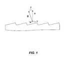
- FIG. 1shows a schematic representation of a vicinal surface with atomic steps or kinks.
- the miscut angle, ⁇is defined as the angle between the surface normal, n, and the primary crystal orientation [uvw], denoted by g.
- Substratesmay be cut from a bulk crystal by those practiced in the art with a specific magnitude of miscut angle. Further, the direction of the miscut vector g may be specified relative to a specific in-plane crystallographic direction [uvw], as denoted by the angle at in FIG. 1 .
- ELOEpitaxial Lateral Overgrowth
- the present inventiondiscloses a method allowing for the growth of planar films of semipolar nitrides, in which a large area of (Al,In,Ga,B)N is parallel to the substrate surface, through the use of intentionally miscut substrates. For example, samples are often grown on 2 inch diameter substrates compared to the few micrometer wide areas previously demonstrated for the growth of semipolar nitrides.
- This inventionalso distinguishes itself from the above mentioned process by allowing the use of a large, typically 2 inch, wafer in which the entire area is a semipolar film. This is in sharp contrast to the above mentioned method in which the semipolar film is only typically 4 mm by 10 mm is size, due to the unavailability of large area GaN crystals.
- the present inventiondiscloses a method for enhancing growth of a device-quality planar semipolar nitride semiconductor film comprising the step of depositing the semipolar nitride semiconductor film on an intentionally miscut substrate.
- the substratemay be intentionally miscut away from a low index crystal orientation and the miscut may comprise a magnitude and direction, wherein the direction and magnitude of miscut may be chosen to affect the epitaxial relationship, crystal symmetry, layer polarity, dislocation density, surface morphology and electrical properties of the semipolar nitride semiconductor film.
- the magnitudemay vary depending on the substrate material, an orientation of the semipolar nitride semiconductor film, a type of deposition, and deposition conditions.
- the magnitude of the miscutmay range from 0.5°-20° or preferably vary between 0.5° and 3°.
- the substratemay be intentionally miscut in a ⁇ 011> direction.
- the growth surface of the semipolar nitride semiconductor filmmay be more than 10 microns wide and substantially parallel to the intentionally miscut substrate's surface.
- the substrate for growth of the semipolar nitride semiconductor filmmay be intentionally miscut in a given crystallographic direction, thereby forming the intentionally miscut substrate and lowering a symmetry of the substrate.
- the symmetrymay match the semipolar nitride semiconductor film's symmetry, resulting in a unique epitaxial relationship, such that the semipolar nitride semiconductor film contains a single crystallographic domain.
- the low symmetry semipolar nitride semiconductor thin filmmay be deposited heteroepitaxially on a higher symmetry substrate.
- the resulting semiconductor thin filmmay have a single polarization direction, resulting in improved electrical, optical, and device properties.
- the intentionally miscut substratemay provide step edges or kinks that serve as preferential nucleation sites for growth of the semipolar nitride semiconductor film.
- the preferential nucleation sitesmay provide for improved layer properties, such as better coalescence of nuclei, reduced defect densities or smoother, more planar interfaces or surfaces, and improved facet stability compared to deposition on non-intentionally miscut substrates.
- the semipolar nitride semiconductor film deposited on the intentionally miscut substratemay have better crystallinity and reduced threading dislocations compared to the semipolar nitride semiconductor film deposited on a non-intentionally miscut substrate. The macroscopic surface roughness and faceting of the semipolar nitride semiconductor film decreases with increasing miscut angle.
- the semipolar nitride semiconductor filmmay be ⁇ 10-11 ⁇ gallium nitride and the intentionally miscut substrate may be ⁇ 100 ⁇ MgAl 2 O 4 spinel substrate miscut in the ⁇ 011> direction.
- the semipolar nitride semiconductor filmmay be ⁇ 11-22 ⁇ GaN and the intentionally miscut substrate may be ⁇ 1-100 ⁇ Al 2 O 3 sapphire substrate miscut in the ⁇ 0001> direction.
- the intentionally miscut substratemay be obtained by cutting a bulk nitride crystal along a semipolar plane and growing the semipolar nitride semiconductor film homoepitaxially on the intentionally miscut substrate.
- the semipolar planemay have a Nitrogen face or a Gallium face.
- the methodmay further comprise (a) intentionally miscutting a substrate, (b) loading the substrate into a reactor, (c) heating the substrate under a flow comprising at least one of nitrogen, hydrogen or ammonia, (d) depositing the semipolar nitride semiconductor film on the heated substrate and (e) cooling the substrate under a nitrogen overpressure.
- the methodmay further comprise depositing a nucleation layer on the heated substrate and depositing the semipolar nitride semiconductor film on the nucleation layer.
- a devicemay be fabricated using the method of the present invention.
- the devicemay be a light emitting diode having a brighter emission than a device fabricated on a non-intentionally miscut substrate.
- the present inventiondescribes a method for enhancing growth of a lower symmetry layer on a higher symmetry substrate comprising intentionally miscutting the higher symmetry substrate to match a symmetry of the lower symmetry layer and depositing the lower symmetry layer heteroepitaxially on the intentionally miscut substrate.
- FIG. 1is a schematic representation of a miscut substrate.
- FIG. 2is a flowchart illustrating the method of the present invention and the process steps used in embodiments of the present invention.
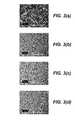
- FIGS. 3( a ), ( b ), ( c ) and ( d )are optical micrographs of semipolar nitride layers deposited on miscut substrates, wherein the substrate in FIG. 3( a ) is not-intentionally miscut, the substrate in FIG. 3( b ) has a miscut angle ⁇ of 0.5 degrees, the substrate in FIG. 3( c ) has a miscut angle ⁇ of 1.5 degrees, and the substrate in FIG. 3( d ) has a miscut angle ⁇ of 3.0 degrees.
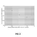
- FIG. 4is a graph illustrating the full width at half-maximum (FWHM) of the (10-11) x-ray rocking curve versus substrate miscut angle ⁇ .
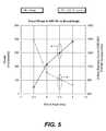
- FIG. 5is a graph illustrating output power (measured in microwatts) and FWHM of the (11-22) x-ray rocking curve (measured in arcseconds) as a function of substrate miscut angle.
- the present inventiondescribes a method for growing semipolar nitride semiconductor films via techniques comprising, but not limited to, MOCVD, HVPE or MBE, on ⁇ 100 ⁇ MgAl 2 O 4 (spinel) substrates miscut in the ⁇ 011> direction and on ⁇ 1-100 ⁇ (m-plane) Al 2 O 3 (sapphire) substrates miscut in the ⁇ 0001> direction.
- MOCVDmetal-vapor deposition
- HVPEHVPE
- MBE⁇ 100 ⁇ MgAl 2 O 4
- m-planem-plane Al 2 O 3
- the use of an intentionally miscut substrateprovides step edges and/or kinks, as shown in FIG. 1 , that serve as preferential nucleation sites for the growth of semipolar nitride layers.
- the application of an intentional miscut in a given crystallographic directionmay lower the symmetry of the substrate used for the growth of semipolar nitride layers relative to the symmetry of the non-intentionally miscut substrate. Symmetry matching of the intentionally miscut substrate to the semipolar nitride layer results in a unique epitaxial relationship, such that the semipolar nitride layer contains a single crystallographic domain.
- the present inventiondiscloses a method of growing high quality semipolar nitride layers using intentionally miscut substrates. Examples of this are ⁇ 10-11 ⁇ GaN films deposited on ⁇ 100 ⁇ MgAl 2 O 4 spinel substrate miscut in the ⁇ 011> direction and ⁇ 11-22 ⁇ GaN films deposited on ⁇ 1-100 ⁇ Al 2 O 3 sapphire substrate miscut in the ⁇ 0001> direction. Due to the lower symmetry of the ⁇ 1-100 ⁇ crystal surface, a miscut towards or away from the ⁇ 1-102 ⁇ sapphire plane may be specified depending on the desired result.
- the magnitude of the miscutvaried from 0.5° to 3.0°, other substrate materials, substrate orientations, miscut angles, and miscut directions may be used without differing from the scope of the present invention, comprising, but not limited to, a range of 0.5°-20°.
- miscut angle and directionmay vary by a small amount relative to the intended miscut angle and direction.
- the miscut magnitudes and directions described hereinrefer to intended values, and small differences are assumed without departing from the scope of the present invention.
- nitride layersoccurs on a vicinal surface.
- the scope of the present inventionincludes all deposition of semipolar nitride layers where the miscut of the substrate is intentionally controlled to result in improved material and/or device properties.
- a general outline of growth parameters for ⁇ 10-11 ⁇ GaNis a pressure between 10 torr and 1000 torr, and a temperature between 400° C. and 1400° C. This variation in pressure and temperature is indicative of the stability of the growth of GaN using a suitable substrate.
- the epitaxial relationships and conditionsshould hold true regardless of the type of reactor. However, the reactor conditions for growing these planes will vary according to individual reactors and growth methods (HVPE, MOCVD, and MBE, for example).
- FIG. 2is a flowchart that illustrates a method for enhancing growth of a device-quality planar semipolar nitride semiconductor thin film comprising growing the semipolar nitride semiconductor film on an intentionally miscut substrate.
- the methodcan also be used for depositing any semipolar nitride film using any suitable substrate.
- Block 200represents the step of intentionally miscutting a substrate.
- Block 202represents the step of loading the intentionally miscut substrate into a deposition or growth chamber, such as an HVPE, MOCVD or MBE reactor, for example.
- a deposition or growth chambersuch as an HVPE, MOCVD or MBE reactor, for example.
- Block 204represents the step of heating the intentionally miscut substrate, typically with nitrogen and/or hydrogen and/or ammonia flowing over the substrate at atmospheric pressure.
- Block 206represents the step of depositing a nucleation or buffer layer on the intentionally miscut substrate.
- Block 208represents the step of depositing a semipolar nitride semiconductor film on the buffer layer, nucleation layer, or directly on the intentionally miscut substrate.
- Block 210represents the step of cooling the substrate, for example under nitrogen or ammonia overpressure.
- Block 212shows how the method may result in the formation of a semipolar (Al, Ga, In, B)N film.
- steps in FIG. 2may be omitted or additional steps may be added as desired.
- the method of FIG. 2may be applied to the MOCVD process for the growth of semipolar GaN thin films on spinel or sapphire substrates according to the preferred embodiments of the present invention.
- a (100) spinel substrateis used with a miscut in the ⁇ 011> direction, as represented in Block 200 .
- the substrateis loaded into an MOCVD reactor, as represented in Block 202 .
- the reactor's heateris turned on and ramped to 1150° C. under conditions to encourage nitridization of the surface of the substrate, as represented in Block 204 .
- nitrogen and/or hydrogen and/or ammoniaflows over the substrate at atmospheric pressure during this step. Once the set point temperature is reached, the ammonia flow is set to 0.1 to 3.0 slpm.
- the reactor set point temperatureis then increased to 1190° C., the reactor pressure is reduced to 76 torr, and 0 to 3 sccm of Trimethylgallium (TMGa) and/or 20 sccm of Trimethylaluminum (TMAl) are introduced into the reactor to initiate the Al x Ga 1 ⁇ x N buffer or nucleation layer growth, as represented in Block 206 .
- TMGaTrimethylgallium
- TMAlTrimethylaluminum
- the Al x Ga 1 ⁇ x N nucleation layerreaches the desired thickness.
- the TMAl flowis shut off and TMGa is increased to 9.5 sccm for approximately 1 to 4 hours of GaN growth, as represented in Block 208 .
- the TMGa flowis interrupted and the reactor is cooled down while flowing ammonia to preserve the GaN film, as represented in Block 210 .
- the growth of ⁇ 11-22 ⁇ GaN, a ⁇ 1-100 ⁇ sapphire substrateis used with a miscut in the ⁇ 0001> direction, as represented in Block 200 .
- the substrateis loaded into an MOCVD reactor, as represented in Block 202 .
- the heateris turned on and ramped to 1150° C., with, generally, nitrogen and/or hydrogen and/or ammonia flowing over the substrate at atmospheric pressure, as represented in Block 204 .
- the reactor set point temperatureis then decreased to 700° C.
- the ammonia flowis set to 0.1 to 3.0 slpm, and 0 to 3 sccm of trimethylgallium (TMGa), and/or 0 to 100 sccm trimethylindium (TMI), and/or 0 to 20 sccm of trimethylaluminum (TMAl) are introduced into the reactor to initiate the Al x In y Ga 1 ⁇ x ⁇ y N buffer layer growth, as represented in Block 206 .
- TMGatrimethylgallium
- TMItrimethylindium
- TMAltrimethylaluminum
- TMAl and/or TMI and/or TMG flowsare shut off, the temperature is increased to 1185° C. and TMGa is increased to 15 sccm for approximately 1 to 4 hours of GaN growth, as represented in Block 208 .
- TMGa flowis interrupted and the reactor is cooled down while flowing ammonia to preserve the GaN film, as represented in Block 210 .
- the scope of the present inventioncovers more than just the particular example cited. This idea is pertinent to all nitrides on any semipolar plane. For example, one could grow ⁇ 10-11 ⁇ AlN, InN, AlGaN, InGaN, or AlInN on a miscut (100) spinel substrate. Another example is that one could grow ⁇ 10-12 ⁇ nitrides, if the proper substrate, such as ⁇ 10-14 ⁇ 4H-SiC, is used. Further, it has been shown the semipolar ⁇ 10-13 ⁇ and ⁇ 11-22 ⁇ semipolar orientations of GaN may be deposited on (10-10) sapphire where the in plane epitaxial relationship of the two orientations differs by a rotation of 90° with respect to substrate. Therefore, it would be expected that improvements in the deposition of these two differing orientations would require the use of differing miscut directions applied to the same substrate.
- Any substrate suitable for the growth of semipolar nitride layersmay be miscut to improve the quality of the deposited nitride layers.
- this inventionrefers specifically to the heteroepitaxial growth of semipolar nitride layers, intentional miscut may also be used to improve the growth of semipolar nitride layers on bulk GaN and AlN substrates.
- semipolar filmscould also be grown homoepitaxially if a GaN or AlN substrate were provided.
- Any bulk growth techniquescould be used, for example, ammonothermal, flux, high pressure, and HVPE.
- Bulk crystalscould be grown in any orientation, (e.g. semipolar, non polar and polar) and subsequently cut and polished on a semipolar plane for subsequent homoepitaxy.
- planar semipolar filmscan be any growth technique that generates a planar semipolar nitride film by using a starting substrate intentionally miscut away from a low index crystal orientation, wherein the miscut may include both a specified magnitude and/or crystallographic direction.
- the magnitude of the miscut angle ⁇may vary depending on the specific substrate material used, the specific semipolar nitride orientation of the deposited layer, the type of deposition technique used, and optimal deposition conditions used.
- the nuclei formed during the MOCVD growth of a GaN layermay be expected to be smaller than the nuclei formed during the HVPE growth of a GaN layer. Therefore, larger miscut angle, which results in a higher density of step edges, may be advantageous for MOCVD growth relative to HVPE growth.
- the direction of the miscutis chosen to lower the symmetry of the substrate such that it matches that of the nitride layer.
- the 4-fold symmetry of (100) spinelis reduced by a miscut in a ⁇ 011> direction.
- this inventionrefers specifically to the growth of semipolar nitride layers, this technique may be used for any material system where a low symmetry layer is deposited heteroepitaxially on a higher symmetry substrate.
- the direction of the miscutis chosen to affect the crystal quality and surface morphology of the semipolar nitride layer.
- the direction and magnitude of miscutmay be chosen to affect any and or all of the crystal properties of the deposited nitride layer including, but not limited to, the epitaxial relationship, crystal symmetry, layer polarity, dislocation density, surface morphology and/or electrical properties.
- the reactor conditionswill vary by reactor type and design.
- the growth described abovedescribes only one set of conditions that has been found to be useful for the growth of semipolar GaN. Other conditions may also be useful for such growth. Specifically, it has also been discovered that these films will grow under a wide parameter space of pressure, temperature, gas flows, and etc., all of which will generate a planar semipolar nitride film.
- nitridizing the substrateimproves surface morphology for some films, and determines the actual plane grown for other films. However, this may or may not be necessary for any particular growth technique.
- the preferred embodimentdescribed the growth of a GaN film on a (100) spinel substrate miscut in a ⁇ 011> direction and comprising an AlGaN nucleation layer.
- the use and composition of the nucleation layeris representative of the deposition technique and system used. However, differing techniques may be used to achieve similar results.
- the structure grown upon the nucleation layermay consist of multiple layers having varying or graded compositions.
- the majority of nitride devicesconsist of heterostructures containing layers of dissimilar (Al,Ga,In,B)N composition.
- Dopants, such as Fe, Si, and Mgare frequently doped into nitride layers. The incorporation of these and other dopants not specifically listed is compatible with the practice of this invention.
- the existing practiceis to grow GaN with the c-plane normal to the surface. This plane has a spontaneous polarization and piezoelectric polarization which are detrimental to device performance.
- the advantage of semipolar over c-plane nitride filmsis the reduction in polarization and the associated increase in internal quantum efficiency for certain devices.
- Nonpolar planescould be used to completely eliminate polarization effects in devices. However, these planes are quite difficult to grow, thus nonpolar nitride devices are not currently in production.
- the advantage of semipolar over nonpolar nitride filmsis the ease of growth. It has been found that semipolar planes have a large parameter space in which they will grow. For example, nonpolar planes will not grow at atmospheric pressure, but semipolar planes have been experimentally demonstrated to grow from 62.5 torr to 760 torr, but probably have an even wider range than that.
- planar semipolar films over ELO sidewallis the large surface area that can be processed into an LED or other device. Another advantage is that the growth surface is parallel to the substrate surface, unlike that of ELO sidewall semipolar planes.
- FIG. 3shows how symmetry matching of the intentionally miscut substrate to the semipolar nitride semiconductor film's symmetry results in a unique epitaxial relationship, such that the semipolar nitride semiconductor thin film contains a single crystallographic domain.
- FIG. 3( a )shows the surface morphology of a (10-11) oriented semipolar GaN film grown on a non-intentionally miscut (100) spinel substrate. The film is comprised of numerous, non-coalesced islands. Additionally, multiple crystal domains, rotated 90 degrees with respect to one another, are visible.
- FIG. 3shows how the preferential nucleation sites on the miscut substrate provide for improved layer properties, such as coalescence of nuclei and smoother, planar interfaces or surfaces compared to deposition on non-intentionally miscut substrates.
- the crystal quality of deposited semiconductor filmsmay be measured by high-resolution x-ray diffraction rocking curve measurements.
- the full width at half-maximum (FWHM) of a suitable x-ray diffraction peakindicates the relative crystal mosaic and defect density of layers being examined.
- the FWHM of the on-axis (10-11) reflectiondecreases with increasing miscut angle, as observed in FIG. 4 . This indicates a reduction in the threading dislocations generated by the heteroepitaxial crystal deposition, for semipolar nitride layers deposited on intentionally miscut substrates.
- the use of an intentionally miscut ⁇ 1-100 ⁇ sapphire substrate for the growth of semipolar ⁇ 11-22 ⁇ nitride layershas been shown to produce better semipolar nitride layers relative to non-intentionally miscut substrates.
- the crystalline quality measured by x-ray diffraction in terms of the FWHM of the ⁇ 11-22 ⁇ rocking curvealso shows that films on intentionally miscut ⁇ 1-100 ⁇ sapphire substrate have better crystallinity than non-intentionally miscut substrates, as shown in FIG. 5 .
- the output power from light-emitting diodes (LEDs) fabricated on the films grown on an intentionally miscut sapphire substratehave shown brighter emission than on non-intentionally miscut substrates, as shown in FIG. 5 .
- Benefits incurred by using semipolar planes for optoelectronic devicesmay be a function of the planes being Gallium (Ga) face or Nitrogen (N) face.
- GaGallium
- NNitrogen
- the exposed surface of the semi polar plane after deposition on the miscut substrateis N face or Ga face, and a device may be deposited on the N face or Ga face.
- the use of intentionally miscut ⁇ 1-100 ⁇ sapphire for the growth of semipolar GaNmay also be used to stabilize surface facets other than ⁇ 11-22 ⁇ . For example, large ⁇ 10-11 ⁇ facets may be stabilized. These facets allow further control of the orientation of the polarization field, increase the device area, and may improve light extraction in optoelectronic devices.
Landscapes
- Chemical & Material Sciences (AREA)
- Engineering & Computer Science (AREA)
- Materials Engineering (AREA)
- Crystallography & Structural Chemistry (AREA)
- Condensed Matter Physics & Semiconductors (AREA)
- Organic Chemistry (AREA)
- Manufacturing & Machinery (AREA)
- Computer Hardware Design (AREA)
- Microelectronics & Electronic Packaging (AREA)
- Power Engineering (AREA)
- General Physics & Mathematics (AREA)
- Metallurgy (AREA)
- Physics & Mathematics (AREA)
- General Chemical & Material Sciences (AREA)
- Chemical Kinetics & Catalysis (AREA)
- Inorganic Chemistry (AREA)
- Crystals, And After-Treatments Of Crystals (AREA)
- Chemical Vapour Deposition (AREA)
- Led Devices (AREA)
Abstract
Description
Claims (26)
Priority Applications (4)
| Application Number | Priority Date | Filing Date | Title |
|---|---|---|---|
| US11/655,573US7691658B2 (en) | 2006-01-20 | 2007-01-19 | Method for improved growth of semipolar (Al,In,Ga,B)N |
| US12/710,181US8110482B2 (en) | 2006-01-20 | 2010-02-22 | Miscut semipolar optoelectronic device |
| US13/311,986US8368179B2 (en) | 2006-01-20 | 2011-12-06 | Miscut semipolar optoelectronic device |
| US13/351,514US20120161287A1 (en) | 2006-01-20 | 2012-01-17 | METHOD FOR ENHANCING GROWTH OF SEMI-POLAR (Al,In,Ga,B)N VIA METALORGANIC CHEMICAL VAPOR DEPOSITION |
Applications Claiming Priority (2)
| Application Number | Priority Date | Filing Date | Title |
|---|---|---|---|
| US76073906P | 2006-01-20 | 2006-01-20 | |
| US11/655,573US7691658B2 (en) | 2006-01-20 | 2007-01-19 | Method for improved growth of semipolar (Al,In,Ga,B)N |
Related Child Applications (1)
| Application Number | Title | Priority Date | Filing Date |
|---|---|---|---|
| US12/710,181ContinuationUS8110482B2 (en) | 2006-01-20 | 2010-02-22 | Miscut semipolar optoelectronic device |
Publications (2)
| Publication Number | Publication Date |
|---|---|
| US20070218703A1 US20070218703A1 (en) | 2007-09-20 |
| US7691658B2true US7691658B2 (en) | 2010-04-06 |
Family
ID=38288327
Family Applications (3)
| Application Number | Title | Priority Date | Filing Date |
|---|---|---|---|
| US11/655,573Active2027-04-21US7691658B2 (en) | 2006-01-20 | 2007-01-19 | Method for improved growth of semipolar (Al,In,Ga,B)N |
| US12/710,181ActiveUS8110482B2 (en) | 2006-01-20 | 2010-02-22 | Miscut semipolar optoelectronic device |
| US13/311,986ActiveUS8368179B2 (en) | 2006-01-20 | 2011-12-06 | Miscut semipolar optoelectronic device |
Family Applications After (2)
| Application Number | Title | Priority Date | Filing Date |
|---|---|---|---|
| US12/710,181ActiveUS8110482B2 (en) | 2006-01-20 | 2010-02-22 | Miscut semipolar optoelectronic device |
| US13/311,986ActiveUS8368179B2 (en) | 2006-01-20 | 2011-12-06 | Miscut semipolar optoelectronic device |
Country Status (6)
| Country | Link |
|---|---|
| US (3) | US7691658B2 (en) |
| EP (1) | EP1982351A4 (en) |
| JP (3) | JP5896442B2 (en) |
| KR (1) | KR101510461B1 (en) |
| TW (1) | TWI490918B (en) |
| WO (1) | WO2007084782A2 (en) |
Cited By (83)
| Publication number | Priority date | Publication date | Assignee | Title |
|---|---|---|---|---|
| US20070093073A1 (en)* | 2005-06-01 | 2007-04-26 | Farrell Robert M Jr | Technique for the growth and fabrication of semipolar (Ga,A1,In,B)N thin films, heterostructures, and devices |
| US20080179607A1 (en)* | 2006-12-11 | 2008-07-31 | The Regents Of The University Of California | Non-polar and semi-polar light emitting devices |
| US20090309127A1 (en)* | 2008-06-13 | 2009-12-17 | Soraa, Inc. | Selective area epitaxy growth method and structure |
| US20090309110A1 (en)* | 2008-06-16 | 2009-12-17 | Soraa, Inc. | Selective area epitaxy growth method and structure for multi-colored devices |
| US20100001300A1 (en)* | 2008-06-25 | 2010-01-07 | Soraa, Inc. | COPACKING CONFIGURATIONS FOR NONPOLAR GaN AND/OR SEMIPOLAR GaN LEDs |
| US20100012948A1 (en)* | 2008-07-16 | 2010-01-21 | Ostendo Technologies, Inc. | Growth of Planar Non-Polar M-Plane and Semi-Polar Gallium Nitride with Hydride Vapor Phase Epitaxy (HVPE) |
| US20100075107A1 (en)* | 2008-05-28 | 2010-03-25 | The Regents Of The University Of California | Hexagonal wurtzite single crystal and hexagonal wurtzite single crystal substrate |
| US20100133663A1 (en)* | 2005-03-10 | 2010-06-03 | The Regents Of The University Of California | Technique for the growth of planar semi-polar gallium nitride |
| US20100302464A1 (en)* | 2009-05-29 | 2010-12-02 | Soraa, Inc. | Laser Based Display Method and System |
| US20110056429A1 (en)* | 2009-08-21 | 2011-03-10 | Soraa, Inc. | Rapid Growth Method and Structures for Gallium and Nitrogen Containing Ultra-Thin Epitaxial Structures for Devices |
| US20110064100A1 (en)* | 2009-09-17 | 2011-03-17 | Kaai, Inc. | Growth Structures and Method for Forming Laser Diodes on or Off Cut Gallium and Nitrogen Containing Substrates |
| US20110108954A1 (en)* | 2009-11-06 | 2011-05-12 | Ostendo Technologies, Inc. | Growth of Planar Non-Polar M-Plane Gallium Nitride With Hydride Vapor Phase Epitaxy (HVPE) |
| US20110180781A1 (en)* | 2008-06-05 | 2011-07-28 | Soraa, Inc | Highly Polarized White Light Source By Combining Blue LED on Semipolar or Nonpolar GaN with Yellow LED on Semipolar or Nonpolar GaN |
| US20110182056A1 (en)* | 2010-06-23 | 2011-07-28 | Soraa, Inc. | Quantum Dot Wavelength Conversion for Optical Devices Using Nonpolar or Semipolar Gallium Containing Materials |
| US8259769B1 (en) | 2008-07-14 | 2012-09-04 | Soraa, Inc. | Integrated total internal reflectors for high-gain laser diodes with high quality cleaved facets on nonpolar/semipolar GaN substrates |
| US8451876B1 (en) | 2010-05-17 | 2013-05-28 | Soraa, Inc. | Method and system for providing bidirectional light sources with broad spectrum |
| US8494017B2 (en) | 2008-08-04 | 2013-07-23 | Soraa, Inc. | Solid state laser device using a selected crystal orientation in non-polar or semi-polar GaN containing materials and methods |
| US8509275B1 (en) | 2009-05-29 | 2013-08-13 | Soraa, Inc. | Gallium nitride based laser dazzling device and method |
| US8524578B1 (en) | 2009-05-29 | 2013-09-03 | Soraa, Inc. | Method and surface morphology of non-polar gallium nitride containing substrates |
| US8558265B2 (en) | 2008-08-04 | 2013-10-15 | Soraa, Inc. | White light devices using non-polar or semipolar gallium containing materials and phosphors |
| US8709921B2 (en) | 2010-11-15 | 2014-04-29 | Applied Materials, Inc. | Method for forming a semiconductor device using selective epitaxy of group III-nitride |
| US8728842B2 (en) | 2008-07-14 | 2014-05-20 | Soraa Laser Diode, Inc. | Self-aligned multi-dielectric-layer lift off process for laser diode stripes |
| US8750342B1 (en) | 2011-09-09 | 2014-06-10 | Soraa Laser Diode, Inc. | Laser diodes with scribe structures |
| US8805134B1 (en) | 2012-02-17 | 2014-08-12 | Soraa Laser Diode, Inc. | Methods and apparatus for photonic integration in non-polar and semi-polar oriented wave-guided optical devices |
| US8816319B1 (en) | 2010-11-05 | 2014-08-26 | Soraa Laser Diode, Inc. | Method of strain engineering and related optical device using a gallium and nitrogen containing active region |
| US8837545B2 (en) | 2009-04-13 | 2014-09-16 | Soraa Laser Diode, Inc. | Optical device structure using GaN substrates and growth structures for laser applications |
| US8905588B2 (en) | 2010-02-03 | 2014-12-09 | Sorra, Inc. | System and method for providing color light sources in proximity to predetermined wavelength conversion structures |
| US20150008563A1 (en)* | 2006-11-17 | 2015-01-08 | Sumitomo Electric Industries, Ltd. | Composite of III-Nitride Crystal on Laterally Stacked Substrates |
| US8956896B2 (en) | 2006-12-11 | 2015-02-17 | The Regents Of The University Of California | Metalorganic chemical vapor deposition (MOCVD) growth of high performance non-polar III-nitride optical devices |
| US8971368B1 (en) | 2012-08-16 | 2015-03-03 | Soraa Laser Diode, Inc. | Laser devices having a gallium and nitrogen containing semipolar surface orientation |
| US8971370B1 (en) | 2011-10-13 | 2015-03-03 | Soraa Laser Diode, Inc. | Laser devices using a semipolar plane |
| US9020003B1 (en) | 2012-03-14 | 2015-04-28 | Soraa Laser Diode, Inc. | Group III-nitride laser diode grown on a semi-polar orientation of gallium and nitrogen containing substrates |
| US9025635B2 (en) | 2011-01-24 | 2015-05-05 | Soraa Laser Diode, Inc. | Laser package having multiple emitters configured on a support member |
| US9048170B2 (en) | 2010-11-09 | 2015-06-02 | Soraa Laser Diode, Inc. | Method of fabricating optical devices using laser treatment |
| US9071039B2 (en) | 2009-04-13 | 2015-06-30 | Soraa Laser Diode, Inc. | Optical device structure using GaN substrates for laser applications |
| US9093820B1 (en) | 2011-01-25 | 2015-07-28 | Soraa Laser Diode, Inc. | Method and structure for laser devices using optical blocking regions |
| US9099843B1 (en) | 2012-07-19 | 2015-08-04 | Soraa Laser Diode, Inc. | High operating temperature laser diodes |
| US9166372B1 (en) | 2013-06-28 | 2015-10-20 | Soraa Laser Diode, Inc. | Gallium nitride containing laser device configured on a patterned substrate |
| US9209596B1 (en) | 2014-02-07 | 2015-12-08 | Soraa Laser Diode, Inc. | Manufacturing a laser diode device from a plurality of gallium and nitrogen containing substrates |
| US9236530B2 (en) | 2011-04-01 | 2016-01-12 | Soraa, Inc. | Miscut bulk substrates |
| US9246311B1 (en) | 2014-11-06 | 2016-01-26 | Soraa Laser Diode, Inc. | Method of manufacture for an ultraviolet laser diode |
| US9250044B1 (en) | 2009-05-29 | 2016-02-02 | Soraa Laser Diode, Inc. | Gallium and nitrogen containing laser diode dazzling devices and methods of use |
| US9287684B2 (en) | 2011-04-04 | 2016-03-15 | Soraa Laser Diode, Inc. | Laser package having multiple emitters with color wheel |
| US9318875B1 (en) | 2011-01-24 | 2016-04-19 | Soraa Laser Diode, Inc. | Color converting element for laser diode |
| US9343871B1 (en) | 2012-04-05 | 2016-05-17 | Soraa Laser Diode, Inc. | Facet on a gallium and nitrogen containing laser diode |
| US9362715B2 (en) | 2014-02-10 | 2016-06-07 | Soraa Laser Diode, Inc | Method for manufacturing gallium and nitrogen bearing laser devices with improved usage of substrate material |
| US9368939B2 (en) | 2013-10-18 | 2016-06-14 | Soraa Laser Diode, Inc. | Manufacturable laser diode formed on C-plane gallium and nitrogen material |
| US9379525B2 (en) | 2014-02-10 | 2016-06-28 | Soraa Laser Diode, Inc. | Manufacturable laser diode |
| US9520695B2 (en) | 2013-10-18 | 2016-12-13 | Soraa Laser Diode, Inc. | Gallium and nitrogen containing laser device having confinement region |
| US9520697B2 (en) | 2014-02-10 | 2016-12-13 | Soraa Laser Diode, Inc. | Manufacturable multi-emitter laser diode |
| US9531164B2 (en) | 2009-04-13 | 2016-12-27 | Soraa Laser Diode, Inc. | Optical device structure using GaN substrates for laser applications |
| US9564736B1 (en) | 2014-06-26 | 2017-02-07 | Soraa Laser Diode, Inc. | Epitaxial growth of p-type cladding regions using nitrogen gas for a gallium and nitrogen containing laser diode |
| US9583340B2 (en) | 2013-11-05 | 2017-02-28 | Samsung Electronics Co., Ltd. | Semipolar nitride semiconductor structure and method of manufacturing the same |
| US9595813B2 (en) | 2011-01-24 | 2017-03-14 | Soraa Laser Diode, Inc. | Laser package having multiple emitters configured on a substrate member |
| US9646827B1 (en) | 2011-08-23 | 2017-05-09 | Soraa, Inc. | Method for smoothing surface of a substrate containing gallium and nitrogen |
| US9653642B1 (en) | 2014-12-23 | 2017-05-16 | Soraa Laser Diode, Inc. | Manufacturable RGB display based on thin film gallium and nitrogen containing light emitting diodes |
| US9666677B1 (en) | 2014-12-23 | 2017-05-30 | Soraa Laser Diode, Inc. | Manufacturable thin film gallium and nitrogen containing devices |
| US20170200806A1 (en)* | 2014-10-03 | 2017-07-13 | Ngk Insulators, Ltd. | Epitaxial Substrate for Semiconductor Device and Method for Manufacturing Same |
| US9787963B2 (en) | 2015-10-08 | 2017-10-10 | Soraa Laser Diode, Inc. | Laser lighting having selective resolution |
| US9800016B1 (en) | 2012-04-05 | 2017-10-24 | Soraa Laser Diode, Inc. | Facet on a gallium and nitrogen containing laser diode |
| US9800017B1 (en) | 2009-05-29 | 2017-10-24 | Soraa Laser Diode, Inc. | Laser device and method for a vehicle |
| US9829780B2 (en) | 2009-05-29 | 2017-11-28 | Soraa Laser Diode, Inc. | Laser light source for a vehicle |
| US9871350B2 (en) | 2014-02-10 | 2018-01-16 | Soraa Laser Diode, Inc. | Manufacturable RGB laser diode source |
| US9927611B2 (en) | 2010-03-29 | 2018-03-27 | Soraa Laser Diode, Inc. | Wearable laser based display method and system |
| US10108079B2 (en) | 2009-05-29 | 2018-10-23 | Soraa Laser Diode, Inc. | Laser light source for a vehicle |
| US10147850B1 (en) | 2010-02-03 | 2018-12-04 | Soraa, Inc. | System and method for providing color light sources in proximity to predetermined wavelength conversion structures |
| US10222474B1 (en) | 2017-12-13 | 2019-03-05 | Soraa Laser Diode, Inc. | Lidar systems including a gallium and nitrogen containing laser light source |
| US10551728B1 (en) | 2018-04-10 | 2020-02-04 | Soraa Laser Diode, Inc. | Structured phosphors for dynamic lighting |
| US10559939B1 (en) | 2012-04-05 | 2020-02-11 | Soraa Laser Diode, Inc. | Facet on a gallium and nitrogen containing laser diode |
| US10771155B2 (en) | 2017-09-28 | 2020-09-08 | Soraa Laser Diode, Inc. | Intelligent visible light with a gallium and nitrogen containing laser source |
| US10879673B2 (en) | 2015-08-19 | 2020-12-29 | Soraa Laser Diode, Inc. | Integrated white light source using a laser diode and a phosphor in a surface mount device package |
| US10903623B2 (en) | 2019-05-14 | 2021-01-26 | Soraa Laser Diode, Inc. | Method and structure for manufacturable large area gallium and nitrogen containing substrate |
| US10938182B2 (en) | 2015-08-19 | 2021-03-02 | Soraa Laser Diode, Inc. | Specialized integrated light source using a laser diode |
| US11228158B2 (en) | 2019-05-14 | 2022-01-18 | Kyocera Sld Laser, Inc. | Manufacturable laser diodes on a large area gallium and nitrogen containing substrate |
| US11239637B2 (en) | 2018-12-21 | 2022-02-01 | Kyocera Sld Laser, Inc. | Fiber delivered laser induced white light system |
| US11421843B2 (en) | 2018-12-21 | 2022-08-23 | Kyocera Sld Laser, Inc. | Fiber-delivered laser-induced dynamic light system |
| US11437774B2 (en) | 2015-08-19 | 2022-09-06 | Kyocera Sld Laser, Inc. | High-luminous flux laser-based white light source |
| US11437775B2 (en) | 2015-08-19 | 2022-09-06 | Kyocera Sld Laser, Inc. | Integrated light source using a laser diode |
| US11884202B2 (en) | 2019-01-18 | 2024-01-30 | Kyocera Sld Laser, Inc. | Laser-based fiber-coupled white light system |
| US12000552B2 (en) | 2019-01-18 | 2024-06-04 | Kyocera Sld Laser, Inc. | Laser-based fiber-coupled white light system for a vehicle |
| US12126143B2 (en) | 2014-11-06 | 2024-10-22 | Kyocera Sld Laser, Inc. | Method of manufacture for an ultraviolet emitting optoelectronic device |
| US12152742B2 (en) | 2019-01-18 | 2024-11-26 | Kyocera Sld Laser, Inc. | Laser-based light guide-coupled wide-spectrum light system |
| US12191626B1 (en) | 2020-07-31 | 2025-01-07 | Kyocera Sld Laser, Inc. | Vertically emitting laser devices and chip-scale-package laser devices and laser-based, white light emitting devices |
Families Citing this family (73)
| Publication number | Priority date | Publication date | Assignee | Title |
|---|---|---|---|---|
| US7723154B1 (en) | 2005-10-19 | 2010-05-25 | North Carolina State University | Methods of forming zinc oxide based II-VI compound semiconductor layers with shallow acceptor conductivities |
| EP1984545A4 (en)* | 2006-02-17 | 2013-05-15 | Univ California | PROCESS FOR THE PRODUCTION OF N-TYPE SEMIPOLAR OPTOELECTRONIC DEVICES (AL, IN, GA, B) |
| US8728234B2 (en) | 2008-06-04 | 2014-05-20 | Sixpoint Materials, Inc. | Methods for producing improved crystallinity group III-nitride crystals from initial group III-nitride seed by ammonothermal growth |
| US20100095882A1 (en)* | 2008-10-16 | 2010-04-22 | Tadao Hashimoto | Reactor design for growing group iii nitride crystals and method of growing group iii nitride crystals |
| CA2669228C (en)* | 2006-11-15 | 2014-12-16 | The Regents Of The University Of California | Method for heteroepitaxial growth of high-quality n-face gan, inn, and ain and their alloys by metal organic chemical vapor deposition |
| US8193020B2 (en)* | 2006-11-15 | 2012-06-05 | The Regents Of The University Of California | Method for heteroepitaxial growth of high-quality N-face GaN, InN, and AlN and their alloys by metal organic chemical vapor deposition |
| EP2171748A1 (en)* | 2007-07-26 | 2010-04-07 | S.O.I.Tec Silicon on Insulator Technologies | Epitaxial methods and templates grown by the methods |
| WO2009021201A1 (en) | 2007-08-08 | 2009-02-12 | The Regents Of The University Of California | Planar nonpolar m-plane group iii-nitride films grown on miscut substrates |
| WO2009039408A1 (en)* | 2007-09-19 | 2009-03-26 | The Regents Of The University Of California | Method for increasing the area of non-polar and semi-polar nitride substrates |
| JP5262545B2 (en)* | 2007-10-29 | 2013-08-14 | 日立電線株式会社 | Nitride semiconductor free-standing substrate and device using the same |
| US7790230B2 (en)* | 2008-01-30 | 2010-09-07 | The United States Of America As Represented By The Secretary Of The Navy | Metal chloride seeded growth of electronic and optical materials |
| JP2011511462A (en)* | 2008-02-01 | 2011-04-07 | ザ リージェンツ オブ ザ ユニバーシティ オブ カリフォルニア | Enhanced polarization of nitride light-emitting diodes by off-axis wafer cutting |
| JP5241855B2 (en)* | 2008-02-25 | 2013-07-17 | シックスポイント マテリアルズ, インコーポレイテッド | Method for producing group III nitride wafer and group III nitride wafer |
| JP4539752B2 (en)* | 2008-04-09 | 2010-09-08 | 住友電気工業株式会社 | Method for forming quantum well structure and method for manufacturing semiconductor light emitting device |
| WO2009143229A1 (en)* | 2008-05-21 | 2009-11-26 | Lumenz, Inc. | Semiconductor device having rough sidewall |
| US9048169B2 (en)* | 2008-05-23 | 2015-06-02 | Soitec | Formation of substantially pit free indium gallium nitride |
| KR101810613B1 (en)* | 2008-05-28 | 2017-12-20 | 더 리전츠 오브 더 유니버시티 오브 캘리포니아 | Hexagonal wurtzite single crystal |
| EP2291551B1 (en) | 2008-06-04 | 2018-04-25 | SixPoint Materials, Inc. | High-pressure vessel for growing group iii nitride crystals and method of growing group iii nitride crystals using high-pressure vessel and group iii nitride crystal |
| US8871024B2 (en) | 2008-06-05 | 2014-10-28 | Soraa, Inc. | High pressure apparatus and method for nitride crystal growth |
| US9157167B1 (en) | 2008-06-05 | 2015-10-13 | Soraa, Inc. | High pressure apparatus and method for nitride crystal growth |
| US8097081B2 (en) | 2008-06-05 | 2012-01-17 | Soraa, Inc. | High pressure apparatus and method for nitride crystal growth |
| WO2009151642A1 (en) | 2008-06-12 | 2009-12-17 | Sixpoint Materials, Inc. | Method for testing group-iii nitride wafers and group iii-nitride wafers with test data |
| US9404197B2 (en) | 2008-07-07 | 2016-08-02 | Soraa, Inc. | Large area, low-defect gallium-containing nitride crystals, method of making, and method of use |
| JP2010042980A (en)* | 2008-07-17 | 2010-02-25 | Sumitomo Electric Ind Ltd | Method for producing group iii nitride crystal and group iii nitride crystal |
| JP4475358B1 (en)* | 2008-08-04 | 2010-06-09 | 住友電気工業株式会社 | GaN-based semiconductor optical device, method for manufacturing GaN-based semiconductor optical device, and epitaxial wafer |
| US8979999B2 (en) | 2008-08-07 | 2015-03-17 | Soraa, Inc. | Process for large-scale ammonothermal manufacturing of gallium nitride boules |
| US10036099B2 (en) | 2008-08-07 | 2018-07-31 | Slt Technologies, Inc. | Process for large-scale ammonothermal manufacturing of gallium nitride boules |
| JP4917585B2 (en)* | 2008-08-26 | 2012-04-18 | 住友電気工業株式会社 | Method for manufacturing nitride-based semiconductor optical device and method for manufacturing epitaxial wafer |
| US8431419B2 (en)* | 2008-08-28 | 2013-04-30 | Soitec | UV absorption based monitor and control of chloride gas stream |
| US7976630B2 (en) | 2008-09-11 | 2011-07-12 | Soraa, Inc. | Large-area seed for ammonothermal growth of bulk gallium nitride and method of manufacture |
| US8852341B2 (en)* | 2008-11-24 | 2014-10-07 | Sixpoint Materials, Inc. | Methods for producing GaN nutrient for ammonothermal growth |
| US9543392B1 (en) | 2008-12-12 | 2017-01-10 | Soraa, Inc. | Transparent group III metal nitride and method of manufacture |
| US8878230B2 (en) | 2010-03-11 | 2014-11-04 | Soraa, Inc. | Semi-insulating group III metal nitride and method of manufacture |
| US8987156B2 (en) | 2008-12-12 | 2015-03-24 | Soraa, Inc. | Polycrystalline group III metal nitride with getter and method of making |
| US20100147210A1 (en)* | 2008-12-12 | 2010-06-17 | Soraa, Inc. | high pressure apparatus and method for nitride crystal growth |
| US9589792B2 (en) | 2012-11-26 | 2017-03-07 | Soraa, Inc. | High quality group-III metal nitride crystals, methods of making, and methods of use |
| USRE47114E1 (en) | 2008-12-12 | 2018-11-06 | Slt Technologies, Inc. | Polycrystalline group III metal nitride with getter and method of making |
| WO2010101946A1 (en)* | 2009-03-02 | 2010-09-10 | The Regents Of The University Of California | DEVICES GROWN ON NONPOLAR OR SEMIPOLAR (Ga,Al,In,B)N SUBSTRATES |
| US8252662B1 (en) | 2009-03-28 | 2012-08-28 | Soraa, Inc. | Method and structure for manufacture of light emitting diode devices using bulk GaN |
| TW201039381A (en)* | 2009-04-29 | 2010-11-01 | Applied Materials Inc | Method of forming in-situ pre-GaN deposition layer in HVPE |
| WO2010129718A2 (en) | 2009-05-05 | 2010-11-11 | Sixpoint Materials, Inc. | Growth reactor for gallium-nitride crystals using ammonia and hydrogen chloride |
| US20100309943A1 (en)* | 2009-06-05 | 2010-12-09 | The Regents Of The University Of California | LONG WAVELENGTH NONPOLAR AND SEMIPOLAR (Al,Ga,In)N BASED LASER DIODES |
| JP5446622B2 (en)* | 2009-06-29 | 2014-03-19 | 住友電気工業株式会社 | Group III nitride crystal and method for producing the same |
| JP5888317B2 (en)* | 2009-06-29 | 2016-03-22 | 住友電気工業株式会社 | Group III nitride crystals |
| JP2011042542A (en)* | 2009-08-24 | 2011-03-03 | Furukawa Co Ltd | Method for producing group iii nitride substrate, and group iii nitride substrate |
| US8436362B2 (en) | 2009-08-24 | 2013-05-07 | Micron Technology, Inc. | Solid state lighting devices with selected thermal expansion and/or surface characteristics, and associated methods |
| US9175418B2 (en) | 2009-10-09 | 2015-11-03 | Soraa, Inc. | Method for synthesis of high quality large area bulk gallium based crystals |
| JP2011103400A (en)* | 2009-11-11 | 2011-05-26 | Sumitomo Electric Ind Ltd | Compound semiconductor element |
| WO2011109754A1 (en) | 2010-03-04 | 2011-09-09 | The Regents Of The University Of California | Semi-polar iii-nitride optoelectronic devices on m-plane substrates with miscuts less than +/-15 degrees in the c-direction |
| US8445890B2 (en)* | 2010-03-09 | 2013-05-21 | Micron Technology, Inc. | Solid state lighting devices grown on semi-polar facets and associated methods of manufacturing |
| US7829376B1 (en) | 2010-04-07 | 2010-11-09 | Lumenz, Inc. | Methods of forming zinc oxide based II-VI compound semiconductor layers with shallow acceptor conductivities |
| US9564320B2 (en) | 2010-06-18 | 2017-02-07 | Soraa, Inc. | Large area nitride crystal and method for making it |
| GB2482188A (en)* | 2010-07-23 | 2012-01-25 | Univ Leiden | Two dimensional film formation |
| US8729559B2 (en)* | 2010-10-13 | 2014-05-20 | Soraa, Inc. | Method of making bulk InGaN substrates and devices thereon |
| US9694158B2 (en) | 2011-10-21 | 2017-07-04 | Ahmad Mohamad Slim | Torque for incrementally advancing a catheter during right heart catheterization |
| US10029955B1 (en) | 2011-10-24 | 2018-07-24 | Slt Technologies, Inc. | Capsule for high pressure, high temperature processing of materials and methods of use |
| US10145026B2 (en) | 2012-06-04 | 2018-12-04 | Slt Technologies, Inc. | Process for large-scale ammonothermal manufacturing of semipolar gallium nitride boules |
| US9275912B1 (en) | 2012-08-30 | 2016-03-01 | Soraa, Inc. | Method for quantification of extended defects in gallium-containing nitride crystals |
| US9299555B1 (en) | 2012-09-28 | 2016-03-29 | Soraa, Inc. | Ultrapure mineralizers and methods for nitride crystal growth |
| US20140183579A1 (en)* | 2013-01-02 | 2014-07-03 | Japan Science And Technology Agency | Miscut semipolar optoelectronic device |
| US9650723B1 (en) | 2013-04-11 | 2017-05-16 | Soraa, Inc. | Large area seed crystal for ammonothermal crystal growth and method of making |
| KR102140789B1 (en)* | 2014-02-17 | 2020-08-03 | 삼성전자주식회사 | Evaluating apparatus for quality of crystal, and Apparatus and method for manufacturing semiconductor light emitting device which include the same |
| JP6573154B2 (en) | 2014-06-05 | 2019-09-11 | パナソニックIpマネジメント株式会社 | Nitride semiconductor structure, electronic device with nitride semiconductor structure, light emitting device with nitride semiconductor structure, and method for manufacturing nitride semiconductor structure |
| KR102299362B1 (en) | 2014-08-21 | 2021-09-08 | 삼성전자주식회사 | Green light emitting device including quaternary quantum well on a vicinal c-plane |
| KR102356457B1 (en) | 2015-05-29 | 2022-01-27 | 삼성전자주식회사 | Semiconductor laser diode and fabricating the same |
| US10174438B2 (en) | 2017-03-30 | 2019-01-08 | Slt Technologies, Inc. | Apparatus for high pressure reaction |
| CN107086173B (en)* | 2017-04-01 | 2019-10-25 | 天津三安光电有限公司 | Nitride bottom layer and preparation method thereof |
| US11466384B2 (en) | 2019-01-08 | 2022-10-11 | Slt Technologies, Inc. | Method of forming a high quality group-III metal nitride boule or wafer using a patterned substrate |
| WO2021162727A1 (en) | 2020-02-11 | 2021-08-19 | SLT Technologies, Inc | Improved group iii nitride substrate, method of making, and method of use |
| US12091771B2 (en) | 2020-02-11 | 2024-09-17 | Slt Technologies, Inc. | Large area group III nitride crystals and substrates, methods of making, and methods of use |
| US11721549B2 (en) | 2020-02-11 | 2023-08-08 | Slt Technologies, Inc. | Large area group III nitride crystals and substrates, methods of making, and methods of use |
| CN111948235B (en)* | 2020-08-07 | 2022-09-20 | 广西大学 | Method for measuring semipolar plane III group nitride film defect density and application thereof |
| CN115117165A (en)* | 2021-03-19 | 2022-09-27 | 苏州能讯高能半导体有限公司 | Epitaxial structure, preparation method of epitaxial structure, and semiconductor device |
Citations (38)
| Publication number | Priority date | Publication date | Assignee | Title |
|---|---|---|---|---|
| US4855249A (en) | 1985-11-18 | 1989-08-08 | Nagoya University | Process for growing III-V compound semiconductors on sapphire using a buffer layer |
| EP0383215A2 (en) | 1989-02-13 | 1990-08-22 | Nippon Telegraph And Telephone Corporation | Epitaxial-growth structure for a semiconductor light-emitting device, and semiconductor light-emitting device using the same |
| US5716450A (en) | 1994-04-08 | 1998-02-10 | Japan Energy Corporation | Growing method of gallium nitride related compound semiconductor crystal and gallium nitride related compound semiconductor device |
| US5741724A (en) | 1996-12-27 | 1998-04-21 | Motorola | Method of growing gallium nitride on a spinel substrate |
| US6039803A (en) | 1996-06-28 | 2000-03-21 | Massachusetts Institute Of Technology | Utilization of miscut substrates to improve relaxed graded silicon-germanium and germanium layers on silicon |
| US6064082A (en) | 1997-05-30 | 2000-05-16 | Sony Corporation | Heterojunction field effect transistor |
| US6133593A (en) | 1999-07-23 | 2000-10-17 | The United States Of America As Represented By The Secretary Of The Navy | Channel design to reduce impact ionization in heterostructure field-effect transistors |
| US6153010A (en) | 1997-04-11 | 2000-11-28 | Nichia Chemical Industries Ltd. | Method of growing nitride semiconductors, nitride semiconductor substrate and nitride semiconductor device |
| US6218280B1 (en) | 1998-06-18 | 2001-04-17 | University Of Florida | Method and apparatus for producing group-III nitrides |
| US20010009134A1 (en)* | 1998-10-15 | 2001-07-26 | Lg Electronics Inc. | GaN system compound semiconductor and method for growing crystal thereof |
| US20010015437A1 (en) | 2000-01-25 | 2001-08-23 | Hirotatsu Ishii | GaN field-effect transistor, inverter device, and production processes therefor |
| US20010020700A1 (en) | 2000-01-13 | 2001-09-13 | Kaoru Inoue | Semiconductor device |
| US6316785B1 (en) | 1998-10-15 | 2001-11-13 | Kabushiki Kaisha Toshiba | Nitride-compound semiconductor device |
| JP2001342100A (en) | 2000-03-29 | 2001-12-11 | Toshiba Corp | Method for manufacturing substrate for epitaxial growth and method for manufacturing semiconductor device using substrate for epitaxial growth |
| US20020069817A1 (en) | 2000-07-21 | 2002-06-13 | Mishra Umesh Kumar | Method to reduce the dislocation density in group III-nitride films |
| US6440823B1 (en) | 1994-01-27 | 2002-08-27 | Advanced Technology Materials, Inc. | Low defect density (Ga, Al, In)N and HVPE process for making same |
| US20020144645A1 (en) | 1998-11-24 | 2002-10-10 | Kim Andrew Y. | Method of producing device quality (Al)InGaP alloys on lattice-mismatched substrates |
| US20030006407A1 (en) | 1996-10-16 | 2003-01-09 | Taylor Geoff W. | Apparatus and a method of fabricating inversion channel devices with precision gate doping for a monolithic integrated circuit |
| US6599362B2 (en) | 2001-01-03 | 2003-07-29 | Sandia Corporation | Cantilever epitaxial process |
| US6608328B2 (en) | 2001-02-05 | 2003-08-19 | Uni Light Technology Inc. | Semiconductor light emitting diode on a misoriented substrate |
| US6624452B2 (en) | 2000-07-28 | 2003-09-23 | The Regents Of The University Of California | Gallium nitride-based HFET and a method for fabricating a gallium nitride-based HFET |
| US20030198837A1 (en) | 2002-04-15 | 2003-10-23 | Craven Michael D. | Non-polar a-plane gallium nitride thin films grown by metalorganic chemical vapor deposition |
| EP1385196A2 (en) | 2002-07-19 | 2004-01-28 | Toyoda Gosei Co., Ltd. | Method of producing a Group III nitride semiconductor crystal |
| US20040251471A1 (en) | 2001-10-26 | 2004-12-16 | Robert Dwilinski | Light emitting element structure using nitride bulk single crystal layer |
| US20040261692A1 (en) | 2001-10-26 | 2004-12-30 | Robert Dwilinski | Substrate for epitaxy |
| US6847057B1 (en) | 2003-08-01 | 2005-01-25 | Lumileds Lighting U.S., Llc | Semiconductor light emitting devices |
| US20050142391A1 (en) | 2001-07-06 | 2005-06-30 | Technologies And Devices International, Inc. | Method and apparatus for fabricating crack-free Group III nitride semiconductor materials |
| US20050161697A1 (en) | 2001-09-19 | 2005-07-28 | Sumitomo Electric Industries, Ltd. | AlxInyGa1-x-yN mixture crystal substrate, method of growing same and method of producing same |
| US20050214992A1 (en) | 2002-12-16 | 2005-09-29 | The Regents Of The University Of California | Fabrication of nonpolar indium gallium nitride thin films, heterostructures and devices by metalorganic chemical vapor deposition |
| US20050245095A1 (en) | 2002-04-15 | 2005-11-03 | The Regents Of The University Of California | Growth of planar reduced dislocation density m-plane gallium nitride by hydride vapor phase epitaxy |
| US20050258451A1 (en) | 2004-05-20 | 2005-11-24 | Saxler Adam W | Methods of fabricating nitride-based transistors having regrown ohmic contact regions and nitride-based transistors having regrown ohmic contact regions |
| US20060008941A1 (en) | 2002-12-16 | 2006-01-12 | Basf Aktiengesellschaft | Growth of planar, non-polar a-plane gallium nitride by hydride vapor phase epitaxy |
| US20060138431A1 (en) | 2002-05-17 | 2006-06-29 | Robert Dwilinski | Light emitting device structure having nitride bulk single crystal layer |
| US20060270076A1 (en) | 2005-05-31 | 2006-11-30 | The Regents Of The University Of California | Defect reduction of non-polar and semi-polar III-nitrides with sidewall lateral epitaxial overgrowth (SLEO) |
| US20070015345A1 (en) | 2005-07-13 | 2007-01-18 | Baker Troy J | Lateral growth method for defect reduction of semipolar nitride films |
| US20070093073A1 (en) | 2005-06-01 | 2007-04-26 | Farrell Robert M Jr | Technique for the growth and fabrication of semipolar (Ga,A1,In,B)N thin films, heterostructures, and devices |
| US20070111531A1 (en) | 2005-03-10 | 2007-05-17 | The Regents Of The University Of California | Technique for the growth of planar semi-polar gallium nitride |
| US7220658B2 (en) | 2002-12-16 | 2007-05-22 | The Regents Of The University Of California | Growth of reduced dislocation density non-polar gallium nitride by hydride vapor phase epitaxy |
Family Cites Families (13)
| Publication number | Priority date | Publication date | Assignee | Title |
|---|---|---|---|---|
| US6530922B2 (en)* | 1993-12-15 | 2003-03-11 | Sherwood Services Ag | Cluster ablation electrode system |
| JP3119200B2 (en)* | 1997-06-09 | 2000-12-18 | 日本電気株式会社 | Crystal growth method for nitride-based compound semiconductor and gallium nitride-based light emitting device |
| JP2000216497A (en)* | 1999-01-22 | 2000-08-04 | Sanyo Electric Co Ltd | Semiconductor element and its manufacture |
| US6586819B2 (en) | 2000-08-14 | 2003-07-01 | Nippon Telegraph And Telephone Corporation | Sapphire substrate, semiconductor device, electronic component, and crystal growing method |
| US6635904B2 (en)* | 2001-03-29 | 2003-10-21 | Lumileds Lighting U.S., Llc | Indium gallium nitride smoothing structures for III-nitride devices |
| US20030022525A1 (en)* | 2001-07-16 | 2003-01-30 | Motorola, Inc. | Semiconductor structure and device including a monocrystalline layer formed overlying a compliant substrate and a method of forming the same |
| JP3768943B2 (en)* | 2001-09-28 | 2006-04-19 | 日本碍子株式会社 | Group III nitride epitaxial substrate, group III nitride device epitaxial substrate, and group III nitride device |
| JP4031628B2 (en)* | 2001-10-03 | 2008-01-09 | 松下電器産業株式会社 | Semiconductor multilayer crystal, light-emitting element using the same, and method for growing the semiconductor multilayer crystal |
| US7364619B2 (en)* | 2002-06-26 | 2008-04-29 | Ammono. Sp. Zo.O. | Process for obtaining of bulk monocrystalline gallium-containing nitride |
| JP4560310B2 (en)* | 2004-03-03 | 2010-10-13 | 株式会社リコー | Method for manufacturing substrate of group III nitride crystal |
| JP2005277254A (en)* | 2004-03-26 | 2005-10-06 | Shikusuon:Kk | Substrate and manufacturing method thereof |
| JP5194334B2 (en)* | 2004-05-18 | 2013-05-08 | 住友電気工業株式会社 | Method for manufacturing group III nitride semiconductor device |
| JP4432827B2 (en)* | 2005-04-26 | 2010-03-17 | 住友電気工業株式会社 | Group III nitride semiconductor device and epitaxial substrate |
- 2007
- 2007-01-19TWTW096102148Apatent/TWI490918B/ennot_activeIP Right Cessation
- 2007-01-19JPJP2008551465Apatent/JP5896442B2/ennot_activeExpired - Fee Related
- 2007-01-19USUS11/655,573patent/US7691658B2/enactiveActive
- 2007-01-19EPEP07718338Apatent/EP1982351A4/ennot_activeWithdrawn
- 2007-01-19WOPCT/US2007/001699patent/WO2007084782A2/enactiveApplication Filing
- 2007-01-19KRKR1020087020383Apatent/KR101510461B1/enactiveActive
- 2010
- 2010-02-22USUS12/710,181patent/US8110482B2/enactiveActive
- 2011
- 2011-12-06USUS13/311,986patent/US8368179B2/enactiveActive
- 2012
- 2012-09-20JPJP2012206551Apatent/JP5838523B2/ennot_activeExpired - Fee Related
- 2014
- 2014-07-28JPJP2014152524Apatent/JP2014220524A/ennot_activeCeased
Patent Citations (46)
| Publication number | Priority date | Publication date | Assignee | Title |
|---|---|---|---|---|
| US4855249A (en) | 1985-11-18 | 1989-08-08 | Nagoya University | Process for growing III-V compound semiconductors on sapphire using a buffer layer |
| EP0383215A2 (en) | 1989-02-13 | 1990-08-22 | Nippon Telegraph And Telephone Corporation | Epitaxial-growth structure for a semiconductor light-emitting device, and semiconductor light-emitting device using the same |
| US6440823B1 (en) | 1994-01-27 | 2002-08-27 | Advanced Technology Materials, Inc. | Low defect density (Ga, Al, In)N and HVPE process for making same |
| US5716450A (en) | 1994-04-08 | 1998-02-10 | Japan Energy Corporation | Growing method of gallium nitride related compound semiconductor crystal and gallium nitride related compound semiconductor device |
| US6039803A (en) | 1996-06-28 | 2000-03-21 | Massachusetts Institute Of Technology | Utilization of miscut substrates to improve relaxed graded silicon-germanium and germanium layers on silicon |
| US20030006407A1 (en) | 1996-10-16 | 2003-01-09 | Taylor Geoff W. | Apparatus and a method of fabricating inversion channel devices with precision gate doping for a monolithic integrated circuit |
| US5741724A (en) | 1996-12-27 | 1998-04-21 | Motorola | Method of growing gallium nitride on a spinel substrate |
| US6153010A (en) | 1997-04-11 | 2000-11-28 | Nichia Chemical Industries Ltd. | Method of growing nitride semiconductors, nitride semiconductor substrate and nitride semiconductor device |
| US6064082A (en) | 1997-05-30 | 2000-05-16 | Sony Corporation | Heterojunction field effect transistor |
| US6218280B1 (en) | 1998-06-18 | 2001-04-17 | University Of Florida | Method and apparatus for producing group-III nitrides |
| US20030024475A1 (en) | 1998-06-18 | 2003-02-06 | Tim Anderson | Method and apparatus for producing group-III nitrides |
| US6316785B1 (en) | 1998-10-15 | 2001-11-13 | Kabushiki Kaisha Toshiba | Nitride-compound semiconductor device |
| US20010009134A1 (en)* | 1998-10-15 | 2001-07-26 | Lg Electronics Inc. | GaN system compound semiconductor and method for growing crystal thereof |
| US20020144645A1 (en) | 1998-11-24 | 2002-10-10 | Kim Andrew Y. | Method of producing device quality (Al)InGaP alloys on lattice-mismatched substrates |
| US6133593A (en) | 1999-07-23 | 2000-10-17 | The United States Of America As Represented By The Secretary Of The Navy | Channel design to reduce impact ionization in heterostructure field-effect transistors |
| US20010020700A1 (en) | 2000-01-13 | 2001-09-13 | Kaoru Inoue | Semiconductor device |
| US20010015437A1 (en) | 2000-01-25 | 2001-08-23 | Hirotatsu Ishii | GaN field-effect transistor, inverter device, and production processes therefor |
| JP2001342100A (en) | 2000-03-29 | 2001-12-11 | Toshiba Corp | Method for manufacturing substrate for epitaxial growth and method for manufacturing semiconductor device using substrate for epitaxial growth |
| US20020069817A1 (en) | 2000-07-21 | 2002-06-13 | Mishra Umesh Kumar | Method to reduce the dislocation density in group III-nitride films |
| US6624452B2 (en) | 2000-07-28 | 2003-09-23 | The Regents Of The University Of California | Gallium nitride-based HFET and a method for fabricating a gallium nitride-based HFET |
| US6599362B2 (en) | 2001-01-03 | 2003-07-29 | Sandia Corporation | Cantilever epitaxial process |
| US6608328B2 (en) | 2001-02-05 | 2003-08-19 | Uni Light Technology Inc. | Semiconductor light emitting diode on a misoriented substrate |
| US20050142391A1 (en) | 2001-07-06 | 2005-06-30 | Technologies And Devices International, Inc. | Method and apparatus for fabricating crack-free Group III nitride semiconductor materials |
| US20050161697A1 (en) | 2001-09-19 | 2005-07-28 | Sumitomo Electric Industries, Ltd. | AlxInyGa1-x-yN mixture crystal substrate, method of growing same and method of producing same |
| US20040251471A1 (en) | 2001-10-26 | 2004-12-16 | Robert Dwilinski | Light emitting element structure using nitride bulk single crystal layer |
| US20040261692A1 (en) | 2001-10-26 | 2004-12-30 | Robert Dwilinski | Substrate for epitaxy |
| US20030198837A1 (en) | 2002-04-15 | 2003-10-23 | Craven Michael D. | Non-polar a-plane gallium nitride thin films grown by metalorganic chemical vapor deposition |
| US7091514B2 (en) | 2002-04-15 | 2006-08-15 | The Regents Of The University Of California | Non-polar (Al,B,In,Ga)N quantum well and heterostructure materials and devices |
| US6900070B2 (en) | 2002-04-15 | 2005-05-31 | The Regents Of The University Of California | Dislocation reduction in non-polar gallium nitride thin films |
| US20030230235A1 (en) | 2002-04-15 | 2003-12-18 | Craven Michael D. | Dislocation reduction in non-polar gallium nitride thin films |
| WO2003089694A1 (en) | 2002-04-15 | 2003-10-30 | The Regents Of The University Of California | NON-POLAR (A1,B,In,Ga) QUANTUM WELL AND HETEROSTRUCTURE MATERIALS AND DEVICES |
| US20050245095A1 (en) | 2002-04-15 | 2005-11-03 | The Regents Of The University Of California | Growth of planar reduced dislocation density m-plane gallium nitride by hydride vapor phase epitaxy |
| US20060138431A1 (en) | 2002-05-17 | 2006-06-29 | Robert Dwilinski | Light emitting device structure having nitride bulk single crystal layer |
| EP1385196A2 (en) | 2002-07-19 | 2004-01-28 | Toyoda Gosei Co., Ltd. | Method of producing a Group III nitride semiconductor crystal |
| US20060008941A1 (en) | 2002-12-16 | 2006-01-12 | Basf Aktiengesellschaft | Growth of planar, non-polar a-plane gallium nitride by hydride vapor phase epitaxy |
| US20050214992A1 (en) | 2002-12-16 | 2005-09-29 | The Regents Of The University Of California | Fabrication of nonpolar indium gallium nitride thin films, heterostructures and devices by metalorganic chemical vapor deposition |
| US7186302B2 (en) | 2002-12-16 | 2007-03-06 | The Regents Of The University Of California | Fabrication of nonpolar indium gallium nitride thin films, heterostructures and devices by metalorganic chemical vapor deposition |
| US7220658B2 (en) | 2002-12-16 | 2007-05-22 | The Regents Of The University Of California | Growth of reduced dislocation density non-polar gallium nitride by hydride vapor phase epitaxy |
| US6847057B1 (en) | 2003-08-01 | 2005-01-25 | Lumileds Lighting U.S., Llc | Semiconductor light emitting devices |
| US20050258451A1 (en) | 2004-05-20 | 2005-11-24 | Saxler Adam W | Methods of fabricating nitride-based transistors having regrown ohmic contact regions and nitride-based transistors having regrown ohmic contact regions |
| US20070111531A1 (en) | 2005-03-10 | 2007-05-17 | The Regents Of The University Of California | Technique for the growth of planar semi-polar gallium nitride |
| US7220324B2 (en) | 2005-03-10 | 2007-05-22 | The Regents Of The University Of California | Technique for the growth of planar semi-polar gallium nitride |
| US20060270076A1 (en) | 2005-05-31 | 2006-11-30 | The Regents Of The University Of California | Defect reduction of non-polar and semi-polar III-nitrides with sidewall lateral epitaxial overgrowth (SLEO) |
| US7361576B2 (en) | 2005-05-31 | 2008-04-22 | The Regents Of The University Of California | Defect reduction of non-polar and semi-polar III-Nitrides with sidewall lateral epitaxial overgrowth (SLEO) |
| US20070093073A1 (en) | 2005-06-01 | 2007-04-26 | Farrell Robert M Jr | Technique for the growth and fabrication of semipolar (Ga,A1,In,B)N thin films, heterostructures, and devices |
| US20070015345A1 (en) | 2005-07-13 | 2007-01-18 | Baker Troy J | Lateral growth method for defect reduction of semipolar nitride films |
Non-Patent Citations (31)
Cited By (266)
| Publication number | Priority date | Publication date | Assignee | Title |
|---|---|---|---|---|
| US9231376B2 (en) | 2004-05-10 | 2016-01-05 | The Regents Of The University Of California | Technique for the growth and fabrication of semipolar (Ga,Al,In,B)N thin films, heterostructures, and devices |
| US9793435B2 (en) | 2004-05-10 | 2017-10-17 | The Regents Of The University Of California | Technique for the growth and fabrication of semipolar (Ga,Al,In,B)N thin films, heterostructures, and devices |
| US20100133663A1 (en)* | 2005-03-10 | 2010-06-03 | The Regents Of The University Of California | Technique for the growth of planar semi-polar gallium nitride |
| US8524012B2 (en) | 2005-03-10 | 2013-09-03 | The Regents Of The University Of California | Technique for the growth of planar semi-polar gallium nitride |
| US8128756B2 (en)* | 2005-03-10 | 2012-03-06 | The Regents Of The University Of California | Technique for the growth of planar semi-polar gallium nitride |
| US20070093073A1 (en)* | 2005-06-01 | 2007-04-26 | Farrell Robert M Jr | Technique for the growth and fabrication of semipolar (Ga,A1,In,B)N thin films, heterostructures, and devices |
| US8686466B2 (en) | 2005-06-01 | 2014-04-01 | The Regents Of The University Of California | Technique for the growth and fabrication of semipolar (Ga,Al,In,B)N thin films, heterostructures, and devices |
| US10529892B2 (en) | 2005-06-01 | 2020-01-07 | The Regents Of The University Of California | Technique for the growth and fabrication of semipolar (Ga,Al,In,B)N thin films, heterostructures, and devices |
| US7846757B2 (en) | 2005-06-01 | 2010-12-07 | The Regents Of The University Of California | Technique for the growth and fabrication of semipolar (Ga,A1,In,B)N thin films, heterostructures, and devices |
| US20110062449A1 (en)* | 2005-06-01 | 2011-03-17 | The Regents Of The University Of California | Technique for the growth and fabrication of semipolar (ga,al,in,b)n thin films, heterostructures, and devices |
| US9064706B2 (en)* | 2006-11-17 | 2015-06-23 | Sumitomo Electric Industries, Ltd. | Composite of III-nitride crystal on laterally stacked substrates |
| US20150008563A1 (en)* | 2006-11-17 | 2015-01-08 | Sumitomo Electric Industries, Ltd. | Composite of III-Nitride Crystal on Laterally Stacked Substrates |
| US8956896B2 (en) | 2006-12-11 | 2015-02-17 | The Regents Of The University Of California | Metalorganic chemical vapor deposition (MOCVD) growth of high performance non-polar III-nitride optical devices |
| US9130119B2 (en) | 2006-12-11 | 2015-09-08 | The Regents Of The University Of California | Non-polar and semi-polar light emitting devices |
| US20080179607A1 (en)* | 2006-12-11 | 2008-07-31 | The Regents Of The University Of California | Non-polar and semi-polar light emitting devices |
| US20100075107A1 (en)* | 2008-05-28 | 2010-03-25 | The Regents Of The University Of California | Hexagonal wurtzite single crystal and hexagonal wurtzite single crystal substrate |
| US20110180781A1 (en)* | 2008-06-05 | 2011-07-28 | Soraa, Inc | Highly Polarized White Light Source By Combining Blue LED on Semipolar or Nonpolar GaN with Yellow LED on Semipolar or Nonpolar GaN |
| US20090309127A1 (en)* | 2008-06-13 | 2009-12-17 | Soraa, Inc. | Selective area epitaxy growth method and structure |
| US20090309110A1 (en)* | 2008-06-16 | 2009-12-17 | Soraa, Inc. | Selective area epitaxy growth method and structure for multi-colored devices |
| US8847249B2 (en) | 2008-06-16 | 2014-09-30 | Soraa, Inc. | Solid-state optical device having enhanced indium content in active regions |
| US20100001300A1 (en)* | 2008-06-25 | 2010-01-07 | Soraa, Inc. | COPACKING CONFIGURATIONS FOR NONPOLAR GaN AND/OR SEMIPOLAR GaN LEDs |
| US8259769B1 (en) | 2008-07-14 | 2012-09-04 | Soraa, Inc. | Integrated total internal reflectors for high-gain laser diodes with high quality cleaved facets on nonpolar/semipolar GaN substrates |
| US9711941B1 (en) | 2008-07-14 | 2017-07-18 | Soraa Laser Diode, Inc. | Methods and apparatus for photonic integration in non-polar and semi-polar oriented wave-guided optical devices |
| US9239427B1 (en) | 2008-07-14 | 2016-01-19 | Soraa Laser Diode, Inc. | Methods and apparatus for photonic integration in non-polar and semi-polar oriented wave-guided optical devices |
| US8728842B2 (en) | 2008-07-14 | 2014-05-20 | Soraa Laser Diode, Inc. | Self-aligned multi-dielectric-layer lift off process for laser diode stripes |
| US20100012948A1 (en)* | 2008-07-16 | 2010-01-21 | Ostendo Technologies, Inc. | Growth of Planar Non-Polar M-Plane and Semi-Polar Gallium Nitride with Hydride Vapor Phase Epitaxy (HVPE) |
| US8673074B2 (en) | 2008-07-16 | 2014-03-18 | Ostendo Technologies, Inc. | Growth of planar non-polar {1 -1 0 0} M-plane and semi-polar {1 1 -2 2} gallium nitride with hydride vapor phase epitaxy (HVPE) |
| USRE47711E1 (en) | 2008-08-04 | 2019-11-05 | Soraa, Inc. | White light devices using non-polar or semipolar gallium containing materials and phosphors |
| US8558265B2 (en) | 2008-08-04 | 2013-10-15 | Soraa, Inc. | White light devices using non-polar or semipolar gallium containing materials and phosphors |
| US8494017B2 (en) | 2008-08-04 | 2013-07-23 | Soraa, Inc. | Solid state laser device using a selected crystal orientation in non-polar or semi-polar GaN containing materials and methods |
| US8956894B2 (en) | 2008-08-04 | 2015-02-17 | Soraa, Inc. | White light devices using non-polar or semipolar gallium containing materials and phosphors |
| US10862274B1 (en) | 2009-04-13 | 2020-12-08 | Soraa Laser Diode, Inc. | Optical device structure using GaN substrates and growth structures for laser applications |
| US8969113B2 (en) | 2009-04-13 | 2015-03-03 | Soraa Laser Diode, Inc. | Optical device structure using GaN substrates and growth structures for laser applications |
| US10862273B1 (en) | 2009-04-13 | 2020-12-08 | Soraa Laser Diode, Inc. | Optical device structure using GaN substrates and growth structures for laser applications |
| US9356430B2 (en)* | 2009-04-13 | 2016-05-31 | Soraa Laser Diode, Inc. | Optical device structure using GaN substrates and growth structures for laser applications |
| US9531164B2 (en) | 2009-04-13 | 2016-12-27 | Soraa Laser Diode, Inc. | Optical device structure using GaN substrates for laser applications |
| US9553426B1 (en)* | 2009-04-13 | 2017-01-24 | Soraa Laser Diode, Inc. | Optical device structure using GaN substrates and growth structures for laser applications |
| US11862937B1 (en) | 2009-04-13 | 2024-01-02 | Kyocera Sld Laser, Inc. | Optical device structure using GaN substrates and growth structures for laser applications |
| US9722398B2 (en) | 2009-04-13 | 2017-08-01 | Soraa Laser Diode, Inc. | Optical device structure using GaN substrates for laser applications |
| US8837545B2 (en) | 2009-04-13 | 2014-09-16 | Soraa Laser Diode, Inc. | Optical device structure using GaN substrates and growth structures for laser applications |
| US9735547B1 (en)* | 2009-04-13 | 2017-08-15 | Soraa Laser Diode, Inc. | Optical device structure using GaN substrates and growth structures for laser applications |
| US10374392B1 (en) | 2009-04-13 | 2019-08-06 | Soraa Laser Diode, Inc. | Optical device structure using GaN substrates and growth structures for laser applications |
| US9099844B2 (en) | 2009-04-13 | 2015-08-04 | Soraa Laser Diode, Inc. | Optical device structure using GaN substrates and growth structures for laser applications |
| US9071039B2 (en) | 2009-04-13 | 2015-06-30 | Soraa Laser Diode, Inc. | Optical device structure using GaN substrates for laser applications |
| US9941665B1 (en) | 2009-04-13 | 2018-04-10 | Soraa Laser Diode, Inc. | Optical device structure using GaN substrates and growth structures for laser applications |
| US9014229B1 (en) | 2009-05-29 | 2015-04-21 | Soraa Laser Diode, Inc. | Gallium nitride based laser dazzling method |
| US9829780B2 (en) | 2009-05-29 | 2017-11-28 | Soraa Laser Diode, Inc. | Laser light source for a vehicle |
| US11101618B1 (en) | 2009-05-29 | 2021-08-24 | Kyocera Sld Laser, Inc. | Laser device for dynamic white light |
| US8427590B2 (en) | 2009-05-29 | 2013-04-23 | Soraa, Inc. | Laser based display method and system |
| US10205300B1 (en) | 2009-05-29 | 2019-02-12 | Soraa Laser Diode, Inc. | Gallium and nitrogen containing laser diode dazzling devices and methods of use |
| US10108079B2 (en) | 2009-05-29 | 2018-10-23 | Soraa Laser Diode, Inc. | Laser light source for a vehicle |
| US9013638B2 (en) | 2009-05-29 | 2015-04-21 | Soraa Laser Diode, Inc. | Laser based display method and system |
| US10904506B1 (en) | 2009-05-29 | 2021-01-26 | Soraa Laser Diode, Inc. | Laser device for white light |
| US10084281B1 (en) | 2009-05-29 | 2018-09-25 | Soraa Laser Diode, Inc. | Laser device and method for a vehicle |
| US9019437B2 (en) | 2009-05-29 | 2015-04-28 | Soraa Laser Diode, Inc. | Laser based display method and system |
| US8908731B1 (en) | 2009-05-29 | 2014-12-09 | Soraa Laser Diode, Inc. | Gallium nitride based laser dazzling device and method |
| US9829778B2 (en) | 2009-05-29 | 2017-11-28 | Soraa Laser Diode, Inc. | Laser light source |
| US11619871B2 (en) | 2009-05-29 | 2023-04-04 | Kyocera Sld Laser, Inc. | Laser based display system |
| US10297977B1 (en) | 2009-05-29 | 2019-05-21 | Soraa Laser Diode, Inc. | Laser device and method for a vehicle |
| US9071772B2 (en) | 2009-05-29 | 2015-06-30 | Soraa Laser Diode, Inc. | Laser based display method and system |
| US11088507B1 (en) | 2009-05-29 | 2021-08-10 | Kyocera Sld Laser, Inc. | Laser source apparatus |
| US9100590B2 (en) | 2009-05-29 | 2015-08-04 | Soraa Laser Diode, Inc. | Laser based display method and system |
| US9800017B1 (en) | 2009-05-29 | 2017-10-24 | Soraa Laser Diode, Inc. | Laser device and method for a vehicle |
| US11016378B2 (en) | 2009-05-29 | 2021-05-25 | Kyocera Sld Laser, Inc. | Laser light source |
| US11796903B2 (en) | 2009-05-29 | 2023-10-24 | Kyocera Sld Laser, Inc. | Laser based display system |
| US11817675B1 (en) | 2009-05-29 | 2023-11-14 | Kyocera Sld Laser, Inc. | Laser device for white light |
| US8837546B1 (en) | 2009-05-29 | 2014-09-16 | Soraa Laser Diode, Inc. | Gallium nitride based laser dazzling device and method |
| US8509275B1 (en) | 2009-05-29 | 2013-08-13 | Soraa, Inc. | Gallium nitride based laser dazzling device and method |
| US8524578B1 (en) | 2009-05-29 | 2013-09-03 | Soraa, Inc. | Method and surface morphology of non-polar gallium nitride containing substrates |
| US8773598B2 (en) | 2009-05-29 | 2014-07-08 | Soraa Laser Diode, Inc. | Laser based display method and system |
| US9250044B1 (en) | 2009-05-29 | 2016-02-02 | Soraa Laser Diode, Inc. | Gallium and nitrogen containing laser diode dazzling devices and methods of use |
| US20100302464A1 (en)* | 2009-05-29 | 2010-12-02 | Soraa, Inc. | Laser Based Display Method and System |
| US8575728B1 (en) | 2009-05-29 | 2013-11-05 | Soraa, Inc. | Method and surface morphology of non-polar gallium nitride containing substrates |
| US20110056429A1 (en)* | 2009-08-21 | 2011-03-10 | Soraa, Inc. | Rapid Growth Method and Structures for Gallium and Nitrogen Containing Ultra-Thin Epitaxial Structures for Devices |
| US11070031B2 (en) | 2009-09-17 | 2021-07-20 | Kyocera Sld Laser, Inc. | Low voltage laser diodes on {20-21} gallium and nitrogen containing surfaces |
| US20110064101A1 (en)* | 2009-09-17 | 2011-03-17 | Kaai, Inc. | Low Voltage Laser Diodes on Gallium and Nitrogen Containing Substrates |
| US10090644B2 (en) | 2009-09-17 | 2018-10-02 | Soraa Laser Diode, Inc. | Low voltage laser diodes on {20-21} gallium and nitrogen containing substrates |
| US10424900B2 (en) | 2009-09-17 | 2019-09-24 | Soraa Laser Diode, Inc. | Low voltage laser diodes on {20-21} gallium and nitrogen containing substrates |
| US8355418B2 (en)* | 2009-09-17 | 2013-01-15 | Soraa, Inc. | Growth structures and method for forming laser diodes on {20-21} or off cut gallium and nitrogen containing substrates |
| US9543738B2 (en) | 2009-09-17 | 2017-01-10 | Soraa Laser Diode, Inc. | Low voltage laser diodes on {20-21} gallium and nitrogen containing substrates |
| US20110064102A1 (en)* | 2009-09-17 | 2011-03-17 | Kaai, Inc. | Growth Structures and Method for Forming Laser Diodes on or Off Cut Gallium and Nitrogen Containing Substrates |
| US9142935B2 (en) | 2009-09-17 | 2015-09-22 | Soraa Laser Diode, Inc. | Laser diodes with scribe structures |
| US9853420B2 (en) | 2009-09-17 | 2017-12-26 | Soraa Laser Diode, Inc. | Low voltage laser diodes on {20-21} gallium and nitrogen containing substrates |
| US20110064100A1 (en)* | 2009-09-17 | 2011-03-17 | Kaai, Inc. | Growth Structures and Method for Forming Laser Diodes on or Off Cut Gallium and Nitrogen Containing Substrates |
| US12327984B2 (en) | 2009-09-17 | 2025-06-10 | Kyocera Sld Laser, Inc. | Low voltage laser diodes on {20-21} gallium and nitrogen containing surfaces |
| US8351478B2 (en)* | 2009-09-17 | 2013-01-08 | Soraa, Inc. | Growth structures and method for forming laser diodes on {30-31} or off cut gallium and nitrogen containing substrates |
| US8629065B2 (en) | 2009-11-06 | 2014-01-14 | Ostendo Technologies, Inc. | Growth of planar non-polar {10-10} M-plane gallium nitride with hydride vapor phase epitaxy (HVPE) |
| US20110108954A1 (en)* | 2009-11-06 | 2011-05-12 | Ostendo Technologies, Inc. | Growth of Planar Non-Polar M-Plane Gallium Nitride With Hydride Vapor Phase Epitaxy (HVPE) |
| US8905588B2 (en) | 2010-02-03 | 2014-12-09 | Sorra, Inc. | System and method for providing color light sources in proximity to predetermined wavelength conversion structures |
| US12369438B2 (en) | 2010-02-03 | 2025-07-22 | Korrus, Inc. | System and method for providing color light sources in proximity to predetermined wavelength conversion structures |
| US10147850B1 (en) | 2010-02-03 | 2018-12-04 | Soraa, Inc. | System and method for providing color light sources in proximity to predetermined wavelength conversion structures |
| US9927611B2 (en) | 2010-03-29 | 2018-03-27 | Soraa Laser Diode, Inc. | Wearable laser based display method and system |
| US9106049B1 (en) | 2010-05-17 | 2015-08-11 | Soraa Laser Diode, Inc. | Method and system for providing directional light sources with broad spectrum |
| US11791606B1 (en) | 2010-05-17 | 2023-10-17 | Kyocera Sld Laser, Inc. | Method and system for providing directional light sources with broad spectrum |
| US10816801B2 (en) | 2010-05-17 | 2020-10-27 | Soraa Laser Diode, Inc. | Wearable laser based display method and system |
| US10505344B1 (en) | 2010-05-17 | 2019-12-10 | Soraa Laser Diode, Inc. | Method and system for providing directional light sources with broad spectrum |
| US11630307B2 (en) | 2010-05-17 | 2023-04-18 | Kyocera Sld Laser, Inc. | Wearable laser based display method and system |
| US9837790B1 (en) | 2010-05-17 | 2017-12-05 | Soraa Laser Diode, Inc. | Method and system for providing directional light sources with broad spectrum |
| US9362720B1 (en) | 2010-05-17 | 2016-06-07 | Soraa Laser Diode, Inc. | Method and system for providing directional light sources with broad spectrum |
| US8451876B1 (en) | 2010-05-17 | 2013-05-28 | Soraa, Inc. | Method and system for providing bidirectional light sources with broad spectrum |
| US8848755B1 (en) | 2010-05-17 | 2014-09-30 | Soraa Laser Diode, Inc. | Method and system for providing directional light sources with broad spectrum |
| US10122148B1 (en) | 2010-05-17 | 2018-11-06 | Soraa Laser Diodide, Inc. | Method and system for providing directional light sources with broad spectrum |
| US10923878B1 (en) | 2010-05-17 | 2021-02-16 | Soraa Laser Diode, Inc. | Method and system for providing directional light sources with broad spectrum |
| US20110182056A1 (en)* | 2010-06-23 | 2011-07-28 | Soraa, Inc. | Quantum Dot Wavelength Conversion for Optical Devices Using Nonpolar or Semipolar Gallium Containing Materials |
| US11715931B1 (en) | 2010-11-05 | 2023-08-01 | Kyocera Sld Laser, Inc. | Strained and strain control regions in optical devices |
| US9379522B1 (en) | 2010-11-05 | 2016-06-28 | Soraa Laser Diode, Inc. | Method of strain engineering and related optical device using a gallium and nitrogen containing active region |
| US11152765B1 (en) | 2010-11-05 | 2021-10-19 | Kyocera Sld Laser, Inc. | Strained and strain control regions in optical devices |
| US10637210B1 (en) | 2010-11-05 | 2020-04-28 | Soraa Laser Diode, Inc. | Strained and strain control regions in optical devices |
| US10283938B1 (en) | 2010-11-05 | 2019-05-07 | Soraa Laser Diode, Inc. | Method of strain engineering and related optical device using a gallium and nitrogen containing active region |
| US8816319B1 (en) | 2010-11-05 | 2014-08-26 | Soraa Laser Diode, Inc. | Method of strain engineering and related optical device using a gallium and nitrogen containing active region |
| US9570888B1 (en) | 2010-11-05 | 2017-02-14 | Soraa Laser Diode, Inc. | Method of strain engineering and related optical device using a gallium and nitrogen containing active region |
| US9048170B2 (en) | 2010-11-09 | 2015-06-02 | Soraa Laser Diode, Inc. | Method of fabricating optical devices using laser treatment |
| US9786810B2 (en) | 2010-11-09 | 2017-10-10 | Soraa Laser Diode, Inc. | Method of fabricating optical devices using laser treatment |
| US8709921B2 (en) | 2010-11-15 | 2014-04-29 | Applied Materials, Inc. | Method for forming a semiconductor device using selective epitaxy of group III-nitride |
| US11543590B2 (en) | 2011-01-24 | 2023-01-03 | Kyocera Sld Laser, Inc. | Optical module having multiple laser diode devices and a support member |
| US9025635B2 (en) | 2011-01-24 | 2015-05-05 | Soraa Laser Diode, Inc. | Laser package having multiple emitters configured on a support member |
| US9318875B1 (en) | 2011-01-24 | 2016-04-19 | Soraa Laser Diode, Inc. | Color converting element for laser diode |
| US9371970B2 (en) | 2011-01-24 | 2016-06-21 | Soraa Laser Diode, Inc. | Laser package having multiple emitters configured on a support member |
| US9835296B2 (en) | 2011-01-24 | 2017-12-05 | Soraa Laser Diode, Inc. | Laser package having multiple emitters configured on a support member |
| US10655800B2 (en) | 2011-01-24 | 2020-05-19 | Soraa Laser Diode, Inc. | Laser package having multiple emitters configured on a support member |
| US11573374B2 (en) | 2011-01-24 | 2023-02-07 | Kyocera Sld Laser, Inc. | Gallium and nitrogen containing laser module configured for phosphor pumping |
| US9595813B2 (en) | 2011-01-24 | 2017-03-14 | Soraa Laser Diode, Inc. | Laser package having multiple emitters configured on a substrate member |
| US9810383B2 (en) | 2011-01-24 | 2017-11-07 | Soraa Laser Diode, Inc. | Laser package having multiple emitters configured on a support member |
| US10247366B2 (en) | 2011-01-24 | 2019-04-02 | Soraa Laser Diode, Inc. | Laser package having multiple emitters configured on a support member |
| US9093820B1 (en) | 2011-01-25 | 2015-07-28 | Soraa Laser Diode, Inc. | Method and structure for laser devices using optical blocking regions |
| US9236530B2 (en) | 2011-04-01 | 2016-01-12 | Soraa, Inc. | Miscut bulk substrates |
| US11742634B1 (en) | 2011-04-04 | 2023-08-29 | Kyocera Sld Laser, Inc. | Laser bar device having multiple emitters |
| US10587097B1 (en) | 2011-04-04 | 2020-03-10 | Soraa Laser Diode, Inc. | Laser bar device having multiple emitters |
| US11005234B1 (en) | 2011-04-04 | 2021-05-11 | Kyocera Sld Laser, Inc. | Laser bar device having multiple emitters |
| US9716369B1 (en) | 2011-04-04 | 2017-07-25 | Soraa Laser Diode, Inc. | Laser package having multiple emitters with color wheel |
| US10050415B1 (en) | 2011-04-04 | 2018-08-14 | Soraa Laser Diode, Inc. | Laser device having multiple emitters |
| US9287684B2 (en) | 2011-04-04 | 2016-03-15 | Soraa Laser Diode, Inc. | Laser package having multiple emitters with color wheel |
| US9646827B1 (en) | 2011-08-23 | 2017-05-09 | Soraa, Inc. | Method for smoothing surface of a substrate containing gallium and nitrogen |
| US8750342B1 (en) | 2011-09-09 | 2014-06-10 | Soraa Laser Diode, Inc. | Laser diodes with scribe structures |
| US11387630B1 (en) | 2011-10-13 | 2022-07-12 | Kyocera Sld Laser, Inc. | Laser devices using a semipolar plane |
| US9590392B1 (en) | 2011-10-13 | 2017-03-07 | Soraa Laser Diode, Inc. | Laser devices using a semipolar plane |
| US8971370B1 (en) | 2011-10-13 | 2015-03-03 | Soraa Laser Diode, Inc. | Laser devices using a semipolar plane |
| US10069282B1 (en) | 2011-10-13 | 2018-09-04 | Soraa Laser Diode, Inc. | Laser devices using a semipolar plane |
| US11749969B1 (en) | 2011-10-13 | 2023-09-05 | Kyocera Sld Laser, Inc. | Laser devices using a semipolar plane |
| US10522976B1 (en) | 2011-10-13 | 2019-12-31 | Soraa Laser Diode, Inc. | Laser devices using a semipolar plane |
| US9166374B1 (en) | 2011-10-13 | 2015-10-20 | Soraa Laser Diode, Inc. | Laser devices using a semipolar plane |
| US10879674B1 (en) | 2011-10-13 | 2020-12-29 | Soraa Laser Diode, Inc. | Laser devices using a semipolar plane |
| US11201452B1 (en) | 2012-02-17 | 2021-12-14 | Kyocera Sld Laser, Inc. | Systems for photonic integration in non-polar and semi-polar oriented wave-guided optical devices |
| US10090638B1 (en) | 2012-02-17 | 2018-10-02 | Soraa Laser Diode, Inc. | Methods and apparatus for photonic integration in non-polar and semi-polar oriented wave-guided optical devices |
| US10630050B1 (en) | 2012-02-17 | 2020-04-21 | Soraa Laser Diode, Inc. | Methods for photonic integration in non-polar and semi-polar oriented wave-guided optical devices |
| US8805134B1 (en) | 2012-02-17 | 2014-08-12 | Soraa Laser Diode, Inc. | Methods and apparatus for photonic integration in non-polar and semi-polar oriented wave-guided optical devices |
| US11677213B1 (en) | 2012-02-17 | 2023-06-13 | Kyocera Sld Laser, Inc. | Systems for photonic integration in non-polar and semi-polar oriented wave-guided optical devices |
| US9020003B1 (en) | 2012-03-14 | 2015-04-28 | Soraa Laser Diode, Inc. | Group III-nitride laser diode grown on a semi-polar orientation of gallium and nitrogen containing substrates |
| US11121522B1 (en) | 2012-04-05 | 2021-09-14 | Kyocera Sld Laser, Inc. | Facet on a gallium and nitrogen containing laser diode |
| US9800016B1 (en) | 2012-04-05 | 2017-10-24 | Soraa Laser Diode, Inc. | Facet on a gallium and nitrogen containing laser diode |
| US10559939B1 (en) | 2012-04-05 | 2020-02-11 | Soraa Laser Diode, Inc. | Facet on a gallium and nitrogen containing laser diode |
| US11139634B1 (en) | 2012-04-05 | 2021-10-05 | Kyocera Sld Laser, Inc. | Facet on a gallium and nitrogen containing laser diode |
| US11742631B1 (en) | 2012-04-05 | 2023-08-29 | Kyocera Sld Laser, Inc. | Facet on a gallium and nitrogen containing laser diode |
| US9343871B1 (en) | 2012-04-05 | 2016-05-17 | Soraa Laser Diode, Inc. | Facet on a gallium and nitrogen containing laser diode |
| US9099843B1 (en) | 2012-07-19 | 2015-08-04 | Soraa Laser Diode, Inc. | High operating temperature laser diodes |
| US8971368B1 (en) | 2012-08-16 | 2015-03-03 | Soraa Laser Diode, Inc. | Laser devices having a gallium and nitrogen containing semipolar surface orientation |
| US9166373B1 (en) | 2012-08-16 | 2015-10-20 | Soraa Laser Diode, Inc. | Laser devices having a gallium and nitrogen containing semipolar surface orientation |
| US9887517B1 (en) | 2013-06-28 | 2018-02-06 | Soraa Laser Diode, Inc. | Gallium nitride containing laser device configured on a patterned substrate |
| US9166372B1 (en) | 2013-06-28 | 2015-10-20 | Soraa Laser Diode, Inc. | Gallium nitride containing laser device configured on a patterned substrate |
| US11177634B1 (en) | 2013-06-28 | 2021-11-16 | Kyocera Sld Laser, Inc. | Gallium and nitrogen containing laser device configured on a patterned substrate |
| US9466949B1 (en) | 2013-06-28 | 2016-10-11 | Soraa Laser Diode, Inc. | Gallium nitride containing laser device configured on a patterned substrate |
| US10651629B1 (en) | 2013-06-28 | 2020-05-12 | Soraa Laser Diode, Inc. | Gallium nitride containing laser device configured on a patterned substrate |
| US10186841B1 (en) | 2013-06-28 | 2019-01-22 | Soraa Laser Diode, Inc. | Gallium nitride containing laser device configured on a patterned substrate |
| US9774170B2 (en) | 2013-10-18 | 2017-09-26 | Soraa Laser Diode, Inc. | Manufacturable laser diode formed on C-plane gallium and nitrogen material |
| US9882353B2 (en) | 2013-10-18 | 2018-01-30 | Soraa Laser Diode, Inc. | Gallium and nitrogen containing laser device having confinement region |
| US10439364B2 (en) | 2013-10-18 | 2019-10-08 | Soraa Laser Diode, Inc. | Manufacturable laser diode formed on c-plane gallium and nitrogen material |
| US9520695B2 (en) | 2013-10-18 | 2016-12-13 | Soraa Laser Diode, Inc. | Gallium and nitrogen containing laser device having confinement region |
| US11569637B2 (en) | 2013-10-18 | 2023-01-31 | Kyocera Sld Laser, Inc. | Manufacturable laser diode formed on c-plane gallium and nitrogen material |
| US9368939B2 (en) | 2013-10-18 | 2016-06-14 | Soraa Laser Diode, Inc. | Manufacturable laser diode formed on C-plane gallium and nitrogen material |
| US10903625B2 (en) | 2013-10-18 | 2021-01-26 | Soraa Laser Diode, Inc. | Manufacturable laser diode formed on c-plane gallium and nitrogen material |
| US9583340B2 (en) | 2013-11-05 | 2017-02-28 | Samsung Electronics Co., Ltd. | Semipolar nitride semiconductor structure and method of manufacturing the same |
| US10627055B1 (en) | 2013-12-18 | 2020-04-21 | Soraa Laser Diode, Inc. | Color converting device |
| US10274139B1 (en) | 2013-12-18 | 2019-04-30 | Soraa Laser Diode, Inc. | Patterned color converting element for laser diode |
| US9869433B1 (en) | 2013-12-18 | 2018-01-16 | Soraa Laser Diode, Inc. | Color converting element for laser diode |
| US11649936B1 (en) | 2013-12-18 | 2023-05-16 | Kyocera Sld Laser, Inc. | Color converting element for laser device |
| US10044170B1 (en) | 2014-02-07 | 2018-08-07 | Soraa Laser Diode, Inc. | Semiconductor laser diode on tiled gallium containing material |
| US11342727B1 (en) | 2014-02-07 | 2022-05-24 | Kyocera Sld Laser, Inc. | Semiconductor laser diode on tiled gallium containing material |
| US10693279B1 (en) | 2014-02-07 | 2020-06-23 | Soraa Laser Diode, Inc. | Semiconductor laser diode on tiled gallium containing material |
| US10431958B1 (en) | 2014-02-07 | 2019-10-01 | Soraa Laser Diode, Inc. | Semiconductor laser diode on tiled gallium containing material |
| US9209596B1 (en) | 2014-02-07 | 2015-12-08 | Soraa Laser Diode, Inc. | Manufacturing a laser diode device from a plurality of gallium and nitrogen containing substrates |
| US9401584B1 (en) | 2014-02-07 | 2016-07-26 | Soraa Laser Diode, Inc. | Laser diode device with a plurality of gallium and nitrogen containing substrates |
| US9762032B1 (en) | 2014-02-07 | 2017-09-12 | Soraa Laser Diode, Inc. | Semiconductor laser diode on tiled gallium containing material |
| US9871350B2 (en) | 2014-02-10 | 2018-01-16 | Soraa Laser Diode, Inc. | Manufacturable RGB laser diode source |
| US9520697B2 (en) | 2014-02-10 | 2016-12-13 | Soraa Laser Diode, Inc. | Manufacturable multi-emitter laser diode |
| US11658456B2 (en) | 2014-02-10 | 2023-05-23 | Kyocera Sld Laser, Inc. | Manufacturable multi-emitter laser diode |
| US10566767B2 (en) | 2014-02-10 | 2020-02-18 | Soraa Laser Diode, Inc. | Manufacturable multi-emitter laser diode |
| US9755398B2 (en) | 2014-02-10 | 2017-09-05 | Soraa Laser Diode, Inc. | Method for manufacturing gallium and nitrogen bearing laser devices with improved usage of substrate material |
| US10141714B2 (en) | 2014-02-10 | 2018-11-27 | Soraa Laser Diode, Inc. | Method for manufacturing gallium and nitrogen bearing laser devices with improved usage of substrate material |
| US9379525B2 (en) | 2014-02-10 | 2016-06-28 | Soraa Laser Diode, Inc. | Manufacturable laser diode |
| US11088505B2 (en) | 2014-02-10 | 2021-08-10 | Kyocera Sld Laser, Inc. | Method for manufacturing gallium and nitrogen bearing laser devices with improved usage of substrate material |
| US9362715B2 (en) | 2014-02-10 | 2016-06-07 | Soraa Laser Diode, Inc | Method for manufacturing gallium and nitrogen bearing laser devices with improved usage of substrate material |
| US10658810B2 (en) | 2014-02-10 | 2020-05-19 | Soraa Laser Diode, Inc. | Method for manufacturing gallium and nitrogen bearing laser devices with improved usage of substrate material |
| US10749315B2 (en) | 2014-02-10 | 2020-08-18 | Soraa Laser Diode, Inc. | Manufacturable RGB laser diode source |
| US11710944B2 (en) | 2014-02-10 | 2023-07-25 | Kyocera Sld Laser, Inc. | Manufacturable RGB laser diode source and system |
| US10367334B2 (en) | 2014-02-10 | 2019-07-30 | Soraa Laser Diode, Inc. | Manufacturable laser diode |
| US11705689B2 (en) | 2014-02-10 | 2023-07-18 | Kyocera Sld Laser, Inc. | Gallium and nitrogen bearing dies with improved usage of substrate material |
| US11139637B2 (en) | 2014-02-10 | 2021-10-05 | Kyocera Sld Laser, Inc. | Manufacturable RGB laser diode source and system |
| US11011889B2 (en) | 2014-02-10 | 2021-05-18 | Kyocera Sld Laser, Inc. | Manufacturable multi-emitter laser diode |
| US9564736B1 (en) | 2014-06-26 | 2017-02-07 | Soraa Laser Diode, Inc. | Epitaxial growth of p-type cladding regions using nitrogen gas for a gallium and nitrogen containing laser diode |
| US10297979B1 (en) | 2014-06-26 | 2019-05-21 | Soraa Laser Diode, Inc. | Epitaxial growth of cladding regions for a gallium and nitrogen containing laser diode |
| US10439365B1 (en)* | 2014-06-26 | 2019-10-08 | Soraa Laser Diode, Inc. | Epitaxial growth of cladding regions for a gallium and nitrogen containing laser diode |
| US9972974B1 (en) | 2014-06-26 | 2018-05-15 | Soraa Laser Diode, Inc. | Methods for fabricating light emitting devices |
| US10332975B2 (en)* | 2014-10-03 | 2019-06-25 | Ngk Insulators, Ltd. | Epitaxial substrate for semiconductor device and method for manufacturing same |
| US20170200806A1 (en)* | 2014-10-03 | 2017-07-13 | Ngk Insulators, Ltd. | Epitaxial Substrate for Semiconductor Device and Method for Manufacturing Same |
| US10193309B1 (en) | 2014-11-06 | 2019-01-29 | Soraa Laser Diode, Inc. | Method of manufacture for an ultraviolet laser diode |
| US12126143B2 (en) | 2014-11-06 | 2024-10-22 | Kyocera Sld Laser, Inc. | Method of manufacture for an ultraviolet emitting optoelectronic device |
| US11387629B1 (en) | 2014-11-06 | 2022-07-12 | Kyocera Sld Laser, Inc. | Intermediate ultraviolet laser diode device |
| US9246311B1 (en) | 2014-11-06 | 2016-01-26 | Soraa Laser Diode, Inc. | Method of manufacture for an ultraviolet laser diode |
| US11862939B1 (en) | 2014-11-06 | 2024-01-02 | Kyocera Sld Laser, Inc. | Ultraviolet laser diode device |
| US10720757B1 (en) | 2014-11-06 | 2020-07-21 | Soraa Lase Diode, Inc. | Method of manufacture for an ultraviolet laser diode |
| US9711949B1 (en) | 2014-11-06 | 2017-07-18 | Soraa Laser Diode, Inc. | Method of manufacture for an ultraviolet laser diode |
| US10854776B1 (en) | 2014-12-23 | 2020-12-01 | Soraa Laser Diode, Inc. | Manufacturable thin film gallium and nitrogen containing devices integrated with silicon electronic devices |
| US10854777B1 (en) | 2014-12-23 | 2020-12-01 | Soraa Laser Diode, Inc. | Manufacturable thin film gallium and nitrogen containing semiconductor devices |
| US10629689B1 (en) | 2014-12-23 | 2020-04-21 | Soraa Laser Diode, Inc. | Manufacturable thin film gallium and nitrogen containing devices |
| US10854778B1 (en) | 2014-12-23 | 2020-12-01 | Soraa Laser Diode, Inc. | Manufacturable display based on thin film gallium and nitrogen containing light emitting diodes |
| US11955521B1 (en) | 2014-12-23 | 2024-04-09 | Kyocera Sld Laser, Inc. | Manufacturable thin film gallium and nitrogen containing devices |
| US9653642B1 (en) | 2014-12-23 | 2017-05-16 | Soraa Laser Diode, Inc. | Manufacturable RGB display based on thin film gallium and nitrogen containing light emitting diodes |
| US9666677B1 (en) | 2014-12-23 | 2017-05-30 | Soraa Laser Diode, Inc. | Manufacturable thin film gallium and nitrogen containing devices |
| US10002928B1 (en) | 2014-12-23 | 2018-06-19 | Soraa Laser Diode, Inc. | Manufacturable RGB display based on thin film gallium and nitrogen containing light emitting diodes |
| US10938182B2 (en) | 2015-08-19 | 2021-03-02 | Soraa Laser Diode, Inc. | Specialized integrated light source using a laser diode |
| US12218477B2 (en) | 2015-08-19 | 2025-02-04 | Kyocera Sld Laser, Inc. | High-luminous flux laser-based white light source |
| US11973308B2 (en) | 2015-08-19 | 2024-04-30 | Kyocera Sld Laser, Inc. | Integrated white light source using a laser diode and a phosphor in a surface mount device package |
| US11437774B2 (en) | 2015-08-19 | 2022-09-06 | Kyocera Sld Laser, Inc. | High-luminous flux laser-based white light source |
| US11437775B2 (en) | 2015-08-19 | 2022-09-06 | Kyocera Sld Laser, Inc. | Integrated light source using a laser diode |
| US10879673B2 (en) | 2015-08-19 | 2020-12-29 | Soraa Laser Diode, Inc. | Integrated white light source using a laser diode and a phosphor in a surface mount device package |
| US9787963B2 (en) | 2015-10-08 | 2017-10-10 | Soraa Laser Diode, Inc. | Laser lighting having selective resolution |
| US10506210B2 (en) | 2015-10-08 | 2019-12-10 | Soraa Laser Diode, Inc. | Laser lighting having selective resolution |
| US11800077B2 (en) | 2015-10-08 | 2023-10-24 | Kyocera Sld Laser, Inc. | Laser lighting having selective resolution |
| US11172182B2 (en) | 2015-10-08 | 2021-11-09 | Kyocera Sld Laser, Inc. | Laser lighting having selective resolution |
| US10075688B2 (en) | 2015-10-08 | 2018-09-11 | Soraa Laser Diode, Inc. | Laser lighting having selective resolution |
| US11870495B2 (en) | 2017-09-28 | 2024-01-09 | Kyocera Sld Laser, Inc. | Intelligent visible light with a gallium and nitrogen containing laser source |
| US10880005B2 (en) | 2017-09-28 | 2020-12-29 | Soraa Laser Diode, Inc. | Laser based white light source configured for communication |
| US10771155B2 (en) | 2017-09-28 | 2020-09-08 | Soraa Laser Diode, Inc. | Intelligent visible light with a gallium and nitrogen containing laser source |
| US10873395B2 (en) | 2017-09-28 | 2020-12-22 | Soraa Laser Diode, Inc. | Smart laser light for communication |
| US11277204B2 (en) | 2017-09-28 | 2022-03-15 | Kyocera Sld Laser, Inc. | Laser based white light source configured for communication |
| US11502753B2 (en) | 2017-09-28 | 2022-11-15 | Kyocera Sld Laser, Inc. | Intelligent visible light with a gallium and nitrogen containing laser source |
| US11677468B2 (en) | 2017-09-28 | 2023-06-13 | Kyocera Sld Laser, Inc. | Laser based white light source configured for communication |
| US11153011B2 (en) | 2017-09-28 | 2021-10-19 | Kyocera Sld Laser, Inc. | Intelligent visible light with a gallium and nitrogen containing laser source |
| US11121772B2 (en) | 2017-09-28 | 2021-09-14 | Kyocera Sld Laser, Inc. | Smart laser light for a vehicle |
| US10784960B2 (en) | 2017-09-28 | 2020-09-22 | Soraa Laser Diode, Inc. | Fiber delivered laser based white light source configured for communication |
| US11841429B2 (en) | 2017-12-13 | 2023-12-12 | Kyocera Sld Laser, Inc. | Distance detecting systems for use in mobile machine applications |
| US10338220B1 (en) | 2017-12-13 | 2019-07-02 | Soraa Laser Diode, Inc. | Integrated lighting and LIDAR system |
| US10345446B2 (en) | 2017-12-13 | 2019-07-09 | Soraa Laser Diode, Inc. | Integrated laser lighting and LIDAR system |
| US10649086B2 (en) | 2017-12-13 | 2020-05-12 | Soraa Laser Diode, Inc. | Lidar systems including a gallium and nitrogen containing laser light source |
| US11867813B2 (en) | 2017-12-13 | 2024-01-09 | Kyocera Sld Laser, Inc. | Distance detecting systems for use in mobile machines including gallium and nitrogen containing laser diodes |
| US11287527B2 (en) | 2017-12-13 | 2022-03-29 | Kyocera Sld Laser, Inc. | Distance detecting systems for use in mobile machines including gallium and nitrogen containing laser diodes |
| US11249189B2 (en) | 2017-12-13 | 2022-02-15 | Kyocera Sld Laser, Inc. | Distance detecting systems for use in mobile machines including gallium and nitrogen containing laser diodes |
| US11199628B2 (en) | 2017-12-13 | 2021-12-14 | Kyocera Sld Laser, Inc. | Distance detecting systems including gallium and nitrogen containing laser diodes |
| US10222474B1 (en) | 2017-12-13 | 2019-03-05 | Soraa Laser Diode, Inc. | Lidar systems including a gallium and nitrogen containing laser light source |
| US11231499B2 (en) | 2017-12-13 | 2022-01-25 | Kyocera Sld Laser, Inc. | Distance detecting systems for use in automotive applications including gallium and nitrogen containing laser diodes |
| US11811189B1 (en) | 2018-04-10 | 2023-11-07 | Kyocera Sld Laser, Inc. | Structured phosphors for dynamic lighting |
| US11294267B1 (en) | 2018-04-10 | 2022-04-05 | Kyocera Sld Laser, Inc. | Structured phosphors for dynamic lighting |
| US10809606B1 (en) | 2018-04-10 | 2020-10-20 | Soraa Laser Diode, Inc. | Structured phosphors for dynamic lighting |
| US10551728B1 (en) | 2018-04-10 | 2020-02-04 | Soraa Laser Diode, Inc. | Structured phosphors for dynamic lighting |
| US11421843B2 (en) | 2018-12-21 | 2022-08-23 | Kyocera Sld Laser, Inc. | Fiber-delivered laser-induced dynamic light system |
| US11239637B2 (en) | 2018-12-21 | 2022-02-01 | Kyocera Sld Laser, Inc. | Fiber delivered laser induced white light system |
| US11788699B2 (en) | 2018-12-21 | 2023-10-17 | Kyocera Sld Laser, Inc. | Fiber-delivered laser-induced dynamic light system |
| US11594862B2 (en) | 2018-12-21 | 2023-02-28 | Kyocera Sld Laser, Inc. | Fiber delivered laser induced white light system |
| US11884202B2 (en) | 2019-01-18 | 2024-01-30 | Kyocera Sld Laser, Inc. | Laser-based fiber-coupled white light system |
| US12000552B2 (en) | 2019-01-18 | 2024-06-04 | Kyocera Sld Laser, Inc. | Laser-based fiber-coupled white light system for a vehicle |
| US12152742B2 (en) | 2019-01-18 | 2024-11-26 | Kyocera Sld Laser, Inc. | Laser-based light guide-coupled wide-spectrum light system |
| US11949212B2 (en) | 2019-05-14 | 2024-04-02 | Kyocera Sld Laser, Inc. | Method for manufacturable large area gallium and nitrogen containing substrate |
| US10903623B2 (en) | 2019-05-14 | 2021-01-26 | Soraa Laser Diode, Inc. | Method and structure for manufacturable large area gallium and nitrogen containing substrate |
| US11715927B2 (en) | 2019-05-14 | 2023-08-01 | Kyocera Sld Laser, Inc. | Manufacturable laser diodes on a large area gallium and nitrogen containing substrate |
| US11228158B2 (en) | 2019-05-14 | 2022-01-18 | Kyocera Sld Laser, Inc. | Manufacturable laser diodes on a large area gallium and nitrogen containing substrate |
| US12191626B1 (en) | 2020-07-31 | 2025-01-07 | Kyocera Sld Laser, Inc. | Vertically emitting laser devices and chip-scale-package laser devices and laser-based, white light emitting devices |
Also Published As
| Publication number | Publication date |
|---|---|
| WO2007084782A3 (en) | 2007-12-06 |
| KR101510461B1 (en) | 2015-04-08 |
| TW200741822A (en) | 2007-11-01 |
| TWI490918B (en) | 2015-07-01 |
| EP1982351A2 (en) | 2008-10-22 |
| JP2009524250A (en) | 2009-06-25 |
| US8110482B2 (en) | 2012-02-07 |
| JP2014220524A (en) | 2014-11-20 |
| WO2007084782A8 (en) | 2008-04-03 |
| JP5896442B2 (en) | 2016-03-30 |
| JP2013010689A (en) | 2013-01-17 |
| US20100148195A1 (en) | 2010-06-17 |
| JP5838523B2 (en) | 2016-01-06 |
| WO2007084782A2 (en) | 2007-07-26 |
| US20070218703A1 (en) | 2007-09-20 |
| US8368179B2 (en) | 2013-02-05 |
| US20120074525A1 (en) | 2012-03-29 |
| EP1982351A4 (en) | 2010-10-20 |
| KR20080096783A (en) | 2008-11-03 |
Similar Documents
| Publication | Publication Date | Title |
|---|---|---|
| US7691658B2 (en) | Method for improved growth of semipolar (Al,In,Ga,B)N | |
| US7220324B2 (en) | Technique for the growth of planar semi-polar gallium nitride | |
| US7687293B2 (en) | Method for enhancing growth of semipolar (Al,In,Ga,B)N via metalorganic chemical vapor deposition | |
| US7575947B2 (en) | Method for enhancing growth of semi-polar (Al,In,Ga,B)N via metalorganic chemical vapor deposition | |
| US20120161287A1 (en) | METHOD FOR ENHANCING GROWTH OF SEMI-POLAR (Al,In,Ga,B)N VIA METALORGANIC CHEMICAL VAPOR DEPOSITION | |
| US20140183579A1 (en) | Miscut semipolar optoelectronic device | |
| HK1112109B (en) | Technique for the growth of planar semi-polar gallium nitride |
Legal Events
| Date | Code | Title | Description |
|---|---|---|---|
| AS | Assignment | Owner name:THE REGENTS OF THE UNIVERSITY OF CALIFORNIA,CALIFO Free format text:ASSIGNMENT OF ASSIGNORS INTEREST;ASSIGNORS:KAEDING, JOHN F.;IZA, MICHAEL;BAKER, TROY J.;AND OTHERS;SIGNING DATES FROM 20070226 TO 20070321;REEL/FRAME:019056/0138 Owner name:THE REGENTS OF THE UNIVERSITY OF CALIFORNIA, CALIF Free format text:ASSIGNMENT OF ASSIGNORS INTEREST;ASSIGNORS:KAEDING, JOHN F.;IZA, MICHAEL;BAKER, TROY J.;AND OTHERS;REEL/FRAME:019056/0138;SIGNING DATES FROM 20070226 TO 20070321 | |
| AS | Assignment | Owner name:JAPAN SCIENCE AND TECHNOLOGY AGENCY,JAPAN Free format text:ASSIGNMENT OF ASSIGNORS INTEREST;ASSIGNOR:THE REGENTS OF THE UNIVERSITY OF CALIFORNIA;REEL/FRAME:019360/0548 Effective date:20070410 Owner name:JAPAN SCIENCE AND TECHNOLOGY AGENCY, JAPAN Free format text:ASSIGNMENT OF ASSIGNORS INTEREST;ASSIGNOR:THE REGENTS OF THE UNIVERSITY OF CALIFORNIA;REEL/FRAME:019360/0548 Effective date:20070410 | |
| STCF | Information on status: patent grant | Free format text:PATENTED CASE | |
| FPAY | Fee payment | Year of fee payment:4 | |
| MAFP | Maintenance fee payment | Free format text:PAYMENT OF MAINTENANCE FEE, 8TH YEAR, LARGE ENTITY (ORIGINAL EVENT CODE: M1552) Year of fee payment:8 | |
| MAFP | Maintenance fee payment | Free format text:PAYMENT OF MAINTENANCE FEE, 12TH YEAR, LARGE ENTITY (ORIGINAL EVENT CODE: M1553); ENTITY STATUS OF PATENT OWNER: LARGE ENTITY Year of fee payment:12 |