US7689758B2 - Dual bus matrix architecture for micro-controllers - Google Patents
Dual bus matrix architecture for micro-controllersDownload PDFInfo
- Publication number
- US7689758B2 US7689758B2US11/776,916US77691607AUS7689758B2US 7689758 B2US7689758 B2US 7689758B2US 77691607 AUS77691607 AUS 77691607AUS 7689758 B2US7689758 B2US 7689758B2
- Authority
- US
- United States
- Prior art keywords
- interconnect matrix
- peripherals
- matrix
- bit
- interconnect
- Prior art date
- Legal status (The legal status is an assumption and is not a legal conclusion. Google has not performed a legal analysis and makes no representation as to the accuracy of the status listed.)
- Active, expires
Links
Images


Classifications
- G—PHYSICS
- G06—COMPUTING OR CALCULATING; COUNTING
- G06F—ELECTRIC DIGITAL DATA PROCESSING
- G06F13/00—Interconnection of, or transfer of information or other signals between, memories, input/output devices or central processing units
- G06F13/38—Information transfer, e.g. on bus
- G06F13/382—Information transfer, e.g. on bus using universal interface adapter
- G06F13/387—Information transfer, e.g. on bus using universal interface adapter for adaptation of different data processing systems to different peripheral devices, e.g. protocol converters for incompatible systems, open system
Definitions
- the present inventionrelates to microcontrollers. More specifically, the present invention relates to a dual bus matrix architecture for microcontrollers.
- peripherals connected onto a system buscreates routability problems.
- data path size of peripheralsmay not be the same due to their different inherent bandwidth requirements.
- wrapper logicmay be added, it can lead to a reduction in performance.
- the present inventiontakes place in a microcontroller integrated circuit where a microprocessor is configured to perform accesses to many peripheral circuitries. These accesses are performed by means of system bus.
- the peripheralsmay act as masters or slaves on the system bus.
- a dual bus matrixis employed. A first matrix is used to directly connect peripherals of very high bandwidth, while a second matrix is used to connect peripherals having limited bandwidth requirements.
- a slave port of one matrixmay act as a master port of the other matrix in order to maintain communications between peripherals of both matrices.
- This dual bus matrix architectureenhances the routability beyond a single bus matrix because the bandwidth is not at the maximum for all peripheral connections. Rather, the bandwidth is just what is required.
- the microprocessormay increase the MIPS (Million Instructions Per Second) when a software application so requires, such as with a lot of off-chip or on-chip memory accesses. This is possible because limited number of peripherals may interfere directly on the same bus.
- a dual bus matrix architecturecomprising a first interconnect matrix connected to a plurality of high performance peripherals and having a plurality of master ports and a plurality of slave ports, and a second interconnect matrix connected to a plurality of limited bandwidth peripherals and having a plurality of master ports and a plurality of slave ports.
- the architecturefurther comprises a shared multiport controller connected to one (or more) of the slave ports of the first interconnect matrix and to one (or more) of the slave ports of the second interconnect matrix
- the shared multiport controlleris accessed at the same by all master peripherals. Both limited bandwidth peripherals and high performance peripherals can access the shared memory through the multiport memory controller.
- the role of the multiport controlleris to schedule high performance (64 bit) accesses and limited bandwidth peripheral (32 bit) accesses to optimize the shared memory.
- a shared multiport controllerdetermines whether an access is required to either a high performance peripheral or a limited bandwidth peripheral.
- the shared multiport controlleris connected to one (or more) of a plurality of slave ports of a first interconnect matrix and to one (or more) of a plurality of slave ports of a second interconnect matrix.
- the first interconnect matrixis connected to a plurality of high performance peripherals and further comprises a plurality of master ports.
- the second interconnect matrixis connected to a plurality of limited bandwidth peripherals and further comprises a plurality of master ports.
- the shared multiport controllerdirects an access to the shared memory through the first interconnect matrix when the shared resource is not busy. If access is required by one of the plurality of limited bandwidth master peripherals, the shared multiport controller directs that access to the shared memory of limited bandwidth peripherals through the second interconnect matrix when the shared resource is not busy.
- FIG. 1is a schematic diagram of an exemplary dual bus matrix architecture in accordance with the principles of the present invention
- FIG. 2is a flowchart of an exemplary method for accessing shared memory resources of peripherals in accordance with the principles of the present invention.
- FIG. 3is a schematic diagram of another exemplary dual bus matrix architecture illustrating the clock domain boundary in accordance with the principles of the present invention.
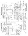
- FIG. 1is a schematic diagram of exemplary dual bus matrix architecture 10 in accordance with the principles of the present invention.
- the architecture 10may be divided into three different areas.
- the first areais a high performance area, such as the 64-bit high performance area shown in FIG. 1 .
- the second areais a standard system area, such as the 32-bit standard system area shown in FIG. 1 .
- the third areais a low throughput area, such as the 32-bit low throughput area shown in FIG. 1 .
- the high performance areacomprises a first interconnect matrix 12 , such as a 64-bit AHB (AMBA High-Performance Bus).
- First interconnect matrix 12has a plurality of master ports (M) and slave ports (S) and is used to directly connect peripherals of very high bandwidth.
- the high performance areapreferably includes a processor 14 , such as a 64-bit core processor (for example, ARM1176).
- Processor 14is connected to two master ports (one instruction port and one for data port) of first matrix 12 .
- a cache controller 16may be connected in between processor 14 and first matrix 12 .
- cache controller 16is an L2 cache controller connected to an L2 cache memory 18 .
- the high performance areamay also include a 64-bit data processing unit 20 connected to one of the master port of first matrix 12 , a 64-bit direct memory access (DMA) assisted peripheral 22 connected to one of the master ports of first matrix 12 , and a 64-bit RAM interface 24 connected to one of the slave ports of first matrix 12 .
- a 64-bit data processing unit 20connected to one of the master port of first matrix 12
- a 64-bit direct memory access (DMA) assisted peripheral 22connected to one of the master ports of first matrix 12
- a 64-bit RAM interface 24connected to one of the slave ports of first matrix 12 .
- a multiport controller 26is connected to at least one of the slave ports of first matrix 12 . As seen in FIG. 1 , one port of controller 26 may be connected to one of the slave ports of first matrix 12 through a 64-bit memory interface 28 , while another port of controller 26 may be connected to another slave port of first matrix 12 through another 64-bit memory interface 30 . In a preferred embodiment, multiport controller 26 is a 64-bit multiport SDR/DDR/DDR2 controller.
- the standard system areacomprises a second interconnect matrix 32 , such as a 32-bit AHB.
- Second interconnect matrix 32has a plurality of slave ports (S) and master ports (M).
- a slave port of that matrixmay be connected to an AHB master port of an AHB master peripheral.
- a master port of that matrixmay be connected to an AHB slave port of an AHB slave peripheral.
- the second interconnect matrixis used to connect peripherals having limited bandwidth requirements.
- a slave port of second interconnect matrix 32may be connected to a slave port of the first interconnect matrix 12 .
- This connectionmay be made through a bridge 34 , such as a 64-bit to 32-bit downsizer.
- the master port of the second interconnect matrix 32may act as a slave port of first interconnect matrix 12 in order to maintain communication between peripherals of both matrices.
- Second interconnect matrix 32may have another master port connected to a multiport DMA controller 36 .
- multiport DMA controller 36is also connected to a master port of first interconnect matrix 12 .
- Yet another master port of second interconnect matrix 32may be connected to a video processing unit 38 .
- video processing unitmay comprise a universal video decoder and/or a graphics accelerator.
- Second interconnect matrix 32may also have a master port used as a video input/output 40 for connection to video devices.
- Such devicesmay include, but are not limited to a camera interface and an LCD controller.
- Another master port of second interconnect matrix 32may be connected to devices used for high-speed communication 42 , such as Ethernet, Universal Serial Bus (USB), and Serial ATA (SATA).
- devices used for high-speed communication 42such as Ethernet, Universal Serial Bus (USB), and Serial ATA (SATA).
- Multiport controller 26is connected to at least one of the slave ports of second matrix 32 .
- the multiport memory controlleracts as a slave peripheral. As seen in FIG. 1 , one port of controller 26 may be connected to one of the slave ports of second matrix 32 through a 32-bit to 64-bit bridge local cache 44 and a 64-bit memory interface 46 , while another port of controller 26 may be connected to another slave port of second matrix 32 through another 32-bit to 64-bit bridge local cache 48 and another 64-bit memory interface 50 .
- the slave ports of second interconnect matrix 32may also be connected to memory devices.
- memory devicesmay include, but are not limited to, a 32-bit SRAM 52 , a 32-bit ROM 54 , and a NAND flash controller 58 .
- Second interconnect matrix 32can also be connected to the low throughput area.
- one of the slave ports of second interconnect matrix 32is connected to a peripheral bus interconnect 60 in the low throughput area through a 32-bit peripheral bridge 56 .
- peripheral bus interconnect 60is a 32-bit peripheral bus interconnect.
- Peripheral bus interconnect 60may be connected to a plurality of low throughput components. These low throughput components may include, but are not limited to, cryptography cores 62 and low speed interfaces 64 .
- cryptography cores 62include Advanced Encryption Standard (AES) and Data Encryption Standard (DES), while examples of low speed interfaces 64 include a Universal Asynchronous Receiver-Transmitter (UART), which is a computer component that handles asynchronous serial communication, and a Serial Peripheral Interface, which is a synchronous serial interface for connecting low/medium-bandwidth external devices.
- UARTUniversal Asynchronous Receiver-Transmitter
- Serial Peripheral Interfacewhich is a synchronous serial interface for connecting low/medium-bandwidth external devices.
- FIG. 2is a flowchart of an exemplary method 200 for accessing the shared memory resource in accordance with the principles of the present invention.
- both high performance master peripherals and limited performance peripheralsmay request from the multiport memory controller access to the shared memory resource through their respective matrices.
- the multiport memory controllergrants access to the shared resource.
- An appropriate resource-dependent scheduling algorithmis used to sort and find the highest pending request among all master requests (if several requests are active at the same time). Then, the access is performed and a chunk of data is read from or written to the shared memory.
- high performance accessis performed through the first interconnect matrix if access is granted.
- limited bandwidth accessis performed through the second interconnect matrix if access is granted.
- the multiport controllerarbitrates between requests until all (both high performance and limited bandwidth) masters are serviced.
- the present inventionuses a shared memory controller to avoid the bottlenecks commonly found in the bridges of the prior art.
- the architectures of the prior artcan be described as being bridge-centric, the architecture of the present invention is centered around the shared memory controller. This design helps provide maximum flexibility of the connections, while maintaining routability between all of the peripherals. If an additional high performance master is required, first interconnect matrix 12 is simply updated by adding a master port. Similarly, if an additional limited bandwidth master, such as a 32-bit standard master, is required, second interconnect matrix 32 is simply updated by adding a master port. There is no need in either situation to add a bridge or a bus.
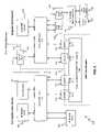
- FIG. 3is a schematic diagram of another exemplary dual bus matrix architecture 300 illustrating the clock domain boundary in accordance with the principles of the present invention.
- Dotted line 336illustrates the boundary between the DDR Clock Domain for the multiport shared memory controller, the Core System Clock Domain for 64-bit high performance, and the 32 System Clock Domain for the 32-bit standard system area.
- the Core System Clock Domaincomprises a first interconnect matrix 302 , such as a 64-bit AHB matrix.
- the Core System Clock Domainalso preferably includes a core processor 304 (such as ARM1176), high performance masters 306 (such as 64-bit AHB masters), and high performance slaves 308 (such as 64-bit AHB slaves) connected to first interconnect matrix 302 .
- the 32 System Clock Domaincomprises a second interconnect matrix 316 , such as a 32-bit AHB matrix.
- First interconnect matrix 302may be connected to second interconnect matrix 316 through a bridge 322 , such as a 64-bit to 32-bit Double Domain Interface.
- the 32 System Clock Domainalso preferably comprises standard masters 324 (such as 32-bit AHB masters) and standard slaves 326 (such as 32-bit AHB slaves) connected to second interconnect matrix 316 .
- the 32 System Clock Domainmay also comprise a peripheral bus interconnect 330 connected to second interconnect matrix 316 through a 32-bit peripheral bridge 328 .
- peripheral bus interconnect 330is a 32-bit peripheral bus interconnect.
- Peripheral bus interconnect 330may be connected to a plurality of components, such as cryptography cores 332 and low speed interfaces 334 .
- the DDR Clock Domaincomprises a multiport shared memory controller 310 , such as a 64-bit multiport SDR/DDR/DDR2 controller.
- First interconnect matrix 302is connected to shared memory controller 310 , such as through Double Domain Interface 312 for port 0 and Double Domain Interface 314 for port 1 .
- Second interconnect matrix 316is also connected to shared memory controller 310 , such as through Double Domain Interface 318 for port 2 and Double Domain Interface 320 for port 3 .
- the different clock domains in the architecture of the present inventionmay be asynchronous.
- the Core System Clock Domainmay run at 133 Mhz, while the 32 System Clock Domain runs at 100 Mhz and the DDR Clock Domain runs at 200 Mhz.
- only a limited regionis running at the maximum frequency.
Landscapes
- Engineering & Computer Science (AREA)
- Theoretical Computer Science (AREA)
- Physics & Mathematics (AREA)
- General Engineering & Computer Science (AREA)
- General Physics & Mathematics (AREA)
- Bus Control (AREA)
- Multi Processors (AREA)
Abstract
Description
Claims (16)
Priority Applications (3)
| Application Number | Priority Date | Filing Date | Title |
|---|---|---|---|
| US11/776,916US7689758B2 (en) | 2007-07-12 | 2007-07-12 | Dual bus matrix architecture for micro-controllers |
| TW097126551ATW200912660A (en) | 2007-07-12 | 2008-07-11 | Dual bus matrix architecture for micro-controllers |
| PCT/US2008/008542WO2009009133A2 (en) | 2007-07-12 | 2008-07-11 | Dual bus system and method |
Applications Claiming Priority (1)
| Application Number | Priority Date | Filing Date | Title |
|---|---|---|---|
| US11/776,916US7689758B2 (en) | 2007-07-12 | 2007-07-12 | Dual bus matrix architecture for micro-controllers |
Publications (2)
| Publication Number | Publication Date |
|---|---|
| US20090019207A1 US20090019207A1 (en) | 2009-01-15 |
| US7689758B2true US7689758B2 (en) | 2010-03-30 |
Family
ID=40229360
Family Applications (1)
| Application Number | Title | Priority Date | Filing Date |
|---|---|---|---|
| US11/776,916Active2027-10-02US7689758B2 (en) | 2007-07-12 | 2007-07-12 | Dual bus matrix architecture for micro-controllers |
Country Status (3)
| Country | Link |
|---|---|
| US (1) | US7689758B2 (en) |
| TW (1) | TW200912660A (en) |
| WO (1) | WO2009009133A2 (en) |
Cited By (2)
| Publication number | Priority date | Publication date | Assignee | Title |
|---|---|---|---|---|
| TWI448900B (en)* | 2010-11-26 | 2014-08-11 | Weltrend Semiconductor Inc | Double parallel bus operation structure |
| US11188483B2 (en) | 2019-11-04 | 2021-11-30 | Hon Hai Precision Industry Co., Ltd. | Architecture for microcontroller and method for reading data applied to microcontroller |
Families Citing this family (4)
| Publication number | Priority date | Publication date | Assignee | Title |
|---|---|---|---|---|
| KR100854973B1 (en)* | 2007-02-13 | 2008-08-28 | 삼성전자주식회사 | System containing a bus matrix |
| US7689758B2 (en) | 2007-07-12 | 2010-03-30 | Atmel Corporation | Dual bus matrix architecture for micro-controllers |
| US20090037629A1 (en)* | 2007-08-01 | 2009-02-05 | Broadcom Corporation | Master slave core architecture with direct buses |
| TWI724608B (en)* | 2019-11-04 | 2021-04-11 | 鴻海精密工業股份有限公司 | Microcontroller architecture and data reading method in architecture |
Citations (19)
| Publication number | Priority date | Publication date | Assignee | Title |
|---|---|---|---|---|
| US4933835A (en) | 1985-02-22 | 1990-06-12 | Intergraph Corporation | Apparatus for maintaining consistency of a cache memory with a primary memory |
| US5091850A (en) | 1987-09-28 | 1992-02-25 | Compaq Computer Corporation | System for fast selection of non-cacheable address ranges using programmed array logic |
| US5157774A (en) | 1987-09-28 | 1992-10-20 | Compaq Computer Corporation | System for fast selection of non-cacheable address ranges using programmed array logic |
| US5438666A (en) | 1988-08-11 | 1995-08-01 | Ast Research, Inc. | Shared memory bus system for arbitrating access control among contending memory refresh circuits, peripheral controllers, and bus masters |
| US5450551A (en) | 1993-05-28 | 1995-09-12 | International Business Machines Corporation | System direct memory access (DMA) support logic for PCI based computer system |
| US5581714A (en) | 1993-05-28 | 1996-12-03 | International Business Machines Corporation | Bus-to-bus read prefetch logic for improving information transfers in a multi-bus information handling system (bus-to-bus bridge for a multiple bus information handling system that optimizes data transfers between a system bus and a peripheral bus) |
| US5710906A (en) | 1995-07-07 | 1998-01-20 | Opti Inc. | Predictive snooping of cache memory for master-initiated accesses |
| US5761443A (en) | 1995-06-07 | 1998-06-02 | Advanced Micro Systems, Inc. | Computer system employing a bus conversion bridge for interfacing a master device residing on a multiplexed peripheral bus to a slave device residing on a split-address, split-data multiplexed peripheral bus |
| US5859651A (en)* | 1996-08-19 | 1999-01-12 | International Business Machines Corporation | Method and apparatus for block data transfer to reduce on-chip storage for interpolative video resizing |
| US20020032820A1 (en) | 2000-09-08 | 2002-03-14 | Jahnke Steve R. | Immediate grant bus arbiter for bus system |
| US20020052995A1 (en) | 2000-09-08 | 2002-05-02 | Jahnke Steven R. | Bus bridge interface system |
| US20020052996A1 (en) | 2000-09-08 | 2002-05-02 | Jahnke Steven R. | Time-out counter for multiple transaction bus system bus bridge |
| US6553446B1 (en) | 1999-09-29 | 2003-04-22 | Silicon Graphics Inc. | Modular input/output controller capable of routing packets over busses operating at different speeds |
| US6775732B2 (en) | 2000-09-08 | 2004-08-10 | Texas Instruments Incorporated | Multiple transaction bus system |
| US20050102455A1 (en) | 2003-11-10 | 2005-05-12 | Oki Electric Industry Co., Ltd. | Data transmission system |
| US20060010260A1 (en) | 2004-07-07 | 2006-01-12 | Fung Hon C | Direct memory access (DMA) controller and bus structure in a master/slave system |
| US7043209B2 (en)* | 2001-07-26 | 2006-05-09 | Kabushiki Kaisha Toshiba | Electronic device and method of mounting radio antenna |
| US20070233429A1 (en) | 2006-02-09 | 2007-10-04 | Atmel Corporation | Apparatus and method for the detection of and recovery from inappropriate bus access in microcontroller circuits |
| WO2009009133A2 (en) | 2007-07-12 | 2009-01-15 | Atmel Corporation | Dual bus system and method |
Family Cites Families (1)
| Publication number | Priority date | Publication date | Assignee | Title |
|---|---|---|---|---|
| US6829689B1 (en)* | 2002-02-12 | 2004-12-07 | Nvidia Corporation | Method and system for memory access arbitration for minimizing read/write turnaround penalties |
- 2007
- 2007-07-12USUS11/776,916patent/US7689758B2/enactiveActive
- 2008
- 2008-07-11WOPCT/US2008/008542patent/WO2009009133A2/enactiveApplication Filing
- 2008-07-11TWTW097126551Apatent/TW200912660A/enunknown
Patent Citations (26)
| Publication number | Priority date | Publication date | Assignee | Title |
|---|---|---|---|---|
| US4933835A (en) | 1985-02-22 | 1990-06-12 | Intergraph Corporation | Apparatus for maintaining consistency of a cache memory with a primary memory |
| US5091850A (en) | 1987-09-28 | 1992-02-25 | Compaq Computer Corporation | System for fast selection of non-cacheable address ranges using programmed array logic |
| US5157774A (en) | 1987-09-28 | 1992-10-20 | Compaq Computer Corporation | System for fast selection of non-cacheable address ranges using programmed array logic |
| US5438666A (en) | 1988-08-11 | 1995-08-01 | Ast Research, Inc. | Shared memory bus system for arbitrating access control among contending memory refresh circuits, peripheral controllers, and bus masters |
| US5450551A (en) | 1993-05-28 | 1995-09-12 | International Business Machines Corporation | System direct memory access (DMA) support logic for PCI based computer system |
| US5581714A (en) | 1993-05-28 | 1996-12-03 | International Business Machines Corporation | Bus-to-bus read prefetch logic for improving information transfers in a multi-bus information handling system (bus-to-bus bridge for a multiple bus information handling system that optimizes data transfers between a system bus and a peripheral bus) |
| US5761443A (en) | 1995-06-07 | 1998-06-02 | Advanced Micro Systems, Inc. | Computer system employing a bus conversion bridge for interfacing a master device residing on a multiplexed peripheral bus to a slave device residing on a split-address, split-data multiplexed peripheral bus |
| US5710906A (en) | 1995-07-07 | 1998-01-20 | Opti Inc. | Predictive snooping of cache memory for master-initiated accesses |
| US5813036A (en) | 1995-07-07 | 1998-09-22 | Opti Inc. | Predictive snooping of cache memory for master-initiated accesses |
| US20040139245A1 (en) | 1995-07-07 | 2004-07-15 | Opti Inc. | Predictive snooping of cache memory for master-initiated accesses |
| US6405291B1 (en) | 1995-07-07 | 2002-06-11 | Opti Inc. | Predictive snooping of cache memory for master-initiated accesses |
| US5859651A (en)* | 1996-08-19 | 1999-01-12 | International Business Machines Corporation | Method and apparatus for block data transfer to reduce on-chip storage for interpolative video resizing |
| US6553446B1 (en) | 1999-09-29 | 2003-04-22 | Silicon Graphics Inc. | Modular input/output controller capable of routing packets over busses operating at different speeds |
| US20020052996A1 (en) | 2000-09-08 | 2002-05-02 | Jahnke Steven R. | Time-out counter for multiple transaction bus system bus bridge |
| US20020052995A1 (en) | 2000-09-08 | 2002-05-02 | Jahnke Steven R. | Bus bridge interface system |
| US6760802B2 (en) | 2000-09-08 | 2004-07-06 | Texas Instruments Incorporated | Time-out counter for multiple transaction bus system bus bridge |
| US20020032820A1 (en) | 2000-09-08 | 2002-03-14 | Jahnke Steve R. | Immediate grant bus arbiter for bus system |
| US6775732B2 (en) | 2000-09-08 | 2004-08-10 | Texas Instruments Incorporated | Multiple transaction bus system |
| US6829669B2 (en) | 2000-09-08 | 2004-12-07 | Texas Instruments Incorporated | Bus bridge interface system |
| US6859852B2 (en) | 2000-09-08 | 2005-02-22 | Texas Instruments Incorporated | Immediate grant bus arbiter for bus system |
| US7043209B2 (en)* | 2001-07-26 | 2006-05-09 | Kabushiki Kaisha Toshiba | Electronic device and method of mounting radio antenna |
| US20050102455A1 (en) | 2003-11-10 | 2005-05-12 | Oki Electric Industry Co., Ltd. | Data transmission system |
| US6940311B2 (en) | 2003-11-10 | 2005-09-06 | Oki Electric Industry Co., Ltd. | Data transmission system |
| US20060010260A1 (en) | 2004-07-07 | 2006-01-12 | Fung Hon C | Direct memory access (DMA) controller and bus structure in a master/slave system |
| US20070233429A1 (en) | 2006-02-09 | 2007-10-04 | Atmel Corporation | Apparatus and method for the detection of and recovery from inappropriate bus access in microcontroller circuits |
| WO2009009133A2 (en) | 2007-07-12 | 2009-01-15 | Atmel Corporation | Dual bus system and method |
Non-Patent Citations (4)
| Title |
|---|
| "International Application Serial No. PCT/US2008/008542, Search Report mailed Dec. 30, 2008". |
| "International Application Serial No. PCT/US2008/008542, Written Opinion mailed Dec. 30, 2008". |
| Mitic, M., et al., "An overview of On- chip buses", Facta universitatis, vol. 19(3), (2006), 405-428. |
| Pasricha, S., et al., "Bus matrix communication architecture synthesis", Center for embedded computer systems, University of California Irvine, (2005). |
Cited By (2)
| Publication number | Priority date | Publication date | Assignee | Title |
|---|---|---|---|---|
| TWI448900B (en)* | 2010-11-26 | 2014-08-11 | Weltrend Semiconductor Inc | Double parallel bus operation structure |
| US11188483B2 (en) | 2019-11-04 | 2021-11-30 | Hon Hai Precision Industry Co., Ltd. | Architecture for microcontroller and method for reading data applied to microcontroller |
Also Published As
| Publication number | Publication date |
|---|---|
| WO2009009133A2 (en) | 2009-01-15 |
| WO2009009133A3 (en) | 2009-02-26 |
| US20090019207A1 (en) | 2009-01-15 |
| TW200912660A (en) | 2009-03-16 |
Similar Documents
| Publication | Publication Date | Title |
|---|---|---|
| US6653859B2 (en) | Heterogeneous integrated circuit with reconfigurable logic cores | |
| CN100499556C (en) | High-speed asynchronous interlinkage communication network of heterogeneous multi-nucleus processor | |
| US12339794B2 (en) | Seamlessly integrated microcontroller chip | |
| US20010042147A1 (en) | System-resource router | |
| JP5079342B2 (en) | Multiprocessor device | |
| US7689758B2 (en) | Dual bus matrix architecture for micro-controllers | |
| US7007111B2 (en) | DMA port sharing bandwidth balancing logic | |
| US20060123152A1 (en) | Inter-processor communication system for communication between processors | |
| US6532511B1 (en) | Asochronous centralized multi-channel DMA controller | |
| US7020733B2 (en) | Data bus system and method for performing cross-access between buses | |
| KR20030056567A (en) | Bus architecture for system on chip with multi-processors and multi-peripherals | |
| KR100475438B1 (en) | Data bus system and method for performing cross-access between buses | |
| Lahtinen et al. | Bus structures in Network-on-Chips | |
| WO2007119373A1 (en) | System controller | |
| KR20100029289A (en) | Multiple bus system and data transmission method using the same |
Legal Events
| Date | Code | Title | Description |
|---|---|---|---|
| AS | Assignment | Owner name:ATMEL CORPORATION, CALIFORNIA Free format text:ASSIGNMENT OF ASSIGNORS INTEREST;ASSIGNOR:TIENNOT, RENAUD;REEL/FRAME:019549/0984 Effective date:20070626 Owner name:ATMEL CORPORATION,CALIFORNIA Free format text:ASSIGNMENT OF ASSIGNORS INTEREST;ASSIGNOR:TIENNOT, RENAUD;REEL/FRAME:019549/0984 Effective date:20070626 | |
| FEPP | Fee payment procedure | Free format text:PAYOR NUMBER ASSIGNED (ORIGINAL EVENT CODE: ASPN); ENTITY STATUS OF PATENT OWNER: LARGE ENTITY | |
| STCF | Information on status: patent grant | Free format text:PATENTED CASE | |
| FPAY | Fee payment | Year of fee payment:4 | |
| AS | Assignment | Owner name:MORGAN STANLEY SENIOR FUNDING, INC. AS ADMINISTRATIVE AGENT, NEW YORK Free format text:PATENT SECURITY AGREEMENT;ASSIGNOR:ATMEL CORPORATION;REEL/FRAME:031912/0173 Effective date:20131206 Owner name:MORGAN STANLEY SENIOR FUNDING, INC. AS ADMINISTRAT Free format text:PATENT SECURITY AGREEMENT;ASSIGNOR:ATMEL CORPORATION;REEL/FRAME:031912/0173 Effective date:20131206 | |
| AS | Assignment | Owner name:ATMEL CORPORATION, CALIFORNIA Free format text:TERMINATION AND RELEASE OF SECURITY INTEREST IN PATENT COLLATERAL;ASSIGNOR:MORGAN STANLEY SENIOR FUNDING, INC.;REEL/FRAME:038376/0001 Effective date:20160404 | |
| AS | Assignment | Owner name:JPMORGAN CHASE BANK, N.A., AS ADMINISTRATIVE AGENT, ILLINOIS Free format text:SECURITY INTEREST;ASSIGNOR:ATMEL CORPORATION;REEL/FRAME:041715/0747 Effective date:20170208 Owner name:JPMORGAN CHASE BANK, N.A., AS ADMINISTRATIVE AGENT Free format text:SECURITY INTEREST;ASSIGNOR:ATMEL CORPORATION;REEL/FRAME:041715/0747 Effective date:20170208 | |
| MAFP | Maintenance fee payment | Free format text:PAYMENT OF MAINTENANCE FEE, 8TH YEAR, LARGE ENTITY (ORIGINAL EVENT CODE: M1552) Year of fee payment:8 | |
| AS | Assignment | Owner name:JPMORGAN CHASE BANK, N.A., AS ADMINISTRATIVE AGENT, ILLINOIS Free format text:SECURITY INTEREST;ASSIGNORS:MICROCHIP TECHNOLOGY INCORPORATED;SILICON STORAGE TECHNOLOGY, INC.;ATMEL CORPORATION;AND OTHERS;REEL/FRAME:046426/0001 Effective date:20180529 Owner name:JPMORGAN CHASE BANK, N.A., AS ADMINISTRATIVE AGENT Free format text:SECURITY INTEREST;ASSIGNORS:MICROCHIP TECHNOLOGY INCORPORATED;SILICON STORAGE TECHNOLOGY, INC.;ATMEL CORPORATION;AND OTHERS;REEL/FRAME:046426/0001 Effective date:20180529 | |
| AS | Assignment | Owner name:WELLS FARGO BANK, NATIONAL ASSOCIATION, AS NOTES COLLATERAL AGENT, CALIFORNIA Free format text:SECURITY INTEREST;ASSIGNORS:MICROCHIP TECHNOLOGY INCORPORATED;SILICON STORAGE TECHNOLOGY, INC.;ATMEL CORPORATION;AND OTHERS;REEL/FRAME:047103/0206 Effective date:20180914 Owner name:WELLS FARGO BANK, NATIONAL ASSOCIATION, AS NOTES C Free format text:SECURITY INTEREST;ASSIGNORS:MICROCHIP TECHNOLOGY INCORPORATED;SILICON STORAGE TECHNOLOGY, INC.;ATMEL CORPORATION;AND OTHERS;REEL/FRAME:047103/0206 Effective date:20180914 | |
| AS | Assignment | Owner name:JPMORGAN CHASE BANK, N.A., AS ADMINISTRATIVE AGENT, DELAWARE Free format text:SECURITY INTEREST;ASSIGNORS:MICROCHIP TECHNOLOGY INC.;SILICON STORAGE TECHNOLOGY, INC.;ATMEL CORPORATION;AND OTHERS;REEL/FRAME:053311/0305 Effective date:20200327 | |
| AS | Assignment | Owner name:MICROSEMI STORAGE SOLUTIONS, INC., ARIZONA Free format text:RELEASE BY SECURED PARTY;ASSIGNOR:JPMORGAN CHASE BANK, N.A, AS ADMINISTRATIVE AGENT;REEL/FRAME:053466/0011 Effective date:20200529 Owner name:MICROCHIP TECHNOLOGY INC., ARIZONA Free format text:RELEASE BY SECURED PARTY;ASSIGNOR:JPMORGAN CHASE BANK, N.A, AS ADMINISTRATIVE AGENT;REEL/FRAME:053466/0011 Effective date:20200529 Owner name:MICROSEMI CORPORATION, CALIFORNIA Free format text:RELEASE BY SECURED PARTY;ASSIGNOR:JPMORGAN CHASE BANK, N.A, AS ADMINISTRATIVE AGENT;REEL/FRAME:053466/0011 Effective date:20200529 Owner name:SILICON STORAGE TECHNOLOGY, INC., ARIZONA Free format text:RELEASE BY SECURED PARTY;ASSIGNOR:JPMORGAN CHASE BANK, N.A, AS ADMINISTRATIVE AGENT;REEL/FRAME:053466/0011 Effective date:20200529 Owner name:ATMEL CORPORATION, ARIZONA Free format text:RELEASE BY SECURED PARTY;ASSIGNOR:JPMORGAN CHASE BANK, N.A, AS ADMINISTRATIVE AGENT;REEL/FRAME:053466/0011 Effective date:20200529 | |
| AS | Assignment | Owner name:WELLS FARGO BANK, NATIONAL ASSOCIATION, MINNESOTA Free format text:SECURITY INTEREST;ASSIGNORS:MICROCHIP TECHNOLOGY INC.;SILICON STORAGE TECHNOLOGY, INC.;ATMEL CORPORATION;AND OTHERS;REEL/FRAME:053468/0705 Effective date:20200529 | |
| AS | Assignment | Owner name:WELLS FARGO BANK, NATIONAL ASSOCIATION, AS COLLATERAL AGENT, MINNESOTA Free format text:SECURITY INTEREST;ASSIGNORS:MICROCHIP TECHNOLOGY INCORPORATED;SILICON STORAGE TECHNOLOGY, INC.;ATMEL CORPORATION;AND OTHERS;REEL/FRAME:055671/0612 Effective date:20201217 | |
| AS | Assignment | Owner name:WELLS FARGO BANK, NATIONAL ASSOCIATION, AS NOTES COLLATERAL AGENT, MINNESOTA Free format text:SECURITY INTEREST;ASSIGNORS:MICROCHIP TECHNOLOGY INCORPORATED;SILICON STORAGE TECHNOLOGY, INC.;ATMEL CORPORATION;AND OTHERS;REEL/FRAME:057935/0474 Effective date:20210528 | |
| MAFP | Maintenance fee payment | Free format text:PAYMENT OF MAINTENANCE FEE, 12TH YEAR, LARGE ENTITY (ORIGINAL EVENT CODE: M1553); ENTITY STATUS OF PATENT OWNER: LARGE ENTITY Year of fee payment:12 | |
| AS | Assignment | Owner name:MICROSEMI STORAGE SOLUTIONS, INC., ARIZONA Free format text:RELEASE BY SECURED PARTY;ASSIGNOR:JPMORGAN CHASE BANK, N.A., AS ADMINISTRATIVE AGENT;REEL/FRAME:059333/0222 Effective date:20220218 Owner name:MICROSEMI CORPORATION, ARIZONA Free format text:RELEASE BY SECURED PARTY;ASSIGNOR:JPMORGAN CHASE BANK, N.A., AS ADMINISTRATIVE AGENT;REEL/FRAME:059333/0222 Effective date:20220218 Owner name:ATMEL CORPORATION, ARIZONA Free format text:RELEASE BY SECURED PARTY;ASSIGNOR:JPMORGAN CHASE BANK, N.A., AS ADMINISTRATIVE AGENT;REEL/FRAME:059333/0222 Effective date:20220218 Owner name:SILICON STORAGE TECHNOLOGY, INC., ARIZONA Free format text:RELEASE BY SECURED PARTY;ASSIGNOR:JPMORGAN CHASE BANK, N.A., AS ADMINISTRATIVE AGENT;REEL/FRAME:059333/0222 Effective date:20220218 Owner name:MICROCHIP TECHNOLOGY INCORPORATED, ARIZONA Free format text:RELEASE BY SECURED PARTY;ASSIGNOR:JPMORGAN CHASE BANK, N.A., AS ADMINISTRATIVE AGENT;REEL/FRAME:059333/0222 Effective date:20220218 | |
| AS | Assignment | Owner name:ATMEL CORPORATION, ARIZONA Free format text:RELEASE BY SECURED PARTY;ASSIGNOR:JPMORGAN CHASE BANK, N.A., AS ADMINISTRATIVE AGENT;REEL/FRAME:059262/0105 Effective date:20220218 | |
| AS | Assignment | Owner name:MICROSEMI STORAGE SOLUTIONS, INC., ARIZONA Free format text:RELEASE BY SECURED PARTY;ASSIGNOR:WELLS FARGO BANK, NATIONAL ASSOCIATION, AS NOTES COLLATERAL AGENT;REEL/FRAME:059358/0001 Effective date:20220228 Owner name:MICROSEMI CORPORATION, ARIZONA Free format text:RELEASE BY SECURED PARTY;ASSIGNOR:WELLS FARGO BANK, NATIONAL ASSOCIATION, AS NOTES COLLATERAL AGENT;REEL/FRAME:059358/0001 Effective date:20220228 Owner name:ATMEL CORPORATION, ARIZONA Free format text:RELEASE BY SECURED PARTY;ASSIGNOR:WELLS FARGO BANK, NATIONAL ASSOCIATION, AS NOTES COLLATERAL AGENT;REEL/FRAME:059358/0001 Effective date:20220228 Owner name:SILICON STORAGE TECHNOLOGY, INC., ARIZONA Free format text:RELEASE BY SECURED PARTY;ASSIGNOR:WELLS FARGO BANK, NATIONAL ASSOCIATION, AS NOTES COLLATERAL AGENT;REEL/FRAME:059358/0001 Effective date:20220228 Owner name:MICROCHIP TECHNOLOGY INCORPORATED, ARIZONA Free format text:RELEASE BY SECURED PARTY;ASSIGNOR:WELLS FARGO BANK, NATIONAL ASSOCIATION, AS NOTES COLLATERAL AGENT;REEL/FRAME:059358/0001 Effective date:20220228 | |
| AS | Assignment | Owner name:MICROSEMI STORAGE SOLUTIONS, INC., ARIZONA Free format text:RELEASE BY SECURED PARTY;ASSIGNOR:WELLS FARGO BANK, NATIONAL ASSOCIATION, AS NOTES COLLATERAL AGENT;REEL/FRAME:059863/0400 Effective date:20220228 Owner name:MICROSEMI CORPORATION, ARIZONA Free format text:RELEASE BY SECURED PARTY;ASSIGNOR:WELLS FARGO BANK, NATIONAL ASSOCIATION, AS NOTES COLLATERAL AGENT;REEL/FRAME:059863/0400 Effective date:20220228 Owner name:ATMEL CORPORATION, ARIZONA Free format text:RELEASE BY SECURED PARTY;ASSIGNOR:WELLS FARGO BANK, NATIONAL ASSOCIATION, AS NOTES COLLATERAL AGENT;REEL/FRAME:059863/0400 Effective date:20220228 Owner name:SILICON STORAGE TECHNOLOGY, INC., ARIZONA Free format text:RELEASE BY SECURED PARTY;ASSIGNOR:WELLS FARGO BANK, NATIONAL ASSOCIATION, AS NOTES COLLATERAL AGENT;REEL/FRAME:059863/0400 Effective date:20220228 Owner name:MICROCHIP TECHNOLOGY INCORPORATED, ARIZONA Free format text:RELEASE BY SECURED PARTY;ASSIGNOR:WELLS FARGO BANK, NATIONAL ASSOCIATION, AS NOTES COLLATERAL AGENT;REEL/FRAME:059863/0400 Effective date:20220228 | |
| AS | Assignment | Owner name:MICROSEMI STORAGE SOLUTIONS, INC., ARIZONA Free format text:RELEASE BY SECURED PARTY;ASSIGNOR:WELLS FARGO BANK, NATIONAL ASSOCIATION, AS NOTES COLLATERAL AGENT;REEL/FRAME:059363/0001 Effective date:20220228 Owner name:MICROSEMI CORPORATION, ARIZONA Free format text:RELEASE BY SECURED PARTY;ASSIGNOR:WELLS FARGO BANK, NATIONAL ASSOCIATION, AS NOTES COLLATERAL AGENT;REEL/FRAME:059363/0001 Effective date:20220228 Owner name:ATMEL CORPORATION, ARIZONA Free format text:RELEASE BY SECURED PARTY;ASSIGNOR:WELLS FARGO BANK, NATIONAL ASSOCIATION, AS NOTES COLLATERAL AGENT;REEL/FRAME:059363/0001 Effective date:20220228 Owner name:SILICON STORAGE TECHNOLOGY, INC., ARIZONA Free format text:RELEASE BY SECURED PARTY;ASSIGNOR:WELLS FARGO BANK, NATIONAL ASSOCIATION, AS NOTES COLLATERAL AGENT;REEL/FRAME:059363/0001 Effective date:20220228 Owner name:MICROCHIP TECHNOLOGY INCORPORATED, ARIZONA Free format text:RELEASE BY SECURED PARTY;ASSIGNOR:WELLS FARGO BANK, NATIONAL ASSOCIATION, AS NOTES COLLATERAL AGENT;REEL/FRAME:059363/0001 Effective date:20220228 | |
| AS | Assignment | Owner name:MICROSEMI STORAGE SOLUTIONS, INC., ARIZONA Free format text:RELEASE BY SECURED PARTY;ASSIGNOR:WELLS FARGO BANK, NATIONAL ASSOCIATION, AS NOTES COLLATERAL AGENT;REEL/FRAME:060894/0437 Effective date:20220228 Owner name:MICROSEMI CORPORATION, ARIZONA Free format text:RELEASE BY SECURED PARTY;ASSIGNOR:WELLS FARGO BANK, NATIONAL ASSOCIATION, AS NOTES COLLATERAL AGENT;REEL/FRAME:060894/0437 Effective date:20220228 Owner name:ATMEL CORPORATION, ARIZONA Free format text:RELEASE BY SECURED PARTY;ASSIGNOR:WELLS FARGO BANK, NATIONAL ASSOCIATION, AS NOTES COLLATERAL AGENT;REEL/FRAME:060894/0437 Effective date:20220228 Owner name:SILICON STORAGE TECHNOLOGY, INC., ARIZONA Free format text:RELEASE BY SECURED PARTY;ASSIGNOR:WELLS FARGO BANK, NATIONAL ASSOCIATION, AS NOTES COLLATERAL AGENT;REEL/FRAME:060894/0437 Effective date:20220228 Owner name:MICROCHIP TECHNOLOGY INCORPORATED, ARIZONA Free format text:RELEASE BY SECURED PARTY;ASSIGNOR:WELLS FARGO BANK, NATIONAL ASSOCIATION, AS NOTES COLLATERAL AGENT;REEL/FRAME:060894/0437 Effective date:20220228 |