US7688206B2 - Radio frequency identification (RFID) tag for an item having a conductive layer included or attached - Google Patents
Radio frequency identification (RFID) tag for an item having a conductive layer included or attachedDownload PDFInfo
- Publication number
- US7688206B2 US7688206B2US11/033,347US3334705AUS7688206B2US 7688206 B2US7688206 B2US 7688206B2US 3334705 AUS3334705 AUS 3334705AUS 7688206 B2US7688206 B2US 7688206B2
- Authority
- US
- United States
- Prior art keywords
- rfid
- integrated circuit
- conductive layer
- circuit chip
- layer
- Prior art date
- Legal status (The legal status is an assumption and is not a legal conclusion. Google has not performed a legal analysis and makes no representation as to the accuracy of the status listed.)
- Expired - Fee Related, expires
Links
Images


Classifications
- G—PHYSICS
- G06—COMPUTING OR CALCULATING; COUNTING
- G06K—GRAPHICAL DATA READING; PRESENTATION OF DATA; RECORD CARRIERS; HANDLING RECORD CARRIERS
- G06K19/00—Record carriers for use with machines and with at least a part designed to carry digital markings
- G06K19/06—Record carriers for use with machines and with at least a part designed to carry digital markings characterised by the kind of the digital marking, e.g. shape, nature, code
- G06K19/067—Record carriers with conductive marks, printed circuits or semiconductor circuit elements, e.g. credit or identity cards also with resonating or responding marks without active components
- G06K19/07—Record carriers with conductive marks, printed circuits or semiconductor circuit elements, e.g. credit or identity cards also with resonating or responding marks without active components with integrated circuit chips
- G06K19/0723—Record carriers with conductive marks, printed circuits or semiconductor circuit elements, e.g. credit or identity cards also with resonating or responding marks without active components with integrated circuit chips the record carrier comprising an arrangement for non-contact communication, e.g. wireless communication circuits on transponder cards, non-contact smart cards or RFIDs
- G—PHYSICS
- G06—COMPUTING OR CALCULATING; COUNTING
- G06K—GRAPHICAL DATA READING; PRESENTATION OF DATA; RECORD CARRIERS; HANDLING RECORD CARRIERS
- G06K19/00—Record carriers for use with machines and with at least a part designed to carry digital markings
- G06K19/06—Record carriers for use with machines and with at least a part designed to carry digital markings characterised by the kind of the digital marking, e.g. shape, nature, code
- G06K19/067—Record carriers with conductive marks, printed circuits or semiconductor circuit elements, e.g. credit or identity cards also with resonating or responding marks without active components
- G06K19/07—Record carriers with conductive marks, printed circuits or semiconductor circuit elements, e.g. credit or identity cards also with resonating or responding marks without active components with integrated circuit chips
- G06K19/077—Constructional details, e.g. mounting of circuits in the carrier
- G06K19/07749—Constructional details, e.g. mounting of circuits in the carrier the record carrier being capable of non-contact communication, e.g. constructional details of the antenna of a non-contact smart card
- G06K19/07773—Antenna details
- G06K19/07788—Antenna details the antenna being of the capacitive type
- G—PHYSICS
- G08—SIGNALLING
- G08B—SIGNALLING OR CALLING SYSTEMS; ORDER TELEGRAPHS; ALARM SYSTEMS
- G08B13/00—Burglar, theft or intruder alarms
- G08B13/22—Electrical actuation
- G08B13/24—Electrical actuation by interference with electromagnetic field distribution
- G08B13/2402—Electronic Article Surveillance [EAS], i.e. systems using tags for detecting removal of a tagged item from a secure area, e.g. tags for detecting shoplifting
- G08B13/2405—Electronic Article Surveillance [EAS], i.e. systems using tags for detecting removal of a tagged item from a secure area, e.g. tags for detecting shoplifting characterised by the tag technology used
- G08B13/2414—Electronic Article Surveillance [EAS], i.e. systems using tags for detecting removal of a tagged item from a secure area, e.g. tags for detecting shoplifting characterised by the tag technology used using inductive tags
- G08B13/2417—Electronic Article Surveillance [EAS], i.e. systems using tags for detecting removal of a tagged item from a secure area, e.g. tags for detecting shoplifting characterised by the tag technology used using inductive tags having a radio frequency identification chip
- G—PHYSICS
- G08—SIGNALLING
- G08B—SIGNALLING OR CALLING SYSTEMS; ORDER TELEGRAPHS; ALARM SYSTEMS
- G08B13/00—Burglar, theft or intruder alarms
- G08B13/22—Electrical actuation
- G08B13/24—Electrical actuation by interference with electromagnetic field distribution
- G08B13/2402—Electronic Article Surveillance [EAS], i.e. systems using tags for detecting removal of a tagged item from a secure area, e.g. tags for detecting shoplifting
- G08B13/2428—Tag details
- G08B13/2437—Tag layered structure, processes for making layered tags
- G08B13/2445—Tag integrated into item to be protected, e.g. source tagging
- H—ELECTRICITY
- H01—ELECTRIC ELEMENTS
- H01L—SEMICONDUCTOR DEVICES NOT COVERED BY CLASS H10
- H01L24/00—Arrangements for connecting or disconnecting semiconductor or solid-state bodies; Methods or apparatus related thereto
- H01L24/01—Means for bonding being attached to, or being formed on, the surface to be connected, e.g. chip-to-package, die-attach, "first-level" interconnects; Manufacturing methods related thereto
- H01L24/18—High density interconnect [HDI] connectors; Manufacturing methods related thereto
- H01L24/23—Structure, shape, material or disposition of the high density interconnect connectors after the connecting process
- H01L24/24—Structure, shape, material or disposition of the high density interconnect connectors after the connecting process of an individual high density interconnect connector
- H—ELECTRICITY
- H01—ELECTRIC ELEMENTS
- H01L—SEMICONDUCTOR DEVICES NOT COVERED BY CLASS H10
- H01L24/00—Arrangements for connecting or disconnecting semiconductor or solid-state bodies; Methods or apparatus related thereto
- H01L24/80—Methods for connecting semiconductor or other solid state bodies using means for bonding being attached to, or being formed on, the surface to be connected
- H01L24/82—Methods for connecting semiconductor or other solid state bodies using means for bonding being attached to, or being formed on, the surface to be connected by forming build-up interconnects at chip-level, e.g. for high density interconnects [HDI]
- H—ELECTRICITY
- H01—ELECTRIC ELEMENTS
- H01L—SEMICONDUCTOR DEVICES NOT COVERED BY CLASS H10
- H01L2224/00—Indexing scheme for arrangements for connecting or disconnecting semiconductor or solid-state bodies and methods related thereto as covered by H01L24/00
- H01L2224/01—Means for bonding being attached to, or being formed on, the surface to be connected, e.g. chip-to-package, die-attach, "first-level" interconnects; Manufacturing methods related thereto
- H01L2224/18—High density interconnect [HDI] connectors; Manufacturing methods related thereto
- H01L2224/23—Structure, shape, material or disposition of the high density interconnect connectors after the connecting process
- H01L2224/24—Structure, shape, material or disposition of the high density interconnect connectors after the connecting process of an individual high density interconnect connector
- H01L2224/241—Disposition
- H01L2224/24151—Connecting between a semiconductor or solid-state body and an item not being a semiconductor or solid-state body, e.g. chip-to-substrate, chip-to-passive
- H01L2224/24221—Connecting between a semiconductor or solid-state body and an item not being a semiconductor or solid-state body, e.g. chip-to-substrate, chip-to-passive the body and the item being stacked
- H01L2224/24225—Connecting between a semiconductor or solid-state body and an item not being a semiconductor or solid-state body, e.g. chip-to-substrate, chip-to-passive the body and the item being stacked the item being non-metallic, e.g. insulating substrate with or without metallisation
- H01L2224/24227—Connecting between a semiconductor or solid-state body and an item not being a semiconductor or solid-state body, e.g. chip-to-substrate, chip-to-passive the body and the item being stacked the item being non-metallic, e.g. insulating substrate with or without metallisation the HDI interconnect not connecting to the same level of the item at which the semiconductor or solid-state body is mounted, e.g. the semiconductor or solid-state body being mounted in a cavity or on a protrusion of the item
- H—ELECTRICITY
- H01—ELECTRIC ELEMENTS
- H01L—SEMICONDUCTOR DEVICES NOT COVERED BY CLASS H10
- H01L2224/00—Indexing scheme for arrangements for connecting or disconnecting semiconductor or solid-state bodies and methods related thereto as covered by H01L24/00
- H01L2224/74—Apparatus for manufacturing arrangements for connecting or disconnecting semiconductor or solid-state bodies and for methods related thereto
- H01L2224/76—Apparatus for connecting with build-up interconnects
- H01L2224/7665—Means for transporting the components to be connected
- H—ELECTRICITY
- H01—ELECTRIC ELEMENTS
- H01L—SEMICONDUCTOR DEVICES NOT COVERED BY CLASS H10
- H01L2224/00—Indexing scheme for arrangements for connecting or disconnecting semiconductor or solid-state bodies and methods related thereto as covered by H01L24/00
- H01L2224/80—Methods for connecting semiconductor or other solid state bodies using means for bonding being attached to, or being formed on, the surface to be connected
- H01L2224/82—Methods for connecting semiconductor or other solid state bodies using means for bonding being attached to, or being formed on, the surface to be connected by forming build-up interconnects at chip-level, e.g. for high density interconnects [HDI]
- H01L2224/82009—Pre-treatment of the connector or the bonding area
- H01L2224/8203—Reshaping, e.g. forming vias
- H01L2224/82035—Reshaping, e.g. forming vias by heating means
- H01L2224/82039—Reshaping, e.g. forming vias by heating means using a laser
- H—ELECTRICITY
- H01—ELECTRIC ELEMENTS
- H01L—SEMICONDUCTOR DEVICES NOT COVERED BY CLASS H10
- H01L2224/00—Indexing scheme for arrangements for connecting or disconnecting semiconductor or solid-state bodies and methods related thereto as covered by H01L24/00
- H01L2224/93—Batch processes
- H01L2224/95—Batch processes at chip-level, i.e. with connecting carried out on a plurality of singulated devices, i.e. on diced chips
- H01L2224/95053—Bonding environment
- H01L2224/95085—Bonding environment being a liquid, e.g. for fluidic self-assembly
- H—ELECTRICITY
- H01—ELECTRIC ELEMENTS
- H01L—SEMICONDUCTOR DEVICES NOT COVERED BY CLASS H10
- H01L2224/00—Indexing scheme for arrangements for connecting or disconnecting semiconductor or solid-state bodies and methods related thereto as covered by H01L24/00
- H01L2224/93—Batch processes
- H01L2224/95—Batch processes at chip-level, i.e. with connecting carried out on a plurality of singulated devices, i.e. on diced chips
- H01L2224/9512—Aligning the plurality of semiconductor or solid-state bodies
- H01L2224/95136—Aligning the plurality of semiconductor or solid-state bodies involving guiding structures, e.g. shape matching, spacers or supporting members
- H—ELECTRICITY
- H01—ELECTRIC ELEMENTS
- H01L—SEMICONDUCTOR DEVICES NOT COVERED BY CLASS H10
- H01L2924/00—Indexing scheme for arrangements or methods for connecting or disconnecting semiconductor or solid-state bodies as covered by H01L24/00
- H01L2924/01—Chemical elements
- H01L2924/01027—Cobalt [Co]
- H—ELECTRICITY
- H01—ELECTRIC ELEMENTS
- H01L—SEMICONDUCTOR DEVICES NOT COVERED BY CLASS H10
- H01L2924/00—Indexing scheme for arrangements or methods for connecting or disconnecting semiconductor or solid-state bodies as covered by H01L24/00
- H01L2924/01—Chemical elements
- H01L2924/01033—Arsenic [As]
- H—ELECTRICITY
- H01—ELECTRIC ELEMENTS
- H01L—SEMICONDUCTOR DEVICES NOT COVERED BY CLASS H10
- H01L2924/00—Indexing scheme for arrangements or methods for connecting or disconnecting semiconductor or solid-state bodies as covered by H01L24/00
- H01L2924/01—Chemical elements
- H01L2924/01075—Rhenium [Re]
- H—ELECTRICITY
- H01—ELECTRIC ELEMENTS
- H01L—SEMICONDUCTOR DEVICES NOT COVERED BY CLASS H10
- H01L2924/00—Indexing scheme for arrangements or methods for connecting or disconnecting semiconductor or solid-state bodies as covered by H01L24/00
- H01L2924/013—Alloys
- H01L2924/014—Solder alloys
- H—ELECTRICITY
- H01—ELECTRIC ELEMENTS
- H01L—SEMICONDUCTOR DEVICES NOT COVERED BY CLASS H10
- H01L2924/00—Indexing scheme for arrangements or methods for connecting or disconnecting semiconductor or solid-state bodies as covered by H01L24/00
- H01L2924/10—Details of semiconductor or other solid state devices to be connected
- H01L2924/11—Device type
- H01L2924/12—Passive devices, e.g. 2 terminal devices
- H01L2924/1204—Optical Diode
- H01L2924/12042—LASER
- H—ELECTRICITY
- H01—ELECTRIC ELEMENTS
- H01L—SEMICONDUCTOR DEVICES NOT COVERED BY CLASS H10
- H01L2924/00—Indexing scheme for arrangements or methods for connecting or disconnecting semiconductor or solid-state bodies as covered by H01L24/00
- H01L2924/10—Details of semiconductor or other solid state devices to be connected
- H01L2924/11—Device type
- H01L2924/14—Integrated circuits
- H—ELECTRICITY
- H01—ELECTRIC ELEMENTS
- H01L—SEMICONDUCTOR DEVICES NOT COVERED BY CLASS H10
- H01L2924/00—Indexing scheme for arrangements or methods for connecting or disconnecting semiconductor or solid-state bodies as covered by H01L24/00
- H01L2924/15—Details of package parts other than the semiconductor or other solid state devices to be connected
- H01L2924/151—Die mounting substrate
- H01L2924/1515—Shape
- H01L2924/15153—Shape the die mounting substrate comprising a recess for hosting the device
- H01L2924/15155—Shape the die mounting substrate comprising a recess for hosting the device the shape of the recess being other than a cuboid
- H—ELECTRICITY
- H01—ELECTRIC ELEMENTS
- H01L—SEMICONDUCTOR DEVICES NOT COVERED BY CLASS H10
- H01L2924/00—Indexing scheme for arrangements or methods for connecting or disconnecting semiconductor or solid-state bodies as covered by H01L24/00
- H01L2924/15—Details of package parts other than the semiconductor or other solid state devices to be connected
- H01L2924/151—Die mounting substrate
- H01L2924/15165—Monolayer substrate
- Y—GENERAL TAGGING OF NEW TECHNOLOGICAL DEVELOPMENTS; GENERAL TAGGING OF CROSS-SECTIONAL TECHNOLOGIES SPANNING OVER SEVERAL SECTIONS OF THE IPC; TECHNICAL SUBJECTS COVERED BY FORMER USPC CROSS-REFERENCE ART COLLECTIONS [XRACs] AND DIGESTS
- Y10—TECHNICAL SUBJECTS COVERED BY FORMER USPC
- Y10T—TECHNICAL SUBJECTS COVERED BY FORMER US CLASSIFICATION
- Y10T29/00—Metal working
- Y10T29/49—Method of mechanical manufacture
- Y10T29/49002—Electrical device making
- Y10T29/49016—Antenna or wave energy "plumbing" making
- Y—GENERAL TAGGING OF NEW TECHNOLOGICAL DEVELOPMENTS; GENERAL TAGGING OF CROSS-SECTIONAL TECHNOLOGIES SPANNING OVER SEVERAL SECTIONS OF THE IPC; TECHNICAL SUBJECTS COVERED BY FORMER USPC CROSS-REFERENCE ART COLLECTIONS [XRACs] AND DIGESTS
- Y10—TECHNICAL SUBJECTS COVERED BY FORMER USPC
- Y10T—TECHNICAL SUBJECTS COVERED BY FORMER US CLASSIFICATION
- Y10T29/00—Metal working
- Y10T29/49—Method of mechanical manufacture
- Y10T29/49002—Electrical device making
- Y10T29/49117—Conductor or circuit manufacturing
- Y10T29/49124—On flat or curved insulated base, e.g., printed circuit, etc.
- Y10T29/49128—Assembling formed circuit to base
- Y—GENERAL TAGGING OF NEW TECHNOLOGICAL DEVELOPMENTS; GENERAL TAGGING OF CROSS-SECTIONAL TECHNOLOGIES SPANNING OVER SEVERAL SECTIONS OF THE IPC; TECHNICAL SUBJECTS COVERED BY FORMER USPC CROSS-REFERENCE ART COLLECTIONS [XRACs] AND DIGESTS
- Y10—TECHNICAL SUBJECTS COVERED BY FORMER USPC
- Y10T—TECHNICAL SUBJECTS COVERED BY FORMER US CLASSIFICATION
- Y10T29/00—Metal working
- Y10T29/49—Method of mechanical manufacture
- Y10T29/49002—Electrical device making
- Y10T29/49117—Conductor or circuit manufacturing
- Y10T29/49124—On flat or curved insulated base, e.g., printed circuit, etc.
- Y10T29/49155—Manufacturing circuit on or in base
Definitions
- the present inventionrelates generally to incorporating a radio frequency (RF) transponder into a device to allow tagging for the device using an RFID system.
- RFradio frequency
- RFRadio Frequency
- the RF transponderincludes a memory component that can store particular information, such as identification information (e.g., price, identification, serial number, product information, etc . . . ) about the object or the item.
- identification informatione.g., price, identification, serial number, product information, etc . . .
- Many RFID systemsoperate based on a passive powering system in which the RFID reader conveys energy to the RFID transponder.
- the RF transponderincludes an antenna to receive the energy conveyed from the RFID reader and transfer the energy to the memory component in order to facilitate the communication between the RF reader and the RF transponder.
- Some systemsinclude both “read” and “write” functions; thus, the RF reader can read information previously stored in the RF transponder's memory and the RF transponder can also write new information into the memory in response to signals from the RF reader.
- Each RF transponderhas an individual code containing information related to and identifying the associated object/item.
- the RF readersends an RF signal to the remote RF transponder.
- the antenna in the RF transponderreceives the signal from the RF reader, backscatter-modulates the received signal with data temporarily or permanently stored in the RF transponder (such as data indicating the identity prices, and/or contents of the object/item to which the transponder is attached), produces a sequence of signals in accordance with the transponder's individual code, and reflects this modulated signal back to the RF reader to pass the information contained in the RF transponder to the RF reader.
- the RF readerdecodes these signals to obtain the information from the transponder.
- the transpondermay decode signals received from the reader and write information to the transponder's memory.
- Tagging an object or an itemis an important application. Tagging an object or an item includes at least identifying, authenticating, recognizing, inventorying, checking-in, checking-out, tracking, locating, detecting and sensing the electronic device for many purposes. For instance, there have been many attempts to tag an item such as a CD or a DVD.CD, a DVD, a merchandise, or the like. Such tagging has been employing an RFID system. Attempts have been made to place an RFID transponder on the cover or jacket of the CD or the DVD item. However, current tagging technology employing RFID systems do not successfully read the items/objects 100% of the time, especially without adding complex components to the items to booster the read accuracy.
- the transponderis only placed on the jacket or cover of the item such as CDs/DVDs thus allowing for possible removal or tampering of the RFID transponder and possibly removing the CDs/DVDs from actual item from the jackets or the covers. Such possible removal the actual CDs or DVDs items from the covers defeat the purpose of tagging.
- the current tagging technologyemploys only a short range detection (13.56 MHz) thus does not provide for a long range detection.
- Embodiments of the present inventionpertain to an RFID transponder/tag for an item having a conductive layer included therein.
- Many itemscurrently include a conductive layer in its label, packaging, protective cover, sealing cover, or the like. Examples of such an item may include a Blister Pack, a pharmaceutical item, a medicine bottle, an electronic item, a packaging of an item, food, toy, electronic, or non-electronic item in a package, or any other item that can incorporates or has a conductive layer.
- Embodiments of the present inventionleverage the conductive layer that may already currently being included with certain items to incorporate an RFID tag into the items.
- Some embodimentsincorporate an RFID tag into an item that includes the conductive layer in which the conductive layer is configured such that it can function as an antenna for an RFID tag.
- One embodiment of the inventionpertains to a device that comprises a conductive layer (e.g., foil or metal) formed on a first substrate.
- An opening line(or two or more opening lines) is formed in the conductive layer to make the conductive layer a part of an antenna structure.
- An integrated circuit chipis placed over at least a portion the opening line and interconnected to the conductive layer.
- the devicecan be a Blister Pack, a bottle cap, a bottle sealing, or an object that can incorporates/includes the conductive layer.
- One embodiment of the inventionpertains to a method that comprises creating an opening line in a conductive layer formed on a first substrate and coupling a RFID integrated circuit chip to the conductive layer.
- the opening lineenables the conductive layer to act as a part of an antenna structure for an RFID device.
- the RFID integrated circuit chipis placed over a portion of the opening line and is electrically interconnected to the conductive layer.
- the methodenables tagging, authenticating, and/or tracking an item that includes that conductive layer and the RFID integrated circuit chip assembled according to embodiments of the present invention.
- An RFID tag readeris provided so that information stored in the RFID integrated circuit chip can be transferred to and from the RFID integrated circuit chip.
- the RFID tag readeris also provided so that the conductive layer can receive energy from the reader to provide power to the RFID integrated circuit chip so that the chip can effectuate communication between the RFID device and the RFID reader.
- the RFID deviceis formed using a web process.
- the conductive layeracts as an antenna for an RFID device.
- a cap layeris placed over the conductive layer and the RFID integrated circuit chip.
- the integrated circuit chipis recessed into a second substrate, which is then coupled to the conductive layer such that the integrated circuit chip is interconnected to the conductive layer.
- the integrated circuit chipmay also be recessed into the second substrate via a fluidic-self-assembly (FSA) process.
- FSAfluidic-self-assembly
- the integrated circuit chipmay also be recessed below a surface of the second substrate.
- an RFID tagis incorporated into an item that includes a conductive layer or a metalization layer that provides an electrical function for the item (e.g., as in the case of a CD or a DVID disc).
- the conductive layer for such itemthus cannot be altered since the conductive layer needs to still perform the electrical function for the item.
- the RFID tagis incorporated into the item using capacitive coupling to the conductive layer.
- One embodiment of the inventionpertains to a device that comprises a metalization layer and an integrated circuit chip incorporated into the device wherein the integrated circuit chip is capacitively coupled to the metalization layer.
- the devicecomprises a first substrate having the metalization layer formed on the substrate, a cap layer covering at least the entire metalization layer and at least a portion of the substrate not covered by the metalization layer.
- the integrated circuit chipis coupled to the first substrate, and is placed in proximity and in non-physical contact with the metalization layer.
- a conductive layeris attached to the integrated circuit chip.
- the conductive layerhas at least a portion placed in a non-physical contact with the metalization layer.
- the integrated circuit chipis capacitively coupled to the metalization layer through the conductive layer and the metalization layer.
- the integrated circuit chipis an RFID chip in one embodiment and the metalization layer acts as the antenna that is coupled to the RFID chip capacitively for an RFID system.
- the devicecan be a CD, CD-ROM, CD-R, CD-RW, CD-I, DVD, DVD-ROM, DVD-R, and DVD-RAM.
- One embodiment of the inventionpertains to a device that comprises a metalization layer and an integrated circuit chip incorporated into a label that is affixed to the device wherein the integrated circuit chip is capacitively coupled to the metalization layer.
- the devicecomprises a first substrate having the metalization layer formed on the substrate. A cap layer covering at least the entire metalization layer. At least a portion of the substrate is not covered by the metalization layer.
- the labelis placed over the substrate.
- the integrated circuit chipis coupled to the label.
- the integrated circuit chipis placed in proximity and in non-physical contact with the metalization layer.
- a conductive layeris attached to the integrated circuit chip.
- the conductive layerhas at least a portion placed in a non-physical contact with the metalization layer.
- the integrated circuit chipis capacitively coupled to the metalization layer through the conductive layer and the metalization layer.
- the integrated circuit chipis an RFID chip in one embodiment and the metalization layer acts as the antenna that is coupled to the RFID chip capacitively for an RFID system.
- the devicecan be a CD, CD-ROM, CD-R, CD-RW, CD-I, DVD, DVD-ROM, DVD-R, and DVD-RAM.
- One embodiment of the inventionpertains to a device that comprises a metalization layer and an integrated circuit chip incorporated into a center ring substrate that is affixed to the center of the device wherein the integrated circuit chip is capacitively coupled to the metalization layer.
- the devicecomprises a first substrate having the metalization layer formed on the substrate.
- a cap layercovers at least the entire metalization layer. At least a central portion of the substrate is not covered by the metalization layer.
- the center ring substrateis placed over the central portion.
- the center ring substratecomprises the integrated circuit chip disposed therein, a conductive layer attached to the integrated circuit chip, and may have one or more weight balancing components.
- the integrated circuit chipis placed such that the integrated circuit chip is in proximity and in non-physical contact with the metalization layer.
- the conductive layerhas at least a portion placed in a non-physical contact with the metalization layer.
- the integrated circuit chipis capacitively or inductively coupled to the metalization layer through the conductive layer and the metalization layer.
- the integrated circuit chipis an RFID chip in one embodiment and the metalization layer acts as the antenna that is coupled to the RFID chip capacitively for an RFID system.
- the devicecan be a CD, CD-ROM, CD-R, CD-RW, CD-I, DVD, DVD-ROM, DVD-R, and DVD-RAM.
- inventions of the present inventionpertain to methods which comprise providing an electronic device.
- the electronic devicecomprises a first substrate having a metalization layer formed on the substrate, a cap layer covering at least all of the metalization layer and at least a portion of the substrate is not covered by the metalization layer.
- the methodsfurther comprise providing an RFID transponder, which comprises identification information for the electronic device, and providing an RFID reader receptive of the RFID transponder.
- the RFID transponderis incorporated into the electronic device.
- the RFID transponderincludes an integrated circuit chip coupled to the first substrate and placed in proximity and in non-physical contact with the metalization layer and a conductive layer attached to the integrated circuit chip and having at least a portion placed in a non-physical contact with the metalization layer.
- the integrated circuit chipis capacitively or inductively coupled to the metalization layer through the conductive layer and the metalization layer.
- the RFID transponderincludes a label placed over the substrate, an integrated circuit chip coupled to the label, and a conductive layer attached to the integrated circuit chip.
- the integrated circuit chipis placed in proximity and in non-physical contact with the metalization layer.
- the conductive layerhas at least a portion placed in a non-physical contact with the metalization layer.
- the integrated circuit chipis capacitively or inductively coupled to the metalization layer through the conductive layer and the metalization layer.
- the center ring substratecomprises an integrated circuit chip disposed therein.
- a conductive layeris attached to the integrated circuit chip.
- One or more weight balancing componentsmay be deposited on the center ring substrate.
- the integrated circuit chipis placed such that the integrated circuit chip is in proximity and in non-physical contact with the metalization layer.
- the conductive layerhas at least a portion placed in a non-physical contact with the metalization layer.
- the integrated circuit chipis capacitively or inductively coupled to the metalization layer through the conductive layer and the metalization layer.
- FIGS. 1A-1Billustrate an exemplary device that can incorporate an RFID transponder
- FIG. 2illustrates an exemplary RFID transponder incorporated into a device through capacitive coupling
- FIG. 3illustrates an exemplary RFID circuit chip in the form of a functional block
- FIG. 4illustrates another exemplary RFID circuit chip in the form of a functional block
- FIG. 5illustrates an exemplary RFID transponder incorporated into a device through capacitive coupling
- FIGS. 6-12illustrate exemplary configurations of a conductive layer coupled to an RFID circuit chip
- FIGS. 13-14illustrate an exemplary device that directly incorporates an RFID transponder
- FIGS. 15-23illustrate other exemplary devices that directly incorporates an RFID transponder
- FIG. 24illustrates an exemplary method of identifying a device that incorporates an RFID transponder
- FIG. 25illustrates an exemplary playback system for use in one exemplary aspect of the present invention
- FIG. 26illustrates an exemplary Blister Pack that can benefit from various embodiments of the present invention
- FIG. 27illustrates an exemplary bottle that can benefit from various embodiments of the present invention
- FIGS. 28-29illustrate an exemplary embodiment of incorporating an RFID transponder into an item in accordance to embodiments of the present invention
- FIGS. 30-31illustrate an exemplary embodiment of incorporating an RFID transponder into a Blister Pack in accordance with embodiments of the present invention
- FIGS. 32-33illustrate an exemplary embodiment of incorporating an RFID transponder into a bottle in accordance with embodiments of the present invention
- FIG. 34illustrates an exemplary process of incorporating an RFID transponder into an item in accordance with embodiments of the present invention
- FIG. 35illustrates another exemplary process of incorporating an RFID transponder into an item in accordance with embodiments of the present invention.
- FIG. 36illustrates yet another exemplary process of incorporating an RFID transponder into an item in accordance with embodiments of the present invention.
- Embodiments of the present inventionpertain to an RFID transponder (tag) incorporated into a device, an item, and an object, such as an electronic device, a food item, a medicine bottle, a Blister Pack, a book, or any other item that allows a conductive layer to be attached thereto or included therein.
- Embodiments of the present inventionalso pertain to methods of tagging, identifying, or authenticating a particular item using the RFID transponder that is incorporated into the item.
- RFID devicesare currently used for remote identification of objects.
- the ability to remotely identify or detect an item using an RFID systemis important for many purposes such as identifying/detecting an item or an object in a warehouse, retailers, stores, pharmacies, hospitals, drug stores, supermarkets, libraries, dealerships, parking lots, airports, train stations, and/or at many other locations.
- An RFID systemneeds an RFID reader and an RFID transponder (tag).
- An antennais typically formed on the RFID transponder as is know in the art. Manufacturers have been unable to make or place an RFID transponder directly on a device that has a metal structure included therein because an antenna structure or loop cannot be printed on the metal and still function properly.
- CDCompact Disc
- CD-ROMCompact Disc Read Only Memory
- CD-RCompact Disc Recordable
- CD-RWCompact Disc Rewritable
- CD-ICompact Disc Interactive
- DVDDigital Video Disc or Digital Versatile Disc
- DVD-ROMDigital Video Disc Read Only
- DVD-RDigital Video Disc Recordable
- DVD-RAMDigital Video Disc Rewritable
- manufacturershave been unable to incorporate an RFID transponder into a pharmaceutical packaging without substantial and costly modification (e.g., a Blister Pack or a bottle) since currently many of these pharmaceutical packaging include a conductive component.
- a RFID transponderdirectly on such devices is that the antenna for the RFID transponder cannot be printed on the devices directly due to the interference by the metal structures in these devices.
- An antenna structure or loopgets detuned and fails to function properly when placed in closed proximity with or printed directly on a metal structure. It has been thought of that when an electrical field of any transmitter such as an antenna approaches a conductor such as a metal structure, the transmitter goes to zero at the surface of the conductor and as such, the transmitter (antenna) gets detuned.
- Embodiments of the present inventionovercome the problem discussed above.
- Embodiments of the present inventionincorporate an RFID transponder directly into an electronic device that has a metal structure included therein.
- the RFID transponderis said to be directly incorporated into the device because the RFID transponder is not placed on a jacket, cover, or packaging of the device. Instead, the RFID transponder, after the incorporation, becomes part of the device and cannot be easily removed from the device.
- the RFID transponderis incorporated directly into the device by utilizing the metal structure of the device as an antenna for the RFID transponder.
- the RFID transpondermay have more than one antenna and may use more than one metal structure provided in the device for such antennas.
- the metal structure of the device that is utilized as the antenna for the RFID transponderis capacitively or inductively coupled to an integrated circuit chip of the RFID transponder.
- the RFID transponderis formed directly on the device while utilizing an already existing metal structure on the device as an antenna structure.
- the normal function of the metal structure provided in the deviceis not affected by the coupling.
- the metal structurecan perform an additional function as an antenna structure for the RFID transponder.
- the RFID transponder of the embodiments of the present inventioncan work in a wide range of high frequency from low to high, including frequency ranges from about 800 MHz to 3 GHz.
- the RFD transponderthus allows for longer range detection.
- an electronic deviceis any one of a CD, CD-ROM, CD-R, CD-RW, CD-I, DVD, DVD-ROM, DVD-R, or DVD-RAM.
- An RFID transponderis incorporated directly on the device utilizing metalization layer provided in each of these devices as the antenna for the RFID transponder. The metalization layer thus, besides performing other purposes for the device, also acts as the antenna for the RFID transponder.
- the RFID transponderincludes an integrated circuit, typically an RFID integrated circuit (RFID IC) chip coupled to the device.
- RFID IC chipis capacitively or inductively coupled to the metalization layer.
- the RFID IC chipis placed at a predetermined distance (e.g., between about 0-3 mm) away from the metalization layer of the device so that it is in a non-physical contact with the metalization layer.
- the RFID IC chipmay be first incorporated into a strap which is then coupled to the surface of the device.
- the RFID IC chipis placed sufficiently close to the metalization layer such that energies can easily be transferred between the RFID IC chip and the metalization layer to form the RFID transponder. This is referred to as coupling in the embodiments of the present invention.
- FIGS. 1A-1Billustrates an electronic device 100 that can benefit from an RFID transponder (tag) formed in accordance to some embodiments of the present invention.
- the electronic device 100an be a CD, CD-ROM, CD-R, CD-RW, CD-I, DVD, DVD-ROM, DVD-R, and DVD-RAM as shown in FIGS. 1A-1B .
- the device 100includes a center portion 102 and an opening 104 .
- the opening 104typically allows a component from a reading machine (e.g., a CD player/recorder) to be inserted therethrough for controlling and positioning the device 100 .
- the center portion 102is typically a plastic area or a non conductive area of the device 100 .
- the device 100typically includes several important layers shown in FIG. 1B .
- the device 100includes a substrate 110 , which could be the same material as the center portion 102 and be made of plastic. On top of the device 100 is formed a metalization layer 120 .
- the metalization layer 120typically does not cover the center portion are 102 of the device 100 .
- the metalization layerincludes information coded thereon using reflective and non-reflective coatings.
- the device 100may also include a cap layer 140 , typically a protective and non-conductive layer that also functions to protect the metalization layer 120 .
- the cap layer 140covers at least the entire surface of the metalization layer 120 . In some embodiments, the cap layer 140 covers also the center portion 102 .
- a label 150is also included and placed over the device 100 .
- the label 150typically contains visible information that identifies and provides some information about the device, such as the name of an album or a movie recorded on the device 100 .
- the label 150may or may not cover the entire surface of the device 100 (except the opening 104 ).
- FIG. 2illustrates an embodiment of the invention that pertains to a device 201 (e.g., a CD) directly incorporates an RFID transponder on the device.
- the device 201that comprises a metalization layer 202 and an integrated circuit chip 208 incorporated into the device 201 wherein the integrated circuit chip (e.g., an RFID IC chip) 208 is capacitively coupled to the metalization layer 202 .
- the device 201comprises a first substrate 200 having the metalization layer 202 formed on a surface of the substrate 200 .
- a cap layer 204 covering at least the entire metalization layer 202is also included in the device 201 .
- the cap layer 204may also cover the portion 206 . As shown in FIG.
- the device 201may include a center portion (which could be the portion 206 shown in FIG. 2 ) that does not have the metalization layer 202 formed thereon.
- a label 212 providing visual information or display for the device 201may be included in the device 201 and is placed over the cap layer 204 . The label 212 may also cover the portion 206 .
- the integrated circuit chip 208is coupled to the first substrate 200 , and is placed in proximity and in non-physical contact with the metalization layer 202 .
- the integrated circuit chip 208may be coupled to the portion 206 , directly on the substrate 200 or on the cap layer 204 if the cap layer 204 covers the portion 206 of the substrate 200 .
- the integrated circuit chip 208is placed at a distance between about 0 mm and about 3 mm to the metalization layer 202 .
- the integrated circuit chip 208is placed close enough to the metalization layer 202 for a capacitive coupling between the integrated circuit chip 208 and the metalization layer 202 , but not physically touching so as to cause the RFID transponder to not work.
- a conductive layer 210is attached to the integrated circuit chip 208 .
- the conductive layer 210has at least a portion being positioned or placed in a non-physical contact with the metalization layer 202 .
- the integrated circuit chip 208is capacitively coupled to the metalization layer 202 through the conductive layer 210 and the metalization layer 202 .
- the integrated circuit chipis an RFID chip, in one embodiment, and the metalization layer 202 acts as an antenna that is coupled to the RFID chip 208 capacitively for an RFID transponder.
- the devicecan be a CD, CD-ROM, CD-R, CD-RW, CD-I, DVD, DVD-ROM, DVD-R, and DVD-RAM.
- the integrated circuit chip 208may be deposited in a second substrate 300 ( FIG. 3 ), which is then coupled to the first substrate 200 .
- the second substrate 300can be a plastic film, plastic sheet, or other suitable materials.
- the integrated circuit chip 208may be a functional block 304 having a top surface 304 -T upon which a circuit element is situated (not shown).
- the circuit element on the top surfacemay be an ordinary integrated circuit (IC) for any particular function.
- the ICmay be designed to receive power from another circuit for the operation of an RFID transponder.
- the ICmay also be designed to receive power from an energy source (e.g. battery) for the operation of the RFID tag.
- an energy sourcee.g. battery
- the functional block 304has a trapezoidal cross-section where the top of the block 304 is wider than the bottom of the block 304 .
- the functional block 304may also have other suitable/desired shapes.
- the functional block 304may be created from a host substrate and separated from this substrate. Methods of such a functional block 304 are known in the art.
- the functional block 304may be a NanoBlockTM, which is a trademark of Alien Technology Corporation, Morgan Hill, Calif.
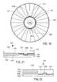
- the functional block 304is placed in the second substrate 300 ( FIG. 3 ) using a Fluidic Self-Assembly (FSA) process.
- FSAFluidic Self-Assembly
- the second substrate 300includes a receptor 302 configured to receive the functional block 304 .
- the receptor 302may be a recessed region formed into the second substrate 300 .
- the functional block 304has the trapezoidal shape
- the receptor 302has a similar shape and/or size so that the block 304 can be deposited therein.
- the receptor 302thus is configured with a complimentary shape for the particular shape of the functional block 304 in one embodiment.
- the functional block 304may be pressed, recessed, or otherwise placed onto the substrate using suitable methods.
- the substrate 300thus needs not have the receptor 302 formed so that the block 304 can be deposited therein. Instead, the block 304 can be pressed into the substrate 300 .
- the functional block 304may be deposited into the receptor 302 by an FSA method described in U.S. Pat. No. 5,545,291 which is hereby incorporated by its reference in its entirety. In one embodiment, the functional block 304 is recessed within the second substrate 300 or placed below or at a surface 300 -S of the second substrate 300 .
- the FSA processmay be performed with a web material in which a web material for the second substrate 300 is provided.
- the webmay contain a plurality of receptors 302 .
- the web materialis advanced through a web process apparatus.
- a slurry solutione.g., an FSA slurry
- the blocks 304would then fall into receptors 302 formed on the web material.
- the web materialcan then be sliced, singulated, separated so to form a plurality of substrates 300 each comprising one or more functional blocks 304 .
- the functional block 304includes one or more contact pads 306 so that conductive elements can be connected to the functional block 304 . Multiple contact pads may be included so that the functional block 304 can be coupled to more that one antennas or other devices.
- the contact pads 306can be formed on top of the functional block 304 .
- a conductive layer 308is connected to the contact pads 306 .
- an insulation layersuch as a planarization layer may be included on top of the functional block 304 that has been deposited in the receptor 302 . The insulation layer may provide a flat surface to the second substrate 300 as well as insulate certain components on top of the functional block 304 .
- the insulation layermay include one to more vias (not shown) created therethrough. Electrical interconnection to the contact pads 306 would be established through the vias. Forming the insulation layer and the vias are well known in the art and can be done by methods including laser drilling or photolithographic etching.
- the conductive layer 308can be formed of a suitable conductors and can include metallic films, conductive polymers, or inks filled with conductive particles. The conductive layer 308 can be formed by a method such as a subtractive process (using etching/lithography or laser ablation) on a metal film, or an additive process (such as printing) metal traces.
- the conductive layer 308is a conductive trace that extends from the functional block 304 .
- the contact pads 306may be extended so that it also forms the conductive layer 308 .
- the contact pads 306may also be integral parts of the conductive layer 308 .
- the conductive layer 308acts to enhance resonance for the RFID transponder or acts as a resonator for the RFID transponder.
- FIG. 4illustrates an embodiment where the integrated circuit chip 208 is incorporated into a second substrate 400 and recessed below a surface 400 -S of the substrate 400 .
- the structure in FIG. 4is similar to and is made similarly to the structure in FIG. 3 in all aspects except that the structure in FIG. 4 shows a functional block 404 recessed below the surface 400 -S.
- the second substrate 400includes a receptor 402 having the functional block 404 deposited therein as previously described.
- the functional block 404includes contact pads 406 formed on a surface 404 -T of the block 404 , in one embodiment.
- a conductive layer 408is coupled to the contact pads 406 such that electrical interconnection can be established to the functional block 404 .
- the conductive layer 408is a conductive trace that extends from the functional block 404 .
- the contact pads 406may be extended so that it also forms the conductive layer 408 .
- the contact pads 406may also be integral parts of the conductive layer 408 .
- the conductive layer 408acts to enhance resonance for the RFID transponder or acts as a resonator for the RFID transponder.
- an insulation layersuch as a planarization layer may be included on top of the functional block 404 that has been deposited in the receptor 402 .
- the insulation layermay provide a flat surface to the second substrate 400 as well as insulate certain components on top of the functional block 404 .
- the insulation layeris particularly helpful to provide a flat and even surface since the functional block 404 is recessed below the surface 400 -S of the second substrate 400 .
- the insulation layermay include one to more vias (not shown) created therethrough. Electrical interconnection to the contact pads 406 would be established through the vias.
- a metalization layersuch as the metalization layer 202 may be formed on a non-conductive or insulation layer.
- FIG. 5illustrates such an embodiment.
- a device 501 similar to the device 201includes a non-conductive layer 512 on a substrate 500 upon which a metalization layer 502 is formed.
- the metalization layer 502is formed on the non-conductive layer 512 .
- the non-conductive layer 512may cover the entire surface of the substrate 500 , or not.
- the metalization layer 502is not formed over all of the surface of the substrate 500 or the non-conductive layer 512 such that a portion 506 having no metalization layer 502 is provided for the device 501 .
- a cap layer 504is provided and formed over the metalization layer 502 and may also be formed over the portion 506 .
- a label 514 providing visual information or display for the device 501may be included in the device 501 and is placed over the cap layer 504 and may also be placed over the portion 506 .
- An RFID integrated circuit chip 508 similar to previously describedmay be coupled to the device 501 as shown in FIG. 5 or as previously described.
- the integrated circuit chip 508includes a conductive layer 510 that has a portion that is in a non-physical contact with the metalization layer 502 .
- the RFID integrated circuit chip 508is placed in a close proximity but in a non-physical contact with the metalization layer 502 .
- the RFID integrated circuit chip 508is placed in the portion 506 that does not include any metalization layer 502 .
- a portion of the conductive layer 510may very well be placed in a physical contact with the metalization layer 502 .
- the RFID integrated circuit chip 508is capacitively coupled to the metalization layer 502 such that the metalization 502 acts as an antenna for an RFID transponder for the device 501 .
- the RFID integrated circuit chip 508may be deposited in a second substrate which is then adhered to the first substrate 500 as previously discussed.
- the conductive layer that is coupled to the RFID integrated circuit chipacts as a coupler for the transponder.
- the conductive layerprovides additional surface area for the RFID integrated circuit chip so that the metalization layer can capacitively or inductively couple to the RFID integrated circuit chip.
- the conductive layer for the RFID transpondermay have any configuration.
- the conductive layermay also act as a resonator for the RFID transponder.
- the conductive layermay be of a straight, curved, circular, loop, dipole structure, folded, or folded-dipole structure, for examples.
- FIGS. 6-12illustrate a few of the exemplary configurations for the conductive layers (e.g., 210 , 308 , 408 , and 510 ) that are coupled to, attached to, or formed on the RFID integrated circuit chip.
- FIG. 6illustrates a conductive layer 602 having a loop configuration or circular configuration.
- the conductive layer 602is coupled to contact pads 606 that are formed on an RFID integrated circuit chip 604 .
- the RFID integrated circuit chip 604is deposited in a receptor 622 that is formed on a substrate 600 .
- the conductive layer 602is formed on a surface 600 -S of the substrate 600 and connected to the RFID integrated circuit chip 604 through the contact pads 606 .
- the substrate 600 having the RFID integrated circuit chip 602 deposited therein and the conductive layer 602 formed thereonis placed on a substrate portion of a device (such as portions 206 and 506 ).
- the substrate 600is placed on the portion that does not comprise a metal structure or a metalization layer as previously discussed.
- the conductive layer 602may be partially touching the metalization layer of the device but will have a portion that is not in physical contact with the metalization layer of the device.
- FIG. 7illustrates a conductive layer 702 with a curved configuration.
- FIG. 8illustrates a conductive layer 802 with a straight configuration.
- FIG. 9illustrates a conductive layer 902 with a dipole structure configuration.
- FIG. 10illustrates a conductive layer 1002 with a folded dipole configuration.
- FIG. 11illustrates a conductive layer 1102 with a curved dipole configuration.
- FIG. 12illustrates a conductive layer 1202 with another example of a curved dipole configuration. It will be apparent to those skilled in the art that other structures for the conductive layer might be possible.
- FIGS. 13-14illustrate an exemplary embodiment where an RFID transponder 1306 is directly incorporated into an electronic device such as a CD 1300 .
- the CD 1300includes a center portion 1302 with no conductive material or no metalization layer.
- the CD 1300also includes an opening 1304 .
- FIG. 14illustrates a cross section of the CD 1300 which includes a substrate 1320 which may be made of a plastic material. On the substrate 1320 , a metalization layer 1322 is formed.
- the metalization layer 1322is coded with information stored on the CD 1300 using methods known in the art.
- the CD 1300also includes a cap layer 1324 covering at least all of the metalization layer 1322 .
- the metalization layer 1322is not formed over the center portion 1302 of the CD 1300 .
- the RFID transponder 1306can be formed as previously described.
- the RFID transponder 1306includes a second substrate having an RFID IC chip 1308 deposited therein as previously described.
- the RFID transponder 1306is placed mostly on the center portion 1302 .
- the RFID transponder 1306may be placed near the edge of the center portion 1302 as shown in FIG. 13 .
- the RFID transponder 1306can be adhered to the center portion 1302 using adhesive. Other techniques of coupling the RFID transponder 1306 to the CD 1300 might be possible.
- the RFID transponder 1306is placed so that the RFID IC chip 1308 is not placed over any part of the CD 1300 that comprises the metalization layer 1322 .
- Portion of the second substrate of the RFID transponder 1306can touch or can be in a physical contact or overlap with a part of the CD 1300 that comprises the metalization layer 1322 without affecting the function of the RFID transponder 1306 so long as the RFID IC chip 1308 is not physically contacting the metalization layer 1322 .
- the RFID IC chip 1308is only capacitively coupled to the metalization layer 1322 of the CD 1300 .
- the RFID transponder 1306utilizes the metalization layer 1322 of the CD 1300 as an antenna for the RFID transponder 1306 .
- the CD 1300is balanced with one or more weight balancing components 1340 .
- the weight balancing components 1340may be structures that have similar weights as the RFID transponder 1306 .
- the weight of the weight balancing components 1340though need not match the weight of the RFID transponder 1306 for the CD 1300 to be well balanced.
- the weight balancing components 1340may be placed along the center portion 1302 in a predetermined fashion so as to achieve balance spinning weight for the CD 1300 .
- the RFID IC chip 1308may be created so small and/or thin that balancing may not be necessary.
- a labelmay be placed over the entire surface of the CD 1300 after the RFID transponder 1306 is incorporated into the CD 1300 .
- the labelmay cover all areas of the CD 1300 except for the opening 1304 .
- a label for a device such as the CD 1300is well known in the art.
- the labelmay be the layer that includes the desired weight balancing components 1340 such that when the label is placed over the CD 1300 , the weight would be balanced.
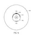
- FIG. 15illustrates another exemplary embodiment where an RFID transponder 1306 is incorporated into an electronic device such as a CD 1300 .
- the RFID transponder 1306includes a conductive layer 1310 which acts as a coupler or coupling extension for the RFID transponder 1306 that provides an extension for the RFID transponder IC chip 1308 so that the RFID IC chip 1308 can be capacitively coupled to the metalization layer 1322 of the CD 1300 .
- the conductive layer 1310can be formed on the second substrate of the RFID transponder 1306 as previously described.
- the conductive layer 1310can be formed or molded into the CD 1300 along an area of the center portion 1302 .
- the conductive layer 1310is electrical interconnected to the RFID IC chip 1308 .
- the RFID IC chip 1308may include contact pads (not shown) such that when the RFID transponder 1306 is coupled or embedded into the CD 1300 , the conductive layer 1310 will be in a physical contact with the contact pads.
- the conductive layer 1310is placed on the CD 1300 such that at least a portion of the conductive layer 1310 is not in a physical contact with the metalization layer.
- the CD 1300is balanced with one or more weight balancing components 1340 .
- the weight balancing components 1340may be placed along the center portion 1302 in a predetermined fashion so as to achieve balance spinning weight for the CD 1300 .
- a label, not shownmay be also placed over the entire surface of the CD 1300 after the RFID transponder 1306 is incorporated into the CD 1300 and the conductive layer 1310 establishing the contact with the RFID IC chip 1308 .
- the labelmay cover all areas of the CD 1300 except for the opening 1304 .
- the labelmay also include the weight balancing components 1340 as previously discussed.
- FIG. 16illustrates another exemplary embodiment where an RFID transponder 1306 is incorporated into an electronic device such as a CD 1300 .
- the embodiment in FIG. 16is similar to the embodiment show in FIG. 13 or 15 above in all aspects.
- the RFID transponder 1306includes a conductive layer 1310 which acts as a coupler for the RFID transponder 1306 that provides an extension for the RFID transponder IC chip 1308 so that the RFID IC chip 1308 can easily be capacitively coupled to the metalization layer 1322 of the CD 1300 .
- the conductive layer 1310 shown in FIG. 16has a straight configuration and includes an area that is in physical contact with a portion of the CD that comprises the metalization layer 1322 .
- the conductive layer 1310has a portion that is not in a physical contact with the metalization layer.
- the conductive layer 1310can be formed on the second substrate of the RFID transponder 1306 as previously described.
- the RFID IC chip 1308includes contact pads 1312 that interconnect to the conductive layer 1310 .
- the CD 1300is balanced with one or more weight balancing components 1340 which may be placed in locations that will balance the weight for the CD 1300 .
- a label, not shownmay be also placed over the entire surface of the CD 1300 after the RFID transponder 1306 is incorporated into the CD 1300 and the conductive layer 1310 establishing the contact with the RFID IC chip 1308 .
- the labelmay cover all areas of the CD 1300 except for the opening 1304 .
- the labelmay also include the weight balancing components 1340 as previously discussed.
- FIG. 17illustrates another exemplary embodiment where an RFID transponder 1306 is incorporated into an electronic device such as a CD 1300 .
- the embodiment in FIG. 17is similar to the embodiment show in FIG. 13 , 15 , or 16 above in all aspects.
- the RFID transponder 1306includes a conductive layer 1310 which acts as a coupler for the RFID transponder 1306 that provides an extension for the RFID transponder IC chip 1308 so that the RFID IC chip 1308 can easily be capacitively coupled to the metalization layer 1322 of the CD 1300 .
- the conductive layer 1310 shown in FIG. 17has a dipole and loop configuration and includes an area that is in physical contact with a portion of the CD that comprises the metalization layer 1322 .
- the conductive layer 1310has a portion that is not in a physical contact with the metalization layer.
- the conductive layer 1310can be formed on the second substrate of the RFID transponder 1306 as previously described.
- the CD 1300is balanced with one or more weight balancing components 1340 which may be placed in locations that will balance the weight for the CD 1300 .
- a label, not shownmay be also placed over the entire surface of the CD 1300 after the RFID transponder 1306 is incorporated into the CD 1300 and the conductive layer 1310 establishing the contact with the RFID IC chip 1308 .
- the labelmay cover all areas of the CD 1300 except for the opening 1304 .
- the labelmay also include the weight balancing components 1340 as previously discussed.
- FIG. 18illustrates an exemplary embodiment where an RFID transponder 1316 is incorporated directly into an electronic device such as a CD 1300 .
- the CD 1300includes a center portion 1302 with no conductive material or no metalization layer.
- the RFID transponder 1316is formed on the center portion 1302 .
- the CD 1300also includes an opening 1304 .
- FIG. 14illustrates a cross section of the CD 1300 which includes a substrate 1320 which may be made of a plastic material. On the substrate 1320 , a metalization layer 1322 is formed.
- the metalization layer 1322is coded with information stored on the CD 1300 using methods known in the art.
- the CD 1300also includes a cap layer 1324 covering at least all of the metalization layer 1322 .
- the metalization layer 1322is not formed over the center portion 1302 of the CD 1300 .
- an RFID IC chip 1308is molded, embedded, placed, coupled, or otherwise adhered to the center portion 1302 .
- Adhesivemay be used to coupled the RFID IC chip 1308 to the center portion 1302 .
- Other techniques of coupling the RFID IC chip 1308 to the CD 1300might be possible.
- the RFID IC chip 1308is not placed over any part of the CD 1300 that comprises the metalization layer 1322 .
- the RFID IC chip 1308is placed at a predetermined distance (e.g., between about 0.3 mm) away from the area that comprises the metalization layer 1322 .
- a conductive layer 1310is interconnected to the RFID IC chip 1308 , in one embodiment, connected to contact pads (not shown) formed on the RFID IC chip 1308 .
- the conductive layer 1310is formed directly on the center portion 1302 .
- the conductive layer 1310may be embedded, placed, coupled, or otherwise adhered to the center portion 1302 . At least some portions of the conductive layer 1310 are not in a physical contact with or overlap with a part of the CD 1300 that comprises the metalization layer 1322 .
- the RFID IC chip 1308is only capacitively coupled to the metalization layer 1322 of the CD 1300 via the conductive layer 1310 .
- the RFID transponder 1316utilizes the metalization layer 1322 of the CD 1300 as the antenna for the RFID transponder 1316 .
- the CD 1300is balanced with one or more weight balancing components 1340 .
- the weight balancing components 1340may be placed along the center portion 1302 in a predetermined fashion so as to achieve balance spinning weight for the CD 1300 .
- a labelnot shown may be placed over the entire surface of the CD 1300 after the RFID transponder 1316 is formed on the CD 1300 .
- the labelmay cover all areas of the CD 1300 except for the opening 1304 .
- the labelmay also include the weight balancing components 1340 as previously mentioned.
- FIGS. 19-20illustrate an exemplary embodiment where an RFID transponder 1306 is directly incorporated into an electronic device such as a CD 1300 .
- the CD 1300includes a center portion 1302 with no conductive material or no metalization layer.
- the CD 1300also includes an opening 1304 .
- FIG. 20illustrates a cross section of the CD 1300 which includes a substrate 1320 which may be made of a plastic material.
- a non-conductive layer 1344is provided on the substrate 1320 .
- a metalization layer 1322is formed on the substrate 1320 (or on the non-conductive layer 1344 ).
- the metalization layer 1322is coded with information stored on the CD 1300 using methods known in the art.
- the CD 1300also includes a cap layer 1324 covering at least all of the metalization layer 1322 .
- the metalization layer 1322is not formed over the center portion 1302 of the CD 1300 .
- an RFID transponder 1306is formed on or included into a label 1330 of the CD 1300 ( FIG. 20 ).
- an RFID IC chip 1308is embedded into the label 1330 using methods known in the art (e.g., FSA).
- the chip 1308may also be placed into the label 1330 using other methods.
- the label 1330may be a second substrate as previously described and include a receptor configured to receive the chip 1308 .
- the chip 1308may also be adhered to the label 1330 using a convenient technique such as using adhesive.
- a conductive layer 1310is then formed on the label 1130 and interconnected to the chip 1308 .
- the chip 1308may include contact pads (not shown) that the conductive layer 1310 is connected to.
- a planarization layermay be placed over the side label 1330 to provide a smooth surface and a protective layer for the chip 1308 .
- the conductive layer 1310is formed on the CD 1300 and is connected to the chip 1308 when the label 1330 is placed over the CD 1300 .
- the label 1330is then placed over the CD 1300 .
- the label 1330has a portion 1331 that overlaps with the center portion 1302 when the label 1330 is placed over the CD 1300 .
- the chip 1308 and portions of the conductive layer 1310is formed in the portion 1331 such that when the label 1330 is placed over the CD 1300 , the chip 1308 is not in a physical contact with a part of the CD that comprises the metalization layer 1322 .
- the conductive layer 1310when the label 1330 is placed over the CD 1300 , a portion of the conductive layer 1310 is also not in a physical contact with the part of the CD that comprises the metalization layer 1322 .
- the conductive layer 1310has a circular configuration and does not have a part that overlaps the part of the CD that comprises the metalization layer 1322 .
- the RFID transponder 1306forms a capacitive coupling to the metalization layer 1322 utilizing the metalization layer 1322 as an antenna layer.
- the RFID transponder 1306can be formed as previously described and then laminated or otherwise coupled to the label 1330 ( FIG. 21 ).
- the RFID transponder 1306includes a second substrate 1380 having an RFID IC chip 1308 deposited therein.
- the RFID transponder 1306also includes a conductive layer 1310 formed on the second substrate 1380 .
- the second substrate 1380 with all the necessary componentsis then laminated or adhered to the label 1330 as shown in FIG. 21 .
- the label 1330is then placed over the CD 1300 .
- the label 1330has a portion 1331 that overlaps with the center portion 1302 when the label 1330 is placed over the CD 1300 .
- the REID transponder 1306is laminated or adhered to the portion 1331 such that when the label 1330 is placed over the CD 1300 , the chip 1308 is not in a physical contact with a part of the CD that comprises the metalization layer 1322 . Additionally, when the label 1330 is placed over the CD 1300 , a portion of the conductive layer 1310 is also not in a physical contact with the part of the CD that comprises the metalization layer 1322 . In one embodiment, the conductive layer 1310 has a circular configuration and does not have a part that overlaps the part of the CD that comprises the metalization layer 1322 .
- the RFID transponder 1306forms a capacitive coupling to the metalization layer 1322 utilizing the metalization layer 1322 as an antenna layer.
- the CD 1300is balanced with one or more weight balancing components 1340 as previously mentioned.
- the weight balancing components 1340may be placed on the label 1330 , for example, along the portion 1331 of the label 1330 .
- the weight balancing components 1340may be placed along the center portion 1302 in a predetermined fashion so as to achieve balance spinning weight for the CD 1300 after the label 1300 is affixed thereto.
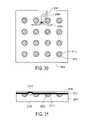
- FIGS. 22-23illustrate an exemplary embodiment where an RFID transponder 1366 is incorporated into an electronic device such as a CD 1300 .
- the CD 1300includes a center portion 1302 with no conductive material or no metalization layer.
- the CD 1300also includes an opening 1304 .
- FIG. 4illustrates a cross section of the CD 1300 which includes a substrate 1320 which may be made of a plastic material. On the substrate 1320 , a metalization layer 1322 is formed.
- the metalization layer 1322is coded with information stored on the CD 1300 using methods known in the art.
- the CD 1300also includes a cap layer 1324 covering at least all of the metalization layer 1322 .
- the metalization layer 1322is not formed over the center portion 1302 of the CD 1300 .
- an RFID transponder 1366includes a center ring structure or substrate 1350 which is placed on the center portion 1302 of the CD 1300 .
- the center ring structure 1350includes an RFID IC chip 1305 incorporated therein.
- the RFID IC chip 1308is embedded into the center ring structure 1350 using methods known in the art (e.g., FSA).
- the chip 1308may also be placed into the center ring structure 1350 using other methods.
- the center ring structure 1350is a second substrate that is adhered, coupled, or otherwise attached to the substrate 1320 of the CD 1300 at the center portion 1302 .
- the center ring structure 1350includes a receptor (not labeled) that may be configured to receive the chip 1308 .
- the chip 1308may also be adhered to the center ring structure 1350 using a convenient technique such as using adhesive.
- a conductive layer 1310is then formed on the center ring structure 1350 and interconnected to and extended from the chip 1308 .
- the chip 1308may include contact pads (not labeled) that the conductive layer 1310 is connected to.
- the center ring structure 1350is placed over the CD 1300 at the center portion 1302 .
- the center ring structure 1350may cover the entire center portion 1302 or may only cover a portion of the center portion 13002 .
- the center ring structure 1350is placed on the CD 1300 such that the chip 1308 and portions of the conductive layer 1310 are not in physical contacts with a part of the CD that comprises the metalization layer 1322 .
- the conductive layer 1310has a circular configuration and does not have a part that overlaps the part of the CD that comprises the metalization layer 1322 .
- the RFID transponder 1366forms a capacitive coupling to the metalization layer 1322 utilizing the metalization layer 1322 as an antenna layer.
- the RFID transponder 1366includes one or more weight balancing components 1340 similar to previous embodiments ( FIGS. 22-23 ).
- the weight balancing components 1340may be placed or embedded directly into the center ring structure 1350 .
- the weight balancing components 1340may be placed along the center portion 1302 in a predetermined fashion so as to achieve a balance spinning weight for the CD 1300 after the RFID transponder 1366 is affixed thereto.
- a labelmay be placed over the entire surface of the CD 1300 after the RFID transponder 1366 is incorporated into the CD 1300 .
- the labelmay cover all areas of the CD 1300 except for the opening 1304 .
- FIG. 24illustrates an exemplary method 2300 of processing an electronic device in accordance to embodiments of the present invention.
- the electronic devicemay be a CD 1300 or other electronic device such as a CD, CD-ROM, CD-R, CD-RW, CD-I, DVD, DVD-ROM, DVD-R, and DVD-RAM.
- Processing the deviceincludes tagging which may include, but is not limited to identifying, authenticating, recognizing, inventorying, checking-in, checking-out, tracking, locating, and sensing the electronic device.
- taggingis achieved using an RFID system comprises using an RFID reader and an RFID transponder made in accordance to embodiments of the present invention.
- an electronic device with identification information for the electronic deviceis provided.
- the electronic devicecomprises a first substrate having a metalization layer formed on the substrate, a cap layer covering at least all of the metalization layer and at least a portion of the substrate is not covered by the metalization layer.
- an RFID transponderaccording to embodiments of the present invention is obtained.
- the RFID transponderis incorporated into the device as previously described.
- the RFID tagincludes an RFID circuit chip that is capacitively coupled to the metalization layer thus creating the RFID transponder.
- an RFID reader receptive of the RFID transponderis provided.
- the RFID transpondercomprises the identification information and is incorporated into the electronic device.
- a method similar to method 2300is provided.
- the integrated circuit chipis capacitively coupled to the metalization layer through the conductive layer and the metalization layer.
- a method similar to method 2300is provided.
- the integrated circuit chipis placed in proximity and in non-physical contact with the metalization layer.
- the conductive layerhas at least a portion placed in a non-physical contact with the metalization layer.
- the integrated circuit chipis capacitively coupled to the metalization layer through the conductive layer and the metalization layer.
- a method similar to method 2300is provided.
- the center ring substratecomprises an integrated circuit chip disposed therein.
- a conductive layeris attached to the integrated circuit chip.
- One or more weight balancing componentsare deposited on the center ring substrate.
- the integrated circuit chipis placed such that the integrated circuit chip is in proximity and in non-physical contact with the metalization layer.
- the conductive layerhas at least a portion placed in a non-physical contact with the metalization layer.
- the integrated circuit chipis capacitively coupled to the metalization layer through the conductive layer and the metalization layer.
- an electronic devicesuch as a CD or DVD is tagged using an RFID transponder that is incorporated directly into the electronic device in accordance to exemplary embodiments of the present invention.
- a CD or DVDis tagged using such RFID transponder.
- a devicesuch as a CD or DVD that is tagged using an RFID transponder that is incorporated directly into the electronic device is checked in or out of a library using a complimentary RFID reader, wherein the RFID transponder includes information or identification information about the device and communicates/transmits the information the RFID reader, which identifies the information accordingly and facilitates the checking in and/or checking out of the item.
- the RFID readerpicks up the information from the RFID transponder incorporated on the device and automatically identifies and facilitates the check in process of the device at the library.
- the RFID transponderfunctions as a security device for an electronic device that incorporates the RFID transponder directly into the electronic device.
- the RFID transpondersends a signal to a security gate which includes an RFID reader and is positioned at a particular location as the device passes through the gate.
- the RFID transponderallows the device to be detected and/or checked out.
- Such security gatemay be included at a retailer selling the device, a rental store renting the device, or a library maintaining the device.
- the RFID transponderenables automatic check in and/or check out of an electronic device that incorporates the RFID transponder directly into the electronic device.
- the device with the RFID transpondercan be automatically detected for checking in and checking out process.
- the RFID transponderfacilitates sorting of a device returned to a particular location such as a library or a rental store.
- a devicereturned to a particular location such as a library or a rental store.
- an electronic deviceincludes an RFID transponder that is incorporated directly into the device, when the device is return to appropriate location where an RFID reader is placed, the item is detected and automatically checked in.
- an RFID-enable automatic sorteris provided. The RFID-enable automatic sorter picks up signal from the RFID transponder on the device, automatically checks in the device, and automatically sorts and/or places the device into an appropriate location/container according to the information provided in the RFID transponder.
- the RFID transponderfacilitates shelving, organizing, locating, identifying, or tracking, or other similar task an electronic device that incorporates the RFID transponder directly into the electronic device.
- An RFID readeris provided. The RFID reader can scan or pick up signals from the device's RFID transponder and enters or checks the location of the device which facilitates shelving, organizing, locating, identifying, tracking, or other similar task of the device.
- an RFID ICmay be integrated with a device such as a CD or DVD and may, (in addition to or an alternative to identifying, through a contactless, wireless manner, the particular CD or the content on the CD) provide a way to prevent successful copying of the CD, DVD, or other machine readable medium.
- the RFID ICis embedded within the CD itself and may be read by a reader in the CD player.
- the RFID ICmay transmit a code (which may be encoded or encrypted) to the reader in the CD player (or within the system which includes the CD player), and the CD player can process this code to determine whether the CD is authentic (and not a pirated copy).
- a codewhich may be encoded or encrypted
- One implementationmay merely involve wireless by reading a code or value from the RFID IC when the machine readable medium (which contains the RFID IC) is placed into a playback device (e.g., a CD player) and comparing this code or value to a code or value read from the machine readable medium. If the codes or values match, then the playback device “knows” that the machine readable medium is authentic. If the codes or values do not match, then the playback device “knows” that the machine readable medium is NOT authentic and the playback device will refuse to playback (or otherwise interact with) the medium and may cause the medium to be ejected.
- a playback devicee.g., a CD player
- the playback devicewould normally include a standard playback device (e.g., a CD laser and head and associated electronics and motors) and an RFID reader which transmits an interrogation signal to the RFID IC in the machine readable medium and which receives a response from the transponding RFID IC which is embedded with the machine readable medium which is inserted into the playback device.
- a standard playback devicee.g., a CD laser and head and associated electronics and motors
- an RFID readerwhich transmits an interrogation signal to the RFID IC in the machine readable medium and which receives a response from the transponding RFID IC which is embedded with the machine readable medium which is inserted into the playback device.
- FIG. 25shows an example of a playback system for use in one exemplary aspect of the invention.
- the playback system 2501may be a stand-alone CD player or DVD player or may be part of a larger system (e.g., the playback system 2501 may be a CD/DVD drive in a general purpose computer system).
- the playback system 2501is designed to receive a machine readable medium 2503 (which may be a CD, DVD, etc.) which includes an RFID IC 2502 .
- the RFID IC 2502includes one or more codes or values which identify the medium and which can also be used to prevent successful copying of the content stored on the medium.
- a drive system 2505receives the medium 2503 and positions the medium 2503 relative to a read head (e.g., a CD laser and detector head).
- the drive system 2505is coupled to and controlled by the control logic 2509 .
- the control logic 2509controls the drive system 2505 and also controls the operation of and receives signals (e.g., codes or values) from the RFID reader 2507 . These signals are obtained from the RFID IC.
- the Input/Output (“I/O”) control 2511is coupled to the control logic 2509 in order to provide an output and/or input to the playback system 2501 .
- the I/O control 2511may receive audio or audiovisual data from the medium 2503 and provide this data to speakers or a display device or to another subsystem (e.g., portions of a computer or TV).
- the control logic 2509may perform the comparisons described above (e.g., matching a code from the RFID IC with a code stored in the medium 2503 ) in order to verify that the medium is authentic.
- Other alternative playback architecturesmay be implemented with an RFID reader which reads an RFID IC embedded with a machine readable medium.
- Another exemplary implementationmay, rather than merely determining whether a value read from the RFID IC matches a value read from the machine readable medium which contains the RFID IC, use an encoding scheme or encryption scheme to make copying difficult.
- One or more values stored in the RFID ICmay be encoded and/or encrypted and one or more values stored on the machine readable medium may also be encoded and/or encrypted, and the playback device processes these values to determine whether the content of the machine readable medium is authentic. For example, if each CD or other medium from a particular source (e.g., Microsoft) has a serial number, that serial number may be encrypted (e.g., with a private key of a public key/private key system) and stored in the RFID IC.
- a particular sourcee.g., Microsoft
- the playback deviceWhen the playback device reads the RFID IC, it retrieves this encrypted serial number and decrypts this number (e.g., with the source's public key) to obtain the unencrypted (“clear”) serial number and compares this serial number from the RFID IC to the serial number stored on the medium. If there is a match then the medium is authentic and if there is no match then it is not authentic. Numerous other encoding schemes or encryption schemes which are known in the art may alternatively be applied.
- an RFID transponderis incorporated into an item that may include or otherwise allow a conductive layer or a metalization layer to be attached to the item.
- the conductive layer for this itemmay not necessarily perform any electronic function such as the metalization layer for a CD disc previously discussed.
- the conductive layer for this itemmay function as a tampered proof, protective, cover, a sealing, or an identification layer or label for an item or a packaging of an item.
- the conductive layeritself may be physically altered or configured so that the conductive layer can act as a part of an antenna and/or a resonance structure for an RFID transponder. With such physical alteration, the conductive layer can then have an additional function, to act as a part of an antenna and/or a resonance structure for the RFID transponder.
- An RFID integrated circuit chipis interconnected to the conductive layer to form an RFID transponder. The item with such RFID transponder included can then be tagged, authenticated, tracked, or the like using an RFID system as previously described.
- These embodimentsare particularly useful to incorporate an RFID system into a pharmaceutical item, a Blister Pack, a medicine bottle, a food item, a bottle, or any other merchandise that may currently include a conductive layer such as a foil layer in its packaging.
- tamper-proof packagingthat includes a foil layer or other conductive material.
- Such itemsinclude medicine, personal product (e.g., toothpaste, mouthwash, cosmetic product), food, wine, cellular/wireless device, memory card, electronic device, etc.
- personal producte.g., toothpaste, mouthwash, cosmetic product
- foode.g., wine, cellular/wireless device, memory card, electronic device, etc.
- a foil sealingover an opening of a bottle or a tube that contains a product wherein breakage in the sealing would indicate that the product has been opened, used, tested, or otherwise tampered with.
- Blister Pack or a Blister Pack like packagingthat include a metallic or a foil layer.
- these types of packaging or sealingalso allow for displays of the item or product contained within the packages as well as providing security or authenticity of the item, theft resistant or indicator for the item, and/or tamper-proof packaging for the item.
- FIG. 26illustrates a typical blister pack 1000 that includes a thermoformed “blister” or tray 1002 which houses an item or product or a plurality of such item or product 1004 .
- a “blister card” or cover 1006which may be a printed card with an adhesive coating, is adhered on the front surface of the tray 1002 .
- the blister/tray 1002is attached to the blister card/cover 1006 using a machine that may also be used to package the product between the tray and the cover.
- the blister packcan be as small or as large as desired for the particular product.
- the blister packtypically includes a foil layer, which could be the cover 1006 in many instances.
- this foil layeris made to include one or more slots and an RFID integrated circuit chip placed over a portion of the slot (see below, FIGS. 28-31 ).
- the foil layerfunctions as a part of an antenna and/or resonator and together with the RFID integrated circuit chip functions as an RFID transponder.
- FIG. 27illustrates a medicine bottle 2000 that may include a tampered proof foil layer 2002 .
- the bottle 2000typically stores a particular medicine.
- a sealing coversuch as the foil layer 2004 is placed over the mouth or opening of the bottle 2000 .
- a cap/cover 2006is also typically placed over the bottle 2000 .
- this foil layer 2004can be made to include one or more slots and an RFID integrated circuit chip placed over a portion of the slot (see below, FIGS. 32-33 ).
- the foil layerfunctions as a part of an antenna and/or resonator and together with the RFID integrated circuit chip functions as an RFID transponder. Similar implementations can be applied to other items such as food, cosmetic products, or personal products.
- FIG. 28illustrates an exemplary embodiment of a conductive layer 2804 (e.g., a foil layer) that is configured so that it can function as a part of an antenna structure for an RFID device 2800 . Additionally, the conductive layer 2804 can also be configured to be a part of or a resonator for the RFID device 2800 .
- the RFID device 2800(also referred to as an RFID tag or transponder) comprises a substrate 2802 upon which the conductive layer 2804 is formed.
- the conductive layer 2804includes an opening line or slot 2812 .
- the opening line 2812is typically a slot cut through a portion of the conductive layer 2804 .
- the slot 2812transforms the conductive layer 2804 into a part of an antenna structure that can be used for an RFID system.
- the opening line 2812can be etched, laser cut, or otherwise formed into the conductive layer 2804 using methods known in the art.
- the opening line 2812can also function as a separator that creates two sides for the conductive layer 2804 so that the conductive layer 2804 can function as a part of an antenna and can be coupled to a circuit component without shorting out.
- the opening line 2812also allows the conductive layer 2804 to be configured like a loop or two-plates antenna. In one embodiment, the opening line 2812 has a width of about 0.5-5 mm.
- an additional opening line 2813is formed in the conductive layer 2804 .
- the additional opening line 2813can extend from the opening line 2812 or can intersect with the opening line 2812 as illustrated in FIG. 28 .
- the additional opening line 2813functions as a resonator for the RFID tag 2800 .
- the length of the opening line 2813corresponds to a particular frequency that the RFID tag 2800 is to be operated in. For instance, for an operating frequency of about 800-950 MHz, the opening line 2813 may have a length of about 1-1.5 inches.
- the length of the opening line 2813is inversely proportional to the operating frequency level for the RFID tag 2800 . In another example, for an operating frequency of about 2-3 GHz, the opening line 2813 may have a length of about 0.2-0.5 inches.
- the RFID integrated circuit chip 2808is placed, deposited, or recessed in a strap substrate 2808 ( FIG. 29 ) prior to being interconnected to the conductive layer 2804 .
- the strap substrate 2808is provided.
- the strap substrate 2808may include a receptor (not labeled) configured to receive the RFID integrated circuit chip 2808 in the form of a block that include the necessary circuit or electrical component formed thereon (similar to previously discussed with reference to FIGS. 3-4 ).
- the RFID integrated circuit chip 2808may be deposited into the receptor using FSA as previously discussed ( FIG. 29 ).
- the RFID integrated circuit chip 2808is recessed into the strap substrate 2808 using other suitable methods or techniques.
- the RFID integrated circuit chip 2808may include one or more contact pads 2814 used to electrically interconnect the electrical component to the conductive layer 2804 . Additional contact pads may also be included for other purposes.
- the RFID integrated circuit chip 2808may include an interconnect feature 2816 to provide additional contact area for the RFID integrated circuit chip 2808 .
- the interconnect feature 2816may also increase or act as a resonator for the RFID tag that the RFID IC chip 2808 is included or coupled to.
- a protective layer or a cap layer 2806is placed over the substrate 2802 as illustrated in FIG. 28 .
- the protective layer 2806serves to prevent damages to the RFID integrated circuit chip 2808 as well as the conductive layer 2804 .
- the protective layer 2806can also function to serve as a sealing or a tamper-proof indicator since a slot or an opening is formed into the conductive layer 2804 .
- Adhesive layersmay be used to couple the substrate 2802 to the conductive layer 2804 and/or to couple the conductive layer 2804 to the protective layer 2086 . Additionally, adhesive may also be used to couple the RFID integrated circuit chip 2808 to the conductive layer 2804 as previously discussed. Other methods or mechanical coupling can also be used, e.g., soldering.
- FIGS. 30-31illustrate an exemplary embodiment of a pharmaceutical product that includes a Blister Pack with an RFID tag made in accordance to embodiments of the present invention.
- a conductive layer (or a foil layer) 3002is provided with a slot 3004 and a slot 3006 .
- An RFID integrated circuit chip 3008is placed over a portion of the slot 30046 .
- the conductive layer 3002is placed over a substrate 3014 .
- the substrate 3014is a tray with feature 3012 that is configured to house a medicine tablet or a plurality of medicine tablets 3010 .
- the tablets 3010are housed between the conductive layer 3002 and the substrate 3014 as shown in FIG. 31 .
- a protective layer 3016may also be placed over the conductive layer to protect the conductive layer 3002 and the RFID integrated circuit chip 3008 .
- the conductive layer 3002is the layer with the features 3012 that can receive the tablets 3010 .
- the conductive layer 3002is simply a label of the Blister Pack.
- FIGS. 32-33illustrates an exemplary embodiment of a conductive layer 2004 (e.g., a foil layer) that is altered so that it can function as a part of an antenna and/or a resonator structure and can accommodate and interconnect to an RFID integrated circuit chip 2018 for an RFID device 2001 .
- the RFID device 2001also functions as a protective sealing or a sealing cap for an item such as the medicine bottle 2000 shown in FIG. 27 .
- the bottle 2000includes a sealing layer that includes a conductive layer 2004 placed over the opening 2010 of the bottle 2000 .
- the bottle 2000may include a bottle neck 2008 as is typically known in the art.
- a substrate layer 2016is placed over the opening 2010 .
- a conductive layer (e.g., a foil layer) 2004is placed over the substrate 2016 .
- a slot 2012is created in the conductive layer 2004 .
- the slot 2012 created into the conductive layer 2004enables the conductive layer 2004 to be configured to be a part of an antenna structure for the RFID device 2001 .
- An RFID integrated circuit chip 2018is placed over the slot 2012 to interconnect the RFID integrated circuit chip 2018 to the conductive layer 2004 .
- Additional slotsuch as slot 2016 can also be included to add resonance to the RFID device 2001 .
- the length of the slot 2016corresponds to the desired frequency for the RFID device.
- the slot 2016has a length of about 1-1.5 inches which will enable the RFID device 2001 to operate in the range of about 800-950 MHz. In one embodiment, the slot 2016 has a length of about 0.2-0.5 inches which will enable the RFID device 2001 to operate in the range of about 2-3 GHz.
- the RFID integrated circuit chip 2018is recessed within a strap substrate 2014 as previously discussed. The strap substrate 2014 is then placed over the slot 2012 in a way that enable the RFID integrated circuit chip 2018 to interconnect to the conductive layer 2004 . In one embodiment, a protective layer 2020 is placed over the conductive layer 2004 and the RFID integrated circuit chip 2018 .
- the substrate 2060 , the conductive layer 2004 , the RFID integrated circuit chip 2018 (or the RFID integrated circuit chip 2018 recessed in the strap substrate 2014 ), and the protective layer 2020are assembled together and then placed over the opening 2010 of the bottle 2000 .
- the assembly with all the componentsthus acts as a tamper-proof sealing as well as an RFID tag for the bottle 2000 .
- the material or content within the bottle 2000can be authenticated, tagged, controlled, and/or protected using a conventional RFID system that works with the RFID tag installed on the bottle 2000 . Additionally, no new complicated processing step is needed to add to the assembling or packaging of the bottle 2000 to add an RFID feature to the bottle 2000 .
- FIG. 34illustrates an exemplary web process 7000 of assembling a packaging, such as a Blister Pack, that houses one or more items, such as a medicine tablet.
- the particular Blister Packis assembled to include an RFID transponder so that the Blister Pack can be a tamper-proof packaging for the medicine tablet as well as providing a tagging and authentication tool for the medicine tablet.
- a web processingis convenient for assembling the packaging for the item with the Blister Pack, other processing method can be used.
- material for an RFID strap substrate 7010is provided.
- the RFID strap substrate 7010is provided in a roll format.
- recesses 7011are created into the strap substrate 7010 using a tool 7003 , which could be a molding tool or an embossing device.
- Each recess 7011is configured to receive an RFID integrated circuit chip.
- Each recess 7011may have a shape complimentary to the shape of the RFID integrated circuit chip as previously discussed.
- the strap substrate 7010is advanced to location 7004 .
- an RFID integrated circuit chip 7012is deposited into the recess 7011 .
- the RFID integrated circuit chip 7012can be a shaped block or object that includes electronic component for the RFID integrated circuit chip 7012 .
- an FSA processis used to deposit the RFID integrated circuit chip 7012 into the recess 7011 .
- An inspection toolcan be provided at location 7006 .
- the strap substrate 7010can be inspected for recesses 7011 that are not filled or properly filled with the RFID integrated circuit chips 7012 .
- the RFID integrated circuit chips 7012can also be inspected for functionality and other necessary inspection.
- the webcan be singulated, separated, cut, or sliced to produce individual strap substrate 7010 that comprises the RFID integrated circuit chip 7012 deposited therein (RFID strap 7090 ).
- a Blister Pack substrate 7201is provided.
- the Blister Pack substrate 7201is provided in a roll format.
- recesses 7203are created into the Blister Pack substrate 7201 .
- the Blister Pack substrate 7207already includes recesses 7203 created therein.
- the Blister Pack substrate 7207includes designated areas 7203 reserved for items 7206 (e.g., medicine tablets) to be placed thereon.
- items 7206are placed on the Blister Pack substrate 7201 .
- a conductive layer 7208is placed over the Blister Pack substrate 7201 .
- an additional layermay be placed over the items before the conductive layer 7208 is placed over the Blister Pack substrate 7201 .
- the conductive layer 7208includes slots (not shown) created therein as previously discussed.
- individual RFID strap 7090 that comprises the RFID integrated circuit chip 7012 deposited thereinis placed over the conductive layer 7208 as previously discussed.
- the individual RFID strap 7090is placed over the conductive layer 7208 in a way that enable interconnection between the RFID integrated circuit chip 7012 and the conductive layer 7208 as previously discussed.
- the RFID integrated circuit chip 7012is placed over a portion of the slot that is formed in the conductive layer 7208 .
- a protective layer 7213is placed over the Blister Pack substrate 7201 .
- the Blister Pack substrate 7201is singulated into individual Blister Pack 7500 .
- Each Blister Pack 7500includes one or a plurality of items 7206 housed between the Blister Pack substrate 7201 and the conductive layer 7208 that includes the RFID integrated circuit chip 7012 attached thereto.
- the Blister Pack 7500 made in accordance to process 7000includes an RFID transponder that can work with a corresponding RFID reader. It is to be noted that other conventional step of making a Blister Pack may be added to the process 7000 .
- FIG. 35illustrates an exemplary web process 8000 of assembling a packaging, such as a medicine bottle, that houses one or more items, such as a medicine tablet.
- the particular bottleis assembled to include an RFID transponder so that the bottle can be a tamper-proof packaging for the medicine tablet as well as providing a tagging and authentication tool for the medicine tablet.
- a web processingis convenient for assembling the bottle, other processing method can be used.
- a conductive layer 8002is provided.
- an additional layer(not shown) may be coupled to the conductive layer 8002 .
- the conductive layer 8002is provided in a roll format.
- slotsare cut into the conductive layer 8002 .
- a cutting tool 8004is used to cut the slot.
- the slotenables the conductive layer 8002 to function as a part of an antenna structure for an RFID transponder/tag. Instead of cutting, an etching or laser cutting tool can also be used to create the slot in the conductive layer 8002 .
- an RFID strap 8006is placed over the conductive layer 8002 .
- the RFID strap 8006can be one that is created in the process 7000 as previously mentioned (RFID strap 7090 ).
- the RFID strap 8006thus includes an RFID integrated circuit chip recessed therein (for example, using FSA).
- the RFID strap 7090 processed at location 7001 - 7007 previously described in process 7000 ( FIG. 34 )is used for the RFID strap 8006 and coupled to the conductive layer 8002 at location 8005 ( FIG. 35 ).
- a protective layer 8008is placed over the conductive layer 8002 that now includes the RFID strap 8006 coupled thereto.
- the conductive layer 8002 with the RFID strap 8006 and protected by the protective layer 8008is placed over an item 8010 .
- the item 8010is a bottle such as the bottle 2000 previously discussed.
- the conductive layer 8002 with the RFID strap 8006 and protected by the protective layer 8008is placed over an opening of a bottle.
- a cap 8013is also placed over the bottle 8010 and a bottle 8012 is then formed.
- the bottle 8012thus has an RFID transponder incorporated into its sealing providing tagging, authenticating, and tamper-proofing capability for the bottle 8012 .
- FIG. 36illustrates an exemplary web process 9000 of assembling a packaging, such as a medicine bottle cap that is to be placed over a medicine bottle houses one or more items.
- the process 9000is similar to the process 8000 previous described ( FIG. 35 ) with the exception that a conductive layer with an RFID strap is placed within a cap that can be used for a bottle.
- the particular bottle that can be used with the cap from the process 9000can be conventionally packaged.
- the cap of the bottlewould be the component that includes the tagging information.
- the particular bottlemay include other necessary sealing or tamper proof sealing as is known in the art of as described in this document. It is to be noted that although a web processing is convenient for assembling the bottle, other processing method can be used.
- a conductive layer 9002is provided.
- an additional layer(not shown) may be coupled to the conductive layer 9002 .
- the conductive layer 9002is provided in a roll format.
- slotsare cut into the conductive layer 9002 .
- a cutting tool 9004is used to cut the slot.
- the slotenables the conductive layer 9002 to function as a part of an antenna structure for an RFID transponder/tag. Instead of cutting, an etching or laser cutting tool can also be used to create the slot in the conductive layer 9002 .
- an RFID strap 9006is placed over the conductive layer 9002 .
- the RFID strap 9006can be one that is created in the process 7000 as previously mentioned (RFID strap 7090 ).
- the RFID strap 9006thus includes an RFID integrated circuit chip recessed therein (for example, using FSA).
- the RFID strap substrate processed at location 7001 - 7007 previously described in process 7000 ( FIG. 34 )is used for the RFID strap substrate 9006 and coupled to the conductive layer 9002 at location 9005 ( FIG. 36 ).
- a protective layer 9008is placed over the conductive layer 9002 that now includes the RFID strap 9006 coupled thereto.
- the conductive layer 9002 with the RFID strap 9006 and protected by the protective layer 9008is placed over an item 9010 .
- the item 9010is a bottle cap. The bottle cap 9010 thus has an RFID transponder incorporated therein.
- an itemsuch as a medicine pack, a medicine bottle, a food item, a beverage item, or the like is tagged using an RFID transponder that is incorporated into the packing of the item in accordance to exemplary embodiments of the present invention.
- the RFID transponderis incorporated into the item utilizing a conductive layer that may be included in the packaging and an RFD integrated circuit chip as previously described.
- a complimentary RFID readeris provided to work with the RFID transponder.
- the RFID transponderincludes information or identification information about the item and communicates/transmits the information the RFID reader, which identifies the information accordingly and facilitates the tagging, authenticating, distributing, or the like of the item.
- the RFID transponderfunctions as a security device for an item that incorporates the RFID transponder as described.
- the RFID transpondersends a signal to a security gate which includes an RFID reader and is positioned at a particular location as the item passes through the gate.
- the RFID transponderallows the item to be detected and/or checked out.
- security gatemay be included at a retailer selling the device, a pharmacy, a drug store, a hospital, or other establishes that distribute or control the item.
- the RFID transponderfacilitates sorting and inventorying of an item that incorporates the RFID transponder as previously described.
- the RFID transponderfacilitates shelving, organizing, locating, identifying, or tracking, or other similar task an item that incorporates the RFID transponder as previously described.
- An RFID readeris provided. The RFID reader can scan or pick up signals from the item's RFID transponder and enters or checks the location of the device which facilitates shelving, organizing, locating, identifying, tracking, or other similar task of the item.
- an RFID ICmay be integrated with an item such as a pharmaceutical product and may, (in addition to or an alternative to identifying, through a contactless, wireless manner, the particular item) provide a way to prevent distribution of non-genuine product or replica of the item.
- the RFID ICis embedded within the packaging of the item (e.g., protective sealing). When the sealing is broken or otherwise tampered with, the item cannot be authenticated.
- protective sealingWhen the sealing is broken or otherwise tampered with, the item cannot be authenticated.
- One implementationmay merely involve wireless by reading or searching for a code or value from the RFID IC that is originally installed in the sealing. If the codes or values match and can be found in the item, then the item is authenticated. If the codes or values do not match, or simply does not exist in the sealing, then the item is not authenticated and a consumer can be alerted as to the authenticity of the item.
Landscapes
- Engineering & Computer Science (AREA)
- Physics & Mathematics (AREA)
- General Physics & Mathematics (AREA)
- Computer Hardware Design (AREA)
- Microelectronics & Electronic Packaging (AREA)
- Computer Security & Cryptography (AREA)
- Automation & Control Theory (AREA)
- Electromagnetism (AREA)
- Theoretical Computer Science (AREA)
- Power Engineering (AREA)
- Computer Networks & Wireless Communication (AREA)
- Details Of Aerials (AREA)
- Credit Cards Or The Like (AREA)
- Optical Record Carriers And Manufacture Thereof (AREA)
- Near-Field Transmission Systems (AREA)
Abstract
Description
Claims (20)
Priority Applications (3)
| Application Number | Priority Date | Filing Date | Title |
|---|---|---|---|
| US11/033,347US7688206B2 (en) | 2004-11-22 | 2005-01-10 | Radio frequency identification (RFID) tag for an item having a conductive layer included or attached |
| US12/749,355US8471709B2 (en) | 2004-11-22 | 2010-03-29 | Radio frequency identification (RFID) tag for an item having a conductive layer included or attached |
| US13/595,750US9070063B2 (en) | 2004-11-22 | 2012-08-27 | Radio frequency identification (RFID) tag for an item having a conductive layer included or attached |
Applications Claiming Priority (2)
| Application Number | Priority Date | Filing Date | Title |
|---|---|---|---|
| US10/996,294US7385284B2 (en) | 2004-11-22 | 2004-11-22 | Transponder incorporated into an electronic device |
| US11/033,347US7688206B2 (en) | 2004-11-22 | 2005-01-10 | Radio frequency identification (RFID) tag for an item having a conductive layer included or attached |
Related Parent Applications (1)
| Application Number | Title | Priority Date | Filing Date |
|---|---|---|---|
| US10/996,294Continuation-In-PartUS7385284B2 (en) | 2004-11-22 | 2004-11-22 | Transponder incorporated into an electronic device |
Related Child Applications (1)
| Application Number | Title | Priority Date | Filing Date |
|---|---|---|---|
| US12/749,355ContinuationUS8471709B2 (en) | 2004-11-22 | 2010-03-29 | Radio frequency identification (RFID) tag for an item having a conductive layer included or attached |
Publications (2)
| Publication Number | Publication Date |
|---|---|
| US20060109123A1 US20060109123A1 (en) | 2006-05-25 |
| US7688206B2true US7688206B2 (en) | 2010-03-30 |
Family
ID=46321750
Family Applications (3)
| Application Number | Title | Priority Date | Filing Date |
|---|---|---|---|
| US11/033,347Expired - Fee RelatedUS7688206B2 (en) | 2004-11-22 | 2005-01-10 | Radio frequency identification (RFID) tag for an item having a conductive layer included or attached |
| US12/749,355Expired - Fee RelatedUS8471709B2 (en) | 2004-11-22 | 2010-03-29 | Radio frequency identification (RFID) tag for an item having a conductive layer included or attached |
| US13/595,750Expired - LifetimeUS9070063B2 (en) | 2004-11-22 | 2012-08-27 | Radio frequency identification (RFID) tag for an item having a conductive layer included or attached |
Family Applications After (2)
| Application Number | Title | Priority Date | Filing Date |
|---|---|---|---|
| US12/749,355Expired - Fee RelatedUS8471709B2 (en) | 2004-11-22 | 2010-03-29 | Radio frequency identification (RFID) tag for an item having a conductive layer included or attached |
| US13/595,750Expired - LifetimeUS9070063B2 (en) | 2004-11-22 | 2012-08-27 | Radio frequency identification (RFID) tag for an item having a conductive layer included or attached |
Country Status (1)
| Country | Link |
|---|---|
| US (3) | US7688206B2 (en) |
Cited By (15)
| Publication number | Priority date | Publication date | Assignee | Title |
|---|---|---|---|---|
| US20080223936A1 (en)* | 2007-03-16 | 2008-09-18 | University Of Pittsburgh-Of The Commonwealth System Of Higher Education | Security for blister packs |
| US20080307449A1 (en)* | 2007-06-07 | 2008-12-11 | ASTRA Gesellschaft for Asset Management mbH & CO. KG | Rotating data carrier with detector wafer |
| US20110073357A1 (en)* | 2008-06-02 | 2011-03-31 | Nxp B.V. | Electronic device and method of manufacturing an electronic device |
| US20120145573A1 (en)* | 2005-02-25 | 2012-06-14 | Tagsense, Inc. | Blister Package with Integrated Electronic Tag and Method of Manufacture |
| USD678227S1 (en)* | 2011-03-07 | 2013-03-19 | Ricoh Company, Ltd. | Tag for removable part |
| USD712854S1 (en)* | 2013-04-26 | 2014-09-09 | Nok Corporation | Integrated circuit tag |
| US8899488B2 (en) | 2011-05-31 | 2014-12-02 | United Technologies Corporation | RFID tag system |
| US8991709B2 (en) | 2010-08-30 | 2015-03-31 | Tagstar Systems Gmbh | Tamper-proof RFID label |
| US9147145B2 (en) | 2011-05-31 | 2015-09-29 | United Technologies Corporation | RFID tag system |
| USD770991S1 (en)* | 2013-11-05 | 2016-11-08 | Nok Corporation | Integrated circuit tag |
| USD789927S1 (en)* | 2013-09-09 | 2017-06-20 | Apple Inc. | Electronic device |
| US10108892B2 (en) | 2013-06-26 | 2018-10-23 | Vypin, LLC | Wireless tag apparatus and related medication compliance monitoring techniques |
| US10108893B2 (en)* | 2013-06-26 | 2018-10-23 | Vypin, LLC | Sensor array, method of making same, and related medication compliance monitoring techniques |
| US10572700B2 (en) | 2013-06-26 | 2020-02-25 | Vypin, LLC | Wireless asset location tracking system and related techniques |
| US11685580B2 (en) | 2019-08-07 | 2023-06-27 | International Business Machines Corporation | Medication counterfeit detection |
Families Citing this family (47)
| Publication number | Priority date | Publication date | Assignee | Title |
|---|---|---|---|---|
| US9152901B2 (en)* | 2003-03-12 | 2015-10-06 | Bundesdruckerei Gmbh | Method for the production of a book cover insert and book-type security document and book cover insert and book-type security document |
| US20060290512A1 (en)* | 2005-06-22 | 2006-12-28 | Smurfit-Stone Container Enterprises, Inc. | Methods and apparatus for RFID transponder fabrication |
| US9064198B2 (en)* | 2006-04-26 | 2015-06-23 | Murata Manufacturing Co., Ltd. | Electromagnetic-coupling-module-attached article |
| US20080103890A1 (en)* | 2006-10-30 | 2008-05-01 | Mastercard International Incorporated | Apparatus and method for consumer product promotion using payment device |
| US20080198014A1 (en) | 2007-02-15 | 2008-08-21 | Vogt Eric E | Methods and systems for providing, by modules in a shipping facility, mechanisms for certifying provenance of an alcoholic beverage |
| US8207828B2 (en) | 2007-04-27 | 2012-06-26 | International Business Machines Corporation | Method and system using RFID tags for system re-configuration |
| US8203435B2 (en) | 2007-04-27 | 2012-06-19 | International Business Machines Corporation | Triggering document generation using RFID tags |
| TW200912761A (en)* | 2007-07-20 | 2009-03-16 | Soon Huat Leonard Wee | A radio frequency transponder |
| US7789314B2 (en)* | 2007-08-28 | 2010-09-07 | International Business Machines Corporation | Protection of optically encoded content using one or more RFID tags embedded within one or more optical medias |
| US7789315B2 (en)* | 2007-08-28 | 2010-09-07 | International Business Machines Corporation | Securing RFID encoded content contained in RFID tags that are embedded in optical media based upon a spin rate of the optical media |
| US8400281B2 (en)* | 2007-11-14 | 2013-03-19 | Kaonetics Technologies, Inc. | Wireless identification system using a directed-energy device as a tag reader |
| DE102008049371A1 (en)* | 2008-03-06 | 2009-09-10 | Mühlbauer Ag | Device with an RFID transponder in an electrically conductive object and manufacturing method thereof |
| US20110140866A1 (en)* | 2008-03-26 | 2011-06-16 | Paul Raymond Scheid | Wireless aircraft maintenance log |
| US8653636B2 (en)* | 2009-08-26 | 2014-02-18 | Toppan Printing Co., Ltd. | Contactless communication medium |
| DE102010033230A1 (en)* | 2010-08-03 | 2012-02-09 | Siemens Aktiengesellschaft | Method and device for integrating a device in a network |
| EP2492849A3 (en)* | 2011-02-22 | 2014-09-03 | United Technologies Corporation | Wireless aircraft maintenance log |
| CA2775546A1 (en)* | 2012-04-25 | 2013-10-25 | Intelligent Devices Inc. | A disposable content use monitoring package with indicator and method of making same |
| US9058172B2 (en) | 2012-07-02 | 2015-06-16 | Square, Inc. | Method for conserving power using a wireless card reader |
| FI124914B (en)* | 2012-09-21 | 2015-03-31 | Stora Enso Oyj | Versatile and secure smart packaging |
| TW201444735A (en)* | 2013-05-24 | 2014-12-01 | Userstar Information System Co Ltd | Packaging structure and method |
| AT514661A1 (en)* | 2013-07-25 | 2015-02-15 | Seibersdorf Labor Gmbh | container |
| US9690962B2 (en)* | 2014-01-10 | 2017-06-27 | Vdw Design, Llc | Radio-frequency identification tags |
| US20160023812A1 (en)* | 2014-07-24 | 2016-01-28 | Christopher Raymond Kikel | Reusable Sealing Bottle Cap Assembly |
| USD763833S1 (en) | 2014-10-01 | 2016-08-16 | Ohio State Innovation Foundation | RFID tag |
| US10204297B2 (en) | 2014-10-06 | 2019-02-12 | Itire, Llc | Smart tag assembly for mounting on an object to be tracked |
| US9682598B2 (en) | 2015-03-10 | 2017-06-20 | Itire, Llc | Smart tag assembly for mounting on an object to be tracked |
| US10375847B2 (en) | 2014-10-10 | 2019-08-06 | QuantaEd, LLC | Connected packaging |
| US10322064B2 (en) | 2014-10-10 | 2019-06-18 | QuantaEd, LLC | Connected packaging |
| US10952927B2 (en) | 2014-10-10 | 2021-03-23 | QuantaEd, LLC | Apparatus for monitoring the content of a container and method therefor |
| US20160328639A1 (en)* | 2015-05-07 | 2016-11-10 | Harold Edward COHN | System for providing private and public contents with tags |
| US10182328B1 (en) | 2015-05-23 | 2019-01-15 | Square, Inc. | Point of sale (POS) device responsive to detected interference with antenna |
| US9396368B1 (en)* | 2015-05-23 | 2016-07-19 | Square, Inc. | Tuning a NFC antenna of a device |
| US10318952B1 (en) | 2015-05-23 | 2019-06-11 | Square, Inc. | NFC base station and passive transmitter device |
| USD766238S1 (en) | 2015-05-29 | 2016-09-13 | Square, Inc. | Card reader |
| USD766901S1 (en) | 2015-05-29 | 2016-09-20 | Square, Inc. | Card reader |
| US11023878B1 (en) | 2015-06-05 | 2021-06-01 | Square, Inc. | Apparatuses, methods, and systems for transmitting payment proxy information |
| US10482440B1 (en) | 2015-09-18 | 2019-11-19 | Square, Inc. | Simulating NFC experience |
| US10861003B1 (en) | 2015-09-24 | 2020-12-08 | Square, Inc. | Near field communication device coupling system |
| US10198727B1 (en) | 2015-09-25 | 2019-02-05 | Square, Inc. | Modulation of a near-field communication signal |
| CN108495609A (en)* | 2016-01-31 | 2018-09-04 | 沃特奥有限公司 | It is a kind of to be reminded to the device and method of user for sending |
| US10083594B2 (en) | 2016-04-08 | 2018-09-25 | QuantaEd, LLC | Apparatus and method for improved drug regimen compliance |
| US10650661B2 (en) | 2016-04-08 | 2020-05-12 | QuantaEd, LLC | Apparatus and method for improved drug dosing-regimen compliance |
| US9870529B1 (en)* | 2017-01-26 | 2018-01-16 | Automated Assembly Corporation | Transponder wire bonded to round wire on adhesive tape having a water-soluble backing |
| EP3585348A1 (en) | 2017-02-22 | 2020-01-01 | Quantaed, LLC | Modular medication case for improved regimen compliance |
| US10430784B1 (en) | 2017-08-31 | 2019-10-01 | Square, Inc. | Multi-layer antenna |
| US10634633B2 (en) | 2017-10-10 | 2020-04-28 | QuantaEd, LLC | Smart packaging for improved medication regimen compliance |
| US11182770B1 (en) | 2018-12-12 | 2021-11-23 | Square, Inc. | Systems and methods for sensing locations of near field communication devices |
Citations (245)
| Publication number | Priority date | Publication date | Assignee | Title |
|---|---|---|---|---|
| US2551591A (en) | 1944-11-17 | 1951-05-08 | Int Standard Electric Corp | Polyethylene bonded to copper by means of a layer of cuprous oxide integral with copper base |
| US3024151A (en) | 1957-09-30 | 1962-03-06 | Automated Circuits Inc | Printed electrical circuits and method of making the same |
| US3390308A (en) | 1966-03-31 | 1968-06-25 | Itt | Multiple chip integrated circuit assembly |
| US3440027A (en) | 1966-06-22 | 1969-04-22 | Frances Hugle | Automated packaging of semiconductors |
| US3458382A (en) | 1965-10-24 | 1969-07-29 | Schjeldahl Co G T | Laminator assembly |
| US3689991A (en) | 1968-03-01 | 1972-09-12 | Gen Electric | A method of manufacturing a semiconductor device utilizing a flexible carrier |
| US3708860A (en) | 1971-03-04 | 1973-01-09 | Eastman Kodak Co | Method and apparatus for chopping a plurality of articles and depositing the articles in complementary article receptors |
| US3724737A (en) | 1971-10-06 | 1973-04-03 | E Bodnar | Spreader for slit web material |
| US3891157A (en) | 1973-06-04 | 1975-06-24 | Beloit Corp | Slitting mechanism for winder |
| US3903590A (en) | 1973-03-10 | 1975-09-09 | Tokyo Shibaura Electric Co | Multiple chip integrated circuits and method of manufacturing the same |
| US3989575A (en) | 1975-04-16 | 1976-11-02 | Oliver Machinery Company | Split labeling apparatus |
| DE2810005A1 (en) | 1978-03-08 | 1979-09-20 | Egon P Schubert | Clothes line assembly - pivots on ceiling mountings to give upper and lower positions to free room space |
| US4331957A (en) | 1979-04-20 | 1982-05-25 | Bengt Enander | Transponder for use in locating avalanche victims |
| US4334672A (en) | 1979-06-25 | 1982-06-15 | Jos. Hunkeler Ag Fabrik Fur Graphische Maschinen | Apparatus for automatically applying sheet units to endless web |
| DE2810054C2 (en) | 1977-03-08 | 1987-02-12 | Matsushita Electric Industrial Co., Ltd., Kadoma, Osaka | Electronic circuit arrangement and method for its manufacture |
| US4670770A (en) | 1984-02-21 | 1987-06-02 | American Telephone And Telegraph Company | Integrated circuit chip-and-substrate assembly |
| DE8709503U1 (en) | 1987-07-10 | 1987-12-10 | Mayer, Helmut, 7342 Bad Ditzenbach | Golf ball |
| US4783646A (en) | 1986-03-07 | 1988-11-08 | Kabushiki Kaisha Toshiba | Stolen article detection tag sheet, and method for manufacturing the same |
| US4783695A (en) | 1986-09-26 | 1988-11-08 | General Electric Company | Multichip integrated circuit packaging configuration and method |
| US4795898A (en) | 1986-04-28 | 1989-01-03 | American Telephone And Telegraph Company | Personal memory card having a contactless interface using differential data transfer |
| US4818855A (en) | 1985-01-11 | 1989-04-04 | Indala Corporation | Identification system |
| US4857893A (en) | 1986-07-18 | 1989-08-15 | Bi Inc. | Single chip transponder device |
| DE3203943C2 (en) | 1982-02-05 | 1989-12-28 | Wilhelm Dahle Buero-Technik Gmbh & Co Kg, 8630 Coburg, De | |
| US4918811A (en) | 1986-09-26 | 1990-04-24 | General Electric Company | Multichip integrated circuit packaging method |
| US4937653A (en) | 1988-07-21 | 1990-06-26 | American Telephone And Telegraph Company | Semiconductor integrated circuit chip-to-chip interconnection scheme |
| US4957776A (en) | 1988-01-14 | 1990-09-18 | Sanyo Electric Co., Ltd. | Method of manufacturing optical disc |
| US4990462A (en) | 1989-04-12 | 1991-02-05 | Advanced Micro Devices, Inc. | Method for coplanar integration of semiconductor ic devices |
| US5008213A (en) | 1988-12-09 | 1991-04-16 | The United States Of America As Represented By The Secretary Of The Air Force | Hybrid wafer scale microcircuit integration |
| US5032896A (en) | 1989-08-31 | 1991-07-16 | Hughes Aircraft Company | 3-D integrated circuit assembly employing discrete chips |
| US5048179A (en) | 1986-05-23 | 1991-09-17 | Ricoh Company, Ltd. | IC chip mounting method |
| US5049978A (en) | 1990-09-10 | 1991-09-17 | General Electric Company | Conductively enclosed hybrid integrated circuit assembly using a silicon substrate |
| US5083697A (en) | 1990-02-14 | 1992-01-28 | Difrancesco Louis | Particle-enhanced joining of metal surfaces |
| US5099227A (en) | 1989-07-18 | 1992-03-24 | Indala Corporation | Proximity detecting apparatus |
| US5138433A (en) | 1990-03-16 | 1992-08-11 | Kabushiki Kaisha Toshiba | Multi-chip package type semiconductor device |
| US5138436A (en) | 1990-11-16 | 1992-08-11 | Ball Corporation | Interconnect package having means for waveguide transmission of rf signals |
| US5188984A (en) | 1987-04-21 | 1993-02-23 | Sumitomo Electric Industries, Ltd. | Semiconductor device and production method thereof |
| US5205032A (en) | 1990-09-28 | 1993-04-27 | Kabushiki Kaisha Toshiba | Electronic parts mounting apparatus |
| US5212625A (en) | 1988-12-01 | 1993-05-18 | Akzo Nv | Semiconductor module having projecting cooling fin groups |
| US5221831A (en) | 1991-11-29 | 1993-06-22 | Indala Corporation | Flap-type portal reader |
| US5231751A (en) | 1991-10-29 | 1993-08-03 | International Business Machines Corporation | Process for thin film interconnect |
| US5241456A (en) | 1990-07-02 | 1993-08-31 | General Electric Company | Compact high density interconnect structure |
| USD343261S (en) | 1991-07-11 | 1994-01-11 | Indala Corporation | Transponder tag housing for attachment to the ear of an animal |
| EP0277606B1 (en) | 1987-02-02 | 1994-03-23 | International Business Machines Corporation | Full panel electronic packaging structure |
| US5298685A (en) | 1990-10-30 | 1994-03-29 | International Business Machines Corporation | Interconnection method and structure for organic circuit boards |
| US5353498A (en) | 1993-02-08 | 1994-10-11 | General Electric Company | Method for fabricating an integrated circuit module |
| USD353343S (en) | 1992-03-17 | 1994-12-13 | Indala Corporation | Identification transponder tag for fabric-type articles |
| US5373627A (en) | 1993-11-23 | 1994-12-20 | Grebe; Kurt R. | Method of forming multi-chip module with high density interconnections |
| US5378880A (en) | 1993-08-20 | 1995-01-03 | Indala Corporation | Housing structure for an access control RFID reader |
| US5382952A (en) | 1992-01-22 | 1995-01-17 | Indala Corporation | Transponder for proximity identification system |
| US5382784A (en) | 1993-02-08 | 1995-01-17 | Indala Corporation | Hand-held dual technology identification tag reading head |
| US5420757A (en) | 1993-02-11 | 1995-05-30 | Indala Corporation | Method of producing a radio frequency transponder with a molded environmentally sealed package |
| US5422513A (en) | 1992-10-16 | 1995-06-06 | Martin Marietta Corporation | Integrated circuit chip placement in a high density interconnect structure |
| US5430441A (en) | 1993-10-12 | 1995-07-04 | Motorola, Inc. | Transponding tag and method |
| US5434751A (en) | 1994-04-11 | 1995-07-18 | Martin Marietta Corporation | Reworkable high density interconnect structure incorporating a release layer |
| US5444223A (en) | 1994-01-11 | 1995-08-22 | Blama; Michael J. | Radio frequency identification tag and method |
| US5514613A (en) | 1994-01-27 | 1996-05-07 | Integrated Device Technology | Parallel manufacturing of semiconductor devices and the resulting structure |
| US5528222A (en) | 1994-09-09 | 1996-06-18 | International Business Machines Corporation | Radio frequency circuit and memory in thin flexible package |
| US5545291A (en) | 1993-12-17 | 1996-08-13 | The Regents Of The University Of California | Method for fabricating self-assembling microstructures |
| US5554996A (en) | 1994-07-15 | 1996-09-10 | Motorola, Inc. | Antenna for communication device |
| US5557470A (en) | 1993-05-27 | 1996-09-17 | Nikon Corporation | Zoom lens system |
| US5565846A (en) | 1994-04-25 | 1996-10-15 | Indala Corporation | Reader system for waste bin pickup vehicles |
| US5566441A (en) | 1993-03-11 | 1996-10-22 | British Technology Group Limited | Attaching an electronic circuit to a substrate |
| US5574470A (en) | 1994-09-30 | 1996-11-12 | Palomar Technologies Corporation | Radio frequency identification transponder apparatus and method |
| US5612254A (en) | 1992-06-29 | 1997-03-18 | Intel Corporation | Methods of forming an interconnect on a semiconductor substrate |
| USD378578S (en) | 1994-02-25 | 1997-03-25 | Indala Corporation | Identification transponder tag |
| US5627931A (en) | 1996-05-28 | 1997-05-06 | Motorola | Optoelectronic transducer |
| US5645932A (en) | 1993-12-30 | 1997-07-08 | Kabushiki Kaisha Miyake | Circuit-like metallic foil sheet and the like and process for producing them |
| US5682143A (en) | 1994-09-09 | 1997-10-28 | International Business Machines Corporation | Radio frequency identification tag |
| US5707902A (en) | 1995-02-13 | 1998-01-13 | Industrial Technology Research Institute | Composite bump structure and methods of fabrication |
| US5708419A (en) | 1996-07-22 | 1998-01-13 | Checkpoint Systems, Inc. | Method of wire bonding an integrated circuit to an ultraflexible substrate |
| US5715594A (en) | 1994-07-15 | 1998-02-10 | National Semiconductor Corporation | Method of making removable computer peripheral cards having a solid one-piece housing |
| US5735040A (en) | 1991-12-26 | 1998-04-07 | Mitsubishi Denki Kabushiki Kaisha | Method of making IC card |
| US5745984A (en) | 1995-07-10 | 1998-05-05 | Martin Marietta Corporation | Method for making an electronic module |
| US5754110A (en) | 1996-03-07 | 1998-05-19 | Checkpoint Systems, Inc. | Security tag and manufacturing method |
| US5779839A (en) | 1992-06-17 | 1998-07-14 | Micron Communications, Inc. | Method of manufacturing an enclosed transceiver |
| EP0498703B1 (en) | 1991-02-04 | 1998-09-16 | France Telecom | Process and device to place chips into receptacles provided in a substrate using an adhesive |
| US5818348A (en) | 1995-03-13 | 1998-10-06 | Motorola, Inc. | Method and radio frequency identification system for a novel protocol for reliable communication |
| US5824186A (en) | 1993-12-17 | 1998-10-20 | The Regents Of The University Of California | Method and apparatus for fabricating self-assembling microstructures |
| DE19745648A1 (en) | 1997-10-15 | 1998-11-26 | Siemens Ag | Carrier element for contactless semiconductor chip-card |
| US5862117A (en) | 1997-03-12 | 1999-01-19 | Em Microelectronic-Marin Sa | Device, in particular a compact disc, comprising a data storage medium and an integrated circuit |
| US5904545A (en) | 1993-12-17 | 1999-05-18 | The Regents Of The University Of California | Apparatus for fabricating self-assembling microstructures |
| US5910770A (en) | 1997-08-22 | 1999-06-08 | Uni Electronics Industry Co., Ltd. | Tag for theft prevention |
| US5914862A (en) | 1995-05-19 | 1999-06-22 | Kasten Chase Applied Research Limited | Radio frequency identification tag |
| WO1999041701A2 (en) | 1998-02-10 | 1999-08-19 | Infineon Technologies Ag | Flat carrier with a display device |
| DE19534480C2 (en) | 1995-09-18 | 1999-11-11 | David Finn | IC card module for the production of an IC card and IC card with an IC card module |
| US5995006A (en) | 1995-09-05 | 1999-11-30 | Intermec Ip Corp. | Radio frequency tag |
| DE4427309C2 (en) | 1994-08-02 | 1999-12-02 | Ibm | Production of a carrier element module for installation in chip cards or other data carrier cards |
| JPH11353439A (en) | 1998-06-04 | 1999-12-24 | Dainippon Printing Co Ltd | Non-contact IC card, method of manufacturing the same, base for non-contact IC card |
| US6018299A (en) | 1998-06-09 | 2000-01-25 | Motorola, Inc. | Radio frequency identification tag having a printed antenna and method |
| US6019284A (en) | 1998-01-27 | 2000-02-01 | Viztec Inc. | Flexible chip card with display |
| US6031450A (en) | 1999-02-03 | 2000-02-29 | Huang; Tien-Tsai | Tire pressure alarm system with centrifugal force-controlled power switch |
| US6040773A (en) | 1995-10-11 | 2000-03-21 | Motorola, Inc. | Radio frequency identification tag arranged for magnetically storing tag state information |
| US6044046A (en) | 1996-04-26 | 2000-03-28 | Giesecke & Devrient Gmbh | CD with built-in chip |
| EP0992939A1 (en) | 1998-10-07 | 2000-04-12 | Fraunhofer-Gesellschaft Zur Förderung Der Angewandten Forschung E.V. | Method for fabricating a microtransponder |
| US6064116A (en) | 1997-06-06 | 2000-05-16 | Micron Technology, Inc. | Device for electrically or thermally coupling to the backsides of integrated circuit dice in chip-on-board applications |
| US6078791A (en) | 1992-06-17 | 2000-06-20 | Micron Communications, Inc. | Radio frequency identification transceiver and antenna |
| EP1014302A1 (en) | 1998-07-08 | 2000-06-28 | Dai Nippon Printing Co., Ltd. | Noncontact ic card and manufacture thereof |
| US6082660A (en) | 1996-06-14 | 2000-07-04 | Beloit Technologies, Inc. | Separating device for winding devices for material webs, longitudinally divided into several partial webs |
| US6082600A (en) | 1997-03-08 | 2000-07-04 | Angus; June | Clipable article container |
| US6091332A (en) | 1998-06-09 | 2000-07-18 | Motorola, Inc. | Radio frequency identification tag having printed circuit interconnections |
| US6094138A (en) | 1998-02-27 | 2000-07-25 | Motorola, Inc. | Integrated circuit assembly and method of assembly |
| US6094173A (en) | 1997-04-18 | 2000-07-25 | Motorola, Inc. | Method and apparatus for detecting an RFID tag signal |
| US6100804A (en) | 1998-10-29 | 2000-08-08 | Intecmec Ip Corp. | Radio frequency identification system |
| JP2000231614A (en) | 1999-02-12 | 2000-08-22 | Omron Corp | Data carrier which can be read by electromagnetic wave |
| US6107920A (en) | 1998-06-09 | 2000-08-22 | Motorola, Inc. | Radio frequency identification tag having an article integrated antenna |
| US6122492A (en) | 1999-02-08 | 2000-09-19 | Motorola, Inc. | Adjustable radio frequency power amplifier and transmitter |
| DE19929610C1 (en) | 1999-06-28 | 2000-10-12 | Giesecke & Devrient Gmbh | Chip module for chip card has electrical component and contact bridge on one side of module carrier each coupled to contact surfaces on opposite side of module carrier via respective openings in latter |
| US6134130A (en) | 1999-07-19 | 2000-10-17 | Motorola, Inc. | Power reception circuits for a device receiving an AC power signal |
| US6133835A (en) | 1997-12-05 | 2000-10-17 | U.S. Philips Corporation | Identification transponder |
| US6133833A (en) | 1999-02-25 | 2000-10-17 | Motorola, Inc. | Wireless add-on keyboard system and method |
| US6140146A (en) | 1999-08-03 | 2000-10-31 | Intermec Ip Corp. | Automated RFID transponder manufacturing on flexible tape substrates |
| US6147605A (en) | 1998-09-11 | 2000-11-14 | Motorola, Inc. | Method and apparatus for an optimized circuit for an electrostatic radio frequency identification tag |
| US6147662A (en) | 1999-09-10 | 2000-11-14 | Moore North America, Inc. | Radio frequency identification tags and labels |
| US6164551A (en) | 1997-10-29 | 2000-12-26 | Meto International Gmbh | Radio frequency identification transponder having non-encapsulated IC chip |
| US6181287B1 (en) | 1997-03-10 | 2001-01-30 | Precision Dynamics Corporation | Reactively coupled elements in circuits on flexible substrates |
| US6189208B1 (en) | 1998-09-11 | 2001-02-20 | Polymer Flip Chip Corp. | Flip chip mounting technique |
| US6194119B1 (en) | 1999-01-15 | 2001-02-27 | 3M Innovative Properties Company | Thermal transfer element and process for forming organic electroluminescent devices |
| US6204163B1 (en) | 1998-04-13 | 2001-03-20 | Harris Corporation | Integrated circuit package for flip chip with alignment preform feature and method of forming same |
| US6206282B1 (en) | 1998-03-03 | 2001-03-27 | Pyper Products Corporation | RF embedded identification device |
| US6211572B1 (en) | 1995-10-31 | 2001-04-03 | Tessera, Inc. | Semiconductor chip package with fan-in leads |
| GB2341166B (en) | 1998-09-04 | 2001-04-18 | Denny Bros Printing | Adhesive labels and maunfacture thereof |
| US6219911B1 (en) | 1998-03-23 | 2001-04-24 | Polymer Flip Chip Corp. | Flip chip mounting technique |
| US6222212B1 (en) | 1994-01-27 | 2001-04-24 | Integrated Device Technology, Inc. | Semiconductor device having programmable interconnect layers |
| US20010000631A1 (en) | 1999-09-13 | 2001-05-03 | Felix Zandman | Chip scale surface mount package for semiconductor device and process of fabricating the same |
| US6229442B1 (en) | 2000-03-14 | 2001-05-08 | Motorola, Inc, | Radio frequency identification device having displacement current control and method thereof |
| US6229203B1 (en) | 1997-03-12 | 2001-05-08 | General Electric Company | Semiconductor interconnect structure for high temperature applications |
| WO2001033621A2 (en) | 1999-11-02 | 2001-05-10 | Alien Technology Corporation | Methods for forming openings in a substrate and methods for creating assemblies |
| US6236316B1 (en) | 1999-01-05 | 2001-05-22 | Motorola, Inc. | Transport device with openings for capacitive coupled readers |
| US6246327B1 (en) | 1998-06-09 | 2001-06-12 | Motorola, Inc. | Radio frequency identification tag circuit chip having printed interconnection pads |
| EP1035503B1 (en) | 1999-01-23 | 2001-06-20 | X-ident GmbH | RFID-Transponder with printable surface |
| US6252508B1 (en) | 1995-10-11 | 2001-06-26 | Motorola, Inc. | Radio frequency identification tag arranged for magnetically storing tag state information |
| EP1111537A2 (en) | 1999-11-30 | 2001-06-27 | Siemens Aktiengesellschaft | Annular mobile data memory with coupling coil |
| JP2001175837A (en) | 1999-12-22 | 2001-06-29 | Toppan Printing Co Ltd | IC card |
| US6259408B1 (en) | 1999-11-19 | 2001-07-10 | Intermec Ip Corp. | RFID transponders with paste antennas and flip-chip attachment |
| US6262692B1 (en) | 1999-01-13 | 2001-07-17 | Brady Worldwide, Inc. | Laminate RFID label and method of manufacture |
| US6265977B1 (en) | 1998-09-11 | 2001-07-24 | Motorola, Inc. | Radio frequency identification tag apparatus and related method |
| US6268796B1 (en) | 1997-12-12 | 2001-07-31 | Alfred Gnadinger | Radio frequency identification transponder having integrated antenna |
| US6271801B2 (en) | 1997-05-01 | 2001-08-07 | Micron Technology, Inc. | Embedded circuits |
| US6275681B1 (en) | 1998-04-16 | 2001-08-14 | Motorola, Inc. | Wireless electrostatic charging and communicating system |
| US6275156B1 (en) | 2000-02-07 | 2001-08-14 | Westvaco Corporation | EAS ready paperboard |
| US6274508B1 (en) | 1999-02-05 | 2001-08-14 | Alien Technology Corporation | Apparatuses and methods used in forming assemblies |
| US6274391B1 (en) | 1992-10-26 | 2001-08-14 | Texas Instruments Incorporated | HDI land grid array packaged device having electrical and optical interconnects |
| US6280544B1 (en) | 1999-04-21 | 2001-08-28 | Intermec Ip Corp. | RF tag application system |
| US6281794B1 (en) | 1998-01-02 | 2001-08-28 | Intermec Ip Corp. | Radio frequency transponder with improved read distance |
| US6281038B1 (en) | 1999-02-05 | 2001-08-28 | Alien Technology Corporation | Methods for forming assemblies |
| US6282407B1 (en) | 1998-04-16 | 2001-08-28 | Motorola, Inc. | Active electrostatic transceiver and communicating system |
| WO2001062517A1 (en) | 2000-02-22 | 2001-08-30 | Toray Engineering Company,Limited | Noncontact id card or the like and method of manufacturing the same |
| FR2806029A1 (en) | 2000-03-09 | 2001-09-14 | Christian Antoine Fournier | Electronic cards, labels, etc. are produced continuously by extruding strip and then cutting to desired format or dimensions |
| US6291896B1 (en) | 1999-02-16 | 2001-09-18 | Alien Technology Corporation | Functionally symmetric integrated circuit die |
| US6297072B1 (en) | 1998-04-17 | 2001-10-02 | Interuniversitair Micro-Elktronica Centrum (Imec Vzw) | Method of fabrication of a microstructure having an internal cavity |
| US20010028308A1 (en)* | 1997-03-28 | 2001-10-11 | Carlos De La Huerga | Interactive medication container |
| US20010030628A1 (en) | 1999-11-05 | 2001-10-18 | International Business Machines Corporation | Method for forming an antenna and a radio frequency transponder |
| US20010031514A1 (en) | 1993-12-17 | 2001-10-18 | Smith John Stephen | Method and apparatus for fabricating self-assembling microstructures |
| US6309912B1 (en) | 2000-06-20 | 2001-10-30 | Motorola, Inc. | Method of interconnecting an embedded integrated circuit |
| US20010035759A1 (en) | 1998-03-30 | 2001-11-01 | Bernier William E. | Method and device for semiconductor testing using electrically conductive adhesives |
| US6313747B2 (en) | 1999-12-08 | 2001-11-06 | Checkpoint Manufacturing Japan Co., Ltd. | Resonant tag |
| US6320753B1 (en) | 1997-10-07 | 2001-11-20 | Oberthur Card Systems Sa | Integrated circuit board combining external contact zones and an antenna, and process for manufacturing such a board |
| US6320543B1 (en) | 1999-03-24 | 2001-11-20 | Nec Corporation | Microwave and millimeter wave circuit apparatus |
| EP0450950B1 (en) | 1990-04-05 | 2001-11-21 | Lockheed Martin Corporation | A flexible high density interconnect structure |
| US6329917B1 (en) | 1997-01-25 | 2001-12-11 | Philip Noel Leonard | Identification or control arrangements |
| US20010055835A1 (en) | 2000-03-10 | 2001-12-27 | Pendse Rajendra D. | Flip chip interconnection structure |
| US20020001046A1 (en) | 1999-02-05 | 2002-01-03 | Jacobsen Jeffrey Jay | Apparatuses and methods for forming assemblies |
| US20020018357A1 (en) | 2000-07-07 | 2002-02-14 | Seiko Epson Corporation | Ferroelectric memory device and method of manufacturing the same |
| US6357005B1 (en) | 1996-07-26 | 2002-03-12 | Oberthur Card Systems Sa | System for the secure CD-ROM storage of data |
| US6366468B1 (en) | 2000-04-28 | 2002-04-02 | Hewlett-Packard Company | Self-aligned common carrier |
| US20020041234A1 (en) | 2000-05-22 | 2002-04-11 | Kuzma Peter J. | Trackable files and systems for using the same |
| US6384425B1 (en) | 1996-12-20 | 2002-05-07 | Infineon Technologies Ag | Nonconductive substrate forming a strip or a panel on which a multiplicity of carrier elements is formed |
| US6392213B1 (en) | 2000-10-12 | 2002-05-21 | The Charles Stark Draper Laboratory, Inc. | Flyer assembly |
| DE10017431C2 (en) | 2000-04-07 | 2002-05-23 | Melzer Maschinenbau Gmbh | Method and device for producing data carriers with an integrated transponder |
| US20020061392A1 (en) | 1999-03-16 | 2002-05-23 | Jeffrey Jay Jacobsen | Web process interconnect in electronic assemblies |
| US6395373B2 (en) | 1998-02-11 | 2002-05-28 | Avery Dennison Corporation | Label/tag with embedded signaling device and method and apparatus for making and using |
| EP0952543B1 (en) | 1996-12-17 | 2002-06-05 | Rohm Co., Ltd. | Semiconductor device and method for manufacturing the same |
| US6410415B1 (en) | 1999-03-23 | 2002-06-25 | Polymer Flip Chip Corporation | Flip chip mounting technique |
| US6417025B1 (en) | 2001-04-02 | 2002-07-09 | Alien Technology Corporation | Integrated circuit packages assembled utilizing fluidic self-assembly |
| US6420266B1 (en) | 1999-11-02 | 2002-07-16 | Alien Technology Corporation | Methods for creating elements of predetermined shape and apparatuses using these elements |
| US20020093396A1 (en) | 2000-11-30 | 2002-07-18 | Regents Of The University Of California | Fluidic self-assembly of active antenna |
| US20020097664A1 (en) | 1998-10-22 | 2002-07-25 | Hiroaki Ono | Optical disk and recording/reproduction apparatus using the same |
| US20020114587A1 (en) | 2001-02-21 | 2002-08-22 | Suresh Golwalkar | Apparatus for coupling a fiber optic cable to an optoelectronic device, a system including the apparatus, and a method of forming the same |
| US6448109B1 (en) | 2000-11-15 | 2002-09-10 | Analog Devices, Inc. | Wafer level method of capping multiple MEMS elements |
| US6451154B1 (en) | 2000-02-18 | 2002-09-17 | Moore North America, Inc. | RFID manufacturing concepts |
| US6459084B1 (en) | 1997-05-30 | 2002-10-01 | University Of Central Florida | Area receiver with antenna-coupled infrared sensors |
| US20020149107A1 (en) | 2001-02-02 | 2002-10-17 | Avery Dennison Corporation | Method of making a flexible substrate containing self-assembling microstructures |
| US20020167450A1 (en) | 1999-11-18 | 2002-11-14 | Siemens Ag | Mobile data carrier including a transponder having a surface wave component and a slot antenna |
| US6486780B1 (en) | 1998-08-14 | 2002-11-26 | 3M Innovative Properties Company | Applications for radio frequency identification systems |
| WO2002097724A1 (en) | 2001-05-31 | 2002-12-05 | Alien Technology Corporation | Multi-feature-size electronic structures |
| US20030007421A1 (en)* | 2000-07-07 | 2003-01-09 | Niemiec Mark A. | Drug delivery management system |
| US6514790B1 (en) | 1998-09-03 | 2003-02-04 | Fraunhofer-Gesellschaft Zur Foerderung Der Angewandten Forschung E.V. | Method for handling a plurality of circuit chips |
| US20030034400A1 (en) | 1998-11-12 | 2003-02-20 | Wenyu Han | Method and apparatus for impeding the counterfeiting of discs |
| US20030036249A1 (en) | 2001-08-06 | 2003-02-20 | Bauer Donald G. | Chip alignment and placement apparatus for integrated circuit, MEMS, photonic or other devices |
| US6523734B1 (en) | 1999-06-22 | 2003-02-25 | Omron Corporation | Method for joining wiring boards and manufacturing data carrier and device for mounting electronic component modules |
| US6528351B1 (en) | 2001-09-24 | 2003-03-04 | Jigsaw Tek, Inc. | Integrated package and methods for making same |
| US6530649B1 (en) | 2001-08-16 | 2003-03-11 | Hewlett-Packard Company | Hermetic seal in microelectronic devices |
| US20030054881A1 (en) | 2001-08-03 | 2003-03-20 | Igt | Player tracking communication mechanisms in a gaming machine |
| US6536674B2 (en) | 1999-11-29 | 2003-03-25 | Ask S.A. | Process for manufacturing a contactless smart card with an antenna support made of fibrous material |
| US6542444B1 (en) | 1999-03-29 | 2003-04-01 | Omd Productions Ag | Carrier card capable of storing information data in CD or DVD formats |
| US6549064B2 (en) | 2001-02-12 | 2003-04-15 | Matrics, Inc. | Efficient charge pump apparatus |
| EP1302893A1 (en) | 2001-10-16 | 2003-04-16 | X-ident GmbH | Opto-electronic data carrier with adhered transponder |
| US20030112192A1 (en) | 2000-07-18 | 2003-06-19 | King Patrick F. | Wireless communication device and method |
| US20030121986A1 (en) | 2000-06-06 | 2003-07-03 | Rafsec Oy | Method and an apparatus for manufacturing a smart label inlet web |
| US6590346B1 (en) | 2001-07-16 | 2003-07-08 | Alien Technology Corporation | Double-metal background driven displays |
| US20030136503A1 (en) | 2002-01-18 | 2003-07-24 | Avery Dennison Corporation | RFID label technique |
| US20030148555A1 (en) | 2000-04-04 | 2003-08-07 | Masanori Akita | Method of manufacturing cof package |
| US6653157B2 (en) | 2000-07-06 | 2003-11-25 | Seiko Epson Corporation | Manufacturing method for device including function block, and light transmitting device |
| EP1039543A3 (en) | 1999-03-24 | 2004-01-02 | Motorola, Inc. | Circuit chip connector and method of connecting a circuit chip |
| US6677186B1 (en) | 1999-03-12 | 2004-01-13 | Gemplus | Method for making an electronic device such as a contactless card |
| US6696785B2 (en) | 2000-07-07 | 2004-02-24 | Seiko Epson Corporation | Organic EL display and manufacturing method thereof, multi-holed substrate, electro-optic device and manufacturing method thereof, and electronic device |
| US20040037053A1 (en) | 2002-03-18 | 2004-02-26 | Masanori Akita | Noncontact ID card and method of manufacturing the same |
| US20040054594A1 (en) | 2002-09-12 | 2004-03-18 | Forster Ian J. | RFID security device for optical disc |
| US20040052202A1 (en) | 2002-09-13 | 2004-03-18 | Brollier Brian W. | RFID enabled information disks |
| US20040052203A1 (en) | 2002-09-13 | 2004-03-18 | Brollier Brian W. | Light enabled RFID in information disks |
| US6727970B2 (en) | 2001-06-25 | 2004-04-27 | Avery Dennison Corporation | Method of making a hybrid display device having a rigid substrate and a flexible substrate |
| US20040089408A1 (en) | 2001-04-25 | 2004-05-13 | Volker Brod | Method for connecting microchips to an antenna arranged on a support strip for producing a transponder |
| US20040142766A1 (en) | 2003-01-17 | 2004-07-22 | Chris Savarese | Apparatuses, methods and systems relating to findable golf balls |
| US6780696B1 (en) | 2000-09-12 | 2004-08-24 | Alien Technology Corporation | Method and apparatus for self-assembly of functional blocks on a substrate facilitated by electrode pairs |
| US6794221B2 (en) | 2000-11-29 | 2004-09-21 | Hrl Laboratories, Llc | Method of placing elements into receptors in a substrate |
| WO2004097731A2 (en) | 2003-04-25 | 2004-11-11 | Avery Dennison Corporation | Extended range rfid system |
| US6844673B1 (en) | 2001-12-06 | 2005-01-18 | Alien Technology Corporation | Split-fabrication for light emitting display structures |
| US6850312B2 (en) | 1999-03-16 | 2005-02-01 | Alien Technology Corporation | Apparatuses and methods for flexible displays |
| US6853087B2 (en) | 2000-09-19 | 2005-02-08 | Nanopierce Technologies, Inc. | Component and antennae assembly in radio frequency identification devices |
| US6856086B2 (en) | 2001-06-25 | 2005-02-15 | Avery Dennison Corporation | Hybrid display device |
| US6863219B1 (en) | 2001-08-17 | 2005-03-08 | Alien Technology Corporation | Apparatuses and methods for forming electronic assemblies |
| US6867983B2 (en) | 2002-08-07 | 2005-03-15 | Avery Dennison Corporation | Radio frequency identification device and method |
| US20050070375A1 (en) | 2003-09-26 | 2005-03-31 | Chris Savarese | Apparatuses and methods relating to findable balls |
| US20050093678A1 (en) | 2003-11-04 | 2005-05-05 | Forster Ian J. | RFID tag with enhanced readability |
| US6908295B2 (en) | 2000-06-16 | 2005-06-21 | Avery Dennison Corporation | Process and apparatus for embossing precise microstructures and embossing tool for making same |
| US6919680B2 (en) | 2000-07-07 | 2005-07-19 | Seiko Epson Corporation | Organic electroluminescent display and manufacturing method thereof, electro-optic device and manufacturing method thereof, and electronic device |
| EP1035418B1 (en) | 1999-02-09 | 2005-07-27 | Magnus Granhed | Encapsulated antenna in passive transponders |
| US20050200539A1 (en) | 2004-03-11 | 2005-09-15 | Forster Ian J. | RFID device with patterned antenna, and method of making |
| US6957481B1 (en) | 1998-03-09 | 2005-10-25 | Gemplus | Method for making contactless cards |
| US20050276210A1 (en) | 2004-05-17 | 2005-12-15 | Gotfried Reiter | Optical data carrier, method for producing an optical data carrier and a device for producing an optical data carrier |
| US20060012527A1 (en) | 2004-07-13 | 2006-01-19 | Manabu Kai | Radio tag antenna structure for an optical recording medium and a case for an optical recording medium with a radio tag antenna |
| US20060022287A1 (en) | 2004-07-29 | 2006-02-02 | Fujikura Ltd. | Semiconductor device and method for manufacturing the same |
| DE19840226B4 (en) | 1998-09-03 | 2006-02-23 | Fraunhofer-Gesellschaft zur Förderung der angewandten Forschung e.V. | Method of applying a circuit chip to a carrier |
| US7017807B2 (en)* | 2003-09-08 | 2006-03-28 | Francis M. Claessens | Apparatus and method for detecting tampering with containers and preventing counterfeiting thereof |
| US7102520B2 (en) | 2002-12-31 | 2006-09-05 | Avery Dennison Corporation | RFID device and method of forming |
| US20060202830A1 (en)* | 2005-02-25 | 2006-09-14 | Tom Scharfeld | Blister Package with Integrated Electronic Tag and Method of Manufacture |
| US7120987B2 (en) | 2003-08-05 | 2006-10-17 | Avery Dennison Corporation | Method of making RFID device |
| US7158037B2 (en) | 2004-03-22 | 2007-01-02 | Avery Dennison Corporation | Low cost method of producing radio frequency identification tags with straps without antenna patterning |
| US20070031992A1 (en) | 2005-08-05 | 2007-02-08 | Schatz Kenneth D | Apparatuses and methods facilitating functional block deposition |
| EP1167068A4 (en) | 1999-10-08 | 2007-04-04 | Dainippon Printing Co Ltd | Non-contact data carrier and ic chip |
| US7236093B2 (en) | 2000-01-17 | 2007-06-26 | Upm Raflatac Oy | Method for the manufacture of a smart label inlet web, and a smart label inlet web |
| US7260247B2 (en) | 2002-12-25 | 2007-08-21 | Casio Computer Co., Ltd. | Card type device capable of reading fingerprint and fingerprint identification system |
| US7353598B2 (en) | 2004-11-08 | 2008-04-08 | Alien Technology Corporation | Assembly comprising functional devices and method of making same |
| US20080197042A1 (en)* | 2005-12-21 | 2008-08-21 | Teich Aktiengesellschaft | Blister Pack With Radio-Frequency Identification Device, and Method For Manufacturing Same |
| US20080223936A1 (en)* | 2007-03-16 | 2008-09-18 | University Of Pittsburgh-Of The Commonwealth System Of Higher Education | Security for blister packs |
Family Cites Families (27)
| Publication number | Priority date | Publication date | Assignee | Title |
|---|---|---|---|---|
| US35119A (en)* | 1862-04-29 | Improvement in corn-sh ellers | ||
| US378578A (en)* | 1888-02-28 | Sulky-harrow | ||
| US343261A (en)* | 1886-06-08 | Method of packing wheelbarrows for shipment | ||
| EP0286660B1 (en) | 1986-09-26 | 1992-03-04 | General Electric Company | Method and configuration for testing electronic circuits and integrated circuit chips using a removable overlay layer |
| US5517752A (en) | 1992-05-13 | 1996-05-21 | Fujitsu Limited | Method of connecting a pressure-connector terminal of a device with a terminal electrode of a substrate |
| US6204555B1 (en) | 1996-10-10 | 2001-03-20 | Samsung Electronics Co., Ltd. | Microwave-frequency hybrid integrated circuit |
| DE69720938T2 (en)* | 1996-12-20 | 2004-03-04 | Texas Instruments Inc., Dallas | Security system improvements |
| US5910641A (en) | 1997-01-10 | 1999-06-08 | International Business Machines Corporation | Selectively filled adhesives for compliant, reworkable, and solder-free flip chip interconnection and encapsulation |
| JPH10256429A (en) | 1997-03-07 | 1998-09-25 | Toshiba Corp | Semiconductor package |
| DE19722327A1 (en) | 1997-05-28 | 1998-12-03 | Arsoma Druckmaschinen Gmbh | Method for producing a multilayer label and device for carrying out the method |
| JPH11250207A (en) | 1998-03-03 | 1999-09-17 | Nagase & Co Ltd | Ic module, its production and non-contact ic card loaded with the module |
| JP2002525904A (en) | 1998-09-17 | 2002-08-13 | トラクス, インコーポレイテッド | Moldable transceiver used with apparel |
| WO2000023994A1 (en) | 1998-10-16 | 2000-04-27 | Intermec Ip Corp. | Smart optical storage media |
| WO2000052109A1 (en) | 1999-03-02 | 2000-09-08 | Motorola Inc. | Electronic tag assembly and method therefor |
| GB9915331D0 (en) | 1999-06-30 | 1999-09-01 | World Golf Systems Limited | Golf balls |
| FI111881B (en) | 2000-06-06 | 2003-09-30 | Rafsec Oy | Intelligent card path and process for its manufacture |
| FI112121B (en) | 2000-12-11 | 2003-10-31 | Rafsec Oy | Smart label web, process for making the same, method for making a carrier web and construction part for a smart label in a smart label web |
| US6951569B2 (en) | 2000-12-27 | 2005-10-04 | Ethicon, Inc. | Surgical balloon having varying wall thickness |
| US6630910B2 (en)* | 2001-10-29 | 2003-10-07 | Marconi Communications Inc. | Wave antenna wireless communication device and method |
| CA2366887C (en)* | 2001-12-31 | 2011-11-01 | Michael Petersen | Replicate incorporating an electronic content monitoring system for use in form-fill-seal applications |
| KR20040105705A (en) | 2002-01-23 | 2004-12-16 | 에이리언 테크놀로지 코포레이션 | Apparatus incorporating small-feature-size and large-feature-size components and method for making same |
| US20040005494A1 (en)* | 2002-07-05 | 2004-01-08 | Drake Javit A. | Chemical sensing in fuel cell systems |
| EP1537577A1 (en) | 2002-07-08 | 2005-06-08 | Koninklijke Philips Electronics N.V. | Information carrier drive device provided with a double antenna |
| CN1820279B (en)* | 2003-06-16 | 2012-01-25 | Uru科技公司 | Method and system for creating and operating biometrically enabled multi-purpose credential management devices |
| US7034689B2 (en)* | 2004-01-28 | 2006-04-25 | Bertrand Teplitxky | Secure product packaging system |
| JP4787572B2 (en)* | 2005-08-25 | 2011-10-05 | 株式会社日立製作所 | Wireless IC tag and method of manufacturing wireless IC tag |
| US7598876B2 (en)* | 2006-03-21 | 2009-10-06 | Stmicroelectronics Sa | Method for manufacturing a RFID electronic tag |
- 2005
- 2005-01-10USUS11/033,347patent/US7688206B2/ennot_activeExpired - Fee Related
- 2010
- 2010-03-29USUS12/749,355patent/US8471709B2/ennot_activeExpired - Fee Related
- 2012
- 2012-08-27USUS13/595,750patent/US9070063B2/ennot_activeExpired - Lifetime
Patent Citations (275)
| Publication number | Priority date | Publication date | Assignee | Title |
|---|---|---|---|---|
| US2551591A (en) | 1944-11-17 | 1951-05-08 | Int Standard Electric Corp | Polyethylene bonded to copper by means of a layer of cuprous oxide integral with copper base |
| US3024151A (en) | 1957-09-30 | 1962-03-06 | Automated Circuits Inc | Printed electrical circuits and method of making the same |
| US3458382A (en) | 1965-10-24 | 1969-07-29 | Schjeldahl Co G T | Laminator assembly |
| US3390308A (en) | 1966-03-31 | 1968-06-25 | Itt | Multiple chip integrated circuit assembly |
| US3440027A (en) | 1966-06-22 | 1969-04-22 | Frances Hugle | Automated packaging of semiconductors |
| US3689991A (en) | 1968-03-01 | 1972-09-12 | Gen Electric | A method of manufacturing a semiconductor device utilizing a flexible carrier |
| US3708860A (en) | 1971-03-04 | 1973-01-09 | Eastman Kodak Co | Method and apparatus for chopping a plurality of articles and depositing the articles in complementary article receptors |
| US3724737A (en) | 1971-10-06 | 1973-04-03 | E Bodnar | Spreader for slit web material |
| US3903590A (en) | 1973-03-10 | 1975-09-09 | Tokyo Shibaura Electric Co | Multiple chip integrated circuits and method of manufacturing the same |
| US3891157A (en) | 1973-06-04 | 1975-06-24 | Beloit Corp | Slitting mechanism for winder |
| US3989575A (en) | 1975-04-16 | 1976-11-02 | Oliver Machinery Company | Split labeling apparatus |
| DE2810054C2 (en) | 1977-03-08 | 1987-02-12 | Matsushita Electric Industrial Co., Ltd., Kadoma, Osaka | Electronic circuit arrangement and method for its manufacture |
| DE2810005A1 (en) | 1978-03-08 | 1979-09-20 | Egon P Schubert | Clothes line assembly - pivots on ceiling mountings to give upper and lower positions to free room space |
| US4331957A (en) | 1979-04-20 | 1982-05-25 | Bengt Enander | Transponder for use in locating avalanche victims |
| US4334672A (en) | 1979-06-25 | 1982-06-15 | Jos. Hunkeler Ag Fabrik Fur Graphische Maschinen | Apparatus for automatically applying sheet units to endless web |
| DE3203943C2 (en) | 1982-02-05 | 1989-12-28 | Wilhelm Dahle Buero-Technik Gmbh & Co Kg, 8630 Coburg, De | |
| US4670770A (en) | 1984-02-21 | 1987-06-02 | American Telephone And Telegraph Company | Integrated circuit chip-and-substrate assembly |
| US4818855A (en) | 1985-01-11 | 1989-04-04 | Indala Corporation | Identification system |
| US4783646A (en) | 1986-03-07 | 1988-11-08 | Kabushiki Kaisha Toshiba | Stolen article detection tag sheet, and method for manufacturing the same |
| US4795898A (en) | 1986-04-28 | 1989-01-03 | American Telephone And Telegraph Company | Personal memory card having a contactless interface using differential data transfer |
| US5048179A (en) | 1986-05-23 | 1991-09-17 | Ricoh Company, Ltd. | IC chip mounting method |
| US4857893A (en) | 1986-07-18 | 1989-08-15 | Bi Inc. | Single chip transponder device |
| US4783695A (en) | 1986-09-26 | 1988-11-08 | General Electric Company | Multichip integrated circuit packaging configuration and method |
| US4918811A (en) | 1986-09-26 | 1990-04-24 | General Electric Company | Multichip integrated circuit packaging method |
| EP0277606B1 (en) | 1987-02-02 | 1994-03-23 | International Business Machines Corporation | Full panel electronic packaging structure |
| US5188984A (en) | 1987-04-21 | 1993-02-23 | Sumitomo Electric Industries, Ltd. | Semiconductor device and production method thereof |
| DE8709503U1 (en) | 1987-07-10 | 1987-12-10 | Mayer, Helmut, 7342 Bad Ditzenbach | Golf ball |
| US4957776A (en) | 1988-01-14 | 1990-09-18 | Sanyo Electric Co., Ltd. | Method of manufacturing optical disc |
| USRE35119E (en) | 1988-07-21 | 1995-12-12 | At&T Corp. | Textured metallic compression bonding |
| US4937653A (en) | 1988-07-21 | 1990-06-26 | American Telephone And Telegraph Company | Semiconductor integrated circuit chip-to-chip interconnection scheme |
| US5212625A (en) | 1988-12-01 | 1993-05-18 | Akzo Nv | Semiconductor module having projecting cooling fin groups |
| US5008213A (en) | 1988-12-09 | 1991-04-16 | The United States Of America As Represented By The Secretary Of The Air Force | Hybrid wafer scale microcircuit integration |
| US4990462A (en) | 1989-04-12 | 1991-02-05 | Advanced Micro Devices, Inc. | Method for coplanar integration of semiconductor ic devices |
| US5099227A (en) | 1989-07-18 | 1992-03-24 | Indala Corporation | Proximity detecting apparatus |
| US5032896A (en) | 1989-08-31 | 1991-07-16 | Hughes Aircraft Company | 3-D integrated circuit assembly employing discrete chips |
| US5083697A (en) | 1990-02-14 | 1992-01-28 | Difrancesco Louis | Particle-enhanced joining of metal surfaces |
| US5138433A (en) | 1990-03-16 | 1992-08-11 | Kabushiki Kaisha Toshiba | Multi-chip package type semiconductor device |
| EP0450950B1 (en) | 1990-04-05 | 2001-11-21 | Lockheed Martin Corporation | A flexible high density interconnect structure |
| US5241456A (en) | 1990-07-02 | 1993-08-31 | General Electric Company | Compact high density interconnect structure |
| US5049978A (en) | 1990-09-10 | 1991-09-17 | General Electric Company | Conductively enclosed hybrid integrated circuit assembly using a silicon substrate |
| US5205032A (en) | 1990-09-28 | 1993-04-27 | Kabushiki Kaisha Toshiba | Electronic parts mounting apparatus |
| US5435057A (en) | 1990-10-30 | 1995-07-25 | International Business Machines Corporation | Interconnection method and structure for organic circuit boards |
| US5298685A (en) | 1990-10-30 | 1994-03-29 | International Business Machines Corporation | Interconnection method and structure for organic circuit boards |
| US5138436A (en) | 1990-11-16 | 1992-08-11 | Ball Corporation | Interconnect package having means for waveguide transmission of rf signals |
| EP0498703B1 (en) | 1991-02-04 | 1998-09-16 | France Telecom | Process and device to place chips into receptacles provided in a substrate using an adhesive |
| USD343261S (en) | 1991-07-11 | 1994-01-11 | Indala Corporation | Transponder tag housing for attachment to the ear of an animal |
| US5231751A (en) | 1991-10-29 | 1993-08-03 | International Business Machines Corporation | Process for thin film interconnect |
| US5221831A (en) | 1991-11-29 | 1993-06-22 | Indala Corporation | Flap-type portal reader |
| US5735040A (en) | 1991-12-26 | 1998-04-07 | Mitsubishi Denki Kabushiki Kaisha | Method of making IC card |
| US5382952A (en) | 1992-01-22 | 1995-01-17 | Indala Corporation | Transponder for proximity identification system |
| USD353343S (en) | 1992-03-17 | 1994-12-13 | Indala Corporation | Identification transponder tag for fabric-type articles |
| US6078791A (en) | 1992-06-17 | 2000-06-20 | Micron Communications, Inc. | Radio frequency identification transceiver and antenna |
| US5779839A (en) | 1992-06-17 | 1998-07-14 | Micron Communications, Inc. | Method of manufacturing an enclosed transceiver |
| US5612254A (en) | 1992-06-29 | 1997-03-18 | Intel Corporation | Methods of forming an interconnect on a semiconductor substrate |
| US5422513A (en) | 1992-10-16 | 1995-06-06 | Martin Marietta Corporation | Integrated circuit chip placement in a high density interconnect structure |
| US6274391B1 (en) | 1992-10-26 | 2001-08-14 | Texas Instruments Incorporated | HDI land grid array packaged device having electrical and optical interconnects |
| US5382784A (en) | 1993-02-08 | 1995-01-17 | Indala Corporation | Hand-held dual technology identification tag reading head |
| US5353498A (en) | 1993-02-08 | 1994-10-11 | General Electric Company | Method for fabricating an integrated circuit module |
| US5420757A (en) | 1993-02-11 | 1995-05-30 | Indala Corporation | Method of producing a radio frequency transponder with a molded environmentally sealed package |
| US5566441A (en) | 1993-03-11 | 1996-10-22 | British Technology Group Limited | Attaching an electronic circuit to a substrate |
| US5557470A (en) | 1993-05-27 | 1996-09-17 | Nikon Corporation | Zoom lens system |
| US5378880A (en) | 1993-08-20 | 1995-01-03 | Indala Corporation | Housing structure for an access control RFID reader |
| US5430441A (en) | 1993-10-12 | 1995-07-04 | Motorola, Inc. | Transponding tag and method |
| US5373627A (en) | 1993-11-23 | 1994-12-20 | Grebe; Kurt R. | Method of forming multi-chip module with high density interconnections |
| US6864570B2 (en) | 1993-12-17 | 2005-03-08 | The Regents Of The University Of California | Method and apparatus for fabricating self-assembling microstructures |
| US5545291A (en) | 1993-12-17 | 1996-08-13 | The Regents Of The University Of California | Method for fabricating self-assembling microstructures |
| US5824186A (en) | 1993-12-17 | 1998-10-20 | The Regents Of The University Of California | Method and apparatus for fabricating self-assembling microstructures |
| US5783856A (en) | 1993-12-17 | 1998-07-21 | The Regents Of The University Of California | Method for fabricating self-assembling microstructures |
| US5904545A (en) | 1993-12-17 | 1999-05-18 | The Regents Of The University Of California | Apparatus for fabricating self-assembling microstructures |
| US20010031514A1 (en) | 1993-12-17 | 2001-10-18 | Smith John Stephen | Method and apparatus for fabricating self-assembling microstructures |
| US5645932A (en) | 1993-12-30 | 1997-07-08 | Kabushiki Kaisha Miyake | Circuit-like metallic foil sheet and the like and process for producing them |
| US5444223A (en) | 1994-01-11 | 1995-08-22 | Blama; Michael J. | Radio frequency identification tag and method |
| US5514613A (en) | 1994-01-27 | 1996-05-07 | Integrated Device Technology | Parallel manufacturing of semiconductor devices and the resulting structure |
| US6222212B1 (en) | 1994-01-27 | 2001-04-24 | Integrated Device Technology, Inc. | Semiconductor device having programmable interconnect layers |
| USD378578S (en) | 1994-02-25 | 1997-03-25 | Indala Corporation | Identification transponder tag |
| US5434751A (en) | 1994-04-11 | 1995-07-18 | Martin Marietta Corporation | Reworkable high density interconnect structure incorporating a release layer |
| US5565846A (en) | 1994-04-25 | 1996-10-15 | Indala Corporation | Reader system for waste bin pickup vehicles |
| US5715594A (en) | 1994-07-15 | 1998-02-10 | National Semiconductor Corporation | Method of making removable computer peripheral cards having a solid one-piece housing |
| US5554996A (en) | 1994-07-15 | 1996-09-10 | Motorola, Inc. | Antenna for communication device |
| DE4427309C2 (en) | 1994-08-02 | 1999-12-02 | Ibm | Production of a carrier element module for installation in chip cards or other data carrier cards |
| US5682143A (en) | 1994-09-09 | 1997-10-28 | International Business Machines Corporation | Radio frequency identification tag |
| US5528222A (en) | 1994-09-09 | 1996-06-18 | International Business Machines Corporation | Radio frequency circuit and memory in thin flexible package |
| US5574470A (en) | 1994-09-30 | 1996-11-12 | Palomar Technologies Corporation | Radio frequency identification transponder apparatus and method |
| US5707902A (en) | 1995-02-13 | 1998-01-13 | Industrial Technology Research Institute | Composite bump structure and methods of fabrication |
| US5818348A (en) | 1995-03-13 | 1998-10-06 | Motorola, Inc. | Method and radio frequency identification system for a novel protocol for reliable communication |
| US5914862A (en) | 1995-05-19 | 1999-06-22 | Kasten Chase Applied Research Limited | Radio frequency identification tag |
| US6195858B1 (en) | 1995-05-19 | 2001-03-06 | Kasten Chase Applied Research Limited | Method of making a radio frequency identification tag |
| US5745984A (en) | 1995-07-10 | 1998-05-05 | Martin Marietta Corporation | Method for making an electronic module |
| US5995006A (en) | 1995-09-05 | 1999-11-30 | Intermec Ip Corp. | Radio frequency tag |
| DE19534480C2 (en) | 1995-09-18 | 1999-11-11 | David Finn | IC card module for the production of an IC card and IC card with an IC card module |
| US6040773A (en) | 1995-10-11 | 2000-03-21 | Motorola, Inc. | Radio frequency identification tag arranged for magnetically storing tag state information |
| US6252508B1 (en) | 1995-10-11 | 2001-06-26 | Motorola, Inc. | Radio frequency identification tag arranged for magnetically storing tag state information |
| US6211572B1 (en) | 1995-10-31 | 2001-04-03 | Tessera, Inc. | Semiconductor chip package with fan-in leads |
| US5754110A (en) | 1996-03-07 | 1998-05-19 | Checkpoint Systems, Inc. | Security tag and manufacturing method |
| US6044046A (en) | 1996-04-26 | 2000-03-28 | Giesecke & Devrient Gmbh | CD with built-in chip |
| US5627931A (en) | 1996-05-28 | 1997-05-06 | Motorola | Optoelectronic transducer |
| US6082660A (en) | 1996-06-14 | 2000-07-04 | Beloit Technologies, Inc. | Separating device for winding devices for material webs, longitudinally divided into several partial webs |
| US5708419A (en) | 1996-07-22 | 1998-01-13 | Checkpoint Systems, Inc. | Method of wire bonding an integrated circuit to an ultraflexible substrate |
| US6357005B1 (en) | 1996-07-26 | 2002-03-12 | Oberthur Card Systems Sa | System for the secure CD-ROM storage of data |
| EP0952543B1 (en) | 1996-12-17 | 2002-06-05 | Rohm Co., Ltd. | Semiconductor device and method for manufacturing the same |
| US6384425B1 (en) | 1996-12-20 | 2002-05-07 | Infineon Technologies Ag | Nonconductive substrate forming a strip or a panel on which a multiplicity of carrier elements is formed |
| US6329917B1 (en) | 1997-01-25 | 2001-12-11 | Philip Noel Leonard | Identification or control arrangements |
| US6082600A (en) | 1997-03-08 | 2000-07-04 | Angus; June | Clipable article container |
| US6181287B1 (en) | 1997-03-10 | 2001-01-30 | Precision Dynamics Corporation | Reactively coupled elements in circuits on flexible substrates |
| US6229203B1 (en) | 1997-03-12 | 2001-05-08 | General Electric Company | Semiconductor interconnect structure for high temperature applications |
| US5862117A (en) | 1997-03-12 | 1999-01-19 | Em Microelectronic-Marin Sa | Device, in particular a compact disc, comprising a data storage medium and an integrated circuit |
| US20010028308A1 (en)* | 1997-03-28 | 2001-10-11 | Carlos De La Huerga | Interactive medication container |
| US6094173A (en) | 1997-04-18 | 2000-07-25 | Motorola, Inc. | Method and apparatus for detecting an RFID tag signal |
| US6329213B1 (en) | 1997-05-01 | 2001-12-11 | Micron Technology, Inc. | Methods for forming integrated circuits within substrates |
| US6271801B2 (en) | 1997-05-01 | 2001-08-07 | Micron Technology, Inc. | Embedded circuits |
| US6459084B1 (en) | 1997-05-30 | 2002-10-01 | University Of Central Florida | Area receiver with antenna-coupled infrared sensors |
| US6064116A (en) | 1997-06-06 | 2000-05-16 | Micron Technology, Inc. | Device for electrically or thermally coupling to the backsides of integrated circuit dice in chip-on-board applications |
| US5910770A (en) | 1997-08-22 | 1999-06-08 | Uni Electronics Industry Co., Ltd. | Tag for theft prevention |
| US6320753B1 (en) | 1997-10-07 | 2001-11-20 | Oberthur Card Systems Sa | Integrated circuit board combining external contact zones and an antenna, and process for manufacturing such a board |
| DE19745648A1 (en) | 1997-10-15 | 1998-11-26 | Siemens Ag | Carrier element for contactless semiconductor chip-card |
| US6164551A (en) | 1997-10-29 | 2000-12-26 | Meto International Gmbh | Radio frequency identification transponder having non-encapsulated IC chip |
| US6133835A (en) | 1997-12-05 | 2000-10-17 | U.S. Philips Corporation | Identification transponder |
| US6268796B1 (en) | 1997-12-12 | 2001-07-31 | Alfred Gnadinger | Radio frequency identification transponder having integrated antenna |
| US6281794B1 (en) | 1998-01-02 | 2001-08-28 | Intermec Ip Corp. | Radio frequency transponder with improved read distance |
| US6019284A (en) | 1998-01-27 | 2000-02-01 | Viztec Inc. | Flexible chip card with display |
| WO1999041701A2 (en) | 1998-02-10 | 1999-08-19 | Infineon Technologies Ag | Flat carrier with a display device |
| US6395373B2 (en) | 1998-02-11 | 2002-05-28 | Avery Dennison Corporation | Label/tag with embedded signaling device and method and apparatus for making and using |
| US6094138A (en) | 1998-02-27 | 2000-07-25 | Motorola, Inc. | Integrated circuit assembly and method of assembly |
| US6206282B1 (en) | 1998-03-03 | 2001-03-27 | Pyper Products Corporation | RF embedded identification device |
| US6957481B1 (en) | 1998-03-09 | 2005-10-25 | Gemplus | Method for making contactless cards |
| US6219911B1 (en) | 1998-03-23 | 2001-04-24 | Polymer Flip Chip Corp. | Flip chip mounting technique |
| US20010035759A1 (en) | 1998-03-30 | 2001-11-01 | Bernier William E. | Method and device for semiconductor testing using electrically conductive adhesives |
| US6559666B2 (en) | 1998-03-30 | 2003-05-06 | International Business Machines Corporation | Method and device for semiconductor testing using electrically conductive adhesives |
| US6204163B1 (en) | 1998-04-13 | 2001-03-20 | Harris Corporation | Integrated circuit package for flip chip with alignment preform feature and method of forming same |
| US6282407B1 (en) | 1998-04-16 | 2001-08-28 | Motorola, Inc. | Active electrostatic transceiver and communicating system |
| US6275681B1 (en) | 1998-04-16 | 2001-08-14 | Motorola, Inc. | Wireless electrostatic charging and communicating system |
| US6297072B1 (en) | 1998-04-17 | 2001-10-02 | Interuniversitair Micro-Elktronica Centrum (Imec Vzw) | Method of fabrication of a microstructure having an internal cavity |
| JPH11353439A (en) | 1998-06-04 | 1999-12-24 | Dainippon Printing Co Ltd | Non-contact IC card, method of manufacturing the same, base for non-contact IC card |
| US6107920A (en) | 1998-06-09 | 2000-08-22 | Motorola, Inc. | Radio frequency identification tag having an article integrated antenna |
| US6091332A (en) | 1998-06-09 | 2000-07-18 | Motorola, Inc. | Radio frequency identification tag having printed circuit interconnections |
| US6246327B1 (en) | 1998-06-09 | 2001-06-12 | Motorola, Inc. | Radio frequency identification tag circuit chip having printed interconnection pads |
| US6018299A (en) | 1998-06-09 | 2000-01-25 | Motorola, Inc. | Radio frequency identification tag having a printed antenna and method |
| EP1014302A1 (en) | 1998-07-08 | 2000-06-28 | Dai Nippon Printing Co., Ltd. | Noncontact ic card and manufacture thereof |
| US6459588B1 (en) | 1998-07-08 | 2002-10-01 | Dai Nippon Printing Co., Ltd. | Noncontact IC card and fabrication method thereof |
| US6486780B1 (en) | 1998-08-14 | 2002-11-26 | 3M Innovative Properties Company | Applications for radio frequency identification systems |
| US6514790B1 (en) | 1998-09-03 | 2003-02-04 | Fraunhofer-Gesellschaft Zur Foerderung Der Angewandten Forschung E.V. | Method for handling a plurality of circuit chips |
| DE19840226B4 (en) | 1998-09-03 | 2006-02-23 | Fraunhofer-Gesellschaft zur Förderung der angewandten Forschung e.V. | Method of applying a circuit chip to a carrier |
| GB2341166B (en) | 1998-09-04 | 2001-04-18 | Denny Bros Printing | Adhesive labels and maunfacture thereof |
| US6147605A (en) | 1998-09-11 | 2000-11-14 | Motorola, Inc. | Method and apparatus for an optimized circuit for an electrostatic radio frequency identification tag |
| US6189208B1 (en) | 1998-09-11 | 2001-02-20 | Polymer Flip Chip Corp. | Flip chip mounting technique |
| US6265977B1 (en) | 1998-09-11 | 2001-07-24 | Motorola, Inc. | Radio frequency identification tag apparatus and related method |
| EP0992939A1 (en) | 1998-10-07 | 2000-04-12 | Fraunhofer-Gesellschaft Zur Förderung Der Angewandten Forschung E.V. | Method for fabricating a microtransponder |
| US20020097664A1 (en) | 1998-10-22 | 2002-07-25 | Hiroaki Ono | Optical disk and recording/reproduction apparatus using the same |
| US6100804A (en) | 1998-10-29 | 2000-08-08 | Intecmec Ip Corp. | Radio frequency identification system |
| US20030034400A1 (en) | 1998-11-12 | 2003-02-20 | Wenyu Han | Method and apparatus for impeding the counterfeiting of discs |
| US6236316B1 (en) | 1999-01-05 | 2001-05-22 | Motorola, Inc. | Transport device with openings for capacitive coupled readers |
| US6262692B1 (en) | 1999-01-13 | 2001-07-17 | Brady Worldwide, Inc. | Laminate RFID label and method of manufacture |
| US6194119B1 (en) | 1999-01-15 | 2001-02-27 | 3M Innovative Properties Company | Thermal transfer element and process for forming organic electroluminescent devices |
| EP1035503B1 (en) | 1999-01-23 | 2001-06-20 | X-ident GmbH | RFID-Transponder with printable surface |
| US6031450A (en) | 1999-02-03 | 2000-02-29 | Huang; Tien-Tsai | Tire pressure alarm system with centrifugal force-controlled power switch |
| US20020001046A1 (en) | 1999-02-05 | 2002-01-03 | Jacobsen Jeffrey Jay | Apparatuses and methods for forming assemblies |
| US6274508B1 (en) | 1999-02-05 | 2001-08-14 | Alien Technology Corporation | Apparatuses and methods used in forming assemblies |
| US6665044B1 (en) | 1999-02-05 | 2003-12-16 | Alien Technology Corporation | Apparatuses and methods for forming electronic assemblies |
| US6281038B1 (en) | 1999-02-05 | 2001-08-28 | Alien Technology Corporation | Methods for forming assemblies |
| US7046328B2 (en) | 1999-02-05 | 2006-05-16 | Alien Technology Corporation | Apparatuses and methods for flexible displays |
| US6122492A (en) | 1999-02-08 | 2000-09-19 | Motorola, Inc. | Adjustable radio frequency power amplifier and transmitter |
| EP1035418B1 (en) | 1999-02-09 | 2005-07-27 | Magnus Granhed | Encapsulated antenna in passive transponders |
| JP2000231614A (en) | 1999-02-12 | 2000-08-22 | Omron Corp | Data carrier which can be read by electromagnetic wave |
| US6291896B1 (en) | 1999-02-16 | 2001-09-18 | Alien Technology Corporation | Functionally symmetric integrated circuit die |
| US6133833A (en) | 1999-02-25 | 2000-10-17 | Motorola, Inc. | Wireless add-on keyboard system and method |
| US6677186B1 (en) | 1999-03-12 | 2004-01-13 | Gemplus | Method for making an electronic device such as a contactless card |
| US20020061392A1 (en) | 1999-03-16 | 2002-05-23 | Jeffrey Jay Jacobsen | Web process interconnect in electronic assemblies |
| US7113250B2 (en) | 1999-03-16 | 2006-09-26 | Alien Technology Corporation | Apparatuses and methods for forming assemblies |
| US6850312B2 (en) | 1999-03-16 | 2005-02-01 | Alien Technology Corporation | Apparatuses and methods for flexible displays |
| US6468638B2 (en) | 1999-03-16 | 2002-10-22 | Alien Technology Corporation | Web process interconnect in electronic assemblies |
| US6410415B1 (en) | 1999-03-23 | 2002-06-25 | Polymer Flip Chip Corporation | Flip chip mounting technique |
| US6320543B1 (en) | 1999-03-24 | 2001-11-20 | Nec Corporation | Microwave and millimeter wave circuit apparatus |
| EP1039543A3 (en) | 1999-03-24 | 2004-01-02 | Motorola, Inc. | Circuit chip connector and method of connecting a circuit chip |
| US6542444B1 (en) | 1999-03-29 | 2003-04-01 | Omd Productions Ag | Carrier card capable of storing information data in CD or DVD formats |
| US6280544B1 (en) | 1999-04-21 | 2001-08-28 | Intermec Ip Corp. | RF tag application system |
| US6523734B1 (en) | 1999-06-22 | 2003-02-25 | Omron Corporation | Method for joining wiring boards and manufacturing data carrier and device for mounting electronic component modules |
| DE19929610C1 (en) | 1999-06-28 | 2000-10-12 | Giesecke & Devrient Gmbh | Chip module for chip card has electrical component and contact bridge on one side of module carrier each coupled to contact surfaces on opposite side of module carrier via respective openings in latter |
| US6134130A (en) | 1999-07-19 | 2000-10-17 | Motorola, Inc. | Power reception circuits for a device receiving an AC power signal |
| US6140146A (en) | 1999-08-03 | 2000-10-31 | Intermec Ip Corp. | Automated RFID transponder manufacturing on flexible tape substrates |
| US6147662A (en) | 1999-09-10 | 2000-11-14 | Moore North America, Inc. | Radio frequency identification tags and labels |
| US20010000631A1 (en) | 1999-09-13 | 2001-05-03 | Felix Zandman | Chip scale surface mount package for semiconductor device and process of fabricating the same |
| EP1167068A4 (en) | 1999-10-08 | 2007-04-04 | Dainippon Printing Co Ltd | Non-contact data carrier and ic chip |
| US6420266B1 (en) | 1999-11-02 | 2002-07-16 | Alien Technology Corporation | Methods for creating elements of predetermined shape and apparatuses using these elements |
| US20020127864A1 (en) | 1999-11-02 | 2002-09-12 | Smith John Stephen | Methods for creating elements of predetermined shape and apparatus using these elements |
| WO2001033621A2 (en) | 1999-11-02 | 2001-05-10 | Alien Technology Corporation | Methods for forming openings in a substrate and methods for creating assemblies |
| US20010030628A1 (en) | 1999-11-05 | 2001-10-18 | International Business Machines Corporation | Method for forming an antenna and a radio frequency transponder |
| US20020167450A1 (en) | 1999-11-18 | 2002-11-14 | Siemens Ag | Mobile data carrier including a transponder having a surface wave component and a slot antenna |
| US6259408B1 (en) | 1999-11-19 | 2001-07-10 | Intermec Ip Corp. | RFID transponders with paste antennas and flip-chip attachment |
| US6536674B2 (en) | 1999-11-29 | 2003-03-25 | Ask S.A. | Process for manufacturing a contactless smart card with an antenna support made of fibrous material |
| EP1111537A2 (en) | 1999-11-30 | 2001-06-27 | Siemens Aktiengesellschaft | Annular mobile data memory with coupling coil |
| US6313747B2 (en) | 1999-12-08 | 2001-11-06 | Checkpoint Manufacturing Japan Co., Ltd. | Resonant tag |
| JP2001175837A (en) | 1999-12-22 | 2001-06-29 | Toppan Printing Co Ltd | IC card |
| US7236093B2 (en) | 2000-01-17 | 2007-06-26 | Upm Raflatac Oy | Method for the manufacture of a smart label inlet web, and a smart label inlet web |
| US6275156B1 (en) | 2000-02-07 | 2001-08-14 | Westvaco Corporation | EAS ready paperboard |
| US6451154B1 (en) | 2000-02-18 | 2002-09-17 | Moore North America, Inc. | RFID manufacturing concepts |
| US7014729B2 (en) | 2000-02-18 | 2006-03-21 | Moore Wallace North America, Inc. | RFID manufacturing concepts |
| US7045186B2 (en) | 2000-02-18 | 2006-05-16 | Moore North America, Inc. | RFID manufacturing concepts |
| US20030029921A1 (en) | 2000-02-22 | 2003-02-13 | Masanori Akita | Noncontact id card or the like and method of manufacturing the same |
| WO2001062517A1 (en) | 2000-02-22 | 2001-08-30 | Toray Engineering Company,Limited | Noncontact id card or the like and method of manufacturing the same |
| US6779733B2 (en) | 2000-02-22 | 2004-08-24 | Toray Engineering Company, Limited | Noncontact id card or the like and method of manufacturing the same |
| FR2806029A1 (en) | 2000-03-09 | 2001-09-14 | Christian Antoine Fournier | Electronic cards, labels, etc. are produced continuously by extruding strip and then cutting to desired format or dimensions |
| US20010055835A1 (en) | 2000-03-10 | 2001-12-27 | Pendse Rajendra D. | Flip chip interconnection structure |
| US6229442B1 (en) | 2000-03-14 | 2001-05-08 | Motorola, Inc, | Radio frequency identification device having displacement current control and method thereof |
| US20030148555A1 (en) | 2000-04-04 | 2003-08-07 | Masanori Akita | Method of manufacturing cof package |
| US6841419B2 (en) | 2000-04-04 | 2005-01-11 | Toray Engineering Company, Limited | Method of fabricating a COF utilizing a tapered IC chip and chip mounting hole |
| US20030089444A1 (en) | 2000-04-07 | 2003-05-15 | Roland Melzer | Method and apparatus for producing data carriers equipped with an integrated transponder |
| DE10017431C2 (en) | 2000-04-07 | 2002-05-23 | Melzer Maschinenbau Gmbh | Method and device for producing data carriers with an integrated transponder |
| US6366468B1 (en) | 2000-04-28 | 2002-04-02 | Hewlett-Packard Company | Self-aligned common carrier |
| US20020041234A1 (en) | 2000-05-22 | 2002-04-11 | Kuzma Peter J. | Trackable files and systems for using the same |
| US20030121986A1 (en) | 2000-06-06 | 2003-07-03 | Rafsec Oy | Method and an apparatus for manufacturing a smart label inlet web |
| US6908295B2 (en) | 2000-06-16 | 2005-06-21 | Avery Dennison Corporation | Process and apparatus for embossing precise microstructures and embossing tool for making same |
| US6309912B1 (en) | 2000-06-20 | 2001-10-30 | Motorola, Inc. | Method of interconnecting an embedded integrated circuit |
| US6653157B2 (en) | 2000-07-06 | 2003-11-25 | Seiko Epson Corporation | Manufacturing method for device including function block, and light transmitting device |
| US6696785B2 (en) | 2000-07-07 | 2004-02-24 | Seiko Epson Corporation | Organic EL display and manufacturing method thereof, multi-holed substrate, electro-optic device and manufacturing method thereof, and electronic device |
| US20030007421A1 (en)* | 2000-07-07 | 2003-01-09 | Niemiec Mark A. | Drug delivery management system |
| US20020018357A1 (en) | 2000-07-07 | 2002-02-14 | Seiko Epson Corporation | Ferroelectric memory device and method of manufacturing the same |
| US6919680B2 (en) | 2000-07-07 | 2005-07-19 | Seiko Epson Corporation | Organic electroluminescent display and manufacturing method thereof, electro-optic device and manufacturing method thereof, and electronic device |
| US20030112192A1 (en) | 2000-07-18 | 2003-06-19 | King Patrick F. | Wireless communication device and method |
| US6780696B1 (en) | 2000-09-12 | 2004-08-24 | Alien Technology Corporation | Method and apparatus for self-assembly of functional blocks on a substrate facilitated by electrode pairs |
| US6853087B2 (en) | 2000-09-19 | 2005-02-08 | Nanopierce Technologies, Inc. | Component and antennae assembly in radio frequency identification devices |
| US6392213B1 (en) | 2000-10-12 | 2002-05-21 | The Charles Stark Draper Laboratory, Inc. | Flyer assembly |
| US6448109B1 (en) | 2000-11-15 | 2002-09-10 | Analog Devices, Inc. | Wafer level method of capping multiple MEMS elements |
| US20060210769A1 (en) | 2000-11-21 | 2006-09-21 | Susan Swindlehurst | Method of making a flexible substrate containing self-assembling microstructures |
| US6794221B2 (en) | 2000-11-29 | 2004-09-21 | Hrl Laboratories, Llc | Method of placing elements into receptors in a substrate |
| US6611237B2 (en) | 2000-11-30 | 2003-08-26 | The Regents Of The University Of California | Fluidic self-assembly of active antenna |
| US20020093396A1 (en) | 2000-11-30 | 2002-07-18 | Regents Of The University Of California | Fluidic self-assembly of active antenna |
| US20030232174A1 (en) | 2001-02-02 | 2003-12-18 | Avery Dennison Corporation | Method of making a flexible substrate containing self-assembling microstructures |
| US20020149107A1 (en) | 2001-02-02 | 2002-10-17 | Avery Dennison Corporation | Method of making a flexible substrate containing self-assembling microstructures |
| US6549064B2 (en) | 2001-02-12 | 2003-04-15 | Matrics, Inc. | Efficient charge pump apparatus |
| US20020114587A1 (en) | 2001-02-21 | 2002-08-22 | Suresh Golwalkar | Apparatus for coupling a fiber optic cable to an optoelectronic device, a system including the apparatus, and a method of forming the same |
| US6417025B1 (en) | 2001-04-02 | 2002-07-09 | Alien Technology Corporation | Integrated circuit packages assembled utilizing fluidic self-assembly |
| US20040089408A1 (en) | 2001-04-25 | 2004-05-13 | Volker Brod | Method for connecting microchips to an antenna arranged on a support strip for producing a transponder |
| US6816380B2 (en) | 2001-05-31 | 2004-11-09 | Alien Technology Corporation | Electronic devices with small functional elements supported on a carrier |
| US7260882B2 (en) | 2001-05-31 | 2007-08-28 | Alien Technology Corporation | Methods for making electronic devices with small functional elements supported on a carriers |
| US6985361B2 (en) | 2001-05-31 | 2006-01-10 | Alien Technology Corporation | Electronic devices with small functional elements supported on a carrier |
| US6606247B2 (en) | 2001-05-31 | 2003-08-12 | Alien Technology Corporation | Multi-feature-size electronic structures |
| WO2002097724A1 (en) | 2001-05-31 | 2002-12-05 | Alien Technology Corporation | Multi-feature-size electronic structures |
| US6727970B2 (en) | 2001-06-25 | 2004-04-27 | Avery Dennison Corporation | Method of making a hybrid display device having a rigid substrate and a flexible substrate |
| US6856086B2 (en) | 2001-06-25 | 2005-02-15 | Avery Dennison Corporation | Hybrid display device |
| US6590346B1 (en) | 2001-07-16 | 2003-07-08 | Alien Technology Corporation | Double-metal background driven displays |
| US20030054881A1 (en) | 2001-08-03 | 2003-03-20 | Igt | Player tracking communication mechanisms in a gaming machine |
| US20030036249A1 (en) | 2001-08-06 | 2003-02-20 | Bauer Donald G. | Chip alignment and placement apparatus for integrated circuit, MEMS, photonic or other devices |
| US6530649B1 (en) | 2001-08-16 | 2003-03-11 | Hewlett-Packard Company | Hermetic seal in microelectronic devices |
| US6863219B1 (en) | 2001-08-17 | 2005-03-08 | Alien Technology Corporation | Apparatuses and methods for forming electronic assemblies |
| US6528351B1 (en) | 2001-09-24 | 2003-03-04 | Jigsaw Tek, Inc. | Integrated package and methods for making same |
| EP1302893A1 (en) | 2001-10-16 | 2003-04-16 | X-ident GmbH | Opto-electronic data carrier with adhered transponder |
| US6844673B1 (en) | 2001-12-06 | 2005-01-18 | Alien Technology Corporation | Split-fabrication for light emitting display structures |
| US7361251B2 (en) | 2002-01-18 | 2008-04-22 | Avery Dennison Corporation | RFID label technique |
| US6951596B2 (en) | 2002-01-18 | 2005-10-04 | Avery Dennison Corporation | RFID label technique |
| US7368032B2 (en) | 2002-01-18 | 2008-05-06 | Avery Dennison Corporation | RFID label technique |
| US20030136503A1 (en) | 2002-01-18 | 2003-07-24 | Avery Dennison Corporation | RFID label technique |
| US20040037053A1 (en) | 2002-03-18 | 2004-02-26 | Masanori Akita | Noncontact ID card and method of manufacturing the same |
| US6867983B2 (en) | 2002-08-07 | 2005-03-15 | Avery Dennison Corporation | Radio frequency identification device and method |
| US20040054594A1 (en) | 2002-09-12 | 2004-03-18 | Forster Ian J. | RFID security device for optical disc |
| US20040052202A1 (en) | 2002-09-13 | 2004-03-18 | Brollier Brian W. | RFID enabled information disks |
| US20040052203A1 (en) | 2002-09-13 | 2004-03-18 | Brollier Brian W. | Light enabled RFID in information disks |
| US7260247B2 (en) | 2002-12-25 | 2007-08-21 | Casio Computer Co., Ltd. | Card type device capable of reading fingerprint and fingerprint identification system |
| US7102520B2 (en) | 2002-12-31 | 2006-09-05 | Avery Dennison Corporation | RFID device and method of forming |
| US20040142766A1 (en) | 2003-01-17 | 2004-07-22 | Chris Savarese | Apparatuses, methods and systems relating to findable golf balls |
| WO2004097731A2 (en) | 2003-04-25 | 2004-11-11 | Avery Dennison Corporation | Extended range rfid system |
| US7120987B2 (en) | 2003-08-05 | 2006-10-17 | Avery Dennison Corporation | Method of making RFID device |
| US7017807B2 (en)* | 2003-09-08 | 2006-03-28 | Francis M. Claessens | Apparatus and method for detecting tampering with containers and preventing counterfeiting thereof |
| US20050070375A1 (en) | 2003-09-26 | 2005-03-31 | Chris Savarese | Apparatuses and methods relating to findable balls |
| US7298330B2 (en) | 2003-11-04 | 2007-11-20 | Avery Dennison Corporation | RFID tag with enhanced readability |
| US20050093678A1 (en) | 2003-11-04 | 2005-05-05 | Forster Ian J. | RFID tag with enhanced readability |
| US20050200539A1 (en) | 2004-03-11 | 2005-09-15 | Forster Ian J. | RFID device with patterned antenna, and method of making |
| US7158037B2 (en) | 2004-03-22 | 2007-01-02 | Avery Dennison Corporation | Low cost method of producing radio frequency identification tags with straps without antenna patterning |
| US20050276210A1 (en) | 2004-05-17 | 2005-12-15 | Gotfried Reiter | Optical data carrier, method for producing an optical data carrier and a device for producing an optical data carrier |
| US20060012527A1 (en) | 2004-07-13 | 2006-01-19 | Manabu Kai | Radio tag antenna structure for an optical recording medium and a case for an optical recording medium with a radio tag antenna |
| US20060022287A1 (en) | 2004-07-29 | 2006-02-02 | Fujikura Ltd. | Semiconductor device and method for manufacturing the same |
| US7353598B2 (en) | 2004-11-08 | 2008-04-08 | Alien Technology Corporation | Assembly comprising functional devices and method of making same |
| US20060202830A1 (en)* | 2005-02-25 | 2006-09-14 | Tom Scharfeld | Blister Package with Integrated Electronic Tag and Method of Manufacture |
| US20070031992A1 (en) | 2005-08-05 | 2007-02-08 | Schatz Kenneth D | Apparatuses and methods facilitating functional block deposition |
| US20080197042A1 (en)* | 2005-12-21 | 2008-08-21 | Teich Aktiengesellschaft | Blister Pack With Radio-Frequency Identification Device, and Method For Manufacturing Same |
| US20080223936A1 (en)* | 2007-03-16 | 2008-09-18 | University Of Pittsburgh-Of The Commonwealth System Of Higher Education | Security for blister packs |
Non-Patent Citations (19)
| Title |
|---|
| Electronics Review, Electronics, Jul. 24, 1967, pp. 36-28, 3 pages. |
| Gilleo, K, Handbook of Flexible Circuits, Chpt 2, Chpt 7, (1992) 11 pages. |
| Grossman, S.E."Film-Carrier Technique Automates the Packaging of IC Chips" May 16, 1974, pp. 89-95, 7 pages. |
| Hannke, Bittner & Partner, Opposition to the Grant of EP1470528, filed with the EPO, dated Feb. 16, 2007. |
| IPRP Chapter 1, PCT Application No. PCT/US2004/009070, (7 pages) mailed Oct. 13, 2005. |
| IPRP Chapter 1, PCT Application No. PCT/US2005/002534, (9 pages) mailed Aug. 10, 2006. |
| Kriebel, Frank (2005). RFID Chip and Tag Assembly challenges: Low Cost RFID IC Packaging and Assembly Workshop, Nov. 14, 2005, Munich, Germany. (12pgs). |
| Patstone, W., EDN, "Tape-Carrier packaging Boasts Almost Unlimited Potential" Oct. 1974, A Cahners Publication, 8 pages. |
| PCT International Search Report for PCT Application No. PCT/US2005/002534. Mailed on Nov. 11, 2005, (7 pages). |
| PCT International Search Report for PCT Application No. PCT/US2005/040772, Mailed on Mar. 27, 2006, (5 pages). |
| PCT International Written Opinion, PCT Application No. PCT US02/16474. Mailed Oct. 2002. |
| PCT International Written Opinion, PCT Application No. PCT/US03/02115 (4 pages). |
| PCT Notification of Transmittal of International Preliminary Examination Report for PCT International Application No. US02/16474, mailed Jul. 21, 2005, (6 pages). |
| PCT Notification of Transmittal of International Search Report and The Written Opinion of the International Searching Authority for PCT/US2004/09070, mailed on Feb. 10, 2005 (12 pages). |
| PCT Notification of Transmittal of International Search Report and The Written Opinion of the International Searching Authority, or the Declaration for PCT/US2005/040772, mailed on Jul. 26, 2006 (15 pages). |
| PCT Notification of Transmittal of the International Search Report or the Declaration for PCT/US00/02348 mailed May 4, 2000; (7 pages). |
| PCT Written Opinion Report for PCT Application No. PCT/US2005/002534. Mailed on Nov. 11, 2005, (7 pages). |
| Scrupski, S.E., "Ics on Film Strip Lead Themselves to Automatic Handling by Manufacturer and User, Too", Electronics, Feb. 1, 1971, ages 44-48, total 5 pages. |
| Van Der Drift, et al. PhilipsTechnical Review, "Integrated Circuits with Leads on Flexiable Tape" vol. 34(4), 1974 pp. 85-95, 11 pages. |
Cited By (21)
| Publication number | Priority date | Publication date | Assignee | Title |
|---|---|---|---|---|
| US20120145573A1 (en)* | 2005-02-25 | 2012-06-14 | Tagsense, Inc. | Blister Package with Integrated Electronic Tag and Method of Manufacture |
| US8525677B2 (en)* | 2005-02-25 | 2013-09-03 | Thomas Ahlkvist Scharfeld | Blister package with integrated electronic tag and method of manufacture |
| US9741222B1 (en)* | 2005-02-25 | 2017-08-22 | Tom Ahlkvist Scharfeld | Blister package with integrated sensor and electronic tag |
| US8091790B2 (en)* | 2007-03-16 | 2012-01-10 | University Of Pittsburgh - Of The Commonwealth System Of Higher Education | Security for blister packs |
| US20080223936A1 (en)* | 2007-03-16 | 2008-09-18 | University Of Pittsburgh-Of The Commonwealth System Of Higher Education | Security for blister packs |
| US20080307449A1 (en)* | 2007-06-07 | 2008-12-11 | ASTRA Gesellschaft for Asset Management mbH & CO. KG | Rotating data carrier with detector wafer |
| US20110073357A1 (en)* | 2008-06-02 | 2011-03-31 | Nxp B.V. | Electronic device and method of manufacturing an electronic device |
| US8991709B2 (en) | 2010-08-30 | 2015-03-31 | Tagstar Systems Gmbh | Tamper-proof RFID label |
| USD678227S1 (en)* | 2011-03-07 | 2013-03-19 | Ricoh Company, Ltd. | Tag for removable part |
| US9147145B2 (en) | 2011-05-31 | 2015-09-29 | United Technologies Corporation | RFID tag system |
| US8899488B2 (en) | 2011-05-31 | 2014-12-02 | United Technologies Corporation | RFID tag system |
| USD712854S1 (en)* | 2013-04-26 | 2014-09-09 | Nok Corporation | Integrated circuit tag |
| US10108892B2 (en) | 2013-06-26 | 2018-10-23 | Vypin, LLC | Wireless tag apparatus and related medication compliance monitoring techniques |
| US10108893B2 (en)* | 2013-06-26 | 2018-10-23 | Vypin, LLC | Sensor array, method of making same, and related medication compliance monitoring techniques |
| US10121028B2 (en) | 2013-06-26 | 2018-11-06 | Vypin, LLC | Asset tag apparatus and related methods |
| US10318769B2 (en) | 2013-06-26 | 2019-06-11 | Vypin, LLC | Wireless tag apparatus and related methods |
| US10572700B2 (en) | 2013-06-26 | 2020-02-25 | Vypin, LLC | Wireless asset location tracking system and related techniques |
| US10719672B2 (en) | 2013-06-26 | 2020-07-21 | Vypin, LLC | Wireless tag apparatus and related methods |
| USD789927S1 (en)* | 2013-09-09 | 2017-06-20 | Apple Inc. | Electronic device |
| USD770991S1 (en)* | 2013-11-05 | 2016-11-08 | Nok Corporation | Integrated circuit tag |
| US11685580B2 (en) | 2019-08-07 | 2023-06-27 | International Business Machines Corporation | Medication counterfeit detection |
Also Published As
| Publication number | Publication date |
|---|---|
| US20120318872A1 (en) | 2012-12-20 |
| US20100181381A1 (en) | 2010-07-22 |
| US9070063B2 (en) | 2015-06-30 |
| US20060109123A1 (en) | 2006-05-25 |
| US8471709B2 (en) | 2013-06-25 |
Similar Documents
| Publication | Publication Date | Title |
|---|---|---|
| US7688206B2 (en) | Radio frequency identification (RFID) tag for an item having a conductive layer included or attached | |
| US20060109130A1 (en) | Radio frequency identification (RFID) tag for an item having a conductive layer included or attached | |
| US20090320139A1 (en) | Transponder incorporated into an electronic device | |
| US10579919B2 (en) | NFC/RF mechanism with multiple valid states for detecting an open container, and methods of making and using the same | |
| CN101833974B (en) | Optical disk incorporating high gain RFID antenna | |
| USRE43683E1 (en) | Wireless communication device and method for discs | |
| US20070008121A1 (en) | RFID disablement detection of tampering | |
| EP0850442A1 (en) | A conformable intelligent tag | |
| US20070069895A1 (en) | Rfid seal tag | |
| EP1644873B1 (en) | Usage modification of rfid transponder | |
| US20200026974A1 (en) | Smart tape and logistics system using the same | |
| JPH07272140A (en) | Sign | |
| EP4508566A1 (en) | Protective electronic tag | |
| JP2006003674A (en) | Wireless identification tag with unauthorized carrying out detection function | |
| AU2005202139B2 (en) | Secure optical disc | |
| KR200294572Y1 (en) | Compact disk equipped with RFID tag | |
| NZ540122A (en) | Secure optical disc |
Legal Events
| Date | Code | Title | Description |
|---|---|---|---|
| AS | Assignment | Owner name:ALIEN TECHNOLOGY CORPORATION, CALIFORNIA Free format text:ASSIGNMENT OF ASSIGNORS INTEREST;ASSIGNOR:CARRENDER, CURT;REEL/FRAME:016161/0837 Effective date:20050110 Owner name:ALIEN TECHNOLOGY CORPORATION,CALIFORNIA Free format text:ASSIGNMENT OF ASSIGNORS INTEREST;ASSIGNOR:CARRENDER, CURT;REEL/FRAME:016161/0837 Effective date:20050110 | |
| AS | Assignment | Owner name:ALIEN TECHNOLOGY CORPORATION, CALIFORNIA Free format text:CHANGED STATE OF CORPORATION TO DELAWARE;ASSIGNOR:CARRENDER, CURT;REEL/FRAME:016368/0036 Effective date:20050308 Owner name:ALIEN TECHNOLOGY CORPORATION,CALIFORNIA Free format text:CHANGED STATE OF CORPORATION TO DELAWARE;ASSIGNOR:CARRENDER, CURT;REEL/FRAME:016368/0036 Effective date:20050308 | |
| AS | Assignment | Owner name:ALIEN TECHNOLOGY CORPORATION,CALIFORNIA Free format text:ASSIGNMENT OF ASSIGNORS INTEREST;ASSIGNORS:HATTICK, JOHN B.;CARRENDER, CURT;VAN HASSMAN, GREGORY;REEL/FRAME:016467/0788 Effective date:20050308 Owner name:ALIEN TECHNOLOGY CORPORATION, CALIFORNIA Free format text:ASSIGNMENT OF ASSIGNORS INTEREST;ASSIGNORS:HATTICK, JOHN B.;CARRENDER, CURT;VAN HASSMAN, GREGORY;REEL/FRAME:016467/0788 Effective date:20050308 | |
| AS | Assignment | Owner name:EAST WEST BANK, CALIFORNIA Free format text:SECURITY AGREEMENT;ASSIGNOR:ALIEN TECHNOLOGY CORPORATION;REEL/FRAME:022440/0755 Effective date:20070830 Owner name:EAST WEST BANK,CALIFORNIA Free format text:SECURITY AGREEMENT;ASSIGNOR:ALIEN TECHNOLOGY CORPORATION;REEL/FRAME:022440/0755 Effective date:20070830 | |
| STCF | Information on status: patent grant | Free format text:PATENTED CASE | |
| FPAY | Fee payment | Year of fee payment:4 | |
| AS | Assignment | Owner name:ALIEN TECHNOLOGY, LLC, CALIFORNIA Free format text:CHANGE OF NAME;ASSIGNOR:ALIEN TECHNOLOGY CORPORATION;REEL/FRAME:033888/0976 Effective date:20140917 | |
| AS | Assignment | Owner name:ALIEN TECHNOLOGY, LLC, FORMERLY KNOWN AS ALIEN TEC Free format text:RELEASE BY SECURED PARTY;ASSIGNOR:EAST WEST BANK;REEL/FRAME:035122/0207 Effective date:20150303 Owner name:QUATROTEC, INC., DELAWARE Free format text:RELEASE BY SECURED PARTY;ASSIGNOR:EAST WEST BANK;REEL/FRAME:035122/0207 Effective date:20150303 | |
| AS | Assignment | Owner name:RUIZHANG TECHNOLOGY LIMITED COMPANY, CHINA Free format text:ASSIGNMENT OF ASSIGNORS INTEREST;ASSIGNOR:ALIEN TECHNOLOGY, LLC;REEL/FRAME:035258/0817 Effective date:20150306 | |
| MAFP | Maintenance fee payment | Free format text:PAYMENT OF MAINTENANCE FEE, 8TH YEAR, LARGE ENTITY (ORIGINAL EVENT CODE: M1552) Year of fee payment:8 | |
| FEPP | Fee payment procedure | Free format text:MAINTENANCE FEE REMINDER MAILED (ORIGINAL EVENT CODE: REM.); ENTITY STATUS OF PATENT OWNER: LARGE ENTITY | |
| LAPS | Lapse for failure to pay maintenance fees | Free format text:PATENT EXPIRED FOR FAILURE TO PAY MAINTENANCE FEES (ORIGINAL EVENT CODE: EXP.); ENTITY STATUS OF PATENT OWNER: LARGE ENTITY | |
| STCH | Information on status: patent discontinuation | Free format text:PATENT EXPIRED DUE TO NONPAYMENT OF MAINTENANCE FEES UNDER 37 CFR 1.362 | |
| FP | Lapsed due to failure to pay maintenance fee | Effective date:20220330 |