US7687815B2 - Side-view light emitting diode having improved side-wall reflection structure - Google Patents
Side-view light emitting diode having improved side-wall reflection structureDownload PDFInfo
- Publication number
- US7687815B2 US7687815B2US11/478,621US47862106AUS7687815B2US 7687815 B2US7687815 B2US 7687815B2US 47862106 AUS47862106 AUS 47862106AUS 7687815 B2US7687815 B2US 7687815B2
- Authority
- US
- United States
- Prior art keywords
- emitting diode
- view
- led
- lead frames
- concave
- Prior art date
- Legal status (The legal status is an assumption and is not a legal conclusion. Google has not performed a legal analysis and makes no representation as to the accuracy of the status listed.)
- Expired - Fee Related, expires
Links
Images


Classifications
- H—ELECTRICITY
- H10—SEMICONDUCTOR DEVICES; ELECTRIC SOLID-STATE DEVICES NOT OTHERWISE PROVIDED FOR
- H10H—INORGANIC LIGHT-EMITTING SEMICONDUCTOR DEVICES HAVING POTENTIAL BARRIERS
- H10H20/00—Individual inorganic light-emitting semiconductor devices having potential barriers, e.g. light-emitting diodes [LED]
- H10H20/80—Constructional details
- H10H20/85—Packages
- H10H20/8506—Containers
- H—ELECTRICITY
- H10—SEMICONDUCTOR DEVICES; ELECTRIC SOLID-STATE DEVICES NOT OTHERWISE PROVIDED FOR
- H10H—INORGANIC LIGHT-EMITTING SEMICONDUCTOR DEVICES HAVING POTENTIAL BARRIERS
- H10H20/00—Individual inorganic light-emitting semiconductor devices having potential barriers, e.g. light-emitting diodes [LED]
- H10H20/80—Constructional details
- H10H20/85—Packages
- H10H20/857—Interconnections, e.g. lead-frames, bond wires or solder balls
- H—ELECTRICITY
- H01—ELECTRIC ELEMENTS
- H01L—SEMICONDUCTOR DEVICES NOT COVERED BY CLASS H10
- H01L2224/00—Indexing scheme for arrangements for connecting or disconnecting semiconductor or solid-state bodies and methods related thereto as covered by H01L24/00
- H01L2224/01—Means for bonding being attached to, or being formed on, the surface to be connected, e.g. chip-to-package, die-attach, "first-level" interconnects; Manufacturing methods related thereto
- H01L2224/42—Wire connectors; Manufacturing methods related thereto
- H01L2224/47—Structure, shape, material or disposition of the wire connectors after the connecting process
- H01L2224/48—Structure, shape, material or disposition of the wire connectors after the connecting process of an individual wire connector
- H01L2224/4805—Shape
- H01L2224/4809—Loop shape
- H01L2224/48091—Arched
- H—ELECTRICITY
- H01—ELECTRIC ELEMENTS
- H01L—SEMICONDUCTOR DEVICES NOT COVERED BY CLASS H10
- H01L2224/00—Indexing scheme for arrangements for connecting or disconnecting semiconductor or solid-state bodies and methods related thereto as covered by H01L24/00
- H01L2224/01—Means for bonding being attached to, or being formed on, the surface to be connected, e.g. chip-to-package, die-attach, "first-level" interconnects; Manufacturing methods related thereto
- H01L2224/42—Wire connectors; Manufacturing methods related thereto
- H01L2224/47—Structure, shape, material or disposition of the wire connectors after the connecting process
- H01L2224/48—Structure, shape, material or disposition of the wire connectors after the connecting process of an individual wire connector
- H01L2224/481—Disposition
- H01L2224/48151—Connecting between a semiconductor or solid-state body and an item not being a semiconductor or solid-state body, e.g. chip-to-substrate, chip-to-passive
- H01L2224/48221—Connecting between a semiconductor or solid-state body and an item not being a semiconductor or solid-state body, e.g. chip-to-substrate, chip-to-passive the body and the item being stacked
- H01L2224/48245—Connecting between a semiconductor or solid-state body and an item not being a semiconductor or solid-state body, e.g. chip-to-substrate, chip-to-passive the body and the item being stacked the item being metallic
- H01L2224/48247—Connecting between a semiconductor or solid-state body and an item not being a semiconductor or solid-state body, e.g. chip-to-substrate, chip-to-passive the body and the item being stacked the item being metallic connecting the wire to a bond pad of the item
- H—ELECTRICITY
- H01—ELECTRIC ELEMENTS
- H01L—SEMICONDUCTOR DEVICES NOT COVERED BY CLASS H10
- H01L2224/00—Indexing scheme for arrangements for connecting or disconnecting semiconductor or solid-state bodies and methods related thereto as covered by H01L24/00
- H01L2224/01—Means for bonding being attached to, or being formed on, the surface to be connected, e.g. chip-to-package, die-attach, "first-level" interconnects; Manufacturing methods related thereto
- H01L2224/42—Wire connectors; Manufacturing methods related thereto
- H01L2224/47—Structure, shape, material or disposition of the wire connectors after the connecting process
- H01L2224/48—Structure, shape, material or disposition of the wire connectors after the connecting process of an individual wire connector
- H01L2224/481—Disposition
- H01L2224/48151—Connecting between a semiconductor or solid-state body and an item not being a semiconductor or solid-state body, e.g. chip-to-substrate, chip-to-passive
- H01L2224/48221—Connecting between a semiconductor or solid-state body and an item not being a semiconductor or solid-state body, e.g. chip-to-substrate, chip-to-passive the body and the item being stacked
- H01L2224/48245—Connecting between a semiconductor or solid-state body and an item not being a semiconductor or solid-state body, e.g. chip-to-substrate, chip-to-passive the body and the item being stacked the item being metallic
- H01L2224/48257—Connecting between a semiconductor or solid-state body and an item not being a semiconductor or solid-state body, e.g. chip-to-substrate, chip-to-passive the body and the item being stacked the item being metallic connecting the wire to a die pad of the item
- H—ELECTRICITY
- H01—ELECTRIC ELEMENTS
- H01L—SEMICONDUCTOR DEVICES NOT COVERED BY CLASS H10
- H01L2924/00—Indexing scheme for arrangements or methods for connecting or disconnecting semiconductor or solid-state bodies as covered by H01L24/00
- H01L2924/01—Chemical elements
- H01L2924/01046—Palladium [Pd]
- H—ELECTRICITY
- H01—ELECTRIC ELEMENTS
- H01L—SEMICONDUCTOR DEVICES NOT COVERED BY CLASS H10
- H01L2924/00—Indexing scheme for arrangements or methods for connecting or disconnecting semiconductor or solid-state bodies as covered by H01L24/00
- H01L2924/01—Chemical elements
- H01L2924/01078—Platinum [Pt]
- H—ELECTRICITY
- H01—ELECTRIC ELEMENTS
- H01L—SEMICONDUCTOR DEVICES NOT COVERED BY CLASS H10
- H01L2924/00—Indexing scheme for arrangements or methods for connecting or disconnecting semiconductor or solid-state bodies as covered by H01L24/00
- H01L2924/01—Chemical elements
- H01L2924/01079—Gold [Au]
- H—ELECTRICITY
- H10—SEMICONDUCTOR DEVICES; ELECTRIC SOLID-STATE DEVICES NOT OTHERWISE PROVIDED FOR
- H10H—INORGANIC LIGHT-EMITTING SEMICONDUCTOR DEVICES HAVING POTENTIAL BARRIERS
- H10H20/00—Individual inorganic light-emitting semiconductor devices having potential barriers, e.g. light-emitting diodes [LED]
- H10H20/80—Constructional details
- H10H20/84—Coatings, e.g. passivation layers or antireflective coatings
- H10H20/841—Reflective coatings, e.g. dielectric Bragg reflectors
Definitions
- the present inventionrelates to a side-view light emitting diode (LED) having an LED window opened to a side to emit light sideward. More particularly, the present invention relates to a side-view LED having an improved sidewall reflection structure, thereby enhancing light efficiency and heat release efficiency.
- LEDlight emitting diode
- a liquid crystal device (LCD) mounted in monitors, mobile phones and Personal Digital Assistants (PDAs)requires external light due to absence of its own light source.
- the LCDgenerally employs a backlight device as a lighting device.
- the backlight deviceilluminates the LCD from the back, using Cold Cathode Fluorescent Lamp (CCFL) and Light Emitting Diode (LED) as a light source.
- CCFLCold Cathode Fluorescent Lamp
- LEDLight Emitting Diode
- the backlight device mounted in a small LCD for e.g., mobile phones and PDAsadopt a side-view LED as a light source.
- a side-view LEDhas an LED window opened to a side to emit light sideward and typically mounted in a backlight device as shown in FIG. 1 .
- the backlight device 50has a flat light guide plate 54 formed on a substrate 52 . Also, a plurality of side-view LEDs 1 (only one LED illustrated) are arrayed on a side of the light guide plate 54 . Light L incident onto the light guide plate 54 from the LEDs is reflected upward by a reflective sheet 56 from a micro dot pattern formed on the light guide plate 54 . Then the light L exits from the light guide plate 54 to provide a back light to a liquid panel 58 over the light guide panel 54 .
- FIG. 2is a front view illustrating an example of a conventional LED 1 as shown in FIG. 1 .
- FIG. 3is a cross-sectional view cut along the line III-III of FIG. 2 .
- the LED 1includes a package body 10 , a pair of lead frames 20 and 22 disposed inside the package body 10 and an LED chip 30 disposed on the lead frames 20 .
- the package body 10 typically fabricated by molding a high reflective resinis divided into a front part 10 a and a rear part 10 b with respect to the lead frames 20 and 22 .
- a concave 12 and a wall 14 defining the concave 12are formed in the front part 10 a .
- the concave 12is flat in bottom and widened upwards, as in FIG. 3 so that it is shaped as V or U having a flat bottom (cut in half vertically).
- the concave 12is designed to direct light generated from the LED chip 30 along an arrow A direction of FIG. 3 . Due to such a concave 12 , the wall 14 is narrowed along the arrow A direction, and an inner surface 16 of the wall 14 is inclined.
- a transparent encapsulant 40is filled in the concave 12 to seal the LED chip 30 from the outside.
- the encapsulant 40may contain fluorescent material for converting light or ultraviolet ray generated in the LED chip 30 into e.g., white light.
- the LED chip 30is electrically connected to the lead frames 20 and 22 by wires W.
- the lead frames 20 and 22have some portions thereof extending outside the package body 10 to form external terminals.
- the conventional LED 1is accompanied by drawbacks as follows.
- the package body 10is made of a material having a reflectivity of substantially 75%. That is, when light generated from the LED chip 30 is reflected on the inner surface 16 of the wall 14 , some considerable portion of the light is absorbed therein, and other portion of the light transmits the wall 14 . Disadvantageously, this reduces an amount of light irradiated from the LED 10 forward, i.e., in an arrow A direction.
- FIG. 4is a front view illustrating other example of the conventional side-view LED.
- FIG. 5is a cross-sectional view cut along the line V-V of FIG. 4 .
- FIG. 6is an exploded view of FIG. 5 .
- a pair of reflective members 18 a and 18 bare installed around a concave 12 of a side-view LED 1 , i.e., on an inner surface of a side wall 14 .
- These reflective members 18 a and 18 bare made of a thinly plated high reflective metal.
- the reflective members 18 a and 18 b installedallow light generated from the LED chip 30 to be reflected forward in an arrow A direction, thereby enhancing light efficiency of the LED 1 . Moreover, this produces heat release effects due to light not absorbed in the inner surface of the wall 14 .
- the thinly plated reflective members 18 a and 18 bare hardly installable in the narrow concave 12 . Also, in order to be attached to the inner surface of the wall 14 , the reflective members 18 a and 18 b should be shifted in an arrow B direction of FIG. 6 to be adhered and/or compressed. This potentially mars not only the wall 14 but also the LED chip 30 , wires W and even reflective members 18 a and 18 b.
- the reflective members 18 a and 18 bwhich contact the lead frames 20 and 22 , cannot be formed in a single structure. That is, the reflective members 18 a and 18 b should be spaced apart from each other at a predetermined distance G. This augments the number of parts and components and complicates work process. In addition, the conventional side-view LED experiences decrease in reflective efficiency due to light absorbed in the gap G.
- the present inventionhas been made to solve the foregoing problems of the prior art and therefore an object according to certain embodiments of the present invention is to provide a side-view LED having an LED window opened to a side thereof to emit light sideward, thereby enhancing light efficiency and light release efficiency.
- Another object according to certain embodiments of the inventionis to provide a side-view LED having a reflection structure formed by depositing a high reflective metal on an inner surface of an inner wall, thereby achieving excellent reflectivity and heat release effects.
- Another object according to certain embodiments of the inventionis to provide a side-view LED having a reflection structure by depositing a high reflective metal on an inner surface of an inner wall, thereby preventing damage in the side-wall and LED chip caused by pressure from a physical reflection structure as in the prior art.
- a side-view light emitting diodehaving a light emitting diode window opened to a side to emit light sideward
- the light emitting diodecomprising: a pair of lead frames each acting as a terminal; a light emitting diode chip attached to a portion of the lead frame and electrically connected thereto; a package body housing the lead frames and having a concave formed around the light emitting chip, the concave acting as the light emitting diode window; a high reflective metal layer formed integrally on a wall of the concave; a transparent encapsulant filled in the concave to encapsulate the LED chip, while forming the light emitting diode window; and an insulating layer formed on a predetermined area of the lead frames so that the lead frames are insulated from the high reflective metal layer.
- the insulating layeris formed in a joint between the lead frames and the metal layer.
- the insulating layercomprises one selected from a group consisting of SiO 2 , SiN and Al 2 O 3 and mixtures thereof.
- the insulating layercomprises a deposited coating.
- the high reflective metal layercomprises one selected from a group consisting of Ag, Al, Au, Cu, Pd, Pt, Rd and alloys thereof.
- the high reflective metal layercomprises a deposited coating.
- the side-view emitting diodefurther comprises an intermediate layer interposed between the high reflective metal layer and the wall.
- the intermediate layercomprises one selected from a group consisting of SiO 2 , SiN and Al 2 O 3 and mixtures thereof. More preferably, the intermediate layer comprises a deposited coating.
- the side-view emitting diodefurther comprises a passivation film formed on the high reflective metal layer.
- the passivation filmcomprises a transparent insulator. More preferably, the passivation film comprises one selected from a group consisting of SiO2, SiN and Al 2 O 3 and mixtures thereof. Much more preferably, the passivation film comprises a deposited coating.
- the package bodycomprises a transparent resin and/or an opaque resin.
- FIG. 1is a cross-sectional view illustrating a conventional backlight inverter employing a side-view LED as a light source;
- FIG. 2is a front view illustrating an example of a conventional side-view LED
- FIG. 3is a cross-sectional view cut along the line III-III of FIG. 2 ;
- FIG. 4is a front view illustrating another example of a conventional side-view LED
- FIG. 5is a cross-sectional view cut along the line V-V of FIG. 4 ;
- FIG. 6is an exploded view of FIG. 5 ;
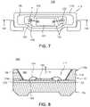
- FIG. 7is a front view illustrating a side-view LED according to a first embodiment of the invention.
- FIG. 8is a cross-sectional view cut along the line VIII-VIII of FIG. 8 ;
- FIG. 9is a cross-sectional view for explaining reflection and heat release by a reflective layer in the side-view LED according to a first embodiment of the invention.
- FIG. 10illustrates heat distribution of the side-view LED in operation according to a first embodiment of the invention
- FIG. 11illustrates heat distribution of the side-view LED in operation according to the prior art
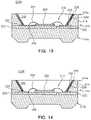
- FIG. 12is a cross-sectional view illustrating a side-view LED corresponding to FIG. 8 according to a second embodiment of the invention.
- FIG. 13is a cross-sectional view illustrating a side-view LED corresponding to FIG. 8 according to a third embodiment of the invention.
- FIG. 14is a cross-sectional view illustrating a side-view LED corresponding to FIG. 8 according to a fourth embodiment of the invention.
- FIGS. 15 a to 15 fare cross-sectional views illustrating a process of manufacturing a side-view LED according to the invention.
- FIG. 7is a front view illustrating the side-view LED according to a first embodiment of the invention and FIG. 8 is a cross-sectional view cut along the line VIII-VIII of FIG. 7 .
- the side-view LED 100As shown in FIGS. 7 and 8 , the side-view LED 100 according to the first embodiment of the invention has an LED window opened to a side to emit light sideward.
- the side-view LED 100is mounted in a backlight device as described above.
- the side-view LED 100includes a pair of lead frames 120 and 122 , an LED chip 102 , a package body 110 , a high reflective metal layer 126 , a transparent encapsulant 140 and an insulating layer 124 .
- the pair of lead frames 120 and 122each act as a terminal.
- the LED chip 102is attached to a portion of the lead frames 120 and 122 and electrically connected thereto.
- the package body 110houses the lead frames 120 and 122 and has a concave 112 formed around the LED chip.
- the high reflective metal layer 126is formed integrally on a wall 114 of the concave 112 .
- the transparent encapsulant 140is filled in the concave 112 to encapsulate the LED chip 102 , while forming the LED window.
- the insulating layer 124is formed on a predetermined area of the lead frames 120 and 122 so that the lead frames are insulated from the high reflective metal layer 126 .
- the LED chip 102 attached to the lead frame 120is electrically connected to the lead frames 120 and 122 via wires 106 .
- the wires 106are bonded to the LED chip 102 and the lead frames 120 and 122 via solders 104 .
- the insulating layer 124is formed on a predetermined area of the lead frames 120 and 122 so that the LED chip 102 can be mounted and the solders 104 are applied in the remaining area thereof. That is, in an area where the LED chip 102 is mounted, the insulating layer 124 is not formed. Also, as shown in FIG. 7 , the insulating layer 124 is not formed in a round opening area H where the solders 104 are applied.
- the insulating layer 124is made of one selected from a group consisting of SiO 2 , SiN, Al 2 O 3 and mixtures thereof.
- the insulating layer 124is formed via deposition such as sputtering and electronic beam method. This produces the insulating layer 124 having a thickness of several ⁇ to several ⁇ m.
- the insulating layer 124has a thickness that enables electrical insulation between the lead frames 120 and 122 and the reflective layer 126 without specific limits.
- the reflective layer 126is made of a high reflective metal, i.e., one selected from a group consisting of Ag, Al, Au, Cu, Pd, Pt, Rd and alloys thereof. Such a metal is deposited to a thickness of several ⁇ to several ⁇ m on the inner surface of the side wall 114 via sputtering or electronic beam method to form the reflective layer 126 .
- the reflective layer 126This allows the reflective layer 126 to exhibit a reflectivity of substantially 90% or more. Therefore light projected onto the side wall 114 from the LED chip 102 is reflected forward, i.e., in an arrow A direction.
- the reflective layer 126exhibits a reflectivity higher than that of resin of the package body 110 .
- the LED 100 of the inventionensures much higher reflection efficiency of the inner wall than the conventional LED, thereby enhancing light efficiency.
- the thickness of the insulating layer 126which is formed via deposition, accordingly can be precisely adjusted and extremely reduced.
- the insulating layer 126reflects light generated from the LED chip 102 forward along with the lead frames 120 and 122 , the light generated from the LED chip 102 rarely reaches the package body 110 .
- the package body 110to be made of a transparent resin as in the transparent encapsulant 140 .
- the package body 110 made of the transparent resinassures good aesthetic appearance.
- the transparent encapsulant 140may contain fluorescent material which converts a short wavelength light generated into a multi-wavelength light, i.e., a multi-color light.
- the transparent encapsulant 140may contain ultraviolet ray absorbent/modifier and diffuser.
- light L generatedexits forward (indicated with A) and outward through the LED window, i.e., the transparent encapsulant 140 . Also, light exiting sideward or backward is reflected by the lead frames 120 and 122 or the reflective layer 126 and exits forward A and outward. At this time, the reflective layer 126 with high reflectivity enhances light efficiency of the LED 100 as described above.
- the reflective layer 126boosts light efficiency and heat release efficiency of the LED 100 .
- FIG. 10is a picture illustrating heat distribution of the side-view LED in operation according to a first embodiment of the invention.
- FIG. 11is a picture illustrating heat distribution of the side-view LED in operation according to the prior art.
- the transparent encapsulant 40has a considerably high temperature and the lead frame 22 having an LED chip 30 mounted thereon exhibits a wide temperature gap with respect to the other lead frame 22 .
- Such a side-view LED of the inventiondemonstrates superior light efficiency and higher heat release efficiency.
- FIG. 12is a cross-sectional view of a side-view LED corresponding to FIG. 8 according to a second embodiment of the invention.
- the side-view LED 200 according to the second embodiment of the inventionis equal to the side view LED 100 according to the first embodiment of the invention except for an intermediate film 228 formed between a side wall 214 and a reflective layer 226 . Therefore, the same components were given numeral signs that increased by 100s and will not be explained further.
- the intermediate film 228is made of an insulator selected from a group consisting of SiO 2 , SiN, Al 2 O 3 and mixtures thereof.
- the intermediate film 228is applied before forming of the reflective layer 226 , preferably via deposition such as sputtering and electronic beam method. This allows the intermediate film 228 to have even a thickness of several ⁇ to several ⁇ m.
- the intermediate film 228 formedfacilitates growth of the reflective layer 226 . That is, in case where metal is directly deposited on an inner surface of a resin side wall 214 , it may be poorly adhered to the side wall 214 depending on the type of metal. However, in case where an insulating intermediate film 228 is formed first and metal is deposited thereon, the metal can be highly bonded to the intermediate layer 228 , thereby producing the excellent reflective layer 226 .
- some resin such as LCPallows metal to be easily deposited, thereby obtaining the excellent reflective layer 226 made of one selected from a group consisting of Ag, Al, Au, Cu, Pd, Pt, Rd and alloys thereof.
- FIG. 13is a cross-sectional view of a side-view LED corresponding to FIG. 8 according to a third embodiment of the invention.
- the side-view LED 200 A according to the third embodiment of the inventionis equal to the side-view LED 200 except for a passivation film 230 formed on the reflective layer 226 . Therefore the same components were given numeral signs that increased by 100s and will not be explained further.
- the passivation film 230 formed on the reflective layer 226is made of an insulating material selected from a group consisting of SiO 2 , SiN, Al 2 O 3 and mixtures thereof like the intermediate film 228 .
- the passivation film 230is disposed to a thickness of several ⁇ to several ⁇ m via sputtering and electronic beam method.
- the passivation film 230serves to prevent debonding of the reflective layer 226 .
- a reflective layer 226is formed and an LED chip is mounted.
- a transparent resinis poured into a concave 212 to form a transparent encapsulant 240 .
- some metal deposited, if in direct contact with resin,may fall off into the resin. This potentially degrades quality of the reflective layer 226 and transparency of the resin encapsulant 240 . Therefore, the passivation film 230 is formed on the metal reflective layer 226 to prevent metal from falling off into the resin, thereby enhancing quality and stability of the metal reflective layer 226 .
- FIG. 14is a cross-sectional view of a side-view LED corresponding to FIG. 8 according to a fourth embodiment of the invention.
- the LED 200 B according to the fourth embodiment of the inventionis distinguished from the LED 200 A according to the third embodiment of FIG. 13 only in that an insulating layer 224 is formed on a joint between a reflective layer 226 and lead frames 220 and 222 . Therefore, the same components were given numeral signs that increased by 100s and will not be explained further.
- the LED of FIGS. 13 and 14can also employ a structure in which the reflective layer 226 and passivation film 230 are formed on the side wall 214 without the intermediate film 228 formed.
- FIGS. 15 a to 15 fillustrate in a stepwise fashion a method for manufacturing the side-view LED according to the invention.
- lead frames 220 and 222are prepared, and an insulating layer 224 is formed thereon with a predetermined pattern.
- the insulating layer 224is formed to expose a predetermined area of the lead frames 220 and 222 .
- the insulating layer 224is formed on a predetermined area of the lead frames 220 and 222 . That is, the insulating layer 224 is formed so that the LED chip 202 is mounted and solders 206 are provided in the remaining area in the following process (see FIG. 15 f ).
- the insulating layer 224is made of one selected from a group consisting of SiO 2 , SiN, Al 2 O 3 and mixtures thereof, preferably via sputtering and electronic beam method. This allows the insulating layer 224 to have even a thickness of several ⁇ to several ⁇ m.
- the insulating layer 224is formed via etching or lift-off.
- an insulating materialis deposited on an entire surface of a subject, or an entire area of lead frames 220 and 222 . Then, the insulating material is etched with a predetermined pattern by using a PR pattern as a mask, and the PR pattern is removed to obtain an insulating layer of a desired pattern.
- the PR patternis first adhered onto a surface of a subject and an insulating material is deposited only in an opening area of the PR pattern by using the PR pattern as a mask. Then the PR pattern is removed to obtain an insulating layer of a desired pattern.
- resinis injected via mold to form a package body 210 as shown in FIG. 15 b .
- a conventional opaque resin and a transparent resincan be adopted for the resin for the package body 210 .
- a screen 250is placed on a bottom of a concave 212 .
- an insulator selected from SiO 2 , SiN and Al 2 O 3is deposited on an inner surface 216 of a side wall 214 to form an intermediate film 228 (refer to FIG. 15 d ) as indicated with an arrow A.
- the screen 250is spaced apart from the inner surface 216 at a predetermined distance.
- the screen 250has a thickness equal to that of the intermediate layer 228 , which ranges from several ⁇ to several ⁇ m.
- the screen 250is removed in an arrow B direction as shown in FIG. 15 d.
- the LED chip 202is mounted on an opening area of the lead frames 220 , and wired 204 and soldered 206 to electrically connect to the lead frames 220 .
- the manufacturing method of the LED as just describedis not only applicable to the LED 100 , 200 , 200 A of the first to third embodiments of the invention but also applicable to other modifications.
- the manufacturing method of the LEDis equally applicable to a modified structure in which the reflective layer 126 , 226 is directly formed on the side wall 114 , 214 of the LED and a passivation film is formed thereon.
- a reflective layer deposited on an inner surface of a side wall of an LEDexhibits excellent reflectivity, thereby boosting light efficiency of the LED. Also, the reflective layer has superior heat release efficiency, thereby improving heat release properties of the LED. In addition, the reflective layer formed via deposition prevents damage in the side wall and LED chip, which is caused by squeezing a plate metal in a narrow concave.
Landscapes
- Led Device Packages (AREA)
Abstract
Description
Claims (13)
Priority Applications (1)
| Application Number | Priority Date | Filing Date | Title |
|---|---|---|---|
| US12/618,445US8268651B2 (en) | 2005-07-04 | 2009-11-13 | Manufacturing method of light emitting diode package |
Applications Claiming Priority (2)
| Application Number | Priority Date | Filing Date | Title |
|---|---|---|---|
| KR1020050059590AKR100665216B1 (en) | 2005-07-04 | 2005-07-04 | Side-side light emitting diode with improved sidewall reflection structure |
| KR10-2005-0059590 | 2005-07-04 |
Related Child Applications (1)
| Application Number | Title | Priority Date | Filing Date |
|---|---|---|---|
| US12/618,445DivisionUS8268651B2 (en) | 2005-07-04 | 2009-11-13 | Manufacturing method of light emitting diode package |
Publications (2)
| Publication Number | Publication Date |
|---|---|
| US20070001187A1 US20070001187A1 (en) | 2007-01-04 |
| US7687815B2true US7687815B2 (en) | 2010-03-30 |
Family
ID=37588397
Family Applications (2)
| Application Number | Title | Priority Date | Filing Date |
|---|---|---|---|
| US11/478,621Expired - Fee RelatedUS7687815B2 (en) | 2005-07-04 | 2006-07-03 | Side-view light emitting diode having improved side-wall reflection structure |
| US12/618,445Expired - Fee RelatedUS8268651B2 (en) | 2005-07-04 | 2009-11-13 | Manufacturing method of light emitting diode package |
Family Applications After (1)
| Application Number | Title | Priority Date | Filing Date |
|---|---|---|---|
| US12/618,445Expired - Fee RelatedUS8268651B2 (en) | 2005-07-04 | 2009-11-13 | Manufacturing method of light emitting diode package |
Country Status (4)
| Country | Link |
|---|---|
| US (2) | US7687815B2 (en) |
| JP (1) | JP4592650B2 (en) |
| KR (1) | KR100665216B1 (en) |
| CN (1) | CN100433390C (en) |
Cited By (11)
| Publication number | Priority date | Publication date | Assignee | Title |
|---|---|---|---|---|
| US20090020839A1 (en)* | 2007-07-09 | 2009-01-22 | Kabushiki Kaisha Toshiba | Semiconductor light receiving device and method for manufacturing same |
| US20100308364A1 (en)* | 2006-03-17 | 2010-12-09 | Seoul Semiconductor Co., Ltd. | Side-view light emitting diode package having a reflector |
| CN102939670A (en)* | 2010-06-16 | 2013-02-20 | 欧司朗光电半导体有限公司 | Optoelectronic devices |
| US8716735B2 (en) | 2011-03-08 | 2014-05-06 | Lextar Electronics Corp. | Light-emitting diode with metal structure and heat sink |
| US20150270461A1 (en)* | 2010-12-28 | 2015-09-24 | Rohm Co., Ltd. | Light emitting element unit and method for manufacturing the same, light emitting element package and illuminating device |
| US20150362136A1 (en)* | 2013-01-25 | 2015-12-17 | Koninklijke Philips N.V. | Lighting assembly and method for manufacturing a lighting assembly |
| US20170263825A1 (en)* | 2014-09-05 | 2017-09-14 | Osram Opto Semiconductors Gmbh | Method for Producing an Optoelectronic Component, and Optoelectronic Component |
| US10260684B2 (en) | 2013-12-17 | 2019-04-16 | Lumileds Llc | Low and high beam LED lamp |
| US10454010B1 (en) | 2006-12-11 | 2019-10-22 | The Regents Of The University Of California | Transparent light emitting diodes |
| US11333320B2 (en) | 2018-10-22 | 2022-05-17 | American Sterilizer Company | Retroreflector LED spectrum enhancement method and apparatus |
| US11435038B2 (en) | 2013-01-25 | 2022-09-06 | Lumileds Llc | Lighting assembly and method for manufacturing a lighting assembly |
Families Citing this family (77)
| Publication number | Priority date | Publication date | Assignee | Title |
|---|---|---|---|---|
| USD538239S1 (en)* | 2003-07-28 | 2007-03-13 | Nichia Corp. | Light emitting diode |
| USD566058S1 (en)* | 2003-07-28 | 2008-04-08 | Nichia Corporation | Light emitting diode |
| JP2006108333A (en)* | 2004-10-04 | 2006-04-20 | Toyoda Gosei Co Ltd | lamp |
| TWD124439S1 (en)* | 2006-03-24 | 2008-08-21 | 首爾半導體股份有限公司 | Light emitting diode (led) |
| TWD124440S1 (en)* | 2006-03-30 | 2008-08-21 | 首爾半導體股份有限公司 | Light emitting diode (led) |
| JP2008016565A (en)* | 2006-07-04 | 2008-01-24 | Shinko Electric Ind Co Ltd | LIGHT EMITTING ELEMENT CONTAINER, MANUFACTURING METHOD THEREOF, AND LIGHT EMITTING DEVICE |
| US7910938B2 (en)* | 2006-09-01 | 2011-03-22 | Cree, Inc. | Encapsulant profile for light emitting diodes |
| JP4846498B2 (en)* | 2006-09-22 | 2011-12-28 | 株式会社東芝 | Optical semiconductor device and method for manufacturing optical semiconductor device |
| TWI329934B (en)* | 2007-01-17 | 2010-09-01 | Chi Mei Lighting Tech Corp | Lead frame structure of light emitting diode |
| KR101352921B1 (en)* | 2007-05-25 | 2014-01-24 | 삼성디스플레이 주식회사 | Light source module, back-light assembly having the light source module and display apparatus having the back-light assembly |
| WO2009014590A2 (en) | 2007-06-25 | 2009-01-29 | Qd Vision, Inc. | Compositions and methods including depositing nanomaterial |
| US20090026470A1 (en)* | 2007-07-23 | 2009-01-29 | Novalite Optronics Corp. | Super thin side-view light-emitting diode (led) package and fabrication method thereof |
| KR100928635B1 (en)* | 2007-08-30 | 2009-11-27 | 주식회사 루멘스 | Side Light Emitting Diode Package |
| TWD124993S1 (en)* | 2007-10-05 | 2008-09-21 | 顯明電子股份有限公司 | LED |
| WO2009074919A1 (en) | 2007-12-11 | 2009-06-18 | Koninklijke Philips Electronics N.V. | Side emitting device with hybrid top reflector |
| US8471281B2 (en) | 2007-12-11 | 2013-06-25 | Koninklijke Philips Electronics N.V. | Side emitting device with hybrid top reflector |
| JP5426091B2 (en)* | 2007-12-27 | 2014-02-26 | 豊田合成株式会社 | Light emitting device |
| KR100969144B1 (en)* | 2008-01-28 | 2010-07-08 | 알티전자 주식회사 | Light emitting diode package |
| JP2011512006A (en)* | 2008-01-30 | 2011-04-14 | デジタル オプティクス インターナショナル,リミティド ライアビリティ カンパニー | Thin lighting system |
| US8721149B2 (en) | 2008-01-30 | 2014-05-13 | Qualcomm Mems Technologies, Inc. | Illumination device having a tapered light guide |
| CN101499506B (en)* | 2008-01-30 | 2012-06-13 | 旭丽电子(广州)有限公司 | LED element |
| USD601518S1 (en)* | 2008-02-22 | 2009-10-06 | Alti-Electronics Co., Ltd | Light emitting diode |
| USD596148S1 (en)* | 2008-02-22 | 2009-07-14 | Alti-Electronics Co., Ltd | Light emitting diode |
| USD595677S1 (en)* | 2008-02-22 | 2009-07-07 | Alti-Electronics Co., Ltd | Light emitting diode |
| TWD130667S1 (en)* | 2008-02-22 | 2009-09-01 | 電子股份有限公司 | Light emitting diode |
| USD601516S1 (en) | 2008-02-25 | 2009-10-06 | Seoul Semiconductor Co., Ltd. | Light emitting diode (LED) |
| KR20090100117A (en)* | 2008-03-19 | 2009-09-23 | 삼성전자주식회사 | Backlight unit and liquid crystal display including the same |
| USD605609S1 (en)* | 2008-05-21 | 2009-12-08 | Alti-Electronics Co., Ltd | Light emitting diode |
| USD605608S1 (en)* | 2008-05-21 | 2009-12-08 | Alti-Electronics Co., Ltd | Light emitting diode |
| USD606032S1 (en)* | 2008-05-21 | 2009-12-15 | Alti-Electronics Co., Ltd. | Light emitting diode |
| US20100051089A1 (en)* | 2008-09-02 | 2010-03-04 | Qualcomm Mems Technologies, Inc. | Light collection device with prismatic light turning features |
| US8358266B2 (en) | 2008-09-02 | 2013-01-22 | Qualcomm Mems Technologies, Inc. | Light turning device with prismatic light turning features |
| JP5492899B2 (en)* | 2008-10-10 | 2014-05-14 | クォルコム・メムズ・テクノロジーズ・インコーポレーテッド | Distributed lighting system |
| EP2351464A4 (en)* | 2008-10-10 | 2013-10-09 | Qualcomm Mems Technologies Inc | DECENTRALIZED LIGHTING CONTROL SYSTEM |
| TW201020643A (en)* | 2008-11-25 | 2010-06-01 | Chi Mei Lighting Tech Corp | Side view type light-emitting diode package structure, and manufacturing method and application thereof |
| JPWO2010067701A1 (en)* | 2008-12-12 | 2012-05-17 | 三洋電機株式会社 | Light emitting device, light emitting device module, and method of manufacturing light emitting device |
| JP2010153861A (en)* | 2008-12-15 | 2010-07-08 | Yiguang Electronic Ind Co Ltd | Light emitting diode package structure |
| KR20110104090A (en)* | 2009-01-13 | 2011-09-21 | 퀄컴 엠이엠스 테크놀로지스, 인크. | Large Area Light Panels and Screens |
| CN101800275B (en)* | 2009-02-11 | 2012-09-05 | 奇力光电科技股份有限公司 | Side-view light-emitting diode packaging structure and its manufacturing method and application |
| CN102449512A (en)* | 2009-05-29 | 2012-05-09 | 高通Mems科技公司 | Illumination devices and methods of fabrication thereof |
| TWD138645S1 (en)* | 2009-12-11 | 2011-01-11 | 億光電子工業股份有限公司 | Light emitting diode |
| KR100986571B1 (en)* | 2010-02-04 | 2010-10-07 | 엘지이노텍 주식회사 | Package of light emitting device and method for fabricating the same |
| US8402647B2 (en) | 2010-08-25 | 2013-03-26 | Qualcomm Mems Technologies Inc. | Methods of manufacturing illumination systems |
| CN102479906A (en)* | 2010-11-24 | 2012-05-30 | 展晶科技(深圳)有限公司 | Light-emitting diode packaging structure |
| CN102479909B (en)* | 2010-11-24 | 2014-12-10 | 展晶科技(深圳)有限公司 | Light emitting diode |
| CN103384794B (en)* | 2010-12-23 | 2018-05-29 | 三星电子株式会社 | Optical components containing quantum dots |
| CN102593307A (en)* | 2011-01-07 | 2012-07-18 | 钰桥半导体股份有限公司 | Light-emitting diode optical reflective structure |
| TWI462348B (en)* | 2011-01-27 | 2014-11-21 | 矽品精密工業股份有限公司 | Light emitting device and fabrication method thereof |
| JP4904604B1 (en)* | 2011-02-17 | 2012-03-28 | 国立大学法人九州工業大学 | LED module device and manufacturing method thereof |
| TWI517452B (en)* | 2011-03-02 | 2016-01-11 | 建準電機工業股份有限公司 | Polycrystalline package structure of luminescent crystal |
| KR20120108437A (en)* | 2011-03-24 | 2012-10-05 | 삼성전자주식회사 | Light emitting device package |
| CN202094168U (en)* | 2011-05-03 | 2011-12-28 | 深圳市华星光电技术有限公司 | Led packaging structure |
| KR101830717B1 (en)* | 2011-06-30 | 2018-02-21 | 엘지이노텍 주식회사 | A light emitting device pakage |
| US8992045B2 (en)* | 2011-07-22 | 2015-03-31 | Guardian Industries Corp. | LED lighting systems and/or methods of making the same |
| KR101824011B1 (en)* | 2011-07-29 | 2018-01-31 | 엘지이노텍 주식회사 | Light-emitting device |
| KR20130022052A (en)* | 2011-08-24 | 2013-03-06 | 엘지이노텍 주식회사 | The light emitting device package and the light emitting system |
| CN102544318B (en)* | 2012-01-04 | 2015-06-03 | 歌尔声学股份有限公司 | Light-emitting diode device |
| KR20130118552A (en)* | 2012-04-20 | 2013-10-30 | 엘지이노텍 주식회사 | Light emitting device package and light emitting apparatus having the same |
| CN103682059B (en)* | 2012-09-05 | 2016-08-17 | 长华电材股份有限公司 | Pre-process method and structure of light-emitting diode packaging |
| CN103794698B (en)* | 2012-10-31 | 2016-12-21 | 展晶科技(深圳)有限公司 | Light emitting diode |
| JP2013030812A (en)* | 2012-11-06 | 2013-02-07 | Mitsubishi Chemicals Corp | Substrate for led chip fixation and method of manufacturing the same |
| JP6175952B2 (en)* | 2013-07-19 | 2017-08-09 | 日亜化学工業株式会社 | Light emitting device |
| US9673364B2 (en) | 2013-07-19 | 2017-06-06 | Nichia Corporation | Light emitting device and method of manufacturing the same |
| KR102123039B1 (en) | 2013-07-19 | 2020-06-15 | 니치아 카가쿠 고교 가부시키가이샤 | Light emitting device and method of manufacturing the same |
| DE102013219063A1 (en) | 2013-09-23 | 2015-03-26 | Osram Opto Semiconductors Gmbh | Optoelectronic component and method for its production |
| CN104716245A (en)* | 2013-12-13 | 2015-06-17 | 晶元光电股份有限公司 | Light emitting device and manufacturing method thereof |
| US9630333B2 (en)* | 2014-03-31 | 2017-04-25 | Sphynx Collection, Llc | Travel razor |
| JP6671117B2 (en)* | 2014-07-08 | 2020-03-25 | エルジー イノテック カンパニー リミテッド | Light emitting device package |
| US10340433B2 (en) | 2015-01-19 | 2019-07-02 | Lg Innotek Co., Ltd. | Light emitting device |
| DE102015102785A1 (en)* | 2015-02-26 | 2016-09-01 | Osram Opto Semiconductors Gmbh | Optoelectronic lighting device |
| KR102237155B1 (en) | 2015-03-11 | 2021-04-07 | 엘지이노텍 주식회사 | Light emitting device and light unit having thereof |
| JP6638282B2 (en)* | 2015-09-25 | 2020-01-29 | 三菱マテリアル株式会社 | Light emitting module with cooler and method of manufacturing light emitting module with cooler |
| EP3166146B1 (en)* | 2015-11-06 | 2019-04-17 | ams AG | Optical package and method of producing an optical package |
| JP6361645B2 (en)* | 2015-12-22 | 2018-07-25 | 日亜化学工業株式会社 | Light emitting device |
| CN106129226A (en)* | 2016-08-31 | 2016-11-16 | 苏州市悠文电子有限公司 | Light emitting diode is sent out in side |
| JP7140956B2 (en)* | 2017-10-25 | 2022-09-22 | 日亜化学工業株式会社 | Light-emitting device, package and manufacturing method thereof |
| CN115000272A (en)* | 2018-12-14 | 2022-09-02 | 泉州三安半导体科技有限公司 | Light emitting diode package |
Citations (9)
| Publication number | Priority date | Publication date | Assignee | Title |
|---|---|---|---|---|
| JPH10215001A (en) | 1997-01-31 | 1998-08-11 | Nichia Chem Ind Ltd | Light emitting device |
| JPH11500584A (en) | 1996-09-20 | 1999-01-12 | シーメンス アクチエンゲゼルシヤフト | Casting material for wavelength conversion, method of using the same, and method of manufacturing the same |
| JP2002190619A (en) | 2000-12-22 | 2002-07-05 | Toshiba Corp | Semiconductor light emitting device and method of manufacturing the same |
| US20020167485A1 (en)* | 2001-03-02 | 2002-11-14 | Innovative Solutions & Support, Inc. | Image display generator for a head-up display |
| US6614103B1 (en)* | 2000-09-01 | 2003-09-02 | General Electric Company | Plastic packaging of LED arrays |
| JP2003273405A (en) | 2002-03-19 | 2003-09-26 | Kyocera Corp | Light emitting element storage package |
| JP2005019919A (en) | 2003-06-30 | 2005-01-20 | Toyoda Gosei Co Ltd | Light emitting device |
| JP2005109289A (en) | 2003-10-01 | 2005-04-21 | Nichia Chem Ind Ltd | Light emitting device |
| US20050093146A1 (en) | 2003-10-30 | 2005-05-05 | Kensho Sakano | Support body for semiconductor element, method for manufacturing the same and semiconductor device |
Family Cites Families (4)
| Publication number | Priority date | Publication date | Assignee | Title |
|---|---|---|---|---|
| JP2000277813A (en) | 1999-03-26 | 2000-10-06 | Matsushita Electric Works Ltd | Light source device |
| JP2002043632A (en)* | 2000-07-21 | 2002-02-08 | Citizen Electronics Co Ltd | Light emitting diode |
| JP2003046137A (en) | 2001-07-27 | 2003-02-14 | Matsushita Electric Ind Co Ltd | Semiconductor light emitting device |
| KR20040092512A (en)* | 2003-04-24 | 2004-11-04 | (주)그래픽테크노재팬 | A semiconductor light emitting device with reflectors having a cooling function |
- 2005
- 2005-07-04KRKR1020050059590Apatent/KR100665216B1/ennot_activeExpired - Fee Related
- 2006
- 2006-07-03USUS11/478,621patent/US7687815B2/ennot_activeExpired - Fee Related
- 2006-07-04JPJP2006184094Apatent/JP4592650B2/ennot_activeExpired - Fee Related
- 2006-07-04CNCNB2006100957598Apatent/CN100433390C/ennot_activeExpired - Fee Related
- 2009
- 2009-11-13USUS12/618,445patent/US8268651B2/ennot_activeExpired - Fee Related
Patent Citations (11)
| Publication number | Priority date | Publication date | Assignee | Title |
|---|---|---|---|---|
| JPH11500584A (en) | 1996-09-20 | 1999-01-12 | シーメンス アクチエンゲゼルシヤフト | Casting material for wavelength conversion, method of using the same, and method of manufacturing the same |
| US6066861A (en) | 1996-09-20 | 2000-05-23 | Siemens Aktiengesellschaft | Wavelength-converting casting composition and its use |
| JPH10215001A (en) | 1997-01-31 | 1998-08-11 | Nichia Chem Ind Ltd | Light emitting device |
| US6614103B1 (en)* | 2000-09-01 | 2003-09-02 | General Electric Company | Plastic packaging of LED arrays |
| JP2002190619A (en) | 2000-12-22 | 2002-07-05 | Toshiba Corp | Semiconductor light emitting device and method of manufacturing the same |
| US20020167485A1 (en)* | 2001-03-02 | 2002-11-14 | Innovative Solutions & Support, Inc. | Image display generator for a head-up display |
| JP2003273405A (en) | 2002-03-19 | 2003-09-26 | Kyocera Corp | Light emitting element storage package |
| JP2005019919A (en) | 2003-06-30 | 2005-01-20 | Toyoda Gosei Co Ltd | Light emitting device |
| JP2005109289A (en) | 2003-10-01 | 2005-04-21 | Nichia Chem Ind Ltd | Light emitting device |
| US20050093146A1 (en) | 2003-10-30 | 2005-05-05 | Kensho Sakano | Support body for semiconductor element, method for manufacturing the same and semiconductor device |
| JP2005159311A (en) | 2003-10-30 | 2005-06-16 | Nichia Chem Ind Ltd | Support for semiconductor element, method for manufacturing the same, and semiconductor device |
Non-Patent Citations (2)
| Title |
|---|
| Chinese Office Action, with English Translation, issued in corresponding Chinese Patent Application No. 200610095798, dated on Sep. 7, 2007. |
| Japanese Office Action issued in Japanese Patent Application No. JP 2006-184094, dated Jun. 16, 2009. |
Cited By (23)
| Publication number | Priority date | Publication date | Assignee | Title |
|---|---|---|---|---|
| US20100308364A1 (en)* | 2006-03-17 | 2010-12-09 | Seoul Semiconductor Co., Ltd. | Side-view light emitting diode package having a reflector |
| US8138514B2 (en)* | 2006-03-17 | 2012-03-20 | Seoul Semiconductor Co., Ltd. | Side-view light emitting diode package having a reflector |
| US10454010B1 (en) | 2006-12-11 | 2019-10-22 | The Regents Of The University Of California | Transparent light emitting diodes |
| US10658557B1 (en) | 2006-12-11 | 2020-05-19 | The Regents Of The University Of California | Transparent light emitting device with light emitting diodes |
| US10644213B1 (en) | 2006-12-11 | 2020-05-05 | The Regents Of The University Of California | Filament LED light bulb |
| US10593854B1 (en) | 2006-12-11 | 2020-03-17 | The Regents Of The University Of California | Transparent light emitting device with light emitting diodes |
| US7880254B2 (en)* | 2007-07-09 | 2011-02-01 | Kabushiki Kaisha Toshiba | Semiconductor light receiving device and method for manufacturing same |
| US20090020839A1 (en)* | 2007-07-09 | 2009-01-22 | Kabushiki Kaisha Toshiba | Semiconductor light receiving device and method for manufacturing same |
| US20130200411A1 (en)* | 2010-06-16 | 2013-08-08 | Osram Opto Semiconductors Gmbh | Optoelectronic component |
| CN102939670A (en)* | 2010-06-16 | 2013-02-20 | 欧司朗光电半导体有限公司 | Optoelectronic devices |
| CN102939670B (en)* | 2010-06-16 | 2015-11-25 | 欧司朗光电半导体有限公司 | Opto-electronic device |
| US8759862B2 (en)* | 2010-06-16 | 2014-06-24 | Osram Opto Semiconductors Gmbh | Optoelectronic component |
| US20150270461A1 (en)* | 2010-12-28 | 2015-09-24 | Rohm Co., Ltd. | Light emitting element unit and method for manufacturing the same, light emitting element package and illuminating device |
| US9997682B2 (en)* | 2010-12-28 | 2018-06-12 | Rohm Co., Ltd. | Light emitting element unit and method for manufacturing the same, light emitting element package and illuminating device |
| US8716735B2 (en) | 2011-03-08 | 2014-05-06 | Lextar Electronics Corp. | Light-emitting diode with metal structure and heat sink |
| US10551011B2 (en)* | 2013-01-25 | 2020-02-04 | Lumileds Llc | Lighting assembly and method for manufacturing a lighting assembly |
| US20150362136A1 (en)* | 2013-01-25 | 2015-12-17 | Koninklijke Philips N.V. | Lighting assembly and method for manufacturing a lighting assembly |
| US11435038B2 (en) | 2013-01-25 | 2022-09-06 | Lumileds Llc | Lighting assembly and method for manufacturing a lighting assembly |
| US12007081B2 (en) | 2013-01-25 | 2024-06-11 | Lumileds Llc | Lighting assembly and method for manufacturing a lighting assembly |
| US10260684B2 (en) | 2013-12-17 | 2019-04-16 | Lumileds Llc | Low and high beam LED lamp |
| US9899574B2 (en)* | 2014-09-05 | 2018-02-20 | Osram Opto Semiconductor Gmbh | Method for producing an optoelectronic component, and optoelectronic component |
| US20170263825A1 (en)* | 2014-09-05 | 2017-09-14 | Osram Opto Semiconductors Gmbh | Method for Producing an Optoelectronic Component, and Optoelectronic Component |
| US11333320B2 (en) | 2018-10-22 | 2022-05-17 | American Sterilizer Company | Retroreflector LED spectrum enhancement method and apparatus |
Also Published As
| Publication number | Publication date |
|---|---|
| CN100433390C (en) | 2008-11-12 |
| JP2007019505A (en) | 2007-01-25 |
| JP4592650B2 (en) | 2010-12-01 |
| US20100120182A1 (en) | 2010-05-13 |
| CN1893130A (en) | 2007-01-10 |
| US20070001187A1 (en) | 2007-01-04 |
| KR100665216B1 (en) | 2007-01-09 |
| US8268651B2 (en) | 2012-09-18 |
Similar Documents
| Publication | Publication Date | Title |
|---|---|---|
| US7687815B2 (en) | Side-view light emitting diode having improved side-wall reflection structure | |
| JP7381974B2 (en) | light emitting device | |
| KR101314414B1 (en) | Lighting assembly | |
| US8106584B2 (en) | Light emitting device and illumination apparatus | |
| US7999280B2 (en) | Light emitting diode package employing lead terminal with reflecting surface | |
| RU2717381C2 (en) | Light-emitting device, integrated light-emitting device and light-emitting module | |
| JP2020004895A (en) | Light-emitting device | |
| JP7522529B2 (en) | Light-emitting device | |
| JP3872490B2 (en) | Light emitting element storage package, light emitting device, and lighting device | |
| CN101023533A (en) | Housing for an optoelectronic component, optoelectronic component and method for the production of an optoelectronic component | |
| JP2006519481A (en) | Illumination module and method of manufacturing the illumination module | |
| KR20060123965A (en) | Backlight unit with light emitting diode | |
| CN110197864B (en) | Semiconductor light emitting device and method of manufacturing the same | |
| JP5103841B2 (en) | Light emitting module and backlight device using the same | |
| CN100487936C (en) | Semiconductor light emitting device, semiconductor element, and method for fabricating the semiconductor light emitting device | |
| JP2005340472A (en) | Light emitting device and lighting device | |
| JP2007184541A (en) | LIGHT EMITTING MODULE, ITS MANUFACTURING METHOD, AND BACKLIGHT DEVICE USING THE SAME | |
| JP2007184534A (en) | LIGHT EMITTING MODULE, ITS MANUFACTURING METHOD, AND BACKLIGHT DEVICE USING THE SAME | |
| KR100691178B1 (en) | Side light emitting diode with light emitting diode chip placed behind the lead frame | |
| CN105845806B (en) | Light emitting device package | |
| KR101831274B1 (en) | Light Emitting Diode Package and Electronic Device | |
| JP2006128322A (en) | Light emitting device and lighting device | |
| JP2006351611A (en) | Substrate for mounting light-emitting device and optical semiconductor device using same | |
| JP4480736B2 (en) | Light emitting device | |
| JPH11177130A (en) | Led lamp |
Legal Events
| Date | Code | Title | Description |
|---|---|---|---|
| AS | Assignment | Owner name:SAMSUNG ELECTRO-MECHANICS, CO., LTD.,KOREA, REPUBL Free format text:ASSIGNMENT OF ASSIGNORS INTEREST;ASSIGNOR:KIM, HONG MIN;REEL/FRAME:018070/0455 Effective date:20060622 Owner name:SAMSUNG ELECTRO-MECHANICS, CO., LTD., KOREA, REPUB Free format text:ASSIGNMENT OF ASSIGNORS INTEREST;ASSIGNOR:KIM, HONG MIN;REEL/FRAME:018070/0455 Effective date:20060622 | |
| FEPP | Fee payment procedure | Free format text:PAYOR NUMBER ASSIGNED (ORIGINAL EVENT CODE: ASPN); ENTITY STATUS OF PATENT OWNER: LARGE ENTITY | |
| STCF | Information on status: patent grant | Free format text:PATENTED CASE | |
| AS | Assignment | Owner name:SAMSUNG LED CO., LTD., KOREA, REPUBLIC OF Free format text:ASSIGNMENT OF ASSIGNORS INTEREST;ASSIGNOR:SAMSUNG ELECTRO-MECHANICS CO., LTD.;REEL/FRAME:024723/0532 Effective date:20100712 | |
| AS | Assignment | Owner name:SAMSUNG ELECTRONICS CO., LTD., KOREA, REPUBLIC OF Free format text:MERGER;ASSIGNOR:SAMSUNG LED CO., LTD.;REEL/FRAME:028744/0272 Effective date:20120403 | |
| FPAY | Fee payment | Year of fee payment:4 | |
| MAFP | Maintenance fee payment | Free format text:PAYMENT OF MAINTENANCE FEE, 8TH YEAR, LARGE ENTITY (ORIGINAL EVENT CODE: M1552) Year of fee payment:8 | |
| FEPP | Fee payment procedure | Free format text:MAINTENANCE FEE REMINDER MAILED (ORIGINAL EVENT CODE: REM.); ENTITY STATUS OF PATENT OWNER: LARGE ENTITY | |
| LAPS | Lapse for failure to pay maintenance fees | Free format text:PATENT EXPIRED FOR FAILURE TO PAY MAINTENANCE FEES (ORIGINAL EVENT CODE: EXP.); ENTITY STATUS OF PATENT OWNER: LARGE ENTITY | |
| STCH | Information on status: patent discontinuation | Free format text:PATENT EXPIRED DUE TO NONPAYMENT OF MAINTENANCE FEES UNDER 37 CFR 1.362 | |
| FP | Lapsed due to failure to pay maintenance fee | Effective date:20220330 |