US7683437B2 - Semiconductor device having fin field effect transistor and manufacturing method thereof - Google Patents
Semiconductor device having fin field effect transistor and manufacturing method thereofDownload PDFInfo
- Publication number
- US7683437B2 US7683437B2US11/896,050US89605007AUS7683437B2US 7683437 B2US7683437 B2US 7683437B2US 89605007 AUS89605007 AUS 89605007AUS 7683437 B2US7683437 B2US 7683437B2
- Authority
- US
- United States
- Prior art keywords
- region
- active region
- semiconductor device
- gate electrode
- source
- Prior art date
- Legal status (The legal status is an assumption and is not a legal conclusion. Google has not performed a legal analysis and makes no representation as to the accuracy of the status listed.)
- Active, expires
Links
- 239000004065semiconductorSubstances0.000titleclaimsabstractdescription61
- 238000004519manufacturing processMethods0.000titleabstractdescription19
- 238000002353field-effect transistor methodMethods0.000title1
- 239000000758substrateSubstances0.000claimsabstractdescription25
- XUIMIQQOPSSXEZ-UHFFFAOYSA-NSiliconChemical compound[Si]XUIMIQQOPSSXEZ-UHFFFAOYSA-N0.000claimsdescription14
- 229910052710siliconInorganic materials0.000claimsdescription14
- 239000010703siliconSubstances0.000claimsdescription14
- 230000000694effectsEffects0.000abstractdescription13
- 229910052581Si3N4Inorganic materials0.000description19
- HQVNEWCFYHHQES-UHFFFAOYSA-Nsilicon nitrideChemical compoundN12[Si]34N5[Si]62N3[Si]51N64HQVNEWCFYHHQES-UHFFFAOYSA-N0.000description19
- 238000002955isolationMethods0.000description14
- VYPSYNLAJGMNEJ-UHFFFAOYSA-NSilicium dioxideChemical compoundO=[Si]=OVYPSYNLAJGMNEJ-UHFFFAOYSA-N0.000description12
- 239000010410layerSubstances0.000description12
- 229910052814silicon oxideInorganic materials0.000description12
- 238000005468ion implantationMethods0.000description10
- 230000015572biosynthetic processEffects0.000description9
- 239000012535impuritySubstances0.000description4
- 229920002120photoresistant polymerPolymers0.000description4
- 230000006866deteriorationEffects0.000description3
- 230000005669field effectEffects0.000description3
- 230000005684electric fieldEffects0.000description2
- 238000005530etchingMethods0.000description2
- 238000002513implantationMethods0.000description2
- 230000006872improvementEffects0.000description2
- 239000011229interlayerSubstances0.000description2
- 230000004048modificationEffects0.000description2
- 238000012986modificationMethods0.000description2
- 230000009467reductionEffects0.000description2
- 230000001133accelerationEffects0.000description1
- 238000001312dry etchingMethods0.000description1
- 230000006870functionEffects0.000description1
- 239000007943implantSubstances0.000description1
- 150000002500ionsChemical class0.000description1
- 238000000034methodMethods0.000description1
- 230000003647oxidationEffects0.000description1
- 238000007254oxidation reactionMethods0.000description1
- 238000000059patterningMethods0.000description1
- 238000005498polishingMethods0.000description1
- 239000000126substanceSubstances0.000description1
- 238000001039wet etchingMethods0.000description1
Images


Classifications
- H—ELECTRICITY
- H10—SEMICONDUCTOR DEVICES; ELECTRIC SOLID-STATE DEVICES NOT OTHERWISE PROVIDED FOR
- H10D—INORGANIC ELECTRIC SEMICONDUCTOR DEVICES
- H10D30/00—Field-effect transistors [FET]
- H10D30/01—Manufacture or treatment
- H10D30/021—Manufacture or treatment of FETs having insulated gates [IGFET]
- H10D30/024—Manufacture or treatment of FETs having insulated gates [IGFET] of fin field-effect transistors [FinFET]
- H—ELECTRICITY
- H10—SEMICONDUCTOR DEVICES; ELECTRIC SOLID-STATE DEVICES NOT OTHERWISE PROVIDED FOR
- H10B—ELECTRONIC MEMORY DEVICES
- H10B12/00—Dynamic random access memory [DRAM] devices
- H10B12/01—Manufacture or treatment
- H10B12/02—Manufacture or treatment for one transistor one-capacitor [1T-1C] memory cells
- H10B12/05—Making the transistor
- H10B12/053—Making the transistor the transistor being at least partially in a trench in the substrate
- H—ELECTRICITY
- H10—SEMICONDUCTOR DEVICES; ELECTRIC SOLID-STATE DEVICES NOT OTHERWISE PROVIDED FOR
- H10B—ELECTRONIC MEMORY DEVICES
- H10B12/00—Dynamic random access memory [DRAM] devices
- H10B12/01—Manufacture or treatment
- H10B12/02—Manufacture or treatment for one transistor one-capacitor [1T-1C] memory cells
- H10B12/05—Making the transistor
- H10B12/056—Making the transistor the transistor being a FinFET
- H—ELECTRICITY
- H10—SEMICONDUCTOR DEVICES; ELECTRIC SOLID-STATE DEVICES NOT OTHERWISE PROVIDED FOR
- H10D—INORGANIC ELECTRIC SEMICONDUCTOR DEVICES
- H10D30/00—Field-effect transistors [FET]
- H10D30/60—Insulated-gate field-effect transistors [IGFET]
- H10D30/62—Fin field-effect transistors [FinFET]
- H10D30/6211—Fin field-effect transistors [FinFET] having fin-shaped semiconductor bodies integral with the bulk semiconductor substrates
Definitions
- the present inventionrelates to a semiconductor device and a semiconductor device manufacturing method, and, more particularly to a semiconductor device including fin field effect transistors and a manufacturing method thereof.
- a gate length of a memory cell transistoris inevitably reduced.
- the gate lengthis smaller, then the short channel effect of the transistor disadvantageously becomes more conspicuous, and sub-threshold current is disadvantageously increased.
- substrate concentrationis increased to suppress the short channel effect and the increase of the sub-threshold current, junction leakage increases. Due to this, the DRAM is confronted with a serious problem of deterioration in refresh characteristics.
- fin-FETfin field effect transistor
- the fin-FETis expected to be able to realize acceleration of operating rate, increase in ON-current, reduction in power consumption and the like, as compared with a planer transistor.
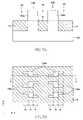
- a structure of a conventional fin-FETwill be described below with reference to FIGS. 14A and 14B .
- FIG. 14Ais a general perspective view showing the structure of the conventional fin-FET
- FIG. 14Bis a general cross-sectional view taken along a line A-A of FIG. 14A .
- a trench 201 t for STI(Shallow Trench Isolation) (hereinafter, “STI trench 201 t ”) is formed in a semiconductor substrate 200 and an element isolation film 2011 is buried in the STI trench 201 t by a predetermined depth from a bottom of the STI trench 201 t .
- the active region 202includes a central portion 202 a and portions 202 b and 202 c located on both sides of the central portion 202 a , respectively.
- a gate electrode 203is formed to cover an upper surface and both side surfaces of the fin-shaped active region 202 in the central portion 202 a of the fin-shaped active region 202 .
- a source region 202 s and a drain region 202 dare formed in the active region 202 and a channel region 202 n is formed between the source region 202 s and the drain region 202 d as shown in FIG. 14B .
- the source region 202 s and the drain region 202 dit is preferable to form the source region 202 s and the drain region 202 d to be deep so that three surfaces, i.e., an upper surface and two side surfaces of the central portion 202 a of the active region 202 function as channels. Due to this, the ion implantation needs to be performed with high energy to form the source and drain regions 202 s and 202 d.
- the source and drain regions 202 s and 202 dare diffused into the channel region 202 n covered with the gate electrode 203 as shown in FIG. 14B .
- a gate lengthis smaller, a distance between the source and drain regions 202 s and 202 d shown as two-headed arrow in FIG. 14B is narrower, with the result that the short channel effect cannot be ignored.
- a concentration of the channel region 202 nmay be increased.
- a devicee.g., a DRAM memory cell, in which it is necessary to suppress junction leakage
- junction electric fieldis deteriorated.
- the deterioration in junction electric fielddisadvantageously increases the junction leakage, resulting in deterioration in data holding characteristics.
- an object of the present inventionto provide a semiconductor device including fin-FETs capable of suppressing both OFF-current resulting from the short channel effect and junction leakage, and a manufacturing method thereof.
- a semiconductor devicecomprising: an active region defined to have a crank shape by an STI region formed on a semiconductor substrate, the active region having an upper surface higher than an upper surface of the STI region; a source region and a drain region formed on both ends of the active region, respectively; a channel region formed between the source region and the drain region in the active region; and a gate electrode covering an upper surface and side surfaces of a central portion of the active region including the channel region.
- a semiconductor devicecomprising: a fin-shaped active region formed by a part of a semiconductor substrate; and a gate electrode extending in an X direction to cross the active region, and covering an upper surface and side surfaces of an almost central portion of the active region, wherein the active region has a channel region covered by the gate electrode and a source region and a drain region formed on both ends of the active region, respectively, wherein the source region and the drain region are offset each other in the X direction.
- a semiconductor devicecomprising: a fin-shaped active region; a gate electrode covering a first portion of the active region; and a source region and a drain region provided on a second portion and a third portion opposed to each other across the first portion of the active region, respectively, wherein the first portion includes at least one bent portion.
- the at least one bent portionincludes a first bent portion and a second bent portion, and a region between the first bent portion and the second bent portion in the active region extends in a direction substantially identical to an extension direction of the gate electrode.
- a semiconductor devicecomprising: a fin-shaped active region including a first portion extending in a first direction, a second portion connected to one end of the first portion and extending in a second direction, and a third portion connected to other end of the first portion and extending in the second direction; a gate electrode extending in the first direction and covering the first portion, a part of the second portion, and a part of the third portion; a source region provided on another part of the second portion; and a drain region provided on another part of the third portion.
- a method of manufacturing a semiconductor devicecomprising: a step of forming a mask layer on a semiconductor substrate, the mask layer having a crank shape in a plan view; a step of etching the semiconductor substrate using the mask layer having the crank shape to form a trench in the semiconductor substrate; a step of burying an element isolation insulating film halfway in the trench to form a fin-shaped active region protruding from an upper surface of the element isolation insulating film, the fin-shaped active region having the crank shape in the plane view, a step of removing the mask layer; a step of forming a gate electrode extending in a direction perpendicular to a major axis direction of the fin-shaped active region, and covering an upper surface and side surfaces of an almost central portion of the active region; and a step of performing ion implantation with the gate electrode used as a mask to form a source region and a drain region on both ends of the fin-shaped active region, respectively.
- the fin-shaped active regionby using the fin-shaped active region, it is expected to realize an improvement in operating rate, an improvement in ON-current, a reduction in power consumption, and the like. Furthermore, a channel region is arranged between a source region and a drain region and the source region and the drain region are not in alignment. Due to this, even if the source region and the drain region are diffused into a region under a gate electrode by performing ion implantation for forming the source region and the drain region with high energy, the short channel effect can be suppressed without increasing a concentration of the channel region.
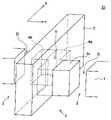
- FIG. 1is a general perspective view for explaining an outline of a semiconductor device according to an embodiment of the present invention
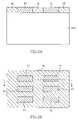
- FIG. 2is a cross-sectional view and a plane view showing a step (formation of a silicon nitride film 11 and a silicon oxide film 12 ) in a method of manufacturing the semiconductor device according to the embodiment of the present invention
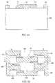
- FIG. 3is a cross-sectional view and a plane view showing a step (formation of a photoresist 13 ) in the method of manufacturing the semiconductor device according to the embodiment of the present invention
- FIG. 4is a cross-sectional view and a plane view showing a step (patterning of the silicon nitride film 11 and the silicon oxide film 12 ) in the method of manufacturing the semiconductor device according to the embodiment of the present invention
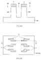
- FIG. 5is a cross-sectional view and a plane view showing a step (removal of the silicon oxide film 12 ) in the method of manufacturing the semiconductor device according to the embodiment of the present invention
- FIG. 6is a cross-sectional view and a plane view showing a step (formation of a trench 15 t ) in the method of manufacturing the semiconductor device according to the embodiment of the present invention
- FIG. 7is a cross-sectional view and a plane view showing a step (formation of an element isolation insulating film 15 ) in the method of manufacturing the semiconductor device according to the embodiment of the present invention
- FIG. 8is a cross-sectional view and a plane view showing a step (formation of a gate insulating film 16 ) in the method of manufacturing the semiconductor device according to the embodiment of the present invention
- FIG. 9is a cross-sectional view and a plane view showing a step (formation of a gate electrode 17 and a cap insulating film 18 (gates 19 )) in the method of manufacturing the semiconductor device according to the embodiment of the present invention.
- FIG. 10is a cross-sectional view and a plane view showing a step (formation of source and drain regions 20 ) in the method of manufacturing the semiconductor device according to the embodiment of the present invention.
- FIG. 11is a cross-sectional view and a plane view showing a step (removal of the gate insulating film 16 on the source and drain regions 20 ) in the method of manufacturing the semiconductor device according to the embodiment of the present invention
- FIG. 12is a cross-sectional view and a plane view showing a step (formation of silicon epitaxial layers 22 ) in the method of manufacturing the semiconductor device according to the embodiment of the present invention
- FIG. 13is a cross-sectional view and a plane view showing a step (formation of an interlayer insulating film 23 and contact plugs 24 ) in the method of manufacturing the semiconductor device according to the embodiment of the present invention
- FIG. 14Ais a general perspective view showing a structure of a conventional fin field effect transistor.
- FIG. 14Bis a general cross-sectional view taken along a line A-A of FIG. 14A .
- FIG. 1With reference to the general perspective view of FIG. 1 , an outline of a fin-FET 10 according to a preferred embodiment of the present invention is described.
- an element isolation insulating film 2is buried in a trench 2 t formed in a semiconductor substrate 1 by a height halfway along a depth of the trench 2 t .
- An active region 4is thereby formed to be surrounded by the trench 2 t and to protrude from an upper surface of the element isolation insulating film 2 .
- the active region 4is crank-shaped and includes a central portion 4 a , a portion 4 b extending from one end of the central portion 4 a in a Y direction, and a portion 4 c extending from the other end of the central portion 4 a in the Y direction.
- An upper surface and side surfaces of each of the central portion 4 a , a part of the portion 4 b , and a part of the portion 4 care covered with a gate electrode 3 .
- a source region and a drain regionare formed in parts of the both side portions 4 b and 4 c of the active region 4 , which parts are not covered with the gate electrode 3 , respectively, by performing ion implantation with the gate electrode 3 used as a mask.
- impurities used in the ion implantationare also diffused into parts of the portions 4 b and 4 c which parts (parts mentioned above) are covered with the gate electrode 4 (implantation lowering).
- the both side portions 4 b and 4 c of the active region 4are connected to the central portion 4 a thereof formed in an X direction in which the gate electrode 3 extends at positions offset to each other in the X direction, respectively. Due to this, the source region and the drain region formed in the respective portions 4 b and 4 c can be distanced from each other, thereby making it possible to suppress the short channel effect. Namely, an effective channel length of the fin-FET 10 is a sum of a width of the gate electrode 3 and an offset width between the portions 4 b and 4 c in the X direction. Therefore, by increasing this offset width, the short channel effect can be sufficiently suppressed accordingly.
- FIG. 2Bis a cross-sectional view taken along a line A-A of FIG. 2A .
- a silicon nitride film 11is formed on a semiconductor substrate 100 .
- the silicon nitride film 11is patterned with a photomask (not shown) used as a mask, thereby leaving the silicon nitride film 11 in the form of a plurality of lands as shown in FIG. 1B .
- a silicon oxide film 12is formed on an entire surface of the semiconductor substrate 100 including portions among and around the lands of the silicon nitride film 11 . Then using the silicon nitride film 11 as a stopper, the silicon oxide film 12 is polished by CMP (Chemical Mechanical Polishing). As a result, the silicon nitride film 11 and the silicon oxide film 12 are flattened so that an upper surface of the silicon nitride film 11 is almost flush with that of the silicon oxide film 12 .
- CMPChemical Mechanical Polishing
- a photoresist 13 including a plurality of openings 14is formed. As shown in FIG. 3B , each of the openings 14 is formed to partially expose the silicon nitride film 11 and the silicon oxide film 12 .
- the silicon nitride film 11 and the silicon oxide film 12are dry etched. As a result, as shown in FIGS. 4A and 4B , the patterned silicon nitride film 11 and the patterned silicon oxide film 12 are left on the semiconductor substrate 100 .
- the silicon oxide film 12is entirely removed by wet etching. As a result, as shown in FIG. 5A , only a plurality of land patterns each made of the silicon nitride film 11 is left on the semiconductor substrate 100 . As shown in FIG. 5B , each of the land patterns is crank-shaped in a plane view.
- the semiconductor substrate 100is dry etched. As a result, as shown in FIG. 6A , a plurality of fin-shaped parts 100 f each defined by trenche 15 t are formed.
- a silicon oxide filmis formed on an entire surface of the semiconductor substrate 100 including interior of the trench 15 t as an element isolation insulating film.
- the element isolation insulating filmis wet etched so that a height of the element isolation insulating film is, for example, about 100 nanometers (nm) from the surface of the semiconductor substrate 100 . Thereafter, the silicon nitride film 11 is removed.
- an element isolation insulating film 15is formed in trench 15 t by a predetermined height.
- Upper portions of the fin-shaped parts 100 fprotrude from an upper surface of the element isolation insulating film 15 . These upper portions serve as active regions 100 a , respectively.
- a pattern of the patterned silicon nitride film 11(see FIG. 6B ) is transferred onto each of the active regions 100 a . Due to this, as shown in FIG. 7B , each of the active regions 100 a is crank-shaped in a plane view. In this manner, the fin-shaped active regions 100 a surrounded by the element isolation insulating film 15 and crank-shaped in a plane view are formed.
- each of the active regions 10 aincludes a central portion fa, a portion fb extending from one end of the central portion fa in the Y direction, and a portion fc extending from the other end thereof in the Y direction.
- the portions fb and fcare arranged to be offset each other in the X direction.
- a gate insulating film 16is formed on a surface of each of the active regions 100 a by performing thermal oxidation.
- a gate electrode film and a silicon nitride filmare formed on the entire surface of the semiconductor substrate 100 , and the gate electrode film and the silicon nitride film are patterned using a photoresist (not shown) having a gate electrode shape.
- a photoresistnot shown
- gates 19each including a gate electrode 17 and a cap insulating film 18 are formed.
- each of the gates 19is formed so as to cover the central portion fa of each of the crank-shaped active regions 100 a covered with the gate insulating film 16 and to cover parts of the portions fb and fc on the respective both sides of the central portion fa (which parts are connected to the central portion fa).
- each of the gates 19 (the cap insulating film 18 and the gate electrode 17 ) and the gate insulating film 16are not hatched so as to show states of the active regions 100 a present under the respective gates 19 .
- ion implantationis performed on the entire surface while using the gates 19 as a mask, thereby forming source and drain regions 20 .
- the ion implantationis performed with high energy so as to implant impurity ions deeply.
- the source and drain regions 20are formed to be diffused even into regions under the gates 19 serving as the mask (implantation lowering).
- the source/drain regions 20 formed on both sides of each of the gates 19are diffused into the region under each gate 19 in each of the active regions 100 a .
- the source region 20 and the drain region 20 formed to put the central portion fa of each of the active regions 100 a between the source region 20 and the drain region 20are located offset each other in the X direction in which the gates 19 extend.
- the portions fb and fc on the both sides of each active region 100 a that portions serve as the source/drain regions 20are arranged on +X side and ⁇ X side in the X direction in which the gates 19 extend, respectively.
- an effective channel length of the fin-FET formed in the embodimentis about a sum of an offset width between the portions fb and fc on the both sides of each active region 100 a and a width of each gate 19 . By making this offset width large, it is possible to sufficiently suppress the short channel effect.
- each of the gates 19 (the cap insulating film 18 and the gate electrode 17 ) and the gate insulating film 16are not hatched so as to show states of the active regions 100 a present under the respective gates 19 .
- sidewall insulating films 21are formed on side surfaces of each of the gates 19 , respectively.
- the sidewall insulating films 21are formed by forming an insulating film for sidewalls on the entire surface of the semiconductor substrate 100 and dry etching (anisotropically etching) the insulating film for sidewalls. Therefore, as shown in FIGS. 11A and 11B , the sidewall insulating films 21 are also formed on sidewalls of portions, which are not covered with the gates 19 (in which portions the source and drain regions 20 are formed), of the active regions 100 a.
- portions, which are not covered with the gates 19 , of the gate insulating film 16 on the source/drain regions 20are selectively removed, thereby exposing surfaces of the source/drain regions 20 as shown in FIGS. 11A and 11B .
- Silicon selective epitaxial growthis then performed.
- siliconis grown only in portions in which silicon is exposed. Due to this, as shown in FIGS. 12A and 12B , silicon epitaxial layers 22 are grown on the exposed portions of the source/drain regions 20 that are a part of the semiconductor substrate 100 .
- the silicon epitaxial layers 22are doped with impurities contained in the source/drain regions 20 during the epitaxial growth. Due to this, the silicon epitaxial layers 22 become conductive layers containing the same impurities as those contained in the source/drain regions 20 .
- the silicon epitaxial layers 22are formed to be wider than the source/drain regions 20 and to run off edges of the active regions 100 a.
- an interlayer insulating film 23is formed on the entire surface of the semiconductor substrate 100 , and contact plugs 24 connected to the respective silicon epitaxial layers 22 are then formed. At this time, since the silicon epitaxial layers 22 are formed wide as stated above, it is possible to secure large positioning margins for the contact plugs 24 .
- each of the active regions 100 ahas a fin structure and each of the gates 19 (gate electrode 17 ) covers the upper and side surfaces of each active region 10 a . Due to this, not only the upper surface but also the side surfaces of each active region 100 a become a channel region, thereby making it possible to ensure a large amount of current.
- the portions, which are covered with the gates 19 , of the active regions 100 ainclude bent portions (a part of each of the portions fb and fc covered with the gates 19 ).
- each active region of the fin-FETare crank-shaped in a plane view.
- the plane shape of each active regionmay be a shape other than the crank shape as long as the shape can suppress the short channel effect.
Landscapes
- Engineering & Computer Science (AREA)
- Manufacturing & Machinery (AREA)
- Insulated Gate Type Field-Effect Transistor (AREA)
- Electrodes Of Semiconductors (AREA)
Abstract
Description
Claims (12)
Applications Claiming Priority (2)
| Application Number | Priority Date | Filing Date | Title |
|---|---|---|---|
| JP2006-233499 | 2006-08-30 | ||
| JP2006233499AJP4487266B2 (en) | 2006-08-30 | 2006-08-30 | Semiconductor device |
Publications (2)
| Publication Number | Publication Date |
|---|---|
| US20080054374A1 US20080054374A1 (en) | 2008-03-06 |
| US7683437B2true US7683437B2 (en) | 2010-03-23 |
Family
ID=39150301
Family Applications (1)
| Application Number | Title | Priority Date | Filing Date |
|---|---|---|---|
| US11/896,050Active2028-02-04US7683437B2 (en) | 2006-08-30 | 2007-08-29 | Semiconductor device having fin field effect transistor and manufacturing method thereof |
Country Status (2)
| Country | Link |
|---|---|
| US (1) | US7683437B2 (en) |
| JP (1) | JP4487266B2 (en) |
Cited By (4)
| Publication number | Priority date | Publication date | Assignee | Title |
|---|---|---|---|---|
| US20110073939A1 (en)* | 2009-09-29 | 2011-03-31 | Elpida Memory, Inc. | Semiconductor device |
| US9601628B2 (en) | 2015-01-15 | 2017-03-21 | Samsung Electronics Co., Ltd. | Semiconductor device having asymmetric fin-shaped pattern |
| US20170278946A1 (en)* | 2015-06-30 | 2017-09-28 | Taiwan Semiconductor Manufacturing Company, Ltd. | Fin semiconductor device and method of manufacture with source/drain regions having opposite conductivities |
| US11152359B2 (en)* | 2019-11-06 | 2021-10-19 | Samsung Electronics Co., Ltd. | Integrated circuit device and a method of manufacturing the same |
Families Citing this family (7)
| Publication number | Priority date | Publication date | Assignee | Title |
|---|---|---|---|---|
| JP2008098553A (en)* | 2006-10-16 | 2008-04-24 | Elpida Memory Inc | Semiconductor device and manufacturing method thereof |
| US8174055B2 (en)* | 2010-02-17 | 2012-05-08 | Globalfoundries Inc. | Formation of FinFET gate spacer |
| US9000525B2 (en) | 2010-05-19 | 2015-04-07 | Taiwan Semiconductor Manufacturing Company, Ltd. | Structure and method for alignment marks |
| KR102352155B1 (en)* | 2015-04-02 | 2022-01-17 | 삼성전자주식회사 | Semiconductor device and method for manufacturing the same |
| WO2017052576A1 (en)* | 2015-09-25 | 2017-03-30 | Intel Corporation | Semiconductor devices including a recessed isolation fill, and methods of making the same |
| JP6713878B2 (en)* | 2016-08-25 | 2020-06-24 | ルネサスエレクトロニクス株式会社 | Method of manufacturing semiconductor device |
| WO2019066768A1 (en)* | 2017-09-26 | 2019-04-04 | Intel Corporation | Directional spacer removal for integrated circuit structures |
Citations (14)
| Publication number | Priority date | Publication date | Assignee | Title |
|---|---|---|---|---|
| JPH05136400A (en) | 1991-10-21 | 1993-06-01 | Samsung Electron Co Ltd | Method for forming contact window of semiconductor device |
| JPH0637279A (en) | 1992-07-17 | 1994-02-10 | Toshiba Corp | Dynamic semiconductor memory device and manufacturing method thereof |
| JPH07122743A (en) | 1993-10-27 | 1995-05-12 | Hitachi Ltd | Semiconductor integrated circuit device and manufacturing method thereof |
| JP2001298194A (en) | 2000-04-14 | 2001-10-26 | Nec Corp | Field effect transistor and manufacturing method thereof |
| JP2002118255A (en) | 2000-07-31 | 2002-04-19 | Toshiba Corp | Semiconductor device and manufacturing method thereof |
| US6664582B2 (en)* | 2002-04-12 | 2003-12-16 | International Business Machines Corporation | Fin memory cell and method of fabrication |
| US20040099885A1 (en)* | 2002-11-26 | 2004-05-27 | Taiwan Semiconductor Manufacturing Co., Ltd. | CMOS SRAM cell configured using multiple-gate transistors |
| WO2004061972A1 (en) | 2002-12-19 | 2004-07-22 | International Business Machines Corporation | Dense dual-plane devices |
| US20040150029A1 (en)* | 2003-02-04 | 2004-08-05 | Lee Jong-Ho | Double-gate FinFET device and fabricating method thereof |
| JP2004281845A (en) | 2003-03-18 | 2004-10-07 | Toshiba Corp | Semiconductor device and method of manufacturing the same |
| US6927458B2 (en)* | 2003-08-08 | 2005-08-09 | Conexant Systems, Inc. | Ballasting MOSFETs using staggered and segmented diffusion regions |
| US20060063334A1 (en) | 2004-09-17 | 2006-03-23 | International Business Machines Corporation | Fin FET diode structures and methods for building |
| JP2006100600A (en) | 2004-09-29 | 2006-04-13 | Toshiba Corp | Semiconductor device and manufacturing method thereof |
| US20070045735A1 (en)* | 2005-08-31 | 2007-03-01 | Orlowski Marius K | FinFET structure with contacts |
Family Cites Families (3)
| Publication number | Priority date | Publication date | Assignee | Title |
|---|---|---|---|---|
| JP2002231826A (en)* | 2001-02-06 | 2002-08-16 | Hitachi Ltd | Semiconductor integrated circuit device |
| KR100702552B1 (en)* | 2003-12-22 | 2007-04-04 | 인터내셔널 비지네스 머신즈 코포레이션 | Automated Layer Creation Method and Device for Double Gate FFT Design |
| JP4504214B2 (en)* | 2005-02-04 | 2010-07-14 | 株式会社東芝 | MOS type semiconductor device and manufacturing method thereof |
- 2006
- 2006-08-30JPJP2006233499Apatent/JP4487266B2/enactiveActive
- 2007
- 2007-08-29USUS11/896,050patent/US7683437B2/enactiveActive
Patent Citations (17)
| Publication number | Priority date | Publication date | Assignee | Title |
|---|---|---|---|---|
| JPH05136400A (en) | 1991-10-21 | 1993-06-01 | Samsung Electron Co Ltd | Method for forming contact window of semiconductor device |
| JPH0637279A (en) | 1992-07-17 | 1994-02-10 | Toshiba Corp | Dynamic semiconductor memory device and manufacturing method thereof |
| JPH07122743A (en) | 1993-10-27 | 1995-05-12 | Hitachi Ltd | Semiconductor integrated circuit device and manufacturing method thereof |
| JP2001298194A (en) | 2000-04-14 | 2001-10-26 | Nec Corp | Field effect transistor and manufacturing method thereof |
| JP2002118255A (en) | 2000-07-31 | 2002-04-19 | Toshiba Corp | Semiconductor device and manufacturing method thereof |
| US6664582B2 (en)* | 2002-04-12 | 2003-12-16 | International Business Machines Corporation | Fin memory cell and method of fabrication |
| US20040099885A1 (en)* | 2002-11-26 | 2004-05-27 | Taiwan Semiconductor Manufacturing Co., Ltd. | CMOS SRAM cell configured using multiple-gate transistors |
| JP2006511962A (en) | 2002-12-19 | 2006-04-06 | インターナショナル・ビジネス・マシーンズ・コーポレーション | High density dual planar device |
| WO2004061972A1 (en) | 2002-12-19 | 2004-07-22 | International Business Machines Corporation | Dense dual-plane devices |
| US6794718B2 (en) | 2002-12-19 | 2004-09-21 | International Business Machines Corporation | High mobility crystalline planes in double-gate CMOS technology |
| US20040150029A1 (en)* | 2003-02-04 | 2004-08-05 | Lee Jong-Ho | Double-gate FinFET device and fabricating method thereof |
| JP2004281845A (en) | 2003-03-18 | 2004-10-07 | Toshiba Corp | Semiconductor device and method of manufacturing the same |
| US6927458B2 (en)* | 2003-08-08 | 2005-08-09 | Conexant Systems, Inc. | Ballasting MOSFETs using staggered and segmented diffusion regions |
| US20060063334A1 (en) | 2004-09-17 | 2006-03-23 | International Business Machines Corporation | Fin FET diode structures and methods for building |
| JP2006086530A (en) | 2004-09-17 | 2006-03-30 | Internatl Business Mach Corp <Ibm> | FINFET diode structure and method of forming the same |
| JP2006100600A (en) | 2004-09-29 | 2006-04-13 | Toshiba Corp | Semiconductor device and manufacturing method thereof |
| US20070045735A1 (en)* | 2005-08-31 | 2007-03-01 | Orlowski Marius K | FinFET structure with contacts |
Non-Patent Citations (1)
| Title |
|---|
| Japanese Office Action dated Nov. 25, 2008 with Partial English-Language Translation. |
Cited By (9)
| Publication number | Priority date | Publication date | Assignee | Title |
|---|---|---|---|---|
| US20110073939A1 (en)* | 2009-09-29 | 2011-03-31 | Elpida Memory, Inc. | Semiconductor device |
| US8633531B2 (en)* | 2009-09-29 | 2014-01-21 | Noriaki Mikasa | Semiconductor device |
| US9601628B2 (en) | 2015-01-15 | 2017-03-21 | Samsung Electronics Co., Ltd. | Semiconductor device having asymmetric fin-shaped pattern |
| US10199377B2 (en) | 2015-01-15 | 2019-02-05 | Samsung Electronics Co., Ltd. | Semiconductor device having asymmetric fin-shaped pattern |
| US10692864B2 (en) | 2015-01-15 | 2020-06-23 | Samsung Electronics Co., Ltd. | Semiconductor device having asymmetric fin-shaped pattern |
| US10910373B2 (en) | 2015-01-15 | 2021-02-02 | Samsung Electronics Co., Ltd. | Semiconductor device having asymmetric fin-shaped pattern |
| US20170278946A1 (en)* | 2015-06-30 | 2017-09-28 | Taiwan Semiconductor Manufacturing Company, Ltd. | Fin semiconductor device and method of manufacture with source/drain regions having opposite conductivities |
| US10269944B2 (en)* | 2015-06-30 | 2019-04-23 | Taiwan Semiconductor Manufacturing Company, Ltd. | Fin semiconductor device and method of manufacture with source/drain regions having opposite conductivities |
| US11152359B2 (en)* | 2019-11-06 | 2021-10-19 | Samsung Electronics Co., Ltd. | Integrated circuit device and a method of manufacturing the same |
Also Published As
| Publication number | Publication date |
|---|---|
| JP4487266B2 (en) | 2010-06-23 |
| JP2008060219A (en) | 2008-03-13 |
| US20080054374A1 (en) | 2008-03-06 |
Similar Documents
| Publication | Publication Date | Title |
|---|---|---|
| US7683437B2 (en) | Semiconductor device having fin field effect transistor and manufacturing method thereof | |
| US9230959B2 (en) | FinFETs having dielectric punch-through stoppers | |
| US6476444B1 (en) | Semiconductor device and method for fabricating the same | |
| KR100618861B1 (en) | A semiconductor device having a local recess channel transistor and a method of manufacturing the same | |
| US7566619B2 (en) | Methods of forming integrated circuit devices having field effect transistors of different types in different device regions | |
| KR100844938B1 (en) | Semiconductor device and manufacturing method thereof | |
| KR100549008B1 (en) | How to manufacture a fin field effect transistor using isotropic etching technology | |
| US20060214212A1 (en) | Semiconductor device and method of manufacturing semiconductor device | |
| US7955913B2 (en) | Method for manufacturing semiconductor device | |
| JP2008300384A (en) | Semiconductor device and manufacturing method thereof | |
| US20110127611A1 (en) | Semiconductor device and method for manufacturing the same | |
| JP2007180486A (en) | 5-channel fin transistor and manufacturing method thereof | |
| JP2008034427A (en) | Semiconductor device and manufacturing method thereof | |
| US7285456B2 (en) | Method of fabricating a fin field effect transistor having a plurality of protruding channels | |
| KR100532204B1 (en) | Transistor having the Fin structure and Method of manufacturing the same | |
| US20080061383A1 (en) | Semiconductor device having fin field effect transistor and manufacturing method thereof | |
| KR100636680B1 (en) | Semiconductor device having recess gate and asymmetric impurity region and manufacturing method thereof | |
| KR100876883B1 (en) | Semiconductor device, manufacturing method thereof and gate forming method of semiconductor device | |
| US7692251B2 (en) | Transistor for semiconductor device and method of forming the same | |
| KR100610421B1 (en) | Manufacturing Method of Semiconductor Device | |
| KR100618904B1 (en) | Semiconductor device including FIFNFT and manufacturing method | |
| JP2003197907A (en) | Transistor structure using epitaxial layer and method of manufacturing the same | |
| KR100558007B1 (en) | Transistor and manufacturing method | |
| US8680612B2 (en) | Semiconductor device and manufacturing method thereof | |
| KR20060130322A (en) | Field effect transistor having vertical channel and manufacturing method thereof |
Legal Events
| Date | Code | Title | Description |
|---|---|---|---|
| AS | Assignment | Owner name:ELPIDA MEMORY, INC.,JAPAN Free format text:ASSIGNMENT OF ASSIGNORS INTEREST;ASSIGNOR:MIKASA, NORIAKI;REEL/FRAME:019800/0082 Effective date:20070801 Owner name:ELPIDA MEMORY, INC., JAPAN Free format text:ASSIGNMENT OF ASSIGNORS INTEREST;ASSIGNOR:MIKASA, NORIAKI;REEL/FRAME:019800/0082 Effective date:20070801 | |
| STCF | Information on status: patent grant | Free format text:PATENTED CASE | |
| FPAY | Fee payment | Year of fee payment:4 | |
| AS | Assignment | Owner name:MICRON TECHNOLOGY, INC., IDAHO Free format text:ASSIGNMENT OF ASSIGNORS INTEREST;ASSIGNOR:ELPIDA MEMORY, INC.;REEL/FRAME:032645/0422 Effective date:20140220 | |
| AS | Assignment | Owner name:U.S. BANK NATIONAL ASSOCIATION, AS COLLATERAL AGENT, CALIFORNIA Free format text:SECURITY INTEREST;ASSIGNOR:MICRON TECHNOLOGY, INC.;REEL/FRAME:038669/0001 Effective date:20160426 Owner name:U.S. BANK NATIONAL ASSOCIATION, AS COLLATERAL AGEN Free format text:SECURITY INTEREST;ASSIGNOR:MICRON TECHNOLOGY, INC.;REEL/FRAME:038669/0001 Effective date:20160426 | |
| AS | Assignment | Owner name:MORGAN STANLEY SENIOR FUNDING, INC., AS COLLATERAL AGENT, MARYLAND Free format text:PATENT SECURITY AGREEMENT;ASSIGNOR:MICRON TECHNOLOGY, INC.;REEL/FRAME:038954/0001 Effective date:20160426 Owner name:MORGAN STANLEY SENIOR FUNDING, INC., AS COLLATERAL Free format text:PATENT SECURITY AGREEMENT;ASSIGNOR:MICRON TECHNOLOGY, INC.;REEL/FRAME:038954/0001 Effective date:20160426 | |
| AS | Assignment | Owner name:U.S. BANK NATIONAL ASSOCIATION, AS COLLATERAL AGENT, CALIFORNIA Free format text:CORRECTIVE ASSIGNMENT TO CORRECT THE REPLACE ERRONEOUSLY FILED PATENT #7358718 WITH THE CORRECT PATENT #7358178 PREVIOUSLY RECORDED ON REEL 038669 FRAME 0001. ASSIGNOR(S) HEREBY CONFIRMS THE SECURITY INTEREST;ASSIGNOR:MICRON TECHNOLOGY, INC.;REEL/FRAME:043079/0001 Effective date:20160426 Owner name:U.S. BANK NATIONAL ASSOCIATION, AS COLLATERAL AGEN Free format text:CORRECTIVE ASSIGNMENT TO CORRECT THE REPLACE ERRONEOUSLY FILED PATENT #7358718 WITH THE CORRECT PATENT #7358178 PREVIOUSLY RECORDED ON REEL 038669 FRAME 0001. ASSIGNOR(S) HEREBY CONFIRMS THE SECURITY INTEREST;ASSIGNOR:MICRON TECHNOLOGY, INC.;REEL/FRAME:043079/0001 Effective date:20160426 | |
| MAFP | Maintenance fee payment | Free format text:PAYMENT OF MAINTENANCE FEE, 8TH YEAR, LARGE ENTITY (ORIGINAL EVENT CODE: M1552) Year of fee payment:8 | |
| AS | Assignment | Owner name:JPMORGAN CHASE BANK, N.A., AS COLLATERAL AGENT, ILLINOIS Free format text:SECURITY INTEREST;ASSIGNORS:MICRON TECHNOLOGY, INC.;MICRON SEMICONDUCTOR PRODUCTS, INC.;REEL/FRAME:047540/0001 Effective date:20180703 Owner name:JPMORGAN CHASE BANK, N.A., AS COLLATERAL AGENT, IL Free format text:SECURITY INTEREST;ASSIGNORS:MICRON TECHNOLOGY, INC.;MICRON SEMICONDUCTOR PRODUCTS, INC.;REEL/FRAME:047540/0001 Effective date:20180703 | |
| AS | Assignment | Owner name:MICRON TECHNOLOGY, INC., IDAHO Free format text:RELEASE BY SECURED PARTY;ASSIGNOR:U.S. BANK NATIONAL ASSOCIATION, AS COLLATERAL AGENT;REEL/FRAME:047243/0001 Effective date:20180629 | |
| AS | Assignment | Owner name:MICRON TECHNOLOGY, INC., IDAHO Free format text:RELEASE BY SECURED PARTY;ASSIGNOR:MORGAN STANLEY SENIOR FUNDING, INC., AS COLLATERAL AGENT;REEL/FRAME:050937/0001 Effective date:20190731 | |
| AS | Assignment | Owner name:MICRON TECHNOLOGY, INC., IDAHO Free format text:RELEASE BY SECURED PARTY;ASSIGNOR:JPMORGAN CHASE BANK, N.A., AS COLLATERAL AGENT;REEL/FRAME:051028/0001 Effective date:20190731 Owner name:MICRON SEMICONDUCTOR PRODUCTS, INC., IDAHO Free format text:RELEASE BY SECURED PARTY;ASSIGNOR:JPMORGAN CHASE BANK, N.A., AS COLLATERAL AGENT;REEL/FRAME:051028/0001 Effective date:20190731 | |
| MAFP | Maintenance fee payment | Free format text:PAYMENT OF MAINTENANCE FEE, 12TH YEAR, LARGE ENTITY (ORIGINAL EVENT CODE: M1553); ENTITY STATUS OF PATENT OWNER: LARGE ENTITY Year of fee payment:12 |