US7682859B2 - Patterned strained semiconductor substrate and device - Google Patents
Patterned strained semiconductor substrate and deviceDownload PDFInfo
- Publication number
- US7682859B2 US7682859B2US11/931,836US93183607AUS7682859B2US 7682859 B2US7682859 B2US 7682859B2US 93183607 AUS93183607 AUS 93183607AUS 7682859 B2US7682859 B2US 7682859B2
- Authority
- US
- United States
- Prior art keywords
- layer
- strained
- substrate
- relaxed
- forming
- Prior art date
- Legal status (The legal status is an assumption and is not a legal conclusion. Google has not performed a legal analysis and makes no representation as to the accuracy of the status listed.)
- Expired - Lifetime
Links
- 239000000758substrateSubstances0.000titleclaimsabstractdescription100
- 239000004065semiconductorSubstances0.000titleclaimsdescription15
- 239000000463materialSubstances0.000claimsabstractdescription195
- 238000000034methodMethods0.000claimsabstractdescription54
- 229910000577Silicon-germaniumInorganic materials0.000claimsabstractdescription33
- LEVVHYCKPQWKOP-UHFFFAOYSA-N[Si].[Ge]Chemical compound[Si].[Ge]LEVVHYCKPQWKOP-UHFFFAOYSA-N0.000claimsabstractdescription6
- HMDDXIMCDZRSNE-UHFFFAOYSA-N[C].[Si]Chemical compound[C].[Si]HMDDXIMCDZRSNE-UHFFFAOYSA-N0.000claimsabstractdescription4
- 239000011810insulating materialSubstances0.000claimsdescription9
- 238000005530etchingMethods0.000claimsdescription7
- 238000000151depositionMethods0.000claimsdescription6
- 150000004767nitridesChemical class0.000claimsdescription4
- 229910052732germaniumInorganic materials0.000claimsdescription3
- GNPVGFCGXDBREM-UHFFFAOYSA-Ngermanium atomChemical compound[Ge]GNPVGFCGXDBREM-UHFFFAOYSA-N0.000claimsdescription2
- OKTJSMMVPCPJKN-UHFFFAOYSA-NCarbonChemical compound[C]OKTJSMMVPCPJKN-UHFFFAOYSA-N0.000claims1
- 229910052799carbonInorganic materials0.000claims1
- 239000011248coating agentSubstances0.000claims1
- 238000000576coating methodMethods0.000claims1
- 229910052710siliconInorganic materials0.000abstractdescription58
- XUIMIQQOPSSXEZ-UHFFFAOYSA-NSiliconChemical compound[Si]XUIMIQQOPSSXEZ-UHFFFAOYSA-N0.000abstractdescription57
- 239000010703siliconSubstances0.000abstractdescription57
- 238000004519manufacturing processMethods0.000description28
- 230000015572biosynthetic processEffects0.000description18
- 230000007547defectEffects0.000description15
- 230000008569processEffects0.000description14
- HBMJWWWQQXIZIP-UHFFFAOYSA-Nsilicon carbideChemical compound[Si+]#[C-]HBMJWWWQQXIZIP-UHFFFAOYSA-N0.000description10
- 229910010271silicon carbideInorganic materials0.000description9
- 238000001020plasma etchingMethods0.000description7
- 230000008021depositionEffects0.000description4
- 238000005229chemical vapour depositionMethods0.000description3
- 238000005259measurementMethods0.000description3
- 238000000038ultrahigh vacuum chemical vapour depositionMethods0.000description3
- 229910052581Si3N4Inorganic materials0.000description2
- 239000003990capacitorSubstances0.000description2
- 150000001875compoundsChemical class0.000description2
- 238000007796conventional methodMethods0.000description2
- 238000001312dry etchingMethods0.000description2
- 239000012212insulatorSubstances0.000description2
- 238000004518low pressure chemical vapour depositionMethods0.000description2
- 238000000059patterningMethods0.000description2
- 238000012545processingMethods0.000description2
- 238000001289rapid thermal chemical vapour depositionMethods0.000description2
- HQVNEWCFYHHQES-UHFFFAOYSA-Nsilicon nitrideChemical compoundN12[Si]34N5[Si]62N3[Si]51N64HQVNEWCFYHHQES-UHFFFAOYSA-N0.000description2
- 239000000126substanceSubstances0.000description2
- JBRZTFJDHDCESZ-UHFFFAOYSA-NAsGaChemical compound[As]#[Ga]JBRZTFJDHDCESZ-UHFFFAOYSA-N0.000description1
- GYHNNYVSQQEPJS-UHFFFAOYSA-NGalliumChemical compound[Ga]GYHNNYVSQQEPJS-UHFFFAOYSA-N0.000description1
- UFHFLCQGNIYNRP-UHFFFAOYSA-NHydrogenChemical compound[H][H]UFHFLCQGNIYNRP-UHFFFAOYSA-N0.000description1
- 206010023204Joint dislocationDiseases0.000description1
- OAICVXFJPJFONN-UHFFFAOYSA-NPhosphorusChemical compound[P]OAICVXFJPJFONN-UHFFFAOYSA-N0.000description1
- VYPSYNLAJGMNEJ-UHFFFAOYSA-NSilicium dioxideChemical compoundO=[Si]=OVYPSYNLAJGMNEJ-UHFFFAOYSA-N0.000description1
- 238000013459approachMethods0.000description1
- 230000001174ascending effectEffects0.000description1
- 238000006243chemical reactionMethods0.000description1
- 239000007795chemical reaction productSubstances0.000description1
- 230000006835compressionEffects0.000description1
- 238000007906compressionMethods0.000description1
- 230000001010compromised effectEffects0.000description1
- 230000003247decreasing effectEffects0.000description1
- 230000002950deficientEffects0.000description1
- 238000000866electrolytic etchingMethods0.000description1
- 230000008030eliminationEffects0.000description1
- 238000003379elimination reactionMethods0.000description1
- 238000005516engineering processMethods0.000description1
- -1for exampleSubstances0.000description1
- 229910052733galliumInorganic materials0.000description1
- 229910052739hydrogenInorganic materials0.000description1
- 239000001257hydrogenSubstances0.000description1
- 239000007788liquidSubstances0.000description1
- 238000004377microelectronicMethods0.000description1
- 238000012986modificationMethods0.000description1
- 230000004048modificationEffects0.000description1
- 238000001451molecular beam epitaxyMethods0.000description1
- 230000006911nucleationEffects0.000description1
- 238000010899nucleationMethods0.000description1
- 239000002245particleSubstances0.000description1
- 229910052698phosphorusInorganic materials0.000description1
- 239000011574phosphorusSubstances0.000description1
- 238000005498polishingMethods0.000description1
- 230000009467reductionEffects0.000description1
- 229910052814silicon oxideInorganic materials0.000description1
- 239000007787solidSubstances0.000description1
- 238000000992sputter etchingMethods0.000description1
Images


Classifications
- H—ELECTRICITY
- H10—SEMICONDUCTOR DEVICES; ELECTRIC SOLID-STATE DEVICES NOT OTHERWISE PROVIDED FOR
- H10D—INORGANIC ELECTRIC SEMICONDUCTOR DEVICES
- H10D30/00—Field-effect transistors [FET]
- H10D30/60—Insulated-gate field-effect transistors [IGFET]
- H10D30/751—Insulated-gate field-effect transistors [IGFET] having composition variations in the channel regions
- H—ELECTRICITY
- H10—SEMICONDUCTOR DEVICES; ELECTRIC SOLID-STATE DEVICES NOT OTHERWISE PROVIDED FOR
- H10D—INORGANIC ELECTRIC SEMICONDUCTOR DEVICES
- H10D12/00—Bipolar devices controlled by the field effect, e.g. insulated-gate bipolar transistors [IGBT]
- H—ELECTRICITY
- H10—SEMICONDUCTOR DEVICES; ELECTRIC SOLID-STATE DEVICES NOT OTHERWISE PROVIDED FOR
- H10D—INORGANIC ELECTRIC SEMICONDUCTOR DEVICES
- H10D30/00—Field-effect transistors [FET]
- H10D30/60—Insulated-gate field-effect transistors [IGFET]
- H10D30/67—Thin-film transistors [TFT]
- H10D30/674—Thin-film transistors [TFT] characterised by the active materials
- H10D30/6741—Group IV materials, e.g. germanium or silicon carbide
- H10D30/6748—Group IV materials, e.g. germanium or silicon carbide having a multilayer structure or superlattice structure
- H—ELECTRICITY
- H10—SEMICONDUCTOR DEVICES; ELECTRIC SOLID-STATE DEVICES NOT OTHERWISE PROVIDED FOR
- H10D—INORGANIC ELECTRIC SEMICONDUCTOR DEVICES
- H10D84/00—Integrated devices formed in or on semiconductor substrates that comprise only semiconducting layers, e.g. on Si wafers or on GaAs-on-Si wafers
- H10D84/01—Manufacture or treatment
- H10D84/0123—Integrating together multiple components covered by H10D12/00 or H10D30/00, e.g. integrating multiple IGBTs
- H10D84/0126—Integrating together multiple components covered by H10D12/00 or H10D30/00, e.g. integrating multiple IGBTs the components including insulated gates, e.g. IGFETs
- H10D84/0128—Manufacturing their channels
- H—ELECTRICITY
- H10—SEMICONDUCTOR DEVICES; ELECTRIC SOLID-STATE DEVICES NOT OTHERWISE PROVIDED FOR
- H10D—INORGANIC ELECTRIC SEMICONDUCTOR DEVICES
- H10D84/00—Integrated devices formed in or on semiconductor substrates that comprise only semiconducting layers, e.g. on Si wafers or on GaAs-on-Si wafers
- H10D84/01—Manufacture or treatment
- H10D84/02—Manufacture or treatment characterised by using material-based technologies
- H10D84/03—Manufacture or treatment characterised by using material-based technologies using Group IV technology, e.g. silicon technology or silicon-carbide [SiC] technology
- H10D84/038—Manufacture or treatment characterised by using material-based technologies using Group IV technology, e.g. silicon technology or silicon-carbide [SiC] technology using silicon technology, e.g. SiGe
Definitions
- eDRAMembedded Dynamic Random Access Memory
- ASICApplication Specific Integrated Circuits
- SoCsystem-on-chip
- logic devicesexhibit better performance when formed on a tensily strained silicon layer that is epitaxially grown on another epitaxially grown silicon germanium (SiGe) layer that has been relaxed.
- a fully relaxed SiGe layerhas a lattice constant which is larger than that of silicon.
- the silicon layerconforms to the larger lattice constant of the relaxed SiGe layer and this applies physical biaxial stress to the silicon layer being formed thereon. This physical biaxial stress applied to the silicon layer increases the performance of logic devices formed in the strained silicon.
- SiGe on silicon substratesrelaxation in SiGe on silicon substrates occurs through the formation of misfit dislocations, which when equally spaced to relieve stress cause the substrate to be perfectly relaxed. Additionally, the misfit dislocations provide extra half-planes of silicon in the substrate. This allows the lattice constant in the SiGe layer to seek its intrinsic value. In this manner, the SiGe lattice constant grows larger as the mismatch strain across the SiGe/silicon interface is accommodated.
- the problem with this approachis that it requires a very thick, multilayered SiGe layer. Additionally, the misfit dis-locations formed between the SiGe layer and the epitaxial silicon layer are random, highly non-uniform in density, and fairly uncontrollable due to heterogeneous nucleation that cannot be easily controlled. Consequently, the physical stress applied to the silicon layer is apt to be defective. At locations where misfit density is high, defects form in the strained silicon layer. These defects short device terminals and cause other leakage problems. For this reason, although the performance of logic devices is strengthened when the logic devices are formed in areas of strained silicon, the performance of defect-sensitive devices such as DRAM devices degrades when formed therein. The production yield is also compromised when the defect-sensitive devices are formed in the strained regions.
- the electrical deviceincludes a buffer layer formed in contact with a portion of a substrate.
- the buffer layerhas a lattice constant/structure mismatch with the substrate.
- the devicefurther includes a relaxed layer formed on the buffer layer.
- the devicealso includes a strained material formed on a top surface of the relaxed layer. The relaxed layer places the strained material in one of a tensile or a compressive state.
- the devicestill further includes a non-strained material patterned proximate the strained material.
- FIG. 11shows a final structure of an electrical device according to a second embodiment of the invention.
- FIGS. 12-15show fabricating steps of manufacturing an electrical device according to a third embodiment of the invention.
- FIG. 16shows a final structure of an electrical device according to a third embodiment of the invention.
- FIG. 33is a cross-sectional view of an electrical device according to a seventh embodiment of the invention that is formed using a combination of the methods and materials shown in FIGS. 1-32 ;
- FIG. 34is a flowchart representing fabricating steps of manufacturing the electrical device shown in FIGS. 1-5 ;
- FIG. 35is a flowchart representing fabricating steps of manufacturing the electrical device shown in FIGS. 6-11 ;
- FIG. 36is a flowchart representing fabricating steps of manufacturing the electrical device shown in FIGS. 12-16 ;
- FIG. 37is a flowchart representing fabricating steps of manufacturing the electrical device shown in FIGS. 17-22 ;
- FIG. 38is a flowchart representing fabricating steps of manufacturing the electrical device shown in FIGS. 23-27 ;
- FIG. 39is a flowchart representing fabricating steps of manufacturing the electrical device shown in FIGS. 28-32 .
- the inventionis directed to an electrical, digital, semiconductor, or other device having a substrate on which a pattern of strained and non-strained (i.e., relaxed) materials are formed.
- the strained materialmay be placed in tension or compression due to a lattice constant/structure difference with an underlying layer of relaxed material.
- the relaxed materialis formed on a buffer layer, which contacts a portion of the substrate.
- a material forming the buffer layervaries in concentration throughout the layer, and has a lattice constant/structure mismatch with the material that forms the substrate. Because the material forming the buffer layer increases in concentration the further the buffer layer extends from the substrate, defects normally caused by the lattice mis-match are virtually eliminated.
- the formation of the relaxed layer on the buffer layerfurther reduces and/or eliminates defects to such an extent that the strained material is virtually free of defects.
- the drastic reduction or elimination of defects in the strained materialallows electronic or digital devices formed therein to operate very fast and very efficiently. It also allows devices such as Dynamic Random Access Memory (DRAM) to be formed in an adjacent relaxed material because such devices are normally very sensitive to defects.
- DRAMDynamic Random Access Memory
- Electroderefers to an electrical, electro-mechanical, semiconductor, digital, or similar device.
- Illustrative types of electrical devicesinclude, but are not limited to, transistors, capacitors, resistors, logic devices, memory devices, computer processors, traces, vias, semi-conductor wafer, computer chip, application specific integrated circuit (ASIC), system-on-chip (SoC), and the like.
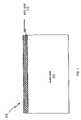
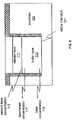
- the electrical device 100includes a substrate 101 covered with a pad layer 103 .
- the substratehas a semiconductor-on-insulator type structure, e.g., a silicon-on-insulator (SOI) substrate.
- SOIsilicon-on-insulator
- the thickness of the substrateapproximates that of a standard semiconductor wafer known in the art.
- the material forming the pad layer 103will vary depending on the type of manufacturing process used.
- Exemplary pad layer materialsinclude, but are not limited to, silicon nitride and/or silicon oxide. Persons skilled in the art, however, will readily understand additional types of materials that can be used to form the pad layer.
- the pad layerhas an overall thickness of about 0.2 microns when it is desired to form a recess that is approximately 2.0 micron deep. This exemplary thickness may be applied to all embodiments herein described.
- the substrate 101is shown having a recess 105 formed therein formed using reactive ion etching or dry etching processes.
- the exact width of recess 105is not critical, but the depth is formed in the range of about 1.0 micron to about 3.0 microns deep. An exemplary width is about 100 microns.
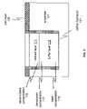
- an insulating layer 107 formed of an oxide or nitride materialis conformally deposited on the sidewalls and bottom 109 of the recess 105 using any suitable deposition or growth process known in the art.
- the insulating layeris formed to be in the range of approximately 10 Angstroms to about 100 Angstroms thick.
- This exemplary measurementmay be applied to all embodiments described herein.
- lateral, but not vertical, portions thereofare removed from the recess using anisotropic etching such as reactive ion etching (RIE). That is, the portion of the insulating layer 107 formed on the recess bottom 109 is removed; however the insulating layer formed on the recess sidewalls remains thereon.
- RIEreactive ion etching
- the insulating layer 107is also formed on the interior exposed edges of the pad layer, as shown.
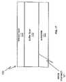
- a buffer layer 113forms a lattice constant/structure mismatch 121 with the substrate 101 and functions to constrain most of the dislocations caused by the mismatch.
- the buffer layermay have an overall thickness from less than about 0.5 microns to more than about 2.0 microns.
- a relaxed layer 111is formed on the buffer layer and remains relatively defect free.
- the overall thickness of the relaxed layer 111may be about 0.2 microns.
- the buffer layer 113 and the relaxed layer 111are epitaxially grown in the recess 105 , within the confines of the insulating layer 107 .
- Buffer layer 113is formed first, then the relaxed layer 111 .
- the buffer layer 113 growth processstarts from the recess bottom 109 and works upwards, layer after layer, until an overall thickness of approximately 0.5 micron to approximately 2.0 micron is reached.
- silicon germanium (SiGe)is used to form the buffer layer 113 and the relaxed layer 111 in order to subsequently form a semiconductor layer such as silicon atop of the relaxed layer 111 with a tensile stress.
- silicon carbon (SiC)may be used to provide a compressive strain in the subsequently formed silicon layer.
- the buffer layer 113 and the relaxed layer 111may be deposited or grown using conventional techniques such as chemical vapor deposition methods.
- UHVCVDultrahigh vacuum chemical vapor deposition
- Other conventional techniquesinclude rapid thermal chemical vapor deposition (RTCVD), low pressure chemical vapor deposition (LPCVD), limited reaction processing CVD (LRPCVD) and molecular beam epitaxy (MBE).
- RTCVDrapid thermal chemical vapor deposition
- LPCVDlow pressure chemical vapor deposition
- LPCVDlimited reaction processing CVD
- MBEmolecular beam epitaxy
- a thin silicon buffer layer(not shown) may be formed on the interior walls of the recess 105 before SiGe or SiC formation.
- the multi-layered buffer layer 113is constructed in such a fashion that a concentration of a material (Ge, for example) incrementally increases from a base concentration 119 proximate the bottom of the recess to a benchmark concentration 117 proximate a top surface of the buffer layer.
- This incremental increase in concentrationmay be in any stepped fashion, such as for example, by 10% for each new deposition or grown layer. However, any percentage increase may be used depending on the desired applications and requested costs.
- the concentration of Gecan range from a base concentration of less than about 1% to a benchmark concentration of 100%. However, for cost and other reasons, a benchmark concentration of about 40% may be used.
- the second base concentration 115 of a material used to form the relaxed layer 111i.e., Ge if SiGe is used
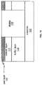
- the pad layeris removed, and a layer of material (such as, but not limited to, Si) is epitaxially grown within and without the confines of the insulating layer 107 to formed relaxed material 123 and strained material 125 .
- Material 123is described as relaxed (or non-strained) because its lattice constant approximately equals the lattice constant of the substrate 101 .
- Material 125is described as strained because its lattice constant differs from the lattice constant of a material used to form the relaxed layer 111 . Consequently, a lattice mismatch 127 occurs at the interface between the strained material 125 and the buffer layer 113 .
- strained material 125may be placed in one of a tensile or a compressive state.
- strained material 125is tensily strained when it is formed of Si and the relaxed layer is formed of SiGe.
- the strained material 125is compressively strained when it is formed of Si and the relaxed layer 111 is formed of SiC.
- any two different semiconductor materialsmay be used, because the different lattice structure/constants of each material will exert either a compressive or tensile strain.
- the strained material 125 and the relaxed material 123each have an overall thickness from less than about 20 nanometers to more than about 100 nanometers. These exemplary thicknesses may be used in various embodiments herein described.
- FIGS. 6-11Alternate embodiments and methods of manufacture will now be described with reference to FIGS. 6-11 . Because the materials, etching methods, epitaxial growth methods, and deposition methods used to form the embodiments of FIGS. 6-11 are the same as those described above, these figures will be described in less detail in order not to unnecessarily obscure aspects of the invention.
- FIG. 6a cross-section of an electrical device 100 is shown.
- the device 100includes a substrate 101 covered by a pad layer 103 .
- a recess 105is etched through the pad layer 103 and into the substrate 101 to a pre-determined depth, as described above.
- an oxide or nitride insulating layer 107is conformally coated on the interior of the recess 105 .
- the bottom portion of the insulating layer 107is then removed, leaving the portions adhered to the recess sidewalls virtually intact.
- FIG. 8depicts the formation of the buffer layer 113 and the relaxed layer 111 in the recess 105 , within the confines of the insulating layer 107 .
- a material forming the buffer layervaries in concentration from a base concentration 119 to a benchmark concentration 117 .
- a second base concentration 115 of a material forming the relaxed layer 111is chosen to approximately match the benchmark concentration 117 of the buffer layer 113 .
- the buffer layer 113functions to contain dislocations caused by the lattice mismatch 121 .
- FIG. 9illustrates the discrete and selective formation of a strained material 125 in the recess 105 , within the confines of the insulating layer 107 , and on top of the relaxed layer 111 .
- the type of material used to form the relaxed layer 111determines whether a tensile or compressive force is applied to the strained material 125 .
- FIG. 10depicts removal of the pad layer 103 and subsequent planarization of the substrate 101 .
- This Figurealso illustrates the lattice mismatch 127 between the strained material 125 and the relaxed layer 111 .
- the type of process used to remove the pad layerdepends on the type of material used to form such layers. For example, if silicon nitride is used as the pad layer, then a wet etch using hot phosphoric (H 3 PO 4 ) may be used.
- the type of planarization method usedmay be any suitable planarization technique. For example, in one embodiment, chemical mechanical polishing (CMP) may be used. In another embodiment, a high temperature reflow process with the presence of hydrogen may be used.
- CMPchemical mechanical polishing
- a high temperature reflow process with the presence of hydrogenmay be used.
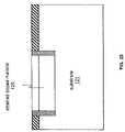
- FIG. 11shows the formation of electrical devices 129 and 131 in the strained material 125 and in the non-strained regions of the substrate 101 .
- portions of the substrate 101 that are outside the confines of the insulating layer 107form the relaxed material 123 shown in FIG. 4 .
- FIG. 12illustrates a cross-sectional view of an electrical device 100 (i.e., a silicon wafer), which includes a substrate 101 on which are formed, in ascending order, buffer layer 113 , relaxed layer 111 , and strained material 125 .
- This Figurealso illustrates the lattice mismatch 121 formed between the substrate 101 and a lower surface of the buffer layer 113 , and the lattice mismatch 127 formed between the relaxed layer 111 and the strained material 125 .
- These layerscan be grown or deposited in any known manner, with the buffer layer 113 having, in one embodiment, a higher concentration of material closest to the strained layer and gradually decreasing in concentration. This will eliminate or reduce formation of defects in the end product.
- FIG. 13depicts the formation of a recess 105 that extends through the pad layer 103 , the strained material 125 , the relaxed layer 111 , and the buffer layer 113 , but which has as its bottom a portion of the top surface of the substrate 101 .
- strained device 129is located outside the confines of the insulating material, and the non-strained device is located within those confines.
- a fourth embodimentis shown with respect to FIGS. 17 22 .
- a cross-sectional view of an electrical device 100 in accordance with the fourth embodimentis shown in FIG. 17 .
- the device 100includes a substrate 101 on which a buffer layer 113 of SiGe is formed. In an alternate embodiment, SiC can also be formed.
- a relaxed layer 111also formed of SiGe (or alternatively SiC), covers the top surface of the buffer layer.
- the lattice mismatch 121 between the buffer layer and the silicon substrate 101is in the illustrative range of 2% or less. This means that the lattice constant of the lowest SiGe buffer layer differs from the lattice constant of the silicon substrate by about 2% or less. This same percentage may also be applicable for any of the embodiments disclosed herein.
- FIG. 18illustrates the formation of a recess 105 that extends through the pad layer 103 , through the relaxed layer 111 , and through the buffer layer 113 to expose a top surface of the silicon substrate 101 .
- FIG. 19depicts the formation of an insulating layer 107 on the sidewalls of the recess 105 and the formation of the relaxed material 123 in the recess, as previously described.
- the pad layerhas been removed, and the top surface of relaxed layer 111 , insulating layer 107 , and relaxed material 123 have been planarized. Thereafter, as shown in FIG. 21 , a layer of silicon is epitaxially grown to cover the entire planarized surface.
- the lattice mismatch between the relaxed layer and the silicon layerplaces a tensile or compressive strain on the silicon, thereby creating strained material 125 .
- a relaxed (non-strained material) 124is created within the confines of the recess 105 .
- the insulating layer 107does not separate the strained material 125 from the second relaxed material 124 , the lateral strain between the strained material 125 and non-strained materials 124 is minimal compared to the strain imposed by the strain imposed by the relaxed layer 111 .
- FIG. 22illustrates the formation of a strained device 129 in the strained material 125 , and the formation of a non-strained device 131 in the relaxed material 124 .
- the strained device 129may be a logic device, and the non-strained device may be a DRAM.
- other electrical devicessuch as transistors and capacitors, may also be used.
- FIGS. 23-27are cross-sectional views of an electrical device 100 that illustrate the formation of a strained material 125 using doped silicon on a substrate 101 .
- a pad layer 103is formed on a silicon substrate 101 .
- a recess 105is etched through the pad layer and into the substrate 101 to an exemplary depth of approximately 0.05 or 1 microns, as measured from a top surface of the substrate 101 .
- an optional insulating layer 107formed of an oxide or a nitride material, is formed on the sidewalls of and bottom of the recess 105 using chemical vapor deposition or other known processes.
- FIG. 26shows that the pad layer 103 has been etched away using either a dry or wet etch, as previously described, and that the top surface of the substrate 101 is planarized to be approximately level with the top surfaces of strained material 125 , insulating layer 107 and the substrate 101 .
- strained material 125is selectively formed in the recess 105 and separated from the non-strained areas 126 of the substrate 101 by the insulating layer 107 .
- a strained device 129such as a logic device, is formed in the strained material 125 ; and a non-strained device 131 is formed in the non strained area 126 of the substrate 101 .
- FIGS. 28-32are cross-sectional views of an electrical device 100 that illustrate another formation of a strained material 125 using doped silicon on a silicon substrate 101 .
- a silicon substrate 101is prepared for processing.
- a carbon-doped strained material 125is epitaxially grown on a top surface of the substrate 101 .
- the strained layer 125has a thickness less than the so-called “critical thickness”. The critical thickness is defined as the maximum thick of the strained layer below which there is virtually no defects is generated.
- the strained material 125is carbon-doped silicon.
- a compressive-strained layermay be formed by forming a germanium-doped silicon layer on silicon substrate.
- a patterned pad layer 103is formed on the strained material 125 . Areas of the non-strained silicon substrate are exposed by using an etching process to remove areas of strained doped material 125 that are not covered by the pad layer 103 .
- a non-strained (relaxed) material 123is epitaxially grown on the exposed areas of the substrate 101 to approximately the same height of the strained layer 125 to form a substantially planar top surface.
- Epitaxially growing the non-strained material 123is optional, since the strained material 125 , in this embodiment, is very thin (e.g., less than about 100 nanometers).
- the pad layer 103is etched away and a strained device 129 is formed in the strained material 125 .
- a non-strained device 131is formed in the relaxed material 123 .
- FIG. 33is a cross-sectional view illustrating an electrical device 100 having tensile-strained, compressive-strained, and non-strained materials 123 , 124 , and 123 , respectively. As shown, each of these materials is formed on a surface of a substrate 101 using any combination of the techniques discussed above. The lateral strain experienced at junctions 133 is minimal compared to the vertical strain exerted by the lattice mismatches 127 A and 127 B, respectively. Alternatively, these layers may also be separated by insulating materials.
- the tensile strained material 125 Ais a carbon-doped silicon layer formed on silicon and the compressive strained material 125 B is a germanium-doped silicon layer formed on silicon.
- the tensile strained material 125 Ais a silicon layer formed on the SiGe buffer layer(s) (not shown) and the compressive strained material 125 B is a silicon layer formed on SiC buffer layer(s) (not shown).
- the relaxed material 123may also be a relaxed top surface of the substrate 101 , as previously illustrated and described with reference to FIGS. 31 and 32 . Although illustratively shown that these layers have the same thickness, their thicknesses may not necessary be the same.
- FIGS. 1-33can equally represent methods of manufacture.
- FIGS. 34-39show various methods for manufacturing the apparatus according to various aspects of the invention. Although herein described with reference to sequential reference numerals, the steps of each method may be performed in any order. The removing of layers to form a recess, forming layers and other processes may be provided by any known method of fabrication. For example, illustrative manufacturing processes include, but are not limited to, chemical vapor deposition, ultra-high vacuum chemical vapor deposition, and reactive ion etching (RIE), electrolytic etching, plasma etching, dry etching, and the like.
- RIEreactive ion etching
- Ion etchingis a process of removing unwanted material by selectively bombarding an area or areas of a solid or liquid substance with energetic ionized particles. Often used in the manufacture of microelectronics, plasma etching creates reactive species in a plasma and then uses the reactive species to selectively remove unwanted material.
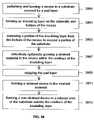
- FIG. 34is a flowchart illustrating an exemplary method of manufacturing an electrical device 100 , according to one embodiment of the invention.
- a recessis patterned and formed in a substrate covered by a pad layer.
- an insulating layeris optionally formed on the sidewalls and bottom of the recess.
- a portion of the insulating layeris removed from the bottom of the recess to expose a portion of the substrate.
- a buffer layeris formed in the recess within the confines of the insulating layer, the buffer layer having a lattice constant/structure mismatch with the substrate.
- the concentration of a material forming the buffer layeris increased as the buffer layer is formed from a base concentration to a benchmark concentration.
- a relaxed layeris formed on the buffer layer.
- the pad layeris stripped.
- a strained materialis formed on the relaxed layer within the confines of the insulating layer, and a non-strained material is formed on a portion of the substrate outside the confines of the insulating layer.
- a strained deviceis formed in the strained material.
- a non-strained deviceis formed in the relaxed material.
- a material forming the relaxed layerhas a second base concentration proximate a bottom surface thereof that approximately equals the benchmark concentration proximate a top surface of the buffer layer.
- FIG. 35is a flowchart illustrating an exemplary method of manufacturing an electrical device 100 , according to one embodiment of the invention.
- a recessis patterned and formed in a substrate covered by a pad layer.
- an insulating layeris formed on the sidewalls and bottom of the recess.
- a portion of the insulating layeris removed from the bottom of the recess to expose a portion of the substrate.
- a buffer layeris formed in the recess within the confines of the insulating layer, the buffer layer having a lattice constant/structure mismatch with the substrate.
- the concentration of a material forming the buffer layeris increased as the buffer layer is formed, from a base concentration to a benchmark concentration.
- a relaxed layeris formed on the buffer layer.
- a strained materialis formed on the relaxed layer in the recess within the confines of the insulating layer.
- the pad layeris stripped.
- the substrateis planarized.
- a strained deviceis formed in the strained material.
- a non-strained deviceis formed in the relaxed material.
- a material forming the relaxed layerhas a second base concentration proximate a bottom surface thereof that approximately equals the benchmark concentration proximate a top surface of the buffer layer.
- FIG. 36is a flowchart illustrating an exemplary method of manufacturing an electrical device 100 , according to one embodiment of the invention.
- a pad layeris formed on a strained material.
- a recessis patterned and formed through the strained material, through a relaxed layer previously formed proximate thereto, and through a buffer layer previously formed proximate to the relaxed layer and in contact with a substrate.
- an insulating layeris formed on the sidewalls and bottom of the recess.
- the insulating layeris removed from the bottom of the recess.
- a relaxed materialis formed in the recess within the confines of the insulating material.
- the pad layeris stripped.
- the substrateis planarized.
- a strained deviceis formed in the strained material.
- a non-strained deviceis formed in the relaxed material.
- a strained materialis formed on the relaxed layer outside the confines of the insulating layer.
- a relaxed materialis formed in the recess within the confines of the insulating layer.
- a strained deviceis formed in the strained material.
- a non-strained deviceis formed in the relaxed material.
- FIG. 38is a flowchart illustrating an exemplary method of manufacturing an electrical device 100 , according to one embodiment of the invention.
- a recessis patterned and formed in a substrate covered by a pad layer.
- an insulating layeris formed on the sidewalls and bottom of the recess.
- a strained materialis selectively and epitaxially grown in the recess within the confines of the insulating layer.
- the pad layeris stripped.
- a strained deviceis formed in the strained material.
- a non-strained deviceis formed in a relaxed area of the substrate outside the confines of the insulating layer.
- the strained materialmay be a carbon-doped material, such as, but not limited to, carbon-doped silicon.
- the strained materialmay be a germanium-doped material, such as, not limited to, germanium-doped silicon.
- FIGS. 1-22Although embodiments of the invention have been illustrated in FIGS. 1-22 as fusing SiGe to form a tensile-strained material 125 , it will be appreciated that other materials, such as SiC, may be substituted for SiGe, where it is desired to form a compressive-strained material 125 . Additionally, a tensile-strained material 125 may be formed by epitaxially growing carbon-doped silicon on a silicon substrate. Other materials such as gallium phosphorus, gallium arsenic and the like, may also be substituted for SiGe, depending on desired applications and requested costs.
- an electrical device formed in accordance with an embodiment of the inventionmay have a non-strained (relaxed) material 123 , 124 , 126 patterned proximate a strained material 125 , 125 A and 125 B, as illustratively shown and described with respect to FIGS. 4 , 15 , 21 , 26 , 31 and 33 .
Landscapes
- Recrystallisation Techniques (AREA)
- Thin Film Transistor (AREA)
- Insulated Gate Type Field-Effect Transistor (AREA)
- Metal-Oxide And Bipolar Metal-Oxide Semiconductor Integrated Circuits (AREA)
- Pressure Sensors (AREA)
Abstract
Description
Claims (18)
Priority Applications (2)
| Application Number | Priority Date | Filing Date | Title |
|---|---|---|---|
| US11/931,836US7682859B2 (en) | 2004-07-23 | 2007-10-31 | Patterned strained semiconductor substrate and device |
| US12/686,040US9053970B2 (en) | 2004-07-23 | 2010-01-12 | Patterned strained semiconductor substrate and device |
Applications Claiming Priority (2)
| Application Number | Priority Date | Filing Date | Title |
|---|---|---|---|
| US10/710,608US7384829B2 (en) | 2004-07-23 | 2004-07-23 | Patterned strained semiconductor substrate and device |
| US11/931,836US7682859B2 (en) | 2004-07-23 | 2007-10-31 | Patterned strained semiconductor substrate and device |
Related Parent Applications (1)
| Application Number | Title | Priority Date | Filing Date |
|---|---|---|---|
| US10/710,608DivisionUS7384829B2 (en) | 2004-07-23 | 2004-07-23 | Patterned strained semiconductor substrate and device |
Related Child Applications (1)
| Application Number | Title | Priority Date | Filing Date |
|---|---|---|---|
| US12/686,040DivisionUS9053970B2 (en) | 2004-07-23 | 2010-01-12 | Patterned strained semiconductor substrate and device |
Publications (2)
| Publication Number | Publication Date |
|---|---|
| US20080061317A1 US20080061317A1 (en) | 2008-03-13 |
| US7682859B2true US7682859B2 (en) | 2010-03-23 |
Family
ID=35657774
Family Applications (4)
| Application Number | Title | Priority Date | Filing Date |
|---|---|---|---|
| US10/710,608Expired - LifetimeUS7384829B2 (en) | 2004-07-23 | 2004-07-23 | Patterned strained semiconductor substrate and device |
| US11/931,836Expired - LifetimeUS7682859B2 (en) | 2004-07-23 | 2007-10-31 | Patterned strained semiconductor substrate and device |
| US12/015,272Expired - LifetimeUS9515140B2 (en) | 2004-07-23 | 2008-01-16 | Patterned strained semiconductor substrate and device |
| US12/686,040Expired - LifetimeUS9053970B2 (en) | 2004-07-23 | 2010-01-12 | Patterned strained semiconductor substrate and device |
Family Applications Before (1)
| Application Number | Title | Priority Date | Filing Date |
|---|---|---|---|
| US10/710,608Expired - LifetimeUS7384829B2 (en) | 2004-07-23 | 2004-07-23 | Patterned strained semiconductor substrate and device |
Family Applications After (2)
| Application Number | Title | Priority Date | Filing Date |
|---|---|---|---|
| US12/015,272Expired - LifetimeUS9515140B2 (en) | 2004-07-23 | 2008-01-16 | Patterned strained semiconductor substrate and device |
| US12/686,040Expired - LifetimeUS9053970B2 (en) | 2004-07-23 | 2010-01-12 | Patterned strained semiconductor substrate and device |
Country Status (4)
| Country | Link |
|---|---|
| US (4) | US7384829B2 (en) |
| JP (1) | JP5373247B2 (en) |
| CN (1) | CN100385615C (en) |
| TW (1) | TWI353653B (en) |
Cited By (4)
| Publication number | Priority date | Publication date | Assignee | Title |
|---|---|---|---|---|
| US20120305998A1 (en)* | 2011-05-31 | 2012-12-06 | International Business Machines Corporation | High density memory cells using lateral epitaxy |
| WO2014051769A1 (en)* | 2012-09-28 | 2014-04-03 | Intel Corporation | Methods of containing defects for non-silicon device engineering |
| WO2014099037A1 (en)* | 2012-12-20 | 2014-06-26 | Intel Corporation | Epitaxial film growth on patterned substrate |
| US9437680B1 (en) | 2015-03-31 | 2016-09-06 | International Business Machines Corporation | Silicon-on-insulator substrates having selectively formed strained and relaxed device regions |
Families Citing this family (59)
| Publication number | Priority date | Publication date | Assignee | Title |
|---|---|---|---|---|
| FR2872626B1 (en)* | 2004-07-05 | 2008-05-02 | Commissariat Energie Atomique | METHOD FOR CONTRAINDING A THIN PATTERN |
| US20070267722A1 (en)* | 2006-05-17 | 2007-11-22 | Amberwave Systems Corporation | Lattice-mismatched semiconductor structures with reduced dislocation defect densities and related methods for device fabrication |
| US8324660B2 (en) | 2005-05-17 | 2012-12-04 | Taiwan Semiconductor Manufacturing Company, Ltd. | Lattice-mismatched semiconductor structures with reduced dislocation defect densities and related methods for device fabrication |
| US9153645B2 (en)* | 2005-05-17 | 2015-10-06 | Taiwan Semiconductor Manufacturing Company, Ltd. | Lattice-mismatched semiconductor structures with reduced dislocation defect densities and related methods for device fabrication |
| EP2595175B1 (en)* | 2005-05-17 | 2019-04-17 | Taiwan Semiconductor Manufacturing Company, Ltd. | Method of fabricating a lattice-mismatched semiconductor structure with reduced dislocation defect densities |
| KR101329388B1 (en)* | 2005-07-26 | 2013-11-14 | 앰버웨이브 시스템즈 코포레이션 | Solutions for integrated circuit integration of alternative active area materials |
| US7638842B2 (en)* | 2005-09-07 | 2009-12-29 | Amberwave Systems Corporation | Lattice-mismatched semiconductor structures on insulators |
| US20070054467A1 (en)* | 2005-09-07 | 2007-03-08 | Amberwave Systems Corporation | Methods for integrating lattice-mismatched semiconductor structure on insulators |
| DE102005047081B4 (en)* | 2005-09-30 | 2019-01-31 | Robert Bosch Gmbh | Process for the plasma-free etching of silicon with the etching gas ClF3 or XeF2 |
| WO2007112066A2 (en) | 2006-03-24 | 2007-10-04 | Amberwave Systems Corporation | Lattice-mismatched semiconductor structures and related methods for device fabrication |
| US8173551B2 (en) | 2006-09-07 | 2012-05-08 | Taiwan Semiconductor Manufacturing Co., Ltd. | Defect reduction using aspect ratio trapping |
| US20080070355A1 (en)* | 2006-09-18 | 2008-03-20 | Amberwave Systems Corporation | Aspect ratio trapping for mixed signal applications |
| WO2008039495A1 (en)* | 2006-09-27 | 2008-04-03 | Amberwave Systems Corporation | Tri-gate field-effect transistors formed by aspect ratio trapping |
| WO2008039534A2 (en) | 2006-09-27 | 2008-04-03 | Amberwave Systems Corporation | Quantum tunneling devices and circuits with lattice- mismatched semiconductor structures |
| US8502263B2 (en)* | 2006-10-19 | 2013-08-06 | Taiwan Semiconductor Manufacturing Company, Ltd. | Light-emitter-based devices with lattice-mismatched semiconductor structures |
| WO2008054678A1 (en)* | 2006-10-31 | 2008-05-08 | Advanced Micro Devices Inc. | A semiconductor device comprising nmos and pmos transistors with embedded si/ge material for creating tensile and compressive strain |
| DE102006051492B4 (en)* | 2006-10-31 | 2011-05-19 | Advanced Micro Devices, Inc., Sunnyvale | Semiconductor device with NMOS and PMOS transistors with embedded Si / Ge material for generating a tensile deformation and a compression deformation and a method for producing such a semiconductor device |
| US7888197B2 (en)* | 2007-01-11 | 2011-02-15 | International Business Machines Corporation | Method of forming stressed SOI FET having doped glass box layer using sacrificial stressed layer |
| US8304805B2 (en)* | 2009-01-09 | 2012-11-06 | Taiwan Semiconductor Manufacturing Company, Ltd. | Semiconductor diodes fabricated by aspect ratio trapping with coalesced films |
| US8237151B2 (en) | 2009-01-09 | 2012-08-07 | Taiwan Semiconductor Manufacturing Company, Ltd. | Diode-based devices and methods for making the same |
| US7825328B2 (en) | 2007-04-09 | 2010-11-02 | Taiwan Semiconductor Manufacturing Company, Ltd. | Nitride-based multi-junction solar cell modules and methods for making the same |
| WO2008124154A2 (en) | 2007-04-09 | 2008-10-16 | Amberwave Systems Corporation | Photovoltaics on silicon |
| US8329541B2 (en) | 2007-06-15 | 2012-12-11 | Taiwan Semiconductor Manufacturing Company, Ltd. | InP-based transistor fabrication |
| JP5380794B2 (en)* | 2007-06-22 | 2014-01-08 | 富士通セミコンダクター株式会社 | Method for manufacturing semiconductor device and method for forming semiconductor layer |
| JP2010538495A (en) | 2007-09-07 | 2010-12-09 | アンバーウェーブ・システムズ・コーポレーション | Multi-junction solar cell |
| US8183667B2 (en) | 2008-06-03 | 2012-05-22 | Taiwan Semiconductor Manufacturing Co., Ltd. | Epitaxial growth of crystalline material |
| US8274097B2 (en)* | 2008-07-01 | 2012-09-25 | Taiwan Semiconductor Manufacturing Company, Ltd. | Reduction of edge effects from aspect ratio trapping |
| US8981427B2 (en) | 2008-07-15 | 2015-03-17 | Taiwan Semiconductor Manufacturing Company, Ltd. | Polishing of small composite semiconductor materials |
| EP2335273A4 (en) | 2008-09-19 | 2012-01-25 | Taiwan Semiconductor Mfg | FORMATION OF DEVICES BY GROWTH OF EPITAXIAL LAYERS |
| US20100072515A1 (en)* | 2008-09-19 | 2010-03-25 | Amberwave Systems Corporation | Fabrication and structures of crystalline material |
| US8253211B2 (en)* | 2008-09-24 | 2012-08-28 | Taiwan Semiconductor Manufacturing Company, Ltd. | Semiconductor sensor structures with reduced dislocation defect densities |
| DE102008049717B4 (en)* | 2008-09-30 | 2010-10-14 | Advanced Micro Devices, Inc., Sunnyvale | Process for the production of a semiconductor component as a transistor with a metal gate stack with a high ε and a compressively strained channel |
| US20100102393A1 (en)* | 2008-10-29 | 2010-04-29 | Chartered Semiconductor Manufacturing, Ltd. | Metal gate transistors |
| JP5562696B2 (en)* | 2009-03-27 | 2014-07-30 | 株式会社半導体エネルギー研究所 | Method for manufacturing semiconductor device |
| US8629446B2 (en) | 2009-04-02 | 2014-01-14 | Taiwan Semiconductor Manufacturing Company, Ltd. | Devices formed from a non-polar plane of a crystalline material and method of making the same |
| US8551845B2 (en) | 2010-09-21 | 2013-10-08 | International Business Machines Corporation | Structure and method for increasing strain in a device |
| US8367494B2 (en) | 2011-04-05 | 2013-02-05 | International Business Machines Corporation | Electrical fuse formed by replacement metal gate process |
| DE102011107657A1 (en)* | 2011-07-12 | 2013-01-17 | Nasp Iii/V Gmbh | Monolithic integrated semiconductor structure |
| CN102956497B (en)* | 2011-08-30 | 2015-04-29 | 中芯国际集成电路制造(上海)有限公司 | Transistor and forming method thereof |
| US8471342B1 (en)* | 2011-12-09 | 2013-06-25 | GlobalFoundries, Inc. | Integrated circuits formed on strained substrates and including relaxed buffer layers and methods for the manufacture thereof |
| US9360302B2 (en)* | 2011-12-15 | 2016-06-07 | Kla-Tencor Corporation | Film thickness monitor |
| US8994085B2 (en) | 2012-01-06 | 2015-03-31 | International Business Machines Corporation | Integrated circuit including DRAM and SRAM/logic |
| US8680576B2 (en) | 2012-05-16 | 2014-03-25 | Taiwan Semiconductor Manufacturing Company, Ltd. | CMOS device and method of forming the same |
| JP5695614B2 (en)* | 2012-08-22 | 2015-04-08 | ルネサスエレクトロニクス株式会社 | Semiconductor device |
| CN103779221A (en)* | 2012-10-22 | 2014-05-07 | 中芯国际集成电路制造(上海)有限公司 | Semiconductor device forming method |
| KR102021765B1 (en) | 2013-06-17 | 2019-09-17 | 삼성전자 주식회사 | Semiconductor Device |
| KR102098900B1 (en) | 2013-06-28 | 2020-04-08 | 인텔 코포레이션 | Making a defect free fin based device in lateral epitaxy overgrowth region |
| US9425042B2 (en)* | 2013-10-10 | 2016-08-23 | Taiwan Semiconductor Manufacturing Company Limited | Hybrid silicon germanium substrate for device fabrication |
| US20150194307A1 (en)* | 2014-01-06 | 2015-07-09 | Globalfoundries Inc. | Strained fin structures and methods of fabrication |
| KR102083632B1 (en) | 2014-04-25 | 2020-03-03 | 삼성전자주식회사 | Semiconductor device and method for forming the same |
| US9601583B2 (en)* | 2014-07-15 | 2017-03-21 | Armonk Business Machines Corporation | Hetero-integration of III-N material on silicon |
| US10361219B2 (en)* | 2015-06-30 | 2019-07-23 | International Business Machines Corporation | Implementing a hybrid finFET device and nanowire device utilizing selective SGOI |
| TWI677098B (en) | 2015-10-02 | 2019-11-11 | 聯華電子股份有限公司 | Fin-type field effect transistor and method of forming the same |
| US10529738B2 (en)* | 2016-04-28 | 2020-01-07 | Globalfoundries Singapore Pte. Ltd. | Integrated circuits with selectively strained device regions and methods for fabricating same |
| US9842929B1 (en)* | 2016-06-09 | 2017-12-12 | International Business Machines Corporation | Strained silicon complementary metal oxide semiconductor including a silicon containing tensile N-type fin field effect transistor and silicon containing compressive P-type fin field effect transistor formed using a dual relaxed substrate |
| US9773870B1 (en)* | 2016-06-28 | 2017-09-26 | International Business Machines Corporation | Strained semiconductor device |
| US10475930B2 (en) | 2016-08-17 | 2019-11-12 | Samsung Electronics Co., Ltd. | Method of forming crystalline oxides on III-V materials |
| CN110024089B (en)* | 2016-11-30 | 2023-06-27 | 株式会社理光 | Oxide or oxynitride insulator film and coating solution for forming same, field effect transistor and manufacturing method thereof |
| US10593672B2 (en) | 2018-01-08 | 2020-03-17 | International Business Machines Corporation | Method and structure of forming strained channels for CMOS device fabrication |
Citations (90)
| Publication number | Priority date | Publication date | Assignee | Title |
|---|---|---|---|---|
| US3602841A (en) | 1970-06-18 | 1971-08-31 | Ibm | High frequency bulk semiconductor amplifiers and oscillators |
| US4665415A (en) | 1985-04-24 | 1987-05-12 | International Business Machines Corporation | Semiconductor device with hole conduction via strained lattice |
| US4853076A (en) | 1983-12-29 | 1989-08-01 | Massachusetts Institute Of Technology | Semiconductor thin films |
| US4855245A (en) | 1985-09-13 | 1989-08-08 | Siemens Aktiengesellschaft | Method of manufacturing integrated circuit containing bipolar and complementary MOS transistors on a common substrate |
| US4952524A (en) | 1989-05-05 | 1990-08-28 | At&T Bell Laboratories | Semiconductor device manufacture including trench formation |
| US4958213A (en) | 1987-12-07 | 1990-09-18 | Texas Instruments Incorporated | Method for forming a transistor base region under thick oxide |
| US5006913A (en) | 1988-11-05 | 1991-04-09 | Mitsubishi Denki Kabushiki Kaisha | Stacked type semiconductor device |
| US5060030A (en) | 1990-07-18 | 1991-10-22 | Raytheon Company | Pseudomorphic HEMT having strained compensation layer |
| US5081513A (en) | 1991-02-28 | 1992-01-14 | Xerox Corporation | Electronic device with recovery layer proximate to active layer |
| US5108843A (en) | 1988-11-30 | 1992-04-28 | Ricoh Company, Ltd. | Thin film semiconductor and process for producing the same |
| US5134085A (en) | 1991-11-21 | 1992-07-28 | Micron Technology, Inc. | Reduced-mask, split-polysilicon CMOS process, incorporating stacked-capacitor cells, for fabricating multi-megabit dynamic random access memories |
| US5310446A (en) | 1990-01-10 | 1994-05-10 | Ricoh Company, Ltd. | Method for producing semiconductor film |
| US5354695A (en) | 1992-04-08 | 1994-10-11 | Leedy Glenn J | Membrane dielectric isolation IC fabrication |
| US5371399A (en) | 1991-06-14 | 1994-12-06 | International Business Machines Corporation | Compound semiconductor having metallic inclusions and devices fabricated therefrom |
| US5391510A (en) | 1992-02-28 | 1995-02-21 | International Business Machines Corporation | Formation of self-aligned metal gate FETs using a benignant removable gate material during high temperature steps |
| US5459346A (en) | 1988-06-28 | 1995-10-17 | Ricoh Co., Ltd. | Semiconductor substrate with electrical contact in groove |
| US5557122A (en) | 1995-05-12 | 1996-09-17 | Alliance Semiconductors Corporation | Semiconductor electrode having improved grain structure and oxide growth properties |
| US5561302A (en) | 1994-09-26 | 1996-10-01 | Motorola, Inc. | Enhanced mobility MOSFET device and method |
| US5670798A (en) | 1995-03-29 | 1997-09-23 | North Carolina State University | Integrated heterostructures of Group III-V nitride semiconductor materials including epitaxial ohmic contact non-nitride buffer layer and methods of fabricating same |
| US5679965A (en) | 1995-03-29 | 1997-10-21 | North Carolina State University | Integrated heterostructures of Group III-V nitride semiconductor materials including epitaxial ohmic contact, non-nitride buffer layer and methods of fabricating same |
| US5861651A (en) | 1997-02-28 | 1999-01-19 | Lucent Technologies Inc. | Field effect devices and capacitors with improved thin film dielectrics and method for making same |
| US5880040A (en) | 1996-04-15 | 1999-03-09 | Macronix International Co., Ltd. | Gate dielectric based on oxynitride grown in N2 O and annealed in NO |
| US5940716A (en) | 1996-03-15 | 1999-08-17 | Samsung Electronics Co., Ltd. | Methods of forming trench isolation regions using repatterned trench masks |
| US5940736A (en) | 1997-03-11 | 1999-08-17 | Lucent Technologies Inc. | Method for forming a high quality ultrathin gate oxide layer |
| US5960297A (en) | 1997-07-02 | 1999-09-28 | Kabushiki Kaisha Toshiba | Shallow trench isolation structure and method of forming the same |
| US5989978A (en) | 1998-07-16 | 1999-11-23 | Chartered Semiconductor Manufacturing, Ltd. | Shallow trench isolation of MOSFETS with reduced corner parasitic currents |
| US6008126A (en) | 1992-04-08 | 1999-12-28 | Elm Technology Corporation | Membrane dielectric isolation IC fabrication |
| US6025280A (en) | 1997-04-28 | 2000-02-15 | Lucent Technologies Inc. | Use of SiD4 for deposition of ultra thin and controllable oxides |
| US6066545A (en) | 1997-12-09 | 2000-05-23 | Texas Instruments Incorporated | Birdsbeak encroachment using combination of wet and dry etch for isolation nitride |
| US6090684A (en) | 1998-07-31 | 2000-07-18 | Hitachi, Ltd. | Method for manufacturing semiconductor device |
| US6107143A (en) | 1998-03-02 | 2000-08-22 | Samsung Electronics Co., Ltd. | Method for forming a trench isolation structure in an integrated circuit |
| US6117722A (en) | 1999-02-18 | 2000-09-12 | Taiwan Semiconductor Manufacturing Company | SRAM layout for relaxing mechanical stress in shallow trench isolation technology and method of manufacture thereof |
| US6133071A (en) | 1997-10-15 | 2000-10-17 | Nec Corporation | Semiconductor device with plate heat sink free from cracks due to thermal stress and process for assembling it with package |
| US6165383A (en) | 1998-04-10 | 2000-12-26 | Organic Display Technology | Useful precursors for organic electroluminescent materials and devices made from such materials |
| US6221735B1 (en) | 2000-02-15 | 2001-04-24 | Philips Semiconductors, Inc. | Method for eliminating stress induced dislocations in CMOS devices |
| US6228694B1 (en) | 1999-06-28 | 2001-05-08 | Intel Corporation | Method of increasing the mobility of MOS transistors by use of localized stress regions |
| US20010003364A1 (en) | 1998-05-27 | 2001-06-14 | Sony Corporation | Semiconductor and fabrication method thereof |
| US6255169B1 (en) | 1999-02-22 | 2001-07-03 | Advanced Micro Devices, Inc. | Process for fabricating a high-endurance non-volatile memory device |
| US6261964B1 (en) | 1997-03-14 | 2001-07-17 | Micron Technology, Inc. | Material removal method for forming a structure |
| US6265317B1 (en) | 2001-01-09 | 2001-07-24 | Taiwan Semiconductor Manufacturing Company | Top corner rounding for shallow trench isolation |
| US20010009784A1 (en) | 1998-01-09 | 2001-07-26 | Yanjun Ma | Structure and method of making a sub-micron MOS transistor |
| US6274444B1 (en) | 1999-07-30 | 2001-08-14 | United Microelectronics Corp. | Method for forming mosfet |
| US6281532B1 (en) | 1999-06-28 | 2001-08-28 | Intel Corporation | Technique to obtain increased channel mobilities in NMOS transistors by gate electrode engineering |
| US6284626B1 (en) | 1999-04-06 | 2001-09-04 | Vantis Corporation | Angled nitrogen ion implantation for minimizing mechanical stress on side walls of an isolation trench |
| US6284623B1 (en) | 1999-10-25 | 2001-09-04 | Peng-Fei Zhang | Method of fabricating semiconductor devices using shallow trench isolation with reduced narrow channel effect |
| US6319794B1 (en) | 1998-10-14 | 2001-11-20 | International Business Machines Corporation | Structure and method for producing low leakage isolation devices |
| US6361885B1 (en) | 1998-04-10 | 2002-03-26 | Organic Display Technology | Organic electroluminescent materials and device made from such materials |
| US6362082B1 (en) | 1999-06-28 | 2002-03-26 | Intel Corporation | Methodology for control of short channel effects in MOS transistors |
| US6368931B1 (en) | 2000-03-27 | 2002-04-09 | Intel Corporation | Thin tensile layers in shallow trench isolation and method of making same |
| US20020063292A1 (en) | 2000-11-29 | 2002-05-30 | Mark Armstrong | CMOS fabrication process utilizing special transistor orientation |
| US6403486B1 (en) | 2001-04-30 | 2002-06-11 | Taiwan Semiconductor Manufacturing Company | Method for forming a shallow trench isolation |
| US6403975B1 (en) | 1996-04-09 | 2002-06-11 | Max-Planck Gesellschaft Zur Forderung Der Wissenschafteneev | Semiconductor components, in particular photodetectors, light emitting diodes, optical modulators and waveguides with multilayer structures grown on silicon substrates |
| US6406973B1 (en) | 1999-06-29 | 2002-06-18 | Hyundai Electronics Industries Co., Ltd. | Transistor in a semiconductor device and method of manufacturing the same |
| US20020086472A1 (en) | 2000-12-29 | 2002-07-04 | Brian Roberds | Technique to obtain high mobility channels in MOS transistors by forming a strain layer on an underside of a channel |
| US20020086497A1 (en) | 2000-12-30 | 2002-07-04 | Kwok Siang Ping | Beaker shape trench with nitride pull-back for STI |
| US20020090791A1 (en) | 1999-06-28 | 2002-07-11 | Brian S. Doyle | Method for reduced capacitance interconnect system using gaseous implants into the ild |
| US6461936B1 (en) | 2002-01-04 | 2002-10-08 | Infineon Technologies Ag | Double pullback method of filling an isolation trench |
| US6476462B2 (en) | 1999-12-28 | 2002-11-05 | Texas Instruments Incorporated | MOS-type semiconductor device and method for making same |
| US6483171B1 (en) | 1999-08-13 | 2002-11-19 | Micron Technology, Inc. | Vertical sub-micron CMOS transistors on (110), (111), (311), (511), and higher order surfaces of bulk, SOI and thin film structures and method of forming same |
| US6493497B1 (en) | 2000-09-26 | 2002-12-10 | Motorola, Inc. | Electro-optic structure and process for fabricating same |
| US6498358B1 (en) | 2001-07-20 | 2002-12-24 | Motorola, Inc. | Structure and method for fabricating an electro-optic system having an electrochromic diffraction grating |
| US6501121B1 (en) | 2000-11-15 | 2002-12-31 | Motorola, Inc. | Semiconductor structure |
| US6506652B2 (en) | 1998-11-13 | 2003-01-14 | Intel Corporation | Method of recessing spacers to improved salicide resistance on polysilicon gates |
| US20030032261A1 (en) | 2001-08-08 | 2003-02-13 | Ling-Yen Yeh | Method of preventing threshold voltage of MOS transistor from being decreased by shallow trench isolation formation |
| US20030040158A1 (en) | 2001-08-21 | 2003-02-27 | Nec Corporation | Semiconductor device and method of fabricating the same |
| US6531740B2 (en) | 2001-07-17 | 2003-03-11 | Motorola, Inc. | Integrated impedance matching and stability network |
| US6531369B1 (en) | 2000-03-01 | 2003-03-11 | Applied Micro Circuits Corporation | Heterojunction bipolar transistor (HBT) fabrication using a selectively deposited silicon germanium (SiGe) |
| US20030057184A1 (en) | 2001-09-22 | 2003-03-27 | Shiuh-Sheng Yu | Method for pull back SiN to increase rounding effect in a shallow trench isolation process |
| US20030067035A1 (en) | 2001-09-28 | 2003-04-10 | Helmut Tews | Gate processing method with reduced gate oxide corner and edge thinning |
| US6600170B1 (en)* | 2001-12-17 | 2003-07-29 | Advanced Micro Devices, Inc. | CMOS with strained silicon channel NMOS and silicon germanium channel PMOS |
| US6621392B1 (en) | 2002-04-25 | 2003-09-16 | International Business Machines Corporation | Micro electromechanical switch having self-aligned spacers |
| US6635506B2 (en) | 2001-11-07 | 2003-10-21 | International Business Machines Corporation | Method of fabricating micro-electromechanical switches on CMOS compatible substrates |
| US20030219937A1 (en) | 2002-05-15 | 2003-11-27 | Peterson Jeffrey J. | Method for co-fabricating strained and relaxed crystalline and poly-crystalline structures |
| US6717216B1 (en) | 2002-12-12 | 2004-04-06 | International Business Machines Corporation | SOI based field effect transistor having a compressive film in undercut area under the channel and a method of making the device |
| US6825529B2 (en) | 2002-12-12 | 2004-11-30 | International Business Machines Corporation | Stress inducing spacers |
| US20040238914A1 (en) | 2003-05-30 | 2004-12-02 | International Business Machines Corporation | STI stress modification by nitrogen plasma treatment for improving performance in small width devices |
| US6831292B2 (en) | 2001-09-21 | 2004-12-14 | Amberwave Systems Corporation | Semiconductor structures employing strained material layers with defined impurity gradients and methods for fabricating same |
| US20040262784A1 (en) | 2003-06-30 | 2004-12-30 | International Business Machines Corporation | High performance cmos device structures and method of manufacture |
| US20050082634A1 (en) | 2003-10-16 | 2005-04-21 | International Business Machines Corporation | High performance strained cmos devices |
| US20050093030A1 (en) | 2003-10-30 | 2005-05-05 | Doris Bruce B. | Structure and method to enhance both nFET and pFET performance using different kinds of stressed layers |
| US20050098829A1 (en) | 2003-11-06 | 2005-05-12 | Doris Bruce B. | High mobility CMOS circuits |
| US20050106799A1 (en) | 2003-11-14 | 2005-05-19 | International Business Machines Corporation | Stressed semiconductor device structures having granular semiconductor material |
| US20050145954A1 (en) | 2004-01-05 | 2005-07-07 | International Business Machines Corporation | Structures and methods for making strained mosfets |
| US20050194699A1 (en) | 2004-03-03 | 2005-09-08 | International Business Machines Corporation | Mobility enhanced cmos devices |
| US20050205929A1 (en)* | 2004-03-16 | 2005-09-22 | Hajime Nagano | Semiconductor substrate, manufacturing method therefor, and semiconductor device |
| US20050236668A1 (en) | 2004-04-23 | 2005-10-27 | International Business Machines Corporation | STRUCTURES AND METHODS FOR MANUFACTURING OF DISLOCATION FREE STRESSED CHANNELS IN BULK SILICON AND SOI CMOS DEVICES BY GATE STRESS ENGINEERING WITH SiGe AND/OR Si:C |
| US20050245017A1 (en) | 2003-10-30 | 2005-11-03 | Belyansky Michael P | Structure and method to improve channel mobility by gate electrode stress modification |
| US6974981B2 (en) | 2002-12-12 | 2005-12-13 | International Business Machines Corporation | Isolation structures for imposing stress patterns |
| US20060057787A1 (en) | 2002-11-25 | 2006-03-16 | Doris Bruce B | Strained finfet cmos device structures |
| US20060060925A1 (en) | 2004-09-17 | 2006-03-23 | International Business Machines Corporation | Semiconductor device structure with active regions having different surface directions and methods |
Family Cites Families (19)
| Publication number | Priority date | Publication date | Assignee | Title |
|---|---|---|---|---|
| JPS6476755A (en) | 1987-09-18 | 1989-03-22 | Hitachi Ltd | Semiconductor device |
| KR20010024041A (en)* | 1997-09-16 | 2001-03-26 | 자르밀라 제트. 흐르벡 | CO-PLANAR Si AND Ge COMPOSITE SUBSTRATE AND METHOD OF PRODUCING SAME |
| US6350993B1 (en)* | 1999-03-12 | 2002-02-26 | International Business Machines Corporation | High speed composite p-channel Si/SiGe heterostructure for field effect devices |
| JP4521542B2 (en)* | 1999-03-30 | 2010-08-11 | ルネサスエレクトロニクス株式会社 | Semiconductor device and semiconductor substrate |
| JP3512701B2 (en)* | 2000-03-10 | 2004-03-31 | 株式会社東芝 | Semiconductor device and manufacturing method thereof |
| JP2001338988A (en)* | 2000-05-25 | 2001-12-07 | Hitachi Ltd | Semiconductor device and manufacturing method thereof |
| JP2003158075A (en)* | 2001-08-23 | 2003-05-30 | Sumitomo Mitsubishi Silicon Corp | Method for manufacturing semiconductor substrate, method for manufacturing field-effect transistor, semiconductor substrate and field-effect transistor |
| JP2002190599A (en)* | 2000-12-20 | 2002-07-05 | Toshiba Corp | Semiconductor device and manufacturing method thereof |
| WO2002061842A1 (en)* | 2001-01-31 | 2002-08-08 | Matsushita Electric Industrial Co., Ltd. | Semiconductor crystal film and method for preparation thereof |
| JP3875040B2 (en)* | 2001-05-17 | 2007-01-31 | シャープ株式会社 | Semiconductor substrate and manufacturing method thereof, and semiconductor device and manufacturing method thereof |
| JP2003031813A (en)* | 2001-07-19 | 2003-01-31 | Matsushita Electric Ind Co Ltd | Semiconductor device |
| WO2003017336A2 (en)* | 2001-08-13 | 2003-02-27 | Amberwave Systems Corporation | Dram trench capacitor and method of making the same |
| JP2004165197A (en)* | 2002-11-08 | 2004-06-10 | Renesas Technology Corp | Semiconductor integrated circuit device and method of manufacturing the same |
| JP2004193203A (en)* | 2002-12-09 | 2004-07-08 | Matsushita Electric Ind Co Ltd | Field effect transistor and method of manufacturing the same |
| US6878611B2 (en)* | 2003-01-02 | 2005-04-12 | International Business Machines Corporation | Patterned strained silicon for high performance circuits |
| EP1584108A4 (en)* | 2003-01-08 | 2006-06-07 | Ibm | High performance embedded dram technology with strained silicon |
| TWI270986B (en)* | 2003-07-29 | 2007-01-11 | Ind Tech Res Inst | Strained SiC MOSFET |
| JP2005197405A (en)* | 2004-01-06 | 2005-07-21 | Toshiba Corp | Semiconductor device and manufacturing method thereof |
| US7087965B2 (en)* | 2004-04-22 | 2006-08-08 | International Business Machines Corporation | Strained silicon CMOS on hybrid crystal orientations |
- 2004
- 2004-07-23USUS10/710,608patent/US7384829B2/ennot_activeExpired - Lifetime
- 2005
- 2005-02-07CNCNB2005100082587Apatent/CN100385615C/ennot_activeExpired - Lifetime
- 2005-07-19JPJP2005208400Apatent/JP5373247B2/ennot_activeExpired - Lifetime
- 2005-07-20TWTW094124489Apatent/TWI353653B/ennot_activeIP Right Cessation
- 2007
- 2007-10-31USUS11/931,836patent/US7682859B2/ennot_activeExpired - Lifetime
- 2008
- 2008-01-16USUS12/015,272patent/US9515140B2/ennot_activeExpired - Lifetime
- 2010
- 2010-01-12USUS12/686,040patent/US9053970B2/ennot_activeExpired - Lifetime
Patent Citations (110)
| Publication number | Priority date | Publication date | Assignee | Title |
|---|---|---|---|---|
| US3602841A (en) | 1970-06-18 | 1971-08-31 | Ibm | High frequency bulk semiconductor amplifiers and oscillators |
| US4853076A (en) | 1983-12-29 | 1989-08-01 | Massachusetts Institute Of Technology | Semiconductor thin films |
| US4665415A (en) | 1985-04-24 | 1987-05-12 | International Business Machines Corporation | Semiconductor device with hole conduction via strained lattice |
| US4855245A (en) | 1985-09-13 | 1989-08-08 | Siemens Aktiengesellschaft | Method of manufacturing integrated circuit containing bipolar and complementary MOS transistors on a common substrate |
| US4958213A (en) | 1987-12-07 | 1990-09-18 | Texas Instruments Incorporated | Method for forming a transistor base region under thick oxide |
| US5459346A (en) | 1988-06-28 | 1995-10-17 | Ricoh Co., Ltd. | Semiconductor substrate with electrical contact in groove |
| US5565697A (en) | 1988-06-28 | 1996-10-15 | Ricoh Company, Ltd. | Semiconductor structure having island forming grooves |
| US5006913A (en) | 1988-11-05 | 1991-04-09 | Mitsubishi Denki Kabushiki Kaisha | Stacked type semiconductor device |
| US5108843A (en) | 1988-11-30 | 1992-04-28 | Ricoh Company, Ltd. | Thin film semiconductor and process for producing the same |
| US4952524A (en) | 1989-05-05 | 1990-08-28 | At&T Bell Laboratories | Semiconductor device manufacture including trench formation |
| US5310446A (en) | 1990-01-10 | 1994-05-10 | Ricoh Company, Ltd. | Method for producing semiconductor film |
| US5060030A (en) | 1990-07-18 | 1991-10-22 | Raytheon Company | Pseudomorphic HEMT having strained compensation layer |
| US5081513A (en) | 1991-02-28 | 1992-01-14 | Xerox Corporation | Electronic device with recovery layer proximate to active layer |
| US5371399A (en) | 1991-06-14 | 1994-12-06 | International Business Machines Corporation | Compound semiconductor having metallic inclusions and devices fabricated therefrom |
| US5471948A (en) | 1991-06-14 | 1995-12-05 | International Business Machines Corporation | Method of making a compound semiconductor having metallic inclusions |
| US5134085A (en) | 1991-11-21 | 1992-07-28 | Micron Technology, Inc. | Reduced-mask, split-polysilicon CMOS process, incorporating stacked-capacitor cells, for fabricating multi-megabit dynamic random access memories |
| US5391510A (en) | 1992-02-28 | 1995-02-21 | International Business Machines Corporation | Formation of self-aligned metal gate FETs using a benignant removable gate material during high temperature steps |
| US5354695A (en) | 1992-04-08 | 1994-10-11 | Leedy Glenn J | Membrane dielectric isolation IC fabrication |
| US6008126A (en) | 1992-04-08 | 1999-12-28 | Elm Technology Corporation | Membrane dielectric isolation IC fabrication |
| US5840593A (en) | 1992-04-08 | 1998-11-24 | Elm Technology Corporation | Membrane dielectric isolation IC fabrication |
| US5571741A (en) | 1992-04-08 | 1996-11-05 | Leedy; Glenn J. | Membrane dielectric isolation IC fabrication |
| US5592018A (en) | 1992-04-08 | 1997-01-07 | Leedy; Glenn J. | Membrane dielectric isolation IC fabrication |
| US5592007A (en) | 1992-04-08 | 1997-01-07 | Leedy; Glenn J. | Membrane dielectric isolation transistor fabrication |
| US5946559A (en) | 1992-04-08 | 1999-08-31 | Elm Technology Corporation | Membrane dielectric isolation IC fabrication |
| US5683934A (en) | 1994-09-26 | 1997-11-04 | Motorola, Inc. | Enhanced mobility MOSFET device and method |
| US5561302A (en) | 1994-09-26 | 1996-10-01 | Motorola, Inc. | Enhanced mobility MOSFET device and method |
| US5670798A (en) | 1995-03-29 | 1997-09-23 | North Carolina State University | Integrated heterostructures of Group III-V nitride semiconductor materials including epitaxial ohmic contact non-nitride buffer layer and methods of fabricating same |
| US5679965A (en) | 1995-03-29 | 1997-10-21 | North Carolina State University | Integrated heterostructures of Group III-V nitride semiconductor materials including epitaxial ohmic contact, non-nitride buffer layer and methods of fabricating same |
| US6046464A (en) | 1995-03-29 | 2000-04-04 | North Carolina State University | Integrated heterostructures of group III-V nitride semiconductor materials including epitaxial ohmic contact comprising multiple quantum well |
| US5557122A (en) | 1995-05-12 | 1996-09-17 | Alliance Semiconductors Corporation | Semiconductor electrode having improved grain structure and oxide growth properties |
| US5940716A (en) | 1996-03-15 | 1999-08-17 | Samsung Electronics Co., Ltd. | Methods of forming trench isolation regions using repatterned trench masks |
| US6403975B1 (en) | 1996-04-09 | 2002-06-11 | Max-Planck Gesellschaft Zur Forderung Der Wissenschafteneev | Semiconductor components, in particular photodetectors, light emitting diodes, optical modulators and waveguides with multilayer structures grown on silicon substrates |
| US5880040A (en) | 1996-04-15 | 1999-03-09 | Macronix International Co., Ltd. | Gate dielectric based on oxynitride grown in N2 O and annealed in NO |
| US5861651A (en) | 1997-02-28 | 1999-01-19 | Lucent Technologies Inc. | Field effect devices and capacitors with improved thin film dielectrics and method for making same |
| US5940736A (en) | 1997-03-11 | 1999-08-17 | Lucent Technologies Inc. | Method for forming a high quality ultrathin gate oxide layer |
| US6246095B1 (en) | 1997-03-11 | 2001-06-12 | Agere Systems Guardian Corp. | System and method for forming a uniform thin gate oxide layer |
| US6261964B1 (en) | 1997-03-14 | 2001-07-17 | Micron Technology, Inc. | Material removal method for forming a structure |
| US6025280A (en) | 1997-04-28 | 2000-02-15 | Lucent Technologies Inc. | Use of SiD4 for deposition of ultra thin and controllable oxides |
| US5960297A (en) | 1997-07-02 | 1999-09-28 | Kabushiki Kaisha Toshiba | Shallow trench isolation structure and method of forming the same |
| US6133071A (en) | 1997-10-15 | 2000-10-17 | Nec Corporation | Semiconductor device with plate heat sink free from cracks due to thermal stress and process for assembling it with package |
| US6066545A (en) | 1997-12-09 | 2000-05-23 | Texas Instruments Incorporated | Birdsbeak encroachment using combination of wet and dry etch for isolation nitride |
| US20010009784A1 (en) | 1998-01-09 | 2001-07-26 | Yanjun Ma | Structure and method of making a sub-micron MOS transistor |
| US6107143A (en) | 1998-03-02 | 2000-08-22 | Samsung Electronics Co., Ltd. | Method for forming a trench isolation structure in an integrated circuit |
| US6165383A (en) | 1998-04-10 | 2000-12-26 | Organic Display Technology | Useful precursors for organic electroluminescent materials and devices made from such materials |
| US6361885B1 (en) | 1998-04-10 | 2002-03-26 | Organic Display Technology | Organic electroluminescent materials and device made from such materials |
| US20010003364A1 (en) | 1998-05-27 | 2001-06-14 | Sony Corporation | Semiconductor and fabrication method thereof |
| US5989978A (en) | 1998-07-16 | 1999-11-23 | Chartered Semiconductor Manufacturing, Ltd. | Shallow trench isolation of MOSFETS with reduced corner parasitic currents |
| US6090684A (en) | 1998-07-31 | 2000-07-18 | Hitachi, Ltd. | Method for manufacturing semiconductor device |
| US6319794B1 (en) | 1998-10-14 | 2001-11-20 | International Business Machines Corporation | Structure and method for producing low leakage isolation devices |
| US6521964B1 (en) | 1998-11-13 | 2003-02-18 | Intel Corporation | Device having spacers for improved salicide resistance on polysilicon gates |
| US6509618B2 (en) | 1998-11-13 | 2003-01-21 | Intel Corporation | Device having thin first spacers and partially recessed thick second spacers for improved salicide resistance on polysilicon gates |
| US6506652B2 (en) | 1998-11-13 | 2003-01-14 | Intel Corporation | Method of recessing spacers to improved salicide resistance on polysilicon gates |
| US6117722A (en) | 1999-02-18 | 2000-09-12 | Taiwan Semiconductor Manufacturing Company | SRAM layout for relaxing mechanical stress in shallow trench isolation technology and method of manufacture thereof |
| US6255169B1 (en) | 1999-02-22 | 2001-07-03 | Advanced Micro Devices, Inc. | Process for fabricating a high-endurance non-volatile memory device |
| US6284626B1 (en) | 1999-04-06 | 2001-09-04 | Vantis Corporation | Angled nitrogen ion implantation for minimizing mechanical stress on side walls of an isolation trench |
| US20020090791A1 (en) | 1999-06-28 | 2002-07-11 | Brian S. Doyle | Method for reduced capacitance interconnect system using gaseous implants into the ild |
| US6281532B1 (en) | 1999-06-28 | 2001-08-28 | Intel Corporation | Technique to obtain increased channel mobilities in NMOS transistors by gate electrode engineering |
| US6362082B1 (en) | 1999-06-28 | 2002-03-26 | Intel Corporation | Methodology for control of short channel effects in MOS transistors |
| US6228694B1 (en) | 1999-06-28 | 2001-05-08 | Intel Corporation | Method of increasing the mobility of MOS transistors by use of localized stress regions |
| US20020074598A1 (en) | 1999-06-28 | 2002-06-20 | Doyle Brian S. | Methodology for control of short channel effects in MOS transistors |
| US6406973B1 (en) | 1999-06-29 | 2002-06-18 | Hyundai Electronics Industries Co., Ltd. | Transistor in a semiconductor device and method of manufacturing the same |
| US6274444B1 (en) | 1999-07-30 | 2001-08-14 | United Microelectronics Corp. | Method for forming mosfet |
| US6483171B1 (en) | 1999-08-13 | 2002-11-19 | Micron Technology, Inc. | Vertical sub-micron CMOS transistors on (110), (111), (311), (511), and higher order surfaces of bulk, SOI and thin film structures and method of forming same |
| US6284623B1 (en) | 1999-10-25 | 2001-09-04 | Peng-Fei Zhang | Method of fabricating semiconductor devices using shallow trench isolation with reduced narrow channel effect |
| US6476462B2 (en) | 1999-12-28 | 2002-11-05 | Texas Instruments Incorporated | MOS-type semiconductor device and method for making same |
| US6221735B1 (en) | 2000-02-15 | 2001-04-24 | Philips Semiconductors, Inc. | Method for eliminating stress induced dislocations in CMOS devices |
| US6531369B1 (en) | 2000-03-01 | 2003-03-11 | Applied Micro Circuits Corporation | Heterojunction bipolar transistor (HBT) fabrication using a selectively deposited silicon germanium (SiGe) |
| US6368931B1 (en) | 2000-03-27 | 2002-04-09 | Intel Corporation | Thin tensile layers in shallow trench isolation and method of making same |
| US6493497B1 (en) | 2000-09-26 | 2002-12-10 | Motorola, Inc. | Electro-optic structure and process for fabricating same |
| US6501121B1 (en) | 2000-11-15 | 2002-12-31 | Motorola, Inc. | Semiconductor structure |
| US20020063292A1 (en) | 2000-11-29 | 2002-05-30 | Mark Armstrong | CMOS fabrication process utilizing special transistor orientation |
| US20020086472A1 (en) | 2000-12-29 | 2002-07-04 | Brian Roberds | Technique to obtain high mobility channels in MOS transistors by forming a strain layer on an underside of a channel |
| US20020086497A1 (en) | 2000-12-30 | 2002-07-04 | Kwok Siang Ping | Beaker shape trench with nitride pull-back for STI |
| US6265317B1 (en) | 2001-01-09 | 2001-07-24 | Taiwan Semiconductor Manufacturing Company | Top corner rounding for shallow trench isolation |
| US6403486B1 (en) | 2001-04-30 | 2002-06-11 | Taiwan Semiconductor Manufacturing Company | Method for forming a shallow trench isolation |
| US6531740B2 (en) | 2001-07-17 | 2003-03-11 | Motorola, Inc. | Integrated impedance matching and stability network |
| US6498358B1 (en) | 2001-07-20 | 2002-12-24 | Motorola, Inc. | Structure and method for fabricating an electro-optic system having an electrochromic diffraction grating |
| US20030032261A1 (en) | 2001-08-08 | 2003-02-13 | Ling-Yen Yeh | Method of preventing threshold voltage of MOS transistor from being decreased by shallow trench isolation formation |
| US20030040158A1 (en) | 2001-08-21 | 2003-02-27 | Nec Corporation | Semiconductor device and method of fabricating the same |
| US6831292B2 (en) | 2001-09-21 | 2004-12-14 | Amberwave Systems Corporation | Semiconductor structures employing strained material layers with defined impurity gradients and methods for fabricating same |
| US20030057184A1 (en) | 2001-09-22 | 2003-03-27 | Shiuh-Sheng Yu | Method for pull back SiN to increase rounding effect in a shallow trench isolation process |
| US20030067035A1 (en) | 2001-09-28 | 2003-04-10 | Helmut Tews | Gate processing method with reduced gate oxide corner and edge thinning |
| US6635506B2 (en) | 2001-11-07 | 2003-10-21 | International Business Machines Corporation | Method of fabricating micro-electromechanical switches on CMOS compatible substrates |
| US6600170B1 (en)* | 2001-12-17 | 2003-07-29 | Advanced Micro Devices, Inc. | CMOS with strained silicon channel NMOS and silicon germanium channel PMOS |
| US6461936B1 (en) | 2002-01-04 | 2002-10-08 | Infineon Technologies Ag | Double pullback method of filling an isolation trench |
| US6621392B1 (en) | 2002-04-25 | 2003-09-16 | International Business Machines Corporation | Micro electromechanical switch having self-aligned spacers |
| US20030219937A1 (en) | 2002-05-15 | 2003-11-27 | Peterson Jeffrey J. | Method for co-fabricating strained and relaxed crystalline and poly-crystalline structures |
| US20060057787A1 (en) | 2002-11-25 | 2006-03-16 | Doris Bruce B | Strained finfet cmos device structures |
| US20050040460A1 (en) | 2002-12-12 | 2005-02-24 | Dureseti Chidambarrao | Stress inducing spacers |
| US6825529B2 (en) | 2002-12-12 | 2004-11-30 | International Business Machines Corporation | Stress inducing spacers |
| US20050280051A1 (en) | 2002-12-12 | 2005-12-22 | Dureseti Chidambarrao | Isolation structures for imposing stress patterns |
| US6717216B1 (en) | 2002-12-12 | 2004-04-06 | International Business Machines Corporation | SOI based field effect transistor having a compressive film in undercut area under the channel and a method of making the device |
| US6974981B2 (en) | 2002-12-12 | 2005-12-13 | International Business Machines Corporation | Isolation structures for imposing stress patterns |
| US20040238914A1 (en) | 2003-05-30 | 2004-12-02 | International Business Machines Corporation | STI stress modification by nitrogen plasma treatment for improving performance in small width devices |
| US20040262784A1 (en) | 2003-06-30 | 2004-12-30 | International Business Machines Corporation | High performance cmos device structures and method of manufacture |
| US20050148146A1 (en) | 2003-10-16 | 2005-07-07 | Doris Bruce D. | High performance strained CMOS devices |
| US20050082634A1 (en) | 2003-10-16 | 2005-04-21 | International Business Machines Corporation | High performance strained cmos devices |
| US6977194B2 (en) | 2003-10-30 | 2005-12-20 | International Business Machines Corporation | Structure and method to improve channel mobility by gate electrode stress modification |
| US20050245017A1 (en) | 2003-10-30 | 2005-11-03 | Belyansky Michael P | Structure and method to improve channel mobility by gate electrode stress modification |
| US20050282325A1 (en) | 2003-10-30 | 2005-12-22 | Belyansky Michael P | Structure and method to improve channel mobility by gate electrode stress modification |
| US20050093030A1 (en) | 2003-10-30 | 2005-05-05 | Doris Bruce B. | Structure and method to enhance both nFET and pFET performance using different kinds of stressed layers |
| US20050098829A1 (en) | 2003-11-06 | 2005-05-12 | Doris Bruce B. | High mobility CMOS circuits |
| US20060027868A1 (en) | 2003-11-06 | 2006-02-09 | Ibm Corporation | High mobility CMOS circuits |
| US7015082B2 (en) | 2003-11-06 | 2006-03-21 | International Business Machines Corporation | High mobility CMOS circuits |
| US20050106799A1 (en) | 2003-11-14 | 2005-05-19 | International Business Machines Corporation | Stressed semiconductor device structures having granular semiconductor material |
| US20050145954A1 (en) | 2004-01-05 | 2005-07-07 | International Business Machines Corporation | Structures and methods for making strained mosfets |
| US20050194699A1 (en) | 2004-03-03 | 2005-09-08 | International Business Machines Corporation | Mobility enhanced cmos devices |
| US20050205929A1 (en)* | 2004-03-16 | 2005-09-22 | Hajime Nagano | Semiconductor substrate, manufacturing method therefor, and semiconductor device |
| US20050236668A1 (en) | 2004-04-23 | 2005-10-27 | International Business Machines Corporation | STRUCTURES AND METHODS FOR MANUFACTURING OF DISLOCATION FREE STRESSED CHANNELS IN BULK SILICON AND SOI CMOS DEVICES BY GATE STRESS ENGINEERING WITH SiGe AND/OR Si:C |
| US20060060925A1 (en) | 2004-09-17 | 2006-03-23 | International Business Machines Corporation | Semiconductor device structure with active regions having different surface directions and methods |
Non-Patent Citations (41)
| Title |
|---|
| A. Shimizu, et al., "Local Mechanical-Stress Control (LMC): A New Technique for CMOS-Performance Enhancement" International Electron Devices Meeting, IEEE, Mar. 2001. |
| A. Shimizu, et al., "Local Mechanical-Stress Control (LMC): A New Technique for CMOS-Performance Enhancement", International Electron Devices Meeting, IEEE, Mar. 2001. |
| B. Doyle, et al., "Recovery of Hot-Carrier Damage in Reoxidized Nitrided Oxide MOSFETs." IEEE Electron Device Letters, vol. 13, No. 1, Jan. 1992, pp. 38-40. |
| C.J. Huang, et al., "Temperature Dependence and Post-Stress Recovery of Hot Electron Degradation Effects in Bipolar Transistors." IEEE 1991 Bipolar Circuits and Technology Meeting 7.5, pp. 170-173. |
| C.J. Huang, et al., "Temperature Dependence and Post-Stress Recovery of Hot Electron Degradation Effects in Bipolar Transistors." IEEE 1991, Bipolar Circuits and Technology Meeting 7.5, pp. 170-173. |
| D.C. Houghton, et al., "Equilibrium Critical Thickness for SI 1-x GEx Strained Layers on (100) Si". Appl. Phys. Lett. 56 (5), Jan. 29, 1990, pp. 460-462. |
| D.C. Houghton, et al., "Equilibrium Critical Thickness for SI 1-x GEx Strained Layers on (100) Si". Appl. Phys. Lett. 56(5), Jan. 29, 1990, pp. 460-462. |
| F. Ootsuka, et al., "A Highly Dense, High-Performance 130nm node CMOS Technology for Large Scale System-on-a-Chip Application", International Electron Devices Meeting, 23.5.1, IEEE, Apr. 2000. |
| F. Ootsuka, et al., "A Highly Dense, High-Performance 130nm Node CMOS Technology for Large Scale System-on-a-Chip Application." International Electron Devices Meeting, 23.5.1, IEEE, Apr. 2000. |
| G. Zhang, et al., "A New 'Mixed-Mode' Reliability Degradation Mechanism in Advanced Si and SiGe Bipolar Transistors." IEEE Transactions on Electron Devices, vol. 49, No. 12, Dec. 2002, pp. 2151-2156. |
| Gregory Scott, et al., "NMOS Drive Current Reduction Caused by Transistor Layout and Trench Isolation Induced Stress", International Electron Devices Meeting, 34.4.1, IEEE, Sep. 1999. |
| Gregory Scott, et al., "NMOS Drive Current Reduction Caused by Transistor Layout and Trench Isolation Induced Stress." International Electron Devices Meeting, 34.4.1, IEEE, Sep. 1999 . |
| H. Li, et al., "Design of W-Band VCOs with High Output Power for Potential Application in 77 GHz Automotive Radar Systems." 2003 IEEE GaAs Digest, pp. 263-266. |
| H. Li, et al., "Design of W-Band VCOs with-High Output Power for Potential Application in 77 GHz Automotive Radar Systems." 2003, IEEE GaAs Digest, pp. 263-266. |
| H. Wurzer, et al., "Annealing of Degraded non-Transistors-Mechanisms and Modeling." IEEE Transactions on Electron Devices, vol. 41, No. 4, Apr. 1994, pp. 533-538. |
| H. Wurzer, et al., "Annealing of Degraded npn-Transistors- Mechanisms and Modeling." IEEE Transactions on Electron Devices, vol. 41, No. 4, Apr. 1994, pp. 533-538. |
| H.S. Momose, et al. "Analysis of the Temperature Dependence of Hot-Carrier-Induced Degradation in Bipolar Transistors for Bi-CMOS." IEEE Transactions on Electron Devices, vol. 41, No. 6, Jun. 1994, pp. 978-987. |
| H.S. Momose, et al., "Analysis of the Temperature Dependence of Hot-Carrier-Induced Degradation in Bipolar Transistors for Bi-CMOS." IEEE Transactions on Electron Devices, vol. 41. No. 6, Jun. 1994, pp. 978-987. |
| H.S. Momose, et al., "Temperature Dependence of Emitter-Base Reverse Stress Degradation and its Mechanism Analyzed by MOS Structures." 1989 IEEE, Paper 6.2, pp. 140-143. |
| H.S. Momose, et al., "Temperature Dependence of Emitter-Base Reverse Stress Degradation and Its Mechanism Analyzed by MOS Structures." Paper 6.2, pp. 140-143. |
| J.C. Bean, et al., "GEx SI 1-x/Si Strained-Layer Superlattice Grown by Molecular Beam Epitaxy". J. Vac. Sci. Technol. A 2(2), Apr.-Jun. 1984, pp. 436-440. |
| J.H. Van Der Merwe, "Regular Articles". Journal of Applied Physics, vol. 34, No. 1, Jan. 1963, pp. 117-122. |
| J.H. Van Der Merwe, "Regular Articles". Journal of Applied Physics, vol. 34, No. I, Jan. 1963, pp. 117-122. |
| J.W. Matthews, et al., "Defects in Epitaxial Multilayers". Journal of Crystal Growth 27 (1974), pp. 118-125. |
| K. Ota, et al., "Novel Locally Strained Channel Technique for high Performance 55nm CMOS", International Electron Devices Meeting, 22.1, IEEE, Feb. 2002. |
| K. Ota., et al., "Novel Locally Strained Channel Technique for High Performance 55nm CMOS." International Electron Devices Meeting, 2.2.1, IEEE, Feb. 2002. |
| Kern Rim, et al., "Characteristics and Device Design of Sub-100 nm Strained Si N- and PMOSFETs", 2002 Symposium On VLSI Technology Digest of Technical Papers, IEEE, pp. 98-99. |
| Kern Rim, et al., "Characteristics and Device Design of Sub-100 nm Strained Si N- and PMOSFETs." 2002 Symposium on VLSI Technology Digest of Technical Papers, IEEE, pp. 98-99. |
| Kern Rim, et al., "Transconductance Enhancement in Deep Submicron Strained-Si n-MOSFETs", International Electron Devices Meeting, 26, 8, 1, IEEE, Sep. 1998. |
| Kern Rim, et al., "Transconductance Enhancement in Deep Submicron Strained-Si n-MOSFETs". International Electron Devices Meeting, 26, 8, 1, IEEE, Sep. 1998. |
| M. Khater, et al., "SiGe HBT Technology with Fmax/Ft = 350/300 GHz: and Gate Delay Below 3.3 ps". 2004 IEEE, 4 pages. |
| M. Khater, et al., "SiGe HBT Technology with Fmax/Ft-350/300 GHz and Gate Delay Below 3.3 ps"-2004 IEEE, 4 pages. |
| Q. Quyang et al., "Two-Dimensional Bandgap Engineering in a Novel Si/SiGe pMOSFET with Enhanced Device Performance and Scalability". 2000, IEEE, pp. 151-154. |
| R.H.M. Van De Lear, et al., "Critical Thickness for Pseudomorphic Growth of Si/Ge Alloys and Superlattices". J. Appl. Phys. 64(6), Sep. 15, 1988, pp. 3043-3050. |
| R.H.M. Van De Leur, et al., "Critical Thickness for Pseudomorphic Growth of Si/Ge Alloys and Superlattices". J. Appl. Phys. 64 (6), Sep. 15, 1988, pp. 3043-3050. |
| S.R. Sheng, et al., "Degradation and Recovery of SiGe HBTs Following Radiation and Hot-Carrier Stressing." pp. 14-15. |
| Shinya Ito, et al., "Mechanical Stress Effect of Etch-Stop Nitride and its Impact on Deep Submicron Transistor Design", International Electron Devices Meeting, 10.7.1, IEEE, Apr. 2000. |
| Shinya Ito, et al., "Mechanical Stress Effect of Etch-Stop Nitride and its Impact on Deep Submicron Transistor Design." International Electron Devices Meeting, 10.7.1, IEEE, Apr. 2000. |
| Subramanian S. Iyer, et al. "Heterojuction Bipolar Transistors Using Si-Ge Alloys". IEEE Transactions on Electron Devices, vol. 36, No. 10, Oct. 1989, pp. 2043-2064. |
| Subramanian S. Iyer, et al., "Heterojunction Bipolar Transistors Using Si-Ge Alloys". IEEE Transactions on Electron Devices, vol. 36, No. 10, Oct. 1989, pp. 2043-2064. |
| Z. Yang, et al., "Avalanche Current Induced Hot Carrier Degradation in 200 GHz SiGe Heterojunction Bipolar Transistors." pp. 1-5. |
Cited By (14)
| Publication number | Priority date | Publication date | Assignee | Title |
|---|---|---|---|---|
| US20120305998A1 (en)* | 2011-05-31 | 2012-12-06 | International Business Machines Corporation | High density memory cells using lateral epitaxy |
| US8829585B2 (en)* | 2011-05-31 | 2014-09-09 | International Business Machines Corporation | High density memory cells using lateral epitaxy |
| US9666583B2 (en) | 2012-09-28 | 2017-05-30 | Intel Corporation | Methods of containing defects for non-silicon device engineering |
| WO2014051769A1 (en)* | 2012-09-28 | 2014-04-03 | Intel Corporation | Methods of containing defects for non-silicon device engineering |
| US8716751B2 (en) | 2012-09-28 | 2014-05-06 | Intel Corporation | Methods of containing defects for non-silicon device engineering |
| EP2901489B1 (en)* | 2012-09-28 | 2022-05-25 | Intel Corporation | Methods of containing defects for non-silicon device engineering |
| US9112028B2 (en) | 2012-09-28 | 2015-08-18 | Intel Corporation | Methods of containing defects for non-silicon device engineering |
| WO2014099037A1 (en)* | 2012-12-20 | 2014-06-26 | Intel Corporation | Epitaxial film growth on patterned substrate |
| GB2525332A (en)* | 2012-12-20 | 2015-10-21 | Intel Corp | Epitaxial film growth on patterned substrate |
| KR20150097540A (en)* | 2012-12-20 | 2015-08-26 | 인텔 코포레이션 | Epitaxial film growth on patterned substrate |
| GB2525332B (en)* | 2012-12-20 | 2017-09-06 | Intel Corp | Epitaxial film growth on patterned substrate |
| CN104813442B (en)* | 2012-12-20 | 2017-10-31 | 英特尔公司 | Epitaxial film growth on patterned substrates |
| CN104813442A (en)* | 2012-12-20 | 2015-07-29 | 英特尔公司 | Epitaxial film growth on patterned substrates |
| US9437680B1 (en) | 2015-03-31 | 2016-09-06 | International Business Machines Corporation | Silicon-on-insulator substrates having selectively formed strained and relaxed device regions |
Also Published As
| Publication number | Publication date |
|---|---|
| US7384829B2 (en) | 2008-06-10 |
| TWI353653B (en) | 2011-12-01 |
| US20060019462A1 (en) | 2006-01-26 |
| US9515140B2 (en) | 2016-12-06 |
| US9053970B2 (en) | 2015-06-09 |
| JP2006041516A (en) | 2006-02-09 |
| TW200620554A (en) | 2006-06-16 |
| CN100385615C (en) | 2008-04-30 |
| CN1725437A (en) | 2006-01-25 |
| US20080061317A1 (en) | 2008-03-13 |
| JP5373247B2 (en) | 2013-12-18 |
| US20100109049A1 (en) | 2010-05-06 |
| US20080135874A1 (en) | 2008-06-12 |
Similar Documents
| Publication | Publication Date | Title |
|---|---|---|
| US7682859B2 (en) | Patterned strained semiconductor substrate and device | |
| US7888197B2 (en) | Method of forming stressed SOI FET having doped glass box layer using sacrificial stressed layer | |
| US8409974B2 (en) | Strained-silicon-on-insulator single-and double-gate MOSFET and method for forming the same | |
| US7125785B2 (en) | Mixed orientation and mixed material semiconductor-on-insulator wafer | |
| US20070257312A1 (en) | Semiconductor-on-insulator (soi) substrates and semiconductor devices using void spaces | |
| WO2010002508A1 (en) | Substrate comprising different types of surfaces and method for obtaining such substrates | |
| US7749829B2 (en) | Step height reduction between SOI and EPI for DSO and BOS integration | |
| CN101057323A (en) | Trench capacitor with hybrid surface orientation substrate | |
| CN1630025A (en) | A kind of semiconductor device and manufacturing method | |
| WO2007019002A2 (en) | Methods for fabricating a stressed mos device | |
| US7525154B2 (en) | Semiconductor substrate, manufacturing method therefor, and semiconductor device | |
| US7393738B1 (en) | Subground rule STI fill for hot structure | |
| CN101755333B (en) | Techniques for forming interlayer dielectric material with increased reliability on structures containing finely spaced lines | |
| WO2012042292A1 (en) | Methods for processing a semiconductor wafer, a semiconductor wafer and a semiconductor device | |
| US9412833B2 (en) | Narrow semiconductor trench structure | |
| US9748381B1 (en) | Pillar formation for heat dissipation and isolation in vertical field effect transistors | |
| US9048286B2 (en) | Substrate for integrated circuit and method for forming the same | |
| JPH02285642A (en) | Dielectric isolation semiconductor device and its manufacture | |
| US12191208B2 (en) | Dual strained semiconductor substrate and patterning | |
| US20230215768A1 (en) | Optimizing stress in a hybrid vertical-pfet and horizontal-nfet nanosheet structure | |
| KR100485158B1 (en) | Method of manufacturing trench and trench in semiconductor | |
| EP2304793A1 (en) | Substrate comprising different types of surfaces and method for obtaining such substrates |
Legal Events
| Date | Code | Title | Description |
|---|---|---|---|
| FEPP | Fee payment procedure | Free format text:PAYOR NUMBER ASSIGNED (ORIGINAL EVENT CODE: ASPN); ENTITY STATUS OF PATENT OWNER: LARGE ENTITY | |
| STCF | Information on status: patent grant | Free format text:PATENTED CASE | |
| REMI | Maintenance fee reminder mailed | ||
| FPAY | Fee payment | Year of fee payment:4 | |
| SULP | Surcharge for late payment | ||
| AS | Assignment | Owner name:GLOBALFOUNDRIES U.S. 2 LLC, NEW YORK Free format text:ASSIGNMENT OF ASSIGNORS INTEREST;ASSIGNOR:INTERNATIONAL BUSINESS MACHINES CORPORATION;REEL/FRAME:036550/0001 Effective date:20150629 | |
| AS | Assignment | Owner name:GLOBALFOUNDRIES INC., CAYMAN ISLANDS Free format text:ASSIGNMENT OF ASSIGNORS INTEREST;ASSIGNORS:GLOBALFOUNDRIES U.S. 2 LLC;GLOBALFOUNDRIES U.S. INC.;REEL/FRAME:036779/0001 Effective date:20150910 | |
| AS | Assignment | Owner name:AURIGA INNOVATIONS, INC., CANADA Free format text:ASSIGNMENT OF ASSIGNORS INTEREST;ASSIGNOR:GLOBALFOUNDRIES INC.;REEL/FRAME:041741/0358 Effective date:20161207 | |
| MAFP | Maintenance fee payment | Free format text:PAYMENT OF MAINTENANCE FEE, 8TH YEAR, LARGE ENTITY (ORIGINAL EVENT CODE: M1552) Year of fee payment:8 | |
| AS | Assignment | Owner name:TAIWAN SEMICONDUCTOR MANUFACTURING COMPANY, LTD., Free format text:ASSIGNMENT OF ASSIGNORS INTEREST;ASSIGNOR:AURIGA INNOVATIONS, INC.;REEL/FRAME:045650/0571 Effective date:20180328 | |
| MAFP | Maintenance fee payment | Free format text:PAYMENT OF MAINTENANCE FEE, 12TH YEAR, LARGE ENTITY (ORIGINAL EVENT CODE: M1553); ENTITY STATUS OF PATENT OWNER: LARGE ENTITY Year of fee payment:12 |