US7679599B2 - Electrophoretic device, method of driving electrophoretic device, and electronic apparatus - Google Patents
Electrophoretic device, method of driving electrophoretic device, and electronic apparatusDownload PDFInfo
- Publication number
- US7679599B2 US7679599B2US11/354,835US35483506AUS7679599B2US 7679599 B2US7679599 B2US 7679599B2US 35483506 AUS35483506 AUS 35483506AUS 7679599 B2US7679599 B2US 7679599B2
- Authority
- US
- United States
- Prior art keywords
- electrophoretic
- voltage
- proportion
- optical characteristic
- pixel
- Prior art date
- Legal status (The legal status is an assumption and is not a legal conclusion. Google has not performed a legal analysis and makes no representation as to the accuracy of the status listed.)
- Active, expires
Links
- 238000000034methodMethods0.000titleclaimsdescription34
- 230000003287optical effectEffects0.000claimsabstractdescription73
- 239000002245particleSubstances0.000claimsdescription74
- 239000007788liquidSubstances0.000claimsdescription44
- 239000006185dispersionSubstances0.000claimsdescription25
- 239000002612dispersion mediumSubstances0.000claimsdescription20
- 239000003094microcapsuleSubstances0.000claimsdescription20
- 239000000758substrateSubstances0.000claimsdescription14
- 239000011159matrix materialSubstances0.000claimsdescription7
- 238000005259measurementMethods0.000abstractdescription13
- 230000007704transitionEffects0.000abstract1
- 230000006870functionEffects0.000description19
- 239000000463materialSubstances0.000description17
- 230000005684electric fieldEffects0.000description16
- -1alicyclic hydrocarbonsChemical class0.000description14
- 239000011230binding agentSubstances0.000description9
- 229920005989resinPolymers0.000description9
- 239000011347resinSubstances0.000description9
- 229920001577copolymerPolymers0.000description8
- 238000009826distributionMethods0.000description7
- 230000000694effectsEffects0.000description7
- 230000001413cellular effectEffects0.000description6
- 239000000049pigmentSubstances0.000description5
- UQSXHKLRYXJYBZ-UHFFFAOYSA-NIron oxideChemical compound[Fe]=OUQSXHKLRYXJYBZ-UHFFFAOYSA-N0.000description4
- 125000000751azo groupChemical group[*]N=N[*]0.000description4
- 239000007822coupling agentSubstances0.000description4
- 239000000975dyeSubstances0.000description4
- 238000001556precipitationMethods0.000description4
- ZWEHNKRNPOVVGH-UHFFFAOYSA-N2-ButanoneChemical compoundCCC(C)=OZWEHNKRNPOVVGH-UHFFFAOYSA-N0.000description3
- CSCPPACGZOOCGX-UHFFFAOYSA-NAcetoneChemical compoundCC(C)=OCSCPPACGZOOCGX-UHFFFAOYSA-N0.000description3
- UHOVQNZJYSORNB-UHFFFAOYSA-NBenzeneChemical compoundC1=CC=CC=C1UHOVQNZJYSORNB-UHFFFAOYSA-N0.000description3
- YMWUJEATGCHHMB-UHFFFAOYSA-NDichloromethaneChemical compoundClCClYMWUJEATGCHHMB-UHFFFAOYSA-N0.000description3
- LFQSCWFLJHTTHZ-UHFFFAOYSA-NEthanolChemical compoundCCOLFQSCWFLJHTTHZ-UHFFFAOYSA-N0.000description3
- XEKOWRVHYACXOJ-UHFFFAOYSA-NEthyl acetateChemical compoundCCOC(C)=OXEKOWRVHYACXOJ-UHFFFAOYSA-N0.000description3
- OKKJLVBELUTLKV-UHFFFAOYSA-NMethanolChemical compoundOCOKKJLVBELUTLKV-UHFFFAOYSA-N0.000description3
- GWEVSGVZZGPLCZ-UHFFFAOYSA-NTitan oxideChemical compoundO=[Ti]=OGWEVSGVZZGPLCZ-UHFFFAOYSA-N0.000description3
- YXFVVABEGXRONW-UHFFFAOYSA-NTolueneChemical compoundCC1=CC=CC=C1YXFVVABEGXRONW-UHFFFAOYSA-N0.000description3
- 230000002776aggregationEffects0.000description3
- 238000004220aggregationMethods0.000description3
- PYKYMHQGRFAEBM-UHFFFAOYSA-NanthraquinoneNatural productsCCC(=O)c1c(O)c2C(=O)C3C(C=CC=C3O)C(=O)c2cc1CC(=O)OCPYKYMHQGRFAEBM-UHFFFAOYSA-N0.000description3
- 150000004056anthraquinonesChemical class0.000description3
- 150000001875compoundsChemical class0.000description3
- 125000000664diazo groupChemical group[N-]=[N+]=[*]0.000description3
- 239000010408filmSubstances0.000description3
- 238000003780insertionMethods0.000description3
- 230000037431insertionEffects0.000description3
- 238000004519manufacturing processMethods0.000description3
- VLKZOEOYAKHREP-UHFFFAOYSA-Nn-HexaneChemical compoundCCCCCCVLKZOEOYAKHREP-UHFFFAOYSA-N0.000description3
- 229920000642polymerPolymers0.000description3
- 229920002554vinyl polymerPolymers0.000description3
- KBPLFHHGFOOTCA-UHFFFAOYSA-N1-OctanolChemical compoundCCCCCCCCOKBPLFHHGFOOTCA-UHFFFAOYSA-N0.000description2
- HEDRZPFGACZZDS-UHFFFAOYSA-NChloroformChemical compoundClC(Cl)ClHEDRZPFGACZZDS-UHFFFAOYSA-N0.000description2
- LTEQMZWBSYACLV-UHFFFAOYSA-NHexylbenzeneChemical compoundCCCCCCC1=CC=CC=C1LTEQMZWBSYACLV-UHFFFAOYSA-N0.000description2
- KFZMGEQAYNKOFK-UHFFFAOYSA-NIsopropanolChemical compoundCC(C)OKFZMGEQAYNKOFK-UHFFFAOYSA-N0.000description2
- LRHPLDYGYMQRHN-UHFFFAOYSA-NN-ButanolChemical compoundCCCCOLRHPLDYGYMQRHN-UHFFFAOYSA-N0.000description2
- OFBQJSOFQDEBGM-UHFFFAOYSA-NPentaneChemical compoundCCCCCOFBQJSOFQDEBGM-UHFFFAOYSA-N0.000description2
- 239000004698PolyethyleneSubstances0.000description2
- VYPSYNLAJGMNEJ-UHFFFAOYSA-NSilicium dioxideChemical compoundO=[Si]=OVYPSYNLAJGMNEJ-UHFFFAOYSA-N0.000description2
- RTAQQCXQSZGOHL-UHFFFAOYSA-NTitaniumChemical compound[Ti]RTAQQCXQSZGOHL-UHFFFAOYSA-N0.000description2
- XLOMVQKBTHCTTD-UHFFFAOYSA-NZinc monoxideChemical compound[Zn]=OXLOMVQKBTHCTTD-UHFFFAOYSA-N0.000description2
- 229920000122acrylonitrile butadiene styrenePolymers0.000description2
- ADCOVFLJGNWWNZ-UHFFFAOYSA-Nantimony trioxideChemical compoundO=[Sb]O[Sb]=OADCOVFLJGNWWNZ-UHFFFAOYSA-N0.000description2
- WERYXYBDKMZEQL-UHFFFAOYSA-Nbutane-1,4-diolChemical compoundOCCCCOWERYXYBDKMZEQL-UHFFFAOYSA-N0.000description2
- 238000004364calculation methodMethods0.000description2
- 239000006229carbon blackSubstances0.000description2
- 150000007942carboxylatesChemical class0.000description2
- 235000012730carminic acidNutrition0.000description2
- 239000004106carminic acidSubstances0.000description2
- 239000003795chemical substances by applicationSubstances0.000description2
- 238000007796conventional methodMethods0.000description2
- UZILCZKGXMQEQR-UHFFFAOYSA-Ndecyl-BenzeneChemical compoundCCCCCCCCCCC1=CC=CC=C1UZILCZKGXMQEQR-UHFFFAOYSA-N0.000description2
- 239000011521glassSubstances0.000description2
- 150000002576ketonesChemical class0.000description2
- NYGZLYXAPMMJTE-UHFFFAOYSA-Mmetanil yellowChemical group[Na+].[O-]S(=O)(=O)C1=CC=CC(N=NC=2C=CC(NC=3C=CC=CC=3)=CC=2)=C1NYGZLYXAPMMJTE-UHFFFAOYSA-M0.000description2
- UAEPNZWRGJTJPN-UHFFFAOYSA-NmethylcyclohexaneChemical compoundCC1CCCCC1UAEPNZWRGJTJPN-UHFFFAOYSA-N0.000description2
- 239000000203mixtureSubstances0.000description2
- 239000003607modifierSubstances0.000description2
- 239000003921oilSubstances0.000description2
- 238000005192partitionMethods0.000description2
- IEQIEDJGQAUEQZ-UHFFFAOYSA-NphthalocyanineChemical classN1C(N=C2C3=CC=CC=C3C(N=C3C4=CC=CC=C4C(=N4)N3)=N2)=C(C=CC=C2)C2=C1N=C1C2=CC=CC=C2C4=N1IEQIEDJGQAUEQZ-UHFFFAOYSA-N0.000description2
- 229920000573polyethylenePolymers0.000description2
- 229920002050silicone resinPolymers0.000description2
- 125000006850spacer groupChemical group0.000description2
- 239000004094surface-active agentSubstances0.000description2
- VZGDMQKNWNREIO-UHFFFAOYSA-NtetrachloromethaneChemical compoundClC(Cl)(Cl)ClVZGDMQKNWNREIO-UHFFFAOYSA-N0.000description2
- 239000010409thin filmSubstances0.000description2
- 239000010936titaniumSubstances0.000description2
- 229910052719titaniumInorganic materials0.000description2
- MCVUKOYZUCWLQQ-UHFFFAOYSA-NtridecylbenzeneChemical compoundCCCCCCCCCCCCCC1=CC=CC=C1MCVUKOYZUCWLQQ-UHFFFAOYSA-N0.000description2
- WSLDOOZREJYCGB-UHFFFAOYSA-N1,2-DichloroethaneChemical compoundClCCClWSLDOOZREJYCGB-UHFFFAOYSA-N0.000description1
- XQUPVDVFXZDTLT-UHFFFAOYSA-N1-[4-[[4-(2,5-dioxopyrrol-1-yl)phenyl]methyl]phenyl]pyrrole-2,5-dioneChemical compoundO=C1C=CC(=O)N1C(C=C1)=CC=C1CC1=CC=C(N2C(C=CC2=O)=O)C=C1XQUPVDVFXZDTLT-UHFFFAOYSA-N0.000description1
- OEPOKWHJYJXUGD-UHFFFAOYSA-N2-(3-phenylmethoxyphenyl)-1,3-thiazole-4-carbaldehydeChemical compoundO=CC1=CSC(C=2C=C(OCC=3C=CC=CC=3)C=CC=2)=N1OEPOKWHJYJXUGD-UHFFFAOYSA-N0.000description1
- XNWFRZJHXBZDAG-UHFFFAOYSA-N2-METHOXYETHANOLChemical compoundCOCCOXNWFRZJHXBZDAG-UHFFFAOYSA-N0.000description1
- FWLHAQYOFMQTHQ-UHFFFAOYSA-N2-N-[8-[[8-(4-aminoanilino)-10-phenylphenazin-10-ium-2-yl]amino]-10-phenylphenazin-10-ium-2-yl]-8-N,10-diphenylphenazin-10-ium-2,8-diamine hydroxy-oxido-dioxochromiumChemical compoundO[Cr]([O-])(=O)=O.O[Cr]([O-])(=O)=O.O[Cr]([O-])(=O)=O.Nc1ccc(Nc2ccc3nc4ccc(Nc5ccc6nc7ccc(Nc8ccc9nc%10ccc(Nc%11ccccc%11)cc%10[n+](-c%10ccccc%10)c9c8)cc7[n+](-c7ccccc7)c6c5)cc4[n+](-c4ccccc4)c3c2)cc1FWLHAQYOFMQTHQ-UHFFFAOYSA-N0.000description1
- 229920000178Acrylic resinPolymers0.000description1
- 239000004925Acrylic resinSubstances0.000description1
- 238000012935AveragingMethods0.000description1
- DKPFZGUDAPQIHT-UHFFFAOYSA-NButyl acetateNatural productsCCCCOC(C)=ODKPFZGUDAPQIHT-UHFFFAOYSA-N0.000description1
- 239000004709Chlorinated polyethyleneSubstances0.000description1
- VYZAMTAEIAYCRO-UHFFFAOYSA-NChromiumChemical compound[Cr]VYZAMTAEIAYCRO-UHFFFAOYSA-N0.000description1
- XDTMQSROBMDMFD-UHFFFAOYSA-NCyclohexaneChemical compoundC1CCCCC1XDTMQSROBMDMFD-UHFFFAOYSA-N0.000description1
- VGGSQFUCUMXWEO-UHFFFAOYSA-NEtheneChemical compoundC=CVGGSQFUCUMXWEO-UHFFFAOYSA-N0.000description1
- 239000005977EthyleneSubstances0.000description1
- 108010010803GelatinProteins0.000description1
- 238000012695Interfacial polymerizationMethods0.000description1
- 229920000877Melamine resinPolymers0.000description1
- 239000004640Melamine resinSubstances0.000description1
- NTIZESTWPVYFNL-UHFFFAOYSA-NMethyl isobutyl ketoneChemical compoundCC(C)CC(C)=ONTIZESTWPVYFNL-UHFFFAOYSA-N0.000description1
- UIHCLUNTQKBZGK-UHFFFAOYSA-NMethyl isobutyl ketoneNatural productsCCC(C)C(C)=OUIHCLUNTQKBZGK-UHFFFAOYSA-N0.000description1
- 229930182559Natural dyeNatural products0.000description1
- CTQNGGLPUBDAKN-UHFFFAOYSA-NO-XyleneChemical compoundCC1=CC=CC=C1CCTQNGGLPUBDAKN-UHFFFAOYSA-N0.000description1
- 239000002033PVDF binderSubstances0.000description1
- 229920003171Poly (ethylene oxide)Polymers0.000description1
- 239000004696Poly ether ether ketoneSubstances0.000description1
- 229930182556PolyacetalNatural products0.000description1
- 239000004962Polyamide-imideSubstances0.000description1
- 239000004695Polyether sulfoneSubstances0.000description1
- 239000004697PolyetherimideSubstances0.000description1
- 239000004721Polyphenylene oxideSubstances0.000description1
- 239000004743PolypropyleneSubstances0.000description1
- 239000004793PolystyreneSubstances0.000description1
- 229920002396PolyureaPolymers0.000description1
- 239000004372Polyvinyl alcoholSubstances0.000description1
- NRCMAYZCPIVABH-UHFFFAOYSA-NQuinacridoneChemical classN1C2=CC=CC=C2C(=O)C2=C1C=C1C(=O)C3=CC=CC=C3NC1=C2NRCMAYZCPIVABH-UHFFFAOYSA-N0.000description1
- BLRPTPMANUNPDV-UHFFFAOYSA-NSilaneChemical compound[SiH4]BLRPTPMANUNPDV-UHFFFAOYSA-N0.000description1
- WGLPBDUCMAPZCE-UHFFFAOYSA-NTrioxochromiumChemical compoundO=[Cr](=O)=OWGLPBDUCMAPZCE-UHFFFAOYSA-N0.000description1
- 229920001807Urea-formaldehydePolymers0.000description1
- XTXRWKRVRITETP-UHFFFAOYSA-NVinyl acetateChemical compoundCC(=O)OC=CXTXRWKRVRITETP-UHFFFAOYSA-N0.000description1
- BZHJMEDXRYGGRV-UHFFFAOYSA-NVinyl chlorideChemical compoundClC=CBZHJMEDXRYGGRV-UHFFFAOYSA-N0.000description1
- 229920002433Vinyl chloride-vinyl acetate copolymerPolymers0.000description1
- 239000005083Zinc sulfideSubstances0.000description1
- NIXOWILDQLNWCW-UHFFFAOYSA-Nacrylic acid groupChemical groupC(C=C)(=O)ONIXOWILDQLNWCW-UHFFFAOYSA-N0.000description1
- XECAHXYUAAWDEL-UHFFFAOYSA-Nacrylonitrile butadiene styreneChemical compoundC=CC=C.C=CC#N.C=CC1=CC=CC=C1XECAHXYUAAWDEL-UHFFFAOYSA-N0.000description1
- 239000004676acrylonitrile butadiene styreneSubstances0.000description1
- 238000007792additionMethods0.000description1
- 239000000853adhesiveSubstances0.000description1
- 230000001070adhesive effectEffects0.000description1
- 239000005456alcohol based solventSubstances0.000description1
- 150000001298alcoholsChemical class0.000description1
- 150000001338aliphatic hydrocarbonsChemical class0.000description1
- 125000000217alkyl groupChemical group0.000description1
- 229910052782aluminiumInorganic materials0.000description1
- XAGFODPZIPBFFR-UHFFFAOYSA-NaluminiumChemical compound[Al]XAGFODPZIPBFFR-UHFFFAOYSA-N0.000description1
- 150000001412aminesChemical class0.000description1
- 125000000129anionic groupChemical group0.000description1
- 229910052787antimonyInorganic materials0.000description1
- WATWJIUSRGPENY-UHFFFAOYSA-Nantimony atomChemical compound[Sb]WATWJIUSRGPENY-UHFFFAOYSA-N0.000description1
- 150000004945aromatic hydrocarbonsChemical class0.000description1
- IRERQBUNZFJFGC-UHFFFAOYSA-Lazure blueChemical compound[Na+].[Na+].[Na+].[Na+].[Na+].[Na+].[Na+].[Na+].[Al+3].[Al+3].[Al+3].[Al+3].[Al+3].[Al+3].[S-]S[S-].[O-][Si]([O-])([O-])[O-].[O-][Si]([O-])([O-])[O-].[O-][Si]([O-])([O-])[O-].[O-][Si]([O-])([O-])[O-].[O-][Si]([O-])([O-])[O-].[O-][Si]([O-])([O-])[O-]IRERQBUNZFJFGC-UHFFFAOYSA-L0.000description1
- 150000001555benzenesChemical class0.000description1
- 239000001055blue pigmentSubstances0.000description1
- BMRWNKZVCUKKSR-UHFFFAOYSA-Nbutane-1,2-diolChemical compoundCCC(O)COBMRWNKZVCUKKSR-UHFFFAOYSA-N0.000description1
- CJOBVZJTOIVNNF-UHFFFAOYSA-Ncadmium sulfideChemical compound[Cd]=SCJOBVZJTOIVNNF-UHFFFAOYSA-N0.000description1
- DGQLVPJVXFOQEV-NGOCYOHBSA-Ncarminic acidChemical compoundOC1=C2C(=O)C=3C(C)=C(C(O)=O)C(O)=CC=3C(=O)C2=C(O)C(O)=C1[C@H]1O[C@H](CO)[C@@H](O)[C@H](O)[C@H]1ODGQLVPJVXFOQEV-NGOCYOHBSA-N0.000description1
- 229940114118carminic acidDrugs0.000description1
- 125000002091cationic groupChemical group0.000description1
- 239000001913celluloseSubstances0.000description1
- 229920002678cellulosePolymers0.000description1
- 230000008859changeEffects0.000description1
- VSJDEWYENWWMAV-UHFFFAOYSA-Nchloroethene;2-methylprop-2-enoic acidChemical compoundClC=C.CC(=C)C(O)=OVSJDEWYENWWMAV-UHFFFAOYSA-N0.000description1
- 229910017052cobaltInorganic materials0.000description1
- 239000010941cobaltSubstances0.000description1
- GUTLYIVDDKVIGB-UHFFFAOYSA-Ncobalt atomChemical compound[Co]GUTLYIVDDKVIGB-UHFFFAOYSA-N0.000description1
- 229940080423cochinealDrugs0.000description1
- 239000003086colorantSubstances0.000description1
- 238000004891communicationMethods0.000description1
- 239000002131composite materialSubstances0.000description1
- XCJYREBRNVKWGJ-UHFFFAOYSA-Ncopper(II) phthalocyanineChemical compound[Cu+2].C12=CC=CC=C2C(N=C2[N-]C(C3=CC=CC=C32)=N2)=NC1=NC([C]1C=CC=CC1=1)=NC=1N=C1[C]3C=CC=CC3=C2[N-]1XCJYREBRNVKWGJ-UHFFFAOYSA-N0.000description1
- 238000005520cutting processMethods0.000description1
- 230000006866deteriorationEffects0.000description1
- 150000004985diaminesChemical class0.000description1
- 239000002270dispersing agentSubstances0.000description1
- KWKXNDCHNDYVRT-UHFFFAOYSA-NdodecylbenzeneChemical compoundCCCCCCCCCCCCC1=CC=CC=C1KWKXNDCHNDYVRT-UHFFFAOYSA-N0.000description1
- 229920001971elastomerPolymers0.000description1
- 239000003792electrolyteSubstances0.000description1
- 239000000839emulsionSubstances0.000description1
- 238000005516engineering processMethods0.000description1
- 150000002148estersChemical class0.000description1
- 239000005038ethylene vinyl acetateSubstances0.000description1
- 229920006244ethylene-ethyl acrylatePolymers0.000description1
- 229920001973fluoroelastomerPolymers0.000description1
- 229920000159gelatinPolymers0.000description1
- 239000008273gelatinSubstances0.000description1
- 235000019322gelatineNutrition0.000description1
- 235000011852gelatine dessertsNutrition0.000description1
- 230000005484gravityEffects0.000description1
- 239000001056green pigmentSubstances0.000description1
- 150000008282halocarbonsChemical class0.000description1
- FUZZWVXGSFPDMH-UHFFFAOYSA-MhexanoateChemical compoundCCCCCC([O-])=OFUZZWVXGSFPDMH-UHFFFAOYSA-M0.000description1
- 229930195733hydrocarbonNatural products0.000description1
- 238000011065in-situ storageMethods0.000description1
- UHOKSCJSTAHBSO-UHFFFAOYSA-Nindanthrone blueChemical compoundC1=CC=C2C(=O)C3=CC=C4NC5=C6C(=O)C7=CC=CC=C7C(=O)C6=CC=C5NC4=C3C(=O)C2=C1UHOKSCJSTAHBSO-UHFFFAOYSA-N0.000description1
- 239000010954inorganic particleSubstances0.000description1
- 239000001023inorganic pigmentSubstances0.000description1
- 238000009413insulationMethods0.000description1
- DCYOBGZUOMKFPA-UHFFFAOYSA-Niron(2+);iron(3+);octadecacyanideChemical compound[Fe+2].[Fe+2].[Fe+2].[Fe+3].[Fe+3].[Fe+3].[Fe+3].N#[C-].N#[C-].N#[C-].N#[C-].N#[C-].N#[C-].N#[C-].N#[C-].N#[C-].N#[C-].N#[C-].N#[C-].N#[C-].N#[C-].N#[C-].N#[C-].N#[C-].N#[C-]DCYOBGZUOMKFPA-UHFFFAOYSA-N0.000description1
- MOUPNEIJQCETIW-UHFFFAOYSA-Nlead chromateChemical compound[Pb+2].[O-][Cr]([O-])(=O)=OMOUPNEIJQCETIW-UHFFFAOYSA-N0.000description1
- 239000000314lubricantSubstances0.000description1
- 229920002521macromoleculePolymers0.000description1
- 229910052751metalInorganic materials0.000description1
- 239000002184metalSubstances0.000description1
- 229920003145methacrylic acid copolymerPolymers0.000description1
- 229940117841methacrylic acid copolymerDrugs0.000description1
- 229940043265methyl isobutyl ketoneDrugs0.000description1
- GYNNXHKOJHMOHS-UHFFFAOYSA-Nmethyl-cycloheptaneNatural productsCC1CCCCCC1GYNNXHKOJHMOHS-UHFFFAOYSA-N0.000description1
- 238000012986modificationMethods0.000description1
- 230000004048modificationEffects0.000description1
- 239000000978natural dyeSubstances0.000description1
- LIXVMPBOGDCSRM-UHFFFAOYSA-NnonylbenzeneChemical compoundCCCCCCCCCC1=CC=CC=C1LIXVMPBOGDCSRM-UHFFFAOYSA-N0.000description1
- TVMXDCGIABBOFY-UHFFFAOYSA-NoctaneChemical compoundCCCCCCCCTVMXDCGIABBOFY-UHFFFAOYSA-N0.000description1
- VXNSQGRKHCZUSU-UHFFFAOYSA-NoctylbenzeneChemical compound[CH2]CCCCCCCC1=CC=CC=C1VXNSQGRKHCZUSU-UHFFFAOYSA-N0.000description1
- 239000011146organic particleSubstances0.000description1
- 239000012860organic pigmentSubstances0.000description1
- 239000003960organic solventSubstances0.000description1
- 238000005325percolationMethods0.000description1
- 229920013653perfluoroalkoxyethylenePolymers0.000description1
- 125000002080perylenyl groupChemical groupC1(=CC=C2C=CC=C3C4=CC=CC5=CC=CC(C1=C23)=C45)*0.000description1
- 238000005191phase separationMethods0.000description1
- 229920003192poly(bis maleimide)Polymers0.000description1
- 229920003229poly(methyl methacrylate)Polymers0.000description1
- 229920002492poly(sulfone)Polymers0.000description1
- 229920002647polyamidePolymers0.000description1
- 229920006122polyamide resinPolymers0.000description1
- 229920002312polyamide-imidePolymers0.000description1
- 229920000767polyanilinePolymers0.000description1
- 229920001230polyarylatePolymers0.000description1
- 229920001748polybutylenePolymers0.000description1
- 229920001707polybutylene terephthalatePolymers0.000description1
- 239000004417polycarbonateSubstances0.000description1
- 229920000515polycarbonatePolymers0.000description1
- 229910021420polycrystalline siliconInorganic materials0.000description1
- 229920001225polyester resinPolymers0.000description1
- 239000004645polyester resinSubstances0.000description1
- 229920006393polyether sulfonePolymers0.000description1
- 229920002530polyetherether ketonePolymers0.000description1
- 229920001601polyetherimidePolymers0.000description1
- 229920000139polyethylene terephthalatePolymers0.000description1
- 239000005020polyethylene terephthalateSubstances0.000description1
- 238000006116polymerization reactionMethods0.000description1
- 229920006324polyoxymethylenePolymers0.000description1
- 229920001955polyphenylene etherPolymers0.000description1
- 229920006380polyphenylene oxidePolymers0.000description1
- 229920012287polyphenylene sulfonePolymers0.000description1
- 229920001155polypropylenePolymers0.000description1
- 229920005591polysiliconPolymers0.000description1
- 229920002223polystyrenePolymers0.000description1
- 229920005749polyurethane resinPolymers0.000description1
- 229920002451polyvinyl alcoholPolymers0.000description1
- 229920002981polyvinylidene fluoridePolymers0.000description1
- 238000003825pressingMethods0.000description1
- 239000013225prussian blueSubstances0.000description1
- 229960003351prussian blueDrugs0.000description1
- 239000001054red pigmentSubstances0.000description1
- 239000011342resin compositionSubstances0.000description1
- 239000005060rubberSubstances0.000description1
- 238000007650screen-printingMethods0.000description1
- 238000012216screeningMethods0.000description1
- 238000005204segregationMethods0.000description1
- 239000004065semiconductorSubstances0.000description1
- 230000035939shockEffects0.000description1
- 229910000077silaneInorganic materials0.000description1
- 239000000377silicon dioxideSubstances0.000description1
- 229920002379silicone rubberPolymers0.000description1
- 239000004945silicone rubberSubstances0.000description1
- 239000000344soapSubstances0.000description1
- 239000007921spraySubstances0.000description1
- 238000001694spray dryingMethods0.000description1
- 239000003381stabilizerSubstances0.000description1
- 239000000126substanceSubstances0.000description1
- 238000006467substitution reactionMethods0.000description1
- JZALLXAUNPOCEU-UHFFFAOYSA-NtetradecylbenzeneChemical compoundCCCCCCCCCCCCCCC1=CC=CC=C1JZALLXAUNPOCEU-UHFFFAOYSA-N0.000description1
- 229920005992thermoplastic resinPolymers0.000description1
- 239000004408titanium dioxideSubstances0.000description1
- OGIDPMRJRNCKJF-UHFFFAOYSA-Ntitanium oxideInorganic materials[Ti]=OOGIDPMRJRNCKJF-UHFFFAOYSA-N0.000description1
- 235000013799ultramarine blueNutrition0.000description1
- XBEADGFTLHRJRB-UHFFFAOYSA-NundecylbenzeneChemical compoundCCCCCCCCCCCC1=CC=CC=C1XBEADGFTLHRJRB-UHFFFAOYSA-N0.000description1
- 239000002966varnishSubstances0.000description1
- 125000000391vinyl groupChemical group[H]C([*])=C([H])[H]0.000description1
- XLYOFNOQVPJJNP-UHFFFAOYSA-NwaterSubstancesOXLYOFNOQVPJJNP-UHFFFAOYSA-N0.000description1
- 239000008096xyleneSubstances0.000description1
- 239000001052yellow pigmentSubstances0.000description1
- 239000011787zinc oxideSubstances0.000description1
- DRDVZXDWVBGGMH-UHFFFAOYSA-Nzinc;sulfideChemical compound[S-2].[Zn+2]DRDVZXDWVBGGMH-UHFFFAOYSA-N0.000description1
Images


Classifications
- G—PHYSICS
- G09—EDUCATION; CRYPTOGRAPHY; DISPLAY; ADVERTISING; SEALS
- G09G—ARRANGEMENTS OR CIRCUITS FOR CONTROL OF INDICATING DEVICES USING STATIC MEANS TO PRESENT VARIABLE INFORMATION
- G09G3/00—Control arrangements or circuits, of interest only in connection with visual indicators other than cathode-ray tubes
- G09G3/20—Control arrangements or circuits, of interest only in connection with visual indicators other than cathode-ray tubes for presentation of an assembly of a number of characters, e.g. a page, by composing the assembly by combination of individual elements arranged in a matrix no fixed position being assigned to or needed to be assigned to the individual characters or partial characters
- G09G3/34—Control arrangements or circuits, of interest only in connection with visual indicators other than cathode-ray tubes for presentation of an assembly of a number of characters, e.g. a page, by composing the assembly by combination of individual elements arranged in a matrix no fixed position being assigned to or needed to be assigned to the individual characters or partial characters by control of light from an independent source
- G09G3/3433—Control arrangements or circuits, of interest only in connection with visual indicators other than cathode-ray tubes for presentation of an assembly of a number of characters, e.g. a page, by composing the assembly by combination of individual elements arranged in a matrix no fixed position being assigned to or needed to be assigned to the individual characters or partial characters by control of light from an independent source using light modulating elements actuated by an electric field and being other than liquid crystal devices and electrochromic devices
- G09G3/344—Control arrangements or circuits, of interest only in connection with visual indicators other than cathode-ray tubes for presentation of an assembly of a number of characters, e.g. a page, by composing the assembly by combination of individual elements arranged in a matrix no fixed position being assigned to or needed to be assigned to the individual characters or partial characters by control of light from an independent source using light modulating elements actuated by an electric field and being other than liquid crystal devices and electrochromic devices based on particles moving in a fluid or in a gas, e.g. electrophoretic devices
- G—PHYSICS
- G09—EDUCATION; CRYPTOGRAPHY; DISPLAY; ADVERTISING; SEALS
- G09G—ARRANGEMENTS OR CIRCUITS FOR CONTROL OF INDICATING DEVICES USING STATIC MEANS TO PRESENT VARIABLE INFORMATION
- G09G2300/00—Aspects of the constitution of display devices
- G09G2300/04—Structural and physical details of display devices
- G09G2300/0421—Structural details of the set of electrodes
- G09G2300/0434—Flat panel display in which a field is applied parallel to the display plane
- G—PHYSICS
- G09—EDUCATION; CRYPTOGRAPHY; DISPLAY; ADVERTISING; SEALS
- G09G—ARRANGEMENTS OR CIRCUITS FOR CONTROL OF INDICATING DEVICES USING STATIC MEANS TO PRESENT VARIABLE INFORMATION
- G09G2320/00—Control of display operating conditions
- G09G2320/02—Improving the quality of display appearance
- G09G2320/0233—Improving the luminance or brightness uniformity across the screen
- G—PHYSICS
- G09—EDUCATION; CRYPTOGRAPHY; DISPLAY; ADVERTISING; SEALS
- G09G—ARRANGEMENTS OR CIRCUITS FOR CONTROL OF INDICATING DEVICES USING STATIC MEANS TO PRESENT VARIABLE INFORMATION
- G09G2320/00—Control of display operating conditions
- G09G2320/02—Improving the quality of display appearance
- G09G2320/0285—Improving the quality of display appearance using tables for spatial correction of display data
- G—PHYSICS
- G09—EDUCATION; CRYPTOGRAPHY; DISPLAY; ADVERTISING; SEALS
- G09G—ARRANGEMENTS OR CIRCUITS FOR CONTROL OF INDICATING DEVICES USING STATIC MEANS TO PRESENT VARIABLE INFORMATION
- G09G2360/00—Aspects of the architecture of display systems
- G09G2360/14—Detecting light within display terminals, e.g. using a single or a plurality of photosensors
- G09G2360/145—Detecting light within display terminals, e.g. using a single or a plurality of photosensors the light originating from the display screen
- G—PHYSICS
- G09—EDUCATION; CRYPTOGRAPHY; DISPLAY; ADVERTISING; SEALS
- G09G—ARRANGEMENTS OR CIRCUITS FOR CONTROL OF INDICATING DEVICES USING STATIC MEANS TO PRESENT VARIABLE INFORMATION
- G09G3/00—Control arrangements or circuits, of interest only in connection with visual indicators other than cathode-ray tubes
- G09G3/20—Control arrangements or circuits, of interest only in connection with visual indicators other than cathode-ray tubes for presentation of an assembly of a number of characters, e.g. a page, by composing the assembly by combination of individual elements arranged in a matrix no fixed position being assigned to or needed to be assigned to the individual characters or partial characters
- G09G3/2007—Display of intermediate tones
- G09G3/207—Display of intermediate tones by domain size control
Definitions
- the present inventionrelates to an electrophoretic device, method of driving electrophoretic device, and electronic apparatus.
- the inventionrelates to an electrophoretic device that has an electrophoretic dispersion liquid including a liquid dispersion medium and electrophoretic particles, to method of driving electrophoretic device, and to electronic apparatus comprising the electrophoretic device which uses the driving method.
- an electrophoretic display devicethat utilizes the fact that when an electric field is applied to the electrophoretic dispersion liquid, a distribution of the electrophoretic particles is changed and an optical characteristic of the electrophoretic dispersion liquid changes (for example, refer to Japanese Examined Patent Application, Second Publication No. S50-15115). Since such an electrophoretic device does not require a backlight, it can contribute to reducing the cost, and making the display device thinner. Further, the electrophoretic display device has a memory property of the display in addition to a wide angle of visibility and a high contrast. Therefore, it is drawing attention as the next generation display device.
- an electrophoretic display devicewhich is a combination of such an electrophoretic display device and an active matrix device wherein an electric field is applied to the electrophoretic dispersion liquid by operating the active matrix device so that a distribution of the electrophoretic particles is changed (for example, refer to Japanese Unexamined Patent Application, First Publication No. 2000-35775).
- FIG. 12A structure of a conventional electrophoretic display device is shown in FIG. 12 .
- FIG. 12Ais a plan view of the electrophoretic display device
- FIG. 12Bis a sectional view of a pixel portion in the electrophoretic display device.
- an electrophoretic display device 1has a plurality of data signal lines 9 , a plurality of scanning signal lines 3 that intersect the data signal lines, switching elements 6 such as transistors that are arranged at intersections of the data signal lines 9 and the scanning signal lines 3 , a data signal operating circuit 4 , a scanning signal operating circuit 5 , and pixel electrodes 7 .
- the pixel electrodes 7can be subjected to an electrical influence by appropriately providing data signals to the data signal lines 9 and scanning signals to the scanning signal lines 3 , and then controlling the ON/OFF switching of the switching element 6 .
- the switching element 6that is connected to the selected scanning signal line turns ON, and then the data signal line 9 and the pixel electrode 7 are essentially conducted. That is, at this time, a signal (voltage) supplied to the data signal line 9 is supplied to the pixel electrode 7 through the switching element 6 that is ON.
- a switching element that is connected to the unselected scanning signal lineremains OFF, and the data signal line and the pixel electrode are essentially non-conducted.
- the electrophoretic display devicecan selectively turn ON/OFF only the transistor that is connected to a desired scanning signal line, a cross talk problem hardly occurs and it is possible to speed up the circuit operation.
- the pixel electrode 7 and a common electrode 8are provided to oppose each other with a predetermined space therebetween (normally from several ⁇ m to several tens of ⁇ m).
- a predetermined space therebetweennormally from several ⁇ m to several tens of ⁇ m.
- an electrophoretic dispersion liquid 10that includes a liquid dispersion medium 11 and electrophoretic particles 12 is enclosed.
- the data signal line and the scanning signal lineare omitted in FIG. 12B .
- the electrophoretic particles 12migrate according to a voltage potential difference (electric field) generated between the common electrode and the pixel electrode, and the spatial distribution is changed. For example, when the electrophoretic particles 12 are positively charged, if the earth potential (0V) is supplied to the common electrode 8 and a negative voltage is supplied to the pixel electrode 7 , then the electrophoretic particles 12 are attracted onto the pixel electrode. Conversely, if a positive voltage is supplied to the pixel electrode 7 , the electrophoretic particles 12 are attracted onto the surface of the common electrode that is opposed to the pixel electrode. The movement goes the other way around when the electrophoretic particles 12 are negatively charged. Based on such a principal, a desired image can be obtained by appropriately controlling the data signal (voltage) provided to each pixel.
- each pixeldisplays either one of; a first optical characteristic state (for example, a state where all electrophoretic particles are deposited on the pixel electrode in FIG.
- the average optical characteristic in the regioncan display the value between the first optical characteristic and the second optical characteristic.
- a first voltageis applied to the pixel.
- a second voltageis applied to the pixel. In the above example, a negative voltage becomes the first voltage and a positive voltage becomes the second voltage.
- the area gradationis further specifically described.
- a display region 2comprising four pixel electrodes 7 is taken into consideration.
- the first optical characteristic stateis black and the second optical characteristic state is white.
- the first voltageis applied to all pixels, therefore displaying the first optical characteristic state (that is, the proportion is 4:0).
- FIG. 13Bthe first voltage is applied to three pixels and the second voltage is applied to the remaining one pixel.
- the three pixelsdisplay the first optical characteristic state and the remaining one pixel displays the second optical characteristic state (that is, the proportion is 3:1).
- the proportionis changed in the order of 2:2, 1:3, and 0:4 as shown in C, D, and E.
- the average optical characteristic for the whole regionis clearly the first optical characteristic in FIG. 13A and the second optical characteristic in FIG. 13E .
- the average optical characteristicbecomes the optical characteristic proportionally distributed between the first optical characteristic and the second optical characteristic corresponding to the proportion of the pixel number in the first optical characteristic state and the second optical characteristic state.
- the reflectanceis considered as the optical characteristic, and it is assumed that the reflectance of the black pixel is Rb and the reflectance of the white pixel is Rw.
- the average reflectance in the overall region in FIG. 13A to FIG. 13Ebecomes as follows respectively.
- FIG. 13B(3Rb+Rw)/4
- FIG. 13D(Rb+3Rw)/4
- electrophoretic particlesare deposited ideally on the pixel electrode or the surface of the common electrode opposed to the pixel electrode. However, actually in some cases, electrophoretic particles overflow the ideally deposited region due to the leakage of the electric field passing through the electrophoretic dispersion liquid.
- the electrophoretic display devicehaving the structure shown in FIG. 12B , as described above, when the electrophoretic particles 12 are positively charged, if the earth potential (0V) is supplied to the common electrode 8 and a positive voltage is supplied to the pixel electrode 7 , then the electrophoretic particles 12 are attracted onto the surface of the common electrode opposed to the pixel electrode. At this time, ideally as shown in FIG. 14A , the electrophoretic particles 12 are deposited only in a region on the common electrode opposed to the pixel electrode. However, actually in some cases, since the electric field from the pixel electrode to the common electrode leaks horizontally to some degree, the particles overflow from the ideal region and are deposited as in FIG.
- the pixel size in appearance viewed from the common electrode sidebecomes larger in FIG. 14B , and smaller in FIG. 14C , than the actual pixel electrode size. Furthermore, if the structure is such that a plurality of pixel electrodes are arranged in matrix form, the manner of leaking differs according to the state of voltage applied to the adjacent pixel electrode.
- an object of the present inventionis to provide an electrophoretic device, a method of driving an electrophoretic device, and electronic apparatus, by which a desired optical characteristic can be obtained by using an area gradation method.
- the optical characteristic when changing the proportion of the number of pixel electrodes supplied with the first voltage and the number of pixel electrodes supplied with the second voltageis previously measured, so that when an image is displayed, the proportion corresponding to the desired optical characteristic is calculated based on the measurement value.
- the electrophoretic device of the present inventionhas: an electrophoretic dispersion liquid that includes a liquid dispersion medium and electrophoretic particles; a plurality of pixel electrodes; and a voltage supply device that separately supplies a plurality of the pixel electrodes with the first voltage or the second voltage, and is constituted so that a plurality of different optical characteristics may be obtained by changing a proportion of the number of pixel electrodes supplied with the first voltage and the number of pixel electrodes supplied with the second voltage, and the optical characteristic when changing the proportion is previously measured, so that when an image is displayed, the proportion corresponding to the desired optical characteristic is calculated based on the measurement value.
- the electrophoretic particlesinclude a plurality of types of particles having different optical characteristics. Due to the above-mentioned structure, there is an effect that the change in the complex optical characteristic such as brightness or chroma may be expressed.
- the structuremay be such that the electrophoretic dispersion liquid is encapsulated in a microcapsule.
- the electrophoretic dispersion liquidis encapsulated in a microcapsule.
- the electrophoretic device of the present inventionhas a common electrode, and the pixel electrode and the common electrode are formed on a same substrate.
- the electrophoretic devicehas: an electrophoretic dispersion liquid that includes a liquid dispersion medium and electrophoretic particles; a plurality of pixel electrodes; and a voltage supply device that separately supplies a plurality of the pixel electrodes with a first voltage or a second voltage, and is constituted so that a plurality of different optical characteristics may be obtained by changing a proportion of the number of pixel electrodes supplied with the first voltage and the number of pixel electrodes supplied with the second voltage, the optical characteristic when changing the proportion is previously measured, so that when an image is displayed, the proportion corresponding to the desired optical characteristic is calculated based on the measurement value, and the first voltage or the second voltage is supplied from the voltage supply device to a plurality of the pixel electrodes corresponding to the calculated proportion.
- the electronic apparatus of the present inventionincludes any one of the above-mentioned electrophoretic devices. Due to the above-mentioned structure, there is an effect that electronic apparatus having a display device which may reliably realize the desired optical characteristics may be provided.
- FIG. 1Ais a sectional view of a pixel, showing a first embodiment of an electrophoretic device according to the present invention.
- FIGS. 1B and 1Care schematic views showing the pixel structure.
- FIG. 2Ais a schematic view of the structure of a pixel portion, showing a second embodiment of the electrophoretic device according to the present invention.
- FIG. 2Bis a chart showing an example of a function of the relationship between the proportion of the pixel number and the reflectance.
- FIG. 2Cis a chart showing the inverse function of the function of FIG. 2B .
- FIG. 2Dis a chart showing a measurement example for when the present embodiment is applied.
- FIG. 3is a sectional view showing the structure of a pixel portion in a third embodiment of the electrophoretic device according to the present invention.
- FIG. 4is a sectional view showing the structure a pixel portion in a fourth embodiment of the electrophoretic device according to the present invention.
- FIG. 5Ais a sectional view showing an example of a pixel portion of a fifth embodiment of an electrophoretic device according to the present invention.
- FIG. 5Bis a sectional view showing another example of a pixel portion of a fifth embodiment of an electrophoretic device according to the present invention.
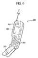
- FIG. 6is a perspective view showing an embodiment where the electronic apparatus of the present invention is applied to a cellular phone.
- FIG. 7is a perspective view showing an embodiment where the electronic apparatus of the present invention is applied to a digital still camera.
- FIG. 8is a perspective view showing an embodiment where the electronic apparatus of the present invention is applied to an electronic book.
- FIG. 9is a perspective view showing an embodiment where the electronic apparatus of the present invention is applied to an electronic paper.
- FIG. 10is a perspective view showing an embodiment where the electronic apparatus of the present invention is applied to an electronic notebook.
- FIGS. 11A and 11Bare schematic views showing an embodiment where the electronic apparatus of the present invention is applied to a display.
- FIG. 12Ais a plan view of the electrophoretic display device showing a structure of a conventional electrophoretic device.
- FIG. 12Bis a sectional view showing the structure of a pixel portion of the conventional electrophoretic device.
- FIGS. 13A to 13Eare sectional views showing a case where a conventional electrophoretic device has four pixel electrodes.
- FIGS. 14A to 14Care sectional views showing electrophoretic particles in a conventional electrophoretic device.
- FIG. 1shows a first embodiment of an electrophoretic device according to the present invention, wherein FIG. 1A is a sectional view of a pixel, and FIGS. 1B and 1C show the pixel structure.
- the present electrophoretic deviceincludes a first substrate 30 , a common electrode 8 formed on the first substrate, a second substrate 31 , a insulating layer 32 , a pixel electrode 7 arranged on the common electrode side of the second substrate, and a voltage supply circuit 13 which supplies a first voltage or a second voltage to the pixel electrode.
- the pixel electrode 7 and the common electrode 8are arranged to oppose each other with a predetermined space formed by a member (not shown) such as a spacer, a partition, or the like.
- an electrophoretic dispersion liquid 10that includes a liquid dispersion medium 11 and electrophoretic particles 12 , is filled in the space between the pixel electrode 7 and the common electrode 8 .
- the liquid dispersion medium 11is dyed black and the electrophoretic particles 12 are white and positively charged.
- the assumptionis simply for the sake of convenience, and the liquid dispersion medium and the electrophoretic particles may be in any color.
- the direction of applying the voltageneed only be reversed, and the same principal can be applied for explanation.
- liquid dispersion medium 11water, methanol, ethanol, isopropanol, butanol, octanol, methyl cellosolve, and other alcohol-based solvents, ethyl acetate, butyl acetate, and other various esters, acetone, methylethylketone, methylisobutylketone, and other ketones, pentane, hexane, octane, and other aliphatic hydrocarbons, cyclohexane, methylcyclohexane, and other alicyclic hydrocarbons, benzene, toluene, xylene, hexylbenzene, hebutylbenzene, octylbenzene, nonylbenzene, decylbenzene, undecylbenzene, dodecylbenzene, tri
- the liquid dispersion medium 11may be substantially transparent or may be opaque. Moreover, if necessary, it may be appropriately colored with a desired color. The following can be used as a colorant to color the liquid dispersion medium 11 , though it is not limited particularly to this.
- anthraquinone series, azo series, diazo series, amine series, diamine series, and other chemical compound dyes, cochineal dye, carminic acid dye, and other natural dyesazo series, polyazo series, anthraquinone series, quinacridone series, isoindolene series, isoindolenone series, phthalocyanine series, perylene series, and other organic pigments, carbon black, silica, chromic oxide, iron oxide, titanium oxide, zinc sulphide, and other inorganic pigments alone or in mixtures.
- the electrophoretic particle 12is an organic or inorganic particle, or a compound particle that electrophoretically migrates in the dispersion medium due to the potential difference.
- the followingcan be used as the electrophoretic particle 12 , though it is not limited particularly to this.
- aniline black, carbon black, or other black pigmentstitanium dioxide, zinc oxide, antimony trioxide, and other white pigments
- monoazo, dis-azo, polyazo, and other azo-based pigmentsisoindolenone, chrome yellow, yellow iron oxide, cadmium yellow, titanium yellow, antimony, and other yellow pigments
- monoazo, dis-azo, polyazo, and other azo-based pigmentsquinacrilidone red, chrome vermillion, and other red pigments
- phthalocyanine blue, indanthrene blue, anthraquinone-based dyesprussian blue, ultramarine blue, cobalt blue, and other blue pigments
- phthalocyanine green and other green pigmentsalone or in combinations of two or more types.
- the following substancemay be added to the above-mentioned pigment: electrolyte, anionic, cationic, nonionic and other various surfactants, charge controlling agents that consist of particles of metal soap, resin, rubber, oil, varnish, compounds and the like, titanium-based coupling agent, aluminum-based coupling agent, silane-based coupling agent, and other coupling agents, various polymer dispersants that consist of a single or a plurality of block polymers such as polyethylene oxide, polystyrene, acrylic, and other macromolecules, lubricants, stabilizers, and the like.
- the voltage supply circuit 13for example, semiconductor elements such as a transistor and a diode, a mechanical switch and the like may be applied. By appropriately controlling the voltage supply circuit 13 , a desired voltage, that is, the first voltage or the second voltage is supplied to the pixel electrode 7 .
- a display region 2is constituted by N pixel electrodes 7 .
- the pixel electrodesmay be arranged comparatively at random as in FIG. 1B , or they may be arranged in matrix form as in FIG. 1C .
- orderly arrangement of pixels in matrix formis more preferable since images of complex shape can be displayed more accurately.
- the value of N in the actual display deviceis determined in consideration of the pixel size, image to be displayed, desired gradation to be expressed, and the like. As N becomes greater, possible gradation to be expressed is increased, but the size of the display region 2 is increased, leading deterioration of the image quality. The smaller the pixel size becomes, the more minute the image that can be displayed.
- the reflectanceis used for the optical characteristic
- blackthat is low reflectance state
- whitethat is high reflectance state
- the examplesare simply for the sake of convenience, and essentially similar methods may be applied to other cases, for example a case where the optical characteristic is hue, chroma, or the like.
- the proportion corresponding to the desired reflectanceis obtained based on the measurement value.
- the first voltage or the second voltageis supplied from the voltage supply circuit 13 to the respective pixel electrodes 7 .
- the proportion of the black pixel number: white pixel numbermay be N ⁇ i: i. More specifically, the first voltage is applied to (N ⁇ i) pixels and the second voltage is applied to the remaining i pixels.
- the desired reflectanceis between Ri and Ri+1, the proportion that is closer to either one of them may be employed for example.
- the overall average reflectance of the two regionsmay be the middle of Ri and Ri+1.
- the proportion of the pixel number obtained by proportional distribution calculationhas been used. That is, for example when obtaining the reflectance Ri, the control has been performed assuming that the white pixel number is (((Ri ⁇ R1)/(RN ⁇ R1)) ⁇ N) and the black pixel number is (N—white pixel number).
- the pixel size in appearanceis different from the size of the pixel electrode due to the leakage of the electric field as described above, a desired reflectance can not be obtained in such a conventional method.
- the proportion of the pixel numberis obtained using the actual measurement value, the desired reflectance can be expressed more accurately.
- FIG. 2shows a second embodiment of the electrophoretic device according to the present invention.
- FIG. 2Ashows the pixel structure.
- the display region 2includes four pixel electrodes 7 having two arranged horizontally and two vertically.
- the reflectanceis used for the optical characteristic
- blackthat is low reflectance state
- whitethat is high reflectance state
- the examplesare simply for the sake of convenience as described above.
- FIG. 2Bis an example of the reflectance measurement data in the case where the proportion of the black pixel number and the white pixel number is changed in the electrophoretic display device having such a pixel structure.
- an approximating curvecan be obtained from the data as shown in the graph.
- the proportion corresponding to the desired reflectanceis calculated.
- the first voltage or the second voltageis supplied to the respective pixel electrodes.
- the proportion of the pixel number corresponding to the desired reflectancecan be obtained using the curved line of FIG. 2C .
- FIG. 2Dshows the relationship between the desired reflectance and the actually displayed reflectance when using the above-mentioned method, and it is found that excellent linearity can be obtained. In this manner, in the method of the present invention, the desired reflectance can be expressed more accurately.
- FIG. 3is a sectional view showing the structure a pixel portion in a third embodiment of the electrophoretic device according to the present invention.
- the electrophoretic particlesinclude two different types of particles 12 a and 12 b .
- Other componentsare similar to those in the above-mentioned Embodiment 1.
- the electrophoretic particles 12 aare white and positively charged and the electrophoretic particles 12 b are black and negatively charged.
- the color of the particles and the charging polarityis not specifically limited. For example, even if the charging polarity is reversed, the direction of applying the voltage need only be reversed, and the same principal can be applied for explanation.
- the positive second voltagefor example +10V
- the common electrode 8at the earth potential (i.e., 0V)
- an electric fieldis generated from the pixel electrode to the common electrode. Therefore, the positively charged electrophoretic particles 12 a migrate toward the common electrode, and the negatively charged electrophoretic particles 12 b migrate toward the pixel electrode. Consequently, the color of the electrophoretic particles 12 a , that is white, is observed from the common electrode side.
- liquid dispersion medium 11 and the electrophoretic particle 12 in the present embodimentmaterials similar to those described in Embodiment 1 may be used.
- liquid dispersion medium 11 in the present embodimentmay be substantially transparent or may be opaque. Furthermore, if necessary, it may be appropriately colored with a desired color.
- the structuremay be that the electrophoretic particle consists of three or more different types of particles.
- multicolor displaybecomes possible by adjusting the signal (voltage) applied to the pixel electrode, and controlling the mutual distribution of the three or more different types of particles.
- a mixed color of the electrophoretic particles 12 a and the electrophoretic particles 12 bin other words, an intermediate color can also be displayed by appropriately adjusting the magnitude of the signal (voltage) applied to the pixel electrode and the length of time for applying thereto during the above-mentioned image writing operation, so as to control the distribution of the particles.
- FIG. 4is a sectional view of a pixel portion in a fourth embodiment of the electrophoretic device according to the present invention.
- the electrophoretic dispersion liquid 10is encapsulated in a microcapsule 21 , and arranged between the pixel electrode 7 and the common electrode 8 .
- Other componentsare similar to those in the above-mentioned Embodiment 2.
- the structuremay be such that the electrophoretic particles 12 included in the electrophoretic dispersion liquid 10 consist of one type particle as in the Embodiment 1, or two or more different types of particles as in the Embodiment 2.
- wall-film material of the microcapsule 21examples include for example, gelatin, polyurethane resin, polyurea resin, urea resin, melamine resin, acrylic resin, polyester resin, polyamide resin, and other various resin materials. Such material alone or in combinations of two or more types may be used.
- an interfacial polymerization methodfor example, an interfacial polymerization method, in-situ polymerization method, phase separation method, interfacial precipitation method, spray-drying method, and other various micro-capsulation methods can be used.
- the size of microcapsules used for the electrophoretic device according to the present inventionis preferably uniform. Consequently, a better display function can be demonstrated by the electrophoretic device 20 .
- the size of the microcapsules 21can be made uniform by for example, percolation, screening, segregation using difference in specific gravity and the like.
- the size of the microcapsule 21(average particle diameter) is not particularly limited, however, about 10-150 ⁇ m is preferable and about 30-100 ⁇ m is more preferable.
- the microcapsule in the present embodimentis arranged between the pixel electrode and the common electrode so as to be in contact with the opposite electrodes, and formed into a flat shape along at least either one of the pixel electrode or the common electrode. Consequently, a better display function can be demonstrated by the electrophoretic device 20 .
- the structuremay be such that a binder material is provided between the pixel electrode 7 and the common electrode 8 , and around the microcapsule 21 . That is, in the present embodiment, the binder material may be a component of the electrophoretic device.
- binder materialit is not particularly limited as long as it has a good affinity and adhesiveness with the wall-film material of the microcapsule 21 and has insulation performance.
- examples thereofinclude for example, polyethylene, chlorinated polyethylene, ethylene-vinyl acetate copolymer, ethylene-ethyl acrylate copolymer, polypropylene, ABS resin (acrylonitrile-butadiene-styrene copolymer), methyl methacrylate resin, vinyl chloride resin, vinyl chloride-vinyl acetate copolymer, vinyl chloride-vinylidene chloride copolymer, vinyl chloride-acrylic ester copolymer, vinyl chloride-methacrylic acid copolymer, vinyl chloride-acrylonitrile copolymer, ethylene-vinyl alcohol-vinyl chloride copolymer, propylene-vinyl chloride copolymer, vinylidene chloride resin, vinyl acetate resin, polyvinyl alcohol, polyvinyl formal
- Examplesalso include as other binder material, methacrylic acid-styrene copolymer, polybutylene, methyl methacrylate-butadiene-styrene copolymer, and other various resin material. Such material alone or in combinations of two or more types can be used.
- the permittivity of the binder material and the permittivity of the liquid dispersion medium 6are preferably approximately the same. Therefore, a permittivity modifier, such as 1,2-butanediol, 1,4-butanediol, and other alcohols, ketones and carboxylates, is preferably added to the binder material.
- a composite film of the microcapsule and the binder materialcan be obtained in the following way.
- the microcapsules and the permittivity modifier if necessaryare mixed into the binder material, then the obtained resin composition (emulsion or organic solvent solution) is provided on the pixel electrode or a transparent electrode by, for example, a roll coater method, roll laminator method, screen printing method, spray method, ink-jet method or other application method.
- FIG. 5Ais a sectional view showing the structure a pixel portion in a fifth embodiment of the electrophoretic device according to the present invention.
- the present electrophoretic deviceincludes the first substrate 30 , the second substrate 31 provided to oppose the first substrate, the common electrode 8 and the pixel electrode 7 formed on the second substrate, and the switching element 6 that turns ON/OFF a signal supplied to the pixel electrode. Furthermore, the electrophoretic dispersion liquid 10 that includes the liquid dispersion medium 111 and the electrophoretic particles 12 is enclosed in the space between the first substrate 30 and the second substrate 31 .
- liquid dispersion medium 11 and the electrophoretic particle 12 in the present embodimentmaterials similar to the ones described in Embodiment 1 may be used.
- the electrophoretic particles 12move horizontally with respect to the substrate according to the electric field applied between the common electrode 8 and the pixel electrode 7 . Therefore, the difference in an in-plane distribution of the particles between when the particles are deposited on the common electrode and when the particles are deposited on the pixel electrode, is used to display a picture.
- the common electrode 8is shown larger than the pixel electrode 7 .
- thisis simply for the sake of convenience and the size may be appropriately determined according to the desired image property. Therefore, there is no problem if the pixel electrode 7 is larger than the common electrode 8 or they are the same size.
- the structuremay be such that the pixel electrode 7 is overlapped on the common electrode 8 .
- FIG. 6is a perspective view showing an embodiment where the electronic apparatus of the present invention is applied to a cellular phone.
- a cellular phone 300 shown in FIG. 6has a plurality of operation buttons 301 , an ear piece 302 , a mouth piece 303 and a display panel 304 .
- the display panel 304is constituted by the above-mentioned electrophoretic device 20 .
- FIG. 7is a perspective view showing an embodiment where the electronic apparatus of the present invention is applied to a digital still camera.
- the back side of the pageis called “front face of the camera”, and the front side of the page is called “back face of the camera”.
- the connection state with external devicesis also schematically shown in FIG. 7 .
- a digital still camera 400 shown in FIG. 7has a case 401 , a display panel 402 formed on the back face of the case 401 , a light receiving unit 403 formed on a viewing side (in FIG. 7 , the front face) of the case 401 , a shutter button 404 and a circuit board 405 .
- the light receiving unit 403has, for example, an optical lens, a charge coupled device (CCD) and the like.
- the display panel 402displays based on image signals from the CCD.
- the image signal of the CCD at the time of pressing the shutter button 404is transferred and stored into the circuit board 405 .
- a video signal output terminal 406and an input-output terminal 407 for data communication are provided on a side surface of the case 401 .
- a television monitor 406 Ais connected to the video signal output terminal 406
- a personal computer 407 Ais connected to the input-output terminal 407 if necessary.
- This digital still camera 400is configured so as to output the image signal stored in the memory of the circuit board 405 to the television monitor 406 A, or the personal computer 407 A, by a predetermined operation.
- the display panel 402is constituted by the above-mentioned electrophoretic device 20 .
- FIG. 8is a perspective view showing an embodiment where the electronic apparatus of the present invention is applied to an electronic book.
- An electronic book 500 shown in FIG. 8has a book shaped frame 501 , and a turnable (openable and closable) cover 502 for the frame 501 .
- a display panel 503 having the display surface exposed and an operating member 504are installed.
- the display panel 503is constituted by the above-mentioned electrophoretic device 20 .
- FIG. 9is a perspective view showing an embodiment where the electronic apparatus of the present invention is applied to an electronic paper.
- An electronic paper 600 shown in FIG. 9has a main body 601 that is constituted by a rewritable sheet having the same texture and flexibility as that of paper, and a display unit 602 .
- the display unit 602is constituted by the above-mentioned electrophoretic device 20 .
- FIG. 10is a perspective view showing an embodiment where the electronic apparatus of the present invention is applied to an electronic notebook.
- An electronic notebook 700 shown in FIG. 10has a cover 701 , and the electronic paper 600 .
- the electronic paper 600has the above described structure, that is, a similar structure to that shown in FIG. 9 . A plurality of these are bundled together so as to be interposed in the cover 701 .
- an input device which inputs display datais also provided in the cover 701 .
- the display contentscan be changed with the electronic papers 600 in the bundled condition.
- the electronic paper 600is constituted by the above-mentioned electrophoretic device 20 .
- FIGS. 11A and 11Bshow an embodiment where the electronic apparatus of the present invention is applied to a display.
- FIG. 11Ais a sectional view
- FIG. 11Bis a plan view.
- a display (electrophoretic device) 800 shown in FIG. 11has a main body 801 , and the electronic paper 600 provided so as to be detachable with respect to the main body 801 .
- the electronic paper 600has the above described structure, that is, a similar structure to that shown in FIG. 9 .
- An insertion slot 805 into which the electronic paper 600 can be insertedis formed on the side (right side in FIG. 11 ) of the main body 801 . Moreover, two pairs of carrier rollers 802 a and 802 b are provided inside of the main body 801 . When the electronic paper 600 is inserted into the main body 801 through the insertion slot 805 , the electronic paper 600 is provided into the main body 801 while being interposed between the carrier rollers 802 a and 802 b.
- a rectangular opening 803is formed on a display side (the front side of the page in FIG. 11B ) of the main body 801 , and a transparent glass plate 804 is embedded in the opening 803 .
- the electronic paper 600 that is set into the main body 801is visible from the outside of the main body 801 . That is, the display 800 constitutes a screen which displays a picture by viewing the electronic paper 600 set into the main body 801 through the transparent glass plate 804 .
- a terminal member 806is provided on a fore-end of the electronic paper 600 in the insertion direction (left side in FIG. 11 ).
- a socket 807to which the terminal member 806 is connected in a condition where the electronic paper 600 is set into the main body 801 , is provided inside the main body 801 .
- a controller 808 and an operating part 809are electrically connected to the socket 807 .
- the electronic paper 600is detachably set into the main body 801 , and it can be portably used in a condition while detached from the main body 801 .
- the electronic paper 600is constituted by the above-mentioned electrophoretic device 20 .
- the electronic apparatus of the present inventionis not limited to application to the above-mentioned items.
- Application examplesinclude a television, a view finder type or monitor direct view type video tape recorder, a car navigation device, a pager, an electronic databook, a calculator, an electronic newspaper, a word processor, a personal computer, a work station, a videophone, a point-of-sale terminal, equipment having a touch panel, and so forth.
- the electrophoretic device 20 of the present inventioncan be applied to the display parts of these various electronic apparatus.
- the desired optical characteristiccan be accurately obtained for the gradation expression, in particular in the area gradation.
Landscapes
- Engineering & Computer Science (AREA)
- Physics & Mathematics (AREA)
- Computer Hardware Design (AREA)
- General Physics & Mathematics (AREA)
- Theoretical Computer Science (AREA)
- Electrochromic Elements, Electrophoresis, Or Variable Reflection Or Absorption Elements (AREA)
- Control Of Indicators Other Than Cathode Ray Tubes (AREA)
Abstract
Description
| Black pixel number:White pixel number | Reflectance | ||
| (0) | N:0 | R1 |
| (1) | N − 1:1 | R2 |
| (2) | N − 2:2 | R3 |
| (i) | N − i:i | Ri |
| (i + 1) | N − i − 1:i + 1 | Ri + 1 |
| (N) | 0:N | RN |
Claims (10)
Applications Claiming Priority (2)
| Application Number | Priority Date | Filing Date | Title |
|---|---|---|---|
| JP2005060532AJP4690079B2 (en) | 2005-03-04 | 2005-03-04 | Electrophoresis apparatus, driving method thereof, and electronic apparatus |
| JP2005-060532 | 2005-03-04 |
Publications (2)
| Publication Number | Publication Date |
|---|---|
| US20060197738A1 US20060197738A1 (en) | 2006-09-07 |
| US7679599B2true US7679599B2 (en) | 2010-03-16 |
Family
ID=36943663
Family Applications (1)
| Application Number | Title | Priority Date | Filing Date |
|---|---|---|---|
| US11/354,835Active2029-01-16US7679599B2 (en) | 2005-03-04 | 2006-02-16 | Electrophoretic device, method of driving electrophoretic device, and electronic apparatus |
Country Status (3)
| Country | Link |
|---|---|
| US (1) | US7679599B2 (en) |
| JP (1) | JP4690079B2 (en) |
| CN (1) | CN100476560C (en) |
Cited By (165)
| Publication number | Priority date | Publication date | Assignee | Title |
|---|---|---|---|---|
| US20080024429A1 (en)* | 2006-07-25 | 2008-01-31 | E Ink Corporation | Electrophoretic displays using gaseous fluids |
| US20080218839A1 (en)* | 2003-11-05 | 2008-09-11 | E Ink Corporation | Electro-optic displays, and materials for use therein |
| US20080266646A1 (en)* | 1995-07-20 | 2008-10-30 | E Ink Corporation | Electrophoretic displays with controlled amounts of pigment |
| US20080291129A1 (en)* | 2007-05-21 | 2008-11-27 | E Ink Corporation | Methods for driving video electro-optic displays |
| US20090000729A1 (en)* | 2007-06-29 | 2009-01-01 | E Ink Corporation | Electro-optic displays, and materials and methods for production thereof |
| US20090122389A1 (en)* | 2007-11-14 | 2009-05-14 | E Ink Corporation | Electro-optic assemblies, and adhesives and binders for use therein |
| US20090161194A1 (en)* | 2007-12-20 | 2009-06-25 | Aveso, Inc. | Electrochromic display substrate |
| US20090237776A1 (en)* | 2008-03-21 | 2009-09-24 | E Ink Corporation | Electro-optic displays, and color filters for use therein |
| US20090256799A1 (en)* | 2008-04-11 | 2009-10-15 | E Ink Corporation | Methods for driving electro-optic displays |
| US20100165005A1 (en)* | 2008-12-30 | 2010-07-01 | Sprague Robert A | Highlight color display architecture using enhanced dark state |
| US20100201651A1 (en)* | 2001-03-13 | 2010-08-12 | E Ink Corporation | Apparatus for displaying drawings |
| US20100225995A1 (en)* | 2009-03-03 | 2010-09-09 | E Ink Corporation | Electro-optic displays, and color filters for use therein |
| US20100265239A1 (en)* | 2002-04-24 | 2010-10-21 | E Ink Corporation | Processes for forming backplanes for electro-optic displays |
| US20100289736A1 (en)* | 2009-02-09 | 2010-11-18 | E Ink Corporation | Electrophoretic particles, and processes for the production thereof |
| US20110032595A1 (en)* | 2002-09-03 | 2011-02-10 | E Ink Corporation | Components and methods for use in electro-optic displays |
| US20110164307A1 (en)* | 2002-06-10 | 2011-07-07 | E Ink Corporation | Electro-optic displays, and processes for the production thereof |
| US20110217639A1 (en)* | 2010-03-02 | 2011-09-08 | Sprague Robert A | Electrophoretic display fluid |
| US8040594B2 (en) | 1997-08-28 | 2011-10-18 | E Ink Corporation | Multi-color electrophoretic displays |
| US8446664B2 (en) | 2010-04-02 | 2013-05-21 | E Ink Corporation | Electrophoretic media, and materials for use therein |
| US8649084B2 (en) | 2011-09-02 | 2014-02-11 | Sipix Imaging, Inc. | Color display devices |
| US8654436B1 (en) | 2009-10-30 | 2014-02-18 | E Ink Corporation | Particles for use in electrophoretic displays |
| US8704756B2 (en) | 2010-05-26 | 2014-04-22 | Sipix Imaging, Inc. | Color display architecture and driving methods |
| US8717664B2 (en) | 2012-10-02 | 2014-05-06 | Sipix Imaging, Inc. | Color display device |
| US8786935B2 (en) | 2011-06-02 | 2014-07-22 | Sipix Imaging, Inc. | Color electrophoretic display |
| US8797636B2 (en) | 2012-07-17 | 2014-08-05 | Sipix Imaging, Inc. | Light-enhancing structure for electrophoretic display |
| WO2014134504A1 (en) | 2013-03-01 | 2014-09-04 | E Ink Corporation | Methods for driving electro-optic displays |
| US8902153B2 (en) | 2007-08-03 | 2014-12-02 | E Ink Corporation | Electro-optic displays, and processes for their production |
| US8917439B2 (en) | 2012-02-09 | 2014-12-23 | E Ink California, Llc | Shutter mode for color display devices |
| WO2015017503A1 (en) | 2013-07-30 | 2015-02-05 | E Ink Corporation | Methods for driving electro-optic displays |
| WO2015017624A1 (en) | 2013-07-31 | 2015-02-05 | E Ink Corporation | Methods for driving electro-optic displays |
| US8964282B2 (en) | 2012-10-02 | 2015-02-24 | E Ink California, Llc | Color display device |
| US8976444B2 (en) | 2011-09-02 | 2015-03-10 | E Ink California, Llc | Color display devices |
| US9013783B2 (en) | 2011-06-02 | 2015-04-21 | E Ink California, Llc | Color electrophoretic display |
| US9116412B2 (en) | 2010-05-26 | 2015-08-25 | E Ink California, Llc | Color display architecture and driving methods |
| US9170468B2 (en) | 2013-05-17 | 2015-10-27 | E Ink California, Llc | Color display device |
| US9251736B2 (en) | 2009-01-30 | 2016-02-02 | E Ink California, Llc | Multiple voltage level driving for electrophoretic displays |
| US9285649B2 (en) | 2013-04-18 | 2016-03-15 | E Ink California, Llc | Color display device |
| US9293511B2 (en) | 1998-07-08 | 2016-03-22 | E Ink Corporation | Methods for achieving improved color in microencapsulated electrophoretic devices |
| US9310661B2 (en) | 2007-03-06 | 2016-04-12 | E Ink Corporation | Materials for use in electrophoretic displays |
| US9360733B2 (en) | 2012-10-02 | 2016-06-07 | E Ink California, Llc | Color display device |
| US9459510B2 (en) | 2013-05-17 | 2016-10-04 | E Ink California, Llc | Color display device with color filters |
| WO2016191673A1 (en) | 2015-05-27 | 2016-12-01 | E Ink Corporation | Methods and circuitry for driving display devices |
| US9513527B2 (en) | 2014-01-14 | 2016-12-06 | E Ink California, Llc | Color display device |
| US9513743B2 (en) | 2012-06-01 | 2016-12-06 | E Ink Corporation | Methods for driving electro-optic displays |
| US9529240B2 (en) | 2014-01-17 | 2016-12-27 | E Ink Corporation | Controlled polymeric material conductivity for use in a two-phase electrode layer |
| US9541814B2 (en) | 2014-02-19 | 2017-01-10 | E Ink California, Llc | Color display device |
| WO2017049020A1 (en) | 2015-09-16 | 2017-03-23 | E Ink Corporation | Apparatus and methods for driving displays |
| US9612502B2 (en) | 2002-06-10 | 2017-04-04 | E Ink Corporation | Electro-optic display with edge seal |
| US9620066B2 (en) | 2010-02-02 | 2017-04-11 | E Ink Corporation | Method for driving electro-optic displays |
| WO2017062345A1 (en) | 2015-10-06 | 2017-04-13 | E Ink Corporation | Improved low-temperature electrophoretic media |
| US9646547B2 (en) | 2013-05-17 | 2017-05-09 | E Ink California, Llc | Color display device |
| US9672766B2 (en) | 2003-03-31 | 2017-06-06 | E Ink Corporation | Methods for driving electro-optic displays |
| US9697778B2 (en) | 2013-05-14 | 2017-07-04 | E Ink Corporation | Reverse driving pulses in electrophoretic displays |
| US9721495B2 (en) | 2013-02-27 | 2017-08-01 | E Ink Corporation | Methods for driving electro-optic displays |
| US9726959B2 (en) | 2005-10-18 | 2017-08-08 | E Ink Corporation | Color electro-optic displays, and processes for the production thereof |
| WO2017139323A1 (en) | 2016-02-08 | 2017-08-17 | E Ink Corporation | Methods and apparatus for operating an electro-optic display in white mode |
| US9752034B2 (en) | 2015-11-11 | 2017-09-05 | E Ink Corporation | Functionalized quinacridone pigments |
| US9759981B2 (en) | 2014-03-18 | 2017-09-12 | E Ink California, Llc | Color display device |
| EP3220383A1 (en) | 2012-02-01 | 2017-09-20 | E Ink Corporation | Methods for driving electro-optic displays |
| US9910337B2 (en) | 2006-03-22 | 2018-03-06 | E Ink Corporation | Electro-optic media produced using ink jet printing |
| US9921451B2 (en) | 2014-09-10 | 2018-03-20 | E Ink Corporation | Colored electrophoretic displays |
| US9928810B2 (en) | 2015-01-30 | 2018-03-27 | E Ink Corporation | Font control for electro-optic displays and related apparatus and methods |
| US10037735B2 (en) | 2012-11-16 | 2018-07-31 | E Ink Corporation | Active matrix display with dual driving modes |
| US10040954B2 (en) | 2015-05-28 | 2018-08-07 | E Ink California, Llc | Electrophoretic medium comprising a mixture of charge control agents |
| US10048563B2 (en) | 2003-11-05 | 2018-08-14 | E Ink Corporation | Electro-optic displays, and materials for use therein |
| US10062337B2 (en) | 2015-10-12 | 2018-08-28 | E Ink California, Llc | Electrophoretic display device |
| WO2018160912A1 (en) | 2017-03-03 | 2018-09-07 | E Ink Corporation | Electro-optic displays and driving methods |
| WO2018164942A1 (en) | 2017-03-06 | 2018-09-13 | E Ink Corporation | Method for rendering color images |
| US10115354B2 (en) | 2009-09-15 | 2018-10-30 | E Ink California, Llc | Display controller system |
| US10147366B2 (en) | 2014-11-17 | 2018-12-04 | E Ink California, Llc | Methods for driving four particle electrophoretic display |
| US10163406B2 (en) | 2015-02-04 | 2018-12-25 | E Ink Corporation | Electro-optic displays displaying in dark mode and light mode, and related apparatus and methods |
| US10162242B2 (en) | 2013-10-11 | 2018-12-25 | E Ink California, Llc | Color display device |
| US10175550B2 (en) | 2014-11-07 | 2019-01-08 | E Ink Corporation | Applications of electro-optic displays |
| US10197883B2 (en) | 2015-01-05 | 2019-02-05 | E Ink Corporation | Electro-optic displays, and methods for driving same |
| US10270939B2 (en) | 2016-05-24 | 2019-04-23 | E Ink Corporation | Method for rendering color images |
| US10276109B2 (en) | 2016-03-09 | 2019-04-30 | E Ink Corporation | Method for driving electro-optic displays |
| US10282033B2 (en) | 2012-06-01 | 2019-05-07 | E Ink Corporation | Methods for updating electro-optic displays when drawing or writing on the display |
| US10331005B2 (en) | 2002-10-16 | 2019-06-25 | E Ink Corporation | Electrophoretic displays |
| WO2019126623A1 (en) | 2017-12-22 | 2019-06-27 | E Ink Corporation | Electro-optic displays, and methods for driving same |
| US10353266B2 (en) | 2014-09-26 | 2019-07-16 | E Ink Corporation | Color sets for low resolution dithering in reflective color displays |
| WO2019144097A1 (en) | 2018-01-22 | 2019-07-25 | E Ink Corporation | Electro-optic displays, and methods for driving same |
| US10380931B2 (en) | 2013-10-07 | 2019-08-13 | E Ink California, Llc | Driving methods for color display device |
| US10380955B2 (en) | 2014-07-09 | 2019-08-13 | E Ink California, Llc | Color display device and driving methods therefor |
| US10388233B2 (en) | 2015-08-31 | 2019-08-20 | E Ink Corporation | Devices and techniques for electronically erasing a drawing device |
| US10444592B2 (en) | 2017-03-09 | 2019-10-15 | E Ink Corporation | Methods and systems for transforming RGB image data to a reduced color set for electro-optic displays |
| US10527899B2 (en) | 2016-05-31 | 2020-01-07 | E Ink Corporation | Backplanes for electro-optic displays |
| WO2020018508A1 (en) | 2018-07-17 | 2020-01-23 | E Ink California, Llc | Electro-optic displays and driving methods |
| WO2020033175A1 (en) | 2018-08-10 | 2020-02-13 | E Ink California, Llc | Switchable light-collimating layer including bistable electrophoretic fluid |
| WO2020033787A1 (en) | 2018-08-10 | 2020-02-13 | E Ink California, Llc | Driving waveforms for switchable light-collimating layer including bistable electrophoretic fluid |
| US10573257B2 (en) | 2017-05-30 | 2020-02-25 | E Ink Corporation | Electro-optic displays |
| US10573222B2 (en) | 2015-01-05 | 2020-02-25 | E Ink Corporation | Electro-optic displays, and methods for driving same |
| US10593272B2 (en) | 2016-03-09 | 2020-03-17 | E Ink Corporation | Drivers providing DC-balanced refresh sequences for color electrophoretic displays |
| WO2020060960A1 (en) | 2018-09-17 | 2020-03-26 | E Ink Corporation | Backplanes with hexagonal and triangular electrodes |
| US10657869B2 (en) | 2014-09-10 | 2020-05-19 | E Ink Corporation | Methods for driving color electrophoretic displays |
| US10726760B2 (en) | 2013-10-07 | 2020-07-28 | E Ink California, Llc | Driving methods to produce a mixed color state for an electrophoretic display |
| US10796623B2 (en) | 2015-04-27 | 2020-10-06 | E Ink Corporation | Methods and apparatuses for driving display systems |
| US10803813B2 (en) | 2015-09-16 | 2020-10-13 | E Ink Corporation | Apparatus and methods for driving displays |
| US10832622B2 (en) | 2017-04-04 | 2020-11-10 | E Ink Corporation | Methods for driving electro-optic displays |
| WO2020231733A1 (en) | 2019-05-10 | 2020-11-19 | E Ink Corporation | Colored electrophoretic displays |
| US10882042B2 (en) | 2017-10-18 | 2021-01-05 | E Ink Corporation | Digital microfluidic devices including dual substrates with thin-film transistors and capacitive sensing |
| US10891906B2 (en) | 2014-07-09 | 2021-01-12 | E Ink California, Llc | Color display device and driving methods therefor |
| US11004409B2 (en) | 2013-10-07 | 2021-05-11 | E Ink California, Llc | Driving methods for color display device |
| US11017705B2 (en) | 2012-10-02 | 2021-05-25 | E Ink California, Llc | Color display device including multiple pixels for driving three-particle electrophoretic media |
| US11030936B2 (en) | 2012-02-01 | 2021-06-08 | E Ink Corporation | Methods and apparatus for operating an electro-optic display in white mode |
| US11062663B2 (en) | 2018-11-30 | 2021-07-13 | E Ink California, Llc | Electro-optic displays and driving methods |
| US11087644B2 (en) | 2015-08-19 | 2021-08-10 | E Ink Corporation | Displays intended for use in architectural applications |
| US11250794B2 (en) | 2004-07-27 | 2022-02-15 | E Ink Corporation | Methods for driving electrophoretic displays using dielectrophoretic forces |
| US11257445B2 (en) | 2019-11-18 | 2022-02-22 | E Ink Corporation | Methods for driving electro-optic displays |
| US11266832B2 (en) | 2017-11-14 | 2022-03-08 | E Ink California, Llc | Electrophoretic active delivery system including porous conductive electrode layer |
| US11289036B2 (en) | 2019-11-14 | 2022-03-29 | E Ink Corporation | Methods for driving electro-optic displays |
| US11314098B2 (en) | 2018-08-10 | 2022-04-26 | E Ink California, Llc | Switchable light-collimating layer with reflector |
| US11404013B2 (en) | 2017-05-30 | 2022-08-02 | E Ink Corporation | Electro-optic displays with resistors for discharging remnant charges |
| US11423852B2 (en) | 2017-09-12 | 2022-08-23 | E Ink Corporation | Methods for driving electro-optic displays |
| US11422427B2 (en) | 2017-12-19 | 2022-08-23 | E Ink Corporation | Applications of electro-optic displays |
| US11450262B2 (en) | 2020-10-01 | 2022-09-20 | E Ink Corporation | Electro-optic displays, and methods for driving same |
| US11511096B2 (en) | 2018-10-15 | 2022-11-29 | E Ink Corporation | Digital microfluidic delivery device |
| US11520179B2 (en) | 2002-09-03 | 2022-12-06 | E Ink Corporation | Method of forming an electrophoretic display having a color filter array |
| US11568786B2 (en) | 2020-05-31 | 2023-01-31 | E Ink Corporation | Electro-optic displays, and methods for driving same |
| WO2023043714A1 (en) | 2021-09-14 | 2023-03-23 | E Ink Corporation | Coordinated top electrode - drive electrode voltages for switching optical state of electrophoretic displays using positive and negative voltages of different magnitudes |
| US11620959B2 (en) | 2020-11-02 | 2023-04-04 | E Ink Corporation | Enhanced push-pull (EPP) waveforms for achieving primary color sets in multi-color electrophoretic displays |
| US11657772B2 (en) | 2020-12-08 | 2023-05-23 | E Ink Corporation | Methods for driving electro-optic displays |
| US11657774B2 (en) | 2015-09-16 | 2023-05-23 | E Ink Corporation | Apparatus and methods for driving displays |
| US11686989B2 (en) | 2020-09-15 | 2023-06-27 | E Ink Corporation | Four particle electrophoretic medium providing fast, high-contrast optical state switching |
| WO2023122142A1 (en) | 2021-12-22 | 2023-06-29 | E Ink Corporation | Methods for driving electro-optic displays |
| WO2023129533A1 (en) | 2021-12-27 | 2023-07-06 | E Ink Corporation | Methods for measuring electrical properties of electro-optic displays |
| WO2023129692A1 (en) | 2021-12-30 | 2023-07-06 | E Ink California, Llc | Methods for driving electro-optic displays |
| WO2023132958A1 (en) | 2022-01-04 | 2023-07-13 | E Ink Corporation | Electrophoretic media comprising electrophoretic particles and a combination of charge control agents |
| US11721295B2 (en) | 2017-09-12 | 2023-08-08 | E Ink Corporation | Electro-optic displays, and methods for driving same |
| US11721296B2 (en) | 2020-11-02 | 2023-08-08 | E Ink Corporation | Method and apparatus for rendering color images |
| US11733580B2 (en) | 2010-05-21 | 2023-08-22 | E Ink Corporation | Method for driving two layer variable transmission display |
| US11756494B2 (en) | 2020-11-02 | 2023-09-12 | E Ink Corporation | Driving sequences to remove prior state information from color electrophoretic displays |
| US11776496B2 (en) | 2020-09-15 | 2023-10-03 | E Ink Corporation | Driving voltages for advanced color electrophoretic displays and displays with improved driving voltages |
| WO2023211867A1 (en) | 2022-04-27 | 2023-11-02 | E Ink Corporation | Color displays configured to convert rgb image data for display on advanced color electronic paper |
| US11830448B2 (en) | 2021-11-04 | 2023-11-28 | E Ink Corporation | Methods for driving electro-optic displays |
| US11846863B2 (en) | 2020-09-15 | 2023-12-19 | E Ink Corporation | Coordinated top electrode—drive electrode voltages for switching optical state of electrophoretic displays using positive and negative voltages of different magnitudes |
| US11869451B2 (en) | 2021-11-05 | 2024-01-09 | E Ink Corporation | Multi-primary display mask-based dithering with low blooming sensitivity |
| WO2024044119A1 (en) | 2022-08-25 | 2024-02-29 | E Ink Corporation | Transitional driving modes for impulse balancing when switching between global color mode and direct update mode for electrophoretic displays |
| US11922893B2 (en) | 2021-12-22 | 2024-03-05 | E Ink Corporation | High voltage driving using top plane switching with zero voltage frames between driving frames |
| US11935495B2 (en) | 2021-08-18 | 2024-03-19 | E Ink Corporation | Methods for driving electro-optic displays |
| US11938214B2 (en) | 2019-11-27 | 2024-03-26 | E Ink Corporation | Benefit agent delivery system comprising microcells having an electrically eroding sealing layer |
| WO2024091547A1 (en) | 2022-10-25 | 2024-05-02 | E Ink Corporation | Methods for driving electro-optic displays |
| US12027129B2 (en) | 2020-08-31 | 2024-07-02 | E Ink Corporation | Electro-optic displays and driving methods |
| WO2024158855A1 (en) | 2023-01-27 | 2024-08-02 | E Ink Corporation | Multi-element pixel electrode circuits for electro-optic displays and methods for driving the same |
| WO2024182264A1 (en) | 2023-02-28 | 2024-09-06 | E Ink Corporation | Drive scheme for improved color gamut in color electrophoretic displays |
| WO2024206187A1 (en) | 2023-03-24 | 2024-10-03 | E Ink Corporation | Methods for driving electro-optic displays |
| US12125449B2 (en) | 2021-02-09 | 2024-10-22 | E Ink Corporation | Continuous waveform driving in multi-color electrophoretic displays |
| WO2024253934A1 (en) | 2023-06-05 | 2024-12-12 | E Ink Corporation | Color electrophoretic medium having four pigment particle system addressable by waveforms having four voltage levels |
| US12181767B2 (en) | 2020-09-15 | 2024-12-31 | E Ink Corporation | Five-particle electrophoretic medium with improved black optical state |
| WO2025006476A1 (en) | 2023-06-27 | 2025-01-02 | E Ink Corporation | Multi-particle electrophoretic display having low-flash image updates |
| WO2025006440A1 (en) | 2023-06-27 | 2025-01-02 | E Ink Corporation | Time-shifted waveforms for multi-particle electrophoretic displays providing low-flash image updates |
| WO2025006130A1 (en) | 2023-06-27 | 2025-01-02 | E Ink Corporation | Electrophoretic device with ambient light sensor and adaptive whiteness restoring and color balancing frontlight |
| US12190730B2 (en) | 2022-02-28 | 2025-01-07 | E Ink Corporation | Parking space management system |
| WO2025034396A1 (en) | 2023-08-08 | 2025-02-13 | E Ink Corporation | Backplanes for segmented electro-optic displays and methods of manufacturing same |
| WO2025076061A1 (en) | 2023-10-05 | 2025-04-10 | E Ink Corporation | Staged gate voltage control |
| WO2025096100A1 (en) | 2023-10-31 | 2025-05-08 | E Ink Corporation | Reflective display and projected capacitive touch sensor with shared transparent electrode |
| WO2025122853A1 (en) | 2023-12-06 | 2025-06-12 | E Ink Corporation | Method of driving a color electophoretic display to form images without dithering |
| WO2025128843A1 (en) | 2023-12-15 | 2025-06-19 | E Ink Corporation | Fast response color waveforms for multiparticle electrophoretic displays |
| US12339559B1 (en) | 2021-12-09 | 2025-06-24 | E Ink Corporation | Electro-optic displays and methods for discharging remnant voltage using backlight |
| WO2025136446A1 (en) | 2023-12-22 | 2025-06-26 | E Ink Corporation | Five-particle electrophoretic medium with improved black optical state |
| WO2025147504A1 (en) | 2024-01-05 | 2025-07-10 | E Ink Corporation | An electrophoretic medium comprising particles having a pigment core and a polymeric shell |
| WO2025147410A2 (en) | 2024-01-02 | 2025-07-10 | E Ink Corporation | Electrophoretic media comprising a cationic charge control agent |
| WO2025151355A1 (en) | 2024-01-08 | 2025-07-17 | E Ink Corporation | Electrophoretic device having an adhesive layer comprising conductive filler particles and a polymeric dispersant |
| WO2025155697A1 (en) | 2024-01-20 | 2025-07-24 | E Ink Corporation | Methods for delivering low-ghosting partial updates in color electrophoretic displays |
| WO2025155412A1 (en) | 2024-01-19 | 2025-07-24 | E Ink Corporation | Flexible segmented electro-optic displays and methods of manufacture |
| WO2025160290A1 (en) | 2024-01-24 | 2025-07-31 | E Ink Corporation | Improved methods for producing full-color epaper images with low grain |
Families Citing this family (51)
| Publication number | Priority date | Publication date | Assignee | Title |
|---|---|---|---|---|
| US7999787B2 (en) | 1995-07-20 | 2011-08-16 | E Ink Corporation | Methods for driving electrophoretic displays using dielectrophoretic forces |
| US7583251B2 (en) | 1995-07-20 | 2009-09-01 | E Ink Corporation | Dielectrophoretic displays |
| US8115729B2 (en) | 1999-05-03 | 2012-02-14 | E Ink Corporation | Electrophoretic display element with filler particles |
| US7679814B2 (en) | 2001-04-02 | 2010-03-16 | E Ink Corporation | Materials for use in electrophoretic displays |
| US8390918B2 (en) | 2001-04-02 | 2013-03-05 | E Ink Corporation | Electrophoretic displays with controlled amounts of pigment |
| US7535624B2 (en) | 2001-07-09 | 2009-05-19 | E Ink Corporation | Electro-optic display and materials for use therein |
| US8125501B2 (en) | 2001-11-20 | 2012-02-28 | E Ink Corporation | Voltage modulated driver circuits for electro-optic displays |
| US8049947B2 (en) | 2002-06-10 | 2011-11-01 | E Ink Corporation | Components and methods for use in electro-optic displays |
| US7554712B2 (en) | 2005-06-23 | 2009-06-30 | E Ink Corporation | Edge seals for, and processes for assembly of, electro-optic displays |
| US7843621B2 (en) | 2002-06-10 | 2010-11-30 | E Ink Corporation | Components and testing methods for use in the production of electro-optic displays |
| US7583427B2 (en) | 2002-06-10 | 2009-09-01 | E Ink Corporation | Components and methods for use in electro-optic displays |
| US20080024482A1 (en) | 2002-06-13 | 2008-01-31 | E Ink Corporation | Methods for driving electro-optic displays |
| US7910175B2 (en) | 2003-03-25 | 2011-03-22 | E Ink Corporation | Processes for the production of electrophoretic displays |
| US8174490B2 (en) | 2003-06-30 | 2012-05-08 | E Ink Corporation | Methods for driving electrophoretic displays |
| US7672040B2 (en) | 2003-11-05 | 2010-03-02 | E Ink Corporation | Electro-optic displays, and materials for use therein |
| US7551346B2 (en) | 2003-11-05 | 2009-06-23 | E Ink Corporation | Electro-optic displays, and materials for use therein |
| US20080136774A1 (en) | 2004-07-27 | 2008-06-12 | E Ink Corporation | Methods for driving electrophoretic displays using dielectrophoretic forces |
| US7453445B2 (en) | 2004-08-13 | 2008-11-18 | E Ink Corproation | Methods for driving electro-optic displays |
| EP1938299A4 (en) | 2005-10-18 | 2010-11-24 | E Ink Corp | Components for electro-optic displays |
| TWI350793B (en) | 2006-03-08 | 2011-10-21 | E Ink Corp | Methods for production of electro-optic displays |
| US8390301B2 (en) | 2006-03-08 | 2013-03-05 | E Ink Corporation | Electro-optic displays, and materials and methods for production thereof |
| US7843624B2 (en) | 2006-03-08 | 2010-11-30 | E Ink Corporation | Electro-optic displays, and materials and methods for production thereof |
| US8610988B2 (en) | 2006-03-09 | 2013-12-17 | E Ink Corporation | Electro-optic display with edge seal |
| US7903319B2 (en) | 2006-07-11 | 2011-03-08 | E Ink Corporation | Electrophoretic medium and display with improved image stability |
| US8018640B2 (en) | 2006-07-13 | 2011-09-13 | E Ink Corporation | Particles for use in electrophoretic displays |
| US7492497B2 (en) | 2006-08-02 | 2009-02-17 | E Ink Corporation | Multi-layer light modulator |
| US7477444B2 (en) | 2006-09-22 | 2009-01-13 | E Ink Corporation & Air Products And Chemical, Inc. | Electro-optic display and materials for use therein |
| US7986450B2 (en) | 2006-09-22 | 2011-07-26 | E Ink Corporation | Electro-optic display and materials for use therein |
| US7649666B2 (en) | 2006-12-07 | 2010-01-19 | E Ink Corporation | Components and methods for use in electro-optic displays |
| US7688497B2 (en) | 2007-01-22 | 2010-03-30 | E Ink Corporation | Multi-layer sheet for use in electro-optic displays |
| KR101256709B1 (en) | 2007-01-22 | 2013-04-19 | 이 잉크 코포레이션 | Multi-layer sheet for use in electro-optic displays |
| KR101376753B1 (en)* | 2007-03-14 | 2014-03-21 | 삼성디스플레이 주식회사 | Electrophoretic display apparatus and method of driving the same |
| TW200921499A (en)* | 2007-11-08 | 2009-05-16 | Universal Scient Ind Co Ltd | Digital information indication method and system thereof |
| CN101878393B (en)* | 2007-11-29 | 2012-04-04 | 夏普株式会社 | Light source device and display device having same |
| WO2009106132A1 (en)* | 2008-02-26 | 2009-09-03 | Hewlett-Packard Development Company, L.P. | Passive electrophoretic liquid crystal display device |
| CN102177463B (en) | 2008-04-03 | 2015-04-22 | 希毕克斯影像有限公司 | color display device |
| WO2010014359A2 (en)* | 2008-08-01 | 2010-02-04 | Sipix Imaging, Inc. | Gamma adjustment with error diffusion for electrophoretic displays |
| US8503063B2 (en)* | 2008-12-30 | 2013-08-06 | Sipix Imaging, Inc. | Multicolor display architecture using enhanced dark state |
| JP5740831B2 (en)* | 2010-04-12 | 2015-07-01 | セイコーエプソン株式会社 | Electrophoretic display device driving method, electrophoretic display device, and electronic apparatus |
| US9140952B2 (en) | 2010-04-22 | 2015-09-22 | E Ink California, Llc | Electrophoretic display with enhanced contrast |
| JP5691706B2 (en) | 2011-03-22 | 2015-04-01 | セイコーエプソン株式会社 | Control device, display device and electronic device |
| JP5803352B2 (en)* | 2011-07-04 | 2015-11-04 | セイコーエプソン株式会社 | Control device, display device, electronic device, and control method |
| US20130125910A1 (en) | 2011-11-18 | 2013-05-23 | Avon Products, Inc. | Use of Electrophoretic Microcapsules in a Cosmetic Composition |
| JP2014106289A (en) | 2012-11-26 | 2014-06-09 | Sony Corp | Display device, electronic equipment and method for driving display device |
| CN105139811B (en)* | 2015-09-30 | 2017-12-22 | 深圳市国华光电科技有限公司 | A kind of electrophoretic display device (EPD) weakens the driving method of ghost |
| JP2022509371A (en)* | 2018-10-26 | 2022-01-20 | ソルクロマ・テクノロジーズ・インコーポレイテッド | Display technology and related systems and methods incorporating fluid actuators |
| CN111474800B (en)* | 2020-05-21 | 2024-01-19 | 京东方科技集团股份有限公司 | Array substrate and preparation method thereof, electronic paper display device and driving method thereof |
| KR20250102116A (en) | 2022-02-25 | 2025-07-04 | 이 잉크 코포레이션 | Electro-optic displays with edge seal components and methods of making the same |
| JP2025512537A (en) | 2022-04-27 | 2025-04-17 | イー インク コーポレイション | Electro-optic display stack with segmented electrodes and method of making same - Patents.com |
| WO2025096239A1 (en) | 2023-10-30 | 2025-05-08 | E Ink Corporation | Electro-optic display with an electro-optic material layer having a binder comprising a polymer with a quaternary ammonium group and a method for manufacturing the same |
| CN119207260A (en)* | 2024-11-28 | 2024-12-27 | 广东志慧芯屏科技有限公司 | A folding display method based on flexible electronic paper display |
Citations (7)
| Publication number | Priority date | Publication date | Assignee | Title |
|---|---|---|---|---|
| JPS5015115A (en) | 1973-06-13 | 1975-02-18 | ||
| JPS5051695A (en) | 1973-09-07 | 1975-05-08 | ||
| JPS6486116A (en) | 1987-09-29 | 1989-03-30 | Nippon Mektron Kk | Electrophoretic display device |
| JP2000035775A (en) | 1998-07-17 | 2000-02-02 | Nok Corp | Electrophoretic display |
| US20020021483A1 (en)* | 2000-06-22 | 2002-02-21 | Seiko Epson Corporation | Method and circuit for driving electrophoretic display and electronic device using same |
| WO2002073304A2 (en) | 2001-03-14 | 2002-09-19 | Koninklijke Philips Electronics N.V. | Electrophoretic display device |
| US20050104844A1 (en)* | 2003-09-30 | 2005-05-19 | Yutaka Nakai | Electrophoretic display device and method of driving electrophoretic display device |
Family Cites Families (4)
| Publication number | Priority date | Publication date | Assignee | Title |
|---|---|---|---|---|
| JP2001109219A (en)* | 1999-10-07 | 2001-04-20 | Canon Inc | Color image forming equipment |
| JP2002103683A (en)* | 2000-10-03 | 2002-04-09 | Canon Inc | Image forming apparatus, image forming method, and storage medium |
| JP2005031264A (en)* | 2003-07-09 | 2005-02-03 | Canon Inc | Display device |
| JP4380558B2 (en)* | 2005-02-21 | 2009-12-09 | セイコーエプソン株式会社 | Electro-optical device and electronic apparatus |
- 2005
- 2005-03-04JPJP2005060532Apatent/JP4690079B2/ennot_activeExpired - Lifetime
- 2006
- 2006-02-16USUS11/354,835patent/US7679599B2/enactiveActive
- 2006-03-01CNCNB2006100198766Apatent/CN100476560C/enactiveActive
Patent Citations (9)
| Publication number | Priority date | Publication date | Assignee | Title |
|---|---|---|---|---|
| JPS5015115A (en) | 1973-06-13 | 1975-02-18 | ||
| JPS5051695A (en) | 1973-09-07 | 1975-05-08 | ||
| JPS6486116A (en) | 1987-09-29 | 1989-03-30 | Nippon Mektron Kk | Electrophoretic display device |
| JP2000035775A (en) | 1998-07-17 | 2000-02-02 | Nok Corp | Electrophoretic display |
| US20020021483A1 (en)* | 2000-06-22 | 2002-02-21 | Seiko Epson Corporation | Method and circuit for driving electrophoretic display and electronic device using same |
| WO2002073304A2 (en) | 2001-03-14 | 2002-09-19 | Koninklijke Philips Electronics N.V. | Electrophoretic display device |
| CN1459046A (en) | 2001-03-14 | 2003-11-26 | 皇家菲利浦电子有限公司 | Electrophoretic display device |
| US20040036951A1 (en)* | 2001-03-14 | 2004-02-26 | Koninklijke Philips Electronics N.V. | Eletrophoretic display device |
| US20050104844A1 (en)* | 2003-09-30 | 2005-05-19 | Yutaka Nakai | Electrophoretic display device and method of driving electrophoretic display device |
Cited By (303)
| Publication number | Priority date | Publication date | Assignee | Title |
|---|---|---|---|---|
| US20080266646A1 (en)* | 1995-07-20 | 2008-10-30 | E Ink Corporation | Electrophoretic displays with controlled amounts of pigment |
| US7848006B2 (en) | 1995-07-20 | 2010-12-07 | E Ink Corporation | Electrophoretic displays with controlled amounts of pigment |
| US8441714B2 (en) | 1997-08-28 | 2013-05-14 | E Ink Corporation | Multi-color electrophoretic displays |
| US9268191B2 (en) | 1997-08-28 | 2016-02-23 | E Ink Corporation | Multi-color electrophoretic displays |
| US8040594B2 (en) | 1997-08-28 | 2011-10-18 | E Ink Corporation | Multi-color electrophoretic displays |
| US9293511B2 (en) | 1998-07-08 | 2016-03-22 | E Ink Corporation | Methods for achieving improved color in microencapsulated electrophoretic devices |
| US20100201651A1 (en)* | 2001-03-13 | 2010-08-12 | E Ink Corporation | Apparatus for displaying drawings |
| US8553012B2 (en) | 2001-03-13 | 2013-10-08 | E Ink Corporation | Apparatus for displaying drawings |
| US20100265239A1 (en)* | 2002-04-24 | 2010-10-21 | E Ink Corporation | Processes for forming backplanes for electro-optic displays |
| US8389381B2 (en) | 2002-04-24 | 2013-03-05 | E Ink Corporation | Processes for forming backplanes for electro-optic displays |
| US8363299B2 (en) | 2002-06-10 | 2013-01-29 | E Ink Corporation | Electro-optic displays, and processes for the production thereof |
| US9921422B2 (en) | 2002-06-10 | 2018-03-20 | E Ink Corporation | Electro-optic display with edge seal |
| US9612502B2 (en) | 2002-06-10 | 2017-04-04 | E Ink Corporation | Electro-optic display with edge seal |
| US20110164307A1 (en)* | 2002-06-10 | 2011-07-07 | E Ink Corporation | Electro-optic displays, and processes for the production thereof |
| US9075280B2 (en) | 2002-09-03 | 2015-07-07 | E Ink Corporation | Components and methods for use in electro-optic displays |
| US20110032595A1 (en)* | 2002-09-03 | 2011-02-10 | E Ink Corporation | Components and methods for use in electro-optic displays |
| US11520179B2 (en) | 2002-09-03 | 2022-12-06 | E Ink Corporation | Method of forming an electrophoretic display having a color filter array |
| US10331005B2 (en) | 2002-10-16 | 2019-06-25 | E Ink Corporation | Electrophoretic displays |
| US9672766B2 (en) | 2003-03-31 | 2017-06-06 | E Ink Corporation | Methods for driving electro-optic displays |
| US10324354B2 (en) | 2003-11-05 | 2019-06-18 | E Ink Corporation | Electro-optic displays, and materials for use therein |
| US20080218839A1 (en)* | 2003-11-05 | 2008-09-11 | E Ink Corporation | Electro-optic displays, and materials for use therein |
| US10048564B2 (en) | 2003-11-05 | 2018-08-14 | E Ink Corporation | Electro-optic displays, and materials for use therein |
| US8177942B2 (en) | 2003-11-05 | 2012-05-15 | E Ink Corporation | Electro-optic displays, and materials for use therein |
| US10048563B2 (en) | 2003-11-05 | 2018-08-14 | E Ink Corporation | Electro-optic displays, and materials for use therein |
| US9152004B2 (en) | 2003-11-05 | 2015-10-06 | E Ink Corporation | Electro-optic displays, and materials for use therein |
| US9829764B2 (en) | 2003-12-05 | 2017-11-28 | E Ink Corporation | Multi-color electrophoretic displays |
| US9740076B2 (en) | 2003-12-05 | 2017-08-22 | E Ink Corporation | Multi-color electrophoretic displays |
| US11250794B2 (en) | 2004-07-27 | 2022-02-15 | E Ink Corporation | Methods for driving electrophoretic displays using dielectrophoretic forces |
| US9726959B2 (en) | 2005-10-18 | 2017-08-08 | E Ink Corporation | Color electro-optic displays, and processes for the production thereof |
| US9910337B2 (en) | 2006-03-22 | 2018-03-06 | E Ink Corporation | Electro-optic media produced using ink jet printing |
| US10444591B2 (en) | 2006-03-22 | 2019-10-15 | E Ink Corporation | Electro-optic media produced using ink jet printing |
| US20080024429A1 (en)* | 2006-07-25 | 2008-01-31 | E Ink Corporation | Electrophoretic displays using gaseous fluids |
| US9841653B2 (en) | 2007-03-06 | 2017-12-12 | E Ink Corporation | Materials for use in electrophoretic displays |
| US9310661B2 (en) | 2007-03-06 | 2016-04-12 | E Ink Corporation | Materials for use in electrophoretic displays |
| US10319313B2 (en) | 2007-05-21 | 2019-06-11 | E Ink Corporation | Methods for driving video electro-optic displays |
| US20080291129A1 (en)* | 2007-05-21 | 2008-11-27 | E Ink Corporation | Methods for driving video electro-optic displays |
| US8034209B2 (en) | 2007-06-29 | 2011-10-11 | E Ink Corporation | Electro-optic displays, and materials and methods for production thereof |
| US20090000729A1 (en)* | 2007-06-29 | 2009-01-01 | E Ink Corporation | Electro-optic displays, and materials and methods for production thereof |
| US8728266B2 (en) | 2007-06-29 | 2014-05-20 | E Ink Corporation | Electro-optic displays, and materials and methods for production thereof |
| US9554495B2 (en) | 2007-06-29 | 2017-01-24 | E Ink Corporation | Electro-optic displays, and materials and methods for production thereof |
| US8902153B2 (en) | 2007-08-03 | 2014-12-02 | E Ink Corporation | Electro-optic displays, and processes for their production |
| US9964831B2 (en) | 2007-11-14 | 2018-05-08 | E Ink Corporation | Electro-optic assemblies, and adhesives and binders for use therein |
| US20090122389A1 (en)* | 2007-11-14 | 2009-05-14 | E Ink Corporation | Electro-optic assemblies, and adhesives and binders for use therein |
| US10036930B2 (en) | 2007-11-14 | 2018-07-31 | E Ink Corporation | Electro-optic assemblies, and adhesives and binders for use therein |
| US20090161194A1 (en)* | 2007-12-20 | 2009-06-25 | Aveso, Inc. | Electrochromic display substrate |
| US8294973B2 (en)* | 2007-12-20 | 2012-10-23 | Gemalto, S.A. | Electrochromic display substrate |
| US20090237776A1 (en)* | 2008-03-21 | 2009-09-24 | E Ink Corporation | Electro-optic displays, and color filters for use therein |
| US8054526B2 (en) | 2008-03-21 | 2011-11-08 | E Ink Corporation | Electro-optic displays, and color filters for use therein |
| US8314784B2 (en) | 2008-04-11 | 2012-11-20 | E Ink Corporation | Methods for driving electro-optic displays |
| US20090256799A1 (en)* | 2008-04-11 | 2009-10-15 | E Ink Corporation | Methods for driving electro-optic displays |
| US20100165005A1 (en)* | 2008-12-30 | 2010-07-01 | Sprague Robert A | Highlight color display architecture using enhanced dark state |
| US8797258B2 (en) | 2008-12-30 | 2014-08-05 | Sipix Imaging, Inc. | Highlight color display architecture using enhanced dark state |
| US9251736B2 (en) | 2009-01-30 | 2016-02-02 | E Ink California, Llc | Multiple voltage level driving for electrophoretic displays |
| US8270064B2 (en) | 2009-02-09 | 2012-09-18 | E Ink Corporation | Electrophoretic particles, and processes for the production thereof |
| US20100289736A1 (en)* | 2009-02-09 | 2010-11-18 | E Ink Corporation | Electrophoretic particles, and processes for the production thereof |
| US8441716B2 (en) | 2009-03-03 | 2013-05-14 | E Ink Corporation | Electro-optic displays, and color filters for use therein |
| US8098418B2 (en) | 2009-03-03 | 2012-01-17 | E. Ink Corporation | Electro-optic displays, and color filters for use therein |
| US20100225995A1 (en)* | 2009-03-03 | 2010-09-09 | E Ink Corporation | Electro-optic displays, and color filters for use therein |
| US10115354B2 (en) | 2009-09-15 | 2018-10-30 | E Ink California, Llc | Display controller system |
| US8654436B1 (en) | 2009-10-30 | 2014-02-18 | E Ink Corporation | Particles for use in electrophoretic displays |
| US9881565B2 (en) | 2010-02-02 | 2018-01-30 | E Ink Corporation | Method for driving electro-optic displays |
| US9620066B2 (en) | 2010-02-02 | 2017-04-11 | E Ink Corporation | Method for driving electro-optic displays |
| US20110217639A1 (en)* | 2010-03-02 | 2011-09-08 | Sprague Robert A | Electrophoretic display fluid |
| US8446664B2 (en) | 2010-04-02 | 2013-05-21 | E Ink Corporation | Electrophoretic media, and materials for use therein |
| US11733580B2 (en) | 2010-05-21 | 2023-08-22 | E Ink Corporation | Method for driving two layer variable transmission display |
| US12158684B2 (en) | 2010-05-21 | 2024-12-03 | E Ink Corporation | Method for driving two layer variable transmission display |
| US9116412B2 (en) | 2010-05-26 | 2015-08-25 | E Ink California, Llc | Color display architecture and driving methods |
| US8704756B2 (en) | 2010-05-26 | 2014-04-22 | Sipix Imaging, Inc. | Color display architecture and driving methods |
| US8786935B2 (en) | 2011-06-02 | 2014-07-22 | Sipix Imaging, Inc. | Color electrophoretic display |
| US9013783B2 (en) | 2011-06-02 | 2015-04-21 | E Ink California, Llc | Color electrophoretic display |
| US8649084B2 (en) | 2011-09-02 | 2014-02-11 | Sipix Imaging, Inc. | Color display devices |
| US8976444B2 (en) | 2011-09-02 | 2015-03-10 | E Ink California, Llc | Color display devices |
| EP3220383A1 (en) | 2012-02-01 | 2017-09-20 | E Ink Corporation | Methods for driving electro-optic displays |
| US11657773B2 (en) | 2012-02-01 | 2023-05-23 | E Ink Corporation | Methods for driving electro-optic displays |
| EP3783597A1 (en) | 2012-02-01 | 2021-02-24 | E Ink Corporation | Methods for driving electro-optic displays |
| US11462183B2 (en) | 2012-02-01 | 2022-10-04 | E Ink Corporation | Methods for driving electro-optic displays |
| US11030936B2 (en) | 2012-02-01 | 2021-06-08 | E Ink Corporation | Methods and apparatus for operating an electro-optic display in white mode |
| US11145261B2 (en) | 2012-02-01 | 2021-10-12 | E Ink Corporation | Methods for driving electro-optic displays |
| US10672350B2 (en) | 2012-02-01 | 2020-06-02 | E Ink Corporation | Methods for driving electro-optic displays |
| US8917439B2 (en) | 2012-02-09 | 2014-12-23 | E Ink California, Llc | Shutter mode for color display devices |
| US9513743B2 (en) | 2012-06-01 | 2016-12-06 | E Ink Corporation | Methods for driving electro-optic displays |
| US10282033B2 (en) | 2012-06-01 | 2019-05-07 | E Ink Corporation | Methods for updating electro-optic displays when drawing or writing on the display |
| US9996195B2 (en) | 2012-06-01 | 2018-06-12 | E Ink Corporation | Line segment update method for electro-optic displays |
| US8797636B2 (en) | 2012-07-17 | 2014-08-05 | Sipix Imaging, Inc. | Light-enhancing structure for electrophoretic display |
| US8964282B2 (en) | 2012-10-02 | 2015-02-24 | E Ink California, Llc | Color display device |
| US9360733B2 (en) | 2012-10-02 | 2016-06-07 | E Ink California, Llc | Color display device |
| US8717664B2 (en) | 2012-10-02 | 2014-05-06 | Sipix Imaging, Inc. | Color display device |
| US11017705B2 (en) | 2012-10-02 | 2021-05-25 | E Ink California, Llc | Color display device including multiple pixels for driving three-particle electrophoretic media |
| US10332435B2 (en) | 2012-10-02 | 2019-06-25 | E Ink California, Llc | Color display device |
| US10037735B2 (en) | 2012-11-16 | 2018-07-31 | E Ink Corporation | Active matrix display with dual driving modes |
| US11145235B2 (en) | 2013-02-27 | 2021-10-12 | E Ink Corporation | Methods for driving electro-optic displays |
| US9721495B2 (en) | 2013-02-27 | 2017-08-01 | E Ink Corporation | Methods for driving electro-optic displays |
| US11545065B2 (en) | 2013-02-27 | 2023-01-03 | E Ink Corporation | Methods for driving electro-optic displays |
| US11854456B2 (en) | 2013-02-27 | 2023-12-26 | E Ink Corporation | Electro-optic displays and methods for driving the same |
| US11250761B2 (en) | 2013-03-01 | 2022-02-15 | E Ink Corporation | Methods for driving electro-optic displays |
| US10380954B2 (en) | 2013-03-01 | 2019-08-13 | E Ink Corporation | Methods for driving electro-optic displays |
| US9495918B2 (en) | 2013-03-01 | 2016-11-15 | E Ink Corporation | Methods for driving electro-optic displays |
| WO2014134504A1 (en) | 2013-03-01 | 2014-09-04 | E Ink Corporation | Methods for driving electro-optic displays |
| US9285649B2 (en) | 2013-04-18 | 2016-03-15 | E Ink California, Llc | Color display device |
| US11195481B2 (en) | 2013-05-14 | 2021-12-07 | E Ink Corporation | Color electrophoretic displays using same polarity reversing address pulse |
| US10242630B2 (en) | 2013-05-14 | 2019-03-26 | E Ink Corporation | Color electrophoretic displays using same polarity reversing address pulse |
| US9697778B2 (en) | 2013-05-14 | 2017-07-04 | E Ink Corporation | Reverse driving pulses in electrophoretic displays |
| US12243498B2 (en) | 2013-05-14 | 2025-03-04 | E Ink Corporation | Colored electrophoretic displays using same polarity reversing address pulse |
| US10475399B2 (en) | 2013-05-14 | 2019-11-12 | E Ink Corporation | Color electrophoretic displays using same polarity reversing address pulse |
| US9459510B2 (en) | 2013-05-17 | 2016-10-04 | E Ink California, Llc | Color display device with color filters |
| US9646547B2 (en) | 2013-05-17 | 2017-05-09 | E Ink California, Llc | Color display device |
| US9170468B2 (en) | 2013-05-17 | 2015-10-27 | E Ink California, Llc | Color display device |
| WO2015017503A1 (en) | 2013-07-30 | 2015-02-05 | E Ink Corporation | Methods for driving electro-optic displays |
| US9620048B2 (en) | 2013-07-30 | 2017-04-11 | E Ink Corporation | Methods for driving electro-optic displays |
| EP4156164A1 (en) | 2013-07-31 | 2023-03-29 | E Ink Corporation | Methods for driving electro-optic displays |
| WO2015017624A1 (en) | 2013-07-31 | 2015-02-05 | E Ink Corporation | Methods for driving electro-optic displays |
| US12249290B2 (en) | 2013-07-31 | 2025-03-11 | E Ink Corporation | Display controller for bistable electro-optic display |
| US11195480B2 (en) | 2013-07-31 | 2021-12-07 | E Ink Corporation | Partial update driving methods for bistable electro-optic displays and display controllers using the same |
| EP4156165A2 (en) | 2013-07-31 | 2023-03-29 | E Ink Corporation | Methods for driving electro-optic displays |
| US10380931B2 (en) | 2013-10-07 | 2019-08-13 | E Ink California, Llc | Driving methods for color display device |
| US11004409B2 (en) | 2013-10-07 | 2021-05-11 | E Ink California, Llc | Driving methods for color display device |
| US11217145B2 (en) | 2013-10-07 | 2022-01-04 | E Ink California, Llc | Driving methods to produce a mixed color state for an electrophoretic display |
| US10726760B2 (en) | 2013-10-07 | 2020-07-28 | E Ink California, Llc | Driving methods to produce a mixed color state for an electrophoretic display |
| US10162242B2 (en) | 2013-10-11 | 2018-12-25 | E Ink California, Llc | Color display device |
| US9513527B2 (en) | 2014-01-14 | 2016-12-06 | E Ink California, Llc | Color display device |
| US10234742B2 (en) | 2014-01-14 | 2019-03-19 | E Ink California, Llc | Color display device |
| US10036931B2 (en) | 2014-01-14 | 2018-07-31 | E Ink California, Llc | Color display device |
| US10151955B2 (en) | 2014-01-17 | 2018-12-11 | E Ink Corporation | Controlled polymeric material conductivity for use in a two-phase electrode layer |
| US9529240B2 (en) | 2014-01-17 | 2016-12-27 | E Ink Corporation | Controlled polymeric material conductivity for use in a two-phase electrode layer |
| US10795221B2 (en) | 2014-01-17 | 2020-10-06 | E Ink Corporation | Methods for making two-phase light-transmissive electrode layer with controlled conductivity |
| US9541814B2 (en) | 2014-02-19 | 2017-01-10 | E Ink California, Llc | Color display device |
| US9759981B2 (en) | 2014-03-18 | 2017-09-12 | E Ink California, Llc | Color display device |
| US10891906B2 (en) | 2014-07-09 | 2021-01-12 | E Ink California, Llc | Color display device and driving methods therefor |
| US10380955B2 (en) | 2014-07-09 | 2019-08-13 | E Ink California, Llc | Color display device and driving methods therefor |
| US11315505B2 (en) | 2014-07-09 | 2022-04-26 | E Ink California, Llc | Color display device and driving methods therefor |
| US12019348B2 (en) | 2014-09-10 | 2024-06-25 | E Ink Corporation | Color electrophoretic display with segmented top plane electrode to create distinct switching areas |
| US10678111B2 (en) | 2014-09-10 | 2020-06-09 | E Ink Corporation | Colored electrophoretic displays |
| US10509293B2 (en) | 2014-09-10 | 2019-12-17 | E Ink Corporation | Colored electrophoretic displays |
| US10657869B2 (en) | 2014-09-10 | 2020-05-19 | E Ink Corporation | Methods for driving color electrophoretic displays |
| US12080251B2 (en) | 2014-09-10 | 2024-09-03 | E Ink Corporation | Colored electrophoretic displays |
| US9921451B2 (en) | 2014-09-10 | 2018-03-20 | E Ink Corporation | Colored electrophoretic displays |
| EP3633662A1 (en) | 2014-09-10 | 2020-04-08 | E Ink Corporation | Colored electrophoretic displays |
| US11468855B2 (en) | 2014-09-10 | 2022-10-11 | E Ink Corporation | Colored electrophoretic displays |
| US12181766B2 (en) | 2014-09-26 | 2024-12-31 | E Ink Corporation | Color sets for low resolution dithering in reflective color displays color sets for low resolution dithering in reflective color displays |
| US10353266B2 (en) | 2014-09-26 | 2019-07-16 | E Ink Corporation | Color sets for low resolution dithering in reflective color displays |
| US11402718B2 (en) | 2014-09-26 | 2022-08-02 | E Ink Corporation | Color sets for low resolution dithering in reflective color displays |
| US11846861B2 (en) | 2014-09-26 | 2023-12-19 | E Ink Corporation | Color sets for low resolution dithering in reflective color displays color sets for low resolution dithering in reflective color displays |
| US10175550B2 (en) | 2014-11-07 | 2019-01-08 | E Ink Corporation | Applications of electro-optic displays |
| US10976634B2 (en) | 2014-11-07 | 2021-04-13 | E Ink Corporation | Applications of electro-optic displays |
| US10431168B2 (en) | 2014-11-17 | 2019-10-01 | E Ink California, Llc | Methods for driving four particle electrophoretic display |
| US10891907B2 (en) | 2014-11-17 | 2021-01-12 | E Ink California, Llc | Electrophoretic display including four particles with different charges and optical characteristics |
| US10586499B2 (en) | 2014-11-17 | 2020-03-10 | E Ink California, Llc | Electrophoretic display including four particles with different charges and optical characteristics |
| US10147366B2 (en) | 2014-11-17 | 2018-12-04 | E Ink California, Llc | Methods for driving four particle electrophoretic display |
| US10573222B2 (en) | 2015-01-05 | 2020-02-25 | E Ink Corporation | Electro-optic displays, and methods for driving same |
| US10197883B2 (en) | 2015-01-05 | 2019-02-05 | E Ink Corporation | Electro-optic displays, and methods for driving same |
| US10551713B2 (en) | 2015-01-05 | 2020-02-04 | E Ink Corporation | Electro-optic displays, and methods for driving same |
| US10901285B2 (en) | 2015-01-05 | 2021-01-26 | E Ink Corporation | Methods for driving electro-optic displays |
| US9928810B2 (en) | 2015-01-30 | 2018-03-27 | E Ink Corporation | Font control for electro-optic displays and related apparatus and methods |
| US10163406B2 (en) | 2015-02-04 | 2018-12-25 | E Ink Corporation | Electro-optic displays displaying in dark mode and light mode, and related apparatus and methods |
| US10796623B2 (en) | 2015-04-27 | 2020-10-06 | E Ink Corporation | Methods and apparatuses for driving display systems |
| WO2016191673A1 (en) | 2015-05-27 | 2016-12-01 | E Ink Corporation | Methods and circuitry for driving display devices |
| US11398197B2 (en) | 2015-05-27 | 2022-07-26 | E Ink Corporation | Methods and circuitry for driving display devices |
| US10997930B2 (en) | 2015-05-27 | 2021-05-04 | E Ink Corporation | Methods and circuitry for driving display devices |
| US10233339B2 (en) | 2015-05-28 | 2019-03-19 | E Ink California, Llc | Electrophoretic medium comprising a mixture of charge control agents |
| US10040954B2 (en) | 2015-05-28 | 2018-08-07 | E Ink California, Llc | Electrophoretic medium comprising a mixture of charge control agents |
| US11087644B2 (en) | 2015-08-19 | 2021-08-10 | E Ink Corporation | Displays intended for use in architectural applications |
| US10388233B2 (en) | 2015-08-31 | 2019-08-20 | E Ink Corporation | Devices and techniques for electronically erasing a drawing device |
| US10803813B2 (en) | 2015-09-16 | 2020-10-13 | E Ink Corporation | Apparatus and methods for driving displays |
| US11657774B2 (en) | 2015-09-16 | 2023-05-23 | E Ink Corporation | Apparatus and methods for driving displays |
| WO2017049020A1 (en) | 2015-09-16 | 2017-03-23 | E Ink Corporation | Apparatus and methods for driving displays |
| US11450286B2 (en) | 2015-09-16 | 2022-09-20 | E Ink Corporation | Apparatus and methods for driving displays |
| US11098206B2 (en) | 2015-10-06 | 2021-08-24 | E Ink Corporation | Electrophoretic media including charge control agents comprising quartenary amines and unsaturated polymeric tails |
| WO2017062345A1 (en) | 2015-10-06 | 2017-04-13 | E Ink Corporation | Improved low-temperature electrophoretic media |
| US12084595B2 (en) | 2015-10-06 | 2024-09-10 | E Ink Corporation | Electrophoretic media including charge control agents comprising quartenary amines and unsaturated polymeric tails |
| US10062337B2 (en) | 2015-10-12 | 2018-08-28 | E Ink California, Llc | Electrophoretic display device |
| US10662334B2 (en) | 2015-11-11 | 2020-05-26 | E Ink Corporation | Method of making functionalized quinacridone pigments |
| US11084935B2 (en) | 2015-11-11 | 2021-08-10 | E Ink Corporation | Method of making functionalized quinacridone pigments |
| US10196523B2 (en) | 2015-11-11 | 2019-02-05 | E Ink Corporation | Functionalized quinacridone pigments |
| US9752034B2 (en) | 2015-11-11 | 2017-09-05 | E Ink Corporation | Functionalized quinacridone pigments |
| WO2017139323A1 (en) | 2016-02-08 | 2017-08-17 | E Ink Corporation | Methods and apparatus for operating an electro-optic display in white mode |
| US11404012B2 (en) | 2016-03-09 | 2022-08-02 | E Ink Corporation | Drivers providing DC-balanced refresh sequences for color electrophoretic displays |
| US10276109B2 (en) | 2016-03-09 | 2019-04-30 | E Ink Corporation | Method for driving electro-optic displays |
| US10593272B2 (en) | 2016-03-09 | 2020-03-17 | E Ink Corporation | Drivers providing DC-balanced refresh sequences for color electrophoretic displays |
| US11030965B2 (en) | 2016-03-09 | 2021-06-08 | E Ink Corporation | Drivers providing DC-balanced refresh sequences for color electrophoretic displays |
| US10554854B2 (en) | 2016-05-24 | 2020-02-04 | E Ink Corporation | Method for rendering color images |
| US11265443B2 (en) | 2016-05-24 | 2022-03-01 | E Ink Corporation | System for rendering color images |
| US10771652B2 (en) | 2016-05-24 | 2020-09-08 | E Ink Corporation | Method for rendering color images |
| US10270939B2 (en) | 2016-05-24 | 2019-04-23 | E Ink Corporation | Method for rendering color images |
| US10527899B2 (en) | 2016-05-31 | 2020-01-07 | E Ink Corporation | Backplanes for electro-optic displays |
| WO2018160912A1 (en) | 2017-03-03 | 2018-09-07 | E Ink Corporation | Electro-optic displays and driving methods |
| US10852568B2 (en) | 2017-03-03 | 2020-12-01 | E Ink Corporation | Electro-optic displays and driving methods |
| US12100369B2 (en) | 2017-03-06 | 2024-09-24 | E Ink Corporation | Method for rendering color images |
| WO2018164942A1 (en) | 2017-03-06 | 2018-09-13 | E Ink Corporation | Method for rendering color images |
| US11527216B2 (en) | 2017-03-06 | 2022-12-13 | E Ink Corporation | Method for rendering color images |
| US11094288B2 (en) | 2017-03-06 | 2021-08-17 | E Ink Corporation | Method and apparatus for rendering color images |
| US10467984B2 (en) | 2017-03-06 | 2019-11-05 | E Ink Corporation | Method for rendering color images |
| US10444592B2 (en) | 2017-03-09 | 2019-10-15 | E Ink Corporation | Methods and systems for transforming RGB image data to a reduced color set for electro-optic displays |
| US11398196B2 (en) | 2017-04-04 | 2022-07-26 | E Ink Corporation | Methods for driving electro-optic displays |
| US10832622B2 (en) | 2017-04-04 | 2020-11-10 | E Ink Corporation | Methods for driving electro-optic displays |
| US10573257B2 (en) | 2017-05-30 | 2020-02-25 | E Ink Corporation | Electro-optic displays |
| US11404013B2 (en) | 2017-05-30 | 2022-08-02 | E Ink Corporation | Electro-optic displays with resistors for discharging remnant charges |
| US10825405B2 (en) | 2017-05-30 | 2020-11-03 | E Ink Corporatior | Electro-optic displays |
| US11107425B2 (en) | 2017-05-30 | 2021-08-31 | E Ink Corporation | Electro-optic displays with resistors for discharging remnant charges |
| US11423852B2 (en) | 2017-09-12 | 2022-08-23 | E Ink Corporation | Methods for driving electro-optic displays |
| US11568827B2 (en) | 2017-09-12 | 2023-01-31 | E Ink Corporation | Methods for driving electro-optic displays to minimize edge ghosting |
| US11721295B2 (en) | 2017-09-12 | 2023-08-08 | E Ink Corporation | Electro-optic displays, and methods for driving same |
| US11935496B2 (en) | 2017-09-12 | 2024-03-19 | E Ink Corporation | Electro-optic displays, and methods for driving same |
| US10882042B2 (en) | 2017-10-18 | 2021-01-05 | E Ink Corporation | Digital microfluidic devices including dual substrates with thin-film transistors and capacitive sensing |
| US11266832B2 (en) | 2017-11-14 | 2022-03-08 | E Ink California, Llc | Electrophoretic active delivery system including porous conductive electrode layer |
| US11422427B2 (en) | 2017-12-19 | 2022-08-23 | E Ink Corporation | Applications of electro-optic displays |
| US12130530B2 (en) | 2017-12-19 | 2024-10-29 | E Ink Corporation | Applications of electro-optic displays |
| WO2019126623A1 (en) | 2017-12-22 | 2019-06-27 | E Ink Corporation | Electro-optic displays, and methods for driving same |
| WO2019144097A1 (en) | 2018-01-22 | 2019-07-25 | E Ink Corporation | Electro-optic displays, and methods for driving same |
| US12253784B2 (en) | 2018-07-17 | 2025-03-18 | E Ink Corporation | Electro-optic displays and driving methods |
| US11789330B2 (en) | 2018-07-17 | 2023-10-17 | E Ink California, Llc | Electro-optic displays and driving methods |
| WO2020018508A1 (en) | 2018-07-17 | 2020-01-23 | E Ink California, Llc | Electro-optic displays and driving methods |
| US11656526B2 (en) | 2018-08-10 | 2023-05-23 | E Ink California, Llc | Switchable light-collimating layer including bistable electrophoretic fluid |
| US11397366B2 (en) | 2018-08-10 | 2022-07-26 | E Ink California, Llc | Switchable light-collimating layer including bistable electrophoretic fluid |
| US11435606B2 (en) | 2018-08-10 | 2022-09-06 | E Ink California, Llc | Driving waveforms for switchable light-collimating layer including bistable electrophoretic fluid |
| WO2020033175A1 (en) | 2018-08-10 | 2020-02-13 | E Ink California, Llc | Switchable light-collimating layer including bistable electrophoretic fluid |
| WO2020033787A1 (en) | 2018-08-10 | 2020-02-13 | E Ink California, Llc | Driving waveforms for switchable light-collimating layer including bistable electrophoretic fluid |
| US11314098B2 (en) | 2018-08-10 | 2022-04-26 | E Ink California, Llc | Switchable light-collimating layer with reflector |
| US11719953B2 (en) | 2018-08-10 | 2023-08-08 | E Ink California, Llc | Switchable light-collimating layer with reflector |
| WO2020060960A1 (en) | 2018-09-17 | 2020-03-26 | E Ink Corporation | Backplanes with hexagonal and triangular electrodes |
| US11353759B2 (en) | 2018-09-17 | 2022-06-07 | Nuclera Nucleics Ltd. | Backplanes with hexagonal and triangular electrodes |
| US11511096B2 (en) | 2018-10-15 | 2022-11-29 | E Ink Corporation | Digital microfluidic delivery device |
| US12186514B2 (en) | 2018-10-15 | 2025-01-07 | E Ink Corporation | Digital microfluidic delivery device |
| US11380274B2 (en) | 2018-11-30 | 2022-07-05 | E Ink California, Llc | Electro-optic displays and driving methods |
| US11735127B2 (en) | 2018-11-30 | 2023-08-22 | E Ink California, Llc | Electro-optic displays and driving methods |
| US11062663B2 (en) | 2018-11-30 | 2021-07-13 | E Ink California, Llc | Electro-optic displays and driving methods |
| US11460722B2 (en) | 2019-05-10 | 2022-10-04 | E Ink Corporation | Colored electrophoretic displays |
| WO2020231733A1 (en) | 2019-05-10 | 2020-11-19 | E Ink Corporation | Colored electrophoretic displays |
| US11289036B2 (en) | 2019-11-14 | 2022-03-29 | E Ink Corporation | Methods for driving electro-optic displays |
| US11257445B2 (en) | 2019-11-18 | 2022-02-22 | E Ink Corporation | Methods for driving electro-optic displays |
| US11938215B2 (en) | 2019-11-27 | 2024-03-26 | E Ink Corporation | Method for operating a benefit agent delivery system comprising microcells having an electrically eroding sealing layer |
| US11938214B2 (en) | 2019-11-27 | 2024-03-26 | E Ink Corporation | Benefit agent delivery system comprising microcells having an electrically eroding sealing layer |
| US11568786B2 (en) | 2020-05-31 | 2023-01-31 | E Ink Corporation | Electro-optic displays, and methods for driving same |
| US12347356B2 (en) | 2020-05-31 | 2025-07-01 | E Ink Corporation | Electro-optic displays, and methods for driving same |
| US12322353B2 (en) | 2020-08-31 | 2025-06-03 | E Ink Corporation | Electro-optic displays and driving methods |
| US12027129B2 (en) | 2020-08-31 | 2024-07-02 | E Ink Corporation | Electro-optic displays and driving methods |
| US11686989B2 (en) | 2020-09-15 | 2023-06-27 | E Ink Corporation | Four particle electrophoretic medium providing fast, high-contrast optical state switching |
| US12044945B2 (en) | 2020-09-15 | 2024-07-23 | E Ink Corporation | Four particle electrophoretic medium providing fast, high-contrast optical state switching |
| US12197099B2 (en) | 2020-09-15 | 2025-01-14 | E Ink Corporation | Coordinated top electrode—drive electrode voltages for switching optical state of electrophoretic displays using positive and negative voltages of different magnitudes |
| US11776496B2 (en) | 2020-09-15 | 2023-10-03 | E Ink Corporation | Driving voltages for advanced color electrophoretic displays and displays with improved driving voltages |
| US11846863B2 (en) | 2020-09-15 | 2023-12-19 | E Ink Corporation | Coordinated top electrode—drive electrode voltages for switching optical state of electrophoretic displays using positive and negative voltages of different magnitudes |
| US12181767B2 (en) | 2020-09-15 | 2024-12-31 | E Ink Corporation | Five-particle electrophoretic medium with improved black optical state |
| US12361902B2 (en) | 2020-09-15 | 2025-07-15 | E Ink Corporation | Driving voltages for advanced color electrophoretic displays and displays with improved driving voltages |
| US11837184B2 (en) | 2020-09-15 | 2023-12-05 | E Ink Corporation | Driving voltages for advanced color electrophoretic displays and displays with improved driving voltages |
| US11948523B1 (en) | 2020-09-15 | 2024-04-02 | E Ink Corporation | Driving voltages for advanced color electrophoretic displays and displays with improved driving voltages |
| US11450262B2 (en) | 2020-10-01 | 2022-09-20 | E Ink Corporation | Electro-optic displays, and methods for driving same |
| US11721296B2 (en) | 2020-11-02 | 2023-08-08 | E Ink Corporation | Method and apparatus for rendering color images |
| US12307989B2 (en) | 2020-11-02 | 2025-05-20 | E Ink Corporation | Driving sequences to remove prior state information from color electrophoretic displays |
| US11620959B2 (en) | 2020-11-02 | 2023-04-04 | E Ink Corporation | Enhanced push-pull (EPP) waveforms for achieving primary color sets in multi-color electrophoretic displays |
| US11798506B2 (en) | 2020-11-02 | 2023-10-24 | E Ink Corporation | Enhanced push-pull (EPP) waveforms for achieving primary color sets in multi-color electrophoretic displays |
| US12347398B2 (en) | 2020-11-02 | 2025-07-01 | E Ink Corporation | Enhanced push-pull (EPP) waveforms for achieving primary color sets in multi-color electrophoretic displays |
| US12087244B2 (en) | 2020-11-02 | 2024-09-10 | E Ink Corporation | Enhanced push-pull (EPP) waveforms for achieving primary color sets in multi-color electrophoretic displays |
| US11756494B2 (en) | 2020-11-02 | 2023-09-12 | E Ink Corporation | Driving sequences to remove prior state information from color electrophoretic displays |
| US11657772B2 (en) | 2020-12-08 | 2023-05-23 | E Ink Corporation | Methods for driving electro-optic displays |
| US12125449B2 (en) | 2021-02-09 | 2024-10-22 | E Ink Corporation | Continuous waveform driving in multi-color electrophoretic displays |
| US12406632B2 (en) | 2021-02-09 | 2025-09-02 | E Ink Corporation | Continuous waveform driving in multi-color electrophoretic displays |
| US12131713B2 (en) | 2021-02-09 | 2024-10-29 | E Ink Corporation | Continuous waveform driving in multi-color electrophoretic displays |
| US11935495B2 (en) | 2021-08-18 | 2024-03-19 | E Ink Corporation | Methods for driving electro-optic displays |
| WO2023043714A1 (en) | 2021-09-14 | 2023-03-23 | E Ink Corporation | Coordinated top electrode - drive electrode voltages for switching optical state of electrophoretic displays using positive and negative voltages of different magnitudes |
| US11830448B2 (en) | 2021-11-04 | 2023-11-28 | E Ink Corporation | Methods for driving electro-optic displays |
| US11869451B2 (en) | 2021-11-05 | 2024-01-09 | E Ink Corporation | Multi-primary display mask-based dithering with low blooming sensitivity |
| US12249291B2 (en) | 2021-11-05 | 2025-03-11 | E Ink Corporation | Multi-primary display mask-based dithering with low blooming sensitivity |
| US12339559B1 (en) | 2021-12-09 | 2025-06-24 | E Ink Corporation | Electro-optic displays and methods for discharging remnant voltage using backlight |
| US11922893B2 (en) | 2021-12-22 | 2024-03-05 | E Ink Corporation | High voltage driving using top plane switching with zero voltage frames between driving frames |
| WO2023122142A1 (en) | 2021-12-22 | 2023-06-29 | E Ink Corporation | Methods for driving electro-optic displays |
| US12307988B2 (en) | 2021-12-22 | 2025-05-20 | E Ink Corporation | Methods for globally applying voltages to the display pixels of electro-optic displays |
| US12400611B2 (en) | 2021-12-22 | 2025-08-26 | E Ink Corporation | High voltage driving using top plane switching with zero voltage frames between driving frames |
| WO2023129533A1 (en) | 2021-12-27 | 2023-07-06 | E Ink Corporation | Methods for measuring electrical properties of electro-optic displays |
| US12249262B2 (en) | 2021-12-27 | 2025-03-11 | E Ink Corporation | Methods for measuring electrical properties of electro-optic displays |
| US11854448B2 (en) | 2021-12-27 | 2023-12-26 | E Ink Corporation | Methods for measuring electrical properties of electro-optic displays |
| US12085829B2 (en) | 2021-12-30 | 2024-09-10 | E Ink Corporation | Methods for driving electro-optic displays |
| US12399411B2 (en) | 2021-12-30 | 2025-08-26 | E Ink Corporation | Electro-optic displays and driving methods |
| WO2023129692A1 (en) | 2021-12-30 | 2023-07-06 | E Ink California, Llc | Methods for driving electro-optic displays |
| WO2023132958A1 (en) | 2022-01-04 | 2023-07-13 | E Ink Corporation | Electrophoretic media comprising electrophoretic particles and a combination of charge control agents |
| US12190730B2 (en) | 2022-02-28 | 2025-01-07 | E Ink Corporation | Parking space management system |
| US12334029B2 (en) | 2022-04-27 | 2025-06-17 | E Ink Corporation | Color displays configured to convert RGB image data for display on advanced color electronic paper |
| WO2023211867A1 (en) | 2022-04-27 | 2023-11-02 | E Ink Corporation | Color displays configured to convert rgb image data for display on advanced color electronic paper |
| US11984088B2 (en) | 2022-04-27 | 2024-05-14 | E Ink Corporation | Color displays configured to convert RGB image data for display on advanced color electronic paper |
| WO2024044119A1 (en) | 2022-08-25 | 2024-02-29 | E Ink Corporation | Transitional driving modes for impulse balancing when switching between global color mode and direct update mode for electrophoretic displays |
| WO2024091547A1 (en) | 2022-10-25 | 2024-05-02 | E Ink Corporation | Methods for driving electro-optic displays |
| US12190836B2 (en) | 2023-01-27 | 2025-01-07 | E Ink Corporation | Multi-element pixel electrode circuits for electro-optic displays and methods for driving the same |
| WO2024158855A1 (en) | 2023-01-27 | 2024-08-02 | E Ink Corporation | Multi-element pixel electrode circuits for electro-optic displays and methods for driving the same |
| US12272324B2 (en) | 2023-02-28 | 2025-04-08 | E Ink Corporation | Drive scheme for improved color gamut in color electrophoretic displays |
| WO2024182264A1 (en) | 2023-02-28 | 2024-09-06 | E Ink Corporation | Drive scheme for improved color gamut in color electrophoretic displays |
| WO2024206187A1 (en) | 2023-03-24 | 2024-10-03 | E Ink Corporation | Methods for driving electro-optic displays |
| WO2024253934A1 (en) | 2023-06-05 | 2024-12-12 | E Ink Corporation | Color electrophoretic medium having four pigment particle system addressable by waveforms having four voltage levels |
| WO2025006476A1 (en) | 2023-06-27 | 2025-01-02 | E Ink Corporation | Multi-particle electrophoretic display having low-flash image updates |
| WO2025006130A1 (en) | 2023-06-27 | 2025-01-02 | E Ink Corporation | Electrophoretic device with ambient light sensor and adaptive whiteness restoring and color balancing frontlight |
| WO2025006440A1 (en) | 2023-06-27 | 2025-01-02 | E Ink Corporation | Time-shifted waveforms for multi-particle electrophoretic displays providing low-flash image updates |
| US12412538B2 (en) | 2023-06-27 | 2025-09-09 | E Ink Corporation | Electrophoretic device with ambient light sensor and adaptive whiteness restoring and color balancing frontlight |
| US12406631B2 (en) | 2023-06-27 | 2025-09-02 | E Ink Corporation | Multi-particle electrophoretic display having low-flash image updates |
| US12394388B2 (en) | 2023-06-27 | 2025-08-19 | E Ink Corporation | Time-shifted waveforms for multi-particle electrophoretic displays providing low-flash image updates |
| WO2025034396A1 (en) | 2023-08-08 | 2025-02-13 | E Ink Corporation | Backplanes for segmented electro-optic displays and methods of manufacturing same |
| WO2025076061A1 (en) | 2023-10-05 | 2025-04-10 | E Ink Corporation | Staged gate voltage control |
| WO2025096100A1 (en) | 2023-10-31 | 2025-05-08 | E Ink Corporation | Reflective display and projected capacitive touch sensor with shared transparent electrode |
| WO2025122853A1 (en) | 2023-12-06 | 2025-06-12 | E Ink Corporation | Method of driving a color electophoretic display to form images without dithering |
| WO2025128843A1 (en) | 2023-12-15 | 2025-06-19 | E Ink Corporation | Fast response color waveforms for multiparticle electrophoretic displays |
| WO2025136446A1 (en) | 2023-12-22 | 2025-06-26 | E Ink Corporation | Five-particle electrophoretic medium with improved black optical state |
| WO2025147410A2 (en) | 2024-01-02 | 2025-07-10 | E Ink Corporation | Electrophoretic media comprising a cationic charge control agent |
| WO2025147504A1 (en) | 2024-01-05 | 2025-07-10 | E Ink Corporation | An electrophoretic medium comprising particles having a pigment core and a polymeric shell |
| WO2025151355A1 (en) | 2024-01-08 | 2025-07-17 | E Ink Corporation | Electrophoretic device having an adhesive layer comprising conductive filler particles and a polymeric dispersant |
| WO2025155412A1 (en) | 2024-01-19 | 2025-07-24 | E Ink Corporation | Flexible segmented electro-optic displays and methods of manufacture |
| WO2025155697A1 (en) | 2024-01-20 | 2025-07-24 | E Ink Corporation | Methods for delivering low-ghosting partial updates in color electrophoretic displays |
| WO2025160290A1 (en) | 2024-01-24 | 2025-07-31 | E Ink Corporation | Improved methods for producing full-color epaper images with low grain |
Also Published As
| Publication number | Publication date |
|---|---|
| US20060197738A1 (en) | 2006-09-07 |
| HK1093782A1 (en) | 2007-03-09 |
| JP4690079B2 (en) | 2011-06-01 |
| CN100476560C (en) | 2009-04-08 |
| CN1828398A (en) | 2006-09-06 |
| JP2006243478A (en) | 2006-09-14 |
Similar Documents
| Publication | Publication Date | Title |
|---|---|---|
| US7679599B2 (en) | Electrophoretic device, method of driving electrophoretic device, and electronic apparatus | |
| US12253784B2 (en) | Electro-optic displays and driving methods | |
| JP4211312B2 (en) | Electrophoresis device, electrophoretic device driving method, electrophoretic device driving circuit, and electronic apparatus | |
| CN115019719B (en) | Driving method of color display device | |
| JP6420841B2 (en) | Driving method of color display device | |
| JP4007119B2 (en) | Method for manufacturing electrophoresis apparatus | |
| US8674978B2 (en) | Electrophoretic display, electrophoretic display device and electronic apparatus | |
| US11380274B2 (en) | Electro-optic displays and driving methods | |
| KR102789344B1 (en) | Drive sequences for removing previous state information from color electrophoretic displays | |
| US20050110743A1 (en) | Display device, method of driving display device and electronic equipment | |
| HK1093782B (en) | Electrophoretic device, method of driving electrophoretic device, and electronic apparatus | |
| JP5397040B2 (en) | Image display device and image display device | |
| HK40045242A (en) | Electro-optic displays and driving methods | |
| HK40037134A (en) | Electro-optic displays and driving methods |
Legal Events
| Date | Code | Title | Description |
|---|---|---|---|
| AS | Assignment | Owner name:SEIKO EPSON CORPORATION,JAPAN Free format text:ASSIGNMENT OF ASSIGNORS INTEREST;ASSIGNOR:KAWAI, HIDEYUKI;REEL/FRAME:017597/0067 Effective date:20060130 Owner name:E INK CORPORATION,MASSACHUSETTS Free format text:ASSIGNMENT OF ASSIGNORS INTEREST;ASSIGNOR:KAWAI, HIDEYUKI;REEL/FRAME:017597/0067 Effective date:20060130 Owner name:E INK CORPORATION, MASSACHUSETTS Free format text:ASSIGNMENT OF ASSIGNORS INTEREST;ASSIGNOR:KAWAI, HIDEYUKI;REEL/FRAME:017597/0067 Effective date:20060130 Owner name:SEIKO EPSON CORPORATION, JAPAN Free format text:ASSIGNMENT OF ASSIGNORS INTEREST;ASSIGNOR:KAWAI, HIDEYUKI;REEL/FRAME:017597/0067 Effective date:20060130 | |
| STCF | Information on status: patent grant | Free format text:PATENTED CASE | |
| FPAY | Fee payment | Year of fee payment:4 | |
| FPAY | Fee payment | Year of fee payment:8 | |
| AS | Assignment | Owner name:E INK CORPORATION, MASSACHUSETTS Free format text:ASSIGNMENT OF ASSIGNORS INTEREST;ASSIGNOR:SEIKO EPSON CORPORATION;REEL/FRAME:047072/0325 Effective date:20180901 | |
| MAFP | Maintenance fee payment | Free format text:PAYMENT OF MAINTENANCE FEE, 12TH YEAR, LARGE ENTITY (ORIGINAL EVENT CODE: M1553); ENTITY STATUS OF PATENT OWNER: LARGE ENTITY Year of fee payment:12 |