US7675782B2 - Method, system and circuit for programming a non-volatile memory array - Google Patents
Method, system and circuit for programming a non-volatile memory arrayDownload PDFInfo
- Publication number
- US7675782B2 US7675782B2US11/581,449US58144906AUS7675782B2US 7675782 B2US7675782 B2US 7675782B2US 58144906 AUS58144906 AUS 58144906AUS 7675782 B2US7675782 B2US 7675782B2
- Authority
- US
- United States
- Prior art keywords
- cells
- nvm
- threshold voltage
- programming
- pulses
- Prior art date
- Legal status (The legal status is an assumption and is not a legal conclusion. Google has not performed a legal analysis and makes no representation as to the accuracy of the status listed.)
- Expired - Fee Related
Links
- 238000000034methodMethods0.000titleclaimsabstractdescription24
- 230000008859changeEffects0.000description9
- 238000009826distributionMethods0.000description9
- 230000000875corresponding effectEffects0.000description8
- 230000002596correlated effectEffects0.000description7
- 238000010586diagramMethods0.000description6
- 230000004044responseEffects0.000description5
- 238000003491arrayMethods0.000description4
- 230000006870functionEffects0.000description4
- 230000009977dual effectEffects0.000description3
- 230000008569processEffects0.000description3
- 230000004048modificationEffects0.000description2
- 238000012986modificationMethods0.000description2
- 150000004767nitridesChemical class0.000description2
- 230000009467reductionEffects0.000description2
- 230000014759maintenance of locationEffects0.000description1
- 230000000873masking effectEffects0.000description1
- 230000008520organizationEffects0.000description1
- 229910021420polycrystalline siliconInorganic materials0.000description1
- 239000004065semiconductorSubstances0.000description1
- 230000003068static effectEffects0.000description1
- 238000006467substitution reactionMethods0.000description1
Images


Classifications
- G—PHYSICS
- G11—INFORMATION STORAGE
- G11C—STATIC STORES
- G11C11/00—Digital stores characterised by the use of particular electric or magnetic storage elements; Storage elements therefor
- G11C11/56—Digital stores characterised by the use of particular electric or magnetic storage elements; Storage elements therefor using storage elements with more than two stable states represented by steps, e.g. of voltage, current, phase, frequency
- G11C11/5621—Digital stores characterised by the use of particular electric or magnetic storage elements; Storage elements therefor using storage elements with more than two stable states represented by steps, e.g. of voltage, current, phase, frequency using charge storage in a floating gate
- G11C11/5628—Programming or writing circuits; Data input circuits
- G—PHYSICS
- G11—INFORMATION STORAGE
- G11C—STATIC STORES
- G11C11/00—Digital stores characterised by the use of particular electric or magnetic storage elements; Storage elements therefor
- G11C11/56—Digital stores characterised by the use of particular electric or magnetic storage elements; Storage elements therefor using storage elements with more than two stable states represented by steps, e.g. of voltage, current, phase, frequency
- G11C11/5671—Digital stores characterised by the use of particular electric or magnetic storage elements; Storage elements therefor using storage elements with more than two stable states represented by steps, e.g. of voltage, current, phase, frequency using charge trapping in an insulator
- G—PHYSICS
- G11—INFORMATION STORAGE
- G11C—STATIC STORES
- G11C16/00—Erasable programmable read-only memories
- G11C16/02—Erasable programmable read-only memories electrically programmable
- G11C16/06—Auxiliary circuits, e.g. for writing into memory
- G11C16/10—Programming or data input circuits
- G—PHYSICS
- G11—INFORMATION STORAGE
- G11C—STATIC STORES
- G11C16/00—Erasable programmable read-only memories
- G11C16/02—Erasable programmable read-only memories electrically programmable
- G11C16/06—Auxiliary circuits, e.g. for writing into memory
- G11C16/34—Determination of programming status, e.g. threshold voltage, overprogramming or underprogramming, retention
- G11C16/3436—Arrangements for verifying correct programming or erasure
- G11C16/3468—Prevention of overerasure or overprogramming, e.g. by verifying whilst erasing or writing
Definitions
- the present inventiongenerally relates to the field of non-volatile memory (“NVM”) cells. More specifically, the present invention relates to a system, circuit and method for programming one or more NVM cells using a multi-phase programming sequence or algorithm.
- NVMnon-volatile memory
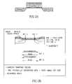
- NVM cellsare fabricated in a large variety of structures, including but not limited to Poly-silicon floating gate, as shown in FIG. 2A , and Nitride Read Only Memory (“NROM”), as shown in FIG. 2B .
- NVMNitride Read Only Memory
- an NVM cell's statemay be defined and determined by its threshold voltage, the gate to source voltage at which the cell begins to significantly conduct current.
- FIG. 1Ashows a voltage distribution graph depicting possible threshold voltage distributions of a binary non-volatile memory cell, wherein vertical lines depict boundary voltage values correlated with each of the cell's possible states. Cells having Vt Lower than EV level are said to be erased verified. Cells having Vt Higher than PV are said to be program verified. These two limits define the completion of programming and erase sequences that may be performed on a cell.
- a Program sequence of programming pulsesmay be used to drive the Vt of a cell higher than PV, while an erase sequence may drive the cell's Vt lower than EV.
- FIG. 1AAlso visible in FIG. 1A are vertical lines designating a Read Verify (RV) level and an Intermediate Program Verify voltage, PV I , designating the start of regions before the Program Verify threshold.
- RVRead Verify
- PV IIntermediate Program Verify voltage
- FIG. 1Bshows a voltage distribution graph depicting possible threshold voltage distributions in the charge storage region of a multi-level non-volatile memory cell (“MLC”), wherein one set of vertical lines depict boundary values correlated with each of the cell's possible Program Verify Threshold Voltages (PV 00 , PV 01 , etc.), another set of vertical lines depict boundary values correlated with the Read Verify level of each of the cell's possible Program states (RV 00 , RV 01 , etc.), and yet another set depict boundary lines for Intermediate Program Verify voltages (PV I 00 , PV I 01 , etc..) associated with each of the states.
- MLCmulti-level non-volatile memory cell
- the amount of charge stored in a charge storage region of an NVM cellmay be increased by applying one or more programming pulses to the cell. While the amount of charge in the cell may decrease by applying an erase pulse to the NVM cell which may force the charge reduction in the cell's charge storage region, and consequently may decrease the NVM's threshold voltage.
- a simple method used for operating NVM cellsuses one or more reference structures such as reference cells to generate the reference levels (i.e. PVs, EVs).
- Each of the one or more reference structuresmay be compared against a memory cell being operated in order to determine a condition or state of the memory cell being operated.
- the cell's threshold levelis compared to that of a reference structure whose threshold level is preset and known to be at a voltage level associated with the specific state being tested for.
- Comparing the threshold voltage of an NVM cell to that of a reference cellis often accomplished using a sense amplifier.
- Various techniques for comparing an NVM's threshold voltage against those of one or more reference cells, in order to determine the state(s) of the NVM's cellsare well known.
- a reference cell with a threshold voltage set at a voltage level defined as a “program verify” level for the given statemay be compared to the threshold voltage of the cell being programmed in order to determine whether a charge storage area or region of the cell being programmed has been sufficiently charged so as to be considered “programmed” at the desired state. If after a programming pulse has been applied to a cell, it has been determined that a cell has not been sufficiently charged in order for its threshold voltage to be at or above a “program verify” level (i.e. the threshold voltage of the relevant reference cell) associated with the target program state, the cell is typically hit with another programming pulse to try to inject more charge into its charge storage region. Once a cell's threshold value reaches or exceeds the “program verify” level to which it is being programmed, no further programming pulse should be applied to the cell.
- Groups of cells within an NVM arraymay be programmed concurrently.
- the group of NVM cellsmay consist of cells being programmed to the same logical state, or may consist of cells being programmed to several possible states, such as may be the case with MLC arrays. Since not all cells have the same susceptibility to being programmed, cells may not program at the same rate. Some cells may reach a target program state before other cells in the same set of cells that are being programmed together.
- the need to increase NVM's performancedictates more aggressive programming algorithm using stronger programming pulses.
- the stronger pulsesmay cause the Vt of the NVM cell to change significantly hence increasing the variations in the response of the different cells to the programming algorithm. This is reflected in the programming tail that may become larger using more aggressive algorithms. Larger Programming tails may not be wanted since they reduce the endurance and retention figures of an NVM cell.
- FIG. 1Billustrates four regions of an MLC, where each region is associated with one of the programmed states of the MLC. Because in an MLC a fixed range of potential threshold voltages (e.g. 3 Volts to 9 Volts) needs to be split into several sub-ranges or regions, the size of each sub-range or region in an MLC is usually smaller than a region of a binary NVM cell, as seen comparing FIG. 1A to 1B . Programming algorithms for MLC arrays may take into account that a programming tail should not exceed the read verify reference level above it.
- the present inventionis a method circuit and system for programming non-volatile memory (“NVM”) cells in an NVM array.
- NVMnon-volatile memory
- one or more NVM cells of a memory arraymay be programmed using a controller or programming circuit adapted to provide a first programming phase and a second programming phase, wherein programming pulses associated with the second programming phase may induce lower programming rate, hence lower programming variations.
- one or more NVM cells of a memory arraymay be programmed using a controller or programming circuit adapted to provide a first programming phase and a second programming phase, wherein programming pulses associated with the second programming phase may induce relatively greater threshold voltage changes in cells having less stored charge than in cells having relatively more stored charge.
- the second programming phasemay induce relatively greater threshold voltage changes in cells having relatively lower threshold voltages after the first phase programming.
- a first set of NVM cells to be programmed to a first target threshold voltage levelmay receive first phase programming pulses until one or more of the cells in the first set reaches or exceeds a first intermediate threshold voltage level, after which the cells in the first set may receive second phase programming pulses until one or more, or substantially all, of the cells in the first set reach the first target threshold voltage.
- a second set of NVM cells to be programmed to a second target threshold voltage levelmay be programmed with first phase programming pulses whose initial voltage levels may correspond to initial voltage levels associated with the second phase programming of the first set of cells.
- the second setmay receive first phase programming pulses until one or more of the cells in the second set reaches or exceeds a second intermediate threshold voltage level, after which the cells in the second set may receive second phase programming pulses until one or more, or substantially all, of the cells in the second set reach the second target threshold voltage.
- a third set of NVM cellsmay be programmed to a third target threshold voltage in a manner similar and corresponding to that describer for the first and second sets above. This process can be extended to arbitrary large number of sets of cells, associated an arbitrarily large number of target threshold voltages.
- first phase programmingmay be characterized by applying to a terminal of one or more NVM cells of a set of NVM cells incrementally increasing programming pulses in concert with pulses of substantially fixed voltage to a gate of the one or more NVM cells.
- second phase programmingmay be characterized by applying to a terminal of one or more cell of the set programming pulses of substantially fixed voltage in concert with gate pulses of incrementally increasing voltage.
- second phase programmingmay be characterized by applying to a terminal of one or more cells programming pulses of incrementally increasing voltage in concert with gate pulses of a relatively reduced and substantially fixed voltage.
- initial second phase gate and drain voltage levelsmay be deduced from a verify process of the cells during the first phase.
- FIG. 1Ashows a voltage distribution graph depicting possible threshold voltage distributions in the charge storage region of a binary non-volatile memory cell, wherein vertical lines depict boundary values or voltage threshold level correlated with the Program Verify, Read Verify and Intermediate Program Verify levels for each of the cell's possible program states;
- FIG. 1Bshows a voltage distribution graph depicting possible threshold voltage distributions in the charge storage region of a multi-level non-volatile memory cell (“MLC”), wherein sets of vertical lines depict boundary values or voltage threshold levels correlated with the Program Verify, Read Verify and Intermediate Program Verify levels for each of the cell's possible states;
- MLCmulti-level non-volatile memory cell
- FIG. 2Ashows a block diagram depicting a side cross sectional view of a floating gate memory cell
- FIG. 2Bshows a block diagram depicting a side cross sectional view of a Nitride Read Only Memory (“NROM”) cell having to distinct programming charge storage regions;
- NROMNitride Read Only Memory
- FIG. 3shows a block diagram of controller and related circuits required for programming memory cells in an array of NVM cells
- FIG. 4Ashows a time domain voltage graph illustrating a possible arrangement of programming pulses (e.g. Vds) to be applied to a terminal of an NVM cell during a first programming phase according to some embodiments of the present invention
- FIG. 4Bshows a time domain voltage graph, substantially aligned with the graph of FIG. 4A , and illustrating a possible arrangement of first phase gate pulses (Vg) corresponding to first phase programming pulses according to some embodiments of the present invention
- FIG. 4Cshows a time domain graph, substantially time aligned with the graphs of FIGS. 4A and 4B , and illustrating a change in threshold voltage of a first NVM cell receiving the pulses (e.g. Vds and Vg) of FIGS. 4A and 4B ;
- FIG. 4Dshows a time domain graph, substantially time aligned with the graphs of FIGS. 4A and 4B , and illustrating a change in threshold voltage of a second NVM cell receiving the pulses of FIGS. 4A and 4B , thus illustrating the possible variance of responses between to cells to the same set of pulses;
- FIG. 5Ashows a basic flow chart diagram depicting steps by which a set of NVM cells may be programmed to an intermediate and then a target threshold voltage as part of to a two phase programming method according to some embodiments of the present invention
- FIG. 5Bis a graph illustrating a change in threshold voltage of a first NVM cell receiving programming pulses as part of the first and second programming phases of FIG. 5A ;
- FIG. 5Cis a graph illustrating a change in threshold voltage of a second NVM cell receiving programming pulses as part of the first and second programming phases of FIG. 5A , and which cell has relatively greater changes in Vt in response to second phase programming pulses than those the cell of FIG. 5B ;
- FIG. 6Ashows two time aligned voltage graphs illustrating gate pulses (Vg) and programming pulses (Vds) to be applied to an NVM cell according to some embodiments of the present invention
- FIG. 6Bshows two time aligned voltage graphs illustrating gate pulses (Vg) and programming pulses (Vds) to be applied to an NVM cell according further embodiments of the present invention
- FIG. 7shows two sets of time aligned voltage graphs, each set illustrating the gate pulses (Vg) and programming pulses (Vds) to be applied to an NVM cell according to some embodiments of the present invention, wherein the first set of graphs illustrates pulses to be applied to an NVM cell being programmed to a first target threshold voltage (i.e. a first program state) while the second set illustrates pulses to be applied to an NVM cell being programmed to a second intermediate threshold voltage, where the initial Vds and Vg of the second cell is related to the final Vds and Vg of the of the first cell;
- Vggate pulses
- Vdsprogramming pulses
- FIG. 8shows first and second time aligned threshold voltage graphs depicting possible changes in the threshold voltages of a first and second NVM cell, where the first NVM cell was programmed with pulses depicted in the first set of graphs in FIG. 7 and the second NVM cell is programmed with pulses depicted in the second set of graphs in FIG. 7 .
- the target threshold voltage for each cellis the program verify threshold voltage to which the cell is being programmed, and the intermediate threshold voltage may be, but does not have to be, the Read Verify threshold voltage associated to the given Program Verify threshold voltage;
- FIG. 9is a flow chart illustrating steps of a first programming phase according to some embodiments of the present invention.
- FIG. 10Ais flow chart illustrating steps of a second programming phase according to some embodiments of the present invention.
- FIG. 10Bis a flow chart illustrating steps of a second programming phase according to a further embodiment of the present invention.
- the present inventionis a method circuit and system for programming non-volatile memory (“NVM”) cells in an NVM array.
- NVMnon-volatile memory
- one or more NVM cells of a memory arraymay be programmed using a controller or programming circuit adapted to provide a first programming phase and a second programming phase, wherein programming pulses associated with the second programming phase may induce relatively greater threshold voltage changes in cells having less stored charge than in cells having relatively more stored charge.
- a first set of NVM cells to be programmed to a first target threshold voltage levelmay receive first phase programming pulses until one or more of the cells in the first set reaches or exceeds a first intermediate threshold voltage level, after which the cells in the first set may receive second phase programming pulses until one or more, or substantially all, of the cells in the first set reach the first target threshold voltage.
- a second set of NVM cells to be programmed to a second target threshold voltage levelmay be programmed with first phase programming pulses whose initial voltage levels may correspond to initial voltage levels associated with the second phase programming of the first set of cells.
- the second setmay receive first phase programming pulses until one or more of the cells in the second set reaches or exceeds a second intermediate threshold voltage level, after which the cells in the second set may receive second phase programming pulses until one or more, or substantially all, of the cells in the second set reach the second target threshold voltage.
- a third set of NVM cellsmay be programmed to a third target threshold voltage in a manner similar and corresponding to that describer for the first and second sets above. This process can continue to complete a large number of sets of cells to be programmed.
- first phase programmingmay be characterized by applying to a terminal of one or more NVM cells of a set of NVM cells incrementally increasing programming pulses in concert with pulses of substantially fixed voltage to a gate of the one or more NVM cells.
- second phase programmingmay be characterized by applying to a terminal of one or more cell of the set programming pulses of substantially fixed voltage in concert with gate pulses of incrementally increasing voltage.
- second phase programmingmay be characterized by applying to a terminal of one or more cells programming pulses of incrementally increasing voltage in concert with gate pulses of a relatively reduced and substantially fixed voltage.
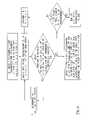
- FIG. 3there is shown a block diagram of a NVM cell array connected to controller 110 and to related circuits required for programming memory cells according to some embodiments of the present invention.
- the array 100may be comprised of either single-storage-region NVM cells or multi-storage-region (e.g. dual bit) NVM cells.
- the controller 110may be adapted to operate each charge storage region of each cell in the array 100 as either a dual level NVM cell or as a multi-level NVM cell.
- the arraymay be an array of multi-level cells in each of the above mentioned configurations.
- Data to be stored on the NVM array 100may be first received in a buffer 120 (e.g. Static Random Access Memory—SRAM) and may then be read by the controller 110 , which may respond by instructing a charge pump circuit 130 to produce first and second phase programming pulses corresponding to the data to be stored.
- the controller 110may determine to which set of NVM cells in the NVM array 100 to store the data and in what format (e.g. dual-level/binary-level, multi-level format) the data is to be stored on the selected set of cells.
- the controller 110may instruct a cell selection and masking circuit 140 to provide the charge pump circuit 130 with access to the selected cells.
- a program verify circuit 150may be used by the controller 110 to determine when a cell reaches or exceeds a given threshold voltage, for example, either the final target threshold voltage level associated with a logical state of a binary or MLC cell, or an intermediate threshold voltage associated with the above mentioned logical states.
- FIG. 4Athere is shown a time domain voltage graph illustrating a possible arrangement of programming pulses (e.g. Vds, etc.) to be applied to a terminal of an NVM cell during a first programming phase according to some embodiments of the present invention.
- FIG. 4Bshows a time domain voltage graph, substantially aligned with the graph of FIG. 4A , illustrating a possible arrangement of first phase gate pulses (Vg) corresponding to first phase programming pulses according to some embodiments of the present invention.
- Vsdsubstantially fixed gate voltage
- FIG. 4Cthere is shown a time domain graph, substantially time aligned with the graphs of FIGS. 4A and 4B , and illustrating a change in threshold voltage of a first NVM cell receiving the pulses of FIGS. 4A and 4B .
- FIG. 4Dshows a time domain graph, substantially time aligned with the graphs of FIGS. 4A and 4B , and illustrating a change in threshold voltage of a second NVM cell receiving the pulses of FIGS. 4A and 4B .
- These graphs, and more specifically the difference between them,illustrates how differently two cells may respond to the same set of programming pulses. Therefore, according to some embodiments of the present invention, first phase programming pulses may be applied to a cell or group of cells until one or more of the cells reaches an intermediate threshold level, as shown in FIGS. 4A and 4B .
- the actual threshold voltage defined as an “intermediate threshold voltage level” for a cell or set of cellsdepends on the program state to which the cell(s) is to be charged. For example, if the cell or set of cells is to be charged to first program state defined by a threshold voltage (program verify voltage) of 4.5 Volts, the target threshold voltage may be 4.5 Volts while the intermediate threshold voltage may be anywhere between 4.0 to 4.5 Volts. Likewise, if the cell or set of cells is to be charged to a second program state defined by a threshold voltage (program verify voltage) of 6 Volts, the target threshold voltage may be 6 Volts while the intermediate threshold voltage may be anywhere between 5.5 to 6 Volts.
- a threshold voltageprogram verify voltage
- first phase programming pulsesmay be followed with second phase programming pulses.
- Second phase programming pulsesmay induce greater relative threshold voltage changes in cells having less stored charge (i.e. having a lower threshold voltage) than in cells having relatively more stored charge (i.e. having higher threshold voltage).
- FIG. 5Bthere is shown a graph illustrating a change in threshold voltage of a first NVM cell receiving programming pulses as part of the first and second programming phases of the method shown in FIG. 5A
- FIG. 5Cis a graph, time/pulse aligned with FIG. 5B , illustrating a change in threshold voltage of a second NVM cell receiving programming pulses as part of the first and second programming phases of the method shown in FIG. 5A
- the first cell shown in FIG. 5Bmay charge more quickly during the first phase of programming (i.e. absorb more charge in response to each programming pulse) than the second cell shown in FIG. 5C
- the second phase programming pulsesmay be adapted to induce weaker vertical fields than those induced by first phase programming pulses, and thus the second phase programming pulses may induce greater relative charging in cells having less internally stored charge, which internally stored charge may act to cancel out portions of the induced vertical fields.
- FIG. 6Athere are shown two time aligned voltage graphs illustrating gate pulses (Vg) and programming pulses (Vds) to be applied to an NVM cell according to both phases of some embodiments of the present invention.
- Vdsprogramming pulse
- one or more cells of a set of cells to be programmed to a target threshold voltage levelmay receive programming pulse (Vds) of incrementally increasing voltage in concert with pulses of substantially fixed voltage applied to gates of the one or more NVM cells.
- Vdsprogramming pulse
- second phase programming pulses of substantially fixed voltagemay be applied in concert with gate pulses of incrementally increasing voltage.
- the substantially fixed voltage of the programming pulses during the second phasemay be at the same or related by a function to the voltage level as the last programming pulse applied during the first phase.
- FIG. 6Bthere are shown two time aligned voltage graphs illustrating gate pulses (Vg) and programming pulses (Vds) to be applied to an NVM cell according further embodiments of the present invention.
- the first phase programming pulses of FIG. 6Bare substantially identical to those of FIG. 6A .
- the second phase programming pulses depicted in FIG. 6Bshow an alternate second phase programming approach, where the programming pulses (Vds) continue to be incremented, but only the voltage level of the gate pulses are reduced.
- Vg of the second phasemay be correlated to Vg in the first phase while Vd increments can be changed between the first and second phases.
- a first set of cells to be charged/programmed to a first target threshold voltagereceive first phase programming pulses until one or more of the cells of the first set reach or exceed an first intermediate threshold voltage level correspond to the first target threshold voltage level. Once one or more cells of the first set reach to exceed the first intermediate threshold voltage level, some or all of the cells of the first set receive second phase programming pulses.
- a second set of cells to be programmed to a second target threshold voltage levelmay receive first phase programming pulse, where the voltage level of the second set's programming first phase programming pulses are a function of the last programming pulse applied to the cells of the first set during first phase programming.
- FIG. 7there is shown two sets of time aligned voltage graphs, each set illustrating the gate pulses (Vg) and programming pulses (Vds) to be applied to an NVM cell according to some embodiments of the present invention, wherein the first set of graphs illustrates pulses to be applied to an NVM cell in a first set of cells and being programmed to a first target threshold voltage (i.e. a first program state), while the second set of graphs illustrates pulses to be applied to an NVM cell in a second set of cells and being programmed to a second target threshold voltage (i.e. a second program state).
- Vggate pulses
- Vdsprogramming pulses
- the second cell in the second setmay begin first phase programming after the first cell in the first set has completed its first phase programming, and the first programming pulse applied to the second set may be of substantially the same or less or greater voltage as the last programming pulse applied to the first cell during the first programming phase.
- the cell belonging to the second setmay be programmed to a level close but not exactly to the intermediate level of the first set.
- FIG. 8there are shown first and second time aligned threshold voltage graphs depicting possible changes in the threshold voltages of a first and second NVM cell, where the first NVM cell was programmed with pulses depicted in the first set of graphs in FIG. 7 and the second NVM cell is programmed with pulses depicted in the second set of graphs in FIG. 7 .
- the concepts and methods related to FIGS. 7 and 8as they relate to the present invention are not limited to two sets of cells.
- the cell's Vtmay be checked to determine whether any of the cells have reached or exceeded the first intermediate threshold voltage. If none of the cells have reached the intermediate Vt, the Vd value may be incremented, for example by 100 mVolts, another programming pulse may be applied to the cells. This cycle may continue until one or more of the cells reaches the first intermediate Vt.
- the first set of cellsmay begin receiving second phase programming pulses, and a second set of cells may start receiving first phase programming pulses, where the initial Vd of the second set's first phase programming pulses may be related to the (e.g. substantially equal) to the find Vd applied to the first set during first phase programming.
- the second set of cellsmay continue receiving programming pulses with an incrementing Vd until one or more cells in the second reach a second intermediate Vt.
- there may be a third set, a fourth set, etc.where the voltage of the first phase programming pulses of each set of cells may be partially a function of the results of the programming of the previous set of cells.
- FIG. 10Ais flow chart illustrating steps of a second programming phase according to some embodiments of the present invention.
- the setmay receive second phase programming pulse so as to program the cells to the target threshold voltage level associated with the given intermediate level.
- FIG. 10Bthere is shown a flow chart illustrating steps of a second programming phase according to a further embodiment of the present invention.
- Vdmay be fixed at the last Vd applied to the set during first phase programming or Vd can be changed with respect to that voltage, and Vg is substantially reduced.
Landscapes
- Engineering & Computer Science (AREA)
- Computer Hardware Design (AREA)
- Read Only Memory (AREA)
- Semiconductor Memories (AREA)
Abstract
Description
Claims (12)
Priority Applications (1)
| Application Number | Priority Date | Filing Date | Title |
|---|---|---|---|
| US11/581,449US7675782B2 (en) | 2002-10-29 | 2006-10-17 | Method, system and circuit for programming a non-volatile memory array |
Applications Claiming Priority (3)
| Application Number | Priority Date | Filing Date | Title |
|---|---|---|---|
| US42178602P | 2002-10-29 | 2002-10-29 | |
| US10/695,449US7136304B2 (en) | 2002-10-29 | 2003-10-29 | Method, system and circuit for programming a non-volatile memory array |
| US11/581,449US7675782B2 (en) | 2002-10-29 | 2006-10-17 | Method, system and circuit for programming a non-volatile memory array |
Related Parent Applications (1)
| Application Number | Title | Priority Date | Filing Date |
|---|---|---|---|
| US10/695,449ContinuationUS7136304B2 (en) | 2002-10-29 | 2003-10-29 | Method, system and circuit for programming a non-volatile memory array |
Publications (2)
| Publication Number | Publication Date |
|---|---|
| US20070115726A1 US20070115726A1 (en) | 2007-05-24 |
| US7675782B2true US7675782B2 (en) | 2010-03-09 |
Family
ID=34522797
Family Applications (2)
| Application Number | Title | Priority Date | Filing Date |
|---|---|---|---|
| US10/695,449Expired - LifetimeUS7136304B2 (en) | 2002-10-29 | 2003-10-29 | Method, system and circuit for programming a non-volatile memory array |
| US11/581,449Expired - Fee RelatedUS7675782B2 (en) | 2002-10-29 | 2006-10-17 | Method, system and circuit for programming a non-volatile memory array |
Family Applications Before (1)
| Application Number | Title | Priority Date | Filing Date |
|---|---|---|---|
| US10/695,449Expired - LifetimeUS7136304B2 (en) | 2002-10-29 | 2003-10-29 | Method, system and circuit for programming a non-volatile memory array |
Country Status (6)
| Country | Link |
|---|---|
| US (2) | US7136304B2 (en) |
| EP (1) | EP1683159A4 (en) |
| JP (1) | JP2007510252A (en) |
| CN (1) | CN1902711A (en) |
| TW (1) | TWI371755B (en) |
| WO (1) | WO2005041206A2 (en) |
Cited By (4)
| Publication number | Priority date | Publication date | Assignee | Title |
|---|---|---|---|---|
| US20100128524A1 (en)* | 2008-11-24 | 2010-05-27 | Spansion Llc | Multi-phase programming of multi-level memory |
| US20100208524A1 (en)* | 2009-02-19 | 2010-08-19 | Micron Technology, Inc. | Soft landing for desired program threshold voltage |
| US8320188B2 (en) | 2010-07-28 | 2012-11-27 | SK Hynix Inc. | Semiconductor apparatus and method for transferring control voltage |
| US10664239B2 (en) | 2017-09-12 | 2020-05-26 | Ememory Technology Inc. | Method of programming nonvolatile memory cell |
Families Citing this family (104)
| Publication number | Priority date | Publication date | Assignee | Title |
|---|---|---|---|---|
| JP4170952B2 (en)* | 2004-01-30 | 2008-10-22 | 株式会社東芝 | Semiconductor memory device |
| WO2005094178A2 (en)* | 2004-04-01 | 2005-10-13 | Saifun Semiconductors Ltd. | Method, circuit and systems for erasing one or more non-volatile memory cells |
| JP4167640B2 (en)* | 2004-10-14 | 2008-10-15 | シャープ株式会社 | Method for determining program voltage of nonvolatile memory |
| US7130210B2 (en)* | 2005-01-13 | 2006-10-31 | Spansion Llc | Multi-level ONO flash program algorithm for threshold width control |
| US7339826B2 (en)* | 2005-04-11 | 2008-03-04 | Saifun Semiconductors Ltd. | Threshold voltage shift in NROM cells |
| ITVA20050024A1 (en)* | 2005-04-13 | 2006-10-14 | St Microelectronics Srl | METHOD AND CIRCUIT OF SIMULTANEOUS PROGRAMMING OF MEMORY CELLS |
| KR100719368B1 (en)* | 2005-06-27 | 2007-05-17 | 삼성전자주식회사 | Adaptive program method and device for flash memory device |
| US7656710B1 (en) | 2005-07-14 | 2010-02-02 | Sau Ching Wong | Adaptive operations for nonvolatile memories |
| KR101317625B1 (en)* | 2005-12-29 | 2013-10-10 | 샌디스크 테크놀로지스, 인코포레이티드 | Methods and device for improved program-verify operations in non-volatile memories |
| KR100683858B1 (en)* | 2006-01-12 | 2007-02-15 | 삼성전자주식회사 | Programming method of flash memory to compensate for reduction of read margin due to high temperature stress |
| KR100683856B1 (en)* | 2006-01-12 | 2007-02-15 | 삼성전자주식회사 | Programming method of flash memory to compensate for reduction of read margin due to high temperature stress |
| US7426137B2 (en)* | 2006-04-12 | 2008-09-16 | Sandisk Corporation | Apparatus for reducing the impact of program disturb during read |
| US7499326B2 (en)* | 2006-04-12 | 2009-03-03 | Sandisk Corporation | Apparatus for reducing the impact of program disturb |
| US7436713B2 (en)* | 2006-04-12 | 2008-10-14 | Sandisk Corporation | Reducing the impact of program disturb |
| US7515463B2 (en)* | 2006-04-12 | 2009-04-07 | Sandisk Corporation | Reducing the impact of program disturb during read |
| WO2007132453A2 (en)* | 2006-05-12 | 2007-11-22 | Anobit Technologies Ltd. | Distortion estimation and cancellation in memory devices |
| WO2007132456A2 (en) | 2006-05-12 | 2007-11-22 | Anobit Technologies Ltd. | Memory device with adaptive capacity |
| KR101202537B1 (en) | 2006-05-12 | 2012-11-19 | 애플 인크. | Combined distortion estimation and error correction coding for memory devices |
| WO2008026203A2 (en) | 2006-08-27 | 2008-03-06 | Anobit Technologies | Estimation of non-linear distortion in memory devices |
| US8264884B2 (en)* | 2006-09-12 | 2012-09-11 | Spansion Israel Ltd | Methods, circuits and systems for reading non-volatile memory cells |
| US7474561B2 (en) | 2006-10-10 | 2009-01-06 | Sandisk Corporation | Variable program voltage increment values in non-volatile memory program operations |
| US7450426B2 (en) | 2006-10-10 | 2008-11-11 | Sandisk Corporation | Systems utilizing variable program voltage increment values in non-volatile memory program operations |
| WO2008045805A1 (en)* | 2006-10-10 | 2008-04-17 | Sandisk Corporation | Variable program voltage increment values in non-volatile memory program operations |
| US7975192B2 (en) | 2006-10-30 | 2011-07-05 | Anobit Technologies Ltd. | Reading memory cells using multiple thresholds |
| WO2008068747A2 (en) | 2006-12-03 | 2008-06-12 | Anobit Technologies Ltd. | Automatic defect management in memory devices |
| US8151166B2 (en) | 2007-01-24 | 2012-04-03 | Anobit Technologies Ltd. | Reduction of back pattern dependency effects in memory devices |
| US7397705B1 (en)* | 2007-02-01 | 2008-07-08 | Macronix International Co., Ltd. | Method for programming multi-level cell memory array |
| US7499335B2 (en)* | 2007-02-07 | 2009-03-03 | Macronix International Co., Ltd. | Non-volatile memory with improved erasing operation |
| KR101147522B1 (en)* | 2007-02-20 | 2012-05-21 | 샌디스크 테크놀로지스, 인코포레이티드 | Dynamic verify based on threshold voltage distribution |
| US20080205140A1 (en)* | 2007-02-26 | 2008-08-28 | Aplus Flash Technology, Inc. | Bit line structure for a multilevel, dual-sided nonvolatile memory cell array |
| US8369141B2 (en) | 2007-03-12 | 2013-02-05 | Apple Inc. | Adaptive estimation of memory cell read thresholds |
| US7830713B2 (en)* | 2007-03-14 | 2010-11-09 | Aplus Flash Technology, Inc. | Bit line gate transistor structure for a multilevel, dual-sided nonvolatile memory cell NAND flash array |
| US7447068B2 (en)* | 2007-03-19 | 2008-11-04 | Macronix International Co., Ltd. | Method for programming a multilevel memory |
| ITRM20070167A1 (en)* | 2007-03-27 | 2008-09-29 | Micron Technology Inc | NON-VOLATILE MULTILEVEL MEMORY CELL PROGRAMMING |
| US8001320B2 (en) | 2007-04-22 | 2011-08-16 | Anobit Technologies Ltd. | Command interface for memory devices |
| US8234545B2 (en) | 2007-05-12 | 2012-07-31 | Apple Inc. | Data storage with incremental redundancy |
| WO2008139441A2 (en) | 2007-05-12 | 2008-11-20 | Anobit Technologies Ltd. | Memory device with internal signal processing unit |
| US8259497B2 (en) | 2007-08-06 | 2012-09-04 | Apple Inc. | Programming schemes for multi-level analog memory cells |
| US8174905B2 (en) | 2007-09-19 | 2012-05-08 | Anobit Technologies Ltd. | Programming orders for reducing distortion in arrays of multi-level analog memory cells |
| US7978520B2 (en) | 2007-09-27 | 2011-07-12 | Sandisk Corporation | Compensation of non-volatile memory chip non-idealities by program pulse adjustment |
| US8068360B2 (en) | 2007-10-19 | 2011-11-29 | Anobit Technologies Ltd. | Reading analog memory cells using built-in multi-threshold commands |
| US8000141B1 (en)* | 2007-10-19 | 2011-08-16 | Anobit Technologies Ltd. | Compensation for voltage drifts in analog memory cells |
| US8527819B2 (en) | 2007-10-19 | 2013-09-03 | Apple Inc. | Data storage in analog memory cell arrays having erase failures |
| US8270246B2 (en) | 2007-11-13 | 2012-09-18 | Apple Inc. | Optimized selection of memory chips in multi-chips memory devices |
| US8225181B2 (en) | 2007-11-30 | 2012-07-17 | Apple Inc. | Efficient re-read operations from memory devices |
| US8209588B2 (en) | 2007-12-12 | 2012-06-26 | Anobit Technologies Ltd. | Efficient interference cancellation in analog memory cell arrays |
| US8085586B2 (en) | 2007-12-27 | 2011-12-27 | Anobit Technologies Ltd. | Wear level estimation in analog memory cells |
| US8156398B2 (en) | 2008-02-05 | 2012-04-10 | Anobit Technologies Ltd. | Parameter estimation based on error correction code parity check equations |
| KR101448851B1 (en)* | 2008-02-26 | 2014-10-13 | 삼성전자주식회사 | Programming method of Non-volatile memory device |
| US8230300B2 (en) | 2008-03-07 | 2012-07-24 | Apple Inc. | Efficient readout from analog memory cells using data compression |
| US8400858B2 (en) | 2008-03-18 | 2013-03-19 | Apple Inc. | Memory device with reduced sense time readout |
| US8059457B2 (en) | 2008-03-18 | 2011-11-15 | Anobit Technologies Ltd. | Memory device with multiple-accuracy read commands |
| CN102089827B (en)* | 2008-06-12 | 2017-05-17 | 桑迪士克科技有限责任公司 | Non-volatile memory and method for associative multi-pass programming |
| US7796436B2 (en)* | 2008-07-03 | 2010-09-14 | Macronix International Co., Ltd. | Reading method for MLC memory and reading circuit using the same |
| US8498151B1 (en) | 2008-08-05 | 2013-07-30 | Apple Inc. | Data storage in analog memory cells using modified pass voltages |
| US8949684B1 (en) | 2008-09-02 | 2015-02-03 | Apple Inc. | Segmented data storage |
| US8169825B1 (en) | 2008-09-02 | 2012-05-01 | Anobit Technologies Ltd. | Reliable data storage in analog memory cells subjected to long retention periods |
| US8482978B1 (en) | 2008-09-14 | 2013-07-09 | Apple Inc. | Estimation of memory cell read thresholds by sampling inside programming level distribution intervals |
| US8000135B1 (en) | 2008-09-14 | 2011-08-16 | Anobit Technologies Ltd. | Estimation of memory cell read thresholds by sampling inside programming level distribution intervals |
| KR101468100B1 (en)* | 2008-09-23 | 2014-12-04 | 삼성전자주식회사 | Non-volatile memory device and its page buffer |
| US8239734B1 (en) | 2008-10-15 | 2012-08-07 | Apple Inc. | Efficient data storage in storage device arrays |
| US8045375B2 (en)* | 2008-10-24 | 2011-10-25 | Sandisk Technologies Inc. | Programming non-volatile memory with high resolution variable initial programming pulse |
| US8713330B1 (en) | 2008-10-30 | 2014-04-29 | Apple Inc. | Data scrambling in memory devices |
| US8208304B2 (en) | 2008-11-16 | 2012-06-26 | Anobit Technologies Ltd. | Storage at M bits/cell density in N bits/cell analog memory cell devices, M>N |
| US8248831B2 (en) | 2008-12-31 | 2012-08-21 | Apple Inc. | Rejuvenation of analog memory cells |
| US8174857B1 (en) | 2008-12-31 | 2012-05-08 | Anobit Technologies Ltd. | Efficient readout schemes for analog memory cell devices using multiple read threshold sets |
| US8924661B1 (en) | 2009-01-18 | 2014-12-30 | Apple Inc. | Memory system including a controller and processors associated with memory devices |
| KR101005117B1 (en)* | 2009-01-23 | 2011-01-04 | 주식회사 하이닉스반도체 | How Nonvolatile Memory Devices Work |
| US8228701B2 (en) | 2009-03-01 | 2012-07-24 | Apple Inc. | Selective activation of programming schemes in analog memory cell arrays |
| US8832354B2 (en) | 2009-03-25 | 2014-09-09 | Apple Inc. | Use of host system resources by memory controller |
| US8259506B1 (en) | 2009-03-25 | 2012-09-04 | Apple Inc. | Database of memory read thresholds |
| US8238157B1 (en) | 2009-04-12 | 2012-08-07 | Apple Inc. | Selective re-programming of analog memory cells |
| US8054691B2 (en)* | 2009-06-26 | 2011-11-08 | Sandisk Technologies Inc. | Detecting the completion of programming for non-volatile storage |
| US8479080B1 (en) | 2009-07-12 | 2013-07-02 | Apple Inc. | Adaptive over-provisioning in memory systems |
| US8495465B1 (en) | 2009-10-15 | 2013-07-23 | Apple Inc. | Error correction coding over multiple memory pages |
| US8223556B2 (en)* | 2009-11-25 | 2012-07-17 | Sandisk Technologies Inc. | Programming non-volatile memory with a reduced number of verify operations |
| US8677054B1 (en) | 2009-12-16 | 2014-03-18 | Apple Inc. | Memory management schemes for non-volatile memory devices |
| US8694814B1 (en) | 2010-01-10 | 2014-04-08 | Apple Inc. | Reuse of host hibernation storage space by memory controller |
| US8572311B1 (en) | 2010-01-11 | 2013-10-29 | Apple Inc. | Redundant data storage in multi-die memory systems |
| US8694853B1 (en) | 2010-05-04 | 2014-04-08 | Apple Inc. | Read commands for reading interfering memory cells |
| US8572423B1 (en) | 2010-06-22 | 2013-10-29 | Apple Inc. | Reducing peak current in memory systems |
| US8595591B1 (en) | 2010-07-11 | 2013-11-26 | Apple Inc. | Interference-aware assignment of programming levels in analog memory cells |
| US8471328B2 (en) | 2010-07-26 | 2013-06-25 | United Microelectronics Corp. | Non-volatile memory and manufacturing method thereof |
| US9104580B1 (en) | 2010-07-27 | 2015-08-11 | Apple Inc. | Cache memory for hybrid disk drives |
| US8645794B1 (en) | 2010-07-31 | 2014-02-04 | Apple Inc. | Data storage in analog memory cells using a non-integer number of bits per cell |
| US8856475B1 (en) | 2010-08-01 | 2014-10-07 | Apple Inc. | Efficient selection of memory blocks for compaction |
| US8694854B1 (en) | 2010-08-17 | 2014-04-08 | Apple Inc. | Read threshold setting based on soft readout statistics |
| US9021181B1 (en) | 2010-09-27 | 2015-04-28 | Apple Inc. | Memory management for unifying memory cell conditions by using maximum time intervals |
| CN103310839B (en)* | 2012-03-15 | 2016-01-20 | 旺宏电子股份有限公司 | Method and device for shortening erasing operation |
| US8797802B2 (en)* | 2012-03-15 | 2014-08-05 | Macronix International Co., Ltd. | Method and apparatus for shortened erase operation |
| US8837214B2 (en) | 2012-12-10 | 2014-09-16 | Apple Inc. | Applications for inter-word-line programming |
| US8824214B2 (en) | 2012-12-10 | 2014-09-02 | Apple Inc. | Inter-word-line programming in arrays of analog memory cells |
| US20140198576A1 (en)* | 2013-01-16 | 2014-07-17 | Macronix International Co, Ltd. | Programming technique for reducing program disturb in stacked memory structures |
| US8908445B2 (en) | 2013-03-15 | 2014-12-09 | Freescale Semiconductor, Inc. | Non-volatile memory (NVM) with block-size-aware program/erase |
| JP5669903B2 (en)* | 2013-09-05 | 2015-02-18 | ラピスセミコンダクタ株式会社 | Semiconductor nonvolatile memory, semiconductor nonvolatile memory charge storage method, and charge storage program |
| CN105989879B (en)* | 2015-02-06 | 2019-10-11 | 华邦电子股份有限公司 | High-reliability nonvolatile semiconductor memory device and data erasing method thereof |
| KR102452994B1 (en) | 2016-09-06 | 2022-10-12 | 에스케이하이닉스 주식회사 | Semiconductor memory device and method for operating the same |
| US10381094B2 (en) | 2016-10-11 | 2019-08-13 | Macronix International Co., Ltd. | 3D memory with staged-level multibit programming |
| US10146460B1 (en) | 2017-06-01 | 2018-12-04 | Apple Inc. | Programming schemes for avoidance or recovery from cross-temperature read failures |
| US11244734B2 (en)* | 2019-12-27 | 2022-02-08 | Sandisk Technologies Llc | Modified verify scheme for programming a memory apparatus |
| US11837299B2 (en) | 2021-04-13 | 2023-12-05 | Jmem Technology Co., Ltd | Operation method of multi-bits read only memory |
| TWI747784B (en)* | 2021-04-28 | 2021-11-21 | 國立陽明交通大學 | Operation method of a multi-bits read only memory |
| US11556416B2 (en) | 2021-05-05 | 2023-01-17 | Apple Inc. | Controlling memory readout reliability and throughput by adjusting distance between read thresholds |
| US11847342B2 (en) | 2021-07-28 | 2023-12-19 | Apple Inc. | Efficient transfer of hard data and confidence levels in reading a nonvolatile memory |
Citations (565)
| Publication number | Priority date | Publication date | Assignee | Title |
|---|---|---|---|---|
| GB1297899A (en) | 1970-10-02 | 1972-11-29 | ||
| US3881180A (en) | 1971-11-30 | 1975-04-29 | Texas Instruments Inc | Non-volatile memory cell |
| US3895360A (en) | 1974-01-29 | 1975-07-15 | Westinghouse Electric Corp | Block oriented random access memory |
| US3952325A (en) | 1971-07-28 | 1976-04-20 | U.S. Philips Corporation | Semiconductor memory elements |
| US4016588A (en) | 1974-12-27 | 1977-04-05 | Nippon Electric Company, Ltd. | Non-volatile semiconductor memory device |
| US4017888A (en) | 1975-12-31 | 1977-04-12 | International Business Machines Corporation | Non-volatile metal nitride oxide semiconductor device |
| US4145703A (en) | 1977-04-15 | 1979-03-20 | Supertex, Inc. | High power MOS device and fabrication method therefor |
| US4151021A (en) | 1977-01-26 | 1979-04-24 | Texas Instruments Incorporated | Method of making a high density floating gate electrically programmable ROM |
| US4173791A (en) | 1977-09-16 | 1979-11-06 | Fairchild Camera And Instrument Corporation | Insulated gate field-effect transistor read-only memory array |
| US4173766A (en) | 1977-09-16 | 1979-11-06 | Fairchild Camera And Instrument Corporation | Insulated gate field-effect transistor read-only memory cell |
| US4247861A (en) | 1979-03-09 | 1981-01-27 | Rca Corporation | High performance electrically alterable read-only memory (EAROM) |
| US4257832A (en) | 1978-07-24 | 1981-03-24 | Siemens Aktiengesellschaft | Process for producing an integrated multi-layer insulator memory cell |
| US4281397A (en) | 1979-10-29 | 1981-07-28 | Texas Instruments Incorporated | Virtual ground MOS EPROM or ROM matrix |
| US4306353A (en) | 1979-06-13 | 1981-12-22 | Siemens Aktiengesellschaft | Process for production of integrated MOS circuits with and without MNOS memory transistors in silicon-gate technology |
| US4342102A (en) | 1980-06-18 | 1982-07-27 | Signetics Corporation | Semiconductor memory array |
| US4342149A (en) | 1979-11-23 | 1982-08-03 | Siemens Aktiengesellschaft | Method of making very short channel length MNOS and MOS devices by double implantation of one conductivity type subsequent to other type implantation |
| US4360900A (en) | 1978-11-27 | 1982-11-23 | Texas Instruments Incorporated | Non-volatile semiconductor memory elements |
| US4373248A (en) | 1978-07-12 | 1983-02-15 | Texas Instruments Incorporated | Method of making high density semiconductor device such as floating gate electrically programmable ROM or the like |
| US4380057A (en) | 1980-10-27 | 1983-04-12 | International Business Machines Corporation | Electrically alterable double dense memory |
| US4388705A (en) | 1981-10-01 | 1983-06-14 | Mostek Corporation | Semiconductor memory circuit |
| US4389705A (en) | 1981-08-21 | 1983-06-21 | Mostek Corporation | Semiconductor memory circuit with depletion data transfer transistor |
| US4404747A (en) | 1981-07-29 | 1983-09-20 | Schur, Inc. | Knife and sheath assembly |
| US4435786A (en) | 1981-11-23 | 1984-03-06 | Fairchild Camera And Instrument Corporation | Self-refreshing memory cell |
| US4448400A (en) | 1981-07-13 | 1984-05-15 | Eliyahou Harari | Highly scalable dynamic RAM cell with self-signal amplification |
| US4471373A (en) | 1980-02-27 | 1984-09-11 | Hitachi, Ltd. | Semiconductor integrated circuit device with memory MISFETS and thin and thick gate insulator MISFETS |
| US4494016A (en) | 1982-07-26 | 1985-01-15 | Sperry Corporation | High performance MESFET transistor for VLSI implementation |
| US4507673A (en) | 1979-10-13 | 1985-03-26 | Tokyo Shibaura Denki Kabushiki Kaisha | Semiconductor memory device |
| US4521796A (en) | 1980-12-11 | 1985-06-04 | General Instrument Corporation | Memory implant profile for improved channel shielding in electrically alterable read only memory semiconductor device |
| US4527257A (en) | 1982-08-25 | 1985-07-02 | Westinghouse Electric Corp. | Common memory gate non-volatile transistor memory |
| GB2157489A (en) | 1984-03-23 | 1985-10-23 | Hitachi Ltd | A semiconductor integrated circuit memory device |
| US4586163A (en) | 1982-09-13 | 1986-04-29 | Toshiba Shibaura Denki Kabushiki Kaisha | Multi-bit-per-cell read only memory circuit |
| US4613956A (en) | 1983-02-23 | 1986-09-23 | Texas Instruments Incorporated | Floating gate memory with improved dielectric |
| US4630085A (en) | 1984-02-28 | 1986-12-16 | Nec Corporation | Erasable, programmable read-only memory device |
| US4663645A (en) | 1984-05-23 | 1987-05-05 | Hitachi, Ltd. | Semiconductor device of an LDD structure having a floating gate |
| US4665426A (en) | 1985-02-01 | 1987-05-12 | Advanced Micro Devices, Inc. | EPROM with ultraviolet radiation transparent silicon nitride passivation layer |
| US4667217A (en) | 1985-04-19 | 1987-05-19 | Ncr Corporation | Two bit vertically/horizontally integrated memory cell |
| US4672409A (en) | 1980-12-25 | 1987-06-09 | Fujitsu Limited | Nonvolatile semiconductor memory device |
| US4725984A (en) | 1984-02-21 | 1988-02-16 | Seeq Technology, Inc. | CMOS eprom sense amplifier |
| US4733105A (en) | 1985-09-04 | 1988-03-22 | Oki Electric Industry Co., Ltd. | CMOS output circuit |
| US4742491A (en) | 1985-09-26 | 1988-05-03 | Advanced Micro Devices, Inc. | Memory cell having hot-hole injection erase mode |
| US4758869A (en) | 1986-08-29 | 1988-07-19 | Waferscale Integration, Inc. | Nonvolatile floating gate transistor structure |
| US4760555A (en) | 1986-04-21 | 1988-07-26 | Texas Instruments Incorporated | Memory array with an array reorganizer |
| US4761764A (en) | 1985-04-18 | 1988-08-02 | Nec Corporation | Programmable read only memory operable with reduced programming power consumption |
| US4769340A (en) | 1983-11-28 | 1988-09-06 | Exel Microelectronics, Inc. | Method for making electrically programmable memory device by doping the floating gate by implant |
| US4780424A (en) | 1987-09-28 | 1988-10-25 | Intel Corporation | Process for fabricating electrically alterable floating gate memory devices |
| US4839705A (en) | 1987-12-16 | 1989-06-13 | Texas Instruments Incorporated | X-cell EEPROM array |
| US4847808A (en) | 1986-04-22 | 1989-07-11 | Nec Corporation | Read only semiconductor memory having multiple bit cells |
| US4857770A (en) | 1988-02-29 | 1989-08-15 | Advanced Micro Devices, Inc. | Output buffer arrangement for reducing chip noise without speed penalty |
| US4870470A (en) | 1987-10-16 | 1989-09-26 | International Business Machines Corporation | Non-volatile memory cell having Si rich silicon nitride charge trapping layer |
| US4888735A (en) | 1987-12-30 | 1989-12-19 | Elite Semiconductor & Systems Int'l., Inc. | ROM cell and array configuration |
| US4916671A (en) | 1988-09-06 | 1990-04-10 | Mitsubishi Denki Kabushiki Kaisha | Semiconductor memory device having sense amplifier having improved activation timing thereof and operating method thereof |
| US4941028A (en) | 1988-08-10 | 1990-07-10 | Actel Corporation | Structure for protecting thin dielectrics during processing |
| US4961010A (en) | 1989-05-19 | 1990-10-02 | National Semiconductor Corporation | Output buffer for reducing switching induced noise |
| US4992391A (en) | 1989-11-29 | 1991-02-12 | Advanced Micro Devices, Inc. | Process for fabricating a control gate for a floating gate FET |
| US5021999A (en) | 1987-12-17 | 1991-06-04 | Mitsubishi Denki Kabushiki Kaisha | Non-volatile semiconductor memory device with facility of storing tri-level data |
| US5027321A (en) | 1989-11-21 | 1991-06-25 | Intel Corporation | Apparatus and method for improved reading/programming of virtual ground EPROM arrays |
| US5029063A (en) | 1989-03-25 | 1991-07-02 | Eurosil Electronic Gmbh | MOSFET multiplying circuit |
| US5042009A (en) | 1988-12-09 | 1991-08-20 | Waferscale Integration, Inc. | Method for programming a floating gate memory device |
| US5075245A (en) | 1990-08-03 | 1991-12-24 | Intel Corporation | Method for improving erase characteristics of buried bit line flash EPROM devices without using sacrificial oxide growth and removal steps |
| US5081371A (en) | 1990-11-07 | 1992-01-14 | U.S. Philips Corp. | Integrated charge pump circuit with back bias voltage reduction |
| US5086325A (en) | 1990-11-21 | 1992-02-04 | Atmel Corporation | Narrow width EEPROM with single diffusion electrode formation |
| US5094968A (en) | 1990-11-21 | 1992-03-10 | Atmel Corporation | Fabricating a narrow width EEPROM with single diffusion electrode formation |
| US5104819A (en) | 1989-08-07 | 1992-04-14 | Intel Corporation | Fabrication of interpoly dielctric for EPROM-related technologies |
| US5117389A (en) | 1990-09-05 | 1992-05-26 | Macronix International Co., Ltd. | Flat-cell read-only-memory integrated circuit |
| US5120672A (en) | 1989-02-22 | 1992-06-09 | Texas Instruments Incorporated | Fabricating a single level merged EEPROM cell having an ONO memory stack substantially spaced from the source region |
| US5142496A (en) | 1991-06-03 | 1992-08-25 | Advanced Micro Devices, Inc. | Method for measuring VT 's less than zero without applying negative voltages |
| US5142495A (en) | 1989-03-10 | 1992-08-25 | Intel Corporation | Variable load for margin mode |
| US5159570A (en) | 1987-12-22 | 1992-10-27 | Texas Instruments Incorporated | Four memory state EEPROM |
| US5168334A (en) | 1987-07-31 | 1992-12-01 | Texas Instruments, Incorporated | Non-volatile semiconductor memory |
| US5172338A (en) | 1989-04-13 | 1992-12-15 | Sundisk Corporation | Multi-state EEprom read and write circuits and techniques |
| US5175120A (en) | 1991-10-11 | 1992-12-29 | Micron Technology, Inc. | Method of processing a semiconductor wafer to form an array of nonvolatile memory devices employing floating gate transistors and peripheral area having CMOS transistors |
| US5204835A (en) | 1990-06-13 | 1993-04-20 | Waferscale Integration Inc. | Eprom virtual ground array |
| US5214303A (en) | 1991-02-08 | 1993-05-25 | Sharp Kabushiki Kaisha | Semiconductor device ROM having an offset region |
| US5237213A (en) | 1991-04-15 | 1993-08-17 | Oki Electric Industry Co., Ltd. | Semiconductor integrated circuit with low-noise output buffers |
| US5241497A (en) | 1990-06-14 | 1993-08-31 | Creative Integrated Systems, Inc. | VLSI memory with increased memory access speed, increased memory cell density and decreased parasitic capacitance |
| US5260593A (en) | 1991-12-10 | 1993-11-09 | Micron Technology, Inc. | Semiconductor floating gate device having improved channel-floating gate interaction |
| US5268861A (en) | 1991-04-10 | 1993-12-07 | Sharp Kabushiki Kaisha | Semiconductor read only memory |
| US5276646A (en) | 1990-09-25 | 1994-01-04 | Samsung Electronics Co., Ltd. | High voltage generating circuit for a semiconductor memory circuit |
| US5280420A (en) | 1992-10-02 | 1994-01-18 | National Semiconductor Corporation | Charge pump which operates on a low voltage power supply |
| US5289412A (en) | 1992-06-19 | 1994-02-22 | Intel Corporation | High-speed bias-stabilized current-mirror referencing circuit for non-volatile memories |
| US5293563A (en) | 1988-12-29 | 1994-03-08 | Sharp Kabushiki Kaisha | Multi-level memory cell with increased read-out margin |
| US5295092A (en) | 1992-01-21 | 1994-03-15 | Sharp Kabushiki Kaisha | Semiconductor read only memory |
| US5295108A (en) | 1992-04-08 | 1994-03-15 | Nec Corporation | Electrically erasable and programmable read only memory device with simple controller for selecting operational sequences after confirmation |
| US5305262A (en) | 1991-09-11 | 1994-04-19 | Kawasaki Steel Corporation | Semiconductor integrated circuit |
| US5311049A (en) | 1991-10-17 | 1994-05-10 | Rohm Co., Ltd. | Non-volatile semiconductor memory with outer drain diffusion layer |
| US5315541A (en) | 1992-07-24 | 1994-05-24 | Sundisk Corporation | Segmented column memory array |
| US5324675A (en) | 1992-03-31 | 1994-06-28 | Kawasaki Steel Corporation | Method of producing semiconductor devices of a MONOS type |
| US5335198A (en) | 1993-05-06 | 1994-08-02 | Advanced Micro Devices, Inc. | Flash EEPROM array with high endurance |
| US5334555A (en) | 1991-11-06 | 1994-08-02 | Sony Corporation | Method of determining conditions for plasma silicon nitride film growth and method of manufacturing semiconductor device |
| US5338954A (en) | 1991-10-31 | 1994-08-16 | Rohm Co., Ltd. | Semiconductor memory device having an insulating film and a trap film joined in a channel region |
| US5345425A (en) | 1990-11-20 | 1994-09-06 | Fujitsu Limited | Semiconductor memory device |
| US5349221A (en) | 1991-10-25 | 1994-09-20 | Rohm Co., Ltd. | Semiconductor memory device and method of reading out information for the same |
| US5350710A (en) | 1993-06-24 | 1994-09-27 | United Microelectronics Corporation | Device for preventing antenna effect on circuit |
| US5352620A (en) | 1984-05-23 | 1994-10-04 | Hitachi, Ltd. | Method of making semiconductor device with memory cells and peripheral transistors |
| US5357134A (en) | 1991-10-31 | 1994-10-18 | Rohm Co., Ltd. | Nonvolatile semiconductor device having charge trap film containing silicon crystal grains |
| US5359554A (en) | 1991-08-27 | 1994-10-25 | Matsushita Electric Industrial Co., Ltd. | Semiconductor memory device having an energy gap for high speed operation |
| US5361343A (en) | 1991-07-30 | 1994-11-01 | Intel Corporation | Microprocessor system including first and second nonvolatile memory arrays which may be simultaneously read and reprogrammed |
| US5366915A (en) | 1992-08-28 | 1994-11-22 | Nec Corporation | Process of fabricating floating gate type field effect transistor having drain region gently varied in impurity profile |
| US5375094A (en) | 1992-06-19 | 1994-12-20 | Kabushiki Kaisha Toshiba | Nonvolatile semiconductor memory system with a plurality of erase blocks |
| US5381374A (en) | 1992-01-09 | 1995-01-10 | Kabushiki Kaisha Toshiba | Memory cell data output circuit having improved access time |
| US5393701A (en) | 1993-04-08 | 1995-02-28 | United Microelectronics Corporation | Layout design to eliminate process antenna effect |
| US5394355A (en) | 1990-08-28 | 1995-02-28 | Mitsubishi Denki Kabushiki Kaisha | Read only memory for storing multi-data |
| US5400286A (en) | 1993-08-17 | 1995-03-21 | Catalyst Semiconductor Corp. | Self-recovering erase scheme to enhance flash memory endurance |
| US5399891A (en) | 1992-01-22 | 1995-03-21 | Macronix International Co., Ltd. | Floating gate or flash EPROM transistor array having contactless source and drain diffusions |
| US5402374A (en) | 1993-04-30 | 1995-03-28 | Rohm Co., Ltd. | Non-volatile semiconductor memory device and memory circuit using the same |
| US5412601A (en) | 1992-08-31 | 1995-05-02 | Nippon Steel Corporation | Non-volatile semiconductor memory device capable of storing multi-value data in each memory cell |
| US5414693A (en) | 1991-08-29 | 1995-05-09 | Hyundai Electronics Industries Co., Ltd. | Self-aligned dual-bit split gate (DSG) flash EEPROM cell |
| US5418176A (en) | 1994-02-17 | 1995-05-23 | United Microelectronics Corporation | Process for producing memory devices having narrow buried N+ lines |
| US5418743A (en) | 1992-12-07 | 1995-05-23 | Nippon Steel Corporation | Method of writing into non-volatile semiconductor memory |
| US5422844A (en) | 1992-12-21 | 1995-06-06 | National Semiconductor Corporation | Memory array with field oxide islands eliminated and method |
| US5424567A (en) | 1991-05-15 | 1995-06-13 | North American Philips Corporation | Protected programmable transistor with reduced parasitic capacitances and method of fabrication |
| US5424978A (en) | 1993-03-15 | 1995-06-13 | Nippon Steel Corporation | Non-volatile semiconductor memory cell capable of storing more than two different data and method of using the same |
| US5426605A (en) | 1992-08-19 | 1995-06-20 | U.S. Philips Corporation | Semiconductor memory device |
| US5434825A (en) | 1988-06-08 | 1995-07-18 | Harari; Eliyahou | Flash EEPROM system cell array with more than two storage states per memory cell |
| US5436478A (en) | 1994-03-16 | 1995-07-25 | National Semiconductor Corporation | Fast access AMG EPROM with segment select transistors which have an increased width |
| US5436481A (en) | 1993-01-21 | 1995-07-25 | Nippon Steel Corporation | MOS-type semiconductor device and method of making the same |
| US5440505A (en) | 1994-01-21 | 1995-08-08 | Intel Corporation | Method and circuitry for storing discrete amounts of charge in a single memory element |
| US5450354A (en) | 1992-08-31 | 1995-09-12 | Nippon Steel Corporation | Non-volatile semiconductor memory device detachable deterioration of memory cells |
| US5450341A (en) | 1992-08-31 | 1995-09-12 | Nippon Steel Corporation | Non-volatile semiconductor memory device having memory cells, each for at least three different data writable thereinto selectively and a method of using the same |
| US5455793A (en) | 1992-01-15 | 1995-10-03 | National Semiconductor Corp. | Electrically reprogrammable EPROM cell with merged transistor and optimum area |
| US5467308A (en) | 1994-04-05 | 1995-11-14 | Motorola Inc. | Cross-point eeprom memory array |
| US5477499A (en) | 1993-10-13 | 1995-12-19 | Advanced Micro Devices, Inc. | Memory architecture for a three volt flash EEPROM |
| US5495440A (en) | 1993-01-19 | 1996-02-27 | Mitsubishi Denki Kabushiki Kaisha | Semiconductor memory device having hierarchical bit line structure |
| US5496753A (en) | 1992-05-29 | 1996-03-05 | Citizen Watch, Co., Ltd. | Method of fabricating a semiconductor nonvolatile storage device |
| US5508968A (en) | 1994-08-12 | 1996-04-16 | International Business Machines Corporation | Dynamic random access memory persistent page implemented as processor register sets |
| US5518942A (en) | 1995-02-22 | 1996-05-21 | Alliance Semiconductor Corporation | Method of making flash EPROM cell having improved erase characteristics by using a tilt angle implant |
| US5521870A (en) | 1993-12-07 | 1996-05-28 | Nec Corporation | Semiconductor memory device having a coincidence detection circuit and its test method |
| US5523251A (en) | 1994-10-05 | 1996-06-04 | United Microelectronics Corp. | Method for fabricating a self aligned mask ROM |
| US5523972A (en) | 1994-06-02 | 1996-06-04 | Intel Corporation | Method and apparatus for verifying the programming of multi-level flash EEPROM memory |
| US5530803A (en) | 1994-04-14 | 1996-06-25 | Advanced Micro Devices, Inc. | Method and apparatus for programming memory devices |
| US5534804A (en) | 1995-02-13 | 1996-07-09 | Advanced Micro Devices, Inc. | CMOS power-on reset circuit using hysteresis |
| US5537358A (en) | 1994-12-06 | 1996-07-16 | National Semiconductor Corporation | Flash memory having adaptive sensing and method |
| US5544116A (en) | 1993-08-31 | 1996-08-06 | Macronix International Co., Ltd. | Erase and program verification circuit for non-volatile memory |
| US5553018A (en) | 1995-06-07 | 1996-09-03 | Advanced Micro Devices, Inc. | Nonvolatile memory cell formed using self aligned source implant |
| US5553030A (en) | 1993-09-10 | 1996-09-03 | Intel Corporation | Method and apparatus for controlling the output voltage provided by a charge pump circuit |
| US5557570A (en) | 1992-05-28 | 1996-09-17 | Kabushiki Kaisha Toshiba | Nonvolatile semiconductor memory device |
| US5557221A (en) | 1992-06-15 | 1996-09-17 | Fujitsu Limited | Semiconductor integrated circuit with input/output interface adapted for small-amplitude operation |
| US5559687A (en) | 1993-06-21 | 1996-09-24 | Sgs-Thomson Microelectronics, S.R.L. | Voltage multiplier for high output current with stabilized output voltage |
| US5563823A (en) | 1993-08-31 | 1996-10-08 | Macronix International Co., Ltd. | Fast FLASH EPROM programming and pre-programming circuit design |
| US5568085A (en) | 1994-05-16 | 1996-10-22 | Waferscale Integration Inc. | Unit for stabilizing voltage on a capacitive node |
| US5579199A (en) | 1992-11-26 | 1996-11-26 | Sharp Kabushiki Kaisha | Non-volatile memory device and a method for producing the same |
| US5581252A (en) | 1994-10-13 | 1996-12-03 | Linear Technology Corporation | Analog-to-digital conversion using comparator coupled capacitor digital-to-analog converters |
| US5583808A (en) | 1994-09-16 | 1996-12-10 | National Semiconductor Corporation | EPROM array segmented for high performance and method for controlling same |
| US5590068A (en) | 1993-02-01 | 1996-12-31 | National Semiconductor Corporation | Ultra-high density alternate metal virtual ground ROM |
| US5590074A (en) | 1991-12-27 | 1996-12-31 | Fujitsu Limited | Nonvolatile semiconductor memory |
| US5592417A (en) | 1994-01-31 | 1997-01-07 | Sgs-Thomson Microelectronics S.A. | Non-volatile programmable bistable multivibrator, programmable by the source, for memory redundancy circuit |
| US5600586A (en) | 1994-05-26 | 1997-02-04 | Aplus Integrated Circuits, Inc. | Flat-cell ROM and decoder |
| US5599727A (en) | 1994-12-15 | 1997-02-04 | Sharp Kabushiki Kaisha | Method for producing a floating gate memory device including implanting ions through an oxidized portion of the silicon film from which the floating gate is formed |
| US5604804A (en) | 1996-04-23 | 1997-02-18 | Micali; Silvio | Method for certifying public keys in a digital signature scheme |
| US5606523A (en) | 1994-01-31 | 1997-02-25 | Sgs-Thomson Microelectronics S.A. | Non-volatile programmable bistable multivibrator in predefined initial state for memory redundancy circuit |
| US5608679A (en)* | 1994-06-02 | 1997-03-04 | Intel Corporation | Fast internal reference cell trimming for flash EEPROM memory |
| US5612642A (en) | 1995-04-28 | 1997-03-18 | Altera Corporation | Power-on reset circuit with hysteresis |
| US5617357A (en) | 1995-04-07 | 1997-04-01 | Advanced Micro Devices, Inc. | Flash EEPROM memory with improved discharge speed using substrate bias and method therefor |
| US5623438A (en) | 1992-11-30 | 1997-04-22 | Sgs-Thomson Microelectronics, Inc. | Virtual ground read only memory circuit |
| US5627790A (en) | 1994-03-22 | 1997-05-06 | Sgs-Thomson Microelectronics S.R.L. | Reading circuit for an integrated semiconductor memory device |
| US5633603A (en) | 1995-12-26 | 1997-05-27 | Hyundai Electronics Industries Co., Ltd. | Data output buffer using pass transistors biased with a reference voltage and a precharged data input |
| US5636288A (en) | 1995-02-16 | 1997-06-03 | Paradigm Electronics Inc. | Standby power circuit arrangement |
| US5644531A (en) | 1995-11-01 | 1997-07-01 | Advanced Micro Devices, Inc. | Program algorithm for low voltage single power supply flash memories |
| US5650959A (en) | 1994-10-25 | 1997-07-22 | Nkk Corporation | Memory device having virtual ground line |
| US5654568A (en) | 1992-01-17 | 1997-08-05 | Rohm Co., Ltd. | Semiconductor device including nonvolatile memories |
| US5657332A (en) | 1992-05-20 | 1997-08-12 | Sandisk Corporation | Soft errors handling in EEPROM devices |
| US5661060A (en) | 1994-12-28 | 1997-08-26 | National Semiconductor Corporation | Method for forming field oxide regions |
| US5663907A (en) | 1996-04-25 | 1997-09-02 | Bright Microelectronics, Inc. | Switch driver circuit for providing small sector sizes for negative gate erase flash EEPROMS using a standard twin-well CMOS process |
| US5666365A (en) | 1995-03-16 | 1997-09-09 | Bell Atlantic Network Services, Inc. | Simulcast transmission of digital programs to shared antenna receiving systems |
| US5672959A (en) | 1996-04-12 | 1997-09-30 | Micro Linear Corporation | Low drop-out voltage regulator having high ripple rejection and low power consumption |
| US5675280A (en) | 1993-06-17 | 1997-10-07 | Fujitsu Limited | Semiconductor integrated circuit device having built-in step-down circuit for stepping down external power supply voltage |
| US5677867A (en) | 1991-06-12 | 1997-10-14 | Hazani; Emanuel | Memory with isolatable expandable bit lines |
| US5677869A (en) | 1995-12-14 | 1997-10-14 | Intel Corporation | Programming flash memory using strict ordering of states |
| US5683925A (en) | 1996-06-13 | 1997-11-04 | Waferscale Integration Inc. | Manufacturing method for ROM array with minimal band-to-band tunneling |
| US5689459A (en) | 1994-03-03 | 1997-11-18 | Rohm Corporation | Low voltage one transistor flash EEPROM cell using Fowler-Nordheim programming and erase |
| US5694356A (en) | 1994-11-02 | 1997-12-02 | Invoice Technology, Inc. | High resolution analog storage EPROM and flash EPROM |
| US5696929A (en) | 1995-10-03 | 1997-12-09 | Intel Corporation | Flash EEPROM main memory in a computer system |
| US5708608A (en) | 1995-12-28 | 1998-01-13 | Hyundai Electronics Industries Cp., Ltd. | High-speed and low-noise output buffer |
| US5712814A (en) | 1994-07-18 | 1998-01-27 | Sgs-Thomson Microelectronics S.R.L. | Nonvolatile memory cell and a method for forming the same |
| US5712815A (en) | 1996-04-22 | 1998-01-27 | Advanced Micro Devices, Inc. | Multiple bits per-cell flash EEPROM capable of concurrently programming and verifying memory cells and reference cells |
| US5715193A (en) | 1996-05-23 | 1998-02-03 | Micron Quantum Devices, Inc. | Flash memory system and method for monitoring the disturb effect on memory cell blocks due to high voltage conditions of other memory cell blocks |
| US5717581A (en) | 1994-06-30 | 1998-02-10 | Sgs-Thomson Microelectronics, Inc. | Charge pump circuit with feedback control |
| US5717632A (en) | 1996-11-27 | 1998-02-10 | Advanced Micro Devices, Inc. | Apparatus and method for multiple-level storage in non-volatile memories |
| US5717635A (en) | 1996-08-27 | 1998-02-10 | International Business Machines Corporation | High density EEPROM for solid state file |
| US5721781A (en) | 1995-09-13 | 1998-02-24 | Microsoft Corporation | Authentication system and method for smart card transactions |
| US5726946A (en) | 1994-06-02 | 1998-03-10 | Mitsubishi Denki Kabushiki Kaisha | Semiconductor integrated circuit device having hierarchical power source arrangement |
| US5748534A (en) | 1996-03-26 | 1998-05-05 | Invox Technology | Feedback loop for reading threshold voltage |
| US5751637A (en) | 1995-06-07 | 1998-05-12 | Macronix International Co., Ltd. | Automatic programming algorithm for page mode flash memory with variable programming pulse height and pulse width |
| US5751037A (en) | 1995-07-27 | 1998-05-12 | Sony Corporation | Non-volatile memory cell having dual gate electrodes |
| US5754475A (en) | 1996-06-24 | 1998-05-19 | Advanced Micro Devices, Inc. | Bit line discharge method for reading a multiple bits-per-cell flash EEPROM |
| EP0843398A2 (en) | 1996-11-18 | 1998-05-20 | WaferScale Integration Inc. | Backup battery switch |
| US5760634A (en) | 1996-09-12 | 1998-06-02 | United Microelectronics Corporation | High speed, low noise output buffer |
| US5760445A (en) | 1994-09-13 | 1998-06-02 | Hewlett-Packard Company | Device and method of manufacture for protection against plasma charging damage in advanced MOS technologies |
| US5768193A (en) | 1996-06-17 | 1998-06-16 | Aplus Integrated Circuits, Inc. | Bit-refreshable method and circuit for refreshing a nonvolatile flash memory |
| US5768192A (en) | 1996-07-23 | 1998-06-16 | Saifun Semiconductors, Ltd. | Non-volatile semiconductor memory cell utilizing asymmetrical charge trapping |
| US5771197A (en) | 1996-06-29 | 1998-06-23 | Hyundai Electronics Industries Co., Ltd. | Sense amplifier of semiconductor memory device |
| US5774395A (en) | 1996-11-27 | 1998-06-30 | Advanced Micro Devices, Inc. | Electrically erasable reference cell for accurately determining threshold voltage of a non-volatile memory at a plurality of threshold voltage levels |
| US5777919A (en) | 1996-09-13 | 1998-07-07 | Holtek Microelectronics, Inc. | Select gate enhanced high density read-only-memory device |
| US5781476A (en) | 1989-02-06 | 1998-07-14 | Hitachi, Ltd. | Nonvolatile semiconductor memory device |
| US5781478A (en) | 1995-11-13 | 1998-07-14 | Kabushiki Kaisha Toshiba | Nonvolatile semiconductor memory device |
| US5784314A (en) | 1995-07-14 | 1998-07-21 | Sgs-Thomson Microelectronics S.R.L. | Method for setting the threshold voltage of a reference memory cell |
| US5783934A (en) | 1995-08-01 | 1998-07-21 | Information Storage Devices, Inc. | CMOS voltage regulator with diode-connected transistor divider circuit |
| US5787036A (en) | 1995-12-12 | 1998-07-28 | Nec Corporation | Flash memory including improved transistor cells and a method of programming the memory |
| US5793079A (en) | 1996-07-22 | 1998-08-11 | Catalyst Semiconductor, Inc. | Single transistor non-volatile electrically alterable semiconductor memory device |
| US5801076A (en) | 1995-02-21 | 1998-09-01 | Advanced Micro Devices, Inc. | Method of making non-volatile memory device having a floating gate with enhanced charge retention |
| US5805500A (en) | 1997-06-18 | 1998-09-08 | Sgs-Thomson Microelectronics S.R.L. | Circuit and method for generating a read reference signal for nonvolatile memory cells |
| US5808506A (en) | 1996-10-01 | 1998-09-15 | Information Storage Devices, Inc. | MOS charge pump generation and regulation method and apparatus |
| US5812457A (en) | 1996-09-09 | 1998-09-22 | Sony Corporation | Semiconductor NAND type flash memory with incremental step pulse programming |
| US5812449A (en) | 1995-05-16 | 1998-09-22 | Hyundai Electronics Industries Co., Ltd. | Flash EEPROM cell, method of manufacturing the same, method of programming and method of reading the same |
| US5812456A (en) | 1996-10-01 | 1998-09-22 | Microchip Technology Incorporated | Switched ground read for EPROM memory array |
| US5815435A (en) | 1995-10-10 | 1998-09-29 | Information Storage Devices, Inc. | Storage cell for analog recording and playback |
| US5822256A (en) | 1994-09-06 | 1998-10-13 | Intel Corporation | Method and circuitry for usage of partially functional nonvolatile memory |
| US5825686A (en) | 1995-02-16 | 1998-10-20 | Siemens Aktiengesellschaft | Multi-value read-only memory cell having an improved signal-to-noise ratio |
| US5825683A (en) | 1997-10-29 | 1998-10-20 | Utron Technology Inc. | Folded read-only memory |
| US5828601A (en) | 1993-12-01 | 1998-10-27 | Advanced Micro Devices, Inc. | Programmed reference |
| US5834851A (en) | 1990-02-09 | 1998-11-10 | Hitachi, Ltd. | SRAM having load transistor formed above driver transistor |
| US5835935A (en) | 1995-09-13 | 1998-11-10 | Lexar Media, Inc. | Method of and architecture for controlling system data with automatic wear leveling in a semiconductor non-volatile mass storage memory |
| US5836772A (en) | 1994-09-29 | 1998-11-17 | Macronix International Co., Ltd. | Interpoly dielectric process |
| US5841700A (en) | 1992-09-08 | 1998-11-24 | National Semiconductor Corporation | Source-coupling, split gate, virtual ground flash EEPROM array |
| US5847441A (en) | 1996-05-10 | 1998-12-08 | Micron Technology, Inc. | Semiconductor junction antifuse circuit |
| US5862076A (en) | 1990-11-13 | 1999-01-19 | Waferscale Integration, Inc. | Fast EPROM array |
| US5861771A (en) | 1996-10-28 | 1999-01-19 | Fujitsu Limited | Regulator circuit and semiconductor integrated circuit device having the same |
| US5864164A (en) | 1996-12-09 | 1999-01-26 | United Microelectronics Corp. | Multi-stage ROM structure and method for fabricating the same |
| US5867429A (en) | 1997-11-19 | 1999-02-02 | Sandisk Corporation | High density non-volatile flash memory without adverse effects of electric field coupling between adjacent floating gates |
| US5870334A (en) | 1994-09-17 | 1999-02-09 | Kabushiki Kaisha Toshiba | Nonvolatile semiconductor memory device |
| US5870335A (en) | 1997-03-06 | 1999-02-09 | Agate Semiconductor, Inc. | Precision programming of nonvolatile memory cells |
| US5872848A (en) | 1997-02-18 | 1999-02-16 | Arcanvs | Method and apparatus for witnessed authentication of electronic documents |
| US5875128A (en) | 1996-06-28 | 1999-02-23 | Nec Corporation | Semiconductor memory |
| US5877537A (en) | 1995-12-14 | 1999-03-02 | Sharp Kabushiki Kaisha | Semiconductor device having first transistor rows with second transistor rows connected therebetween |
| US5880620A (en) | 1997-04-22 | 1999-03-09 | Xilinx, Inc. | Pass gate circuit with body bias control |
| US5886927A (en) | 1996-06-11 | 1999-03-23 | Nkk Corporation | Nonvolatile memory device with verify function |
| USRE36179E (en) | 1990-02-13 | 1999-04-06 | Seiko Instruments Inc. | Switching circuit for selecting an output signal from plural input signals |
| US5903031A (en) | 1995-07-04 | 1999-05-11 | Matsushita Electric Industrial Co., Ltd. | MIS device, method of manufacturing the same, and method of diagnosing the same |
| US5910924A (en) | 1996-08-27 | 1999-06-08 | Hitachi, Ltd. | Semiconductor integrated circuit including voltage converter effective at low operational voltages |
| US5920503A (en) | 1996-03-29 | 1999-07-06 | Aplus Flash Technology, Inc. | Flash memory with novel bitline decoder and sourceline latch |
| US5926409A (en) | 1997-09-05 | 1999-07-20 | Information Storage Devices, Inc. | Method and apparatus for an adaptive ramp amplitude controller in nonvolatile memory application |
| US5930195A (en) | 1997-10-31 | 1999-07-27 | Sharp Kabushiki Kaisha | Semiconductor memory device |
| US5933366A (en) | 1996-11-29 | 1999-08-03 | Sanyo Electric Co., Ltd. | Multistate memory device with reference bit lines |
| US5933367A (en) | 1997-03-18 | 1999-08-03 | Nec Corporation | Erasing method in nonvolatile semiconductor memory device |
| US5936888A (en) | 1997-07-07 | 1999-08-10 | Nec Corporation | Semiconductor non-volatile memory device having floating gate type reference cell short-circuited between control gate electrode and floating gate electrode |
| US5940332A (en) | 1997-11-13 | 1999-08-17 | Stmicroelectronics, Inc. | Programmed memory with improved speed and power consumption |
| US5946258A (en) | 1998-03-16 | 1999-08-31 | Intel Corporation | Pump supply self regulation for flash memory cell pair reference circuit |
| US5946558A (en) | 1997-02-05 | 1999-08-31 | United Microelectronics Corp. | Method of making ROM components |
| US5949728A (en) | 1997-12-12 | 1999-09-07 | Scenix Semiconductor, Inc. | High speed, noise immune, single ended sensing scheme for non-volatile memories |
| US5959311A (en) | 1998-07-08 | 1999-09-28 | United Microelectronics Corp. | Structure of an antenna effect monitor |
| US5963412A (en) | 1997-11-13 | 1999-10-05 | Advanced Micro Devices, Inc. | Process induced charging damage control device |
| US5963465A (en) | 1997-12-12 | 1999-10-05 | Saifun Semiconductors, Ltd. | Symmetric segmented memory array architecture |
| US5966603A (en) | 1997-06-11 | 1999-10-12 | Saifun Semiconductors Ltd. | NROM fabrication method with a periphery portion |
| US5969989A (en) | 1994-02-02 | 1999-10-19 | Kabushiki Kaisha Toshiba | Semiconductor memory device capable of storing plural-bit data in a single memory cell |
| US5969993A (en) | 1997-06-20 | 1999-10-19 | Nec Corporation | Method of restoring data in non-volatile semiconductor memory |
| US5973373A (en) | 1994-09-28 | 1999-10-26 | Siemens Aktiengesellschaft | Read-only-memory cell arrangement using vertical MOS transistors and gate dielectrics of different thicknesses and method for its production |
| US5982666A (en) | 1995-04-28 | 1999-11-09 | Stmicroelectronics S.R.L. | Sense amplifier circuit for semiconductor memory devices |
| US5986940A (en) | 1997-02-27 | 1999-11-16 | Kabushiki Kaisha Toshiba | Semiconductor integrated circuit device with a constant current source |
| US5991202A (en) | 1998-09-24 | 1999-11-23 | Advanced Micro Devices, Inc. | Method for reducing program disturb during self-boosting in a NAND flash memory |
| US5991201A (en) | 1998-04-27 | 1999-11-23 | Motorola Inc. | Non-volatile memory with over-program protection and method therefor |
| US5990526A (en) | 1997-02-20 | 1999-11-23 | Stmicroelectronics S.R.L. | Memory device with a cell array in triple well, and related manufacturing process |
| US5999444A (en) | 1997-09-02 | 1999-12-07 | Sony Corporation | Nonvolatile semiconductor memory device and writing and erasing method of the same |
| US6000006A (en) | 1997-08-25 | 1999-12-07 | Bit Microsystems, Inc. | Unified re-map and cache-index table with dual write-counters for wear-leveling of non-volatile flash RAM mass storage |
| US5999494A (en) | 1993-04-14 | 1999-12-07 | Holzrichter; Dieter | Data recorder |
| US6005423A (en) | 1994-02-10 | 1999-12-21 | Xilinx, Inc. | Low current power-on reset circuit |
| US6011725A (en) | 1997-08-01 | 2000-01-04 | Saifun Semiconductors, Ltd. | Two bit non-volatile electrically erasable and programmable semiconductor memory cell utilizing asymmetrical charge trapping |
| US6018186A (en) | 1997-04-15 | 2000-01-25 | United Microelectronics Corp. | Three-dimensional, deep-trench, high-density read-only memory (ROM) and its manufacturing method |
| US6020241A (en) | 1997-12-22 | 2000-02-01 | Taiwan Semiconductor Manufacturing Company | Post metal code engineering for a ROM |
| US6028324A (en) | 1997-03-07 | 2000-02-22 | Taiwan Semiconductor Manufacturing Company | Test structures for monitoring gate oxide defect densities and the plasma antenna effect |
| US6030871A (en) | 1998-05-05 | 2000-02-29 | Saifun Semiconductors Ltd. | Process for producing two bit ROM cell utilizing angled implant |
| US6034896A (en) | 1995-07-03 | 2000-03-07 | The University Of Toronto, Innovations Foundation | Method of fabricating a fast programmable flash E2 PROM cell |
| US6034403A (en) | 1998-06-25 | 2000-03-07 | Acer Semiconductor Manufacturing, Inc. | High density flat cell mask ROM |
| US6037627A (en) | 1996-08-02 | 2000-03-14 | Seiko Instruments Inc. | MOS semiconductor device |
| US6040610A (en) | 1997-04-08 | 2000-03-21 | Kabushiki Kaisha Toshiba | Semiconductor device |
| US6040996A (en) | 1998-11-16 | 2000-03-21 | Chartered Semiconductor Manufacturing, Ltd. | Constant current programming waveforms for non-volatile memories |
| US6044019A (en) | 1998-10-23 | 2000-03-28 | Sandisk Corporation | Non-volatile memory with improved sensing and method therefor |
| US6044022A (en) | 1999-02-26 | 2000-03-28 | Tower Semiconductor Ltd. | Programmable configuration for EEPROMS including 2-bit non-volatile memory cell arrays |
| US6063666A (en) | 1998-06-16 | 2000-05-16 | Advanced Micro Devices, Inc. | RTCVD oxide and N2 O anneal for top oxide of ONO film |
| US6064226A (en) | 1998-03-17 | 2000-05-16 | Vanguard International Semiconductor Corporation | Multiple input/output level interface input receiver |
| US6064251A (en) | 1997-08-27 | 2000-05-16 | Integrated Silicon Solution, Inc. | System and method for a low voltage charge pump with large output voltage range |
| US6064591A (en) | 1996-04-19 | 2000-05-16 | Kabushiki Kaisha Toshiba | Memory system |
| US6075402A (en) | 1996-10-11 | 2000-06-13 | Sgs-Thomson Microelectronics S.R.L. | Positive charge pump |
| US6075724A (en) | 1999-02-22 | 2000-06-13 | Vantis Corporation | Method for sorting semiconductor devices having a plurality of non-volatile memory cells |
| US6074916A (en) | 1996-04-15 | 2000-06-13 | Sgs-Thomson Microelectronics S.R.L. | FLASH-EPROM with embedded EEPROM |
| US6078518A (en) | 1998-02-25 | 2000-06-20 | Micron Technology, Inc. | Apparatus and method for reading state of multistate non-volatile memory cells |
| US6081456A (en) | 1999-02-04 | 2000-06-27 | Tower Semiconductor Ltd. | Bit line control circuit for a memory array using 2-bit non-volatile memory cells |
| US6084794A (en) | 1999-05-28 | 2000-07-04 | Winbond Electronics Corp. | High speed flat-cell mask ROM structure with select lines |
| US6091640A (en) | 1996-09-30 | 2000-07-18 | Hitachi, Ltd. | Semiconductor integrated circuit with multiple write operation modes |
| US6094095A (en) | 1998-06-29 | 2000-07-25 | Cypress Semiconductor Corp. | Efficient pump for generating voltages above and/or below operating voltages |
| US6097639A (en) | 1997-12-31 | 2000-08-01 | Lg Semicon Co., Ltd. | System and method for programming nonvolatile memory |
| US6107862A (en) | 1997-02-28 | 2000-08-22 | Seiko Instruments Inc. | Charge pump circuit |
| US6108241A (en) | 1999-07-01 | 2000-08-22 | Micron Technology, Inc. | Leakage detection in flash memory cell |
| US6108240A (en) | 1999-02-04 | 2000-08-22 | Tower Semiconductor Ltd. | Implementation of EEPROM using intermediate gate voltage to avoid disturb conditions |
| US6118692A (en) | 1991-02-08 | 2000-09-12 | Btg International Inc. | Memory apparatus including programmable non-volatile multi-bit memory cell, and apparatus and method for demarcating memory states of the cell |
| US6117714A (en) | 1997-12-23 | 2000-09-12 | Intel Corporation | Method for protecting a transistor gate from charge damage |
| US6118207A (en) | 1997-11-12 | 2000-09-12 | Deka Products Limited Partnership | Piezo-electric actuator operable in an electrolytic fluid |
| US6122198A (en) | 1999-08-13 | 2000-09-19 | Advanced Micro Devices, Inc. | Bit by bit APDE verify for flash memory applications |
| US6128227A (en) | 1998-03-28 | 2000-10-03 | Hyundai Electronics Industries Co., Ltd. | Sense amplifier circuit in a flash memory device |
| US6128226A (en) | 1999-02-04 | 2000-10-03 | Saifun Semiconductors Ltd. | Method and apparatus for operating with a close to ground signal |
| US6130574A (en) | 1997-01-24 | 2000-10-10 | Siemens Aktiengesellschaft | Circuit configuration for producing negative voltages, charge pump having at least two circuit configurations and method of operating a charge pump |
| US6130572A (en) | 1997-01-23 | 2000-10-10 | Stmicroelectronics S.R.L. | NMOS negative charge pump |
| US6130452A (en) | 1997-01-15 | 2000-10-10 | Macronix International Co., Ltd. | Virtual ground flash cell with asymmetrically placed source and drain and method of fabrication |
| US6134156A (en) | 1999-02-04 | 2000-10-17 | Saifun Semiconductors Ltd. | Method for initiating a retrieval procedure in virtual ground arrays |
| US6133095A (en) | 1999-02-04 | 2000-10-17 | Saifun Semiconductors Ltd. | Method for creating diffusion areas for sources and drains without an etch step |
| US6137718A (en) | 1996-08-01 | 2000-10-24 | Siemens Aktiengesellschaft | Method for operating a non-volatile memory cell arrangement |
| US6147906A (en) | 1999-10-14 | 2000-11-14 | Advanced Micro Devices, Inc. | Method and system for saving overhead program time in a memory device |
| US6147904A (en) | 1999-02-04 | 2000-11-14 | Tower Semiconductor Ltd. | Redundancy method and structure for 2-bit non-volatile memory cells |
| US6150800A (en) | 1998-09-16 | 2000-11-21 | Matsushita Electric Industrial Co., Ltd. | Power circuit including inrush current limiter, and integrated circuit including the power circuit |
| US6154081A (en) | 1999-06-15 | 2000-11-28 | Delphi Technologies, Inc. | Load circuit having extended reverse voltage protection |
| US6157570A (en) | 1999-02-04 | 2000-12-05 | Tower Semiconductor Ltd. | Program/erase endurance of EEPROM memory cells |
| US6157242A (en) | 1998-03-19 | 2000-12-05 | Sharp Kabushiki Kaisha | Charge pump for operation at a wide range of power supply voltages |
| US6156149A (en) | 1997-05-07 | 2000-12-05 | Applied Materials, Inc. | In situ deposition of a dielectric oxide layer and anti-reflective coating |
| US6163048A (en) | 1995-10-25 | 2000-12-19 | Cypress Semiconductor Corporation | Semiconductor non-volatile memory device having a NAND cell structure |
| US6163484A (en) | 1998-04-27 | 2000-12-19 | Nec Corporation | Non-volatile semiconductor storage device having improved program/erase/over erase verify |
| US6169691B1 (en) | 1998-09-15 | 2001-01-02 | Stmicroelectronics S.R.L. | Method for maintaining the memory content of non-volatile memory cells |
| US6175519B1 (en) | 1999-07-22 | 2001-01-16 | Macronix International Co., Ltd. | Virtual ground EPROM structure |
| US6175523B1 (en) | 1999-10-25 | 2001-01-16 | Advanced Micro Devices, Inc | Precharging mechanism and method for NAND-based flash memory devices |
| US6181597B1 (en) | 1999-02-04 | 2001-01-30 | Tower Semiconductor Ltd. | EEPROM array using 2-bit non-volatile memory cells with serial read operations |
| US6181605B1 (en) | 1999-10-06 | 2001-01-30 | Advanced Micro Devices, Inc. | Global erase/program verification apparatus and method |
| US6185143B1 (en) | 2000-02-04 | 2001-02-06 | Hewlett-Packard Company | Magnetic random access memory (MRAM) device including differential sense amplifiers |
| US6188211B1 (en) | 1998-05-13 | 2001-02-13 | Texas Instruments Incorporated | Current-efficient low-drop-out voltage regulator with improved load regulation and frequency response |
| US6192445B1 (en) | 1996-09-24 | 2001-02-20 | Altera Corporation | System and method for programming EPROM cells using shorter duration pulse(s) in repeating the programming process of a particular cell |
| US6190966B1 (en) | 1997-03-25 | 2001-02-20 | Vantis Corporation | Process for fabricating semiconductor memory device with high data retention including silicon nitride etch stop layer formed at high temperature with low hydrogen ion concentration |
| US6195196B1 (en) | 1998-03-13 | 2001-02-27 | Fuji Photo Film Co., Ltd. | Array-type exposing device and flat type display incorporating light modulator and driving method thereof |
| US6198342B1 (en) | 1998-12-08 | 2001-03-06 | Sharp Kabushiki Kaisha | Charge pump circuit simple in construction and free from trouble even at low voltage |
| EP1073120A3 (en) | 1999-07-30 | 2001-03-07 | Saifun Semiconductors Ltd | An NROM fabrication method |
| US6201737B1 (en) | 2000-01-28 | 2001-03-13 | Advanced Micro Devices, Inc. | Apparatus and method to characterize the threshold distribution in an NROM virtual ground array |
| US6205059B1 (en) | 1998-10-05 | 2001-03-20 | Advanced Micro Devices | Method for erasing flash electrically erasable programmable read-only memory (EEPROM) |
| US6205056B1 (en) | 2000-03-14 | 2001-03-20 | Advanced Micro Devices, Inc. | Automated reference cell trimming verify |
| US6205055B1 (en) | 2000-02-25 | 2001-03-20 | Advanced Micro Devices, Inc. | Dynamic memory cell programming voltage |
| US6208200B1 (en) | 1997-07-14 | 2001-03-27 | Sony Corporation | Level shift circuit with low voltage operation |
| US6208557B1 (en) | 1999-05-21 | 2001-03-27 | National Semiconductor Corporation | EPROM and flash memory cells with source-side injection and a gate dielectric that traps hot electrons during programming |
| JP2001085646A (en) | 1999-09-10 | 2001-03-30 | Toshiba Corp | Nonvolatile semiconductor memory device |
| US6215148B1 (en) | 1998-05-20 | 2001-04-10 | Saifun Semiconductors Ltd. | NROM cell with improved programming, erasing and cycling |
| US6215702B1 (en) | 2000-02-16 | 2001-04-10 | Advanced Micro Devices, Inc. | Method of maintaining constant erasing speeds for non-volatile memory cells |
| US6215697B1 (en) | 1999-01-14 | 2001-04-10 | Macronix International Co., Ltd. | Multi-level memory cell device and method for self-converged programming |
| US6214666B1 (en) | 1998-12-18 | 2001-04-10 | Vantis Corporation | Method of forming a non-volatile memory device |
| EP1091418A2 (en) | 1999-10-06 | 2001-04-11 | Saifun Semiconductors Ltd | NROM cell with self-aligned programming and erasure areas |
| US6219290B1 (en) | 1998-10-14 | 2001-04-17 | Macronix International Co., Ltd. | Memory cell sense amplifier |
| US6218695B1 (en) | 1999-06-28 | 2001-04-17 | Tower Semiconductor Ltd. | Area efficient column select circuitry for 2-bit non-volatile memory cells |
| US6219277B1 (en) | 1998-04-28 | 2001-04-17 | Stmicroelectronics S.A. | Device and method for the reading of EEPROM cells |
| US6222768B1 (en) | 2000-01-28 | 2001-04-24 | Advanced Micro Devices, Inc. | Auto adjusting window placement scheme for an NROM virtual ground array |
| US6222762B1 (en) | 1992-01-14 | 2001-04-24 | Sandisk Corporation | Multi-state memory |
| JP2001118392A (en) | 1993-08-27 | 2001-04-27 | Toshiba Corp | Nonvolatile semiconductor memory and data programming method thereof |
| US6233180B1 (en) | 1999-02-04 | 2001-05-15 | Saifun Semiconductors Ltd. | Device for determining the validity of word line conditions and for delaying data sensing operation |
| US6240032B1 (en) | 1997-11-27 | 2001-05-29 | Sharp Kabushiki Kaisha | Non-volatile semiconductor memory allowing user to enter various refresh commands |
| US6240040B1 (en) | 2000-03-15 | 2001-05-29 | Advanced Micro Devices, Inc. | Multiple bank simultaneous operation for a flash memory |
| US6246555B1 (en) | 2000-09-06 | 2001-06-12 | Prominenet Communications Inc. | Transient current and voltage protection of a voltage regulator |
| US6252799B1 (en) | 1997-04-11 | 2001-06-26 | Programmable Silicon Solutions | Device with embedded flash and EEPROM memories |
| US6252442B1 (en) | 1996-09-19 | 2001-06-26 | Sgs-Thomson Microelectronics S.A. | Electronic circuit provided with a neutralization device |
| US6256231B1 (en) | 1999-02-04 | 2001-07-03 | Tower Semiconductor Ltd. | EEPROM array using 2-bit non-volatile memory cells and method of implementing same |
| US20010006477A1 (en) | 1991-02-08 | 2001-07-05 | Banks Gerald J. | Electrically alterable non-volatile memory with n-bits per cell |
| US6261904B1 (en) | 2000-02-10 | 2001-07-17 | Advanced Micro Devices, Inc. | Dual bit isolation scheme for flash devices |
| US6265268B1 (en) | 1999-10-25 | 2001-07-24 | Advanced Micro Devices, Inc. | High temperature oxide deposition process for fabricating an ONO floating-gate electrode in a two bit EEPROM device |
| US6266281B1 (en) | 2000-02-16 | 2001-07-24 | Advanced Micro Devices, Inc. | Method of erasing non-volatile memory cells |
| US6272047B1 (en) | 1999-12-17 | 2001-08-07 | Micron Technology, Inc. | Flash memory cell |
| US6275414B1 (en) | 2000-05-16 | 2001-08-14 | Advanced Micro Devices, Inc. | Uniform bitline strapping of a non-volatile memory cell |
| US6282145B1 (en) | 1999-01-14 | 2001-08-28 | Silicon Storage Technology, Inc. | Array architecture and operating methods for digital multilevel nonvolatile memory integrated circuit system |
| US6281545B1 (en) | 1997-11-20 | 2001-08-28 | Taiwan Semiconductor Manufacturing Company | Multi-level, split-gate, flash memory cell |
| US6282133B1 (en) | 1999-09-14 | 2001-08-28 | Nec Corporation | Semiconductor memory device having a delay circuit for generating a read timing |
| US6285614B1 (en) | 1997-11-21 | 2001-09-04 | Stmicroelectronics S.R.L. | Voltage regulator for single feed voltage memory circuits, and flash type memory in particular |
| US6285589B1 (en) | 1997-03-31 | 2001-09-04 | Sanyo Electric Co., Ltd. | Non-volatile semiconductor memory apparatus |
| US6285246B1 (en) | 1998-09-15 | 2001-09-04 | California Micro Devices, Inc. | Low drop-out regulator capable of functioning in linear and saturated regions of output driver |
| EP0822557B1 (en) | 1996-07-30 | 2001-09-05 | Nec Corporation | Non-volatile semiconductor memory device with variable source voltage |
| US6292394B1 (en) | 2000-06-29 | 2001-09-18 | Saifun Semiconductors Ltd. | Method for programming of a semiconductor memory cell |
| US6297143B1 (en) | 1999-10-25 | 2001-10-02 | Advanced Micro Devices, Inc. | Process for forming a bit-line in a MONOS device |
| US6297974B1 (en) | 1999-09-27 | 2001-10-02 | Intel Corporation | Method and apparatus for reducing stress across capacitors used in integrated circuits |
| US6304485B1 (en) | 1989-04-13 | 2001-10-16 | San Disk Corporation | Flash EEprom system |
| US6307807B1 (en) | 1998-09-10 | 2001-10-23 | Kabushiki Kaisha Toshiba | Nonvolatile semiconductor memory |
| US6307784B1 (en) | 2001-02-28 | 2001-10-23 | Advanced Micro Devices | Negative gate erase |
| US6308485B1 (en) | 1998-06-29 | 2001-10-30 | Stora Kopparbergs Bergslags Ab | Panel and method for mounting the same |
| US6320786B1 (en) | 2000-12-22 | 2001-11-20 | Macronix International Co., Ltd. | Method of controlling multi-state NROM |
| US6330192B1 (en) | 2000-01-27 | 2001-12-11 | Mitsubishi Denki Kabushiki Kaisha | Nonvolatile semiconductor memory device and method of erasing data of nonvolatile semiconductor memory device |
| US6331950B1 (en) | 1999-10-19 | 2001-12-18 | Fujitsu Limited | Write protect input implementation for a simultaneous operation flash memory device |
| US6335990B1 (en) | 1997-07-03 | 2002-01-01 | Cisco Technology, Inc. | System and method for spatial temporal-filtering for improving compressed digital video |
| US6337502B1 (en) | 1999-06-18 | 2002-01-08 | Saifun Semicinductors Ltd. | Method and circuit for minimizing the charging effect during manufacture of semiconductor devices |
| US20020004878A1 (en) | 1996-08-08 | 2002-01-10 | Robert Norman | System and method which compares data preread from memory cells to data to be written to the cells |
| US20020004921A1 (en) | 2000-07-10 | 2002-01-10 | Hitachi, Ltd. | Method of deciding error rate and semiconductor integrated circuit device |
| US6339556B1 (en) | 1999-11-15 | 2002-01-15 | Nec Corporation | Semiconductor memory device |
| US6343033B1 (en) | 2000-02-25 | 2002-01-29 | Advanced Micro Devices, Inc. | Variable pulse width memory programming |
| US6344959B1 (en) | 1998-05-01 | 2002-02-05 | Unitrode Corporation | Method for sensing the output voltage of a charge pump circuit without applying a load to the output stage |
| US6346442B1 (en) | 1999-02-04 | 2002-02-12 | Tower Semiconductor Ltd. | Methods for fabricating a semiconductor chip having CMOS devices and a fieldless array |
| US6348381B1 (en) | 2001-02-21 | 2002-02-19 | Macronix International Co., Ltd. | Method for forming a nonvolatile memory with optimum bias condition |
| US6351415B1 (en) | 2001-03-28 | 2002-02-26 | Tower Semiconductor Ltd. | Symmetrical non-volatile memory array architecture without neighbor effect |
| US6353555B1 (en) | 1999-06-22 | 2002-03-05 | Samsung Electronics Co., Ltd. | Flash memory device capable of minimizing a substrate voltage bouncing and a program method thereof |
| US6353554B1 (en) | 1995-02-27 | 2002-03-05 | Btg International Inc. | Memory apparatus including programmable non-volatile multi-bit memory cell, and apparatus and method for demarcating memory states of the cell |
| US6353356B1 (en) | 1999-08-30 | 2002-03-05 | Micron Technology, Inc. | High voltage charge pump circuits |
| US6356062B1 (en) | 2000-09-27 | 2002-03-12 | Intel Corporation | Degenerative load temperature correction for charge pumps |
| US6356469B1 (en) | 2000-09-14 | 2002-03-12 | Fairchild Semiconductor Corporation | Low voltage charge pump employing optimized clock amplitudes |
| US6359501B2 (en) | 2000-02-11 | 2002-03-19 | Windbond Eelctronics Corp. | Charge-pumping circuits for a low-supply voltage |
| US6374337B1 (en) | 1998-11-17 | 2002-04-16 | Lexar Media, Inc. | Data pipelining method and apparatus for memory control circuit |
| US6385086B1 (en) | 2000-06-13 | 2002-05-07 | Mitsubishi Denki Kabushiki Kaisha | Nonvolatile semiconductor memory device capable of high speed generation of rewrite voltage |
| JP3285358B2 (en) | 1993-03-25 | 2002-05-27 | シヤルラット | Air control system for hydraulic pneumatic tank |
| US6396741B1 (en) | 2000-05-04 | 2002-05-28 | Saifun Semiconductors Ltd. | Programming of nonvolatile memory cells |
| US20020064911A1 (en) | 1997-07-30 | 2002-05-30 | Boaz Eitan | Non-volatile electrically erasable and programmable semiconductor memory cell utilizing asymmetrical charge trapping |
| US6400209B1 (en) | 1999-08-05 | 2002-06-04 | Fujitsu Limited | Switch circuit with back gate voltage control and series regulator |
| US6400607B1 (en) | 1999-10-29 | 2002-06-04 | Stmicroelectronics S.R.L. | Reading circuit for a non-volatile memory |
| US6407537B2 (en) | 1999-12-21 | 2002-06-18 | Koninklijke Philips Electronics N.V. | Voltage regulator provided with a current limiter |
| US6410388B1 (en) | 2000-02-15 | 2002-06-25 | Advanced Micro Devices, Inc. | Process for optimizing pocket implant profile by RTA implant annealing for a non-volatile semiconductor device |
| US6418506B1 (en) | 1996-12-31 | 2002-07-09 | Intel Corporation | Integrated circuit memory and method for transferring data using a volatile memory to buffer data for a nonvolatile memory array |
| US6417081B1 (en) | 2000-05-16 | 2002-07-09 | Advanced Micro Devices, Inc. | Process for reduction of capacitance of a bitline for a non-volatile memory cell |
| US6426898B1 (en) | 2001-03-05 | 2002-07-30 | Micron Technology, Inc. | Method of reducing trapped holes induced by erase operations in the tunnel oxide of flash memory cells |
| JP2002216488A (en) | 2001-01-18 | 2002-08-02 | Iwate Toshiba Electronics Co Ltd | Semiconductor storage device |
| US6429063B1 (en) | 1999-10-26 | 2002-08-06 | Saifun Semiconductors Ltd. | NROM cell with generally decoupled primary and secondary injection |
| US6433624B1 (en) | 2000-11-30 | 2002-08-13 | Intel Corporation | Threshold voltage generation circuit |
| US6438035B2 (en) | 2000-06-15 | 2002-08-20 | Sharp Kabushiki Kaisha | Nonvolatile semiconductor storage device |
| US6438031B1 (en) | 2000-02-16 | 2002-08-20 | Advanced Micro Devices, Inc. | Method of programming a non-volatile memory cell using a substrate bias |
| US6436768B1 (en) | 2001-06-27 | 2002-08-20 | Advanced Micro Devices, Inc. | Source drain implant during ONO formation for improved isolation of SONOS devices |
| US6436766B1 (en) | 1999-10-29 | 2002-08-20 | Advanced Micro Devices, Inc. | Process for fabricating high density memory cells using a polysilicon hard mask |
| US6442074B1 (en) | 2001-02-28 | 2002-08-27 | Advanced Micro Devices, Inc. | Tailored erase method using higher program VT and higher negative gate erase |
| US6440797B1 (en) | 2001-09-28 | 2002-08-27 | Advanced Micro Devices, Inc. | Nitride barrier layer for protection of ONO structure from top oxide loss in a fabrication of SONOS flash memory |
| US6445030B1 (en) | 2001-01-30 | 2002-09-03 | Advanced Micro Devices, Inc. | Flash memory erase speed by fluorine implant or fluorination |
| US6448750B1 (en) | 2001-04-05 | 2002-09-10 | Saifun Semiconductor Ltd. | Voltage regulator for non-volatile memory with large power supply rejection ration and minimal current drain |
| US6449190B1 (en) | 2001-01-17 | 2002-09-10 | Advanced Micro Devices, Inc. | Adaptive reference cells for a memory device |
| US6449188B1 (en) | 2001-06-19 | 2002-09-10 | Advanced Micro Devices, Inc. | Low column leakage nor flash array-double cell implementation |
| US6452438B1 (en) | 2000-12-28 | 2002-09-17 | Intel Corporation | Triple well no body effect negative charge pump |
| US20020132436A1 (en) | 2001-01-18 | 2002-09-19 | Ron Eliyahu | EEPROM array and method for operation thereof |
| US6456528B1 (en) | 2001-09-17 | 2002-09-24 | Sandisk Corporation | Selective operation of a multi-state non-volatile memory system in a binary mode |
| US6455896B1 (en) | 2001-04-25 | 2002-09-24 | Macronix International Co., Ltd. | Protection circuit for a memory array |
| US6456533B1 (en) | 2001-02-28 | 2002-09-24 | Advanced Micro Devices, Inc. | Higher program VT and faster programming rates based on improved erase methods |
| US6458656B1 (en) | 2000-03-16 | 2002-10-01 | Advanced Micro Devices, Inc. | Process for creating a flash memory cell using a photoresist flow operation |
| US6458677B1 (en) | 1999-10-25 | 2002-10-01 | Advanced Micro Devices, Inc. | Process for fabricating an ONO structure |
| EP0693781B1 (en) | 1994-07-13 | 2002-10-02 | United Microelectronics Corporation | Grounding method for eliminating process antenna effect |
| US20020140109A1 (en) | 1999-12-22 | 2002-10-03 | Ali Keshavarzi | Decoupling capacitors for thin gate oxides |
| US20020145465A1 (en) | 2001-04-05 | 2002-10-10 | Joseph Shor | Efficient charge pump apparatus and method for operating the same |
| US6469929B1 (en) | 2001-08-21 | 2002-10-22 | Tower Semiconductor Ltd. | Structure and method for high speed sensing of memory arrays |
| US6469935B2 (en) | 1999-08-05 | 2002-10-22 | Halo Lsi Design & Device Technology, Inc. | Array architecture nonvolatile memory and its operation methods |
| US6472706B2 (en) | 2000-07-12 | 2002-10-29 | Koninklijke Philips Electronics Nv | Semiconductor device |
| US6477085B1 (en) | 2001-05-09 | 2002-11-05 | Macronix International Co., Ltd. | Method for operating non-volatile memory with symmetrical dual-channels |
| EP0751560B1 (en) | 1995-06-30 | 2002-11-27 | STMicroelectronics S.r.l. | Process for forming an integrated circuit comprising non-volatile memory cells and side transistors of at least two different types, and corresponding IC |
| US6490204B2 (en) | 2000-05-04 | 2002-12-03 | Saifun Semiconductors Ltd. | Programming and erasing methods for a reference cell of an NROM array |
| US6496414B2 (en) | 2001-04-20 | 2002-12-17 | Fujitsu Limited | Nonvolatile semiconductor memory |
| US20020191465A1 (en) | 2001-04-25 | 2002-12-19 | Eduardo Maayan | Method for operation of an EEPROM array, including refresh thereof |
| US20020191444A1 (en) | 2001-04-10 | 2002-12-19 | Stmicroelectronics S.R.I. | Method for programming nonvolatile memory cells with program and verify algorithm using a staircase voltage with varying step amplitude |
| US20020199065A1 (en) | 2001-06-20 | 2002-12-26 | Sreenivas Subramoney | Method for using cache prefetch feature to improve garbage collection algorithm |
| US20030001213A1 (en) | 2001-06-29 | 2003-01-02 | Chinatech Corporation | High density read only memory and fabrication method thereof |
| US6504756B2 (en) | 1998-04-08 | 2003-01-07 | Micron Technology, Inc. | Dual floating gate programmable read only memory cell structure and method for its fabrication and operation |
| US6510082B1 (en) | 2001-10-23 | 2003-01-21 | Advanced Micro Devices, Inc. | Drain side sensing scheme for virtual ground flash EPROM array with adjacent bit charge and hold |
| US6512701B1 (en) | 2001-06-21 | 2003-01-28 | Advanced Micro Devices, Inc. | Erase method for dual bit virtual ground flash |
| US20030021155A1 (en) | 2001-04-09 | 2003-01-30 | Yachareni Santosh K. | Soft program and soft program verify of the core cells in flash memory array |
| US6519182B1 (en) | 2000-07-10 | 2003-02-11 | Advanced Micro Devices, Inc. | Using hot carrier injection to control over-programming in a non-volatile memory cell having an oxide-nitride-oxide (ONO) structure |
| US6522585B2 (en) | 2001-05-25 | 2003-02-18 | Sandisk Corporation | Dual-cell soft programming for virtual-ground memory arrays |
| US6525969B1 (en) | 2001-08-10 | 2003-02-25 | Advanced Micro Devices, Inc. | Decoder apparatus and methods for pre-charging bit lines |
| US6529412B1 (en) | 2002-01-16 | 2003-03-04 | Advanced Micro Devices, Inc. | Source side sensing scheme for virtual ground read of flash eprom array with adjacent bit precharge |
| US6528390B2 (en) | 2001-03-02 | 2003-03-04 | Advanced Micro Devices, Inc. | Process for fabricating a non-volatile memory device |
| US6532173B2 (en) | 2001-07-10 | 2003-03-11 | Fujitsu Limited | Nonvolatile semiconductor memory device with mechanism to prevent leak current |
| US6535020B1 (en) | 2001-12-18 | 2003-03-18 | Sun Microsystems, Inc. | Output buffer with compensated slew rate and delay control |
| US6535434B2 (en) | 2001-04-05 | 2003-03-18 | Saifun Semiconductors Ltd. | Architecture and scheme for a non-strobed read sequence |
| US6537881B1 (en) | 2000-10-16 | 2003-03-25 | Advanced Micro Devices, Inc. | Process for fabricating a non-volatile memory device |
| US6538270B1 (en) | 2000-05-16 | 2003-03-25 | Advanced Micro Devices, Inc. | Staggered bitline strapping of a non-volatile memory cell |
| US6541816B2 (en) | 2000-11-28 | 2003-04-01 | Advanced Micro Devices, Inc. | Planar structure for non-volatile memory devices |
| US20030076710A1 (en) | 2001-10-24 | 2003-04-24 | Yair Sofer | Method for erasing a memory cell |
| US6559500B2 (en) | 2001-03-29 | 2003-05-06 | Fujitsu Limited | Non-volatile semiconductor memory and its driving method |
| US6562683B1 (en) | 2000-08-31 | 2003-05-13 | Advanced Micro Devices, Inc. | Bit-line oxidation by removing ONO oxide prior to bit-line implant |
| US6567312B1 (en) | 2000-05-15 | 2003-05-20 | Fujitsu Limited | Non-volatile semiconductor memory device having a charge storing insulation film and data holding method therefor |
| US6566194B1 (en) | 2001-10-01 | 2003-05-20 | Advanced Micro Devices, Inc. | Salicided gate for virtual ground arrays |
| US6567303B1 (en) | 2001-01-31 | 2003-05-20 | Advanced Micro Devices, Inc. | Charge injection |
| US6570211B1 (en) | 2002-06-26 | 2003-05-27 | Advanced Micro Devices, Inc. | 2Bit/cell architecture for floating gate flash memory product and associated method |
| US6574139B2 (en) | 2001-06-20 | 2003-06-03 | Fujitsu Limited | Method and device for reading dual bit memory cells using multiple reference cells with two side read |
| US6577532B1 (en) | 1996-10-24 | 2003-06-10 | Micron Technology, Inc. | Method for performing analog over-program and under-program detection for a multistate memory cell |
| US6577514B2 (en) | 2001-04-05 | 2003-06-10 | Saifun Semiconductors Ltd. | Charge pump with constant boosted output voltage |
| US6577547B2 (en) | 2001-01-16 | 2003-06-10 | Umc Japan | Semiconductor memory device |
| US6583479B1 (en) | 2000-10-16 | 2003-06-24 | Advanced Micro Devices, Inc. | Sidewall NROM and method of manufacture thereof for non-volatile memory cells |
| US6584017B2 (en) | 2001-04-05 | 2003-06-24 | Saifun Semiconductors Ltd. | Method for programming a reference cell |
| US6583007B1 (en) | 2001-12-20 | 2003-06-24 | Saifun Semiconductors Ltd. | Reducing secondary injection effects |
| US6583005B2 (en) | 2000-08-01 | 2003-06-24 | Fujitsu Limited | Method of manufacturing a semiconductor memory device with a buried bit line |
| US20030117841A1 (en) | 2000-08-03 | 2003-06-26 | Fujitsu Limited | Non-volatile semiconductor storage device and method of reading out data |
| US20030131186A1 (en) | 2001-12-29 | 2003-07-10 | Wolfgang Buhr | Method and arrangement for programming and verifying EEPROM pages and a corresponding computer software product and a corresponding computer-readable storage medium |
| US6594181B1 (en) | 2002-05-10 | 2003-07-15 | Fujitsu Limited | System for reading a double-bit memory cell |
| US6593606B1 (en) | 2000-05-16 | 2003-07-15 | Advanced Micro Devices, Inc. | Staggered bitline strapping of a non-volatile memory cell |
| US20030134476A1 (en) | 2002-01-17 | 2003-07-17 | Yakov Roizin | Oxide-nitride-oxide structure |
| US20030142544A1 (en) | 2002-01-31 | 2003-07-31 | Eduardo Maayan | Mass storage array and methods for operation thereof |
| US20030145176A1 (en) | 2002-01-31 | 2003-07-31 | Ran Dvir | Mass storage device architecture and operation |
| US20030145188A1 (en) | 2002-01-31 | 2003-07-31 | Zeev Cohen | Look ahead methods and apparatus |
| US6608905B1 (en) | 1997-12-19 | 2003-08-19 | Texas Instruments Incorporated | Microphone bias current measurement circuit |
| US6608526B1 (en) | 2002-04-17 | 2003-08-19 | National Semiconductor Corporation | CMOS assisted output stage |
| US20030155659A1 (en) | 2002-02-19 | 2003-08-21 | Vani Verma | Memory module having interconnected and stacked integrated circuits |
| US6614052B1 (en) | 1995-11-07 | 2003-09-02 | Semiconductor Energy Laboratory Co., Ltd. | Semiconductor display devices and applications |
| US6614686B1 (en) | 1999-10-14 | 2003-09-02 | Fujitsu Limited | Nonvolatile memory circuit for recording multiple bit information |
| US6614295B2 (en) | 2000-12-28 | 2003-09-02 | Nec Corporation | Feedback-type amplifier circuit and driver circuit |
| US6618290B1 (en) | 2000-06-23 | 2003-09-09 | Advanced Micro Devices, Inc. | Method of programming a non-volatile memory cell using a baking process |
| US6617179B1 (en) | 2001-06-05 | 2003-09-09 | Advanced Micro Devices, Inc. | Method and system for qualifying an ONO layer in a semiconductor device |
| US6617215B1 (en) | 2002-03-27 | 2003-09-09 | Advanced Micro Devices, Inc. | Memory wordline hard mask |
| US6624672B2 (en) | 2000-12-21 | 2003-09-23 | Stmicroelectronics S.R.L. | Output buffer with constant switching current |
| EP1071096B1 (en) | 1999-07-22 | 2003-09-24 | STMicroelectronics S.r.l. | Read circuit for a nonvolatile memory |
| US6630384B1 (en) | 2001-10-05 | 2003-10-07 | Advanced Micro Devices, Inc. | Method of fabricating double densed core gates in sonos flash memory |
| US20030190786A1 (en) | 2002-04-08 | 2003-10-09 | Ramsbey Mark T. | Memory manufacturing process with bitline isolation |
| US6633496B2 (en) | 1997-12-12 | 2003-10-14 | Saifun Semiconductors Ltd. | Symmetric architecture for memory cells having widely spread metal bit lines |
| US6633956B1 (en) | 2000-04-14 | 2003-10-14 | Mitsubishi Denki Kabushiki Kaisha | Memory card with task registers storing physical addresses |
| US6633499B1 (en) | 1997-12-12 | 2003-10-14 | Saifun Semiconductors Ltd. | Method for reducing voltage drops in symmetric array architectures |
| US20030197221A1 (en) | 2002-04-17 | 2003-10-23 | Fujitsu Limited | Non-volatile semiconductor memory and method of manufacturing the same |
| US6639837B2 (en) | 2000-12-11 | 2003-10-28 | Kabushiki Kaisha Toshiba | Non-volatile semiconductor memory device |
| US6639271B1 (en) | 2001-12-20 | 2003-10-28 | Advanced Micro Devices, Inc. | Fully isolated dielectric memory cell structure for a dual bit nitride storage device and process for making same |
| US6639849B2 (en) | 2002-02-28 | 2003-10-28 | Fujitsu Limited | Nonvolatile semiconductor memory device programming second dynamic reference cell according to threshold value of first dynamic reference cell |
| US6639844B1 (en) | 2002-03-13 | 2003-10-28 | Advanced Micro Devices, Inc. | Overerase correction method |
| US20030202411A1 (en) | 2002-04-29 | 2003-10-30 | Shigekazu Yamada | System for control of pre-charge levels in a memory device |
| US6643178B2 (en) | 2001-07-31 | 2003-11-04 | Fujitsu Limited | System for source side sensing |
| US6642573B1 (en) | 2002-03-13 | 2003-11-04 | Advanced Micro Devices, Inc. | Use of high-K dielectric material in modified ONO structure for semiconductor devices |
| US6643170B2 (en) | 2001-10-24 | 2003-11-04 | Macronix International Co., Ltd. | Method for operating a multi-level memory cell |
| US6642586B2 (en) | 2001-02-07 | 2003-11-04 | Fujitsu Limited | Semiconductor memory capable of being driven at low voltage and its manufacture method |
| US6642148B1 (en) | 2002-04-19 | 2003-11-04 | Advanced Micro Devices, Inc. | RELACS shrink method applied for single print resist mask for LDD or buried bitline implants using chemically amplified DUV type photoresist |
| US6643177B1 (en) | 2003-01-21 | 2003-11-04 | Advanced Micro Devices, Inc. | Method for improving read margin in a flash memory device |
| US20030208663A1 (en) | 2002-04-12 | 2003-11-06 | Van Buskirk Michael A. | System and method for multi-bit flash reads using dual dynamic references |
| US20030206435A1 (en) | 2000-12-21 | 2003-11-06 | Fujitsu Limited | Nonvolatile semiconductor storage device and data erasing method |
| US6645801B1 (en) | 2001-10-01 | 2003-11-11 | Advanced Micro Devices, Inc. | Salicided gate for virtual ground arrays |
| US20030209767A1 (en) | 2002-05-10 | 2003-11-13 | Fujitsu Limited | Nonvolatile semiconductor memory device and method for fabricating the same |
| US6650568B2 (en) | 2001-02-26 | 2003-11-18 | Fujitsu Limited | Method of read operation of nonvolatile semiconductor memory and nonvolatile semiconductor memory |
| US20030214844A1 (en) | 2002-05-15 | 2003-11-20 | Fujitsu Limited | Nonvolatile semiconductor memory device of virtual-ground memory array with reliable data reading |
| US6653190B1 (en) | 2001-12-15 | 2003-11-25 | Advanced Micro Devices, Inc. | Flash memory with controlled wordline width |
| US6654296B2 (en) | 2001-07-23 | 2003-11-25 | Samsung Electronics Co., Ltd. | Devices, circuits and methods for dual voltage generation using single charge pump |
| US6653191B1 (en) | 2002-05-16 | 2003-11-25 | Advanced Micro Devices, Inc. | Memory manufacturing process using bitline rapid thermal anneal |
| EP1365452A2 (en) | 2002-05-21 | 2003-11-26 | Fujitsu Limited | Non-volatile semiconductor memory device and method of fabricating thereof |
| US20030218913A1 (en) | 2002-05-24 | 2003-11-27 | Le Binh Quang | Stepped pre-erase voltages for mirrorbit erase |
| US20030222303A1 (en) | 2002-05-31 | 2003-12-04 | Fujitsu Limited | Non-volatile semiconductor memory device and method for fabricating the same |
| US20030227796A1 (en) | 2002-06-11 | 2003-12-11 | Fujitsu Limited | Nonvolatile semiconductor memory device capable of correcting over-erased memory cells |
| US6665769B2 (en) | 2001-04-05 | 2003-12-16 | Saifun Semiconductors Ltd. | Method and apparatus for dynamically masking an N-bit memory array having individually programmable cells |
| US6670241B1 (en) | 2002-04-22 | 2003-12-30 | Advanced Micro Devices, Inc. | Semiconductor memory with deuterated materials |
| US6670669B1 (en) | 1999-08-10 | 2003-12-30 | Fujitsu Limited | Multiple-bit non-volatile memory utilizing non-conductive charge trapping gate |
| US6674138B1 (en) | 2001-12-31 | 2004-01-06 | Advanced Micro Devices, Inc. | Use of high-k dielectric materials in modified ONO structure for semiconductor devices |
| US6677805B2 (en) | 2001-04-05 | 2004-01-13 | Saifun Semiconductors Ltd. | Charge pump stage with body effect minimization |
| US20040007730A1 (en) | 2002-07-15 | 2004-01-15 | Macronix International Co., Ltd. | Plasma damage protection circuit for a semiconductor device |
| US20040014280A1 (en) | 2002-07-22 | 2004-01-22 | Josef Willer | Non-Volatile memory cell and fabrication method |
| US20040012993A1 (en) | 2002-07-16 | 2004-01-22 | Kazuhiro Kurihara | System for using a dynamic reference in a double-bit cell memory |
| US20040013000A1 (en) | 2002-07-16 | 2004-01-22 | Fujitsu Limited | Nonvolatile semiconductor memory and method of operating the same |
| US20040014290A1 (en) | 2002-03-14 | 2004-01-22 | Yang Jean Y. | Hard mask process for memory device without bitline shorts |
| US6690602B1 (en) | 2002-04-08 | 2004-02-10 | Advanced Micro Devices, Inc. | Algorithm dynamic reference programming |
| US20040027858A1 (en) | 2002-08-12 | 2004-02-12 | Fujitsu Limited | Nonvolatile memory having a trap layer |
| US6693483B2 (en) | 2000-04-11 | 2004-02-17 | Infineon Technologies Ag | Charge pump configuration having closed-loop control |
| US6700818B2 (en) | 2002-01-31 | 2004-03-02 | Saifun Semiconductors Ltd. | Method for operating a memory device |
| US6717207B2 (en) | 2002-01-30 | 2004-04-06 | Renesas Technology Corp. | Non-volatile semiconductor memory device of which bit line withstand voltage can be increased |
| US6723518B2 (en) | 1998-01-20 | 2004-04-20 | Codon Diagnostics, Llc | Detection and treatment of breast disease |
| US6731542B1 (en) | 2002-12-05 | 2004-05-04 | Advanced Micro Devices, Inc. | Circuit for accurate memory read operations |
| US6738289B2 (en) | 2001-02-26 | 2004-05-18 | Sandisk Corporation | Non-volatile memory with improved programming and method therefor |
| US6744692B2 (en) | 2002-02-07 | 2004-06-01 | Renesas Technology Corp. | Memory system's improvement in efficiency of data process between host, buffer memory and nonvolatile memory |
| US6765259B2 (en) | 2002-08-28 | 2004-07-20 | Tower Semiconductor Ltd. | Non-volatile memory transistor array implementing “H” shaped source/drain regions and method for fabricating same |
| US20040153621A1 (en) | 2003-01-31 | 2004-08-05 | Yan Polansky | Memory array programming circuit and a method for using the circuit |
| US20040151034A1 (en) | 2003-01-30 | 2004-08-05 | Shor Joseph S. | Method and circuit for operating a memory cell using a single charge pump |
| US20040157393A1 (en) | 2003-02-10 | 2004-08-12 | Macronix International Co., Ltd. | Method for manufacturing embedded non-volatile memory with two polysilicon layers |
| US6781876B2 (en) | 1997-07-29 | 2004-08-24 | Micron Technology, Inc. | Memory device with gallium nitride or gallium aluminum nitride gate |
| US6791396B2 (en) | 2001-10-24 | 2004-09-14 | Saifun Semiconductors Ltd. | Stack element circuit |
| US6794249B2 (en) | 2001-06-21 | 2004-09-21 | Infineon Technologies Ag | Method for fabricating a memory cell |
| US6794280B2 (en) | 2003-01-22 | 2004-09-21 | Macronix International Co., Ltd. | Method of fabricating non-volatile memory |
| US20040222437A1 (en) | 2000-12-07 | 2004-11-11 | Dror Avni | Programming and erasing methods for an NROM array |
| US6818956B2 (en) | 2002-03-20 | 2004-11-16 | Macronix International Co., Ltd. | Non-volatile memory device and fabrication method thereof |
| US6831872B2 (en) | 2002-12-04 | 2004-12-14 | Sharp Kabushiki Kaisha | Semiconductor memory device and method for correcting a reference cell |
| US6836431B2 (en) | 2001-06-29 | 2004-12-28 | Hynix Semiconductor Inc | Method of programming/reading multi-level flash memory using sensing circuit |
| US6859028B2 (en) | 2002-11-26 | 2005-02-22 | Sige Semiconductor Inc. | Design-for-test modes for a phase locked loop |
| US6870772B1 (en) | 2003-09-12 | 2005-03-22 | Renesas Technology Corp. | Nonvolatile semiconductor memory device |
| US6871258B2 (en) | 2001-06-05 | 2005-03-22 | Stmicroelectronics S.R.L. | Method for erasing an electrically erasable nonvolatile memory device, in particular an eeprom-flash memory device, and an electrically erasable nonvolatile memory device, in particular an eeprom-flash memory device |
| US6885585B2 (en) | 2001-12-20 | 2005-04-26 | Saifun Semiconductors Ltd. | NROM NOR array |
| US6885590B1 (en) | 2003-01-14 | 2005-04-26 | Advanced Micro Devices, Inc. | Memory device having A P+ gate and thin bottom oxide and method of erasing same |
| US20050117395A1 (en) | 2002-01-31 | 2005-06-02 | Saifun Semiconductors Ltd. | Method for operating a memory device |
| US20050117601A1 (en) | 2003-08-13 | 2005-06-02 | Anderson Jon J. | Signal interface for higher data rates |
| US6906357B1 (en) | 2003-10-10 | 2005-06-14 | National Semiconductor Corporation | Electrostatic discharge (ESD) protection structure with symmetrical positive and negative ESD protection |
| US6912160B2 (en) | 2003-03-11 | 2005-06-28 | Fujitsu Limited | Nonvolatile semiconductor memory device |
| US20050140405A1 (en) | 2003-12-30 | 2005-06-30 | Chang-Ho Do | Power-up circuit semiconductor memory device |
| US6917544B2 (en) | 2002-07-10 | 2005-07-12 | Saifun Semiconductors Ltd. | Multiple use memory chip |
| US6930928B2 (en) | 2003-10-10 | 2005-08-16 | Macronix International Co., Ltd. | Method of over-erase prevention in a non-volatile memory device and related structure |
| US6930925B2 (en)* | 2003-10-14 | 2005-08-16 | Atmel Corporation | Suspend-resume programming method for flash memory |
| US6937523B2 (en) | 2003-10-27 | 2005-08-30 | Tower Semiconductor Ltd. | Neighbor effect cancellation in memory array architecture |
| EP1324343A3 (en) | 2001-12-27 | 2005-08-31 | Kabushiki Kaisha Toshiba | Non-volatile semiconductor memory device adapted to store a multi-valued data in a single memory cell |
| US20050213593A1 (en) | 2004-03-10 | 2005-09-29 | Anderson Jon J | High data rate interface apparatus and method |
| US6954393B2 (en) | 2003-09-16 | 2005-10-11 | Saifun Semiconductors Ltd. | Reading array cell with matched reference cell |
| US20050232024A1 (en) | 2004-04-19 | 2005-10-20 | Shahar Atir | Method for reading a memory array with neighbor effect cancellation |
| US6967896B2 (en) | 2003-01-30 | 2005-11-22 | Saifun Semiconductors Ltd | Address scramble |
| US6967872B2 (en) | 2001-12-18 | 2005-11-22 | Sandisk Corporation | Method and system for programming and inhibiting multi-level, non-volatile memory cells |
| US6972993B2 (en)* | 2000-12-28 | 2005-12-06 | Sandisk Corporation | Method and structure for efficient data verification operation for non-volatile memories |
| US6996692B2 (en) | 2002-04-17 | 2006-02-07 | Matsushita Electric Industrial Co., Ltd. | Nonvolatile semiconductor memory device and method for providing security for the same |
| US20060084219A1 (en) | 2004-10-14 | 2006-04-20 | Saifun Semiconductors, Ltd. | Advanced NROM structure and method of fabrication |
| US7043672B2 (en) | 1996-04-25 | 2006-05-09 | Micron Technology, Inc. | Layout for a semiconductor memory device having redundant elements |
| US20060126382A1 (en) | 2004-12-09 | 2006-06-15 | Eduardo Maayan | Method for reading non-volatile memory cells |
| US20060126383A1 (en) | 2004-12-09 | 2006-06-15 | Saifun Semiconductors, Ltd. | Method for reading non-volatile memory cells |
| US7088621B2 (en)* | 2004-05-05 | 2006-08-08 | Sandisk Corporation | Bitline governed approach for coarse/fine programming |
| EP1207552A3 (en) | 2000-11-17 | 2006-09-20 | Fujitsu Limited | Non-volatile-semiconductor memory device and fabrication process thereof |
| US8686242B1 (en) | 2012-03-01 | 2014-04-01 | Pioneer Hi-Bred International Inc | Soybean variety XBP38011 |
Family Cites Families (6)
| Publication number | Priority date | Publication date | Assignee | Title |
|---|---|---|---|---|
| US604099A (en) | 1898-05-17 | Wire-fence-weaving machine | ||
| JPH07193151A (en) | 1993-12-27 | 1995-07-28 | Toshiba Corp | Nonvolatile semiconductor memory device and its storage method |
| JPH10228784A (en)* | 1997-02-12 | 1998-08-25 | Mitsubishi Electric Corp | Nonvolatile semiconductor memory device |
| KR20040071322A (en) | 2002-01-16 | 2004-08-11 | 어드밴스드 마이크로 디바이시즈, 인코포레이티드 | Charge injection |
| US6700815B2 (en) | 2002-04-08 | 2004-03-02 | Advanced Micro Devices, Inc. | Refresh scheme for dynamic page programming |
| US6859397B2 (en)* | 2003-03-05 | 2005-02-22 | Sandisk Corporation | Source side self boosting technique for non-volatile memory |
- 2003
- 2003-10-29USUS10/695,449patent/US7136304B2/ennot_activeExpired - Lifetime
- 2004
- 2004-10-27JPJP2006537552Apatent/JP2007510252A/enactivePending
- 2004-10-27CNCNA2004800394008Apatent/CN1902711A/enactivePending
- 2004-10-27EPEP04791843Apatent/EP1683159A4/ennot_activeWithdrawn
- 2004-10-27WOPCT/IL2004/000981patent/WO2005041206A2/enactiveApplication Filing
- 2004-10-28TWTW093132724Apatent/TWI371755B/ennot_activeIP Right Cessation
- 2006
- 2006-10-17USUS11/581,449patent/US7675782B2/ennot_activeExpired - Fee Related
Patent Citations (610)
| Publication number | Priority date | Publication date | Assignee | Title |
|---|---|---|---|---|
| GB1297899A (en) | 1970-10-02 | 1972-11-29 | ||
| US3952325A (en) | 1971-07-28 | 1976-04-20 | U.S. Philips Corporation | Semiconductor memory elements |
| US3881180A (en) | 1971-11-30 | 1975-04-29 | Texas Instruments Inc | Non-volatile memory cell |
| US3895360A (en) | 1974-01-29 | 1975-07-15 | Westinghouse Electric Corp | Block oriented random access memory |
| US4016588A (en) | 1974-12-27 | 1977-04-05 | Nippon Electric Company, Ltd. | Non-volatile semiconductor memory device |
| US4017888A (en) | 1975-12-31 | 1977-04-12 | International Business Machines Corporation | Non-volatile metal nitride oxide semiconductor device |
| US4151021A (en) | 1977-01-26 | 1979-04-24 | Texas Instruments Incorporated | Method of making a high density floating gate electrically programmable ROM |
| US4145703A (en) | 1977-04-15 | 1979-03-20 | Supertex, Inc. | High power MOS device and fabrication method therefor |
| US4173791A (en) | 1977-09-16 | 1979-11-06 | Fairchild Camera And Instrument Corporation | Insulated gate field-effect transistor read-only memory array |
| US4173766A (en) | 1977-09-16 | 1979-11-06 | Fairchild Camera And Instrument Corporation | Insulated gate field-effect transistor read-only memory cell |
| US4373248A (en) | 1978-07-12 | 1983-02-15 | Texas Instruments Incorporated | Method of making high density semiconductor device such as floating gate electrically programmable ROM or the like |
| US4257832A (en) | 1978-07-24 | 1981-03-24 | Siemens Aktiengesellschaft | Process for producing an integrated multi-layer insulator memory cell |
| US4360900A (en) | 1978-11-27 | 1982-11-23 | Texas Instruments Incorporated | Non-volatile semiconductor memory elements |
| US4247861A (en) | 1979-03-09 | 1981-01-27 | Rca Corporation | High performance electrically alterable read-only memory (EAROM) |
| US4306353A (en) | 1979-06-13 | 1981-12-22 | Siemens Aktiengesellschaft | Process for production of integrated MOS circuits with and without MNOS memory transistors in silicon-gate technology |
| US4507673A (en) | 1979-10-13 | 1985-03-26 | Tokyo Shibaura Denki Kabushiki Kaisha | Semiconductor memory device |
| US4281397A (en) | 1979-10-29 | 1981-07-28 | Texas Instruments Incorporated | Virtual ground MOS EPROM or ROM matrix |
| US4342149A (en) | 1979-11-23 | 1982-08-03 | Siemens Aktiengesellschaft | Method of making very short channel length MNOS and MOS devices by double implantation of one conductivity type subsequent to other type implantation |
| US4471373A (en) | 1980-02-27 | 1984-09-11 | Hitachi, Ltd. | Semiconductor integrated circuit device with memory MISFETS and thin and thick gate insulator MISFETS |
| US4342102A (en) | 1980-06-18 | 1982-07-27 | Signetics Corporation | Semiconductor memory array |
| US4380057A (en) | 1980-10-27 | 1983-04-12 | International Business Machines Corporation | Electrically alterable double dense memory |
| US4521796A (en) | 1980-12-11 | 1985-06-04 | General Instrument Corporation | Memory implant profile for improved channel shielding in electrically alterable read only memory semiconductor device |
| US4672409A (en) | 1980-12-25 | 1987-06-09 | Fujitsu Limited | Nonvolatile semiconductor memory device |
| US4448400A (en) | 1981-07-13 | 1984-05-15 | Eliyahou Harari | Highly scalable dynamic RAM cell with self-signal amplification |
| US4404747A (en) | 1981-07-29 | 1983-09-20 | Schur, Inc. | Knife and sheath assembly |
| US4389705A (en) | 1981-08-21 | 1983-06-21 | Mostek Corporation | Semiconductor memory circuit with depletion data transfer transistor |
| US4388705A (en) | 1981-10-01 | 1983-06-14 | Mostek Corporation | Semiconductor memory circuit |
| US4435786A (en) | 1981-11-23 | 1984-03-06 | Fairchild Camera And Instrument Corporation | Self-refreshing memory cell |
| US4494016A (en) | 1982-07-26 | 1985-01-15 | Sperry Corporation | High performance MESFET transistor for VLSI implementation |
| US4527257A (en) | 1982-08-25 | 1985-07-02 | Westinghouse Electric Corp. | Common memory gate non-volatile transistor memory |
| US4586163A (en) | 1982-09-13 | 1986-04-29 | Toshiba Shibaura Denki Kabushiki Kaisha | Multi-bit-per-cell read only memory circuit |
| US4613956A (en) | 1983-02-23 | 1986-09-23 | Texas Instruments Incorporated | Floating gate memory with improved dielectric |
| US4769340A (en) | 1983-11-28 | 1988-09-06 | Exel Microelectronics, Inc. | Method for making electrically programmable memory device by doping the floating gate by implant |
| US4725984A (en) | 1984-02-21 | 1988-02-16 | Seeq Technology, Inc. | CMOS eprom sense amplifier |
| US4630085A (en) | 1984-02-28 | 1986-12-16 | Nec Corporation | Erasable, programmable read-only memory device |
| GB2157489A (en) | 1984-03-23 | 1985-10-23 | Hitachi Ltd | A semiconductor integrated circuit memory device |
| US4663645A (en) | 1984-05-23 | 1987-05-05 | Hitachi, Ltd. | Semiconductor device of an LDD structure having a floating gate |
| US5352620A (en) | 1984-05-23 | 1994-10-04 | Hitachi, Ltd. | Method of making semiconductor device with memory cells and peripheral transistors |
| US4665426A (en) | 1985-02-01 | 1987-05-12 | Advanced Micro Devices, Inc. | EPROM with ultraviolet radiation transparent silicon nitride passivation layer |
| US4761764A (en) | 1985-04-18 | 1988-08-02 | Nec Corporation | Programmable read only memory operable with reduced programming power consumption |
| US4667217A (en) | 1985-04-19 | 1987-05-19 | Ncr Corporation | Two bit vertically/horizontally integrated memory cell |
| US4733105A (en) | 1985-09-04 | 1988-03-22 | Oki Electric Industry Co., Ltd. | CMOS output circuit |
| US4742491A (en) | 1985-09-26 | 1988-05-03 | Advanced Micro Devices, Inc. | Memory cell having hot-hole injection erase mode |
| US4760555A (en) | 1986-04-21 | 1988-07-26 | Texas Instruments Incorporated | Memory array with an array reorganizer |
| US4847808A (en) | 1986-04-22 | 1989-07-11 | Nec Corporation | Read only semiconductor memory having multiple bit cells |
| US4758869A (en) | 1986-08-29 | 1988-07-19 | Waferscale Integration, Inc. | Nonvolatile floating gate transistor structure |
| US5168334A (en) | 1987-07-31 | 1992-12-01 | Texas Instruments, Incorporated | Non-volatile semiconductor memory |
| US4780424A (en) | 1987-09-28 | 1988-10-25 | Intel Corporation | Process for fabricating electrically alterable floating gate memory devices |
| US4870470A (en) | 1987-10-16 | 1989-09-26 | International Business Machines Corporation | Non-volatile memory cell having Si rich silicon nitride charge trapping layer |
| US4839705A (en) | 1987-12-16 | 1989-06-13 | Texas Instruments Incorporated | X-cell EEPROM array |
| US5021999A (en) | 1987-12-17 | 1991-06-04 | Mitsubishi Denki Kabushiki Kaisha | Non-volatile semiconductor memory device with facility of storing tri-level data |
| US5159570A (en) | 1987-12-22 | 1992-10-27 | Texas Instruments Incorporated | Four memory state EEPROM |
| US4888735A (en) | 1987-12-30 | 1989-12-19 | Elite Semiconductor & Systems Int'l., Inc. | ROM cell and array configuration |
| US4857770A (en) | 1988-02-29 | 1989-08-15 | Advanced Micro Devices, Inc. | Output buffer arrangement for reducing chip noise without speed penalty |
| US5434825A (en) | 1988-06-08 | 1995-07-18 | Harari; Eliyahou | Flash EEPROM system cell array with more than two storage states per memory cell |
| US4941028A (en) | 1988-08-10 | 1990-07-10 | Actel Corporation | Structure for protecting thin dielectrics during processing |
| US4916671A (en) | 1988-09-06 | 1990-04-10 | Mitsubishi Denki Kabushiki Kaisha | Semiconductor memory device having sense amplifier having improved activation timing thereof and operating method thereof |
| US5042009A (en) | 1988-12-09 | 1991-08-20 | Waferscale Integration, Inc. | Method for programming a floating gate memory device |
| US5293563A (en) | 1988-12-29 | 1994-03-08 | Sharp Kabushiki Kaisha | Multi-level memory cell with increased read-out margin |
| US5781476A (en) | 1989-02-06 | 1998-07-14 | Hitachi, Ltd. | Nonvolatile semiconductor memory device |
| US5120672A (en) | 1989-02-22 | 1992-06-09 | Texas Instruments Incorporated | Fabricating a single level merged EEPROM cell having an ONO memory stack substantially spaced from the source region |
| US5142495A (en) | 1989-03-10 | 1992-08-25 | Intel Corporation | Variable load for margin mode |
| US5029063A (en) | 1989-03-25 | 1991-07-02 | Eurosil Electronic Gmbh | MOSFET multiplying circuit |
| US5172338A (en) | 1989-04-13 | 1992-12-15 | Sundisk Corporation | Multi-state EEprom read and write circuits and techniques |
| US5172338B1 (en) | 1989-04-13 | 1997-07-08 | Sandisk Corp | Multi-state eeprom read and write circuits and techniques |
| US6304485B1 (en) | 1989-04-13 | 2001-10-16 | San Disk Corporation | Flash EEprom system |
| US4961010A (en) | 1989-05-19 | 1990-10-02 | National Semiconductor Corporation | Output buffer for reducing switching induced noise |
| US5104819A (en) | 1989-08-07 | 1992-04-14 | Intel Corporation | Fabrication of interpoly dielctric for EPROM-related technologies |
| US5027321A (en) | 1989-11-21 | 1991-06-25 | Intel Corporation | Apparatus and method for improved reading/programming of virtual ground EPROM arrays |
| US4992391A (en) | 1989-11-29 | 1991-02-12 | Advanced Micro Devices, Inc. | Process for fabricating a control gate for a floating gate FET |
| US5834851A (en) | 1990-02-09 | 1998-11-10 | Hitachi, Ltd. | SRAM having load transistor formed above driver transistor |
| USRE36179E (en) | 1990-02-13 | 1999-04-06 | Seiko Instruments Inc. | Switching circuit for selecting an output signal from plural input signals |
| EP0461764B1 (en) | 1990-06-13 | 2000-07-12 | WaferScale Integration Inc. | EPROM virtual ground array |
| US5204835A (en) | 1990-06-13 | 1993-04-20 | Waferscale Integration Inc. | Eprom virtual ground array |
| US5241497A (en) | 1990-06-14 | 1993-08-31 | Creative Integrated Systems, Inc. | VLSI memory with increased memory access speed, increased memory cell density and decreased parasitic capacitance |
| US5075245A (en) | 1990-08-03 | 1991-12-24 | Intel Corporation | Method for improving erase characteristics of buried bit line flash EPROM devices without using sacrificial oxide growth and removal steps |
| US5394355A (en) | 1990-08-28 | 1995-02-28 | Mitsubishi Denki Kabushiki Kaisha | Read only memory for storing multi-data |
| US5117389A (en) | 1990-09-05 | 1992-05-26 | Macronix International Co., Ltd. | Flat-cell read-only-memory integrated circuit |
| US5276646A (en) | 1990-09-25 | 1994-01-04 | Samsung Electronics Co., Ltd. | High voltage generating circuit for a semiconductor memory circuit |
| US5081371A (en) | 1990-11-07 | 1992-01-14 | U.S. Philips Corp. | Integrated charge pump circuit with back bias voltage reduction |
| US5862076A (en) | 1990-11-13 | 1999-01-19 | Waferscale Integration, Inc. | Fast EPROM array |
| US5345425A (en) | 1990-11-20 | 1994-09-06 | Fujitsu Limited | Semiconductor memory device |
| US5086325A (en) | 1990-11-21 | 1992-02-04 | Atmel Corporation | Narrow width EEPROM with single diffusion electrode formation |
| US5094968A (en) | 1990-11-21 | 1992-03-10 | Atmel Corporation | Fabricating a narrow width EEPROM with single diffusion electrode formation |
| US20010006477A1 (en) | 1991-02-08 | 2001-07-05 | Banks Gerald J. | Electrically alterable non-volatile memory with n-bits per cell |
| US6118692A (en) | 1991-02-08 | 2000-09-12 | Btg International Inc. | Memory apparatus including programmable non-volatile multi-bit memory cell, and apparatus and method for demarcating memory states of the cell |
| US5214303A (en) | 1991-02-08 | 1993-05-25 | Sharp Kabushiki Kaisha | Semiconductor device ROM having an offset region |
| US5268861A (en) | 1991-04-10 | 1993-12-07 | Sharp Kabushiki Kaisha | Semiconductor read only memory |
| US5237213A (en) | 1991-04-15 | 1993-08-17 | Oki Electric Industry Co., Ltd. | Semiconductor integrated circuit with low-noise output buffers |
| US5424567A (en) | 1991-05-15 | 1995-06-13 | North American Philips Corporation | Protected programmable transistor with reduced parasitic capacitances and method of fabrication |
| US5142496A (en) | 1991-06-03 | 1992-08-25 | Advanced Micro Devices, Inc. | Method for measuring VT 's less than zero without applying negative voltages |
| US5677867A (en) | 1991-06-12 | 1997-10-14 | Hazani; Emanuel | Memory with isolatable expandable bit lines |
| US5361343A (en) | 1991-07-30 | 1994-11-01 | Intel Corporation | Microprocessor system including first and second nonvolatile memory arrays which may be simultaneously read and reprogrammed |
| US5359554A (en) | 1991-08-27 | 1994-10-25 | Matsushita Electric Industrial Co., Ltd. | Semiconductor memory device having an energy gap for high speed operation |
| US5414693A (en) | 1991-08-29 | 1995-05-09 | Hyundai Electronics Industries Co., Ltd. | Self-aligned dual-bit split gate (DSG) flash EEPROM cell |
| US5305262A (en) | 1991-09-11 | 1994-04-19 | Kawasaki Steel Corporation | Semiconductor integrated circuit |
| US5175120A (en) | 1991-10-11 | 1992-12-29 | Micron Technology, Inc. | Method of processing a semiconductor wafer to form an array of nonvolatile memory devices employing floating gate transistors and peripheral area having CMOS transistors |
| US5311049A (en) | 1991-10-17 | 1994-05-10 | Rohm Co., Ltd. | Non-volatile semiconductor memory with outer drain diffusion layer |
| US5349221A (en) | 1991-10-25 | 1994-09-20 | Rohm Co., Ltd. | Semiconductor memory device and method of reading out information for the same |
| JP3358663B2 (en) | 1991-10-25 | 2002-12-24 | ローム株式会社 | Semiconductor storage device and storage information reading method thereof |
| US5338954A (en) | 1991-10-31 | 1994-08-16 | Rohm Co., Ltd. | Semiconductor memory device having an insulating film and a trap film joined in a channel region |
| US5357134A (en) | 1991-10-31 | 1994-10-18 | Rohm Co., Ltd. | Nonvolatile semiconductor device having charge trap film containing silicon crystal grains |
| US5334555A (en) | 1991-11-06 | 1994-08-02 | Sony Corporation | Method of determining conditions for plasma silicon nitride film growth and method of manufacturing semiconductor device |
| US5260593A (en) | 1991-12-10 | 1993-11-09 | Micron Technology, Inc. | Semiconductor floating gate device having improved channel-floating gate interaction |
| US5590074A (en) | 1991-12-27 | 1996-12-31 | Fujitsu Limited | Nonvolatile semiconductor memory |
| US5381374A (en) | 1992-01-09 | 1995-01-10 | Kabushiki Kaisha Toshiba | Memory cell data output circuit having improved access time |
| US6222762B1 (en) | 1992-01-14 | 2001-04-24 | Sandisk Corporation | Multi-state memory |
| US5455793A (en) | 1992-01-15 | 1995-10-03 | National Semiconductor Corp. | Electrically reprogrammable EPROM cell with merged transistor and optimum area |
| US5654568A (en) | 1992-01-17 | 1997-08-05 | Rohm Co., Ltd. | Semiconductor device including nonvolatile memories |
| US5295092A (en) | 1992-01-21 | 1994-03-15 | Sharp Kabushiki Kaisha | Semiconductor read only memory |
| US5399891A (en) | 1992-01-22 | 1995-03-21 | Macronix International Co., Ltd. | Floating gate or flash EPROM transistor array having contactless source and drain diffusions |
| US5324675A (en) | 1992-03-31 | 1994-06-28 | Kawasaki Steel Corporation | Method of producing semiconductor devices of a MONOS type |
| US5295108A (en) | 1992-04-08 | 1994-03-15 | Nec Corporation | Electrically erasable and programmable read only memory device with simple controller for selecting operational sequences after confirmation |
| US5657332A (en) | 1992-05-20 | 1997-08-12 | Sandisk Corporation | Soft errors handling in EEPROM devices |
| US5557570A (en) | 1992-05-28 | 1996-09-17 | Kabushiki Kaisha Toshiba | Nonvolatile semiconductor memory device |
| US5496753A (en) | 1992-05-29 | 1996-03-05 | Citizen Watch, Co., Ltd. | Method of fabricating a semiconductor nonvolatile storage device |
| US5557221A (en) | 1992-06-15 | 1996-09-17 | Fujitsu Limited | Semiconductor integrated circuit with input/output interface adapted for small-amplitude operation |
| US5289412A (en) | 1992-06-19 | 1994-02-22 | Intel Corporation | High-speed bias-stabilized current-mirror referencing circuit for non-volatile memories |
| US5375094A (en) | 1992-06-19 | 1994-12-20 | Kabushiki Kaisha Toshiba | Nonvolatile semiconductor memory system with a plurality of erase blocks |
| US5315541A (en) | 1992-07-24 | 1994-05-24 | Sundisk Corporation | Segmented column memory array |
| EP0580467B1 (en) | 1992-07-24 | 1998-09-02 | SanDisk Corporation | Segmented column memory array |
| US5426605A (en) | 1992-08-19 | 1995-06-20 | U.S. Philips Corporation | Semiconductor memory device |
| US5366915A (en) | 1992-08-28 | 1994-11-22 | Nec Corporation | Process of fabricating floating gate type field effect transistor having drain region gently varied in impurity profile |
| US5450354A (en) | 1992-08-31 | 1995-09-12 | Nippon Steel Corporation | Non-volatile semiconductor memory device detachable deterioration of memory cells |
| US5450341A (en) | 1992-08-31 | 1995-09-12 | Nippon Steel Corporation | Non-volatile semiconductor memory device having memory cells, each for at least three different data writable thereinto selectively and a method of using the same |
| US5412601A (en) | 1992-08-31 | 1995-05-02 | Nippon Steel Corporation | Non-volatile semiconductor memory device capable of storing multi-value data in each memory cell |
| US5841700A (en) | 1992-09-08 | 1998-11-24 | National Semiconductor Corporation | Source-coupling, split gate, virtual ground flash EEPROM array |
| US5280420A (en) | 1992-10-02 | 1994-01-18 | National Semiconductor Corporation | Charge pump which operates on a low voltage power supply |
| US5579199A (en) | 1992-11-26 | 1996-11-26 | Sharp Kabushiki Kaisha | Non-volatile memory device and a method for producing the same |
| US5623438A (en) | 1992-11-30 | 1997-04-22 | Sgs-Thomson Microelectronics, Inc. | Virtual ground read only memory circuit |
| US5596527A (en) | 1992-12-07 | 1997-01-21 | Nippon Steel Corporation | Electrically alterable n-bit per cell non-volatile memory with reference cells |
| US5418743A (en) | 1992-12-07 | 1995-05-23 | Nippon Steel Corporation | Method of writing into non-volatile semiconductor memory |
| US5422844A (en) | 1992-12-21 | 1995-06-06 | National Semiconductor Corporation | Memory array with field oxide islands eliminated and method |
| US5495440A (en) | 1993-01-19 | 1996-02-27 | Mitsubishi Denki Kabushiki Kaisha | Semiconductor memory device having hierarchical bit line structure |
| US5436481A (en) | 1993-01-21 | 1995-07-25 | Nippon Steel Corporation | MOS-type semiconductor device and method of making the same |
| US5590068A (en) | 1993-02-01 | 1996-12-31 | National Semiconductor Corporation | Ultra-high density alternate metal virtual ground ROM |
| US5424978A (en) | 1993-03-15 | 1995-06-13 | Nippon Steel Corporation | Non-volatile semiconductor memory cell capable of storing more than two different data and method of using the same |
| JP3285358B2 (en) | 1993-03-25 | 2002-05-27 | シヤルラット | Air control system for hydraulic pneumatic tank |
| US5393701A (en) | 1993-04-08 | 1995-02-28 | United Microelectronics Corporation | Layout design to eliminate process antenna effect |
| US5999494A (en) | 1993-04-14 | 1999-12-07 | Holzrichter; Dieter | Data recorder |
| US5402374A (en) | 1993-04-30 | 1995-03-28 | Rohm Co., Ltd. | Non-volatile semiconductor memory device and memory circuit using the same |
| US5335198A (en) | 1993-05-06 | 1994-08-02 | Advanced Micro Devices, Inc. | Flash EEPROM array with high endurance |
| US5675280A (en) | 1993-06-17 | 1997-10-07 | Fujitsu Limited | Semiconductor integrated circuit device having built-in step-down circuit for stepping down external power supply voltage |
| US5559687A (en) | 1993-06-21 | 1996-09-24 | Sgs-Thomson Microelectronics, S.R.L. | Voltage multiplier for high output current with stabilized output voltage |
| US5350710A (en) | 1993-06-24 | 1994-09-27 | United Microelectronics Corporation | Device for preventing antenna effect on circuit |
| US5400286A (en) | 1993-08-17 | 1995-03-21 | Catalyst Semiconductor Corp. | Self-recovering erase scheme to enhance flash memory endurance |
| JP2001118392A (en) | 1993-08-27 | 2001-04-27 | Toshiba Corp | Nonvolatile semiconductor memory and data programming method thereof |
| US5563823A (en) | 1993-08-31 | 1996-10-08 | Macronix International Co., Ltd. | Fast FLASH EPROM programming and pre-programming circuit design |
| US5544116A (en) | 1993-08-31 | 1996-08-06 | Macronix International Co., Ltd. | Erase and program verification circuit for non-volatile memory |
| US5553030A (en) | 1993-09-10 | 1996-09-03 | Intel Corporation | Method and apparatus for controlling the output voltage provided by a charge pump circuit |
| US5477499A (en) | 1993-10-13 | 1995-12-19 | Advanced Micro Devices, Inc. | Memory architecture for a three volt flash EEPROM |
| US5828601A (en) | 1993-12-01 | 1998-10-27 | Advanced Micro Devices, Inc. | Programmed reference |
| EP0656628B1 (en) | 1993-12-01 | 2003-04-09 | Advanced Micro Devices, Inc. | Programmed reference |
| US5521870A (en) | 1993-12-07 | 1996-05-28 | Nec Corporation | Semiconductor memory device having a coincidence detection circuit and its test method |
| US5440505A (en) | 1994-01-21 | 1995-08-08 | Intel Corporation | Method and circuitry for storing discrete amounts of charge in a single memory element |
| US5566125A (en) | 1994-01-21 | 1996-10-15 | Intel Corporation | Method and circuitry for storing discrete amounts of charge in a single memory element |
| US5892710A (en) | 1994-01-21 | 1999-04-06 | Intel Corporation | Method and circuitry for storing discrete amounts of charge in a single memory element |
| US5592417A (en) | 1994-01-31 | 1997-01-07 | Sgs-Thomson Microelectronics S.A. | Non-volatile programmable bistable multivibrator, programmable by the source, for memory redundancy circuit |
| US5606523A (en) | 1994-01-31 | 1997-02-25 | Sgs-Thomson Microelectronics S.A. | Non-volatile programmable bistable multivibrator in predefined initial state for memory redundancy circuit |
| US5969989A (en) | 1994-02-02 | 1999-10-19 | Kabushiki Kaisha Toshiba | Semiconductor memory device capable of storing plural-bit data in a single memory cell |
| US6005423A (en) | 1994-02-10 | 1999-12-21 | Xilinx, Inc. | Low current power-on reset circuit |
| US5418176A (en) | 1994-02-17 | 1995-05-23 | United Microelectronics Corporation | Process for producing memory devices having narrow buried N+ lines |
| US5689459A (en) | 1994-03-03 | 1997-11-18 | Rohm Corporation | Low voltage one transistor flash EEPROM cell using Fowler-Nordheim programming and erase |
| US5436478A (en) | 1994-03-16 | 1995-07-25 | National Semiconductor Corporation | Fast access AMG EPROM with segment select transistors which have an increased width |
| US5627790A (en) | 1994-03-22 | 1997-05-06 | Sgs-Thomson Microelectronics S.R.L. | Reading circuit for an integrated semiconductor memory device |
| US5467308A (en) | 1994-04-05 | 1995-11-14 | Motorola Inc. | Cross-point eeprom memory array |
| US5530803A (en) | 1994-04-14 | 1996-06-25 | Advanced Micro Devices, Inc. | Method and apparatus for programming memory devices |
| US5568085A (en) | 1994-05-16 | 1996-10-22 | Waferscale Integration Inc. | Unit for stabilizing voltage on a capacitive node |
| US5600586A (en) | 1994-05-26 | 1997-02-04 | Aplus Integrated Circuits, Inc. | Flat-cell ROM and decoder |
| US5523972A (en) | 1994-06-02 | 1996-06-04 | Intel Corporation | Method and apparatus for verifying the programming of multi-level flash EEPROM memory |
| US5726946A (en) | 1994-06-02 | 1998-03-10 | Mitsubishi Denki Kabushiki Kaisha | Semiconductor integrated circuit device having hierarchical power source arrangement |
| US5608679A (en)* | 1994-06-02 | 1997-03-04 | Intel Corporation | Fast internal reference cell trimming for flash EEPROM memory |
| US5717581A (en) | 1994-06-30 | 1998-02-10 | Sgs-Thomson Microelectronics, Inc. | Charge pump circuit with feedback control |
| EP0693781B1 (en) | 1994-07-13 | 2002-10-02 | United Microelectronics Corporation | Grounding method for eliminating process antenna effect |
| US5712814A (en) | 1994-07-18 | 1998-01-27 | Sgs-Thomson Microelectronics S.R.L. | Nonvolatile memory cell and a method for forming the same |
| US5508968A (en) | 1994-08-12 | 1996-04-16 | International Business Machines Corporation | Dynamic random access memory persistent page implemented as processor register sets |
| US5822256A (en) | 1994-09-06 | 1998-10-13 | Intel Corporation | Method and circuitry for usage of partially functional nonvolatile memory |
| US5760445A (en) | 1994-09-13 | 1998-06-02 | Hewlett-Packard Company | Device and method of manufacture for protection against plasma charging damage in advanced MOS technologies |
| US5583808A (en) | 1994-09-16 | 1996-12-10 | National Semiconductor Corporation | EPROM array segmented for high performance and method for controlling same |
| US5949714A (en) | 1994-09-17 | 1999-09-07 | Kabushiki Kaisha Toshiba | Nonvolatile semiconductor memory device |
| US5870334A (en) | 1994-09-17 | 1999-02-09 | Kabushiki Kaisha Toshiba | Nonvolatile semiconductor memory device |
| US5973373A (en) | 1994-09-28 | 1999-10-26 | Siemens Aktiengesellschaft | Read-only-memory cell arrangement using vertical MOS transistors and gate dielectrics of different thicknesses and method for its production |
| US5836772A (en) | 1994-09-29 | 1998-11-17 | Macronix International Co., Ltd. | Interpoly dielectric process |
| US5523251A (en) | 1994-10-05 | 1996-06-04 | United Microelectronics Corp. | Method for fabricating a self aligned mask ROM |
| US5581252A (en) | 1994-10-13 | 1996-12-03 | Linear Technology Corporation | Analog-to-digital conversion using comparator coupled capacitor digital-to-analog converters |
| US5650959A (en) | 1994-10-25 | 1997-07-22 | Nkk Corporation | Memory device having virtual ground line |
| US5694356A (en) | 1994-11-02 | 1997-12-02 | Invoice Technology, Inc. | High resolution analog storage EPROM and flash EPROM |
| US5537358A (en) | 1994-12-06 | 1996-07-16 | National Semiconductor Corporation | Flash memory having adaptive sensing and method |
| US5599727A (en) | 1994-12-15 | 1997-02-04 | Sharp Kabushiki Kaisha | Method for producing a floating gate memory device including implanting ions through an oxidized portion of the silicon film from which the floating gate is formed |
| US5661060A (en) | 1994-12-28 | 1997-08-26 | National Semiconductor Corporation | Method for forming field oxide regions |
| US5534804A (en) | 1995-02-13 | 1996-07-09 | Advanced Micro Devices, Inc. | CMOS power-on reset circuit using hysteresis |
| US5825686A (en) | 1995-02-16 | 1998-10-20 | Siemens Aktiengesellschaft | Multi-value read-only memory cell having an improved signal-to-noise ratio |
| US5636288A (en) | 1995-02-16 | 1997-06-03 | Paradigm Electronics Inc. | Standby power circuit arrangement |
| US5801076A (en) | 1995-02-21 | 1998-09-01 | Advanced Micro Devices, Inc. | Method of making non-volatile memory device having a floating gate with enhanced charge retention |
| US5518942A (en) | 1995-02-22 | 1996-05-21 | Alliance Semiconductor Corporation | Method of making flash EPROM cell having improved erase characteristics by using a tilt angle implant |
| US6353554B1 (en) | 1995-02-27 | 2002-03-05 | Btg International Inc. | Memory apparatus including programmable non-volatile multi-bit memory cell, and apparatus and method for demarcating memory states of the cell |
| US5666365A (en) | 1995-03-16 | 1997-09-09 | Bell Atlantic Network Services, Inc. | Simulcast transmission of digital programs to shared antenna receiving systems |
| US5617357A (en) | 1995-04-07 | 1997-04-01 | Advanced Micro Devices, Inc. | Flash EEPROM memory with improved discharge speed using substrate bias and method therefor |
| US5982666A (en) | 1995-04-28 | 1999-11-09 | Stmicroelectronics S.R.L. | Sense amplifier circuit for semiconductor memory devices |
| US5612642A (en) | 1995-04-28 | 1997-03-18 | Altera Corporation | Power-on reset circuit with hysteresis |
| EP0740307B1 (en) | 1995-04-28 | 2001-12-12 | STMicroelectronics S.r.l. | Sense amplifier circuit for semiconductor memory devices |
| US5812449A (en) | 1995-05-16 | 1998-09-22 | Hyundai Electronics Industries Co., Ltd. | Flash EEPROM cell, method of manufacturing the same, method of programming and method of reading the same |
| US5751637A (en) | 1995-06-07 | 1998-05-12 | Macronix International Co., Ltd. | Automatic programming algorithm for page mode flash memory with variable programming pulse height and pulse width |
| US5553018A (en) | 1995-06-07 | 1996-09-03 | Advanced Micro Devices, Inc. | Nonvolatile memory cell formed using self aligned source implant |
| US5656513A (en) | 1995-06-07 | 1997-08-12 | Advanced Micro Devices, Inc. | Nonvolatile memory cell formed using self aligned source implant |
| EP0751560B1 (en) | 1995-06-30 | 2002-11-27 | STMicroelectronics S.r.l. | Process for forming an integrated circuit comprising non-volatile memory cells and side transistors of at least two different types, and corresponding IC |
| US6034896A (en) | 1995-07-03 | 2000-03-07 | The University Of Toronto, Innovations Foundation | Method of fabricating a fast programmable flash E2 PROM cell |
| US5903031A (en) | 1995-07-04 | 1999-05-11 | Matsushita Electric Industrial Co., Ltd. | MIS device, method of manufacturing the same, and method of diagnosing the same |
| US5784314A (en) | 1995-07-14 | 1998-07-21 | Sgs-Thomson Microelectronics S.R.L. | Method for setting the threshold voltage of a reference memory cell |
| US5751037A (en) | 1995-07-27 | 1998-05-12 | Sony Corporation | Non-volatile memory cell having dual gate electrodes |
| US5783934A (en) | 1995-08-01 | 1998-07-21 | Information Storage Devices, Inc. | CMOS voltage regulator with diode-connected transistor divider circuit |
| US5721781A (en) | 1995-09-13 | 1998-02-24 | Microsoft Corporation | Authentication system and method for smart card transactions |
| US5835935A (en) | 1995-09-13 | 1998-11-10 | Lexar Media, Inc. | Method of and architecture for controlling system data with automatic wear leveling in a semiconductor non-volatile mass storage memory |
| US5696929A (en) | 1995-10-03 | 1997-12-09 | Intel Corporation | Flash EEPROM main memory in a computer system |
| US5815435A (en) | 1995-10-10 | 1998-09-29 | Information Storage Devices, Inc. | Storage cell for analog recording and playback |
| US6163048A (en) | 1995-10-25 | 2000-12-19 | Cypress Semiconductor Corporation | Semiconductor non-volatile memory device having a NAND cell structure |
| US5644531A (en) | 1995-11-01 | 1997-07-01 | Advanced Micro Devices, Inc. | Program algorithm for low voltage single power supply flash memories |
| US6614052B1 (en) | 1995-11-07 | 2003-09-02 | Semiconductor Energy Laboratory Co., Ltd. | Semiconductor display devices and applications |
| US5920507A (en) | 1995-11-13 | 1999-07-06 | Kabushiki Kaisha Toshiba | Nonvolatile semiconductor memory device |
| US5781478A (en) | 1995-11-13 | 1998-07-14 | Kabushiki Kaisha Toshiba | Nonvolatile semiconductor memory device |
| US5787036A (en) | 1995-12-12 | 1998-07-28 | Nec Corporation | Flash memory including improved transistor cells and a method of programming the memory |
| US5677869A (en) | 1995-12-14 | 1997-10-14 | Intel Corporation | Programming flash memory using strict ordering of states |
| US5877537A (en) | 1995-12-14 | 1999-03-02 | Sharp Kabushiki Kaisha | Semiconductor device having first transistor rows with second transistor rows connected therebetween |
| US5633603A (en) | 1995-12-26 | 1997-05-27 | Hyundai Electronics Industries Co., Ltd. | Data output buffer using pass transistors biased with a reference voltage and a precharged data input |
| US5708608A (en) | 1995-12-28 | 1998-01-13 | Hyundai Electronics Industries Cp., Ltd. | High-speed and low-noise output buffer |
| US5748534A (en) | 1996-03-26 | 1998-05-05 | Invox Technology | Feedback loop for reading threshold voltage |
| US5920503A (en) | 1996-03-29 | 1999-07-06 | Aplus Flash Technology, Inc. | Flash memory with novel bitline decoder and sourceline latch |
| US5672959A (en) | 1996-04-12 | 1997-09-30 | Micro Linear Corporation | Low drop-out voltage regulator having high ripple rejection and low power consumption |
| US6074916A (en) | 1996-04-15 | 2000-06-13 | Sgs-Thomson Microelectronics S.R.L. | FLASH-EPROM with embedded EEPROM |
| US6064591A (en) | 1996-04-19 | 2000-05-16 | Kabushiki Kaisha Toshiba | Memory system |
| US5712815A (en) | 1996-04-22 | 1998-01-27 | Advanced Micro Devices, Inc. | Multiple bits per-cell flash EEPROM capable of concurrently programming and verifying memory cells and reference cells |
| US5604804A (en) | 1996-04-23 | 1997-02-18 | Micali; Silvio | Method for certifying public keys in a digital signature scheme |
| US5663907A (en) | 1996-04-25 | 1997-09-02 | Bright Microelectronics, Inc. | Switch driver circuit for providing small sector sizes for negative gate erase flash EEPROMS using a standard twin-well CMOS process |
| US7043672B2 (en) | 1996-04-25 | 2006-05-09 | Micron Technology, Inc. | Layout for a semiconductor memory device having redundant elements |
| US5847441A (en) | 1996-05-10 | 1998-12-08 | Micron Technology, Inc. | Semiconductor junction antifuse circuit |
| US5715193A (en) | 1996-05-23 | 1998-02-03 | Micron Quantum Devices, Inc. | Flash memory system and method for monitoring the disturb effect on memory cell blocks due to high voltage conditions of other memory cell blocks |
| US5886927A (en) | 1996-06-11 | 1999-03-23 | Nkk Corporation | Nonvolatile memory device with verify function |
| US5683925A (en) | 1996-06-13 | 1997-11-04 | Waferscale Integration Inc. | Manufacturing method for ROM array with minimal band-to-band tunneling |
| US5768193A (en) | 1996-06-17 | 1998-06-16 | Aplus Integrated Circuits, Inc. | Bit-refreshable method and circuit for refreshing a nonvolatile flash memory |
| US5754475A (en) | 1996-06-24 | 1998-05-19 | Advanced Micro Devices, Inc. | Bit line discharge method for reading a multiple bits-per-cell flash EEPROM |
| US5875128A (en) | 1996-06-28 | 1999-02-23 | Nec Corporation | Semiconductor memory |
| US5771197A (en) | 1996-06-29 | 1998-06-23 | Hyundai Electronics Industries Co., Ltd. | Sense amplifier of semiconductor memory device |
| US5793079A (en) | 1996-07-22 | 1998-08-11 | Catalyst Semiconductor, Inc. | Single transistor non-volatile electrically alterable semiconductor memory device |
| US5768192A (en) | 1996-07-23 | 1998-06-16 | Saifun Semiconductors, Ltd. | Non-volatile semiconductor memory cell utilizing asymmetrical charge trapping |
| EP0822557B1 (en) | 1996-07-30 | 2001-09-05 | Nec Corporation | Non-volatile semiconductor memory device with variable source voltage |
| US6137718A (en) | 1996-08-01 | 2000-10-24 | Siemens Aktiengesellschaft | Method for operating a non-volatile memory cell arrangement |
| US6037627A (en) | 1996-08-02 | 2000-03-14 | Seiko Instruments Inc. | MOS semiconductor device |
| US20020004878A1 (en) | 1996-08-08 | 2002-01-10 | Robert Norman | System and method which compares data preread from memory cells to data to be written to the cells |
| US5717635A (en) | 1996-08-27 | 1998-02-10 | International Business Machines Corporation | High density EEPROM for solid state file |
| US5910924A (en) | 1996-08-27 | 1999-06-08 | Hitachi, Ltd. | Semiconductor integrated circuit including voltage converter effective at low operational voltages |
| US5812457A (en) | 1996-09-09 | 1998-09-22 | Sony Corporation | Semiconductor NAND type flash memory with incremental step pulse programming |
| US5760634A (en) | 1996-09-12 | 1998-06-02 | United Microelectronics Corporation | High speed, low noise output buffer |
| US5777919A (en) | 1996-09-13 | 1998-07-07 | Holtek Microelectronics, Inc. | Select gate enhanced high density read-only-memory device |
| US6252442B1 (en) | 1996-09-19 | 2001-06-26 | Sgs-Thomson Microelectronics S.A. | Electronic circuit provided with a neutralization device |
| US6192445B1 (en) | 1996-09-24 | 2001-02-20 | Altera Corporation | System and method for programming EPROM cells using shorter duration pulse(s) in repeating the programming process of a particular cell |
| US6091640A (en) | 1996-09-30 | 2000-07-18 | Hitachi, Ltd. | Semiconductor integrated circuit with multiple write operation modes |
| US5812456A (en) | 1996-10-01 | 1998-09-22 | Microchip Technology Incorporated | Switched ground read for EPROM memory array |
| US5808506A (en) | 1996-10-01 | 1998-09-15 | Information Storage Devices, Inc. | MOS charge pump generation and regulation method and apparatus |
| US6075402A (en) | 1996-10-11 | 2000-06-13 | Sgs-Thomson Microelectronics S.R.L. | Positive charge pump |
| US6324094B1 (en) | 1996-10-24 | 2001-11-27 | Micron Technology, Inc. | Apparatus for reading state of multistate non-volatile memory cells |
| US6577532B1 (en) | 1996-10-24 | 2003-06-10 | Micron Technology, Inc. | Method for performing analog over-program and under-program detection for a multistate memory cell |
| US5861771A (en) | 1996-10-28 | 1999-01-19 | Fujitsu Limited | Regulator circuit and semiconductor integrated circuit device having the same |
| EP0843398A2 (en) | 1996-11-18 | 1998-05-20 | WaferScale Integration Inc. | Backup battery switch |
| US5774395A (en) | 1996-11-27 | 1998-06-30 | Advanced Micro Devices, Inc. | Electrically erasable reference cell for accurately determining threshold voltage of a non-volatile memory at a plurality of threshold voltage levels |
| US5717632A (en) | 1996-11-27 | 1998-02-10 | Advanced Micro Devices, Inc. | Apparatus and method for multiple-level storage in non-volatile memories |
| US5933366A (en) | 1996-11-29 | 1999-08-03 | Sanyo Electric Co., Ltd. | Multistate memory device with reference bit lines |
| US5864164A (en) | 1996-12-09 | 1999-01-26 | United Microelectronics Corp. | Multi-stage ROM structure and method for fabricating the same |
| US6418506B1 (en) | 1996-12-31 | 2002-07-09 | Intel Corporation | Integrated circuit memory and method for transferring data using a volatile memory to buffer data for a nonvolatile memory array |
| US6130452A (en) | 1997-01-15 | 2000-10-10 | Macronix International Co., Ltd. | Virtual ground flash cell with asymmetrically placed source and drain and method of fabrication |
| US6130572A (en) | 1997-01-23 | 2000-10-10 | Stmicroelectronics S.R.L. | NMOS negative charge pump |
| US6130574A (en) | 1997-01-24 | 2000-10-10 | Siemens Aktiengesellschaft | Circuit configuration for producing negative voltages, charge pump having at least two circuit configurations and method of operating a charge pump |
| US5946558A (en) | 1997-02-05 | 1999-08-31 | United Microelectronics Corp. | Method of making ROM components |
| US5872848A (en) | 1997-02-18 | 1999-02-16 | Arcanvs | Method and apparatus for witnessed authentication of electronic documents |
| US5990526A (en) | 1997-02-20 | 1999-11-23 | Stmicroelectronics S.R.L. | Memory device with a cell array in triple well, and related manufacturing process |
| US5986940A (en) | 1997-02-27 | 1999-11-16 | Kabushiki Kaisha Toshiba | Semiconductor integrated circuit device with a constant current source |
| US6107862A (en) | 1997-02-28 | 2000-08-22 | Seiko Instruments Inc. | Charge pump circuit |
| US5870335A (en) | 1997-03-06 | 1999-02-09 | Agate Semiconductor, Inc. | Precision programming of nonvolatile memory cells |
| US6028324A (en) | 1997-03-07 | 2000-02-22 | Taiwan Semiconductor Manufacturing Company | Test structures for monitoring gate oxide defect densities and the plasma antenna effect |
| US5933367A (en) | 1997-03-18 | 1999-08-03 | Nec Corporation | Erasing method in nonvolatile semiconductor memory device |
| US6190966B1 (en) | 1997-03-25 | 2001-02-20 | Vantis Corporation | Process for fabricating semiconductor memory device with high data retention including silicon nitride etch stop layer formed at high temperature with low hydrogen ion concentration |
| US6285589B1 (en) | 1997-03-31 | 2001-09-04 | Sanyo Electric Co., Ltd. | Non-volatile semiconductor memory apparatus |
| US6040610A (en) | 1997-04-08 | 2000-03-21 | Kabushiki Kaisha Toshiba | Semiconductor device |
| US6326265B1 (en) | 1997-04-11 | 2001-12-04 | Programmable Silicon Solutions | Device with embedded flash and EEPROM memories |
| US6252799B1 (en) | 1997-04-11 | 2001-06-26 | Programmable Silicon Solutions | Device with embedded flash and EEPROM memories |
| US6018186A (en) | 1997-04-15 | 2000-01-25 | United Microelectronics Corp. | Three-dimensional, deep-trench, high-density read-only memory (ROM) and its manufacturing method |
| US5880620A (en) | 1997-04-22 | 1999-03-09 | Xilinx, Inc. | Pass gate circuit with body bias control |
| US6156149A (en) | 1997-05-07 | 2000-12-05 | Applied Materials, Inc. | In situ deposition of a dielectric oxide layer and anti-reflective coating |
| US5966603A (en) | 1997-06-11 | 1999-10-12 | Saifun Semiconductors Ltd. | NROM fabrication method with a periphery portion |
| US6297096B1 (en) | 1997-06-11 | 2001-10-02 | Saifun Semiconductors Ltd. | NROM fabrication method |
| US5805500A (en) | 1997-06-18 | 1998-09-08 | Sgs-Thomson Microelectronics S.R.L. | Circuit and method for generating a read reference signal for nonvolatile memory cells |
| US5969993A (en) | 1997-06-20 | 1999-10-19 | Nec Corporation | Method of restoring data in non-volatile semiconductor memory |
| US6335990B1 (en) | 1997-07-03 | 2002-01-01 | Cisco Technology, Inc. | System and method for spatial temporal-filtering for improving compressed digital video |
| US5936888A (en) | 1997-07-07 | 1999-08-10 | Nec Corporation | Semiconductor non-volatile memory device having floating gate type reference cell short-circuited between control gate electrode and floating gate electrode |
| US6208200B1 (en) | 1997-07-14 | 2001-03-27 | Sony Corporation | Level shift circuit with low voltage operation |
| US6781876B2 (en) | 1997-07-29 | 2004-08-24 | Micron Technology, Inc. | Memory device with gallium nitride or gallium aluminum nitride gate |
| US20020064911A1 (en) | 1997-07-30 | 2002-05-30 | Boaz Eitan | Non-volatile electrically erasable and programmable semiconductor memory cell utilizing asymmetrical charge trapping |
| US6566699B2 (en) | 1997-07-30 | 2003-05-20 | Saifun Semiconductors Ltd. | Non-volatile electrically erasable and programmable semiconductor memory cell utilizing asymmetrical charge trapping |
| US6552387B1 (en) | 1997-07-30 | 2003-04-22 | Saifun Semiconductors Ltd. | Non-volatile electrically erasable and programmable semiconductor memory cell utilizing asymmetrical charge trapping |
| US6768165B1 (en) | 1997-08-01 | 2004-07-27 | Saifun Semiconductors Ltd. | Two bit non-volatile electrically erasable and programmable semiconductor memory cell utilizing asymmetrical charge trapping |
| US6649972B2 (en) | 1997-08-01 | 2003-11-18 | Saifun Semiconductors Ltd. | Two bit non-volatile electrically erasable and programmable semiconductor memory cell utilizing asymmetrical charge trapping |
| US7116577B2 (en) | 1997-08-01 | 2006-10-03 | Saifun Semiconductors Ltd | Two bit non-volatile electrically erasable and programmable semiconductor memory cell utilizing asymmetrical charge trapping |
| US6011725A (en) | 1997-08-01 | 2000-01-04 | Saifun Semiconductors, Ltd. | Two bit non-volatile electrically erasable and programmable semiconductor memory cell utilizing asymmetrical charge trapping |
| US6000006A (en) | 1997-08-25 | 1999-12-07 | Bit Microsystems, Inc. | Unified re-map and cache-index table with dual write-counters for wear-leveling of non-volatile flash RAM mass storage |
| US6064251A (en) | 1997-08-27 | 2000-05-16 | Integrated Silicon Solution, Inc. | System and method for a low voltage charge pump with large output voltage range |
| US5999444A (en) | 1997-09-02 | 1999-12-07 | Sony Corporation | Nonvolatile semiconductor memory device and writing and erasing method of the same |
| US5926409A (en) | 1997-09-05 | 1999-07-20 | Information Storage Devices, Inc. | Method and apparatus for an adaptive ramp amplitude controller in nonvolatile memory application |
| US5825683A (en) | 1997-10-29 | 1998-10-20 | Utron Technology Inc. | Folded read-only memory |
| US5930195A (en) | 1997-10-31 | 1999-07-27 | Sharp Kabushiki Kaisha | Semiconductor memory device |
| US6118207A (en) | 1997-11-12 | 2000-09-12 | Deka Products Limited Partnership | Piezo-electric actuator operable in an electrolytic fluid |
| US5963412A (en) | 1997-11-13 | 1999-10-05 | Advanced Micro Devices, Inc. | Process induced charging damage control device |
| US5940332A (en) | 1997-11-13 | 1999-08-17 | Stmicroelectronics, Inc. | Programmed memory with improved speed and power consumption |
| US5867429A (en) | 1997-11-19 | 1999-02-02 | Sandisk Corporation | High density non-volatile flash memory without adverse effects of electric field coupling between adjacent floating gates |
| US6281545B1 (en) | 1997-11-20 | 2001-08-28 | Taiwan Semiconductor Manufacturing Company | Multi-level, split-gate, flash memory cell |
| US6285614B1 (en) | 1997-11-21 | 2001-09-04 | Stmicroelectronics S.R.L. | Voltage regulator for single feed voltage memory circuits, and flash type memory in particular |
| US6240032B1 (en) | 1997-11-27 | 2001-05-29 | Sharp Kabushiki Kaisha | Non-volatile semiconductor memory allowing user to enter various refresh commands |
| US6285574B1 (en) | 1997-12-12 | 2001-09-04 | Saifun Semiconductors Ltd. | Symmetric segmented memory array architecture |
| US6633499B1 (en) | 1997-12-12 | 2003-10-14 | Saifun Semiconductors Ltd. | Method for reducing voltage drops in symmetric array architectures |
| US6335874B1 (en) | 1997-12-12 | 2002-01-01 | Saifun Semiconductors Ltd. | Symmetric segmented memory array architecture |
| US5963465A (en) | 1997-12-12 | 1999-10-05 | Saifun Semiconductors, Ltd. | Symmetric segmented memory array architecture |
| US5949728A (en) | 1997-12-12 | 1999-09-07 | Scenix Semiconductor, Inc. | High speed, noise immune, single ended sensing scheme for non-volatile memories |
| US6633496B2 (en) | 1997-12-12 | 2003-10-14 | Saifun Semiconductors Ltd. | Symmetric architecture for memory cells having widely spread metal bit lines |
| US6608905B1 (en) | 1997-12-19 | 2003-08-19 | Texas Instruments Incorporated | Microphone bias current measurement circuit |
| US6020241A (en) | 1997-12-22 | 2000-02-01 | Taiwan Semiconductor Manufacturing Company | Post metal code engineering for a ROM |
| US6117714A (en) | 1997-12-23 | 2000-09-12 | Intel Corporation | Method for protecting a transistor gate from charge damage |
| US6097639A (en) | 1997-12-31 | 2000-08-01 | Lg Semicon Co., Ltd. | System and method for programming nonvolatile memory |
| US6723518B2 (en) | 1998-01-20 | 2004-04-20 | Codon Diagnostics, Llc | Detection and treatment of breast disease |
| US6078518A (en) | 1998-02-25 | 2000-06-20 | Micron Technology, Inc. | Apparatus and method for reading state of multistate non-volatile memory cells |
| US6195196B1 (en) | 1998-03-13 | 2001-02-27 | Fuji Photo Film Co., Ltd. | Array-type exposing device and flat type display incorporating light modulator and driving method thereof |
| US5946258A (en) | 1998-03-16 | 1999-08-31 | Intel Corporation | Pump supply self regulation for flash memory cell pair reference circuit |
| US6064226A (en) | 1998-03-17 | 2000-05-16 | Vanguard International Semiconductor Corporation | Multiple input/output level interface input receiver |
| US6157242A (en) | 1998-03-19 | 2000-12-05 | Sharp Kabushiki Kaisha | Charge pump for operation at a wide range of power supply voltages |
| US6128227A (en) | 1998-03-28 | 2000-10-03 | Hyundai Electronics Industries Co., Ltd. | Sense amplifier circuit in a flash memory device |
| US6504756B2 (en) | 1998-04-08 | 2003-01-07 | Micron Technology, Inc. | Dual floating gate programmable read only memory cell structure and method for its fabrication and operation |
| US5991201A (en) | 1998-04-27 | 1999-11-23 | Motorola Inc. | Non-volatile memory with over-program protection and method therefor |
| US6163484A (en) | 1998-04-27 | 2000-12-19 | Nec Corporation | Non-volatile semiconductor storage device having improved program/erase/over erase verify |
| US6219277B1 (en) | 1998-04-28 | 2001-04-17 | Stmicroelectronics S.A. | Device and method for the reading of EEPROM cells |
| US6344959B1 (en) | 1998-05-01 | 2002-02-05 | Unitrode Corporation | Method for sensing the output voltage of a charge pump circuit without applying a load to the output stage |
| US6201282B1 (en) | 1998-05-05 | 2001-03-13 | Saifun Semiconductors Ltd. | Two bit ROM cell and process for producing same |
| US6030871A (en) | 1998-05-05 | 2000-02-29 | Saifun Semiconductors Ltd. | Process for producing two bit ROM cell utilizing angled implant |
| US6188211B1 (en) | 1998-05-13 | 2001-02-13 | Texas Instruments Incorporated | Current-efficient low-drop-out voltage regulator with improved load regulation and frequency response |
| US6664588B2 (en) | 1998-05-20 | 2003-12-16 | Saifun Semiconductors Ltd. | NROM cell with self-aligned programming and erasure areas |
| US6215148B1 (en) | 1998-05-20 | 2001-04-10 | Saifun Semiconductors Ltd. | NROM cell with improved programming, erasing and cycling |
| US6477084B2 (en) | 1998-05-20 | 2002-11-05 | Saifun Semiconductors Ltd. | NROM cell with improved programming, erasing and cycling |
| US6348711B1 (en) | 1998-05-20 | 2002-02-19 | Saifun Semiconductors Ltd. | NROM cell with self-aligned programming and erasure areas |
| US6063666A (en) | 1998-06-16 | 2000-05-16 | Advanced Micro Devices, Inc. | RTCVD oxide and N2 O anneal for top oxide of ONO film |
| US6034403A (en) | 1998-06-25 | 2000-03-07 | Acer Semiconductor Manufacturing, Inc. | High density flat cell mask ROM |
| US6094095A (en) | 1998-06-29 | 2000-07-25 | Cypress Semiconductor Corp. | Efficient pump for generating voltages above and/or below operating voltages |
| US6308485B1 (en) | 1998-06-29 | 2001-10-30 | Stora Kopparbergs Bergslags Ab | Panel and method for mounting the same |
| US5959311A (en) | 1998-07-08 | 1999-09-28 | United Microelectronics Corp. | Structure of an antenna effect monitor |
| US6307807B1 (en) | 1998-09-10 | 2001-10-23 | Kabushiki Kaisha Toshiba | Nonvolatile semiconductor memory |
| US6285246B1 (en) | 1998-09-15 | 2001-09-04 | California Micro Devices, Inc. | Low drop-out regulator capable of functioning in linear and saturated regions of output driver |
| US6169691B1 (en) | 1998-09-15 | 2001-01-02 | Stmicroelectronics S.R.L. | Method for maintaining the memory content of non-volatile memory cells |
| US6150800A (en) | 1998-09-16 | 2000-11-21 | Matsushita Electric Industrial Co., Ltd. | Power circuit including inrush current limiter, and integrated circuit including the power circuit |
| US5991202A (en) | 1998-09-24 | 1999-11-23 | Advanced Micro Devices, Inc. | Method for reducing program disturb during self-boosting in a NAND flash memory |
| US6205059B1 (en) | 1998-10-05 | 2001-03-20 | Advanced Micro Devices | Method for erasing flash electrically erasable programmable read-only memory (EEPROM) |
| US6219290B1 (en) | 1998-10-14 | 2001-04-17 | Macronix International Co., Ltd. | Memory cell sense amplifier |
| US6044019A (en) | 1998-10-23 | 2000-03-28 | Sandisk Corporation | Non-volatile memory with improved sensing and method therefor |
| US6040996A (en) | 1998-11-16 | 2000-03-21 | Chartered Semiconductor Manufacturing, Ltd. | Constant current programming waveforms for non-volatile memories |
| US6374337B1 (en) | 1998-11-17 | 2002-04-16 | Lexar Media, Inc. | Data pipelining method and apparatus for memory control circuit |
| US6198342B1 (en) | 1998-12-08 | 2001-03-06 | Sharp Kabushiki Kaisha | Charge pump circuit simple in construction and free from trouble even at low voltage |
| US6214666B1 (en) | 1998-12-18 | 2001-04-10 | Vantis Corporation | Method of forming a non-volatile memory device |
| US6282145B1 (en) | 1999-01-14 | 2001-08-28 | Silicon Storage Technology, Inc. | Array architecture and operating methods for digital multilevel nonvolatile memory integrated circuit system |
| US6215697B1 (en) | 1999-01-14 | 2001-04-10 | Macronix International Co., Ltd. | Multi-level memory cell device and method for self-converged programming |
| US6519180B2 (en) | 1999-01-14 | 2003-02-11 | Silicon Storage Technology, Inc. | Array architecture and operating methods for digital multilevel nonvolatile memory integrated circuit system |
| US6147904A (en) | 1999-02-04 | 2000-11-14 | Tower Semiconductor Ltd. | Redundancy method and structure for 2-bit non-volatile memory cells |
| US6108240A (en) | 1999-02-04 | 2000-08-22 | Tower Semiconductor Ltd. | Implementation of EEPROM using intermediate gate voltage to avoid disturb conditions |
| US6133095A (en) | 1999-02-04 | 2000-10-17 | Saifun Semiconductors Ltd. | Method for creating diffusion areas for sources and drains without an etch step |
| US6346442B1 (en) | 1999-02-04 | 2002-02-12 | Tower Semiconductor Ltd. | Methods for fabricating a semiconductor chip having CMOS devices and a fieldless array |
| US6081456A (en) | 1999-02-04 | 2000-06-27 | Tower Semiconductor Ltd. | Bit line control circuit for a memory array using 2-bit non-volatile memory cells |
| US6181597B1 (en) | 1999-02-04 | 2001-01-30 | Tower Semiconductor Ltd. | EEPROM array using 2-bit non-volatile memory cells with serial read operations |
| US6157570A (en) | 1999-02-04 | 2000-12-05 | Tower Semiconductor Ltd. | Program/erase endurance of EEPROM memory cells |
| US6256231B1 (en) | 1999-02-04 | 2001-07-03 | Tower Semiconductor Ltd. | EEPROM array using 2-bit non-volatile memory cells and method of implementing same |
| US6128226A (en) | 1999-02-04 | 2000-10-03 | Saifun Semiconductors Ltd. | Method and apparatus for operating with a close to ground signal |
| US6134156A (en) | 1999-02-04 | 2000-10-17 | Saifun Semiconductors Ltd. | Method for initiating a retrieval procedure in virtual ground arrays |
| US6233180B1 (en) | 1999-02-04 | 2001-05-15 | Saifun Semiconductors Ltd. | Device for determining the validity of word line conditions and for delaying data sensing operation |
| US6075724A (en) | 1999-02-22 | 2000-06-13 | Vantis Corporation | Method for sorting semiconductor devices having a plurality of non-volatile memory cells |
| US6044022A (en) | 1999-02-26 | 2000-03-28 | Tower Semiconductor Ltd. | Programmable configuration for EEPROMS including 2-bit non-volatile memory cell arrays |
| US6208557B1 (en) | 1999-05-21 | 2001-03-27 | National Semiconductor Corporation | EPROM and flash memory cells with source-side injection and a gate dielectric that traps hot electrons during programming |
| US6084794A (en) | 1999-05-28 | 2000-07-04 | Winbond Electronics Corp. | High speed flat-cell mask ROM structure with select lines |
| US6154081A (en) | 1999-06-15 | 2000-11-28 | Delphi Technologies, Inc. | Load circuit having extended reverse voltage protection |
| US6627555B2 (en) | 1999-06-18 | 2003-09-30 | Saifun Semiconductors Ltd. | Method and circuit for minimizing the charging effect during manufacture of semiconductor devices |
| US6337502B1 (en) | 1999-06-18 | 2002-01-08 | Saifun Semicinductors Ltd. | Method and circuit for minimizing the charging effect during manufacture of semiconductor devices |
| US6353555B1 (en) | 1999-06-22 | 2002-03-05 | Samsung Electronics Co., Ltd. | Flash memory device capable of minimizing a substrate voltage bouncing and a program method thereof |
| US6218695B1 (en) | 1999-06-28 | 2001-04-17 | Tower Semiconductor Ltd. | Area efficient column select circuitry for 2-bit non-volatile memory cells |
| US6108241A (en) | 1999-07-01 | 2000-08-22 | Micron Technology, Inc. | Leakage detection in flash memory cell |
| EP1071096B1 (en) | 1999-07-22 | 2003-09-24 | STMicroelectronics S.r.l. | Read circuit for a nonvolatile memory |
| US6175519B1 (en) | 1999-07-22 | 2001-01-16 | Macronix International Co., Ltd. | Virtual ground EPROM structure |
| EP1073120A3 (en) | 1999-07-30 | 2001-03-07 | Saifun Semiconductors Ltd | An NROM fabrication method |
| US6400209B1 (en) | 1999-08-05 | 2002-06-04 | Fujitsu Limited | Switch circuit with back gate voltage control and series regulator |
| US6469935B2 (en) | 1999-08-05 | 2002-10-22 | Halo Lsi Design & Device Technology, Inc. | Array architecture nonvolatile memory and its operation methods |
| US6670669B1 (en) | 1999-08-10 | 2003-12-30 | Fujitsu Limited | Multiple-bit non-volatile memory utilizing non-conductive charge trapping gate |
| US6122198A (en) | 1999-08-13 | 2000-09-19 | Advanced Micro Devices, Inc. | Bit by bit APDE verify for flash memory applications |
| US6353356B1 (en) | 1999-08-30 | 2002-03-05 | Micron Technology, Inc. | High voltage charge pump circuits |
| JP2001085646A (en) | 1999-09-10 | 2001-03-30 | Toshiba Corp | Nonvolatile semiconductor memory device |
| US6282133B1 (en) | 1999-09-14 | 2001-08-28 | Nec Corporation | Semiconductor memory device having a delay circuit for generating a read timing |
| US6297974B1 (en) | 1999-09-27 | 2001-10-02 | Intel Corporation | Method and apparatus for reducing stress across capacitors used in integrated circuits |
| EP1091418A2 (en) | 1999-10-06 | 2001-04-11 | Saifun Semiconductors Ltd | NROM cell with self-aligned programming and erasure areas |
| US6181605B1 (en) | 1999-10-06 | 2001-01-30 | Advanced Micro Devices, Inc. | Global erase/program verification apparatus and method |
| JP2001156189A (en) | 1999-10-06 | 2001-06-08 | Saifun Semiconductors Ltd | NROM cell with automatic matching programming and erasing area |
| EP1223586B1 (en) | 1999-10-14 | 2005-08-03 | Fujitsu Limited | Nonvolatile memory for storing multibit data |
| US6147906A (en) | 1999-10-14 | 2000-11-14 | Advanced Micro Devices, Inc. | Method and system for saving overhead program time in a memory device |
| US6614686B1 (en) | 1999-10-14 | 2003-09-02 | Fujitsu Limited | Nonvolatile memory circuit for recording multiple bit information |
| US6331950B1 (en) | 1999-10-19 | 2001-12-18 | Fujitsu Limited | Write protect input implementation for a simultaneous operation flash memory device |
| US6265268B1 (en) | 1999-10-25 | 2001-07-24 | Advanced Micro Devices, Inc. | High temperature oxide deposition process for fabricating an ONO floating-gate electrode in a two bit EEPROM device |
| US6458677B1 (en) | 1999-10-25 | 2002-10-01 | Advanced Micro Devices, Inc. | Process for fabricating an ONO structure |
| US6175523B1 (en) | 1999-10-25 | 2001-01-16 | Advanced Micro Devices, Inc | Precharging mechanism and method for NAND-based flash memory devices |
| US6297143B1 (en) | 1999-10-25 | 2001-10-02 | Advanced Micro Devices, Inc. | Process for forming a bit-line in a MONOS device |
| US6429063B1 (en) | 1999-10-26 | 2002-08-06 | Saifun Semiconductors Ltd. | NROM cell with generally decoupled primary and secondary injection |
| US6436766B1 (en) | 1999-10-29 | 2002-08-20 | Advanced Micro Devices, Inc. | Process for fabricating high density memory cells using a polysilicon hard mask |
| US6400607B1 (en) | 1999-10-29 | 2002-06-04 | Stmicroelectronics S.R.L. | Reading circuit for a non-volatile memory |
| US6339556B1 (en) | 1999-11-15 | 2002-01-15 | Nec Corporation | Semiconductor memory device |
| US6272047B1 (en) | 1999-12-17 | 2001-08-07 | Micron Technology, Inc. | Flash memory cell |
| US6407537B2 (en) | 1999-12-21 | 2002-06-18 | Koninklijke Philips Electronics N.V. | Voltage regulator provided with a current limiter |
| US20020140109A1 (en) | 1999-12-22 | 2002-10-03 | Ali Keshavarzi | Decoupling capacitors for thin gate oxides |
| US6330192B1 (en) | 2000-01-27 | 2001-12-11 | Mitsubishi Denki Kabushiki Kaisha | Nonvolatile semiconductor memory device and method of erasing data of nonvolatile semiconductor memory device |
| US6201737B1 (en) | 2000-01-28 | 2001-03-13 | Advanced Micro Devices, Inc. | Apparatus and method to characterize the threshold distribution in an NROM virtual ground array |
| US6222768B1 (en) | 2000-01-28 | 2001-04-24 | Advanced Micro Devices, Inc. | Auto adjusting window placement scheme for an NROM virtual ground array |
| EP1126468B1 (en) | 2000-02-04 | 2005-12-28 | Hewlett-Packard Company, A Delaware Corporation | MRAM device including differential sense amplifiers |
| US6185143B1 (en) | 2000-02-04 | 2001-02-06 | Hewlett-Packard Company | Magnetic random access memory (MRAM) device including differential sense amplifiers |
| US6261904B1 (en) | 2000-02-10 | 2001-07-17 | Advanced Micro Devices, Inc. | Dual bit isolation scheme for flash devices |
| US6359501B2 (en) | 2000-02-11 | 2002-03-19 | Windbond Eelctronics Corp. | Charge-pumping circuits for a low-supply voltage |
| US6410388B1 (en) | 2000-02-15 | 2002-06-25 | Advanced Micro Devices, Inc. | Process for optimizing pocket implant profile by RTA implant annealing for a non-volatile semiconductor device |
| US6215702B1 (en) | 2000-02-16 | 2001-04-10 | Advanced Micro Devices, Inc. | Method of maintaining constant erasing speeds for non-volatile memory cells |
| US6438031B1 (en) | 2000-02-16 | 2002-08-20 | Advanced Micro Devices, Inc. | Method of programming a non-volatile memory cell using a substrate bias |
| US6266281B1 (en) | 2000-02-16 | 2001-07-24 | Advanced Micro Devices, Inc. | Method of erasing non-volatile memory cells |
| US6205055B1 (en) | 2000-02-25 | 2001-03-20 | Advanced Micro Devices, Inc. | Dynamic memory cell programming voltage |
| US6343033B1 (en) | 2000-02-25 | 2002-01-29 | Advanced Micro Devices, Inc. | Variable pulse width memory programming |
| US6205056B1 (en) | 2000-03-14 | 2001-03-20 | Advanced Micro Devices, Inc. | Automated reference cell trimming verify |
| US6240040B1 (en) | 2000-03-15 | 2001-05-29 | Advanced Micro Devices, Inc. | Multiple bank simultaneous operation for a flash memory |
| US6458656B1 (en) | 2000-03-16 | 2002-10-01 | Advanced Micro Devices, Inc. | Process for creating a flash memory cell using a photoresist flow operation |
| US6693483B2 (en) | 2000-04-11 | 2004-02-17 | Infineon Technologies Ag | Charge pump configuration having closed-loop control |
| US6633956B1 (en) | 2000-04-14 | 2003-10-14 | Mitsubishi Denki Kabushiki Kaisha | Memory card with task registers storing physical addresses |
| US6829172B2 (en) | 2000-05-04 | 2004-12-07 | Saifun Semiconductors Ltd. | Programming of nonvolatile memory cells |
| US20030072192A1 (en) | 2000-05-04 | 2003-04-17 | Ilan Bloom | Programming of nonvolatile memory cells |
| US6396741B1 (en) | 2000-05-04 | 2002-05-28 | Saifun Semiconductors Ltd. | Programming of nonvolatile memory cells |
| US6490204B2 (en) | 2000-05-04 | 2002-12-03 | Saifun Semiconductors Ltd. | Programming and erasing methods for a reference cell of an NROM array |
| US6567312B1 (en) | 2000-05-15 | 2003-05-20 | Fujitsu Limited | Non-volatile semiconductor memory device having a charge storing insulation film and data holding method therefor |
| US6593606B1 (en) | 2000-05-16 | 2003-07-15 | Advanced Micro Devices, Inc. | Staggered bitline strapping of a non-volatile memory cell |
| US6275414B1 (en) | 2000-05-16 | 2001-08-14 | Advanced Micro Devices, Inc. | Uniform bitline strapping of a non-volatile memory cell |
| US6538270B1 (en) | 2000-05-16 | 2003-03-25 | Advanced Micro Devices, Inc. | Staggered bitline strapping of a non-volatile memory cell |
| US6417081B1 (en) | 2000-05-16 | 2002-07-09 | Advanced Micro Devices, Inc. | Process for reduction of capacitance of a bitline for a non-volatile memory cell |
| US6385086B1 (en) | 2000-06-13 | 2002-05-07 | Mitsubishi Denki Kabushiki Kaisha | Nonvolatile semiconductor memory device capable of high speed generation of rewrite voltage |
| US6438035B2 (en) | 2000-06-15 | 2002-08-20 | Sharp Kabushiki Kaisha | Nonvolatile semiconductor storage device |
| EP1164597B1 (en) | 2000-06-15 | 2006-08-02 | Sharp Kabushiki Kaisha | Nonvolatile semiconductor storage device |
| US6618290B1 (en) | 2000-06-23 | 2003-09-09 | Advanced Micro Devices, Inc. | Method of programming a non-volatile memory cell using a baking process |
| US6292394B1 (en) | 2000-06-29 | 2001-09-18 | Saifun Semiconductors Ltd. | Method for programming of a semiconductor memory cell |
| US20020004921A1 (en) | 2000-07-10 | 2002-01-10 | Hitachi, Ltd. | Method of deciding error rate and semiconductor integrated circuit device |
| US6519182B1 (en) | 2000-07-10 | 2003-02-11 | Advanced Micro Devices, Inc. | Using hot carrier injection to control over-programming in a non-volatile memory cell having an oxide-nitride-oxide (ONO) structure |
| US6472706B2 (en) | 2000-07-12 | 2002-10-29 | Koninklijke Philips Electronics Nv | Semiconductor device |
| US6583005B2 (en) | 2000-08-01 | 2003-06-24 | Fujitsu Limited | Method of manufacturing a semiconductor memory device with a buried bit line |
| US20030117841A1 (en) | 2000-08-03 | 2003-06-26 | Fujitsu Limited | Non-volatile semiconductor storage device and method of reading out data |
| US6562683B1 (en) | 2000-08-31 | 2003-05-13 | Advanced Micro Devices, Inc. | Bit-line oxidation by removing ONO oxide prior to bit-line implant |
| US6246555B1 (en) | 2000-09-06 | 2001-06-12 | Prominenet Communications Inc. | Transient current and voltage protection of a voltage regulator |
| US6356469B1 (en) | 2000-09-14 | 2002-03-12 | Fairchild Semiconductor Corporation | Low voltage charge pump employing optimized clock amplitudes |
| US6356062B1 (en) | 2000-09-27 | 2002-03-12 | Intel Corporation | Degenerative load temperature correction for charge pumps |
| US6583479B1 (en) | 2000-10-16 | 2003-06-24 | Advanced Micro Devices, Inc. | Sidewall NROM and method of manufacture thereof for non-volatile memory cells |
| US6537881B1 (en) | 2000-10-16 | 2003-03-25 | Advanced Micro Devices, Inc. | Process for fabricating a non-volatile memory device |
| EP1207552A3 (en) | 2000-11-17 | 2006-09-20 | Fujitsu Limited | Non-volatile-semiconductor memory device and fabrication process thereof |
| US6555436B2 (en) | 2000-11-28 | 2003-04-29 | Advanced Micro Devices, Inc. | Simultaneous formation of charge storage and bitline to wordline isolation |
| US6541816B2 (en) | 2000-11-28 | 2003-04-01 | Advanced Micro Devices, Inc. | Planar structure for non-volatile memory devices |
| US6433624B1 (en) | 2000-11-30 | 2002-08-13 | Intel Corporation | Threshold voltage generation circuit |
| US6928001B2 (en) | 2000-12-07 | 2005-08-09 | Saifun Semiconductors Ltd. | Programming and erasing methods for a non-volatile memory cell |
| US20040222437A1 (en) | 2000-12-07 | 2004-11-11 | Dror Avni | Programming and erasing methods for an NROM array |
| US6639837B2 (en) | 2000-12-11 | 2003-10-28 | Kabushiki Kaisha Toshiba | Non-volatile semiconductor memory device |
| US20030206435A1 (en) | 2000-12-21 | 2003-11-06 | Fujitsu Limited | Nonvolatile semiconductor storage device and data erasing method |
| US6624672B2 (en) | 2000-12-21 | 2003-09-23 | Stmicroelectronics S.R.L. | Output buffer with constant switching current |
| US6320786B1 (en) | 2000-12-22 | 2001-11-20 | Macronix International Co., Ltd. | Method of controlling multi-state NROM |
| US6614295B2 (en) | 2000-12-28 | 2003-09-02 | Nec Corporation | Feedback-type amplifier circuit and driver circuit |
| US6972993B2 (en)* | 2000-12-28 | 2005-12-06 | Sandisk Corporation | Method and structure for efficient data verification operation for non-volatile memories |
| US6452438B1 (en) | 2000-12-28 | 2002-09-17 | Intel Corporation | Triple well no body effect negative charge pump |
| US6577547B2 (en) | 2001-01-16 | 2003-06-10 | Umc Japan | Semiconductor memory device |
| US6449190B1 (en) | 2001-01-17 | 2002-09-10 | Advanced Micro Devices, Inc. | Adaptive reference cells for a memory device |
| JP2002216488A (en) | 2001-01-18 | 2002-08-02 | Iwate Toshiba Electronics Co Ltd | Semiconductor storage device |
| US20020132436A1 (en) | 2001-01-18 | 2002-09-19 | Ron Eliyahu | EEPROM array and method for operation thereof |
| US6614692B2 (en) | 2001-01-18 | 2003-09-02 | Saifun Semiconductors Ltd. | EEPROM array and method for operation thereof |
| US6445030B1 (en) | 2001-01-30 | 2002-09-03 | Advanced Micro Devices, Inc. | Flash memory erase speed by fluorine implant or fluorination |
| US6567303B1 (en) | 2001-01-31 | 2003-05-20 | Advanced Micro Devices, Inc. | Charge injection |
| US6642586B2 (en) | 2001-02-07 | 2003-11-04 | Fujitsu Limited | Semiconductor memory capable of being driven at low voltage and its manufacture method |
| US6348381B1 (en) | 2001-02-21 | 2002-02-19 | Macronix International Co., Ltd. | Method for forming a nonvolatile memory with optimum bias condition |
| US6650568B2 (en) | 2001-02-26 | 2003-11-18 | Fujitsu Limited | Method of read operation of nonvolatile semiconductor memory and nonvolatile semiconductor memory |
| US6738289B2 (en) | 2001-02-26 | 2004-05-18 | Sandisk Corporation | Non-volatile memory with improved programming and method therefor |
| US6442074B1 (en) | 2001-02-28 | 2002-08-27 | Advanced Micro Devices, Inc. | Tailored erase method using higher program VT and higher negative gate erase |
| US6456533B1 (en) | 2001-02-28 | 2002-09-24 | Advanced Micro Devices, Inc. | Higher program VT and faster programming rates based on improved erase methods |
| US6590811B1 (en) | 2001-02-28 | 2003-07-08 | Advanced Micro Devices, Inc. | Higher program VT and faster programming rates based on improved erase methods |
| US6307784B1 (en) | 2001-02-28 | 2001-10-23 | Advanced Micro Devices | Negative gate erase |
| US6528390B2 (en) | 2001-03-02 | 2003-03-04 | Advanced Micro Devices, Inc. | Process for fabricating a non-volatile memory device |
| US6426898B1 (en) | 2001-03-05 | 2002-07-30 | Micron Technology, Inc. | Method of reducing trapped holes induced by erase operations in the tunnel oxide of flash memory cells |
| US6351415B1 (en) | 2001-03-28 | 2002-02-26 | Tower Semiconductor Ltd. | Symmetrical non-volatile memory array architecture without neighbor effect |
| US6559500B2 (en) | 2001-03-29 | 2003-05-06 | Fujitsu Limited | Non-volatile semiconductor memory and its driving method |
| US6448750B1 (en) | 2001-04-05 | 2002-09-10 | Saifun Semiconductor Ltd. | Voltage regulator for non-volatile memory with large power supply rejection ration and minimal current drain |
| US20020145465A1 (en) | 2001-04-05 | 2002-10-10 | Joseph Shor | Efficient charge pump apparatus and method for operating the same |
| US6535434B2 (en) | 2001-04-05 | 2003-03-18 | Saifun Semiconductors Ltd. | Architecture and scheme for a non-strobed read sequence |
| US6665769B2 (en) | 2001-04-05 | 2003-12-16 | Saifun Semiconductors Ltd. | Method and apparatus for dynamically masking an N-bit memory array having individually programmable cells |
| US6577514B2 (en) | 2001-04-05 | 2003-06-10 | Saifun Semiconductors Ltd. | Charge pump with constant boosted output voltage |
| US6677805B2 (en) | 2001-04-05 | 2004-01-13 | Saifun Semiconductors Ltd. | Charge pump stage with body effect minimization |
| US6584017B2 (en) | 2001-04-05 | 2003-06-24 | Saifun Semiconductors Ltd. | Method for programming a reference cell |
| US20030021155A1 (en) | 2001-04-09 | 2003-01-30 | Yachareni Santosh K. | Soft program and soft program verify of the core cells in flash memory array |
| US20020191444A1 (en) | 2001-04-10 | 2002-12-19 | Stmicroelectronics S.R.I. | Method for programming nonvolatile memory cells with program and verify algorithm using a staircase voltage with varying step amplitude |
| US6788579B2 (en) | 2001-04-10 | 2004-09-07 | Stmicroelectronics S.R.L. | Method for programming nonvolatile memory cells with program and verify algorithm using a staircase voltage with varying step amplitude |
| US6496414B2 (en) | 2001-04-20 | 2002-12-17 | Fujitsu Limited | Nonvolatile semiconductor memory |
| US6636440B2 (en) | 2001-04-25 | 2003-10-21 | Saifun Semiconductors Ltd. | Method for operation of an EEPROM array, including refresh thereof |
| US20020191465A1 (en) | 2001-04-25 | 2002-12-19 | Eduardo Maayan | Method for operation of an EEPROM array, including refresh thereof |
| US6455896B1 (en) | 2001-04-25 | 2002-09-24 | Macronix International Co., Ltd. | Protection circuit for a memory array |
| US6477085B1 (en) | 2001-05-09 | 2002-11-05 | Macronix International Co., Ltd. | Method for operating non-volatile memory with symmetrical dual-channels |
| US6522585B2 (en) | 2001-05-25 | 2003-02-18 | Sandisk Corporation | Dual-cell soft programming for virtual-ground memory arrays |
| US6871258B2 (en) | 2001-06-05 | 2005-03-22 | Stmicroelectronics S.R.L. | Method for erasing an electrically erasable nonvolatile memory device, in particular an eeprom-flash memory device, and an electrically erasable nonvolatile memory device, in particular an eeprom-flash memory device |
| US6617179B1 (en) | 2001-06-05 | 2003-09-09 | Advanced Micro Devices, Inc. | Method and system for qualifying an ONO layer in a semiconductor device |
| US6449188B1 (en) | 2001-06-19 | 2002-09-10 | Advanced Micro Devices, Inc. | Low column leakage nor flash array-double cell implementation |
| US6574139B2 (en) | 2001-06-20 | 2003-06-03 | Fujitsu Limited | Method and device for reading dual bit memory cells using multiple reference cells with two side read |
| US20020199065A1 (en) | 2001-06-20 | 2002-12-26 | Sreenivas Subramoney | Method for using cache prefetch feature to improve garbage collection algorithm |
| US6512701B1 (en) | 2001-06-21 | 2003-01-28 | Advanced Micro Devices, Inc. | Erase method for dual bit virtual ground flash |
| US6794249B2 (en) | 2001-06-21 | 2004-09-21 | Infineon Technologies Ag | Method for fabricating a memory cell |
| US6436768B1 (en) | 2001-06-27 | 2002-08-20 | Advanced Micro Devices, Inc. | Source drain implant during ONO formation for improved isolation of SONOS devices |
| US20030001213A1 (en) | 2001-06-29 | 2003-01-02 | Chinatech Corporation | High density read only memory and fabrication method thereof |
| US6836431B2 (en) | 2001-06-29 | 2004-12-28 | Hynix Semiconductor Inc | Method of programming/reading multi-level flash memory using sensing circuit |
| US6532173B2 (en) | 2001-07-10 | 2003-03-11 | Fujitsu Limited | Nonvolatile semiconductor memory device with mechanism to prevent leak current |
| US6654296B2 (en) | 2001-07-23 | 2003-11-25 | Samsung Electronics Co., Ltd. | Devices, circuits and methods for dual voltage generation using single charge pump |
| US6643178B2 (en) | 2001-07-31 | 2003-11-04 | Fujitsu Limited | System for source side sensing |
| US6525969B1 (en) | 2001-08-10 | 2003-02-25 | Advanced Micro Devices, Inc. | Decoder apparatus and methods for pre-charging bit lines |
| US6469929B1 (en) | 2001-08-21 | 2002-10-22 | Tower Semiconductor Ltd. | Structure and method for high speed sensing of memory arrays |
| US6456528B1 (en) | 2001-09-17 | 2002-09-24 | Sandisk Corporation | Selective operation of a multi-state non-volatile memory system in a binary mode |
| US6680509B1 (en) | 2001-09-28 | 2004-01-20 | Advanced Micro Devices, Inc. | Nitride barrier layer for protection of ONO structure from top oxide loss in fabrication of SONOS flash memory |
| US6440797B1 (en) | 2001-09-28 | 2002-08-27 | Advanced Micro Devices, Inc. | Nitride barrier layer for protection of ONO structure from top oxide loss in a fabrication of SONOS flash memory |
| US6566194B1 (en) | 2001-10-01 | 2003-05-20 | Advanced Micro Devices, Inc. | Salicided gate for virtual ground arrays |
| US6645801B1 (en) | 2001-10-01 | 2003-11-11 | Advanced Micro Devices, Inc. | Salicided gate for virtual ground arrays |
| US6630384B1 (en) | 2001-10-05 | 2003-10-07 | Advanced Micro Devices, Inc. | Method of fabricating double densed core gates in sonos flash memory |
| US6510082B1 (en) | 2001-10-23 | 2003-01-21 | Advanced Micro Devices, Inc. | Drain side sensing scheme for virtual ground flash EPROM array with adjacent bit charge and hold |
| US6791396B2 (en) | 2001-10-24 | 2004-09-14 | Saifun Semiconductors Ltd. | Stack element circuit |
| US6643181B2 (en) | 2001-10-24 | 2003-11-04 | Saifun Semiconductors Ltd. | Method for erasing a memory cell |
| US20030076710A1 (en) | 2001-10-24 | 2003-04-24 | Yair Sofer | Method for erasing a memory cell |
| US6643170B2 (en) | 2001-10-24 | 2003-11-04 | Macronix International Co., Ltd. | Method for operating a multi-level memory cell |
| US6653190B1 (en) | 2001-12-15 | 2003-11-25 | Advanced Micro Devices, Inc. | Flash memory with controlled wordline width |
| US6535020B1 (en) | 2001-12-18 | 2003-03-18 | Sun Microsystems, Inc. | Output buffer with compensated slew rate and delay control |
| US6967872B2 (en) | 2001-12-18 | 2005-11-22 | Sandisk Corporation | Method and system for programming and inhibiting multi-level, non-volatile memory cells |
| US6885585B2 (en) | 2001-12-20 | 2005-04-26 | Saifun Semiconductors Ltd. | NROM NOR array |
| US20040021172A1 (en) | 2001-12-20 | 2004-02-05 | Advanced Micro Devices, Inc. | Fully isolated dielectric memory cell structure for a dual bit nitride storage device and process for making same |
| US6583007B1 (en) | 2001-12-20 | 2003-06-24 | Saifun Semiconductors Ltd. | Reducing secondary injection effects |
| US6639271B1 (en) | 2001-12-20 | 2003-10-28 | Advanced Micro Devices, Inc. | Fully isolated dielectric memory cell structure for a dual bit nitride storage device and process for making same |
| EP1324343A3 (en) | 2001-12-27 | 2005-08-31 | Kabushiki Kaisha Toshiba | Non-volatile semiconductor memory device adapted to store a multi-valued data in a single memory cell |
| US20030131186A1 (en) | 2001-12-29 | 2003-07-10 | Wolfgang Buhr | Method and arrangement for programming and verifying EEPROM pages and a corresponding computer software product and a corresponding computer-readable storage medium |
| US6674138B1 (en) | 2001-12-31 | 2004-01-06 | Advanced Micro Devices, Inc. | Use of high-k dielectric materials in modified ONO structure for semiconductor devices |
| US6529412B1 (en) | 2002-01-16 | 2003-03-04 | Advanced Micro Devices, Inc. | Source side sensing scheme for virtual ground read of flash eprom array with adjacent bit precharge |
| US20030134476A1 (en) | 2002-01-17 | 2003-07-17 | Yakov Roizin | Oxide-nitride-oxide structure |
| US6717207B2 (en) | 2002-01-30 | 2004-04-06 | Renesas Technology Corp. | Non-volatile semiconductor memory device of which bit line withstand voltage can be increased |
| US20030145188A1 (en) | 2002-01-31 | 2003-07-31 | Zeev Cohen | Look ahead methods and apparatus |
| US6700818B2 (en) | 2002-01-31 | 2004-03-02 | Saifun Semiconductors Ltd. | Method for operating a memory device |
| US20050117395A1 (en) | 2002-01-31 | 2005-06-02 | Saifun Semiconductors Ltd. | Method for operating a memory device |
| US7079420B2 (en) | 2002-01-31 | 2006-07-18 | Saifun Semiconductors Ltd. | Method for operating a memory device |
| US20030145176A1 (en) | 2002-01-31 | 2003-07-31 | Ran Dvir | Mass storage device architecture and operation |
| US20030142544A1 (en) | 2002-01-31 | 2003-07-31 | Eduardo Maayan | Mass storage array and methods for operation thereof |
| US6744692B2 (en) | 2002-02-07 | 2004-06-01 | Renesas Technology Corp. | Memory system's improvement in efficiency of data process between host, buffer memory and nonvolatile memory |
| US20030155659A1 (en) | 2002-02-19 | 2003-08-21 | Vani Verma | Memory module having interconnected and stacked integrated circuits |
| US6639849B2 (en) | 2002-02-28 | 2003-10-28 | Fujitsu Limited | Nonvolatile semiconductor memory device programming second dynamic reference cell according to threshold value of first dynamic reference cell |
| US6642573B1 (en) | 2002-03-13 | 2003-11-04 | Advanced Micro Devices, Inc. | Use of high-K dielectric material in modified ONO structure for semiconductor devices |
| US6639844B1 (en) | 2002-03-13 | 2003-10-28 | Advanced Micro Devices, Inc. | Overerase correction method |
| US20040014290A1 (en) | 2002-03-14 | 2004-01-22 | Yang Jean Y. | Hard mask process for memory device without bitline shorts |
| US6818956B2 (en) | 2002-03-20 | 2004-11-16 | Macronix International Co., Ltd. | Non-volatile memory device and fabrication method thereof |
| US6617215B1 (en) | 2002-03-27 | 2003-09-09 | Advanced Micro Devices, Inc. | Memory wordline hard mask |
| US20030190786A1 (en) | 2002-04-08 | 2003-10-09 | Ramsbey Mark T. | Memory manufacturing process with bitline isolation |
| US6690602B1 (en) | 2002-04-08 | 2004-02-10 | Advanced Micro Devices, Inc. | Algorithm dynamic reference programming |
| US20030208663A1 (en) | 2002-04-12 | 2003-11-06 | Van Buskirk Michael A. | System and method for multi-bit flash reads using dual dynamic references |
| US20030197221A1 (en) | 2002-04-17 | 2003-10-23 | Fujitsu Limited | Non-volatile semiconductor memory and method of manufacturing the same |
| US6608526B1 (en) | 2002-04-17 | 2003-08-19 | National Semiconductor Corporation | CMOS assisted output stage |
| US6996692B2 (en) | 2002-04-17 | 2006-02-07 | Matsushita Electric Industrial Co., Ltd. | Nonvolatile semiconductor memory device and method for providing security for the same |
| US6642148B1 (en) | 2002-04-19 | 2003-11-04 | Advanced Micro Devices, Inc. | RELACS shrink method applied for single print resist mask for LDD or buried bitline implants using chemically amplified DUV type photoresist |
| US6670241B1 (en) | 2002-04-22 | 2003-12-30 | Advanced Micro Devices, Inc. | Semiconductor memory with deuterated materials |
| US20030202411A1 (en) | 2002-04-29 | 2003-10-30 | Shigekazu Yamada | System for control of pre-charge levels in a memory device |
| US20030209767A1 (en) | 2002-05-10 | 2003-11-13 | Fujitsu Limited | Nonvolatile semiconductor memory device and method for fabricating the same |
| US6594181B1 (en) | 2002-05-10 | 2003-07-15 | Fujitsu Limited | System for reading a double-bit memory cell |
| US20030214844A1 (en) | 2002-05-15 | 2003-11-20 | Fujitsu Limited | Nonvolatile semiconductor memory device of virtual-ground memory array with reliable data reading |
| US6653191B1 (en) | 2002-05-16 | 2003-11-25 | Advanced Micro Devices, Inc. | Memory manufacturing process using bitline rapid thermal anneal |
| EP1365452A2 (en) | 2002-05-21 | 2003-11-26 | Fujitsu Limited | Non-volatile semiconductor memory device and method of fabricating thereof |
| US20030218207A1 (en) | 2002-05-21 | 2003-11-27 | Fujitsu Limited | Non-volatile semiconductor memory device and method of fabricating thereof |
| US20030218913A1 (en) | 2002-05-24 | 2003-11-27 | Le Binh Quang | Stepped pre-erase voltages for mirrorbit erase |
| US20030222303A1 (en) | 2002-05-31 | 2003-12-04 | Fujitsu Limited | Non-volatile semiconductor memory device and method for fabricating the same |
| US20030227796A1 (en) | 2002-06-11 | 2003-12-11 | Fujitsu Limited | Nonvolatile semiconductor memory device capable of correcting over-erased memory cells |
| US6570211B1 (en) | 2002-06-26 | 2003-05-27 | Advanced Micro Devices, Inc. | 2Bit/cell architecture for floating gate flash memory product and associated method |
| US6917544B2 (en) | 2002-07-10 | 2005-07-12 | Saifun Semiconductors Ltd. | Multiple use memory chip |
| US20040007730A1 (en) | 2002-07-15 | 2004-01-15 | Macronix International Co., Ltd. | Plasma damage protection circuit for a semiconductor device |
| US20040013000A1 (en) | 2002-07-16 | 2004-01-22 | Fujitsu Limited | Nonvolatile semiconductor memory and method of operating the same |
| US20040012993A1 (en) | 2002-07-16 | 2004-01-22 | Kazuhiro Kurihara | System for using a dynamic reference in a double-bit cell memory |
| US20040014280A1 (en) | 2002-07-22 | 2004-01-22 | Josef Willer | Non-Volatile memory cell and fabrication method |
| US20040027858A1 (en) | 2002-08-12 | 2004-02-12 | Fujitsu Limited | Nonvolatile memory having a trap layer |
| US6765259B2 (en) | 2002-08-28 | 2004-07-20 | Tower Semiconductor Ltd. | Non-volatile memory transistor array implementing “H” shaped source/drain regions and method for fabricating same |
| US6859028B2 (en) | 2002-11-26 | 2005-02-22 | Sige Semiconductor Inc. | Design-for-test modes for a phase locked loop |
| US6831872B2 (en) | 2002-12-04 | 2004-12-14 | Sharp Kabushiki Kaisha | Semiconductor memory device and method for correcting a reference cell |
| US6731542B1 (en) | 2002-12-05 | 2004-05-04 | Advanced Micro Devices, Inc. | Circuit for accurate memory read operations |
| US6885590B1 (en) | 2003-01-14 | 2005-04-26 | Advanced Micro Devices, Inc. | Memory device having A P+ gate and thin bottom oxide and method of erasing same |
| US6643177B1 (en) | 2003-01-21 | 2003-11-04 | Advanced Micro Devices, Inc. | Method for improving read margin in a flash memory device |
| US6794280B2 (en) | 2003-01-22 | 2004-09-21 | Macronix International Co., Ltd. | Method of fabricating non-volatile memory |
| US20040151034A1 (en) | 2003-01-30 | 2004-08-05 | Shor Joseph S. | Method and circuit for operating a memory cell using a single charge pump |
| US6967896B2 (en) | 2003-01-30 | 2005-11-22 | Saifun Semiconductors Ltd | Address scramble |
| US20040153621A1 (en) | 2003-01-31 | 2004-08-05 | Yan Polansky | Memory array programming circuit and a method for using the circuit |
| US20040157393A1 (en) | 2003-02-10 | 2004-08-12 | Macronix International Co., Ltd. | Method for manufacturing embedded non-volatile memory with two polysilicon layers |
| US6912160B2 (en) | 2003-03-11 | 2005-06-28 | Fujitsu Limited | Nonvolatile semiconductor memory device |
| US20050117601A1 (en) | 2003-08-13 | 2005-06-02 | Anderson Jon J. | Signal interface for higher data rates |
| US6870772B1 (en) | 2003-09-12 | 2005-03-22 | Renesas Technology Corp. | Nonvolatile semiconductor memory device |
| US6954393B2 (en) | 2003-09-16 | 2005-10-11 | Saifun Semiconductors Ltd. | Reading array cell with matched reference cell |
| US6906357B1 (en) | 2003-10-10 | 2005-06-14 | National Semiconductor Corporation | Electrostatic discharge (ESD) protection structure with symmetrical positive and negative ESD protection |
| US6930928B2 (en) | 2003-10-10 | 2005-08-16 | Macronix International Co., Ltd. | Method of over-erase prevention in a non-volatile memory device and related structure |
| US6930925B2 (en)* | 2003-10-14 | 2005-08-16 | Atmel Corporation | Suspend-resume programming method for flash memory |
| US6937523B2 (en) | 2003-10-27 | 2005-08-30 | Tower Semiconductor Ltd. | Neighbor effect cancellation in memory array architecture |
| US20050140405A1 (en) | 2003-12-30 | 2005-06-30 | Chang-Ho Do | Power-up circuit semiconductor memory device |
| US20050213593A1 (en) | 2004-03-10 | 2005-09-29 | Anderson Jon J | High data rate interface apparatus and method |
| US20050232024A1 (en) | 2004-04-19 | 2005-10-20 | Shahar Atir | Method for reading a memory array with neighbor effect cancellation |
| US7088621B2 (en)* | 2004-05-05 | 2006-08-08 | Sandisk Corporation | Bitline governed approach for coarse/fine programming |
| US20060084219A1 (en) | 2004-10-14 | 2006-04-20 | Saifun Semiconductors, Ltd. | Advanced NROM structure and method of fabrication |
| US20060126383A1 (en) | 2004-12-09 | 2006-06-15 | Saifun Semiconductors, Ltd. | Method for reading non-volatile memory cells |
| US20060126382A1 (en) | 2004-12-09 | 2006-06-15 | Eduardo Maayan | Method for reading non-volatile memory cells |
| US8686242B1 (en) | 2012-03-01 | 2014-04-01 | Pioneer Hi-Bred International Inc | Soybean variety XBP38011 |
Non-Patent Citations (43)
| Title |
|---|
| "Design Considerations in Scaled SONOS Nonvolatile Memory Devices" Bu, Jiankang et al. , Lehigh University, Bethlehem, PA, Power Point Presentation, pp. 1-24, 2000; http://klabs.org/richcontent/MemoryContent/nvmt-symp/nvmts-2000/presentations/bu-white-sonos-lehigh-univ.pdf. |
| "Philips Research-Technologies-Embedded Nonvolatile Memories" http://research.philips.com/technologles/ics/nvmemories/index.html. |
| "Saifun Non-Volatile Memory Technology", 1st Edition, 2005, published and written by Saifun Semiconductors Ltd. 1110 pgs. |
| "Semiconductor Memory: Non-Volatile Memory (NVM)", National University of Singapore, Department of Electrical and Computer Engineering: http://ece.nus.edu.sg/stfpage/elezhucx/myweb/NVM.pdf. |
| "SONOS Nonvolatile Semiconductor Memories for Space and Military Applications", Adams el al., Symposium, 2000. http://klabs.org/richcontent/MemoryContent/nvmt-symp/nvmts-2000/papers/adams-d.pdf. |
| 2 Bit/Cell EEPROM Cell Using Band-To-Band Tunneling for Data Read-Out, IBM Technical Disclosure Bulletin, 1992, 136-140, vol. 35 No. 4B. |
| 4 Bits of Digital Data Fit in a Single Cell, Technology Newsletter, Electronic Design, Apr. 1, 1996. |
| Allen, et al., CMOS Analog Circuit Design, 2002, 259pages, Oxford University Press. |
| Bhattacharyya et al., FET Gate Structure for Nonvolatile N-Channel Read-Mostly Memory Device, IBM Technical Disclosure Bulletin, Nov. 1975, 1768, vol. 18, No. 6. |
| Bude et al , Modeling Nonequilibrium Hot Carrier Device Effects, Conference of Insulator Specialists of Europe, Jun. 1997, Sweden. |
| Bude et al , Secondary Electron Flash-a High Performance, Low Power Flash Technology for 0.35 um and below, IEDM, 1997, 279-282. |
| Bude et al., EEPROM/Flash Sub 3.0V drain-Source Bias Hot Carrier Writing, IEDM, 1995, pp. 989-992. |
| Campardo et al., IEEE Journal of Solid-State Circuits, Nov. 2000, 1655-1667, vol. 35, No. 11. |
| Chan et al., A True Single-Transistor Oxide-Nitride-Oxide EEPROM Device, IEEE Electron Device Letters, Mar. 1987, vol. EDL-8, No. 3. |
| Chang, Non Volatile Semiconductor Memory Devices, Proceedings of the IEEE, 64 vol., No. 7 , pp. 1039-1059; Jul. 1976. |
| Eitan at al., "Hot-Electron Injection into the Oxide in n-Channel MOS Devices", IEEE Transactions on Electron Devices, vol. ED-28, No. 3, pp. 328-370, Mar. 1981. |
| Esquivel, et al., High Density Contactless, Self Aligned EPROM Cell Array Technology, 1986. |
| European Search Report 04791843.8, Feb. 13, 2007. |
| Fotouhl, An efficient CMOS line driver for 1.544-Mb/s T1 and 2.048-Mb/s E1 applications, IEEE Journal of Solid-State Circuits, 2003, 226-236pages, 38vol. |
| Glasser et al., MOS Device Electronics, The Design and Analysis of VLSI Circuits, Chapter 2, 67-183, 1998, Addison-Wesley Publishing Company. |
| Johns, Martin, Analog Integrated Circuit Design, Jun. 1, 1997, Chapter 10, John Wiley and Sons Inc. |
| Jung et al., IEEE Journal of Solid-State Circuits, Nov. 1996, 1575-1563, vol. 31, No. 11. |
| Klinke, et al., A very-high-slew-rate CMOS operational amplifier, IEEE Journal of Solid-State Circuits, 1989, 744-746, 24 vol. |
| Lee, A new approach for the floating-gate MOS nonvolatile memory, Applied Physics Letters, Oct. 1977, 475-476, vol. 31, No. 7, American Institute of Physics. |
| Lin et al., Novel Source-Controlled Self-Verified Programming for Multilevel EEPROM's, IEEE Transactions on Electron Devices, Jun. 2000, 1166-1174, vol. 47, No. 6. |
| M. Specht et al, Novel Dual Bit Tri- Gate Charge Trapping Memory Devices, IEEE Electron Device Letters. vol. 25, No. 12, Dec. 2004, pp. 810-812. |
| Ma at al., A Dual-bit Split-Gate EEPROM (DSG) Cell in Contactless Array for Single-Vcc High Density Flash Memories, IEEE, 1994, 57-60. |
| Martin, Improved Circuits for the Realization of Switched-Capacitor Filters, IEEE Transactions on Circuits and Systems, Apr. 1980, 237-244, vol. CAS-27. |
| Mitchell, et al., A new self-aligned planar array cell for ultra high density EPROMS, 1987. |
| Oshima et al., Process and Device Technologies for 16Mbit EPROMs with Large-Tilt-Angle Implanted P-Pocket Cell, IEEE, Dec. 1990, Ch. 2865-4/90/0000-0095, pp. 5 2 1-5 2 4, San Francisco, California. |
| Picker, Ion Implementation is Silicon-Physics, Processing, and Microelectronic Devices, Applied Solid State Science, 1975, 151-241, vol. 5, Academic Press. |
| P-N Junction Diode, Physics of semiconductor devices, 1981, ch. 2, "A Wiley-Interscience Publication", John Wiley & Sons Publishers. |
| Ricco et al., Nonvolatile Multilevel Memories for Digital Applications, Dec. 1998, 2399-2421, vol. 86, No. 12, Institute of Electrical and Electronics Engineers, Inc. |
| Roy Anirban, "Characterization and Modeling of Charge Trapping and Retention in Novel Multi-Dielectric Nonvolatile Semiconductor Memory Devices", Microelectronics Laboratory, Sherman Fairchild Center, Department of Computer Science and Electrical Engineering, Bethlehem, Pennsylvania, p. 1-35, 1989. |
| Shor, et al, paper WA2.04.01-Self regulated Four phased charge pump with boosted wells, ISCAS 2002. |
| Tanaka et al., "A Quick Intelligent Page-Programming Architecture and a Shielded Bitline Sensing Method for 3 V-Only NAND Flash Memory", IEEE Journal of Solid-State Circuits, vol. 29, No. 11, Nov. 1994, pp. 1366-1373. |
| Tsang et al., "Thin CVD Stacked Gate Dielectric for ULSI Technology", IEEE, pp. 321-214; 1993, 13.1.1-13.1.4. |
| U.S. Appl. No. 08/902,890, filed Jul. 30, 1997, Eitan. |
| U.S. Appl. No. 11/440,624, filed May 24, 2006, Lusky et al. |
| U.S. Appl. No. 11/489,327, filed Jul. 18, 2006, Eitan et al. |
| Umezawa, et al., A 5-V-Only Operation 0.6-mum Flash EEPROM with Row Decoder Scheme in Triple-Well Structure, IEEE Journal of Solid-State Circuits, 1992, 1540, vol. 27. |
| Umezawa, et al., A 5-V-Only Operation 0.6-μm Flash EEPROM with Row Decoder Scheme in Triple-Well Structure, IEEE Journal of Solid-State Circuits, 1992, 1540, vol. 27. |
| Yoon, Sukyoon, et al., A Novel Substrate Hot Electron and Hole Injection Structure with a double-implanted buried-channel MOSFET, IEEE Transactions on Electron Devices, Dec. 1991, p. 2722, vol. 38, No. 12. |
Cited By (7)
| Publication number | Priority date | Publication date | Assignee | Title |
|---|---|---|---|---|
| US20100128524A1 (en)* | 2008-11-24 | 2010-05-27 | Spansion Llc | Multi-phase programming of multi-level memory |
| US7821840B2 (en)* | 2008-11-24 | 2010-10-26 | Spansion Llc | Multi-phase programming of multi-level memory |
| US20100208524A1 (en)* | 2009-02-19 | 2010-08-19 | Micron Technology, Inc. | Soft landing for desired program threshold voltage |
| US8223551B2 (en)* | 2009-02-19 | 2012-07-17 | Micron Technology, Inc. | Soft landing for desired program threshold voltage |
| US8773912B2 (en) | 2009-02-19 | 2014-07-08 | Micron Technology, Inc. | Soft landing for desired program threshold voltage |
| US8320188B2 (en) | 2010-07-28 | 2012-11-27 | SK Hynix Inc. | Semiconductor apparatus and method for transferring control voltage |
| US10664239B2 (en) | 2017-09-12 | 2020-05-26 | Ememory Technology Inc. | Method of programming nonvolatile memory cell |
Also Published As
| Publication number | Publication date |
|---|---|
| JP2007510252A (en) | 2007-04-19 |
| TWI371755B (en) | 2012-09-01 |
| WO2005041206A3 (en) | 2005-06-02 |
| EP1683159A2 (en) | 2006-07-26 |
| US20070115726A1 (en) | 2007-05-24 |
| US7136304B2 (en) | 2006-11-14 |
| EP1683159A4 (en) | 2007-03-21 |
| WO2005041206A8 (en) | 2005-06-30 |
| CN1902711A (en) | 2007-01-24 |
| WO2005041206A2 (en) | 2005-05-06 |
| TW200535848A (en) | 2005-11-01 |
| US20050105337A1 (en) | 2005-05-19 |
Similar Documents
| Publication | Publication Date | Title |
|---|---|---|
| US7675782B2 (en) | Method, system and circuit for programming a non-volatile memory array | |
| US7743230B2 (en) | Memory array programming circuit and a method for using the circuit | |
| JP4674239B2 (en) | Multi-level ONO flash program algorithm for threshold width adjustment | |
| JP4630902B2 (en) | Erasing algorithm for multilevel bit flash memory | |
| KR100719697B1 (en) | Programming method of flash memory device | |
| US7079420B2 (en) | Method for operating a memory device | |
| KR100660544B1 (en) | Flash memory device can improve reliability | |
| US6975538B2 (en) | Memory block erasing in a flash memory device | |
| US7190620B2 (en) | Method for operating a memory device | |
| KR100850516B1 (en) | Flash memory device and program method thereof | |
| US9349459B2 (en) | Programming memory cells using smaller step voltages for higher program levels | |
| CN101960533B (en) | Charge loss compensation during programming of a memory device | |
| US6954380B2 (en) | Programming method of nonvolatile semiconductor memory device | |
| US8897075B2 (en) | Semiconductor memory device and method of programming the same | |
| JP2005506653A (en) | Method for erasing a memory cell | |
| US20130336069A1 (en) | Semiconductor memory device and method of operating the same | |
| US9245644B2 (en) | Method and apparatus for reducing erase disturb of memory by using recovery bias | |
| JP2009532820A (en) | Reduction of leakage current and program disturb in flash memory devices | |
| US7397705B1 (en) | Method for programming multi-level cell memory array | |
| US7068540B2 (en) | Method and device for programming an electrically programmable non-volatile semiconductor memory | |
| US7843722B2 (en) | Nonvolatile semiconductor memory device and programming method thereof | |
| US7142455B1 (en) | Positive gate stress during erase to improve retention in multi-level, non-volatile flash memory | |
| KR101495789B1 (en) | Nonvolatile memory device and its programming method |
Legal Events
| Date | Code | Title | Description |
|---|---|---|---|
| AS | Assignment | Owner name:SAIFUN SEMICONDUCTORS LTD,ISRAEL Free format text:ASSIGNMENT OF ASSIGNORS INTEREST;ASSIGNORS:COHEN, GUY;POLANSKY, YAN;REEL/FRAME:018849/0791 Effective date:20060810 Owner name:SAIFUN SEMICONDUCTORS LTD, ISRAEL Free format text:ASSIGNMENT OF ASSIGNORS INTEREST;ASSIGNORS:COHEN, GUY;POLANSKY, YAN;REEL/FRAME:018849/0791 Effective date:20060810 | |
| STCF | Information on status: patent grant | Free format text:PATENTED CASE | |
| FPAY | Fee payment | Year of fee payment:4 | |
| AS | Assignment | Owner name:MORGAN STANLEY SENIOR FUNDING, INC., NEW YORK Free format text:SECURITY INTEREST;ASSIGNOR:CYPRESS SEMICONDUCTOR CORPORATION;REEL/FRAME:039676/0237 Effective date:20160805 | |
| MAFP | Maintenance fee payment | Free format text:PAYMENT OF MAINTENANCE FEE, 8TH YEAR, LARGE ENTITY (ORIGINAL EVENT CODE: M1552) Year of fee payment:8 | |
| AS | Assignment | Owner name:MORGAN STANLEY SENIOR FUNDING, NEW YORK Free format text:CORRECTIVE ASSIGNMENT TO CORRECT THE FOLLOWING NUMBERS 6272046,7277824,7282374,7286384,7299106,7337032,7460920,7519447 PREVIOUSLY RECORDED ON REEL 039676 FRAME 0237. ASSIGNOR(S) HEREBY CONFIRMS THE SECURITY INTEREST;ASSIGNOR:CYPRESS SEMICONDUCTOR CORPORATION;REEL/FRAME:047797/0854 Effective date:20171229 | |
| FEPP | Fee payment procedure | Free format text:MAINTENANCE FEE REMINDER MAILED (ORIGINAL EVENT CODE: REM.); ENTITY STATUS OF PATENT OWNER: LARGE ENTITY | |
| AS | Assignment | Owner name:SPANSION LLC, CALIFORNIA Free format text:RELEASE BY SECURED PARTY;ASSIGNOR:MUFG UNION BANK, N.A.;REEL/FRAME:059410/0438 Effective date:20200416 Owner name:CYPRESS SEMICONDUCTOR CORPORATION, CALIFORNIA Free format text:RELEASE BY SECURED PARTY;ASSIGNOR:MUFG UNION BANK, N.A.;REEL/FRAME:059410/0438 Effective date:20200416 | |
| LAPS | Lapse for failure to pay maintenance fees | Free format text:PATENT EXPIRED FOR FAILURE TO PAY MAINTENANCE FEES (ORIGINAL EVENT CODE: EXP.); ENTITY STATUS OF PATENT OWNER: LARGE ENTITY | |
| STCH | Information on status: patent discontinuation | Free format text:PATENT EXPIRED DUE TO NONPAYMENT OF MAINTENANCE FEES UNDER 37 CFR 1.362 | |
| FP | Lapsed due to failure to pay maintenance fee | Effective date:20220309 |