US7675388B2 - Switchable tunable acoustic resonator using BST material - Google Patents
Switchable tunable acoustic resonator using BST materialDownload PDFInfo
- Publication number
- US7675388B2 US7675388B2US11/682,252US68225207AUS7675388B2US 7675388 B2US7675388 B2US 7675388B2US 68225207 AUS68225207 AUS 68225207AUS 7675388 B2US7675388 B2US 7675388B2
- Authority
- US
- United States
- Prior art keywords
- acoustic resonator
- electrode
- bst
- acoustic
- bias voltage
- Prior art date
- Legal status (The legal status is an assumption and is not a legal conclusion. Google has not performed a legal analysis and makes no representation as to the accuracy of the status listed.)
- Expired - Fee Related, expires
Links
Images


Classifications
- H—ELECTRICITY
- H03—ELECTRONIC CIRCUITRY
- H03H—IMPEDANCE NETWORKS, e.g. RESONANT CIRCUITS; RESONATORS
- H03H9/00—Networks comprising electromechanical or electro-acoustic elements; Electromechanical resonators
- H03H9/15—Constructional features of resonators consisting of piezoelectric or electrostrictive material
- H03H9/17—Constructional features of resonators consisting of piezoelectric or electrostrictive material having a single resonator
- H03H9/171—Constructional features of resonators consisting of piezoelectric or electrostrictive material having a single resonator implemented with thin-film techniques, i.e. of the film bulk acoustic resonator [FBAR] type
- H03H9/172—Means for mounting on a substrate, i.e. means constituting the material interface confining the waves to a volume
- H03H9/173—Air-gaps
- H—ELECTRICITY
- H03—ELECTRONIC CIRCUITRY
- H03H—IMPEDANCE NETWORKS, e.g. RESONANT CIRCUITS; RESONATORS
- H03H9/00—Networks comprising electromechanical or electro-acoustic elements; Electromechanical resonators
- H03H9/15—Constructional features of resonators consisting of piezoelectric or electrostrictive material
- H03H9/17—Constructional features of resonators consisting of piezoelectric or electrostrictive material having a single resonator
- H03H9/171—Constructional features of resonators consisting of piezoelectric or electrostrictive material having a single resonator implemented with thin-film techniques, i.e. of the film bulk acoustic resonator [FBAR] type
- H03H9/172—Means for mounting on a substrate, i.e. means constituting the material interface confining the waves to a volume
- H03H9/174—Membranes
- H—ELECTRICITY
- H03—ELECTRONIC CIRCUITRY
- H03H—IMPEDANCE NETWORKS, e.g. RESONANT CIRCUITS; RESONATORS
- H03H9/00—Networks comprising electromechanical or electro-acoustic elements; Electromechanical resonators
- H03H9/15—Constructional features of resonators consisting of piezoelectric or electrostrictive material
- H03H9/17—Constructional features of resonators consisting of piezoelectric or electrostrictive material having a single resonator
- H03H9/171—Constructional features of resonators consisting of piezoelectric or electrostrictive material having a single resonator implemented with thin-film techniques, i.e. of the film bulk acoustic resonator [FBAR] type
- H03H9/172—Means for mounting on a substrate, i.e. means constituting the material interface confining the waves to a volume
- H03H9/175—Acoustic mirrors
- H—ELECTRICITY
- H03—ELECTRONIC CIRCUITRY
- H03H—IMPEDANCE NETWORKS, e.g. RESONANT CIRCUITS; RESONATORS
- H03H9/00—Networks comprising electromechanical or electro-acoustic elements; Electromechanical resonators
- H03H9/15—Constructional features of resonators consisting of piezoelectric or electrostrictive material
- H03H9/17—Constructional features of resonators consisting of piezoelectric or electrostrictive material having a single resonator
- H03H9/176—Constructional features of resonators consisting of piezoelectric or electrostrictive material having a single resonator consisting of ceramic material
- H—ELECTRICITY
- H03—ELECTRONIC CIRCUITRY
- H03H—IMPEDANCE NETWORKS, e.g. RESONANT CIRCUITS; RESONATORS
- H03H9/00—Networks comprising electromechanical or electro-acoustic elements; Electromechanical resonators
- H03H9/46—Filters
- H03H9/54—Filters comprising resonators of piezoelectric or electrostrictive material
- H03H9/542—Filters comprising resonators of piezoelectric or electrostrictive material including passive elements
Definitions
- the present inventiongenerally relates to acoustic resonators and their applications in electronic circuits.
- Capacitorsare a basic building block for electronic circuits.
- One design for capacitorsis the parallel-plate configuration, in which a dielectric is sandwiched between two electrodes.
- FIG. 1is a block diagram illustrating a typical metal-insulator-metal (MIM) parallel plate configuration of a thin film capacitor 100 .
- the capacitor 100is formed as a vertical stack comprised of a metal base electrode 110 b supported by a substrate 130 , a dielectric 120 , and metal top electrode 110 a .
- the lateral dimensions, along with the dielectric constant and thickness of the dielectric 120determine the capacitance value.
- BSTbarium strontium titanate
- the dielectric 120 in such capacitors 100Materials in the barium strontium titanate (BST) family have characteristics that are well suited for use as the dielectric 120 in such capacitors 100 .
- BSTgenerally has a high dielectric constant so that large capacitances can be realized in a relatively small area.
- BSThas a permittivity that depends on the applied electric field.
- thin-film BSThas the remarkable property that the dielectric constant can be changed appreciably by an applied DC-field, allowing for very simple voltage-variable capacitors (varactors), with the added flexibility that their capacitance can be tuned by changing a bias voltage across the capacitor.
- the bias voltagetypically can be applied in either direction across a BST capacitor since the film permittivity is generally symmetric about zero bias. That is, BST typically does not exhibit a preferred direction for the electric field.
- One further advantageis that the electrical currents that flow through BST capacitors are relatively small compared to other types of semiconductor varactors.
- Such electrical characteristics of the BST capacitorsallow other potential beneficial uses of the BST capacitors in electronic circuits.
- Embodiments of the present inventioninclude an acoustic resonator comprising a first electrode, a second electrode, and a barium strontium titanate (BST) dielectric layer disposed between the first electrode and the second electrode, where the acoustic resonator is switched on as a resonator with a resonant frequency if a DC (direct current) bias voltage is applied across the BST dielectric layer.
- the acoustic resonatoris also switched off if no DC bias voltage is applied across the BST dielectric layer.
- the resonant frequency of the acoustic resonatorcan be tuned based on a level of the DC bias voltage, with the resonant frequency increasing as the level of the DC bias voltage increases.
- the acoustic resonatoris formed on a sapphire substrate. In another embodiment, the acoustic resonator is formed over an air gap disposed between the second electrode and a substrate. In still another embodiment, the acoustic resonator is formed over an acoustic reflector disposed between the second electrode and a substrate, where the acoustic reflector is comprised of a plurality of alternating layers of platinum (Pt) and silicon dioxide (SiO 2 ) and reduces damping of the resonance of the acoustic resonator caused by the substrate. In still another embodiment of the present invention, the acoustic resonator includes a first part formed on a substrate and a second part formed over an air gap.
- the BST based acoustic resonator of the present inventionfunctions can be switched on or off simply based on whether a DC bias voltage is applied or not, and its resonant frequency can be tuned based on the level of the DC bias voltage.
- the BST based acoustic resonatorhas many versatile uses in electronic circuits, such as switchable, tunable filters and a duplexer for transmitting and receiving a radio frequency signal over an antenna.
- FIG. 1is a block diagram illustrating a typical metal-insulator-metal (MIM) parallel plate configuration of a thin film BST capacitor according to one embodiment of the present invention.
- MIMmetal-insulator-metal
- FIG. 2is a graph illustrating RF transmission measurements of the BST capacitor of FIG. 1 as a function of the frequency of the RF signal.
- FIG. 3is a graph illustrating RF transmission measurements of the BST capacitor of FIG. 1 as a function of the frequency of the RF signal under different DC bias voltages.
- FIG. 4is a diagram of an equivalent circuit modeling a piezo-electric transducer.
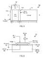
- FIG. 5illustrates the structure and use of the BST-based FBAR (Film Bulk Acoustic Resonator) according to one embodiment of the present invention.
- FIG. 6illustrates the structure of the BST-based FBAR, according to one embodiment of the present invention.
- FIG. 7Aillustrates the structure of the BST-based FBAR, according to another embodiment of the present invention.
- FIG. 7Billustrates the various structures of the acoustic reflector that can be used with the BST-based FBAR of FIG. 7A .
- FIG. 8illustrates the structure of the BST-based FBAR device, according to still another embodiment of the present invention.
- FIG. 9illustrates the simulated behavior of a single BST-based FBAR device in series and shunt configurations.
- FIG. 10Aillustrates a band pass filter circuit implemented using the BST-based FBAR devices according to one embodiment of the present invention.
- FIG. 10Bis a graph illustrating RF transmission measurements, as a function of the frequency of the RF signal, of the band pass filter circuit of FIG. 10A implemented using the BST-based FBAR devices according to one embodiment of the present invention.
- FIG. 10Cis a graph illustrating how the RF transmission measurements of the band pass filter circuit of FIG. 10A implemented using the BST-based FBAR devices change depending upon different DC bias voltages.
- FIG. 11illustrates a duplexer implemented using the BST-based FBAR devices according to one embodiment of the present invention.
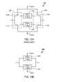
- FIG. 12Aillustrates a conventional switched filter bank.
- FIG. 12Billustrates a switched filter bank implemented using the BST-based FBAR devices according to one embodiment of the present invention.
- BST capacitorscan be configured to exhibit the characteristics of an acoustic resonator if the BST capacitor is appropriately controlled. As the DC bias voltage to BST capacitors is increased, resonant dips in the reflection coefficient are observed. The frequency and depth of the resonance varies with the device area and electrode thicknesses as well as the DC bias voltage. Such resonance in the BST varactors is consistent with a thickness-mode acoustic resonance. BST (and also Strontium Titanate) exhibits a field-induced piezoelectricity, such that under bias the BST thin films can strongly couple electrical energy to acoustic vibration.
- FIG. 2is a graph illustrating RF transmission measurements, of the capacitor 100 using the BST dielectric layer 120 , as a function of the frequency of the RF signal voltage.
- Two curves 210 , 220are shown, corresponding to different applied DC voltages.
- curve 210shows a well-behaved flat response with no significant transmission loss.
- curve 220shows a large resonance and transmission loss appearing at a specific resonant frequency of about 3.7 GHz caused by the piezoelectric effect of the BST material 120 .
- Such piezoelectric effects of the BST dielectric material 120may be used to implement useful electrical components. It is beneficial to control the piezoelectric effects of the BST dielectric material used in varactors to implement useful electronic components.
- FIG. 3is a graph illustrating RF transmission measurements of the BST capacitor of FIG. 1 as a function of the frequency of the RF signal under different DC bias voltages.
- the BST-based varactorshows a well-behaved flat response with no significant transmission loss, as illustrated in curve 310 .
- curve 315shows a large anti-resonance and transmission loss appearing at around 2.55 GHz.
- the curves 320show a large resonance and transmission loss appearing at a certain frequency.
- the BST varactorAt such resonant frequency, the BST varactor is in the high-impedance, anti-resonance state leading to a deep notch in the frequency response.
- the specific frequencies at which the anti-resonance occurincreases as the DC bias voltage increases and the transmission loss at such frequency also increases as the DC bias voltages increase.
- the insertion lossis a function of the capacitive reactance of the BST varactor device. By increasing the device area, it is possible to improve the insertion loss of the off-state and create a more attractive notch filter with a higher loaded Q-factor. Therefore, the BST varactor can be used as a switchable resonator that is switched on with non-zero DC bias voltage but switched off with zero DC-bias voltage.
- the anti-resonant frequency and the transmission losses through the BST varactorcan also be controlled using different levels of the DC bias voltage.
- the BST varactorfunctions as a switchable and adjustable FBAR (Film Bulk Acoustic Resonator) device.
- FIG. 4is a diagram of an equivalent circuit modeling a piezo-electric transducer (acoustic resonator). Such equivalent circuit can also be used to model the piezo-electric characteristics of the BST varactor.
- the transducercan be represented by the KLM (Krimholtz, Leedhom, and Matthaei) model.
- the KLM modeluses an equivalent transmission-line circuit to model the one-dimensional acoustic wave problem. In the KLM model described in FIG.
- Vis the voltage applied to the acoustic resonator
- Iis the current applied to the acoustic resonator
- C cis the clamped capacitance
- Z ais the impedance looking into the acoustic resonator
- 1:nis the turns ratio of a transformer that converts the electrical signal into acoustic resonance
- v 1 and v 2are the particle velocities at the surfaces of the acoustic resonator
- F 1 and F 2are the acoustic forces at the surfaces of the acoustic resonator
- Z 0is the characteristic impedance of the acoustic transmission line
- ⁇is the propagation constant of the acoustic transmission line.
- each acoustic layer(including electrodes, dielectrics, substrates, etc) is specified by a mass density ⁇ m and an acoustic wave velocity ⁇ p , from which equivalent transmission-line parameters (the characteristic impedance Z 0 and propagation constant ⁇ ) can be computed as follows:
- the piezoelectric layer(BST in the present invention) is further characterized by a piezoelectric strain constant d m [C/N] which relates the applied electric field to the resulting mechanical strain (deformation). It can be shown that the remaining equivalent circuit parameters in the KLM model are given by:
- piezoelectric materialsare often characterized by a dimensionless piezoelectric coupling constant K 2 , or the electromechanical coupling constant k t 2 , related by
- FIG. 5illustrates the structure and use of the BST-based FBAR 500 according to one embodiment of the present invention.
- the BST-based FBAR device 500includes a BST (e.g., Ba x Sr 1-x TiO 3 ) layer 520 disposed between a top electrode 510 a and a bottom electrode 510 b supported by a substrate 530 (e.g., Sapphire).
- the substrate material 530is not limited to Sapphire and other materials such as Silicon can be used suitably.
- the top electrode 510 a , the BST layer 520 , the bottom electrode 510 b , and the substrate 530has a thickness of t 1 , t 2 , t 3 , and t 4 , respectively.
- the BST-based FBAR device 500illustrates the characteristics of an FBAR device under non-zero DC bias voltage.
- a voltage V g 540(including a DC component and an AC component) is applied to the electrodes 510 a , 510 b through the input impedance Z g .
- a DC voltage generating an electric field of 1 MV/cm across the FBAR device 500can change the dielectric constant of the BST material 520 by factors of 2 to 3, leading to different frequency responses of the FBAR device 500 as illustrated in FIG. 4 .
- the FBAR device 500loses the characteristics of an FBAR, and has characteristics similar to a simple thin film capacitor.
- FIG. 6illustrates the structure of the BST-based FBAR 600 , according to one embodiment of the present invention.
- the FBAR 600is fabricated on a sapphire substrate 530 , and includes top and bottom electrodes 510 a , 510 b and a BST layer 520 disposed between the top and bottom electrodes 510 a , 510 b .
- the substrate material 530is not limited to Sapphire and other materials such as Silicon can be used suitably.
- the FBAR 600 deviceis formed over air 620 such that there is an air gap 620 between the bottom electrode 510 b and the sapphire substrate 530 .
- the air gap 620reduces the damping of the resonance caused by the substrate 530 .
- DC bias 650is applied to the top electrode 510 a , and the bottom electrode 510 b is connected to DC ground 651 .
- the RF signal 652is input to the top electrode 510 a , passes through the BST layer 520 , and is output 654 from the bottom electrode 510 b.
- FIG. 7Aillustrates the structure of the BST-based FBAR 700 , according to another embodiment of the present invention.
- the FBAR 700is fabricated on a sapphire substrate 530 , and includes top and bottom electrodes 510 a , 510 b and a BST layer 520 disposed between the top and bottom electrodes 510 a , 510 b .
- the substrate material 530is not limited to Sapphire and other materials such as Silicon can be used suitably.
- the FBAR 700 device in FIG. 7Ais fabricated on an acoustic reflector 705 which is disposed on the sapphire substrate 530 .
- the acoustic reflector 705(also referred to as an “acoustic mirror”) functions to reduce the damping of the resonance caused by the substrate 530 , as will be explained in more detail with reference to FIG. 7B .
- DC bias 780is applied to the top electrode 510 a , and the bottom electrode 510 b is connected to DC ground 781 .
- the RF signal 782is input to the top electrode 510 a , passes through the BST layer 520 , and is output 784 from the bottom electrode 510 b.
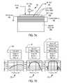
- FIG. 7Billustrates the various structures of the acoustic reflector 705 that can be used in the BST-based FBAR 700 of FIG. 7A .
- the acoustic reflector 705is made from alternating quarter-wavelength layers of high and low acoustic impedance materials.
- the acoustic impedanceis related to the mass-density and sound velocity of the materials.
- platinum (Pt) layersare highly desirable because Pt is refractory (can withstand high BST deposition temperatures), resistant to oxidation, and has a large work function, forming a large Schottky barrier at the interface to reduce leakage.
- FIG. 7Bshows the improvement in reflection coefficient for three simple acoustic mirror stacks 750 , 760 , 770 .
- the acoustic reflector 750has a simple Pt electrode disposed on a sapphire substrate, showing a reflection coefficient as in graph 752 .
- the acoustic reflector 760has a 2-layer Pt/SiO 2 mirror disposed on a sapphire substrate, showing a reflection coefficient as in graph 762 .
- the acoustic reflector 770has a 4-layer Pt/SiO 2 mirror disposed on a sapphire substrate, showing a reflection coefficient as in graph 772 .
- the layer thicknesseswere chosen to be a quarter-wavelength at 2.5 GHz. It can be seen the reflection coefficient improves as the acoustic reflector has multiple Pt/SiO 2 layers as in the acoustic mirror 760 , 770 .
- FIG. 8illustrates the structure of the BST-based FBAR device 800 , according to still another embodiment of the present invention.
- the FBAR 800is fabricated on a sapphire substrate 830 , and includes top and bottom electrodes 510 a , 510 b and a BST layer 520 disposed between the top and bottom electrodes 510 a , 510 b .
- the substrate material 530is not limited to Sapphire and other materials such as Silicon can be used suitably.
- the sapphire substrate 830has a pair of tapered parts (tapered as they become further away from the bottom electrode 510 b ) with an air gap 820 disposed between the pair of tapered parts of the sapphire substrate 830 .
- the via 860provides a conduit for electrical connection to the bottom electrode 510 b .
- DC bias 850is applied to the top electrode 510 a , and the bottom electrode 510 b is connected to DC ground 851 .
- the RF signal 852is input to the top electrode 510 a , passes through the BST layer 520 , and is output 854 from the bottom electrode 510 b.
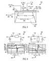
- FIG. 9illustrates the simulated behavior of a single BST-based FBAR device in series 900 and shunt 950 configurations.
- a clear way to exploit the voltage-dependent piezoelectric coupling of the BST-based FBAR devicesis by designing the circuits to maximize the impedance differential between “off” (zero bias) and “on” (maximum bias) states.
- the series configuration 900includes the FBAR device 902 in series with an input impedance 904 (Z 0 ) receiving an input RF input signal 908 and an output impedance 906 (Z 0 ) for the RF output signal.
- the shunt configuration 950includes an input impedance 918 (Z 0 ) receiving an RF input signal 918 , and the FBAR device 912 in parallel with the output impedance 916 (Z 0 ) for the RF output signal.
- the anti-resonancealso occurs around 2.55 GHz when a DC bias of 40 V is applied to the FBAR device 912 , while no anti-resonance occurs when no DC bias is applied (0 Volt).
- the simulations in FIG. 9include electrical losses associated with the material loss tangent and series resistance of the electrodes, as well as mechanical damping and acoustic losses in the electrodes and substrates of the FBAR devices 902 , 912 . Further improvements in performance can be obtained by using more advanced acoustic mirror stacks and higher-quality BST films.
- BST filmsare usually engineered for high-tunability at the expense of higher loss tangents; in this application, BST composition and deposition conditions could be optimized purely for low loss tangents, since a large capacitive tunability is not necessary for the proper functioning of these devices.
- the switched and tunable resonance properties of the BST-based FBAR devicescan be used in modern communication systems where frequency-agile or reconfigurable components are becoming increasingly important and necessary to cope with a multitude of signal frequencies and modulation formats, including analog front-end components near the antenna, such as filters, duplexers, antenna and amplifier matching networks, etc.
- analog front-end components near the antennasuch as filters, duplexers, antenna and amplifier matching networks, etc.
- This is a difficult problem area for electronicsbecause the transmit power levels and associated RF voltage swings can be quite large, raising breakdown and linearity concerns, while at the same time the receive signal levels are extremely low, placing a premium on insertion loss to maintain an acceptable signal-to-noise ratio.
- the BST-based FBAR devices according to the present inventionare switchable and tunable, they are functionally equivalent to a high-selectivity filter and a low-loss switch, where the switch draws no DC power.
- An array of such filterscould implement a very compact and reconfigurable high-selectivity filter bank.
- BST-based FBARscould be combined to make a low-loss and high-selectivity duplexer or TR switch. There are many other possibilities for frequency-agile components.
- FIG. 10Aillustrates a band pass filter circuit implemented using the BST-based FBAR devices according to one embodiment of the present invention.
- the “ladder” filter network shown in FIG. 10Aincludes capacitors 1004 , 1006 , 1008 and BST-based FBAR devices 1010 , 1012 , receiving an RF input signal through an input impedance 1002 and generating an RF output signal across the output impedance 1014 .
- the BST-based FBAR devices 1010 , 1012may be of any configuration as illustrated in FIGS. 5 , 6 , 7 A, or 8 .
- the “ladder” filter network shown in FIG. 10Ais essentially a combination of capacitively-coupled shunt resonators, and can be optimized using classical filter techniques.
- FIG. 10Bis a graph illustrating RF transmission simulation results, as a function of the frequency of the RF signal, of the band pass filter circuit implemented using the BST-based FBAR devices according to one embodiment of the present invention in FIG. 10A . It is apparent that the filter network of FIG. 10A exhibits the characteristics of a 2-pole band pass filter when a DC bias of 40 V is applied to the FBAR devices 1010 , 1012 but that a steady frequency response occurs when the DC bias is off (0 volt). In this simple filter network with only two BST FBAR devices 1010 , 1012 , over a 40 dB on-off dynamic range can be obtained, with less than 3 dB insertion loss.
- FIG. 10Cis a graph illustrating how the RF transmission measurements of the band pass filter circuit implemented using the BST-based FBAR devices as in FIG. 10A change depending upon different DC bias voltages applied to the BST-based FBAR devices.
- the DC bias voltage applied to the BST-based FBAR devices 1010 , 1012is V 1
- the center frequency of the band pass filteris positioned at F 1 .
- the filter responseshifts upwards and settles at the new center frequency of F 2 . Therefore, the filter of FIG.
- the filter of FIG. 10Ais not only switchable based on whether a DC bias voltage is applied, but its frequency response is also tunable based on the level of the DC bias voltage.
- the filter of FIG. 10Aessentially has multiple frequency bands. For example, a DC bias voltage of V 1 applied to the filter network would enable operation of Band 1 centered at F 1 while suppressing Band 2 centered at V 2 . Conversely, a DC bias voltage of V 2 would enable Band 2 centered at F 2 while disabling Band 1 centered at F 1 .
- FIG. 11illustrates a duplexer 1100 implemented using the BST-based FBAR devices according to one embodiment of the present invention.
- the duplexer 1100includes two BST-based FBAR filter circuits 1106 , 1008 , such as those shown in FIG. 10A , to route signals between the antenna 1110 and the transmit (Tx) block 1102 or the receive (Rx) block 1104 .
- the BST-based FBAR filter 1106 in the transmit pathis activated by applying a non-zero DC bias voltage (V switch ) to the BST-based FBAR 1106 , the BST-based FBAR filter 1108 in the receive path is turned off, thus isolating the receiver 1104 from the transmit signal 1102 .
- V switchnon-zero DC bias voltage
- the BST-based FBAR filter 1108 in the receive pathis activated by applying a non-zero DC bias voltage ( ⁇ V switch ) to the BST-based FBAR 1108
- the BST-based FBAR filter 1106 in the transmit pathis turned off, thus isolating the transmitter 1102 from the receive signal 1104 .
- a duplexer functionalitycan be implemented using filters with different pass band frequencies for the Tx and Rx paths, by applying different DC bias voltages to the BST-based FBAR filters 1106 , 1108 .
- FIG. 12Aillustrates a conventional switched filter bank 1200 , including conventional FBAR switches 1202 , 1204 .
- the conventional FBAR switches 1202 , 1204are not independently switchable, and thus the DC switching signals (V switch and ⁇ V switch ) are applied to the switches 1210 , 1212 , 1214 , 1216 to externally turn on or off the conventional FBAR filters 1202 , 1204 .
- FIG. 12Billustrates a switched filter bank 1250 implemented using the BST-based FBAR devices according to one embodiment of the present invention.
- the filter bank 1250includes two BST-based FBAR filters 1252 , 1254 .
- the BST-based FBAR filters 1252 , 1254are switched directly by the DC switching signals (V switch and ⁇ V switch ) because the BST-based FBAR filters 1252 , 1254 are switchable based on whether a DC bias signal is applied thereto.
- the switched filter bank 1250does not require external switches to switch on or off the BST-based FBAR filters 1252 , 1254 .
Landscapes
- Physics & Mathematics (AREA)
- Acoustics & Sound (AREA)
- Chemical & Material Sciences (AREA)
- Engineering & Computer Science (AREA)
- Ceramic Engineering (AREA)
- Piezo-Electric Or Mechanical Vibrators, Or Delay Or Filter Circuits (AREA)
Abstract
Description
where A is the active device area (electrode area) and ω is the frequency of resonance. The acoustic loss in each layer is specified by a mechanical viscosity η, such that the attenuation factor α is given by
and each layer is defined by a complex propagation constant γ=α+jβ. In addition to these parameters, the piezoelectric layer (BST in the present invention) is further characterized by a piezoelectric strain constant dm[C/N] which relates the applied electric field to the resulting mechanical strain (deformation). It can be shown that the remaining equivalent circuit parameters in the KLM model are given by:
and l is the length of the acoustic transmission line, and cmis the stiffness constant, related to the mass density and acoustic velocity as cm=ρmνp2. Note that ∈ is the permittivity of the material with no mechanical stress, and ∈sis the permittivity that would be measured if the material were clamped to prevent deformation. Since the piezoelectric strain constant often appears in combination with other parameters, piezoelectric materials are often characterized by a dimensionless piezoelectric coupling constant K2, or the electromechanical coupling constant kt2, related by
These formulas are convenient for calculations related to complex multi-layered structures.
Claims (16)
Priority Applications (6)
| Application Number | Priority Date | Filing Date | Title |
|---|---|---|---|
| US11/682,252US7675388B2 (en) | 2006-03-07 | 2007-03-05 | Switchable tunable acoustic resonator using BST material |
| EP07757969AEP1992023B1 (en) | 2006-03-07 | 2007-03-06 | Duplexer and filter bank, comprising switchable tunable acoustic resonator using BST material |
| PCT/US2007/063372WO2007103912A2 (en) | 2006-03-07 | 2007-03-06 | Switchable tunable acoustic resonator using bst material |
| ES07757969TES2395974T3 (en) | 2006-03-07 | 2007-03-06 | Duplexer and filter bank, comprising a switchable tunable acoustic resonator that uses BST material |
| JP2008558502AJP2009529833A (en) | 2006-03-07 | 2007-03-06 | Switchable and tunable acoustic resonator using BST material |
| US12/690,415US8130058B2 (en) | 2006-03-07 | 2010-01-20 | Switchable tunable acoustic resonator using BST material |
Applications Claiming Priority (3)
| Application Number | Priority Date | Filing Date | Title |
|---|---|---|---|
| US78022906P | 2006-03-07 | 2006-03-07 | |
| US83525306P | 2006-08-02 | 2006-08-02 | |
| US11/682,252US7675388B2 (en) | 2006-03-07 | 2007-03-05 | Switchable tunable acoustic resonator using BST material |
Related Child Applications (1)
| Application Number | Title | Priority Date | Filing Date |
|---|---|---|---|
| US12/690,415ContinuationUS8130058B2 (en) | 2006-03-07 | 2010-01-20 | Switchable tunable acoustic resonator using BST material |
Publications (2)
| Publication Number | Publication Date |
|---|---|
| US20070210879A1 US20070210879A1 (en) | 2007-09-13 |
| US7675388B2true US7675388B2 (en) | 2010-03-09 |
Family
ID=38475793
Family Applications (2)
| Application Number | Title | Priority Date | Filing Date |
|---|---|---|---|
| US11/682,252Expired - Fee RelatedUS7675388B2 (en) | 2006-03-07 | 2007-03-05 | Switchable tunable acoustic resonator using BST material |
| US12/690,415Expired - Fee RelatedUS8130058B2 (en) | 2006-03-07 | 2010-01-20 | Switchable tunable acoustic resonator using BST material |
Family Applications After (1)
| Application Number | Title | Priority Date | Filing Date |
|---|---|---|---|
| US12/690,415Expired - Fee RelatedUS8130058B2 (en) | 2006-03-07 | 2010-01-20 | Switchable tunable acoustic resonator using BST material |
Country Status (5)
| Country | Link |
|---|---|
| US (2) | US7675388B2 (en) |
| EP (1) | EP1992023B1 (en) |
| JP (1) | JP2009529833A (en) |
| ES (1) | ES2395974T3 (en) |
| WO (1) | WO2007103912A2 (en) |
Cited By (18)
| Publication number | Priority date | Publication date | Assignee | Title |
|---|---|---|---|---|
| US20100109808A1 (en)* | 2006-03-07 | 2010-05-06 | Agile Rf, Inc. | Switchable Tunable Acoustic Resonator Using BST Material |
| US20100213606A1 (en)* | 2009-02-24 | 2010-08-26 | Sun Microsystems, Inc. | Dielectric enhancements to chip-to-chip capacitive proximity communication |
| US8648671B2 (en) | 2010-09-01 | 2014-02-11 | Samsung Electronics Co., Ltd. | Bulk acoustic wave resonator structure, a manufacturing method thereof, and a duplexer using the same |
| US20140085020A1 (en)* | 2012-09-27 | 2014-03-27 | Commissariat A L'energie Atomique Et Aux Energies Alternatives | Acoustic structure comprising at least one resonator and at least one cointegrated capacitor in one and the same piezoelectric or ferroelectric layer |
| US9054671B2 (en) | 2011-11-09 | 2015-06-09 | International Business Machines Corporation | Tunable filter structures and design structures |
| US9374059B1 (en)* | 2015-01-06 | 2016-06-21 | Zhuhai Advanced Chip Carriers & Electronic Substrate Solutions Technologies Co. Ltd. | Film bulk acoustic resonator filter |
| US20170111021A1 (en)* | 2015-10-14 | 2017-04-20 | Qorvo Us, Inc. | Methods for fabricating acoustic structure with inclined c-axis piezoelectric bulk and crystalline seed layers |
| US9880675B2 (en) | 2012-04-13 | 2018-01-30 | Apple Inc. | Capacitive sensing array modulation |
| US9883822B2 (en) | 2013-06-05 | 2018-02-06 | Apple Inc. | Biometric sensor chip having distributed sensor and control circuitry |
| US20180141800A1 (en)* | 2015-03-13 | 2018-05-24 | Taiwan Semiconductor Manufacturing Co., Ltd. | Mems transducer and method for manufacturing the same |
| US9984270B2 (en) | 2013-08-05 | 2018-05-29 | Apple Inc. | Fingerprint sensor in an electronic device |
| US10007833B2 (en) | 2012-05-18 | 2018-06-26 | Apple Inc. | Capacitive sensor packaging |
| US10284355B2 (en) | 2015-06-25 | 2019-05-07 | Samsung Electronics Co., Ltd. | Communication device and electronic device including the same |
| US10571437B2 (en) | 2015-12-15 | 2020-02-25 | Qorvo Us, Inc. | Temperature compensation and operational configuration for bulk acoustic wave resonator devices |
| US10628654B2 (en) | 2013-09-09 | 2020-04-21 | Apple Inc. | Capacitive sensing array having electrical isolation |
| US11381212B2 (en) | 2018-03-21 | 2022-07-05 | Qorvo Us, Inc. | Piezoelectric bulk layers with tilted c-axis orientation and methods for making the same |
| US11401601B2 (en) | 2019-09-13 | 2022-08-02 | Qorvo Us, Inc. | Piezoelectric bulk layers with tilted c-axis orientation and methods for making the same |
| US11824511B2 (en) | 2018-03-21 | 2023-11-21 | Qorvo Us, Inc. | Method for manufacturing piezoelectric bulk layers with tilted c-axis orientation |
Families Citing this family (12)
| Publication number | Priority date | Publication date | Assignee | Title |
|---|---|---|---|---|
| US8198958B1 (en)* | 2009-03-30 | 2012-06-12 | Triquint Semiconductor, Inc. | Power amplifier matching RF system and method using bulk acoustics wave device |
| EP2436049B1 (en)* | 2009-05-28 | 2019-05-01 | Northrop Grumman Systems Corporation | Lateral over-moded bulk acoustic resonators |
| RU2397607C1 (en)* | 2009-07-17 | 2010-08-20 | Государственное образовательное учреждение высшего профессионального образования "Санкт-Петербургский государственный электротехнический университет "ЛЭТИ" | Ferroelectric acoustic resonator and tuning method of its resonance frequency |
| CN104966864B (en)* | 2009-11-02 | 2018-03-06 | 株式会社 Kmw | Radio-frequency filter |
| FR2962613B1 (en)* | 2010-07-06 | 2013-08-16 | Commissariat Energie Atomique | DEVICE FOR IMPEDANCE ADAPTATION OF A COMPONENT COMPRISING AN ADAPTABLE IMPEDANCE FILTER BASED ON PEROVSKITE MATERIAL |
| KR101868988B1 (en) | 2011-08-05 | 2018-06-20 | 삼성전자주식회사 | Bulk acoustic wave resonator |
| FR3016707A1 (en)* | 2014-01-23 | 2015-07-24 | St Microelectronics Tours Sas | CONTROL CIRCUIT FOR A POLARIZABLE ADJUSTABLE CAPACITOR CAPACITOR |
| US10205436B2 (en)* | 2016-09-30 | 2019-02-12 | Qorvo Us, Inc. | High-voltage converter based tuning of acoustic filters |
| US10263601B2 (en)* | 2016-10-31 | 2019-04-16 | Avago Technologies International Sales Pte. Limited | Tunable bulk acoustic resonator device with improved insertion loss |
| US10601397B2 (en)* | 2017-03-24 | 2020-03-24 | Zhuhai Crystal Resonance Technologies Co., Ltd. | RF resonator electrode and membrane combinations and method of fabrication |
| US11146235B1 (en)* | 2020-05-15 | 2021-10-12 | Qorvo Us, Inc. | Tunable BAW resonator with ion-conductible structure |
| US12170515B2 (en) | 2022-01-31 | 2024-12-17 | Qorvo Us, Inc. | Reversed semilattice filter |
Citations (34)
| Publication number | Priority date | Publication date | Assignee | Title |
|---|---|---|---|---|
| US2802171A (en) | 1955-11-10 | 1957-08-06 | Mc Graw Edison Co | Arrangement for switching capacitors |
| US3562637A (en) | 1969-07-07 | 1971-02-09 | Us Army | Low voltage dc control of voltage-variable capacitors |
| US5273609A (en) | 1990-09-12 | 1993-12-28 | Texas Instruments Incorporated | Method and apparatus for time-division plasma chopping in a multi-channel plasma processing equipment |
| US5382930A (en)* | 1992-12-21 | 1995-01-17 | Trw Inc. | Monolithic multipole filters made of thin film stacked crystal filters |
| US5489548A (en) | 1994-08-01 | 1996-02-06 | Texas Instruments Incorporated | Method of forming high-dielectric-constant material electrodes comprising sidewall spacers |
| US5593914A (en) | 1996-03-19 | 1997-01-14 | Radiant Technologies, Inc. | Method for constructing ferroelectric capacitor-like structures on silicon dioxide surfaces |
| US5714917A (en) | 1996-10-02 | 1998-02-03 | Nokia Mobile Phones Limited | Device incorporating a tunable thin film bulk acoustic resonator for performing amplitude and phase modulation |
| US5721700A (en) | 1996-01-26 | 1998-02-24 | Nec Corporation | Non-volatile semiconductor memory device in which applied voltage to ferroelectric capacitor is adjusted |
| US5790367A (en) | 1995-12-12 | 1998-08-04 | U.S. Philips Corporation | Multilayer capacitor comprising a dielectric of modified barium strontium titanate |
| US6077737A (en) | 1998-06-02 | 2000-06-20 | Mosel Vitelic, Inc. | Method for forming a DRAM having improved capacitor dielectric layers |
| US6222245B1 (en) | 1995-10-31 | 2001-04-24 | Sgs-Thomson Microelectronics S.R.L. | High capacity capacitor and corresponding manufacturing process |
| US6300654B1 (en) | 1999-04-30 | 2001-10-09 | Stmicroelectronics S.R.L. | Structure of a stacked memory cell, in particular a ferroelectric cell |
| US20010028285A1 (en) | 2000-04-06 | 2001-10-11 | Klee Mareike Katharine | Tunable filter arrangement comprising resonators |
| US20010048352A1 (en) | 2000-04-06 | 2001-12-06 | Klee Mareike Katharine | Tunable filter arrangement |
| US6377440B1 (en) | 2000-09-12 | 2002-04-23 | Paratek Microwave, Inc. | Dielectric varactors with offset two-layer electrodes |
| US6383858B1 (en) | 2000-02-16 | 2002-05-07 | Agere Systems Guardian Corp. | Interdigitated capacitor structure for use in an integrated circuit |
| US6432794B1 (en) | 1999-11-26 | 2002-08-13 | Worldwide Semiconductor Manufacturing Corp. | Process for fabricating capacitor |
| US6451665B1 (en) | 1998-12-11 | 2002-09-17 | Hitachi, Ltd. | Method of manufacturing a semiconductor integrated circuit |
| US6452776B1 (en) | 2000-04-06 | 2002-09-17 | Intel Corporation | Capacitor with defect isolation and bypass |
| US6503792B2 (en) | 1999-12-28 | 2003-01-07 | Infincon Technologies Ag | Method for fabricating a patterned metal-oxide-containing layer |
| US20030067023A1 (en) | 2001-10-09 | 2003-04-10 | Koninklijke Philips Electronics N.V. | Metal-insulator-metal (MIM) capacitor structure and methods of fabricating same |
| US6646499B2 (en) | 2000-05-05 | 2003-11-11 | Infineon Technologies Ag | Voltage-controlled capacitor |
| US6683341B1 (en) | 2001-12-05 | 2004-01-27 | Agile Materials & Technologies, Inc. | Voltage-variable capacitor with increased current conducting perimeter |
| US20040087082A1 (en) | 2000-12-11 | 2004-05-06 | Murata Manufacturing Co.,Ltd. | Mim capacitor and manufacturing method thereor |
| US6737930B2 (en) | 2001-04-11 | 2004-05-18 | Kyocera Wireless Corp. | Tunable planar capacitor |
| US6768396B2 (en)* | 1999-12-22 | 2004-07-27 | Koninklijke Philips Electronics N.V. | Filter arrangement |
| US20040164367A1 (en) | 2003-02-21 | 2004-08-26 | Jae-Yeong Park | Duplexer filter having film bulk acoustic resonator and semiconductor package thereof |
| US20040212277A1 (en) | 2001-07-03 | 2004-10-28 | Ralph Stommer | Frequency-tunable resonator |
| US20040259316A1 (en) | 2001-12-05 | 2004-12-23 | Baki Acikel | Fabrication of parallel plate capacitors using BST thin films |
| US6847271B2 (en) | 2000-09-25 | 2005-01-25 | Siemens Aktiengesellschaft | Component having an acoustically active material for tuning during operation |
| US6924583B2 (en) | 2002-05-03 | 2005-08-02 | Asia Pacific Microsystems, Inc. | Film bulk acoustic device with integrated tunable and trimmable device |
| US7042701B2 (en) | 2003-08-05 | 2006-05-09 | Impinj, Inc. | High-voltage CMOS-compatible capacitors |
| US7098575B2 (en)* | 2003-04-21 | 2006-08-29 | Hrl Laboratories, Llc | BAW device and method for switching a BAW device |
| US20080129416A1 (en) | 2006-08-28 | 2008-06-05 | Stmicroelectronics Sa | Switchable filter with resonators |
Family Cites Families (12)
| Publication number | Priority date | Publication date | Assignee | Title |
|---|---|---|---|---|
| JP2830556B2 (en)* | 1991-12-06 | 1998-12-02 | 株式会社村田製作所 | Polarization method of piezoelectric body |
| FI106894B (en)* | 1998-06-02 | 2001-04-30 | Nokia Mobile Phones Ltd | resonator structures |
| JP3949990B2 (en)* | 2002-03-29 | 2007-07-25 | 株式会社東芝 | Voltage controlled oscillator |
| JP3854212B2 (en)* | 2002-03-29 | 2006-12-06 | 株式会社東芝 | High frequency filter |
| JP2004304704A (en)* | 2003-04-01 | 2004-10-28 | Matsushita Electric Ind Co Ltd | Thin film acoustic resonator and thin film acoustic resonator circuit |
| JP2005109573A (en)* | 2003-09-26 | 2005-04-21 | Kyocera Corp | Resonator and electronic equipment |
| CN100583626C (en)* | 2003-10-06 | 2010-01-20 | Nxp股份有限公司 | Resonator structure and method of producing it |
| FR2864727B1 (en)* | 2003-12-29 | 2007-05-11 | St Microelectronics Sa | ELECTRONIC CIRCUIT COMPRISING A RESONATOR INTENDED TO BE INTEGRATED IN A SEMICONDUCTOR PRODUCT |
| WO2006004470A1 (en)* | 2004-07-06 | 2006-01-12 | Telefonaktiebolaget Lm Ericsson (Publ) | A tuneable resonator |
| US7615833B2 (en)* | 2004-07-13 | 2009-11-10 | Avago Technologies Wireless Ip (Singapore) Pte. Ltd. | Film bulk acoustic resonator package and method of fabricating same |
| JP2008515998A (en) | 2004-10-13 | 2008-05-15 | スミスクライン ビーチャム コーポレーション | Compound |
| US7675388B2 (en)* | 2006-03-07 | 2010-03-09 | Agile Rf, Inc. | Switchable tunable acoustic resonator using BST material |
- 2007
- 2007-03-05USUS11/682,252patent/US7675388B2/ennot_activeExpired - Fee Related
- 2007-03-06JPJP2008558502Apatent/JP2009529833A/enactivePending
- 2007-03-06WOPCT/US2007/063372patent/WO2007103912A2/enactiveApplication Filing
- 2007-03-06EPEP07757969Apatent/EP1992023B1/ennot_activeNot-in-force
- 2007-03-06ESES07757969Tpatent/ES2395974T3/enactiveActive
- 2010
- 2010-01-20USUS12/690,415patent/US8130058B2/ennot_activeExpired - Fee Related
Patent Citations (34)
| Publication number | Priority date | Publication date | Assignee | Title |
|---|---|---|---|---|
| US2802171A (en) | 1955-11-10 | 1957-08-06 | Mc Graw Edison Co | Arrangement for switching capacitors |
| US3562637A (en) | 1969-07-07 | 1971-02-09 | Us Army | Low voltage dc control of voltage-variable capacitors |
| US5273609A (en) | 1990-09-12 | 1993-12-28 | Texas Instruments Incorporated | Method and apparatus for time-division plasma chopping in a multi-channel plasma processing equipment |
| US5382930A (en)* | 1992-12-21 | 1995-01-17 | Trw Inc. | Monolithic multipole filters made of thin film stacked crystal filters |
| US5489548A (en) | 1994-08-01 | 1996-02-06 | Texas Instruments Incorporated | Method of forming high-dielectric-constant material electrodes comprising sidewall spacers |
| US6222245B1 (en) | 1995-10-31 | 2001-04-24 | Sgs-Thomson Microelectronics S.R.L. | High capacity capacitor and corresponding manufacturing process |
| US5790367A (en) | 1995-12-12 | 1998-08-04 | U.S. Philips Corporation | Multilayer capacitor comprising a dielectric of modified barium strontium titanate |
| US5721700A (en) | 1996-01-26 | 1998-02-24 | Nec Corporation | Non-volatile semiconductor memory device in which applied voltage to ferroelectric capacitor is adjusted |
| US5593914A (en) | 1996-03-19 | 1997-01-14 | Radiant Technologies, Inc. | Method for constructing ferroelectric capacitor-like structures on silicon dioxide surfaces |
| US5714917A (en) | 1996-10-02 | 1998-02-03 | Nokia Mobile Phones Limited | Device incorporating a tunable thin film bulk acoustic resonator for performing amplitude and phase modulation |
| US6077737A (en) | 1998-06-02 | 2000-06-20 | Mosel Vitelic, Inc. | Method for forming a DRAM having improved capacitor dielectric layers |
| US6451665B1 (en) | 1998-12-11 | 2002-09-17 | Hitachi, Ltd. | Method of manufacturing a semiconductor integrated circuit |
| US6300654B1 (en) | 1999-04-30 | 2001-10-09 | Stmicroelectronics S.R.L. | Structure of a stacked memory cell, in particular a ferroelectric cell |
| US6432794B1 (en) | 1999-11-26 | 2002-08-13 | Worldwide Semiconductor Manufacturing Corp. | Process for fabricating capacitor |
| US6768396B2 (en)* | 1999-12-22 | 2004-07-27 | Koninklijke Philips Electronics N.V. | Filter arrangement |
| US6503792B2 (en) | 1999-12-28 | 2003-01-07 | Infincon Technologies Ag | Method for fabricating a patterned metal-oxide-containing layer |
| US6383858B1 (en) | 2000-02-16 | 2002-05-07 | Agere Systems Guardian Corp. | Interdigitated capacitor structure for use in an integrated circuit |
| US20010048352A1 (en) | 2000-04-06 | 2001-12-06 | Klee Mareike Katharine | Tunable filter arrangement |
| US20010028285A1 (en) | 2000-04-06 | 2001-10-11 | Klee Mareike Katharine | Tunable filter arrangement comprising resonators |
| US6452776B1 (en) | 2000-04-06 | 2002-09-17 | Intel Corporation | Capacitor with defect isolation and bypass |
| US6646499B2 (en) | 2000-05-05 | 2003-11-11 | Infineon Technologies Ag | Voltage-controlled capacitor |
| US6377440B1 (en) | 2000-09-12 | 2002-04-23 | Paratek Microwave, Inc. | Dielectric varactors with offset two-layer electrodes |
| US6847271B2 (en) | 2000-09-25 | 2005-01-25 | Siemens Aktiengesellschaft | Component having an acoustically active material for tuning during operation |
| US20040087082A1 (en) | 2000-12-11 | 2004-05-06 | Murata Manufacturing Co.,Ltd. | Mim capacitor and manufacturing method thereor |
| US6737930B2 (en) | 2001-04-11 | 2004-05-18 | Kyocera Wireless Corp. | Tunable planar capacitor |
| US20040212277A1 (en) | 2001-07-03 | 2004-10-28 | Ralph Stommer | Frequency-tunable resonator |
| US20030067023A1 (en) | 2001-10-09 | 2003-04-10 | Koninklijke Philips Electronics N.V. | Metal-insulator-metal (MIM) capacitor structure and methods of fabricating same |
| US6683341B1 (en) | 2001-12-05 | 2004-01-27 | Agile Materials & Technologies, Inc. | Voltage-variable capacitor with increased current conducting perimeter |
| US20040259316A1 (en) | 2001-12-05 | 2004-12-23 | Baki Acikel | Fabrication of parallel plate capacitors using BST thin films |
| US6924583B2 (en) | 2002-05-03 | 2005-08-02 | Asia Pacific Microsystems, Inc. | Film bulk acoustic device with integrated tunable and trimmable device |
| US20040164367A1 (en) | 2003-02-21 | 2004-08-26 | Jae-Yeong Park | Duplexer filter having film bulk acoustic resonator and semiconductor package thereof |
| US7098575B2 (en)* | 2003-04-21 | 2006-08-29 | Hrl Laboratories, Llc | BAW device and method for switching a BAW device |
| US7042701B2 (en) | 2003-08-05 | 2006-05-09 | Impinj, Inc. | High-voltage CMOS-compatible capacitors |
| US20080129416A1 (en) | 2006-08-28 | 2008-06-05 | Stmicroelectronics Sa | Switchable filter with resonators |
Non-Patent Citations (33)
| Title |
|---|
| Acikel, Baki et al., "A New High Performance Phase Shifter using BaxSr1-x TiO3 Thin Films," IEEE Microwave and Wireless Components Letters, vol. 12, No. 7, Jul. 2002, pp. 237-239. |
| Acikel, Baki et al., "BST Varactor Design and Fabrication," project funded by DARPA FAME Program, 1 page [online], [retrieved on Jun. 28, 2004]. Retrieved from the Internet . |
| Acikel, Baki et al., "BST Varactor Design and Fabrication," project funded by DARPA FAME Program, 1 page [online], [retrieved on Jun. 28, 2004]. Retrieved from the Internet <URL: http://my.ece.ucsb.edu/yorklab/Projects/Ferroelectrics/Devices/bstdevicedesign.htm>. |
| Acikel, Baki et al., "Overview of Program," DARPA FAME Program, 8 pages [online], [retrieved on Jun. 23, 2004]. Retrieved from the Internet . |
| Acikel, Baki et al., "Overview of Program," DARPA FAME Program, 8 pages [online], [retrieved on Jun. 23, 2004]. Retrieved from the Internet <URL: http://my.ece.ucsb.edu/yorklab/Projects/Ferroelectrics/Devices/DeviceDesign.pdf>. |
| Acikel, Baki et al., "Technology Comparison," DARPA FAME Program, 6 pages [online], [retrieved on Jun. 23, 2004]. Retrieved from the Internet . |
| Acikel, Baki et al., "Technology Comparison," DARPA FAME Program, 6 pages [online], [retrieved on Jun. 23, 2004]. Retrieved from the Internet <URL: http://my.ece.ucsb.edu/yorklab/Projects/Ferroelectrics/Devices/VaractorComparison.pdf>. |
| Erker, Erich G. et al., "Monolithic Ka-Band Phase Shifter Using Voltage Tunable BaSrTiO3 Parallel Plate Capacitors," IEEE Microwave and Guided Wave Letters, vol. 10, No. 1, Jan. 2000, pp. 10-12. |
| Liu, Yu et al., "BaSrTioO3 Interdigitated Capacitors for Distributed Phase Shifter Applications," 2000, IEEE Microwave and Guided Wave Letters, vol. 10, No. 11, Nov. 2000, pp. 448-450. |
| Liu, Yu et al., "High-performance and Low-cost Distributed Phase Shifters Using Optimized BaSrTiO3 Interdigitated Capacitors," Electrical and Computer Engineering Dept., Materials Dept., University of California at Santa Barbara, Santa Barbara, CA 93106, 14 pages [online], [retrieved on Jun. 24, 2003]. Retrieved from the Internet . |
| Liu, Yu et al., "High-performance and Low-cost Distributed Phase Shifters Using Optimized BaSrTiO3 Interdigitated Capacitors," Electrical and Computer Engineering Dept., Materials Dept., University of California at Santa Barbara, Santa Barbara, CA 93106, 14 pages [online], [retrieved on Jun. 24, 2003]. Retrieved from the Internet <URL: http://my.ece.ucsb.edu/yorklab/Publications/pubs.htm>. |
| Nagra, Amit S. et al., "Distributed Analog Phase Shifters with Low Insertion Loss," IEEE Transactions on Microwave Theory and Techniques, vol. 47, No. 9, Sep. 1999, pp. 1705-1711. |
| Padmini, P. et al., "Realization of High Tunability Barium Strontium Titanate Thin Films by RF Magnetron Sputtering," Applied Physics Letters, vol. 75, Nov. 1999, pp. 3186-3188. |
| PCT International Search Report and Written Opinion, PCT/US07/63372, Feb. 8, 2008, 8 pages. |
| Serraiocco, J. et al., "Tunable Passive Integrated Circuits Using BST Thin Films," presented at IFFF 2002, International Joint Conference on the Applications of Ferroelectrics, Kyoto, Japan, May 2002, 10 pages [online], [retrieved on Jun. 24, 2003]. Retrieved from the Internet . |
| Serraiocco, J. et al., "Tunable Passive Integrated Circuits Using BST Thin Films," presented at IFFF 2002, International Joint Conference on the Applications of Ferroelectrics, Kyoto, Japan, May 2002, 10 pages [online], [retrieved on Jun. 24, 2003]. Retrieved from the Internet <URL: http://my.ece.ucsb.edu/yorklab/Publications/pubs.htm>. |
| Taylor, T. R. et al., "Impact of thermal strain on the dielectric constant of sputtered barium strontium titanate thin films," Applied Physics Letters, vol. 80, No. 11, Mar. 18, 2002, pp. 1978-1980. |
| Taylor, T. R. et al., "Optimization of RF Sputtered Barium Strontium Titanate (BST) Thin Films for High Tunability," presented at MRS Conference, Fall 1999, 2 pages [online], [retrieved on Jun. 24, 2003]. Retrieved from the Internet , abstract only. |
| Taylor, T. R. et al., "Optimization of RF Sputtered Barium Strontium Titanate (BST) Thin Films for High Tunability," presented at MRS Conference, Fall 1999, 2 pages [online], [retrieved on Jun. 24, 2003]. Retrieved from the Internet <URL: http://my.ece.ucsb.edu/yorklab/Publications/pubs.htm>, abstract only. |
| Taylor, T. R. et al., "RF Sputtered High Tunability Barium Strontium Titanate (BST) Thin Films for High Frequency Applications," presented at ISIF 2000 Conference, Aachen, Germany, Mar. 2000, 2 pages [online], [retrieved on Jun. 24, 2003]. Retrieved from the Internet , abstract only. |
| Taylor, T. R. et al., "RF Sputtered High Tunability Barium Strontium Titanate (BST) Thin Films for High Frequency Applications," presented at ISIF 2000 Conference, Aachen, Germany, Mar. 2000, 2 pages [online], [retrieved on Jun. 24, 2003]. Retrieved from the Internet <URL: http://my.ece.ucsb.edu/yorklab/Publications/pubs.htm>, abstract only. |
| Taylor, Troy et al., "Loss Model for BST Test Capacitors," DARPA FAME Program, 6 pages [online], [retrieved on Jun. 23, 2004]. Retrieved from the Internet . |
| Taylor, Troy et al., "Loss Model for BST Test Capacitors," DARPA FAME Program, 6 pages [online], [retrieved on Jun. 23, 2004]. Retrieved from the Internet <URL: http://my.ece.ucsb.edu/yorklab/Projects/Ferroelectrics/Materials/LowFrequency.pdf>. |
| Taylor, Troy et al., "Materials Issues To Be Explored," DARPA FAME Program, 10 pages [online], [retrieved on Jun. 23, 2004]. Retrieved from the Internet . |
| Taylor, Troy et al., "Materials Issues To Be Explored," DARPA FAME Program, 10 pages [online], [retrieved on Jun. 23, 2004]. Retrieved from the Internet <URL: http://my.ece.ucsb.edu/yorklab/Projects/Ferroelectrics/Materials/growth.pdf>. |
| York, Bob et al., "Thin-Film Ferroelectrics: Deposition Methods and Applications," presented at the International Microwave Symposium in Boston, MA, Jun. 2000, 37 Pages [online], [retrieved on Oct. 7, 2008]. Retrieved from the Internet . |
| York, Bob et al., "Thin-Film Ferroelectrics: Deposition Methods and Applications," presented at the International Microwave Symposium in Boston, MA, Jun. 2000, 37 Pages [online], [retrieved on Oct. 7, 2008]. Retrieved from the Internet <URL: http://my.ece.ucsb.edu/yorklab/Projects/Ferroelectrics/IMS2000%20Workshop/Bob-oral.pdf>. |
| York, R. et al. "Microwave Integrated Circuits using Thin-Film BST," presented at ISAF Conference, Honolulu, Hawaii, Jul. 21-Aug. 2, 2000, 6 pages [online], [retrieved on Jun. 24, 2003]. Retrieved from the Internet . |
| York, R. et al. "Microwave Integrated Circuits using Thin-Film BST," presented at ISAF Conference, Honolulu, Hawaii, Jul. 21-Aug. 2, 2000, 6 pages [online], [retrieved on Jun. 24, 2003]. Retrieved from the Internet <URL: http://my.ece.ucsb.edu/yorklab/Publications/pubs.htm>. |
| York, Robert A. et al., "Synthesis and Characterization of (BaxSr1-x)Ti1+yO3+z Thin Films and Integration into Microwave Varactors and Phase Shifters," Journal of Integrated Ferroelectrics, vol. 34, Apr. 10, 2000, pp. 177-188. |
| York, Robert A. et al., "Synthesis and Characterization of (BaxSr1-x)Ti1+yO3+z Thin Films and Integration into Microwave Varactors and Phase Shifters," Journal of Integrated Ferroelectrics, vol. 34, Apr. 10, 2000, pp. 177-188. |
| York, Robert A. et al., "Thin-Film Phase Shifters for Low-Cost Phased Arrays," presented at Workshop on Affordability and Cost Reduction for Radar Systems, Huntsville, Alabama, Apr. 2000 and at URSI Conference, Salt Lake City, Utah, Jul. 2000, 10 pages [online], [retrieved on Jun. 24, 2003]. Retrieved from the Internet . |
| York, Robert A. et al., "Thin-Film Phase Shifters for Low-Cost Phased Arrays," presented at Workshop on Affordability and Cost Reduction for Radar Systems, Huntsville, Alabama, Apr. 2000 and at URSI Conference, Salt Lake City, Utah, Jul. 2000, 10 pages [online], [retrieved on Jun. 24, 2003]. Retrieved from the Internet <URL: http://my.ece.ucsb.edu/yorklab/Publications/pubs.htm>. |
Cited By (33)
| Publication number | Priority date | Publication date | Assignee | Title |
|---|---|---|---|---|
| US20100109808A1 (en)* | 2006-03-07 | 2010-05-06 | Agile Rf, Inc. | Switchable Tunable Acoustic Resonator Using BST Material |
| US8130058B2 (en)* | 2006-03-07 | 2012-03-06 | Agile Rf, Inc. | Switchable tunable acoustic resonator using BST material |
| US20100213606A1 (en)* | 2009-02-24 | 2010-08-26 | Sun Microsystems, Inc. | Dielectric enhancements to chip-to-chip capacitive proximity communication |
| US8026111B2 (en)* | 2009-02-24 | 2011-09-27 | Oracle America, Inc. | Dielectric enhancements to chip-to-chip capacitive proximity communication |
| US8648671B2 (en) | 2010-09-01 | 2014-02-11 | Samsung Electronics Co., Ltd. | Bulk acoustic wave resonator structure, a manufacturing method thereof, and a duplexer using the same |
| US9054671B2 (en) | 2011-11-09 | 2015-06-09 | International Business Machines Corporation | Tunable filter structures and design structures |
| US9300272B2 (en) | 2011-11-09 | 2016-03-29 | Globalfoundries Inc. | Tunable filter structures and design structures |
| US9880675B2 (en) | 2012-04-13 | 2018-01-30 | Apple Inc. | Capacitive sensing array modulation |
| US10783347B2 (en) | 2012-05-18 | 2020-09-22 | Apple Inc. | Capacitive sensor packaging |
| US10007832B2 (en) | 2012-05-18 | 2018-06-26 | Apple Inc. | Capacitive sensor packaging |
| US10423815B2 (en) | 2012-05-18 | 2019-09-24 | Apple Inc. | Capacitive sensor packaging |
| US10007833B2 (en) | 2012-05-18 | 2018-06-26 | Apple Inc. | Capacitive sensor packaging |
| US9438202B2 (en)* | 2012-09-27 | 2016-09-06 | Commissariat A L'energie Atomique Et Aux Energies Alternatives | Acoustic structure comprising at least one resonator and at least one cointegrated capacitor in one and the same piezoelectric or ferroelectric layer |
| US20140085020A1 (en)* | 2012-09-27 | 2014-03-27 | Commissariat A L'energie Atomique Et Aux Energies Alternatives | Acoustic structure comprising at least one resonator and at least one cointegrated capacitor in one and the same piezoelectric or ferroelectric layer |
| US9883822B2 (en) | 2013-06-05 | 2018-02-06 | Apple Inc. | Biometric sensor chip having distributed sensor and control circuitry |
| US9984270B2 (en) | 2013-08-05 | 2018-05-29 | Apple Inc. | Fingerprint sensor in an electronic device |
| US10628654B2 (en) | 2013-09-09 | 2020-04-21 | Apple Inc. | Capacitive sensing array having electrical isolation |
| US9374059B1 (en)* | 2015-01-06 | 2016-06-21 | Zhuhai Advanced Chip Carriers & Electronic Substrate Solutions Technologies Co. Ltd. | Film bulk acoustic resonator filter |
| TWI665868B (en)* | 2015-01-06 | 2019-07-11 | 大陸商珠海越亞封裝基板技術股份有限公司 | Thin film bulk acoustic resonator filter |
| US20180141800A1 (en)* | 2015-03-13 | 2018-05-24 | Taiwan Semiconductor Manufacturing Co., Ltd. | Mems transducer and method for manufacturing the same |
| US10829364B2 (en)* | 2015-03-13 | 2020-11-10 | Taiwan Semiconductor Manufacturing Co., Ltd. | MEMS transducer and method for manufacturing the same |
| US11044068B2 (en) | 2015-06-25 | 2021-06-22 | Samsung Electronics Co., Ltd. | Communication device and electronic device including the same |
| US10284355B2 (en) | 2015-06-25 | 2019-05-07 | Samsung Electronics Co., Ltd. | Communication device and electronic device including the same |
| US10541662B2 (en)* | 2015-10-14 | 2020-01-21 | Qorvo Us, Inc. | Methods for fabricating acoustic structure with inclined c-axis piezoelectric bulk and crystalline seed layers |
| US20170111021A1 (en)* | 2015-10-14 | 2017-04-20 | Qorvo Us, Inc. | Methods for fabricating acoustic structure with inclined c-axis piezoelectric bulk and crystalline seed layers |
| US10574204B2 (en) | 2015-10-14 | 2020-02-25 | Qorvo Biotechnologies, Llc | Acoustic resonator structure with inclined C-axis piezoelectric bulk and crystalline seed layers |
| US10541663B2 (en) | 2015-10-14 | 2020-01-21 | Qorvo Us, Inc. | Multi-stage deposition system for growth of inclined c-axis piezoelectric material structures |
| US10571437B2 (en) | 2015-12-15 | 2020-02-25 | Qorvo Us, Inc. | Temperature compensation and operational configuration for bulk acoustic wave resonator devices |
| US10866216B2 (en) | 2015-12-15 | 2020-12-15 | Qorvo Biotechnologies, Llc | Temperature compensation and operational configuration for bulk acoustic wave resonator devices |
| US11381212B2 (en) | 2018-03-21 | 2022-07-05 | Qorvo Us, Inc. | Piezoelectric bulk layers with tilted c-axis orientation and methods for making the same |
| US11824511B2 (en) | 2018-03-21 | 2023-11-21 | Qorvo Us, Inc. | Method for manufacturing piezoelectric bulk layers with tilted c-axis orientation |
| US11401601B2 (en) | 2019-09-13 | 2022-08-02 | Qorvo Us, Inc. | Piezoelectric bulk layers with tilted c-axis orientation and methods for making the same |
| US11885007B2 (en) | 2019-09-13 | 2024-01-30 | Qorvo Us, Inc. | Piezoelectric bulk layers with tilted c-axis orientation and methods for making the same |
Also Published As
| Publication number | Publication date |
|---|---|
| JP2009529833A (en) | 2009-08-20 |
| US8130058B2 (en) | 2012-03-06 |
| WO2007103912A2 (en) | 2007-09-13 |
| EP1992023A2 (en) | 2008-11-19 |
| EP1992023B1 (en) | 2012-11-21 |
| US20100109808A1 (en) | 2010-05-06 |
| EP1992023A4 (en) | 2011-04-27 |
| WO2007103912A3 (en) | 2008-04-10 |
| ES2395974T3 (en) | 2013-02-18 |
| US20070210879A1 (en) | 2007-09-13 |
Similar Documents
| Publication | Publication Date | Title |
|---|---|---|
| US7675388B2 (en) | Switchable tunable acoustic resonator using BST material | |
| EP1290790B1 (en) | Tunable filter arrangement | |
| US9705473B2 (en) | Resonant circuit with variable frequency and impedance | |
| US7804383B2 (en) | Coupled lamb wave resonators filter | |
| US10476481B2 (en) | Acoustic filtering circuitry including capacitor | |
| US20020093394A1 (en) | Filter structure and arrangement comprising piezoelectric resonators | |
| KR100809120B1 (en) | Ladder filters, radio frequency band pass filters, radio frequency receivers and / or transmitter devices | |
| KR20040051539A (en) | Piezoelectric resonant filter and duplexer | |
| US7518410B2 (en) | Duplexer | |
| US6870446B2 (en) | High frequency filter | |
| US20080204967A1 (en) | Apparatus and method capable of a high fundamental acoustic resonance frequency and a wide resonance-free frequency range | |
| JP2006513662A (en) | Resonator filter structure with equal resonant frequency | |
| JP2006513662A5 (en) | ||
| WO2007066608A1 (en) | Composite filter | |
| US7423502B2 (en) | Electronic circuit comprising a resonator to be integrated into a semiconductor product | |
| WO2010004534A1 (en) | Bulk acoustic wave resonator using acoustic reflector layers as inductive or capacitive circuit element | |
| JP2005109573A (en) | Resonator and electronic equipment | |
| US20090079520A1 (en) | Acoustically coupled resonators having resonant transmission minima | |
| WO2004066495A1 (en) | Circuit arrangement providing impedance transformation | |
| JP2008154240A (en) | Resonator and electronic equipment | |
| US20240106412A1 (en) | Filter circuitry using ferroelectric tunable acoustic resonator | |
| Matoug | MOD BST Based Resonators and Filters | |
| US20070007850A1 (en) | Apparatus and method capable of a high fundamental acoustic resonance frequency and a wide resonance-free frequency range | |
| WO2007032452A1 (en) | Variable resonance circuit, filter, communication apparatus and method for regulating temperature characteristics of variable resonance circuit |
Legal Events
| Date | Code | Title | Description |
|---|---|---|---|
| AS | Assignment | Owner name:AGILE MATERIALS AND TECHNOLOGIES, INC.,CALIFORNIA Free format text:ASSIGNMENT OF ASSIGNORS INTEREST;ASSIGNORS:CARDONA, ALBERT HUMIRANG;YORK, ROBERT ARMSTRONG;SIGNING DATES FROM 20070419 TO 20070423;REEL/FRAME:019223/0081 Owner name:AGILE MATERIALS AND TECHNOLOGIES, INC., CALIFORNIA Free format text:ASSIGNMENT OF ASSIGNORS INTEREST;ASSIGNORS:CARDONA, ALBERT HUMIRANG;YORK, ROBERT ARMSTRONG;REEL/FRAME:019223/0081;SIGNING DATES FROM 20070419 TO 20070423 | |
| AS | Assignment | Owner name:AGILE RF, INC.,CALIFORNIA Free format text:MERGER;ASSIGNOR:AGILE MATERIALS AND TECHNOLOGIES, INC.;REEL/FRAME:019297/0027 Effective date:20070426 Owner name:AGILE RF, INC., CALIFORNIA Free format text:MERGER;ASSIGNOR:AGILE MATERIALS AND TECHNOLOGIES, INC.;REEL/FRAME:019297/0027 Effective date:20070426 | |
| AS | Assignment | Owner name:CYCAD GROUP, LLC, CALIFORNIA Free format text:ASSIGNMENT OF ASSIGNORS INTEREST;ASSIGNORS:AGILE RF, INC.;CYCAD GROUP, LLC;GOODWIN, THOMAS;AND OTHERS;REEL/FRAME:021651/0241 Effective date:20080730 Owner name:CYCAD GROUP, LLC,CALIFORNIA Free format text:ASSIGNMENT OF ASSIGNORS INTEREST;ASSIGNORS:AGILE RF, INC.;CYCAD GROUP, LLC;GOODWIN, THOMAS;AND OTHERS;REEL/FRAME:021651/0241 Effective date:20080730 | |
| REMI | Maintenance fee reminder mailed | ||
| FEPP | Fee payment procedure | Free format text:PAT HOLDER CLAIMS SMALL ENTITY STATUS, ENTITY STATUS SET TO SMALL (ORIGINAL EVENT CODE: LTOS); ENTITY STATUS OF PATENT OWNER: SMALL ENTITY | |
| REFU | Refund | Free format text:REFUND - PAYMENT OF MAINTENANCE FEE, 4TH YEAR, LARGE ENTITY (ORIGINAL EVENT CODE: R1551); ENTITY STATUS OF PATENT OWNER: SMALL ENTITY Free format text:REFUND - SURCHARGE FOR LATE PAYMENT, LARGE ENTITY (ORIGINAL EVENT CODE: R1554); ENTITY STATUS OF PATENT OWNER: SMALL ENTITY | |
| FPAY | Fee payment | Year of fee payment:4 | |
| SULP | Surcharge for late payment | ||
| FEPP | Fee payment procedure | Free format text:MAINTENANCE FEE REMINDER MAILED (ORIGINAL EVENT CODE: REM.) | |
| LAPS | Lapse for failure to pay maintenance fees | Free format text:PATENT EXPIRED FOR FAILURE TO PAY MAINTENANCE FEES (ORIGINAL EVENT CODE: EXP.) | |
| STCH | Information on status: patent discontinuation | Free format text:PATENT EXPIRED DUE TO NONPAYMENT OF MAINTENANCE FEES UNDER 37 CFR 1.362 | |
| FP | Lapsed due to failure to pay maintenance fee | Effective date:20180309 |