US7675152B2 - Package-on-package semiconductor assembly - Google Patents
Package-on-package semiconductor assemblyDownload PDFInfo
- Publication number
- US7675152B2 US7675152B2US11/217,233US21723305AUS7675152B2US 7675152 B2US7675152 B2US 7675152B2US 21723305 AUS21723305 AUS 21723305AUS 7675152 B2US7675152 B2US 7675152B2
- Authority
- US
- United States
- Prior art keywords
- package
- semiconductor device
- warpage
- substrate
- pop
- Prior art date
- Legal status (The legal status is an assumption and is not a legal conclusion. Google has not performed a legal analysis and makes no representation as to the accuracy of the status listed.)
- Expired - Lifetime
Links
Images


Classifications
- H—ELECTRICITY
- H01—ELECTRIC ELEMENTS
- H01L—SEMICONDUCTOR DEVICES NOT COVERED BY CLASS H10
- H01L23/00—Details of semiconductor or other solid state devices
- H01L23/48—Arrangements for conducting electric current to or from the solid state body in operation, e.g. leads, terminal arrangements ; Selection of materials therefor
- H01L23/488—Arrangements for conducting electric current to or from the solid state body in operation, e.g. leads, terminal arrangements ; Selection of materials therefor consisting of soldered or bonded constructions
- H01L23/498—Leads, i.e. metallisations or lead-frames on insulating substrates, e.g. chip carriers
- H01L23/49827—Via connections through the substrates, e.g. pins going through the substrate, coaxial cables
- H—ELECTRICITY
- H01—ELECTRIC ELEMENTS
- H01L—SEMICONDUCTOR DEVICES NOT COVERED BY CLASS H10
- H01L25/00—Assemblies consisting of a plurality of semiconductor or other solid state devices
- H01L25/03—Assemblies consisting of a plurality of semiconductor or other solid state devices all the devices being of a type provided for in a single subclass of subclasses H10B, H10D, H10F, H10H, H10K or H10N, e.g. assemblies of rectifier diodes
- H01L25/10—Assemblies consisting of a plurality of semiconductor or other solid state devices all the devices being of a type provided for in a single subclass of subclasses H10B, H10D, H10F, H10H, H10K or H10N, e.g. assemblies of rectifier diodes the devices having separate containers
- H01L25/105—Assemblies consisting of a plurality of semiconductor or other solid state devices all the devices being of a type provided for in a single subclass of subclasses H10B, H10D, H10F, H10H, H10K or H10N, e.g. assemblies of rectifier diodes the devices having separate containers the devices being integrated devices of class H10
- H—ELECTRICITY
- H01—ELECTRIC ELEMENTS
- H01L—SEMICONDUCTOR DEVICES NOT COVERED BY CLASS H10
- H01L2225/00—Details relating to assemblies covered by the group H01L25/00 but not provided for in its subgroups
- H01L2225/03—All the devices being of a type provided for in the same main group of the same subclass of class H10, e.g. assemblies of rectifier diodes
- H01L2225/10—All the devices being of a type provided for in the same main group of the same subclass of class H10, e.g. assemblies of rectifier diodes the devices having separate containers
- H01L2225/1005—All the devices being of a type provided for in the same main group of the same subclass of class H10, e.g. assemblies of rectifier diodes the devices having separate containers the devices being integrated devices of class H10
- H01L2225/1011—All the devices being of a type provided for in the same main group of the same subclass of class H10, e.g. assemblies of rectifier diodes the devices having separate containers the devices being integrated devices of class H10 the containers being in a stacked arrangement
- H01L2225/1017—All the devices being of a type provided for in the same main group of the same subclass of class H10, e.g. assemblies of rectifier diodes the devices having separate containers the devices being integrated devices of class H10 the containers being in a stacked arrangement the lowermost container comprising a device support
- H01L2225/1023—All the devices being of a type provided for in the same main group of the same subclass of class H10, e.g. assemblies of rectifier diodes the devices having separate containers the devices being integrated devices of class H10 the containers being in a stacked arrangement the lowermost container comprising a device support the support being an insulating substrate
- H—ELECTRICITY
- H01—ELECTRIC ELEMENTS
- H01L—SEMICONDUCTOR DEVICES NOT COVERED BY CLASS H10
- H01L2225/00—Details relating to assemblies covered by the group H01L25/00 but not provided for in its subgroups
- H01L2225/03—All the devices being of a type provided for in the same main group of the same subclass of class H10, e.g. assemblies of rectifier diodes
- H01L2225/10—All the devices being of a type provided for in the same main group of the same subclass of class H10, e.g. assemblies of rectifier diodes the devices having separate containers
- H01L2225/1005—All the devices being of a type provided for in the same main group of the same subclass of class H10, e.g. assemblies of rectifier diodes the devices having separate containers the devices being integrated devices of class H10
- H01L2225/1011—All the devices being of a type provided for in the same main group of the same subclass of class H10, e.g. assemblies of rectifier diodes the devices having separate containers the devices being integrated devices of class H10 the containers being in a stacked arrangement
- H01L2225/1047—Details of electrical connections between containers
- H01L2225/1058—Bump or bump-like electrical connections, e.g. balls, pillars, posts
- H—ELECTRICITY
- H01—ELECTRIC ELEMENTS
- H01L—SEMICONDUCTOR DEVICES NOT COVERED BY CLASS H10
- H01L2924/00—Indexing scheme for arrangements or methods for connecting or disconnecting semiconductor or solid-state bodies as covered by H01L24/00
- H01L2924/0001—Technical content checked by a classifier
- H01L2924/0002—Not covered by any one of groups H01L24/00, H01L24/00 and H01L2224/00
- H—ELECTRICITY
- H01—ELECTRIC ELEMENTS
- H01L—SEMICONDUCTOR DEVICES NOT COVERED BY CLASS H10
- H01L2924/00—Indexing scheme for arrangements or methods for connecting or disconnecting semiconductor or solid-state bodies as covered by H01L24/00
- H01L2924/30—Technical effects
- H01L2924/35—Mechanical effects
- H01L2924/351—Thermal stress
- H01L2924/3511—Warping
Definitions
- the inventionrelates to semiconductor assemblies. More particularly, the invention relates to package-on-package (POP) integrated circuit (IC) assemblies and methods for manufacturing the same.
- POPpackage-on-package
- ICintegrated circuit
- POPPackage-on-Package stacking of semiconductor devices is known in the arts. Stacking packages offers significant advantages primarily related to reducing device footprints. It can also be used to improve testability, for example by permitting separate testing of logic and memory packages before they are assembled in a stacked POP unit. In some instances, electrical performance may also be improved due to shortened interconnections between associated packages. Conventional POP designs are generally similar to BGA devices.
- a bottom packagehas a substrate with a top surface having a more-or-less centrally located encapsulated area containing enclosed circuitry. The encapsulated area is typically bordered by an unencapsulated periphery bearing exposed leads.
- a top package, configured to correspond to the bottom package leads,is affixed to the bottom package and the leads are connected using solder balls, wirebonds, or a combination thereof such that the circuitry of the top and bottom packages are operable together.
- Warpagecan lead to some of the most common and debilitating problems encountered by semiconductor assemblies such as the separation of solder joints, fractures, the separation of layers, and open or short circuits caused by the separation of materials, or by the ingress of moisture between separated materials.
- Thin assemblies, and assemblies with layers that have differing thermal properties, e.g. POP assemblies,are particularly susceptible to warping. Warpage is generally most severe in the non-molded areas of conventional packages, i.e. the edges, and especially the corners.
- POP IC assembliesare provided with improved components and methods to increase robustness and reduce warping.
- a packaged semiconductor device for use in a POP assemblyincludes a substrate with a surface configured for accepting a semiconductor chip.
- the substrate surfaceincludes a number of electrical contacts for external connection.
- a chipis affixed to the substrate surface and electrically coupled to the contacts.
- An encapsulated region defined by the substrate surfaceencapsulates the chip and the area including the electrical contacts, with contact apertures permitting external communication with the contacts.
- a package according to the inventionincludes contact apertures with sidewalls angled within the range of approximately 10-30 degrees from vertical. Additional aspects of the invention include greater or lesser sidewall angles.
- a POP semiconductor assemblyhas a first packaged device which includes a substrate with a surface for accepting a chip.
- the substrate surfacealso has electrical contacts for external connection.
- a chip affixed to the substrate surface and electrically coupled to the contactsis enclosed in an encapsulated region defined by the substrate surface.
- the encapsulated regionalso includes contact apertures for permitting external communication with the contacts.
- a second packaged deviceis affixed to the encapsulated region of the first package and operably coupled to the contacts such that the devices can function in concert.
- a method for assembling a POP semiconductor deviceincludes steps for providing a first packaged device with an encapsulated region approximately defined by the substrate surface and enclosing a chip and a plurality of contacts. Contact apertures are provided in the encapsulated region for external communication with the contacts. A second packaged device is operably coupled to the first packaged device to form a POP assembly.
- the inventionhas advantages including but not limited to providing improved POP components, assembly methods, and assemblies with improved resistance to warping.
- FIG. 1is a top perspective view of an example of a POP assembly according to a preferred embodiment of the invention
- FIG. 2is a close-up sectional view of a portion of the POP assembly shown in FIG. 1 ;
- FIG. 3is a partial sectional view of an example of a package according to the invention.
- FIG. 4Ais a partial top perspective sectional view of another example of a package according to the invention.
- FIG. 4Bis a partial close-up view a portion of the package shown in FIG. 4A ;
- FIG. 5Ais a partial top perspective sectional view of still another example of a package according to the invention.
- FIG. 5Bis a partial close-up view a portion of the package shown in FIG. 5A ;
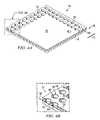
- FIG. 6Ais a graphical representation showing resistance to warpage in a POP assembly of a preferred embodiment of the invention.
- FIG. 6Bis another graphical representation showing resistance to warpage in a POP assembly of a preferred embodiment of the invention.
- a POP assembly 10is shown in the partial cutaway views of FIGS. 1 , 2 and 3 .
- a bottom package 12is affixed to a top package 14 in a configuration to form a completed POP assembly 10 according to a preferred example of the invention.
- each package 12 , 14may include a chip 16 affixed to a substrate 18 having leads or pads 20 for making electrical connections as is known in the arts.
- the terms “bottom” and “top”are used herein to describe the arrangement of the components as shown in the drawings and are not intended to delimit or restrict the spatial relationship of the components in any absolute sense, for example, the POP assembly 10 shown and described could be rotated in any direction or overturned without altering the invention.
- the chip 16is more-or-less centrally located and the leads or contact pads 20 are located at or near the periphery 22 of the substrate 18 surface 24 .
- the chip 16is encapsulated with epoxy, silicone, or alkyd mold compound 26 as known in the arts.
- the encapsulant 26extends to the edge 28 of the substrate 18 , encompassing the area, e.g., the periphery 22 , populated by the contacts 20 .
- the bottom package 12 in this examplehas contact apertures 30 in the encapsulant 26 permitting communication with the contacts 20 at the upper surface 24 of the substrate 18 .
- Contact apertures 30 in the encapsulant 26facilitate the formation of electrical connections with the contacts 20 , preferably using solder balls 32 .
- the top surface 34 of the encapsulant 26provides a uniform rigid structure above the substrate 18 , continuous except for the contact apertures 30 , and adapted for accepting the mounting of another package, for example “top” package 14 , thereon.
- the top package 14is preferably affixed to the bottom package 12 using processes and adhesives familiar in the arts.
- the bottom package 12 and top package 14preferably have corresponding electrical contact pads 20 for forming electrical couplings, e.g., solder balls 32 , for the purpose of enabling the packages 12 , 14 to function in concert. It should be apparent to those skilled in the arts that wirebond connections, or a combination of solder balls and wirebonds, may also be used to make connections between the contacts of the packages.
- a portion of a bottom package 12is shown in close-up cross-section.
- the contact apertures 30provide a path to the contacts 20 at the surface 24 of the substrate 18 at the periphery 22 of the bottom package 12 .
- the encapsulant 26extends to the edge of the substrate 18 forming a package edge 38 of uniform thickness.
- the contact apertures 30are preferably circular in horizontal cross-section (not shown), appearing in FIG. 3 as truncated cone-shaped passageways in the encapsulant 26 .
- the truncated apex 40is more-or-less defined by the area of the contact pad 20 , and the base 42 terminates at the surface of the encapsulant 26 .
- the sidewalls 44 of the contact apertures 30are preferably angled within the range of about 10-30 degrees from vertical, indicated by angle “A” in the Figures.
- angle “A”is not crucial to the practice of the invention, although angles on the order of about 10-30 degrees or greater are presently preferred for present manufacturing processes.
- preferred embodiments of the inventionare also provided with a gas release channel 46 .
- the gas release channel 46provides a path for air and/or other gasses to escape during reflow processes.
- the gas release channelmay be shaped and placed taking into consideration area and/or configuration requirements for the particular application.
- FIGS. 4A through 5BFurther examples of bottom packages 12 according to the invention are shown in FIGS. 4A through 5B .
- FIG. 4Aand corresponding close-up FIG. 4B , show an example of a package with a contact aperture angle A of 10 degrees.
- FIGS. 5A-5Bshow an example with a contact aperture angle A of 30 degrees.
- a larger angle Aas in FIGS. 5A-5B , may be used to accommodate larger solder balls.
- a smaller angle A as shown in the example of FIGS. 4A-4Bmay be used with higher contact pad 20 densities, or may be used to provide increased encapsulant area between contact apertures 30 , providing the package 12 with increased rigidity.
- These examplesare representative of preferred embodiments of the invention.
- There are many possible variations in the configuration of the bottom package 12 , and therefore of the POP assembly 10without departure from the principles of the invention, including sidewalls with longer slopes.
- FIG. 6Ais a graphical representation of an example of a preferred embodiment of a bottom package 12 according to the invention experiencing “sad” (corners downward) flexion forces during testing exposure to room temperature, i.e., 25 degrees C.
- Contour lines 60represent mechanical stress exerted on the package 12 with warpage measured in micrometers. It can be seen that the stresses, and therefore the potential for warpage, tends to be greatest at the corners 62 and edges 64 , in this example, the maximum flexion is about ⁇ 78 um.
- FIG. 6Bshows a graphical representation of a bottom package 12 of the invention subjected to a peak temperature of about 260 degrees C.
Landscapes
- Engineering & Computer Science (AREA)
- Microelectronics & Electronic Packaging (AREA)
- Power Engineering (AREA)
- Physics & Mathematics (AREA)
- Condensed Matter Physics & Semiconductors (AREA)
- General Physics & Mathematics (AREA)
- Computer Hardware Design (AREA)
- Lead Frames For Integrated Circuits (AREA)
- Structures For Mounting Electric Components On Printed Circuit Boards (AREA)
- Structures Or Materials For Encapsulating Or Coating Semiconductor Devices Or Solid State Devices (AREA)
Abstract
Description
Claims (13)
Priority Applications (2)
| Application Number | Priority Date | Filing Date | Title |
|---|---|---|---|
| US11/217,233US7675152B2 (en) | 2005-09-01 | 2005-09-01 | Package-on-package semiconductor assembly |
| PCT/US2006/034043WO2007027902A2 (en) | 2005-09-01 | 2006-08-31 | Package-on-package semiconductor assembly |
Applications Claiming Priority (1)
| Application Number | Priority Date | Filing Date | Title |
|---|---|---|---|
| US11/217,233US7675152B2 (en) | 2005-09-01 | 2005-09-01 | Package-on-package semiconductor assembly |
Publications (2)
| Publication Number | Publication Date |
|---|---|
| US20070052081A1 US20070052081A1 (en) | 2007-03-08 |
| US7675152B2true US7675152B2 (en) | 2010-03-09 |
Family
ID=37809512
Family Applications (1)
| Application Number | Title | Priority Date | Filing Date |
|---|---|---|---|
| US11/217,233Expired - LifetimeUS7675152B2 (en) | 2005-09-01 | 2005-09-01 | Package-on-package semiconductor assembly |
Country Status (2)
| Country | Link |
|---|---|
| US (1) | US7675152B2 (en) |
| WO (1) | WO2007027902A2 (en) |
Cited By (53)
| Publication number | Priority date | Publication date | Assignee | Title |
|---|---|---|---|---|
| US20070148822A1 (en)* | 2005-12-23 | 2007-06-28 | Tessera, Inc. | Microelectronic packages and methods therefor |
| US20100237488A1 (en)* | 2006-01-12 | 2010-09-23 | Hyeog Chan Kwon | Integrated circuit package system including honeycomb molding |
| US20100279504A1 (en)* | 2006-01-12 | 2010-11-04 | Heap Hoe Kuan | Integrated circuit package system including honeycomb molding |
| US20110183465A1 (en)* | 2007-06-22 | 2011-07-28 | Texas Instruments Incorporated | Array-Molded Package-On-Package Having Redistribution Lines |
| US20110233747A1 (en)* | 2010-03-25 | 2011-09-29 | Seongmin Lee | Integrated circuit packaging system with stacking option and method of manufacture thereof |
| US8404520B1 (en) | 2011-10-17 | 2013-03-26 | Invensas Corporation | Package-on-package assembly with wire bond vias |
| US8482111B2 (en) | 2010-07-19 | 2013-07-09 | Tessera, Inc. | Stackable molded microelectronic packages |
| US8525314B2 (en) | 2004-11-03 | 2013-09-03 | Tessera, Inc. | Stacked packaging improvements |
| US8623706B2 (en) | 2010-11-15 | 2014-01-07 | Tessera, Inc. | Microelectronic package with terminals on dielectric mass |
| US8835228B2 (en) | 2012-05-22 | 2014-09-16 | Invensas Corporation | Substrate-less stackable package with wire-bond interconnect |
| US8872318B2 (en) | 2011-08-24 | 2014-10-28 | Tessera, Inc. | Through interposer wire bond using low CTE interposer with coarse slot apertures |
| US8878353B2 (en) | 2012-12-20 | 2014-11-04 | Invensas Corporation | Structure for microelectronic packaging with bond elements to encapsulation surface |
| US8883563B1 (en) | 2013-07-15 | 2014-11-11 | Invensas Corporation | Fabrication of microelectronic assemblies having stack terminals coupled by connectors extending through encapsulation |
| US8975738B2 (en) | 2012-11-12 | 2015-03-10 | Invensas Corporation | Structure for microelectronic packaging with terminals on dielectric mass |
| US9023691B2 (en) | 2013-07-15 | 2015-05-05 | Invensas Corporation | Microelectronic assemblies with stack terminals coupled by connectors extending through encapsulation |
| US9034696B2 (en) | 2013-07-15 | 2015-05-19 | Invensas Corporation | Microelectronic assemblies having reinforcing collars on connectors extending through encapsulation |
| US9082753B2 (en) | 2013-11-12 | 2015-07-14 | Invensas Corporation | Severing bond wire by kinking and twisting |
| US9087815B2 (en) | 2013-11-12 | 2015-07-21 | Invensas Corporation | Off substrate kinking of bond wire |
| US9093435B2 (en) | 2011-05-03 | 2015-07-28 | Tessera, Inc. | Package-on-package assembly with wire bonds to encapsulation surface |
| US9159708B2 (en) | 2010-07-19 | 2015-10-13 | Tessera, Inc. | Stackable molded microelectronic packages with area array unit connectors |
| US9171769B2 (en) | 2010-12-06 | 2015-10-27 | Stats Chippac, Ltd. | Semiconductor device and method of forming openings through encapsulant to reduce warpage and stress on semiconductor package |
| US9214454B2 (en) | 2014-03-31 | 2015-12-15 | Invensas Corporation | Batch process fabrication of package-on-package microelectronic assemblies |
| US9224717B2 (en) | 2011-05-03 | 2015-12-29 | Tessera, Inc. | Package-on-package assembly with wire bonds to encapsulation surface |
| US9324681B2 (en) | 2010-12-13 | 2016-04-26 | Tessera, Inc. | Pin attachment |
| US9349706B2 (en) | 2012-02-24 | 2016-05-24 | Invensas Corporation | Method for package-on-package assembly with wire bonds to encapsulation surface |
| US9391008B2 (en) | 2012-07-31 | 2016-07-12 | Invensas Corporation | Reconstituted wafer-level package DRAM |
| US9412714B2 (en) | 2014-05-30 | 2016-08-09 | Invensas Corporation | Wire bond support structure and microelectronic package including wire bonds therefrom |
| US9502390B2 (en) | 2012-08-03 | 2016-11-22 | Invensas Corporation | BVA interposer |
| US9583411B2 (en) | 2014-01-17 | 2017-02-28 | Invensas Corporation | Fine pitch BVA using reconstituted wafer with area array accessible for testing |
| US9601454B2 (en) | 2013-02-01 | 2017-03-21 | Invensas Corporation | Method of forming a component having wire bonds and a stiffening layer |
| US9646917B2 (en) | 2014-05-29 | 2017-05-09 | Invensas Corporation | Low CTE component with wire bond interconnects |
| US9659848B1 (en) | 2015-11-18 | 2017-05-23 | Invensas Corporation | Stiffened wires for offset BVA |
| US9685365B2 (en) | 2013-08-08 | 2017-06-20 | Invensas Corporation | Method of forming a wire bond having a free end |
| US9691679B2 (en) | 2012-02-24 | 2017-06-27 | Invensas Corporation | Method for package-on-package assembly with wire bonds to encapsulation surface |
| US9728527B2 (en) | 2013-11-22 | 2017-08-08 | Invensas Corporation | Multiple bond via arrays of different wire heights on a same substrate |
| US9735084B2 (en) | 2014-12-11 | 2017-08-15 | Invensas Corporation | Bond via array for thermal conductivity |
| US9761554B2 (en) | 2015-05-07 | 2017-09-12 | Invensas Corporation | Ball bonding metal wire bond wires to metal pads |
| US9812402B2 (en) | 2015-10-12 | 2017-11-07 | Invensas Corporation | Wire bond wires for interference shielding |
| US9842745B2 (en) | 2012-02-17 | 2017-12-12 | Invensas Corporation | Heat spreading substrate with embedded interconnects |
| US9852969B2 (en) | 2013-11-22 | 2017-12-26 | Invensas Corporation | Die stacks with one or more bond via arrays of wire bond wires and with one or more arrays of bump interconnects |
| US9888579B2 (en) | 2015-03-05 | 2018-02-06 | Invensas Corporation | Pressing of wire bond wire tips to provide bent-over tips |
| US9911718B2 (en) | 2015-11-17 | 2018-03-06 | Invensas Corporation | ‘RDL-First’ packaged microelectronic device for a package-on-package device |
| US9935075B2 (en) | 2016-07-29 | 2018-04-03 | Invensas Corporation | Wire bonding method and apparatus for electromagnetic interference shielding |
| US9984992B2 (en) | 2015-12-30 | 2018-05-29 | Invensas Corporation | Embedded wire bond wires for vertical integration with separate surface mount and wire bond mounting surfaces |
| US10008469B2 (en) | 2015-04-30 | 2018-06-26 | Invensas Corporation | Wafer-level packaging using wire bond wires in place of a redistribution layer |
| US10008477B2 (en) | 2013-09-16 | 2018-06-26 | Invensas Corporation | Microelectronic element with bond elements to encapsulation surface |
| US10026717B2 (en) | 2013-11-22 | 2018-07-17 | Invensas Corporation | Multiple bond via arrays of different wire heights on a same substrate |
| US10181457B2 (en) | 2015-10-26 | 2019-01-15 | Invensas Corporation | Microelectronic package for wafer-level chip scale packaging with fan-out |
| US10299368B2 (en) | 2016-12-21 | 2019-05-21 | Invensas Corporation | Surface integrated waveguides and circuit structures therefor |
| US10332854B2 (en) | 2015-10-23 | 2019-06-25 | Invensas Corporation | Anchoring structure of fine pitch bva |
| US10381326B2 (en) | 2014-05-28 | 2019-08-13 | Invensas Corporation | Structure and method for integrated circuits packaging with increased density |
| US10460958B2 (en) | 2013-08-07 | 2019-10-29 | Invensas Corporation | Method of manufacturing embedded packaging with preformed vias |
| US10490528B2 (en) | 2015-10-12 | 2019-11-26 | Invensas Corporation | Embedded wire bond wires |
Families Citing this family (3)
| Publication number | Priority date | Publication date | Assignee | Title |
|---|---|---|---|---|
| US20080258286A1 (en)* | 2007-04-23 | 2008-10-23 | Texas Instruments Incorporated | High Input/Output, Low Profile Package-On-Package Semiconductor System |
| JP2009302505A (en)* | 2008-05-15 | 2009-12-24 | Panasonic Corp | Semiconductor device and method of manufacturing semiconductor device |
| US8716868B2 (en) | 2009-05-20 | 2014-05-06 | Panasonic Corporation | Semiconductor module for stacking and stacked semiconductor module |
Citations (22)
| Publication number | Priority date | Publication date | Assignee | Title |
|---|---|---|---|---|
| US5565709A (en)* | 1994-11-10 | 1996-10-15 | Nitto Denko Corporation | Semiconductor device |
| US5608265A (en)* | 1993-03-17 | 1997-03-04 | Hitachi, Ltd. | Encapsulated semiconductor device package having holes for electrically conductive material |
| US5668405A (en) | 1994-09-14 | 1997-09-16 | Nec Corporation | Semiconductor device with a film carrier tape |
| US5841192A (en)* | 1994-07-21 | 1998-11-24 | Sgs-Thomson Microelectronics S.A. | Injection molded ball grid array casing |
| US5973393A (en) | 1996-12-20 | 1999-10-26 | Lsi Logic Corporation | Apparatus and method for stackable molded lead frame ball grid array packaging of integrated circuits |
| US6130823A (en) | 1999-02-01 | 2000-10-10 | Raytheon E-Systems, Inc. | Stackable ball grid array module and method |
| US6180881B1 (en)* | 1998-05-05 | 2001-01-30 | Harlan Ruben Isaak | Chip stack and method of making same |
| US6250606B1 (en)* | 1999-06-29 | 2001-06-26 | Sharp Kabushiki Kaisha | Substrate for semiconductor device, semiconductor device and manufacturing method thereof |
| US6338813B1 (en) | 1999-10-15 | 2002-01-15 | Advanced Semiconductor Engineering, Inc. | Molding method for BGA semiconductor chip package |
| US20020017710A1 (en) | 2000-08-04 | 2002-02-14 | Seiko Epson Corporation | Semiconductor device and method of manufacturing the same, circuit board, and electronic equipment |
| US6489676B2 (en)* | 2000-12-04 | 2002-12-03 | Fujitsu Limited | Semiconductor device having an interconnecting post formed on an interposer within a sealing resin |
| US6498055B2 (en) | 2000-05-17 | 2002-12-24 | Kabushiki Kaisha Toshiba | Semiconductor device, method of manufacturing semiconductor device, resin molding die, and semiconductor manufacturing system |
| US6503781B2 (en)* | 2000-05-11 | 2003-01-07 | Micron Technology, Inc. | Molded ball grid array |
| US6534338B1 (en) | 2001-06-29 | 2003-03-18 | Amkor Technology, Inc. | Method for molding semiconductor package having a ceramic substrate |
| US20030082848A1 (en)* | 2001-10-25 | 2003-05-01 | Takayuki Ohuchida | Semiconductor device and manufacturing method |
| US20040036164A1 (en)* | 2001-07-31 | 2004-02-26 | Toshihiko Koike | Semiconductor device and its manufacturing method |
| US6767767B2 (en) | 2001-08-31 | 2004-07-27 | Renesas Technology Corp. | Method of manufacturing a semiconductor device in which a block molding package utilizes air vents in a substrate |
| US6774467B2 (en)* | 2000-03-24 | 2004-08-10 | Shinko Electric Industries Co., Ltd | Semiconductor device and process of production of same |
| US6831354B2 (en)* | 2001-08-10 | 2004-12-14 | Oki Electric Industry Co, Ltd. | Semiconductor package and method of fabricating same |
| US20050121764A1 (en)* | 2003-12-04 | 2005-06-09 | Debendra Mallik | Stackable integrated circuit packaging |
| US7094676B1 (en)* | 2000-10-13 | 2006-08-22 | Bridge Semiconductor Corporation | Semiconductor chip assembly with embedded metal pillar |
| US7187068B2 (en)* | 2004-08-11 | 2007-03-06 | Intel Corporation | Methods and apparatuses for providing stacked-die devices |
- 2005
- 2005-09-01USUS11/217,233patent/US7675152B2/ennot_activeExpired - Lifetime
- 2006
- 2006-08-31WOPCT/US2006/034043patent/WO2007027902A2/enactiveApplication Filing
Patent Citations (22)
| Publication number | Priority date | Publication date | Assignee | Title |
|---|---|---|---|---|
| US5608265A (en)* | 1993-03-17 | 1997-03-04 | Hitachi, Ltd. | Encapsulated semiconductor device package having holes for electrically conductive material |
| US5841192A (en)* | 1994-07-21 | 1998-11-24 | Sgs-Thomson Microelectronics S.A. | Injection molded ball grid array casing |
| US5668405A (en) | 1994-09-14 | 1997-09-16 | Nec Corporation | Semiconductor device with a film carrier tape |
| US5565709A (en)* | 1994-11-10 | 1996-10-15 | Nitto Denko Corporation | Semiconductor device |
| US5973393A (en) | 1996-12-20 | 1999-10-26 | Lsi Logic Corporation | Apparatus and method for stackable molded lead frame ball grid array packaging of integrated circuits |
| US6180881B1 (en)* | 1998-05-05 | 2001-01-30 | Harlan Ruben Isaak | Chip stack and method of making same |
| US6130823A (en) | 1999-02-01 | 2000-10-10 | Raytheon E-Systems, Inc. | Stackable ball grid array module and method |
| US6250606B1 (en)* | 1999-06-29 | 2001-06-26 | Sharp Kabushiki Kaisha | Substrate for semiconductor device, semiconductor device and manufacturing method thereof |
| US6338813B1 (en) | 1999-10-15 | 2002-01-15 | Advanced Semiconductor Engineering, Inc. | Molding method for BGA semiconductor chip package |
| US6774467B2 (en)* | 2000-03-24 | 2004-08-10 | Shinko Electric Industries Co., Ltd | Semiconductor device and process of production of same |
| US6503781B2 (en)* | 2000-05-11 | 2003-01-07 | Micron Technology, Inc. | Molded ball grid array |
| US6498055B2 (en) | 2000-05-17 | 2002-12-24 | Kabushiki Kaisha Toshiba | Semiconductor device, method of manufacturing semiconductor device, resin molding die, and semiconductor manufacturing system |
| US20020017710A1 (en) | 2000-08-04 | 2002-02-14 | Seiko Epson Corporation | Semiconductor device and method of manufacturing the same, circuit board, and electronic equipment |
| US7094676B1 (en)* | 2000-10-13 | 2006-08-22 | Bridge Semiconductor Corporation | Semiconductor chip assembly with embedded metal pillar |
| US6489676B2 (en)* | 2000-12-04 | 2002-12-03 | Fujitsu Limited | Semiconductor device having an interconnecting post formed on an interposer within a sealing resin |
| US6534338B1 (en) | 2001-06-29 | 2003-03-18 | Amkor Technology, Inc. | Method for molding semiconductor package having a ceramic substrate |
| US20040036164A1 (en)* | 2001-07-31 | 2004-02-26 | Toshihiko Koike | Semiconductor device and its manufacturing method |
| US6831354B2 (en)* | 2001-08-10 | 2004-12-14 | Oki Electric Industry Co, Ltd. | Semiconductor package and method of fabricating same |
| US6767767B2 (en) | 2001-08-31 | 2004-07-27 | Renesas Technology Corp. | Method of manufacturing a semiconductor device in which a block molding package utilizes air vents in a substrate |
| US20030082848A1 (en)* | 2001-10-25 | 2003-05-01 | Takayuki Ohuchida | Semiconductor device and manufacturing method |
| US20050121764A1 (en)* | 2003-12-04 | 2005-06-09 | Debendra Mallik | Stackable integrated circuit packaging |
| US7187068B2 (en)* | 2004-08-11 | 2007-03-06 | Intel Corporation | Methods and apparatuses for providing stacked-die devices |
Cited By (115)
| Publication number | Priority date | Publication date | Assignee | Title |
|---|---|---|---|---|
| US8531020B2 (en) | 2004-11-03 | 2013-09-10 | Tessera, Inc. | Stacked packaging improvements |
| US9153562B2 (en) | 2004-11-03 | 2015-10-06 | Tessera, Inc. | Stacked packaging improvements |
| US8525314B2 (en) | 2004-11-03 | 2013-09-03 | Tessera, Inc. | Stacked packaging improvements |
| US8927337B2 (en) | 2004-11-03 | 2015-01-06 | Tessera, Inc. | Stacked packaging improvements |
| US9570416B2 (en) | 2004-11-03 | 2017-02-14 | Tessera, Inc. | Stacked packaging improvements |
| US8728865B2 (en) | 2005-12-23 | 2014-05-20 | Tessera, Inc. | Microelectronic packages and methods therefor |
| US20100232129A1 (en)* | 2005-12-23 | 2010-09-16 | Tessera, Inc. | Microelectronic packages and methods therefor |
| US9984901B2 (en) | 2005-12-23 | 2018-05-29 | Tessera, Inc. | Method for making a microelectronic assembly having conductive elements |
| US20070148822A1 (en)* | 2005-12-23 | 2007-06-28 | Tessera, Inc. | Microelectronic packages and methods therefor |
| US8058101B2 (en) | 2005-12-23 | 2011-11-15 | Tessera, Inc. | Microelectronic packages and methods therefor |
| US8093697B2 (en) | 2005-12-23 | 2012-01-10 | Tessera, Inc. | Microelectronic packages and methods therefor |
| US9218988B2 (en) | 2005-12-23 | 2015-12-22 | Tessera, Inc. | Microelectronic packages and methods therefor |
| US8409921B2 (en)* | 2006-01-12 | 2013-04-02 | Stats Chippac Ltd. | Integrated circuit package system including honeycomb molding |
| US8217501B2 (en)* | 2006-01-12 | 2012-07-10 | Stats Chippac Ltd. | Integrated circuit package system including honeycomb molding |
| US20100279504A1 (en)* | 2006-01-12 | 2010-11-04 | Heap Hoe Kuan | Integrated circuit package system including honeycomb molding |
| US20100237488A1 (en)* | 2006-01-12 | 2010-09-23 | Hyeog Chan Kwon | Integrated circuit package system including honeycomb molding |
| US8304285B2 (en) | 2007-06-22 | 2012-11-06 | Texas Instruments Incorporated | Array-molded package-on-package having redistribution lines |
| US20110183465A1 (en)* | 2007-06-22 | 2011-07-28 | Texas Instruments Incorporated | Array-Molded Package-On-Package Having Redistribution Lines |
| US8378476B2 (en) | 2010-03-25 | 2013-02-19 | Stats Chippac Ltd. | Integrated circuit packaging system with stacking option and method of manufacture thereof |
| US20110233747A1 (en)* | 2010-03-25 | 2011-09-29 | Seongmin Lee | Integrated circuit packaging system with stacking option and method of manufacture thereof |
| US8907466B2 (en) | 2010-07-19 | 2014-12-09 | Tessera, Inc. | Stackable molded microelectronic packages |
| US9159708B2 (en) | 2010-07-19 | 2015-10-13 | Tessera, Inc. | Stackable molded microelectronic packages with area array unit connectors |
| US10128216B2 (en) | 2010-07-19 | 2018-11-13 | Tessera, Inc. | Stackable molded microelectronic packages |
| US8482111B2 (en) | 2010-07-19 | 2013-07-09 | Tessera, Inc. | Stackable molded microelectronic packages |
| US9123664B2 (en) | 2010-07-19 | 2015-09-01 | Tessera, Inc. | Stackable molded microelectronic packages |
| US9570382B2 (en) | 2010-07-19 | 2017-02-14 | Tessera, Inc. | Stackable molded microelectronic packages |
| US9553076B2 (en) | 2010-07-19 | 2017-01-24 | Tessera, Inc. | Stackable molded microelectronic packages with area array unit connectors |
| US8637991B2 (en) | 2010-11-15 | 2014-01-28 | Tessera, Inc. | Microelectronic package with terminals on dielectric mass |
| US8623706B2 (en) | 2010-11-15 | 2014-01-07 | Tessera, Inc. | Microelectronic package with terminals on dielectric mass |
| US8957527B2 (en) | 2010-11-15 | 2015-02-17 | Tessera, Inc. | Microelectronic package with terminals on dielectric mass |
| US8659164B2 (en) | 2010-11-15 | 2014-02-25 | Tessera, Inc. | Microelectronic package with terminals on dielectric mass |
| US9171769B2 (en) | 2010-12-06 | 2015-10-27 | Stats Chippac, Ltd. | Semiconductor device and method of forming openings through encapsulant to reduce warpage and stress on semiconductor package |
| US9324681B2 (en) | 2010-12-13 | 2016-04-26 | Tessera, Inc. | Pin attachment |
| US11424211B2 (en) | 2011-05-03 | 2022-08-23 | Tessera Llc | Package-on-package assembly with wire bonds to encapsulation surface |
| US9224717B2 (en) | 2011-05-03 | 2015-12-29 | Tessera, Inc. | Package-on-package assembly with wire bonds to encapsulation surface |
| US9093435B2 (en) | 2011-05-03 | 2015-07-28 | Tessera, Inc. | Package-on-package assembly with wire bonds to encapsulation surface |
| US10593643B2 (en) | 2011-05-03 | 2020-03-17 | Tessera, Inc. | Package-on-package assembly with wire bonds to encapsulation surface |
| US9691731B2 (en) | 2011-05-03 | 2017-06-27 | Tessera, Inc. | Package-on-package assembly with wire bonds to encapsulation surface |
| US10062661B2 (en) | 2011-05-03 | 2018-08-28 | Tessera, Inc. | Package-on-package assembly with wire bonds to encapsulation surface |
| US8872318B2 (en) | 2011-08-24 | 2014-10-28 | Tessera, Inc. | Through interposer wire bond using low CTE interposer with coarse slot apertures |
| US9041227B2 (en) | 2011-10-17 | 2015-05-26 | Invensas Corporation | Package-on-package assembly with wire bond vias |
| US9761558B2 (en) | 2011-10-17 | 2017-09-12 | Invensas Corporation | Package-on-package assembly with wire bond vias |
| US9105483B2 (en) | 2011-10-17 | 2015-08-11 | Invensas Corporation | Package-on-package assembly with wire bond vias |
| US9252122B2 (en) | 2011-10-17 | 2016-02-02 | Invensas Corporation | Package-on-package assembly with wire bond vias |
| US10756049B2 (en) | 2011-10-17 | 2020-08-25 | Invensas Corporation | Package-on-package assembly with wire bond vias |
| US8404520B1 (en) | 2011-10-17 | 2013-03-26 | Invensas Corporation | Package-on-package assembly with wire bond vias |
| US8836136B2 (en) | 2011-10-17 | 2014-09-16 | Invensas Corporation | Package-on-package assembly with wire bond vias |
| US11735563B2 (en) | 2011-10-17 | 2023-08-22 | Invensas Llc | Package-on-package assembly with wire bond vias |
| US11189595B2 (en) | 2011-10-17 | 2021-11-30 | Invensas Corporation | Package-on-package assembly with wire bond vias |
| US9842745B2 (en) | 2012-02-17 | 2017-12-12 | Invensas Corporation | Heat spreading substrate with embedded interconnects |
| US9349706B2 (en) | 2012-02-24 | 2016-05-24 | Invensas Corporation | Method for package-on-package assembly with wire bonds to encapsulation surface |
| US9691679B2 (en) | 2012-02-24 | 2017-06-27 | Invensas Corporation | Method for package-on-package assembly with wire bonds to encapsulation surface |
| US8835228B2 (en) | 2012-05-22 | 2014-09-16 | Invensas Corporation | Substrate-less stackable package with wire-bond interconnect |
| US10170412B2 (en) | 2012-05-22 | 2019-01-01 | Invensas Corporation | Substrate-less stackable package with wire-bond interconnect |
| US10510659B2 (en) | 2012-05-22 | 2019-12-17 | Invensas Corporation | Substrate-less stackable package with wire-bond interconnect |
| US9953914B2 (en) | 2012-05-22 | 2018-04-24 | Invensas Corporation | Substrate-less stackable package with wire-bond interconnect |
| US9917073B2 (en) | 2012-07-31 | 2018-03-13 | Invensas Corporation | Reconstituted wafer-level package dram with conductive interconnects formed in encapsulant at periphery of the package |
| US9391008B2 (en) | 2012-07-31 | 2016-07-12 | Invensas Corporation | Reconstituted wafer-level package DRAM |
| US10297582B2 (en) | 2012-08-03 | 2019-05-21 | Invensas Corporation | BVA interposer |
| US9502390B2 (en) | 2012-08-03 | 2016-11-22 | Invensas Corporation | BVA interposer |
| US8975738B2 (en) | 2012-11-12 | 2015-03-10 | Invensas Corporation | Structure for microelectronic packaging with terminals on dielectric mass |
| US9615456B2 (en) | 2012-12-20 | 2017-04-04 | Invensas Corporation | Microelectronic assembly for microelectronic packaging with bond elements to encapsulation surface |
| US8878353B2 (en) | 2012-12-20 | 2014-11-04 | Invensas Corporation | Structure for microelectronic packaging with bond elements to encapsulation surface |
| US9095074B2 (en) | 2012-12-20 | 2015-07-28 | Invensas Corporation | Structure for microelectronic packaging with bond elements to encapsulation surface |
| US9601454B2 (en) | 2013-02-01 | 2017-03-21 | Invensas Corporation | Method of forming a component having wire bonds and a stiffening layer |
| US9633979B2 (en) | 2013-07-15 | 2017-04-25 | Invensas Corporation | Microelectronic assemblies having stack terminals coupled by connectors extending through encapsulation |
| US8883563B1 (en) | 2013-07-15 | 2014-11-11 | Invensas Corporation | Fabrication of microelectronic assemblies having stack terminals coupled by connectors extending through encapsulation |
| US9034696B2 (en) | 2013-07-15 | 2015-05-19 | Invensas Corporation | Microelectronic assemblies having reinforcing collars on connectors extending through encapsulation |
| US9023691B2 (en) | 2013-07-15 | 2015-05-05 | Invensas Corporation | Microelectronic assemblies with stack terminals coupled by connectors extending through encapsulation |
| US10460958B2 (en) | 2013-08-07 | 2019-10-29 | Invensas Corporation | Method of manufacturing embedded packaging with preformed vias |
| US9685365B2 (en) | 2013-08-08 | 2017-06-20 | Invensas Corporation | Method of forming a wire bond having a free end |
| US10008477B2 (en) | 2013-09-16 | 2018-06-26 | Invensas Corporation | Microelectronic element with bond elements to encapsulation surface |
| US9893033B2 (en) | 2013-11-12 | 2018-02-13 | Invensas Corporation | Off substrate kinking of bond wire |
| US9087815B2 (en) | 2013-11-12 | 2015-07-21 | Invensas Corporation | Off substrate kinking of bond wire |
| US9082753B2 (en) | 2013-11-12 | 2015-07-14 | Invensas Corporation | Severing bond wire by kinking and twisting |
| US9852969B2 (en) | 2013-11-22 | 2017-12-26 | Invensas Corporation | Die stacks with one or more bond via arrays of wire bond wires and with one or more arrays of bump interconnects |
| US9728527B2 (en) | 2013-11-22 | 2017-08-08 | Invensas Corporation | Multiple bond via arrays of different wire heights on a same substrate |
| US10629567B2 (en) | 2013-11-22 | 2020-04-21 | Invensas Corporation | Multiple plated via arrays of different wire heights on same substrate |
| USRE49987E1 (en) | 2013-11-22 | 2024-05-28 | Invensas Llc | Multiple plated via arrays of different wire heights on a same substrate |
| US10290613B2 (en) | 2013-11-22 | 2019-05-14 | Invensas Corporation | Multiple bond via arrays of different wire heights on a same substrate |
| US10026717B2 (en) | 2013-11-22 | 2018-07-17 | Invensas Corporation | Multiple bond via arrays of different wire heights on a same substrate |
| US9583411B2 (en) | 2014-01-17 | 2017-02-28 | Invensas Corporation | Fine pitch BVA using reconstituted wafer with area array accessible for testing |
| US9837330B2 (en) | 2014-01-17 | 2017-12-05 | Invensas Corporation | Fine pitch BVA using reconstituted wafer with area array accessible for testing |
| US10529636B2 (en) | 2014-01-17 | 2020-01-07 | Invensas Corporation | Fine pitch BVA using reconstituted wafer with area array accessible for testing |
| US11404338B2 (en) | 2014-01-17 | 2022-08-02 | Invensas Corporation | Fine pitch bva using reconstituted wafer with area array accessible for testing |
| US11990382B2 (en) | 2014-01-17 | 2024-05-21 | Adeia Semiconductor Technologies Llc | Fine pitch BVA using reconstituted wafer with area array accessible for testing |
| US9214454B2 (en) | 2014-03-31 | 2015-12-15 | Invensas Corporation | Batch process fabrication of package-on-package microelectronic assemblies |
| US9812433B2 (en) | 2014-03-31 | 2017-11-07 | Invensas Corporation | Batch process fabrication of package-on-package microelectronic assemblies |
| US9356006B2 (en) | 2014-03-31 | 2016-05-31 | Invensas Corporation | Batch process fabrication of package-on-package microelectronic assemblies |
| US10381326B2 (en) | 2014-05-28 | 2019-08-13 | Invensas Corporation | Structure and method for integrated circuits packaging with increased density |
| US9646917B2 (en) | 2014-05-29 | 2017-05-09 | Invensas Corporation | Low CTE component with wire bond interconnects |
| US10032647B2 (en) | 2014-05-29 | 2018-07-24 | Invensas Corporation | Low CTE component with wire bond interconnects |
| US10475726B2 (en) | 2014-05-29 | 2019-11-12 | Invensas Corporation | Low CTE component with wire bond interconnects |
| US9412714B2 (en) | 2014-05-30 | 2016-08-09 | Invensas Corporation | Wire bond support structure and microelectronic package including wire bonds therefrom |
| US9947641B2 (en) | 2014-05-30 | 2018-04-17 | Invensas Corporation | Wire bond support structure and microelectronic package including wire bonds therefrom |
| US9735084B2 (en) | 2014-12-11 | 2017-08-15 | Invensas Corporation | Bond via array for thermal conductivity |
| US10806036B2 (en) | 2015-03-05 | 2020-10-13 | Invensas Corporation | Pressing of wire bond wire tips to provide bent-over tips |
| US9888579B2 (en) | 2015-03-05 | 2018-02-06 | Invensas Corporation | Pressing of wire bond wire tips to provide bent-over tips |
| US10008469B2 (en) | 2015-04-30 | 2018-06-26 | Invensas Corporation | Wafer-level packaging using wire bond wires in place of a redistribution layer |
| US9761554B2 (en) | 2015-05-07 | 2017-09-12 | Invensas Corporation | Ball bonding metal wire bond wires to metal pads |
| US10559537B2 (en) | 2015-10-12 | 2020-02-11 | Invensas Corporation | Wire bond wires for interference shielding |
| US10115678B2 (en) | 2015-10-12 | 2018-10-30 | Invensas Corporation | Wire bond wires for interference shielding |
| US9812402B2 (en) | 2015-10-12 | 2017-11-07 | Invensas Corporation | Wire bond wires for interference shielding |
| US10490528B2 (en) | 2015-10-12 | 2019-11-26 | Invensas Corporation | Embedded wire bond wires |
| US11462483B2 (en) | 2015-10-12 | 2022-10-04 | Invensas Llc | Wire bond wires for interference shielding |
| US10332854B2 (en) | 2015-10-23 | 2019-06-25 | Invensas Corporation | Anchoring structure of fine pitch bva |
| US10181457B2 (en) | 2015-10-26 | 2019-01-15 | Invensas Corporation | Microelectronic package for wafer-level chip scale packaging with fan-out |
| US10043779B2 (en) | 2015-11-17 | 2018-08-07 | Invensas Corporation | Packaged microelectronic device for a package-on-package device |
| US9911718B2 (en) | 2015-11-17 | 2018-03-06 | Invensas Corporation | ‘RDL-First’ packaged microelectronic device for a package-on-package device |
| US9659848B1 (en) | 2015-11-18 | 2017-05-23 | Invensas Corporation | Stiffened wires for offset BVA |
| US9984992B2 (en) | 2015-12-30 | 2018-05-29 | Invensas Corporation | Embedded wire bond wires for vertical integration with separate surface mount and wire bond mounting surfaces |
| US10325877B2 (en) | 2015-12-30 | 2019-06-18 | Invensas Corporation | Embedded wire bond wires for vertical integration with separate surface mount and wire bond mounting surfaces |
| US9935075B2 (en) | 2016-07-29 | 2018-04-03 | Invensas Corporation | Wire bonding method and apparatus for electromagnetic interference shielding |
| US10658302B2 (en) | 2016-07-29 | 2020-05-19 | Invensas Corporation | Wire bonding method and apparatus for electromagnetic interference shielding |
| US10299368B2 (en) | 2016-12-21 | 2019-05-21 | Invensas Corporation | Surface integrated waveguides and circuit structures therefor |
Also Published As
| Publication number | Publication date |
|---|---|
| WO2007027902A2 (en) | 2007-03-08 |
| WO2007027902A3 (en) | 2007-05-31 |
| US20070052081A1 (en) | 2007-03-08 |
Similar Documents
| Publication | Publication Date | Title |
|---|---|---|
| US7675152B2 (en) | Package-on-package semiconductor assembly | |
| US6770961B2 (en) | Carrier frame and semiconductor package including carrier frame | |
| USRE45463E1 (en) | Stacked microelectronic assemblies with central contacts | |
| US7050303B2 (en) | Semiconductor module with vertically mounted semiconductor chip packages | |
| US6657296B2 (en) | Semicondctor package | |
| US7317247B2 (en) | Semiconductor package having heat spreader and package stack using the same | |
| JP3685947B2 (en) | Semiconductor device and manufacturing method thereof | |
| US7327020B2 (en) | Multi-chip package including at least one semiconductor device enclosed therein | |
| JP5522561B2 (en) | Microelectronic device package, stacked microelectronic device package, and method of manufacturing microelectronic device | |
| KR101070913B1 (en) | Stacked die package | |
| US6856013B1 (en) | Integrated circuit packages, ball-grid array integrated circuit packages and methods of packaging an integrated circuit | |
| US6841858B2 (en) | Leadframe for die stacking applications and related die stacking concepts | |
| US20090032913A1 (en) | Component and assemblies with ends offset downwardly | |
| US12205866B2 (en) | Semiconductor device | |
| KR100674907B1 (en) | Highly reliable stackable semiconductor package | |
| US20060226543A1 (en) | Ball grid array package stack | |
| KR20090043945A (en) | Stack package | |
| US20120074549A1 (en) | Semiconductor device with exposed pad | |
| US20080042277A1 (en) | BGA package with leads on chip field of the invention | |
| US8519522B2 (en) | Semiconductor package | |
| US6169322B1 (en) | Die attach pad adapted to reduce delamination stress and method of using same | |
| US20040061222A1 (en) | Window-type ball grid array semiconductor package | |
| JPH11289031A (en) | Semiconductor device and manufacturing method thereof | |
| KR100570512B1 (en) | Chip Scale Semiconductor Package | |
| US20030064542A1 (en) | Methods of packaging an integrated circuit |
Legal Events
| Date | Code | Title | Description |
|---|---|---|---|
| AS | Assignment | Owner name:TEXAS INSTRUMENTS INCORPORATED, TEXAS Free format text:ASSIGNMENT OF ASSIGNORS INTEREST;ASSIGNORS:GERBER, MARK ALLEN;O'CONNER, SHAWN MARTIN;REEL/FRAME:016951/0478;SIGNING DATES FROM 20050816 TO 20050901 Owner name:TEXAS INSTRUMENTS INCORPORATED,TEXAS Free format text:ASSIGNMENT OF ASSIGNORS INTEREST;ASSIGNORS:GERBER, MARK ALLEN;O'CONNER, SHAWN MARTIN;SIGNING DATES FROM 20050816 TO 20050901;REEL/FRAME:016951/0478 | |
| STCF | Information on status: patent grant | Free format text:PATENTED CASE | |
| FPAY | Fee payment | Year of fee payment:4 | |
| MAFP | Maintenance fee payment | Free format text:PAYMENT OF MAINTENANCE FEE, 8TH YEAR, LARGE ENTITY (ORIGINAL EVENT CODE: M1552) Year of fee payment:8 | |
| MAFP | Maintenance fee payment | Free format text:PAYMENT OF MAINTENANCE FEE, 12TH YEAR, LARGE ENTITY (ORIGINAL EVENT CODE: M1553); ENTITY STATUS OF PATENT OWNER: LARGE ENTITY Year of fee payment:12 |