US7675021B2 - Two dimensional contact image sensor with frontlighting - Google Patents
Two dimensional contact image sensor with frontlightingDownload PDFInfo
- Publication number
- US7675021B2 US7675021B2US12/178,636US17863608AUS7675021B2US 7675021 B2US7675021 B2US 7675021B2US 17863608 AUS17863608 AUS 17863608AUS 7675021 B2US7675021 B2US 7675021B2
- Authority
- US
- United States
- Prior art keywords
- photodetectors
- light
- image sensor
- array
- emitters
- Prior art date
- Legal status (The legal status is an assumption and is not a legal conclusion. Google has not performed a legal analysis and makes no representation as to the accuracy of the status listed.)
- Expired - Fee Related
Links
Images


Classifications
- H—ELECTRICITY
- H10—SEMICONDUCTOR DEVICES; ELECTRIC SOLID-STATE DEVICES NOT OTHERWISE PROVIDED FOR
- H10F—INORGANIC SEMICONDUCTOR DEVICES SENSITIVE TO INFRARED RADIATION, LIGHT, ELECTROMAGNETIC RADIATION OF SHORTER WAVELENGTH OR CORPUSCULAR RADIATION
- H10F39/00—Integrated devices, or assemblies of multiple devices, comprising at least one element covered by group H10F30/00, e.g. radiation detectors comprising photodiode arrays
- H10F39/10—Integrated devices
- H10F39/12—Image sensors
- H10F39/198—Contact-type image sensors [CIS]
- G—PHYSICS
- G06—COMPUTING OR CALCULATING; COUNTING
- G06V—IMAGE OR VIDEO RECOGNITION OR UNDERSTANDING
- G06V40/00—Recognition of biometric, human-related or animal-related patterns in image or video data
- G06V40/10—Human or animal bodies, e.g. vehicle occupants or pedestrians; Body parts, e.g. hands
- G06V40/12—Fingerprints or palmprints
- G06V40/13—Sensors therefor
- G06V40/1318—Sensors therefor using electro-optical elements or layers, e.g. electroluminescent sensing
- H—ELECTRICITY
- H10—SEMICONDUCTOR DEVICES; ELECTRIC SOLID-STATE DEVICES NOT OTHERWISE PROVIDED FOR
- H10F—INORGANIC SEMICONDUCTOR DEVICES SENSITIVE TO INFRARED RADIATION, LIGHT, ELECTROMAGNETIC RADIATION OF SHORTER WAVELENGTH OR CORPUSCULAR RADIATION
- H10F39/00—Integrated devices, or assemblies of multiple devices, comprising at least one element covered by group H10F30/00, e.g. radiation detectors comprising photodiode arrays
- H10F39/80—Constructional details of image sensors
- H10F39/805—Coatings
- H10F39/8057—Optical shielding
Definitions
- the present inventionrelates generally to image sensors and, in particular, to a self-illuminating image sensor being able to be in contacting with a surface to be scanned.
- Prior art image sensors that are close to, or in contact with the surfaceare typically one-dimensional.
- the reason for using a one-dimensional photodetector array in such image sensorsis to allow the surface to be illuminated from a light source parallel to the photodetector array.
- the surface and the photodetector arrayare moved relative to each other.
- the surfaceis coded using densely spaced dot patterns.
- the dots patternstypically encode at least a position on the surface.
- One such a patternuses dots spaced 120 microns apart. In order to achieve a minimum sampling rate of two, an image sensor is needed with a photodetector size of 60 microns, or minimum resolution of 423 pixels per inch (ppi).
- the dot patternsare two-dimensional patterns, and in one specific case each pattern has an extent of 100 pixels by 100 pixels.
- the image sensorAs the two-dimensional extent of the image sensor increases to match that of the pattern to be sensed, providing illumination for the surface becomes increasingly difficult.
- the image sensortypically blocks light from reaching the surface underneath the centre regions of the sensor.
- a typical solutionis to space the sensor away from the surface, but such a solution introduces further problems with regards to focussing the sensor.
- an image sensorcomprising:
- channels etched through said silicon substratefor allowing light to pass through said substrate to a surface
- said array of photodetectorsis arranged to detect reflections of light from said surface.
- an image sensorcomprising:
- a light sourcearranged on a first side of said array of photodetectors for emitting light through said array of photodetectors and at least onto a surface on a second side of said array of photodetectors
- said array of photodetectorsis arranged to detect reflections of light from said surface.
- an image sensorcomprising:
- one or more emittersdirected towards said first side of said array of photodetectors, said one or more emitters emitting light of a first wavelength when illuminated by light of a second wavelength;
- a light sourcefor illuminating said one or more emitters, said light source emitting light of said second wavelength
- a filterfor preventing light of said second wavelength from illuminating said photodetectors.
- the image sensorfurther comprising a spacer for spacing said array of photodetectors from said surface.
- the image sensorfurther comprising a diffuser on a first side of said array of photodetectors, wherein a light source is associated with said diffuser to light said diffuser internally, and light leaking from said diffuser passes through said substrate to said surface.
- said channelshave reflective side walls.
- the image sensorfurther comprising an aperture and lens associated with each photodetector for controlling a field of view of each photodetector.
- said spaceris an at least partially opaque planar layer between said array of photodetectors and said surface, said at least partially opaque planar layer having first pathways corresponding to said channels for allowing light that passed through said channels to pass to said surface, and second pathways corresponding to said photodetectors for allowing light to pass from said surface to said photodetectors.
- the image sensorfurther comprising a reflective layer associated with said diffuser for directing light towards said array of photodetectors.
- an image sensorcomprising:
- a light sourcearranged on a first side of said array of photodetectors for emitting light through said array of photodetectors and at least onto a surface on a second side of said array of photodetectors
- said array of photodetectorsis arranged to detect reflections of light from said surface.
- the image sensorfurther comprising a spacer arranged on the second side of said array of photodetectors for spacing said array of photodetectors from said surface.
- the image sensorfurther comprising a diffuser on said first side of said array of photodetectors, wherein said light source is associated with said diffuser to light said diffuser internally, and light leaking from said diffuser passes through said array of photodetectors.
- the image sensorfurther comprising opaque covers for preventing light emitted from said diffuser from illuminating said array of photodetectors.
- said array of photodetectorsis manufactured from a silicon wafer and a bulk of said silicon wafer forms said opaque covers.
- said array of photodetectorsis manufactured from a silicon wafer and a bulk of said silicon wafer comprises etched channels allowing light to pass from said first side of said array of photodetectors.
- said channelshave reflective side walls.
- the image sensorfurther comprising an aperture and lens associated with each photodetector for controlling a field of view of each photodetector.
- the image sensorfurther comprising a spacer arranged on the second side of said array of photodetector for spacing said array of photodetectors from said surface, said spacer being an at least partially opaque planar layer having first pathways corresponding to said channels for allowing light to pass from said first side to said surface, and second pathways corresponding to said photodetectors for allowing light to pass from said surface to said photodetectors.
- the image sensorfurther comprising a reflective layer associated with said diffuser for directing light towards said array of photodetectors.
- the image sensorfurther comprising:
- said one or more emittersare interleaved with said photodetectors.
- said filteris arranged in a layer between said array of photodetectors and said one or more emitters.
- the image sensorfurther comprising a second filter for preventing light of said second wavelength from illuminating a surface on said first side of said array of photodetectors,
- said array of photodetectorsis arranged to detect reflections of light from said surface.
- the image sensorfurther comprising a transparent layer between said filters for directing light from said light source to said one or more emitters.
- said transparent layeracts as a spacer for spacing said array of photodetectors from said surface.
- the image sensorfurther comprising opaque covers for preventing light emitted from said one or more emitters from illuminating said array of photodetectors.
- said one or more emittersare printed on said filter and directed towards said first side of said array of photodetectors.
- light of said first wavelengthis Infrared light
- light of said second wavelengthis Ultraviolet light
- FIG. 1shows a cross-sectional view of a two-dimensional image sensor having a back light
- FIG. 2shows a cross-sectional view of a two-dimensional image sensor having a back light where the array of photodetectors is fabricated in a silicon wafer;
- FIG. 3shows a plan view of the silicon wafer of the two-dimensional image sensor shown in FIG. 2 ;
- FIG. 4shows a cross-sectional view of a two-dimensional image sensor having a front light
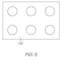
- FIG. 5shows a plan view of the image sensor 200 shown in FIG. 4 .
- FIG. 1shows a cross-sectional view of a two-dimensional image sensor 100 having a back light.
- the image sensor 100includes an array of photodetectors 120 , also known as photodiodes or pixel sensors, with each photodetector 120 providing a signal based upon an amount of illumination sensed by the photodetector 120 .
- the image sensor 100 shownincludes only 2 columns of photodetectors 120 , but those skilled in the present art would understand that the number of photodetectors 120 included in the image sensor 100 is determined by its application.
- the image sensor 100is further provided with a spacer 150 arranged underneath the array of photodetectors 120 for spacing the photodetectors 120 from an underlying surface 110 .
- the spacer 150is a transparent layer.
- the backlight of the image sensor 100is provided by a diffusively transmissive medium 130 attached above the array of photodetectors 120 .
- the diffusively transmissive medium 130is lit by one or more Light Emitting Diodes (LEDs) 135 arranged along one or more edges of the diffusively transmissive medium 130 .
- the light emitted by the LEDs 135reflects within the transmissive medium 130 , carrying the light throughout the transmissive medium 130 . Some of the light leaks out along the planar surfaces of the diffusively transmissive medium 130 .
- the diffusively transmissive medium 130is provided with a reflective layer 140 on the upper planar surface of the diffusively transmissive medium 130 .
- the reflective layer 140reflects light back towards the array of photodetectors 120 and the underlying surface 110 .
- Each photodetector 120is also provided with a cap 125 for shielding the photodetector 120 from being illuminated with light emitted directly from the diffusively transmissive medium 130 . In this manner, the photodetectors 120 are only responsive to light reflected by the underlying surface 110 .
- FIG. 2shows a cross-sectional view of a two-dimensional image sensor 101 having a backlight where the array of photodetectors 120 is fabricated in a silicon wafer.
- the bulk 190 of the silicon waferacts as the caps 125 ( FIG. 1 ), shielding the photodetector 120 from being illuminated directly from the diffusively transmissive medium 130 .
- FIG. 3shows a plan view of the silicon wafer of the two-dimensional image sensor 101 shown in FIG. 2 .
- channels 180are etched through the silicon wafer to allow light to pass from the diffusively transmissive medium 130 towards the underlying surface 110 .
- the sidewalls of the etched channels 180are made reflective, allow the channels to partially act as light pipes.
- light escaping from the diffusively transmissive medium 130passes past the photodetectors 120 , passes through the transparent layer 150 , and onto the underlying surface 110 .
- the underlying surface 110has light absorbing regions 111 and light reflective regions 112 .
- the light absorbing regions 111absorb light, whereas the light reflective regions 112 reflect light illuminating that region.
- one or more photodetectors 120 located above light reflective regions 112senses the illumination, and provide a corresponding signal.
- each photodetector 120is provided with an aperture and a lens.
- the aperture and lensrestricts the field of view of the photodetectors 120 , thereby minimising blurring of the “image” captured by the image sensor.
- blurringis minimised by decreasing the area of the photodetectors 120 , and surrounding each photodetector 120 by a further photodetector, for example in a concentric cylindrical fashion.
- the further photodetectorssense scattered photons, and the output signal of photodetector 120 is altered based upon the signal output by the further photodetector associated with the photodetector 120 .
- blurringis minimised by using a layer of silicon is spacer 150 .
- the layer of siliconhas both illumination and photodetector light channels etched through it. Referring to FIG. 2 , channels or pathways corresponding to the channels 180 are provided for allowing light to pass from the diffusively transmissive medium 130 to the underlying surface 110 , as well as channels or pathways corresponding to the photodetectors 120 for allowing light to pass from the underlying surface 110 to said photodetectors 120 .
- the emission layer(s) and transparent anode of a large-area IR OLEDcan be deposited onto the surface of the entire image sensor, using a metal mask as the cathode.
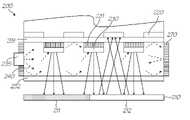
- FIG. 4shows a cross-sectional view of a two-dimensional image sensor 200 having a front light.
- Image sensor 200also includes an array of photodetectors 220 for providing signals based upon an amount of illumination received by respective photodetectors 220 .
- the front light of the image sensor 200is provided by Ultraviolet-stimulated (UV-stimulated) fluorescent (or phosphorescent) Infrared (IR) emitter 230 .
- Emitter 230operates by releasing IR illumination when the emitter 230 is illuminated with UV light.
- FIG. 5shows a plan view of the image sensor 200 shown in FIG. 4 illustrating the spatial relationship of apertures in the emitter 230 for allowing light to pass to the photodetectors 220 .
- the emitter 230is arranged below the array of photodetectors 220 and faces an underlying surface 210 through a UV integration layer 240 .
- the UV integration layer 240is lit by one or more UV LEDs 235 arranged along one or more edges of the UV integration layer 240 .
- a UV filter 251is provided between the array of photodetectors 220 and the UV integration layer 240 to prevent the photodetectors 220 from being illuminated by UV light from the UV LEDs 235 , as well as UV light reflected within the UV integration layer 240 .
- a second UV filter 252is provided on the lower planar surface of the UV integration layer 240 .
- the UV filters 251 and 252prevent UV light from escaping the UV integration layer 240 , causing the UV light emitted by the UV LEDs 235 to reflect within the UV integration layer 240 .
- Reflectors 270may also be provided at the edges of the UV integration layer 240 to further prevent UV light from escaping the UV integration layer 240 .
- the emitter 230absorbs UV light and emits IR light.
- the emitter 230is provided with a cap 231 for preventing IR light emitted by the emitter 230 from directly illuminating the photodetectors 220 . Instead, the IR light emitted by the emitter 230 passes through the UV integration layer 240 , through the lower UV filter 252 and towards the underlying surface 210 .
- the underlying surface 210has IR light absorbing regions 211 and IR light reflective regions 212 .
- IR light reflected by IR reflective regions 212passes through UV filter 252 , through UV integration layer 240 , through UV filter 251 and onto the photodetectors 220 .
- One or more photodetectors 220 located above IR light reflective region 212senses the IR illumination, and provide a corresponding signal.
- each photodetector 220may be reduced by reducing the size of the apertures provided in the emitter 230 and/or by increasing the distance from the emitter layer to the photodetector layer, e.g. by increasing the thickness of UV filter 251 and/or the caps 231 .
- the IR emitter 230is deposited directly onto the 1st UV filter 251 , for example by printing. More particularly, an IR-reflective (or IR-absorptive) cap layer 231 is first deposited, followed by the IR emitter 230 itself.
- the front lightmay use any suitable IR fluorescence or phosphorescence.
- the lower UV filter 252is absent.
- the underlying surface 210is provided with UV-stimulated fluorescent (or phosphorescent) IR ink.
Landscapes
- Engineering & Computer Science (AREA)
- Human Computer Interaction (AREA)
- Physics & Mathematics (AREA)
- General Physics & Mathematics (AREA)
- Multimedia (AREA)
- Theoretical Computer Science (AREA)
- Facsimiles In General (AREA)
- Image Input (AREA)
- Facsimile Heads (AREA)
- Solid State Image Pick-Up Elements (AREA)
- Facsimile Scanning Arrangements (AREA)
- Printers Characterized By Their Purpose (AREA)
- User Interface Of Digital Computer (AREA)
- Ink Jet (AREA)
- Photometry And Measurement Of Optical Pulse Characteristics (AREA)
Abstract
Description
The present application claims the right of priority under 35 U.S.C. § 119(e) based on U.S. Provisional Patent Application No. 60/974,077, filed Sep. 21, 2007 and U.S. Provisional Patent Application No. 60/953,443, filed Aug. 1, 2007, which are incorporated by reference herein in its entirety as if fully set forth herein.
The present invention relates generally to image sensors and, in particular, to a self-illuminating image sensor being able to be in contacting with a surface to be scanned.
The following applications have been filed by the Applicant simultaneously with the present application:
| 12/178,611 | 12/178,612 | 12/178,614 | 12/178,616 | 12/178,619 |
| 12/178,622 | 12/178,624 | 12/178,626 | 12/178,629 | 12/178,631 |
| 12/178,638 | 12/178,610 | 12/178,613 | 12/178,615 | 12/178,617 |
| 12/178,618 | 12/178,620 | 12/178,621 | 12/178,623 | 12/178,634 |
| 12/178,641 | 12/178,642 | 12/178,637 | 12/178,639 | 12/178,640 |
| 12/178,625 | 12/178,627 | 12/178,628 | 12/178,630 | 12/178,632 |
| 12/178,633 | 12/178,635 | |||
The disclosures of these co-pending applications are incorporated herein by reference.
The following patents or patent applications filed by the applicant or assignee of the present invention are hereby incorporated by cross-reference.
| 10/815,621 | 10/815,635 | 7,357,323 | 11/488,162 | 10/815,636 |
| 7,506,168 | 11/041,609 | 7,457,961 | 7,457,007 | 6,902,255 |
| 7,204,941 | 7,278,727 | 7,423,145 | 7,122,076 | 7,148,345 |
| 7,416,280 | 6,755,509 | 7,156,289 | 09/575,197 | 6,720,985 |
| 7,295,839 | 09/722,174 | 7,068,382 | 7,094,910 | 7,062,651 |
| 6,644,642 | 6,549,935 | 6,987,573 | 6,727,996 | 6,760,119 |
| 7,064,851 | 6,290,349 | 6,428,155 | 6,785,016 | 6,831,682 |
| 6,741,871 | 6,965,439 | 10/932,044 | 6,870,966 | 6,474,888 |
| 6,724,374 | 6,788,982 | 7,263,270 | 6,788,293 | 6,737,591 |
| 7,369,265 | 10/778,056 | 10/778,061 | 11/193,482 | 7,055,739 |
| 6,830,196 | 7,182,247 | 7,082,562 | 7,108,192 | 12/025,746 |
| 12/025,762 | 12/025,765 | 10/492,169 | 7,469,062 | 7,359,551 |
| 7,444,021 | 7,308,148 | 6,957,768 | 7,170,499 | 11/856,061 |
| 11/672,522 | 11/672,950 | 11/754,310 | 12/015,507 | |
A number of applications exist where an image sensor is used to scan a surface. In many such applications it is advantageous for the image sensor to be close to, or in contact with the surface.
Prior art image sensors that are close to, or in contact with the surface are typically one-dimensional. The reason for using a one-dimensional photodetector array in such image sensors is to allow the surface to be illuminated from a light source parallel to the photodetector array. In order to obtain a two-dimensional image of the surface, the surface and the photodetector array are moved relative to each other.
Applications also exist where the surface is coded using densely spaced dot patterns. The dots patterns typically encode at least a position on the surface.
One such a pattern uses dots spaced 120 microns apart. In order to achieve a minimum sampling rate of two, an image sensor is needed with a photodetector size of 60 microns, or minimum resolution of 423 pixels per inch (ppi). The dot patterns are two-dimensional patterns, and in one specific case each pattern has an extent of 100 pixels by 100 pixels.
As the two-dimensional extent of the image sensor increases to match that of the pattern to be sensed, providing illumination for the surface becomes increasingly difficult. In particular, the image sensor typically blocks light from reaching the surface underneath the centre regions of the sensor. A typical solution is to space the sensor away from the surface, but such a solution introduces further problems with regards to focussing the sensor.
A need thus exists for a two-dimensional image sensor which is as thin as possible, which has a field of view sufficient to sense at least one full dot pattern, and is self-illuminating.
It is an object of the present invention to substantially overcome, or at least ameliorate, one or more disadvantages of existing arrangements.
According to a first aspect of the present disclosure, there is provided an image sensor comprising:
a silicon substrate;
an array of photodetectors formed within said silicon substrate; and
channels etched through said silicon substrate for allowing light to pass through said substrate to a surface,
wherein said array of photodetectors is arranged to detect reflections of light from said surface.
According to a second aspect of the present disclosure, there is provided an image sensor comprising:
an array of photodetectors; and
a light source arranged on a first side of said array of photodetectors for emitting light through said array of photodetectors and at least onto a surface on a second side of said array of photodetectors,
wherein said array of photodetectors is arranged to detect reflections of light from said surface.
According to yet another aspect of the present disclosure, there is provided an image sensor comprising:
an array of photodetectors directed towards a first side of said array of photodetectors;
one or more emitters directed towards said first side of said array of photodetectors, said one or more emitters emitting light of a first wavelength when illuminated by light of a second wavelength;
a light source for illuminating said one or more emitters, said light source emitting light of said second wavelength; and
a filter for preventing light of said second wavelength from illuminating said photodetectors.
Other aspects of the invention are also disclosed.
Optionally, the image sensor further comprising a spacer for spacing said array of photodetectors from said surface.
Optionally, the image sensor further comprising a diffuser on a first side of said array of photodetectors, wherein a light source is associated with said diffuser to light said diffuser internally, and light leaking from said diffuser passes through said substrate to said surface.
Optionally, said channels have reflective side walls.
Optionally, the image sensor further comprising an aperture and lens associated with each photodetector for controlling a field of view of each photodetector.
Optionally, said spacer is an at least partially opaque planar layer between said array of photodetectors and said surface, said at least partially opaque planar layer having first pathways corresponding to said channels for allowing light that passed through said channels to pass to said surface, and second pathways corresponding to said photodetectors for allowing light to pass from said surface to said photodetectors.
Optionally, the image sensor further comprising a reflective layer associated with said diffuser for directing light towards said array of photodetectors.
In another aspect the present invention provides an image sensor comprising:
an array of photodetectors; and
a light source arranged on a first side of said array of photodetectors for emitting light through said array of photodetectors and at least onto a surface on a second side of said array of photodetectors,
wherein said array of photodetectors is arranged to detect reflections of light from said surface.
Optionally, the image sensor further comprising a spacer arranged on the second side of said array of photodetectors for spacing said array of photodetectors from said surface.
Optionally, the image sensor further comprising a diffuser on said first side of said array of photodetectors, wherein said light source is associated with said diffuser to light said diffuser internally, and light leaking from said diffuser passes through said array of photodetectors.
Optionally, the image sensor further comprising opaque covers for preventing light emitted from said diffuser from illuminating said array of photodetectors.
Optionally, said array of photodetectors is manufactured from a silicon wafer and a bulk of said silicon wafer forms said opaque covers.
Optionally, said array of photodetectors is manufactured from a silicon wafer and a bulk of said silicon wafer comprises etched channels allowing light to pass from said first side of said array of photodetectors.
Optionally, said channels have reflective side walls.
Optionally, the image sensor further comprising an aperture and lens associated with each photodetector for controlling a field of view of each photodetector.
Optionally, the image sensor further comprising a spacer arranged on the second side of said array of photodetector for spacing said array of photodetectors from said surface, said spacer being an at least partially opaque planar layer having first pathways corresponding to said channels for allowing light to pass from said first side to said surface, and second pathways corresponding to said photodetectors for allowing light to pass from said surface to said photodetectors.
Optionally, the image sensor further comprising a reflective layer associated with said diffuser for directing light towards said array of photodetectors.
Optionally, the image sensor further comprising:
a second array of photodetectors arranged in association with said array of photodetectors, said second array of photodetectors sensing scattered photons; and
means for altering signals from said array of photodetectors based upon signals from said second array of photodetectors.
Optionally, said one or more emitters are interleaved with said photodetectors.
Optionally, said filter is arranged in a layer between said array of photodetectors and said one or more emitters.
Optionally, the image sensor further comprising a second filter for preventing light of said second wavelength from illuminating a surface on said first side of said array of photodetectors,
wherein said array of photodetectors is arranged to detect reflections of light from said surface.
Optionally, the image sensor further comprising a transparent layer between said filters for directing light from said light source to said one or more emitters.
Optionally, said transparent layer acts as a spacer for spacing said array of photodetectors from said surface.
Optionally, the image sensor further comprising opaque covers for preventing light emitted from said one or more emitters from illuminating said array of photodetectors.
Optionally, said one or more emitters are printed on said filter and directed towards said first side of said array of photodetectors.
Optionally, light of said first wavelength is Infrared light, and light of said second wavelength is Ultraviolet light.
One or more embodiments of the present invention will now be described with reference to the drawings, in which:
Where reference is made in any one or more of the accompanying drawings to features which have the same reference numerals, those features have for the purposes of this description the same function(s), unless the contrary intention appears.
Theimage sensor 100 is further provided with aspacer 150 arranged underneath the array ofphotodetectors 120 for spacing thephotodetectors 120 from anunderlying surface 110. In the preferred implementation thespacer 150 is a transparent layer.
The backlight of theimage sensor 100 is provided by adiffusively transmissive medium 130 attached above the array ofphotodetectors 120. The diffusively transmissive medium130 is lit by one or more Light Emitting Diodes (LEDs)135 arranged along one or more edges of thediffusively transmissive medium 130. The light emitted by theLEDs 135 reflects within thetransmissive medium 130, carrying the light throughout thetransmissive medium 130. Some of the light leaks out along the planar surfaces of thediffusively transmissive medium 130. To prevent the light from leaking upwards (away from the underlying surface110), the diffusivelytransmissive medium 130 is provided with areflective layer 140 on the upper planar surface of thediffusively transmissive medium 130. Thereflective layer 140 reflects light back towards the array ofphotodetectors 120 and theunderlying surface 110.
Eachphotodetector 120 is also provided with acap 125 for shielding thephotodetector 120 from being illuminated with light emitted directly from the diffusivelytransmissive medium 130. In this manner, thephotodetectors 120 are only responsive to light reflected by theunderlying surface 110.
Referring again toFIGS. 1 and 2 , light escaping from the diffusively transmissive medium130 passes past thephotodetectors 120, passes through thetransparent layer 150, and onto theunderlying surface 110. Theunderlying surface 110 haslight absorbing regions 111 and lightreflective regions 112. Thelight absorbing regions 111 absorb light, whereas the lightreflective regions 112 reflect light illuminating that region. As theunderlying surface 110 slightly scatters light, one ormore photodetectors 120 located above lightreflective regions 112 senses the illumination, and provide a corresponding signal.
Since the distance from thephotodetectors 120 to theunderlying surface 110, defined by the thickness of thetransparent layer 150, is significantly larger than the area of anindividual photodetector 120, in one implementation (not illustrated) of the image sensor eachphotodetector 120 is provided with an aperture and a lens. The aperture and lens restricts the field of view of thephotodetectors 120, thereby minimising blurring of the “image” captured by the image sensor.
In a further implementation (not illustrated) blurring is minimised by decreasing the area of thephotodetectors 120, and surrounding eachphotodetector 120 by a further photodetector, for example in a concentric cylindrical fashion. The further photodetectors sense scattered photons, and the output signal ofphotodetector 120 is altered based upon the signal output by the further photodetector associated with thephotodetector 120.
In yet another implementation (not illustrated) blurring is minimised by using a layer of silicon isspacer 150. The layer of silicon has both illumination and photodetector light channels etched through it. Referring toFIG. 2 , channels or pathways corresponding to thechannels 180 are provided for allowing light to pass from the diffusively transmissive medium130 to theunderlying surface 110, as well as channels or pathways corresponding to thephotodetectors 120 for allowing light to pass from theunderlying surface 110 to saidphotodetectors 120.
In yet another implementation (not illustrated), to avoid the need for back etching to allow backlighting, the emission layer(s) and transparent anode of a large-area IR OLED can be deposited onto the surface of the entire image sensor, using a metal mask as the cathode.
The front light of theimage sensor 200 is provided by Ultraviolet-stimulated (UV-stimulated) fluorescent (or phosphorescent) Infrared (IR)emitter 230.Emitter 230 operates by releasing IR illumination when theemitter 230 is illuminated with UV light.FIG. 5 shows a plan view of theimage sensor 200 shown inFIG. 4 illustrating the spatial relationship of apertures in theemitter 230 for allowing light to pass to thephotodetectors 220. Referring again toFIG. 5 , theemitter 230 is arranged below the array ofphotodetectors 220 and faces anunderlying surface 210 through aUV integration layer 240. TheUV integration layer 240 is lit by one ormore UV LEDs 235 arranged along one or more edges of theUV integration layer 240.
AUV filter 251 is provided between the array ofphotodetectors 220 and theUV integration layer 240 to prevent thephotodetectors 220 from being illuminated by UV light from theUV LEDs 235, as well as UV light reflected within theUV integration layer 240. Asecond UV filter 252 is provided on the lower planar surface of theUV integration layer 240. The UV filters251 and252 prevent UV light from escaping theUV integration layer 240, causing the UV light emitted by theUV LEDs 235 to reflect within theUV integration layer 240.Reflectors 270 may also be provided at the edges of theUV integration layer 240 to further prevent UV light from escaping theUV integration layer 240.
Theemitter 230 absorbs UV light and emits IR light. Theemitter 230 is provided with acap 231 for preventing IR light emitted by theemitter 230 from directly illuminating thephotodetectors 220. Instead, the IR light emitted by theemitter 230 passes through theUV integration layer 240, through thelower UV filter 252 and towards theunderlying surface 210.
Theunderlying surface 210 has IRlight absorbing regions 211 and IR lightreflective regions 212. IR light reflected by IRreflective regions 212 passes throughUV filter 252, throughUV integration layer 240, throughUV filter 251 and onto thephotodetectors 220. One ormore photodetectors 220 located above IR lightreflective region 212 senses the IR illumination, and provide a corresponding signal.
The field of view of eachphotodetector 220 may be reduced by reducing the size of the apertures provided in theemitter 230 and/or by increasing the distance from the emitter layer to the photodetector layer, e.g. by increasing the thickness ofUV filter 251 and/or thecaps 231.
In the preferred implementation theIR emitter 230 is deposited directly onto the1st UV filter 251, for example by printing. More particularly, an IR-reflective (or IR-absorptive)cap layer 231 is first deposited, followed by theIR emitter 230 itself.
Although described in terms of UV-IR fluorescence, the front light may use any suitable IR fluorescence or phosphorescence.
In an alternative implementation of theimage sensor 200, thelower UV filter 252 is absent. In that case theunderlying surface 210 is provided with UV-stimulated fluorescent (or phosphorescent) IR ink.
The foregoing describes only some embodiments of the present invention, and modifications and/or changes can be made thereto without departing from the scope and spirit of the invention, the embodiments being illustrative and not restrictive.
Claims (9)
1. An image sensor comprising:
a planar array of photodetectors directed towards a first side of said array of photodetectors;
one or more emitters directed towards said first side of said planar array of photodetectors, said one or more emitters emitting light of a first wavelength when illuminated by light of a second wavelength, said first and second wavelengths being different;
a light source for illuminating said one or more emitters, said light source emitting light of said second wavelength; and
a filter for preventing light of said second wavelength from illuminating said photodetectors.
2. The image sensor according toclaim 1 wherein said one or more emitters are interleaved with said photodetectors.
3. The image sensor according toclaim 1 wherein said filter is arranged in a layer between said array of photodetectors and said one or more emitters.
4. The image sensor according toclaim 1 further comprising a second filter for preventing light of said second wavelength from illuminating a surface on said first side of said array of photodetectors,
wherein said array of photodetectors is arranged to detect reflections of light from said surface.
5. The image sensor according toclaim 4 further comprising a transparent layer between said filters for directing light from said light source to said one or more emitters.
6. The image sensor according toclaim 5 wherein said transparent layer acts as a spacer for spacing said array of photodetectors from said surface.
7. The image sensor according toclaim 1 further comprising opaque covers for preventing light emitted from said one or more emitters from illuminating said array of photodetectors.
8. The image sensor according toclaim 1 wherein said one or more emitters are printed on said filter and directed towards said first side of said array of photodetectors.
9. The image sensor according toclaim 1 wherein light of said first wavelength is Infrared light, and light of said second wavelength is Ultraviolet light.
Priority Applications (1)
| Application Number | Priority Date | Filing Date | Title |
|---|---|---|---|
| US12/178,636US7675021B2 (en) | 2007-08-01 | 2008-07-24 | Two dimensional contact image sensor with frontlighting |
Applications Claiming Priority (3)
| Application Number | Priority Date | Filing Date | Title |
|---|---|---|---|
| US95344307P | 2007-08-01 | 2007-08-01 | |
| US97407707P | 2007-09-21 | 2007-09-21 | |
| US12/178,636US7675021B2 (en) | 2007-08-01 | 2008-07-24 | Two dimensional contact image sensor with frontlighting |
Publications (2)
| Publication Number | Publication Date |
|---|---|
| US20090032687A1 US20090032687A1 (en) | 2009-02-05 |
| US7675021B2true US7675021B2 (en) | 2010-03-09 |
Family
ID=40303794
Family Applications (17)
| Application Number | Title | Priority Date | Filing Date |
|---|---|---|---|
| US12/178,613Expired - Fee RelatedUS8090224B2 (en) | 2007-08-01 | 2008-07-24 | Handheld scanner |
| US12/178,615Expired - Fee RelatedUS8090225B2 (en) | 2007-08-01 | 2008-07-24 | Interactive handheld scanner |
| US12/178,625AbandonedUS20090034016A1 (en) | 2007-08-01 | 2008-07-24 | Method of Conferring Interactivity on Previously Printed Graphic Images |
| US12/178,632AbandonedUS20090033987A1 (en) | 2007-08-01 | 2008-07-24 | Method of Conferring Interactivity on a Pre-printed graphic Image |
| US12/178,628Expired - Fee RelatedUS8139261B2 (en) | 2007-08-01 | 2008-07-24 | Interactive flatbed scanner |
| US12/178,634AbandonedUS20090032688A1 (en) | 2007-08-01 | 2008-07-24 | Two dimensional contact image sensor with backlighting |
| US12/178,621Expired - Fee RelatedUS8103133B2 (en) | 2007-08-01 | 2008-07-24 | Method of enabling interactivity to be conferred on a pre-printed graphic image |
| US12/178,617Expired - Fee RelatedUS7997490B2 (en) | 2007-08-01 | 2008-07-24 | Handheld scanner for coded surfaces |
| US12/178,633AbandonedUS20090033988A1 (en) | 2007-08-01 | 2008-07-24 | System for Conferring Interactivity on Previously Printed Graphic Images Containing URI Text |
| US12/178,636Expired - Fee RelatedUS7675021B2 (en) | 2007-08-01 | 2008-07-24 | Two dimensional contact image sensor with frontlighting |
| US12/178,635Expired - Fee RelatedUS8326093B2 (en) | 2007-08-01 | 2008-07-24 | System for conferring interactivity on previously printed text |
| US12/178,627Expired - Fee RelatedUS8139902B2 (en) | 2007-08-01 | 2008-07-24 | Method of conferring interactivity on previously printed graphic containing text |
| US12/178,618Expired - Fee RelatedUS8363249B2 (en) | 2007-08-01 | 2008-07-24 | Method of printing regions larger than the print swath using a handheld printer |
| US12/178,623Expired - Fee RelatedUS8120820B2 (en) | 2007-08-01 | 2008-07-24 | Method of scanning images larger than the scan swath using coded surfaces |
| US12/178,630Expired - Fee RelatedUS8139253B2 (en) | 2007-08-01 | 2008-07-24 | Interactive printer/scanner |
| US12/178,620Expired - Fee RelatedUS8094347B2 (en) | 2007-08-01 | 2008-07-24 | Method of scanning regions larger than the scan swath using a handheld scanner |
| US12/178,610Expired - Fee RelatedUS8325359B2 (en) | 2007-08-01 | 2008-07-24 | Handheld printer for printing both an image and position-coding pattern |
Family Applications Before (9)
| Application Number | Title | Priority Date | Filing Date |
|---|---|---|---|
| US12/178,613Expired - Fee RelatedUS8090224B2 (en) | 2007-08-01 | 2008-07-24 | Handheld scanner |
| US12/178,615Expired - Fee RelatedUS8090225B2 (en) | 2007-08-01 | 2008-07-24 | Interactive handheld scanner |
| US12/178,625AbandonedUS20090034016A1 (en) | 2007-08-01 | 2008-07-24 | Method of Conferring Interactivity on Previously Printed Graphic Images |
| US12/178,632AbandonedUS20090033987A1 (en) | 2007-08-01 | 2008-07-24 | Method of Conferring Interactivity on a Pre-printed graphic Image |
| US12/178,628Expired - Fee RelatedUS8139261B2 (en) | 2007-08-01 | 2008-07-24 | Interactive flatbed scanner |
| US12/178,634AbandonedUS20090032688A1 (en) | 2007-08-01 | 2008-07-24 | Two dimensional contact image sensor with backlighting |
| US12/178,621Expired - Fee RelatedUS8103133B2 (en) | 2007-08-01 | 2008-07-24 | Method of enabling interactivity to be conferred on a pre-printed graphic image |
| US12/178,617Expired - Fee RelatedUS7997490B2 (en) | 2007-08-01 | 2008-07-24 | Handheld scanner for coded surfaces |
| US12/178,633AbandonedUS20090033988A1 (en) | 2007-08-01 | 2008-07-24 | System for Conferring Interactivity on Previously Printed Graphic Images Containing URI Text |
Family Applications After (7)
| Application Number | Title | Priority Date | Filing Date |
|---|---|---|---|
| US12/178,635Expired - Fee RelatedUS8326093B2 (en) | 2007-08-01 | 2008-07-24 | System for conferring interactivity on previously printed text |
| US12/178,627Expired - Fee RelatedUS8139902B2 (en) | 2007-08-01 | 2008-07-24 | Method of conferring interactivity on previously printed graphic containing text |
| US12/178,618Expired - Fee RelatedUS8363249B2 (en) | 2007-08-01 | 2008-07-24 | Method of printing regions larger than the print swath using a handheld printer |
| US12/178,623Expired - Fee RelatedUS8120820B2 (en) | 2007-08-01 | 2008-07-24 | Method of scanning images larger than the scan swath using coded surfaces |
| US12/178,630Expired - Fee RelatedUS8139253B2 (en) | 2007-08-01 | 2008-07-24 | Interactive printer/scanner |
| US12/178,620Expired - Fee RelatedUS8094347B2 (en) | 2007-08-01 | 2008-07-24 | Method of scanning regions larger than the scan swath using a handheld scanner |
| US12/178,610Expired - Fee RelatedUS8325359B2 (en) | 2007-08-01 | 2008-07-24 | Handheld printer for printing both an image and position-coding pattern |
Country Status (7)
| Country | Link |
|---|---|
| US (17) | US8090224B2 (en) |
| EP (2) | EP2173562A4 (en) |
| JP (1) | JP2010532921A (en) |
| KR (1) | KR101110389B1 (en) |
| SG (1) | SG177175A1 (en) |
| TW (8) | TW200919298A (en) |
| WO (2) | WO2009015415A1 (en) |
Cited By (17)
| Publication number | Priority date | Publication date | Assignee | Title |
|---|---|---|---|---|
| US20150330897A1 (en)* | 2014-05-14 | 2015-11-19 | Semiconductor Components Industries, Llc | Image sensor and method for measuring refractive index |
| US9241084B2 (en) | 2012-10-26 | 2016-01-19 | Abbyy Development Llc | Scanning implemented software for time economy without rescanning (S.I.S.T.E.R.) identifying multiple documents with first scanning pass and generating multiple images with second scanning pass |
| US11256155B2 (en) | 2012-01-06 | 2022-02-22 | Digilens Inc. | Contact image sensor using switchable Bragg gratings |
| US11443547B2 (en) | 2013-07-31 | 2022-09-13 | Digilens Inc. | Waveguide device incorporating beam direction selective light absorber |
| US11703645B2 (en) | 2015-02-12 | 2023-07-18 | Digilens Inc. | Waveguide grating device |
| US11754842B2 (en) | 2015-10-05 | 2023-09-12 | Digilens Inc. | Apparatus for providing waveguide displays with two-dimensional pupil expansion |
| US11899238B2 (en) | 2019-08-29 | 2024-02-13 | Digilens Inc. | Evacuated gratings and methods of manufacturing |
| US12140764B2 (en) | 2019-02-15 | 2024-11-12 | Digilens Inc. | Wide angle waveguide display |
| US12210153B2 (en) | 2019-01-14 | 2025-01-28 | Digilens Inc. | Holographic waveguide display with light control layer |
| US12248150B2 (en) | 2017-01-05 | 2025-03-11 | Digilens Inc. | Wearable heads up displays |
| US12271035B2 (en) | 2019-06-07 | 2025-04-08 | Digilens Inc. | Waveguides incorporating transmissive and reflective gratings and related methods of manufacturing |
| US12298513B2 (en) | 2016-12-02 | 2025-05-13 | Digilens Inc. | Waveguide device with uniform output illumination |
| US12306585B2 (en) | 2018-01-08 | 2025-05-20 | Digilens Inc. | Methods for fabricating optical waveguides |
| US12366823B2 (en) | 2018-01-08 | 2025-07-22 | Digilens Inc. | Systems and methods for high-throughput recording of holographic gratings in waveguide cells |
| US12399326B2 (en) | 2021-01-07 | 2025-08-26 | Digilens Inc. | Grating structures for color waveguides |
| US12397477B2 (en) | 2019-02-05 | 2025-08-26 | Digilens Inc. | Methods for compensating for optical surface nonuniformity |
| US12405507B2 (en) | 2012-11-16 | 2025-09-02 | Digilens Inc. | Transparent waveguide display with grating lamina that both couple and extract modulated light |
Families Citing this family (84)
| Publication number | Priority date | Publication date | Assignee | Title |
|---|---|---|---|---|
| US8029186B2 (en)* | 2004-11-05 | 2011-10-04 | International Business Machines Corporation | Method for thermal characterization under non-uniform heat load |
| US9411431B2 (en)* | 2006-12-29 | 2016-08-09 | Marvell World Trade Ltd. | Tracking a position in relation to a surface |
| US8226194B1 (en) | 2007-01-02 | 2012-07-24 | Marvell International Ltd. | Printing on planar or non-planar print surface with handheld printing device |
| US7949370B1 (en) | 2007-01-03 | 2011-05-24 | Marvell International Ltd. | Scanner for a mobile device |
| US8077343B1 (en) | 2007-01-03 | 2011-12-13 | Marvell International Ltd. | Determining end of print job in handheld image translation device |
| US8632266B1 (en) | 2007-01-03 | 2014-01-21 | Marvell International Ltd. | Printer for a mobile device |
| US8342627B1 (en) | 2007-01-11 | 2013-01-01 | Marvell International Ltd. | Adaptive filtering scheme in handheld positioning device |
| US8472066B1 (en) | 2007-01-11 | 2013-06-25 | Marvell International Ltd. | Usage maps in image deposition devices |
| US8396654B1 (en) | 2007-01-18 | 2013-03-12 | Marvell International Ltd. | Sensor positioning in handheld image translation device |
| US8223384B1 (en) | 2007-02-23 | 2012-07-17 | Marvell International Ltd. | Defining a print image in memory for handheld image translation devices |
| EP2114688A1 (en)* | 2007-02-23 | 2009-11-11 | Marvell World Trade Ltd | Determining positioning of a handheld image translation device |
| US8351062B2 (en)* | 2007-02-26 | 2013-01-08 | Marvell World Trade Ltd. | Bit selection from print image in memory of handheld image translation device |
| US8107108B1 (en)* | 2007-02-28 | 2012-01-31 | Marvell International Ltd. | Providing user feedback in handheld device |
| US8096713B1 (en) | 2007-03-02 | 2012-01-17 | Marvell International Ltd. | Managing project information with a hand-propelled device |
| WO2008109557A1 (en)* | 2007-03-02 | 2008-09-12 | Marvell World Trade Ltd. | Dynamic image dithering |
| US9294649B2 (en)* | 2007-03-02 | 2016-03-22 | Marvell World Trade Ltd. | Position correction in handheld image translation device |
| US9180686B1 (en) | 2007-04-05 | 2015-11-10 | Marvell International Ltd. | Image translation device providing navigational data feedback to communication device |
| TW200919298A (en)* | 2007-08-01 | 2009-05-01 | Silverbrook Res Pty Ltd | Interactive handheld scanner |
| US9555645B1 (en) | 2007-08-07 | 2017-01-31 | Marvell International Ltd. | Controlling a plurality of nozzles of a handheld printer |
| TW200921517A (en)* | 2007-09-21 | 2009-05-16 | Silverbrook Res Pty Ltd | Coding pattern having cell translations identifiable in different orientations |
| US20090138296A1 (en)* | 2007-11-27 | 2009-05-28 | Ebay Inc. | Context-based realtime advertising |
| US8151180B2 (en) | 2008-05-02 | 2012-04-03 | Reagan Inventions, Llc | System and method of embedding symbology in alphabetic letters and then linking the letters to a site or sites on the global computer network |
| US20090323134A1 (en)* | 2008-06-30 | 2009-12-31 | Kabushiki Kaisha Toshiba | Apparatus and method for generating segmentation data of a scanned image |
| US9000353B2 (en) | 2010-06-22 | 2015-04-07 | President And Fellows Of Harvard College | Light absorption and filtering properties of vertically oriented semiconductor nano wires |
| US9478685B2 (en) | 2014-06-23 | 2016-10-25 | Zena Technologies, Inc. | Vertical pillar structured infrared detector and fabrication method for the same |
| US8791470B2 (en)* | 2009-10-05 | 2014-07-29 | Zena Technologies, Inc. | Nano structured LEDs |
| US8889455B2 (en)* | 2009-12-08 | 2014-11-18 | Zena Technologies, Inc. | Manufacturing nanowire photo-detector grown on a back-side illuminated image sensor |
| US8890271B2 (en) | 2010-06-30 | 2014-11-18 | Zena Technologies, Inc. | Silicon nitride light pipes for image sensors |
| US9343490B2 (en) | 2013-08-09 | 2016-05-17 | Zena Technologies, Inc. | Nanowire structured color filter arrays and fabrication method of the same |
| US8507840B2 (en) | 2010-12-21 | 2013-08-13 | Zena Technologies, Inc. | Vertically structured passive pixel arrays and methods for fabricating the same |
| US8384007B2 (en)* | 2009-10-07 | 2013-02-26 | Zena Technologies, Inc. | Nano wire based passive pixel image sensor |
| US8519379B2 (en) | 2009-12-08 | 2013-08-27 | Zena Technologies, Inc. | Nanowire structured photodiode with a surrounding epitaxially grown P or N layer |
| US9082673B2 (en) | 2009-10-05 | 2015-07-14 | Zena Technologies, Inc. | Passivated upstanding nanostructures and methods of making the same |
| US8229255B2 (en)* | 2008-09-04 | 2012-07-24 | Zena Technologies, Inc. | Optical waveguides in image sensors |
| US8866065B2 (en) | 2010-12-13 | 2014-10-21 | Zena Technologies, Inc. | Nanowire arrays comprising fluorescent nanowires |
| US8269985B2 (en) | 2009-05-26 | 2012-09-18 | Zena Technologies, Inc. | Determination of optimal diameters for nanowires |
| US20110115041A1 (en)* | 2009-11-19 | 2011-05-19 | Zena Technologies, Inc. | Nanowire core-shell light pipes |
| US8274039B2 (en) | 2008-11-13 | 2012-09-25 | Zena Technologies, Inc. | Vertical waveguides with various functionality on integrated circuits |
| US9299866B2 (en) | 2010-12-30 | 2016-03-29 | Zena Technologies, Inc. | Nanowire array based solar energy harvesting device |
| US8748799B2 (en) | 2010-12-14 | 2014-06-10 | Zena Technologies, Inc. | Full color single pixel including doublet or quadruplet si nanowires for image sensors |
| US8835831B2 (en) | 2010-06-22 | 2014-09-16 | Zena Technologies, Inc. | Polarized light detecting device and fabrication methods of the same |
| US9406709B2 (en) | 2010-06-22 | 2016-08-02 | President And Fellows Of Harvard College | Methods for fabricating and using nanowires |
| US8546742B2 (en)* | 2009-06-04 | 2013-10-01 | Zena Technologies, Inc. | Array of nanowires in a single cavity with anti-reflective coating on substrate |
| US8299472B2 (en)* | 2009-12-08 | 2012-10-30 | Young-June Yu | Active pixel sensor with nanowire structured photodetectors |
| US20100148221A1 (en)* | 2008-11-13 | 2010-06-17 | Zena Technologies, Inc. | Vertical photogate (vpg) pixel structure with nanowires |
| US20100304061A1 (en)* | 2009-05-26 | 2010-12-02 | Zena Technologies, Inc. | Fabrication of high aspect ratio features in a glass layer by etching |
| US8735797B2 (en) | 2009-12-08 | 2014-05-27 | Zena Technologies, Inc. | Nanowire photo-detector grown on a back-side illuminated image sensor |
| US9515218B2 (en)* | 2008-09-04 | 2016-12-06 | Zena Technologies, Inc. | Vertical pillar structured photovoltaic devices with mirrors and optical claddings |
| US8441695B2 (en)* | 2009-05-20 | 2013-05-14 | Dacuda Ag | Handheld scanner with high image quality |
| US8339467B2 (en)* | 2010-03-25 | 2012-12-25 | Dacuda Ag | Synchronization of navigation and image information for handheld scanner |
| US8441696B2 (en) | 2009-05-20 | 2013-05-14 | Dacuda Ag | Continuous scanning with a handheld scanner |
| US9300834B2 (en)* | 2009-05-20 | 2016-03-29 | Dacuda Ag | Image processing for handheld scanner |
| US8582182B2 (en)* | 2009-05-20 | 2013-11-12 | Dacuda Ag | Automatic sizing of images acquired by a handheld scanner |
| EP2264528A1 (en)* | 2009-06-19 | 2010-12-22 | ASML Netherlands B.V. | Sensor and lithographic apparatus |
| US8497840B2 (en)* | 2010-03-25 | 2013-07-30 | Dacuda Ag | Computer peripheral for scanning |
| US20120200742A1 (en)* | 2010-09-21 | 2012-08-09 | King Jim Co., Ltd. | Image Processing System and Imaging Object Used For Same |
| CN101944000A (en)* | 2010-09-29 | 2011-01-12 | 华为技术有限公司 | Method and device for arranging icons |
| EP2673735B1 (en) | 2011-02-08 | 2019-05-15 | Videojet Technologies Inc. | Method of printing a product code with a modified character |
| EP2673736A4 (en)* | 2011-02-08 | 2015-05-06 | Videojet Technologies Inc | Method of printing a product code |
| JP2012185761A (en)* | 2011-03-08 | 2012-09-27 | Konica Minolta Business Technologies Inc | Image forming apparatus, method of automated compilation of document data, and computer program |
| US8730518B2 (en)* | 2011-08-18 | 2014-05-20 | Raytheon Company | Application of color imagery to a rewritable color surface |
| US8934125B2 (en) | 2011-10-01 | 2015-01-13 | Intel Corporation | Using a graphics engine to process print requests |
| US8964239B2 (en)* | 2012-01-27 | 2015-02-24 | Xerox Corporation | Methods and systems for handling multiple documents while scanning |
| EP2828791B1 (en) | 2012-03-23 | 2018-05-23 | Optoelectronics Co., Ltd. | Image reading device capable of producing illumination including a continuous, low-intensity level illumination component and one or more pulsed, high-intensity level illumination components |
| US9167124B2 (en)* | 2012-07-27 | 2015-10-20 | The Neat Company, Inc. | Portable document scanner having user interface and integrated communication means |
| EP3039617B1 (en) | 2013-08-31 | 2020-05-20 | ML Netherlands C.V. | User feedback for real-time checking and improving quality of scanned image |
| US10142522B2 (en) | 2013-12-03 | 2018-11-27 | Ml Netherlands C.V. | User feedback for real-time checking and improving quality of scanned image |
| EP4113457A1 (en) | 2014-01-07 | 2023-01-04 | ML Netherlands C.V. | Dynamic updating of composite images |
| EP3748953B1 (en) | 2014-01-07 | 2024-04-17 | ML Netherlands C.V. | Adaptive camera control for reducing motion blur during real-time image capture |
| US10484561B2 (en) | 2014-05-12 | 2019-11-19 | Ml Netherlands C.V. | Method and apparatus for scanning and printing a 3D object |
| US9513671B2 (en) | 2014-08-01 | 2016-12-06 | Microsoft Technology Licensing, Llc | Peripheral retention device |
| US10191986B2 (en) | 2014-08-11 | 2019-01-29 | Microsoft Technology Licensing, Llc | Web resource compatibility with web applications |
| US9705637B2 (en) | 2014-08-19 | 2017-07-11 | Microsoft Technology Licensing, Llc | Guard band utilization for wireless data communication |
| US9805483B2 (en) | 2014-08-21 | 2017-10-31 | Microsoft Technology Licensing, Llc | Enhanced recognition of charted data |
| US9524429B2 (en) | 2014-08-21 | 2016-12-20 | Microsoft Technology Licensing, Llc | Enhanced interpretation of character arrangements |
| US9397723B2 (en) | 2014-08-26 | 2016-07-19 | Microsoft Technology Licensing, Llc | Spread spectrum wireless over non-contiguous channels |
| US9424048B2 (en) | 2014-09-15 | 2016-08-23 | Microsoft Technology Licensing, Llc | Inductive peripheral retention device |
| US10293365B2 (en)* | 2014-09-18 | 2019-05-21 | Halliburton Energy Services, Inc. | Electrically conductive pattern printer for downhole tools |
| WO2017098758A1 (en)* | 2015-12-08 | 2017-06-15 | コニカミノルタ株式会社 | Optical fingerprint authentication device |
| TWI617991B (en)* | 2016-12-16 | 2018-03-11 | 陳冠傑 | Control device and portable carrier having the control device |
| EP4004809A4 (en) | 2019-07-25 | 2023-09-06 | Blackdot, Inc. | ROBOTIC TATTOO SYSTEMS AND ASSOCIATED TECHNOLOGIES |
| US12100181B2 (en) | 2020-05-11 | 2024-09-24 | Magic Leap, Inc. | Computationally efficient method for computing a composite representation of a 3D environment |
| US12390627B2 (en) | 2021-05-24 | 2025-08-19 | Blackdot, Inc. | Robotic tattooing machine with an optical tattoo analyzer to analyze tattoos associated with non-fungible tokens |
| JP2023143213A (en)* | 2022-03-25 | 2023-10-06 | 富士フイルムビジネスイノベーション株式会社 | Image reading device and image forming device |
Citations (18)
| Publication number | Priority date | Publication date | Assignee | Title |
|---|---|---|---|---|
| US4189753A (en) | 1978-06-08 | 1980-02-19 | Northern Telecom Limited | Document scanning head |
| US4864618A (en) | 1986-11-26 | 1989-09-05 | Wright Technologies, L.P. | Automated transaction system with modular printhead having print authentication feature |
| US5051736A (en) | 1989-06-28 | 1991-09-24 | International Business Machines Corporation | Optical stylus and passive digitizing tablet data input system |
| US5446290A (en) | 1993-05-13 | 1995-08-29 | Nec Corporation | Fingerprint image input device having an image sensor with openings |
| US5477012A (en) | 1992-04-03 | 1995-12-19 | Sekendur; Oral F. | Optical position determination |
| JPH0855975A (en) | 1994-08-12 | 1996-02-27 | Fuji Xerox Co Ltd | Image read device |
| GB2306669A (en) | 1995-11-01 | 1997-05-07 | Ricoh Kk | Manual entry interactive paper and electronic document handling and processing system |
| US5652412A (en) | 1994-07-11 | 1997-07-29 | Sia Technology Corp. | Pen and paper information recording system |
| US5661506A (en) | 1994-11-10 | 1997-08-26 | Sia Technology Corporation | Pen and paper information recording system using an imaging pen |
| US5692073A (en) | 1996-05-03 | 1997-11-25 | Xerox Corporation | Formless forms and paper web using a reference-based mark extraction technique |
| US5852434A (en) | 1992-04-03 | 1998-12-22 | Sekendur; Oral F. | Absolute optical position determination |
| WO1999018487A2 (en) | 1997-10-07 | 1999-04-15 | Interval Research Corporation | Methods and systems for providing human/computer interfaces |
| WO1999050787A1 (en) | 1998-04-01 | 1999-10-07 | Xerox Corporation | Cross-network functions via linked hardcopy and electronic documents |
| US6504143B2 (en)* | 1996-05-29 | 2003-01-07 | Deutsche Telekom Ag | Device for inputting data |
| US20040188639A1 (en)* | 2003-03-25 | 2004-09-30 | Masatsugu Masuda | Electronic equipment, backlight structure and keypad for electronic equipment |
| US6964374B1 (en) | 1998-10-02 | 2005-11-15 | Lucent Technologies Inc. | Retrieval and manipulation of electronically stored information via pointers embedded in the associated printed material |
| US7057777B2 (en)* | 2001-12-31 | 2006-06-06 | Po-Hua Fang | Optical image scanning device with fluorescent layer as back light |
| EP1801750A1 (en) | 2004-10-04 | 2007-06-27 | Hitachi, Ltd. | Personal identification device |
Family Cites Families (113)
| Publication number | Priority date | Publication date | Assignee | Title |
|---|---|---|---|---|
| JPS5227658Y2 (en)* | 1974-10-14 | 1977-06-23 | ||
| US4777534A (en)* | 1986-09-29 | 1988-10-11 | Energy Conversion Devices, Inc. | Light piping substrate for contact type image replication |
| EP0168592B1 (en)* | 1984-05-29 | 1988-08-03 | Siemens Aktiengesellschaft | Device for reading and/or for printing on record carriers |
| US4838791A (en)* | 1988-05-26 | 1989-06-13 | Xerox Corporation | Magnetic tracking aid for a hand held scanner |
| US4920421A (en)* | 1988-10-13 | 1990-04-24 | Xerox Corporation | Simultaneous read/write copier |
| US4942621A (en)* | 1988-11-15 | 1990-07-17 | Msc Technologies, Inc. | Method for mapping scanned pixel data |
| JPH0328759U (en)* | 1989-07-27 | 1991-03-22 | ||
| US5162916A (en)* | 1990-07-02 | 1992-11-10 | Xerox Corporation | Compact read/write scanner |
| US5267056A (en)* | 1991-01-03 | 1993-11-30 | Xerox Corporation | Right reading image for read/write components co-mounted on a single X-Y carriage |
| FR2674687B1 (en)* | 1991-03-26 | 1997-01-03 | Alsthom Cge Alcatel | LITHIUM / BROMINE TRIFLUORIDE ELECTROCHEMICAL GENERATOR. |
| JPH0837288A (en)* | 1994-07-22 | 1996-02-06 | Fuji Xerox Co Ltd | Image reading device |
| GB2292146A (en)* | 1994-08-11 | 1996-02-14 | Merck & Co Inc | HIV protease inhibitors useful for the treatment of AIDS |
| AUPM822394A0 (en)* | 1994-09-16 | 1994-10-13 | Canon Inc. | Object based rendering system |
| US5879866A (en)* | 1994-12-19 | 1999-03-09 | International Business Machines Corporation | Image recording process with improved image tolerances using embedded AR coatings |
| US5768586A (en)* | 1995-01-10 | 1998-06-16 | Peoplesoft, Inc. | Net change management for object-oriented modeling |
| IL114367A (en)* | 1995-06-27 | 1999-11-30 | Wizcom Technologies Ltd | Hand-holdable optical scanner particularly useful as electronic translator |
| KR100191040B1 (en)* | 1995-09-14 | 1999-06-15 | 미따라이 하지메 | Scanner head cartridges and information processing units to which these scanner head cartridges can be mounted |
| JPH09214684A (en)* | 1995-12-01 | 1997-08-15 | Oki Data:Kk | Copying device, image reading machine and image recording machine |
| US5710582A (en)* | 1995-12-07 | 1998-01-20 | Xerox Corporation | Hybrid ink jet printer |
| US5751444A (en)* | 1995-12-18 | 1998-05-12 | Adobe Systems Incorporated | Imaging apparatus for copying bound documents |
| DE69737495T2 (en)* | 1997-04-14 | 2008-01-10 | Hewlett-Packard Development Company, L.P., Houston | Method and apparatus for image scanning |
| US5916672A (en)* | 1997-04-25 | 1999-06-29 | Brunswick Corporation | Thermoplastic multi-layer composite structure |
| US6055920A (en)* | 1997-05-22 | 2000-05-02 | Brother Kogyo Kabushiki Kaisha | Sewing machine with both needle bar rocking and thread tension releasing mechanisms actuated by single actuator |
| DE69816185T2 (en)* | 1997-06-12 | 2004-04-15 | Hewlett-Packard Co. (N.D.Ges.D.Staates Delaware), Palo Alto | Image processing method and device |
| KR100222988B1 (en)* | 1997-07-15 | 1999-10-01 | 윤종용 | Method and apparatus for alignment correction of scanning head in shuttle type scanner |
| US6109722A (en)* | 1997-11-17 | 2000-08-29 | Hewlett-Packard Company | Ink jet printing system with pen alignment and method |
| US6002124A (en)* | 1998-03-20 | 1999-12-14 | Hewlett-Packard Company | Portable image scanner with optical position sensors |
| US6241288B1 (en) | 1998-04-02 | 2001-06-05 | Precise Biometrics Ab | Fingerprint identification/verification system |
| US6297888B1 (en)* | 1998-05-04 | 2001-10-02 | Canon Kabushiki Kaisha | Automatic alignment of print heads |
| US6560374B1 (en)* | 1998-06-11 | 2003-05-06 | Fuji Photo Film Co., Ltd. | Image processing apparatus |
| TW462018B (en)* | 1998-09-15 | 2001-11-01 | Abera Systems Corp | Improvements and enhancements for notetaking and recording apparatus, system and process |
| US7236271B2 (en)* | 1998-11-09 | 2007-06-26 | Silverbrook Research Pty Ltd | Mobile telecommunication device with printhead and media drive |
| US6149256A (en)* | 1998-11-24 | 2000-11-21 | Eastman Kodak Company | Insertable cartridge for digital camera with ink jet printer |
| US6341287B1 (en)* | 1998-12-18 | 2002-01-22 | Alternative Systems, Inc. | Integrated change management unit |
| US7356482B2 (en)* | 1998-12-18 | 2008-04-08 | Alternative Systems, Inc. | Integrated change management unit |
| US6878922B1 (en)* | 1998-12-23 | 2005-04-12 | Hewlett-Packard Development Company, L.P. | Optical system for compensating for non-uniform illumination of an object |
| DE19859670A1 (en)* | 1998-12-23 | 2000-06-29 | Heidenhain Gmbh Dr Johannes | Readhead and method of making same |
| US6542263B2 (en) | 1999-02-08 | 2003-04-01 | Hewlett-Packard Company | Automatic document feeder with improved sheet handling capabilities and method of feeding and scanning over-sized media sheets |
| US6667772B1 (en)* | 1999-05-13 | 2003-12-23 | Hewlett-Packard Development Company, L.P. | Gimbal optical system for document image capture |
| AUPQ439299A0 (en)* | 1999-12-01 | 1999-12-23 | Silverbrook Research Pty Ltd | Interface system |
| AUPQ363299A0 (en)* | 1999-10-25 | 1999-11-18 | Silverbrook Research Pty Ltd | Paper based information inter face |
| US6830196B1 (en)* | 1999-05-25 | 2004-12-14 | Silverbrook Research Pty Ltd | Identity-coded surface region |
| US7710408B2 (en)* | 1999-08-30 | 2010-05-04 | Anoto Ab | Centralized information management based upon position information |
| US7176896B1 (en) | 1999-08-30 | 2007-02-13 | Anoto Ab | Position code bearing notepad employing activation icons |
| US6393389B1 (en)* | 1999-09-23 | 2002-05-21 | Xerox Corporation | Using ranked translation choices to obtain sequences indicating meaning of multi-token expressions |
| US6429422B1 (en)* | 1999-11-12 | 2002-08-06 | Hewlett-Packard Company | Scanner navigation system with variable aperture |
| GB2357209B (en)* | 1999-12-07 | 2004-04-14 | Hewlett Packard Co | Hand-held image capture apparatus |
| US6836555B2 (en)* | 1999-12-23 | 2004-12-28 | Anoto Ab | Information management system with authenticity check |
| AU2001230255A1 (en)* | 2000-02-16 | 2001-08-27 | Telefonaktiebolaget Lm Ericsson (Publ) | Printer pen |
| US7054487B2 (en) | 2000-02-18 | 2006-05-30 | Anoto Ip Lic Handelsbolag | Controlling and electronic device |
| US6992655B2 (en)* | 2000-02-18 | 2006-01-31 | Anoto Ab | Input unit arrangement |
| JP3510996B2 (en)* | 2000-03-15 | 2004-03-29 | 株式会社ミツトヨ | Dial gauge |
| US7415501B2 (en)* | 2000-03-21 | 2008-08-19 | Anoto Ab | Online graphical message service |
| JP4197217B2 (en)* | 2000-05-08 | 2008-12-17 | 株式会社半導体エネルギー研究所 | apparatus |
| US6965460B1 (en)* | 2000-08-08 | 2005-11-15 | Hewlett-Packard Development Company, L.P. | Method and system for scanning an image using a look-down linear array scanner |
| JP4954404B2 (en)* | 2000-09-14 | 2012-06-13 | 株式会社半導体エネルギー研究所 | Display device |
| US7077319B2 (en)* | 2000-11-24 | 2006-07-18 | Metrologic Instruments, Inc. | Imaging engine employing planar light illumination and linear imaging |
| US7140543B2 (en)* | 2000-11-24 | 2006-11-28 | Metrologic Instruments, Inc. | Planar light illumination and imaging device with modulated coherent illumination that reduces speckle noise induced by coherent illumination |
| US7649637B2 (en)* | 2001-04-05 | 2010-01-19 | Anoto Ab | Method for printing a global position-coding pattern |
| US6517266B2 (en)* | 2001-05-15 | 2003-02-11 | Xerox Corporation | Systems and methods for hand-held printing on a surface or medium |
| DE10124371A1 (en)* | 2001-05-18 | 2002-11-21 | Rohde & Schwarz | Measurement unit, especially a signal generator has a number of function units that can be connected in different manners and a control unit that determines their connections and represents them on a graphical display |
| SE519352C2 (en)* | 2001-07-13 | 2003-02-18 | Print Dreams Europe Ab | Handheld and hand operated random movement typing apparatus and method of writing thereof. |
| US6964437B2 (en)* | 2001-12-14 | 2005-11-15 | Superba (Societa Anonyme) | Process and device for knotting a yarn on a spool |
| US6956460B2 (en)* | 2002-01-15 | 2005-10-18 | Tsui Philip Y W | Transmitter for operating rolling code receivers |
| US6806453B1 (en)* | 2002-01-17 | 2004-10-19 | Hewlett-Packard Development Company, L.P. | Scanning, copying, and printing with rewritable media |
| US7031787B2 (en)* | 2002-03-21 | 2006-04-18 | Sap Aktiengesellschaft | Change management |
| US7231228B2 (en)* | 2002-07-30 | 2007-06-12 | Symbol Technologies, Inc. | System and method for voice/data messaging application |
| EP1403078A3 (en)* | 2002-08-21 | 2005-03-02 | Canon Kabushiki Kaisha | Inkjet Printing Apparatus, Inkjet Printing Method and Program |
| DE10253174A1 (en)* | 2002-11-14 | 2004-06-03 | Siemens Ag | Device for developing and / or configuring an automation system |
| US20040181425A1 (en)* | 2003-03-14 | 2004-09-16 | Sven Schwerin-Wenzel | Change Management |
| EP1616288A4 (en)* | 2003-04-07 | 2008-02-27 | Silverbrook Res Pty Ltd | LASER SCANNING DEVICE FOR PRINTING PRODUCT IDENTIFICATION CODES |
| JP2004333342A (en)* | 2003-05-09 | 2004-11-25 | Harmonic Drive Syst Ind Co Ltd | Projection encoder |
| JP4504369B2 (en)* | 2003-06-13 | 2010-07-14 | アノト アクティエボラーク | On-demand printing of coding patterns |
| US20040267689A1 (en)* | 2003-06-26 | 2004-12-30 | Delphi Technologies Inc. | Change management system |
| JP2005072662A (en)* | 2003-08-25 | 2005-03-17 | Sharp Corp | Translucent plate, translucent plate manufacturing method, and image input apparatus using translucent plate |
| JP4553344B2 (en)* | 2003-09-04 | 2010-09-29 | キヤノン株式会社 | Recording device |
| JP4647264B2 (en)* | 2003-09-16 | 2011-03-09 | オセ−テクノロジーズ・ベー・ヴエー | Method and printer for receiving an ink image on a receiving material |
| US7168776B2 (en)* | 2003-10-24 | 2007-01-30 | Seiko Epson Corporation | Printing apparatus, computer-readable storage medium, printing system, and printing method |
| US7517041B2 (en)* | 2003-11-19 | 2009-04-14 | Donald J Palmer | Printing and detecting a fixer pattern on a medium |
| JP4385744B2 (en)* | 2003-11-28 | 2009-12-16 | 株式会社日立製作所 | Electronic pen usage document entry system with falsification prevention function |
| US7246958B2 (en)* | 2003-12-18 | 2007-07-24 | Xerox Corporation | Hand-propelled wand printer |
| GB2409735A (en)* | 2003-12-30 | 2005-07-06 | Ibm | Method and system for change management of interfaces in distributed computer systems |
| JP5148996B2 (en)* | 2004-03-12 | 2013-02-20 | インジェニア・テクノロジー・(ユーケイ)・リミテッド | Method and apparatus for creating and subsequently verifying authentic printed articles |
| US7342575B1 (en) | 2004-04-06 | 2008-03-11 | Hewlett-Packard Development Company, L.P. | Electronic writing systems and methods |
| JP4996461B2 (en)* | 2004-06-28 | 2012-08-08 | アノト アクティエボラーク | Data coding and decoding |
| JP4208780B2 (en)* | 2004-07-07 | 2009-01-14 | キヤノン株式会社 | Image processing system, control method for image processing apparatus, and program |
| US7656395B2 (en)* | 2004-07-15 | 2010-02-02 | Microsoft Corporation | Methods and apparatuses for compound tracking systems |
| JP4592067B2 (en)* | 2004-08-18 | 2010-12-01 | キヤノン株式会社 | Inkjet recording apparatus and recording position setting method of the apparatus |
| US7574483B1 (en)* | 2004-09-17 | 2009-08-11 | American Express Travel Related Services Company, Inc. | System and method for change management process automation |
| JP2006088509A (en) | 2004-09-24 | 2006-04-06 | Seiko Epson Corp | Printing apparatus, printing method, and printing program |
| US8838591B2 (en) | 2005-08-23 | 2014-09-16 | Ricoh Co., Ltd. | Embedding hot spots in electronic documents |
| US7578444B2 (en) | 2004-10-29 | 2009-08-25 | Symbol Technologies Inc | Methods and apparatus for dynamic signal processing |
| US7180044B2 (en)* | 2004-12-03 | 2007-02-20 | United Microelectronics Corp. | Image sensor device with color filters and manufacturing method thereof |
| US7204418B2 (en)* | 2004-12-08 | 2007-04-17 | Symbol Technologies, Inc. | Pulsed illumination in imaging reader |
| US7367509B2 (en) | 2004-12-29 | 2008-05-06 | Symbol Technologies, Inc. | Methods and apparatus for swipe or presentation image scanning |
| US20060250640A1 (en)* | 2005-05-09 | 2006-11-09 | Silverbrook Research Pty Ltd | Method of reading coded data from a print medium before printing |
| GB2426390B (en)* | 2005-05-17 | 2009-02-18 | Milwaukee Electric Tool Corp | Power tool, battery, charger and method of operating the same |
| US20060291008A1 (en)* | 2005-06-22 | 2006-12-28 | Xerox Corporation | System for adjusting a reference voltage in a photosensor chip |
| WO2007039444A1 (en) | 2005-09-20 | 2007-04-12 | Agfa Graphics Nv | A method and apparatus for automatically aligning arrays of printing elements |
| JP4366389B2 (en)* | 2005-12-15 | 2009-11-18 | キヤノン株式会社 | Recording apparatus and recording method |
| US7699227B2 (en)* | 2006-01-13 | 2010-04-20 | Hand Held Products, Inc. | Optical reader |
| KR100790982B1 (en)* | 2006-02-14 | 2008-01-03 | 삼성전자주식회사 | A method of correcting the reset signal level of an active pixel of an image sensor and an image sensor for correcting the reset signal level of an active pixel using an average value of the reset signal levels of the optical black pixels. |
| US8887133B2 (en)* | 2006-04-28 | 2014-11-11 | Bmc Software, Inc. | Bi-directional communication between change management tool and implementation tools |
| US7784933B2 (en)* | 2006-06-29 | 2010-08-31 | Lexmark International, Inc. | Smart projector guides for handprinters |
| FR2906079B1 (en)* | 2006-09-19 | 2009-02-20 | E2V Semiconductors Soc Par Act | COLOR IMAGE SENSOR WITH ENHANCED COLORIMETRY |
| US7876472B2 (en)* | 2006-10-12 | 2011-01-25 | Ricoh Co. Ltd. | Handheld printer and method of operation |
| JP2008168620A (en)* | 2006-12-11 | 2008-07-24 | Canon Inc | Inkjet recording apparatus and inkjet recording method |
| US7761530B2 (en)* | 2007-05-07 | 2010-07-20 | Microsoft Corporation | Configuration change management tool |
| TW200919298A (en)* | 2007-08-01 | 2009-05-01 | Silverbrook Res Pty Ltd | Interactive handheld scanner |
| US8196136B2 (en)* | 2007-09-28 | 2012-06-05 | Microsoft Corporation | Configuration and change management system with restore points |
| US8276152B2 (en)* | 2007-12-05 | 2012-09-25 | Microsoft Corporation | Validation of the change orders to an I T environment |
| US20090192884A1 (en)* | 2008-01-28 | 2009-07-30 | Ren-Yi Lo | Method and system for incentive-based knowledge-integrated collaborative change management |
| US8339467B2 (en)* | 2010-03-25 | 2012-12-25 | Dacuda Ag | Synchronization of navigation and image information for handheld scanner |
- 2008
- 2008-07-24TWTW097128127Apatent/TW200919298A/enunknown
- 2008-07-24USUS12/178,613patent/US8090224B2/ennot_activeExpired - Fee Related
- 2008-07-24WOPCT/AU2008/001069patent/WO2009015415A1/enactiveApplication Filing
- 2008-07-24EPEP08772694Apatent/EP2173562A4/ennot_activeWithdrawn
- 2008-07-24TWTW097128136Apatent/TW200922278A/enunknown
- 2008-07-24USUS12/178,615patent/US8090225B2/ennot_activeExpired - Fee Related
- 2008-07-24SGSG2011089232Apatent/SG177175A1/enunknown
- 2008-07-24TWTW097128128Apatent/TW200919299A/enunknown
- 2008-07-24USUS12/178,625patent/US20090034016A1/ennot_activeAbandoned
- 2008-07-24USUS12/178,632patent/US20090033987A1/ennot_activeAbandoned
- 2008-07-24USUS12/178,628patent/US8139261B2/ennot_activeExpired - Fee Related
- 2008-07-24TWTW097128125Apatent/TW200919297A/enunknown
- 2008-07-24TWTW097128135Apatent/TW200919318A/enunknown
- 2008-07-24USUS12/178,634patent/US20090032688A1/ennot_activeAbandoned
- 2008-07-24USUS12/178,621patent/US8103133B2/ennot_activeExpired - Fee Related
- 2008-07-24USUS12/178,617patent/US7997490B2/ennot_activeExpired - Fee Related
- 2008-07-24USUS12/178,633patent/US20090033988A1/ennot_activeAbandoned
- 2008-07-24TWTW097128124Apatent/TW200920096A/enunknown
- 2008-07-24EPEP08772693Apatent/EP2174259A4/ennot_activeWithdrawn
- 2008-07-24USUS12/178,636patent/US7675021B2/ennot_activeExpired - Fee Related
- 2008-07-24WOPCT/AU2008/001068patent/WO2009015414A1/enactiveApplication Filing
- 2008-07-24USUS12/178,635patent/US8326093B2/ennot_activeExpired - Fee Related
- 2008-07-24TWTW097128134Apatent/TW200920610A/enunknown
- 2008-07-24USUS12/178,627patent/US8139902B2/ennot_activeExpired - Fee Related
- 2008-07-24USUS12/178,618patent/US8363249B2/ennot_activeExpired - Fee Related
- 2008-07-24JPJP2010515322Apatent/JP2010532921A/enactivePending
- 2008-07-24TWTW097128133Apatent/TWI457821B/ennot_activeIP Right Cessation
- 2008-07-24USUS12/178,623patent/US8120820B2/ennot_activeExpired - Fee Related
- 2008-07-24USUS12/178,630patent/US8139253B2/ennot_activeExpired - Fee Related
- 2008-07-24KRKR1020107002464Apatent/KR101110389B1/ennot_activeExpired - Fee Related
- 2008-07-24USUS12/178,620patent/US8094347B2/ennot_activeExpired - Fee Related
- 2008-07-24USUS12/178,610patent/US8325359B2/ennot_activeExpired - Fee Related
Patent Citations (19)
| Publication number | Priority date | Publication date | Assignee | Title |
|---|---|---|---|---|
| US4189753A (en) | 1978-06-08 | 1980-02-19 | Northern Telecom Limited | Document scanning head |
| US4864618A (en) | 1986-11-26 | 1989-09-05 | Wright Technologies, L.P. | Automated transaction system with modular printhead having print authentication feature |
| US5051736A (en) | 1989-06-28 | 1991-09-24 | International Business Machines Corporation | Optical stylus and passive digitizing tablet data input system |
| US5477012A (en) | 1992-04-03 | 1995-12-19 | Sekendur; Oral F. | Optical position determination |
| US5852434A (en) | 1992-04-03 | 1998-12-22 | Sekendur; Oral F. | Absolute optical position determination |
| US5446290A (en) | 1993-05-13 | 1995-08-29 | Nec Corporation | Fingerprint image input device having an image sensor with openings |
| US5652412A (en) | 1994-07-11 | 1997-07-29 | Sia Technology Corp. | Pen and paper information recording system |
| JPH0855975A (en) | 1994-08-12 | 1996-02-27 | Fuji Xerox Co Ltd | Image read device |
| US5661506A (en) | 1994-11-10 | 1997-08-26 | Sia Technology Corporation | Pen and paper information recording system using an imaging pen |
| GB2306669A (en) | 1995-11-01 | 1997-05-07 | Ricoh Kk | Manual entry interactive paper and electronic document handling and processing system |
| US5692073A (en) | 1996-05-03 | 1997-11-25 | Xerox Corporation | Formless forms and paper web using a reference-based mark extraction technique |
| US6504143B2 (en)* | 1996-05-29 | 2003-01-07 | Deutsche Telekom Ag | Device for inputting data |
| WO1999018487A2 (en) | 1997-10-07 | 1999-04-15 | Interval Research Corporation | Methods and systems for providing human/computer interfaces |
| US6076734A (en) | 1997-10-07 | 2000-06-20 | Interval Research Corporation | Methods and systems for providing human/computer interfaces |
| WO1999050787A1 (en) | 1998-04-01 | 1999-10-07 | Xerox Corporation | Cross-network functions via linked hardcopy and electronic documents |
| US6964374B1 (en) | 1998-10-02 | 2005-11-15 | Lucent Technologies Inc. | Retrieval and manipulation of electronically stored information via pointers embedded in the associated printed material |
| US7057777B2 (en)* | 2001-12-31 | 2006-06-06 | Po-Hua Fang | Optical image scanning device with fluorescent layer as back light |
| US20040188639A1 (en)* | 2003-03-25 | 2004-09-30 | Masatsugu Masuda | Electronic equipment, backlight structure and keypad for electronic equipment |
| EP1801750A1 (en) | 2004-10-04 | 2007-06-27 | Hitachi, Ltd. | Personal identification device |
Non-Patent Citations (1)
| Title |
|---|
| Dymetman, M., and Copperman, M., "Intelligent Paper in Electronic Publishing, Artist Imaging, and Digital Typography, Proceedings of EP '98", Mar./Apr. 1993, Springer Verlag LNCS 1375, pp. 392-406. |
Cited By (21)
| Publication number | Priority date | Publication date | Assignee | Title |
|---|---|---|---|---|
| US11256155B2 (en) | 2012-01-06 | 2022-02-22 | Digilens Inc. | Contact image sensor using switchable Bragg gratings |
| US9241084B2 (en) | 2012-10-26 | 2016-01-19 | Abbyy Development Llc | Scanning implemented software for time economy without rescanning (S.I.S.T.E.R.) identifying multiple documents with first scanning pass and generating multiple images with second scanning pass |
| US9319547B2 (en) | 2012-10-26 | 2016-04-19 | Abbyy Development Llc | Document scanning method, system, and device having sets of parallel lines as background |
| US9413912B2 (en) | 2012-10-26 | 2016-08-09 | Abbyy Development Llc | Scanning device having a bed cover including a pattern of repeated design elements |
| US12405507B2 (en) | 2012-11-16 | 2025-09-02 | Digilens Inc. | Transparent waveguide display with grating lamina that both couple and extract modulated light |
| US11443547B2 (en) | 2013-07-31 | 2022-09-13 | Digilens Inc. | Waveguide device incorporating beam direction selective light absorber |
| US20150330897A1 (en)* | 2014-05-14 | 2015-11-19 | Semiconductor Components Industries, Llc | Image sensor and method for measuring refractive index |
| US11703645B2 (en) | 2015-02-12 | 2023-07-18 | Digilens Inc. | Waveguide grating device |
| US12379547B2 (en) | 2015-02-12 | 2025-08-05 | Digilens Inc. | Waveguide grating device |
| US11754842B2 (en) | 2015-10-05 | 2023-09-12 | Digilens Inc. | Apparatus for providing waveguide displays with two-dimensional pupil expansion |
| US12405471B2 (en) | 2015-10-05 | 2025-09-02 | Digilens Inc. | Apparatus for providing waveguide displays with two-dimensional pupil expansion |
| US12298513B2 (en) | 2016-12-02 | 2025-05-13 | Digilens Inc. | Waveguide device with uniform output illumination |
| US12248150B2 (en) | 2017-01-05 | 2025-03-11 | Digilens Inc. | Wearable heads up displays |
| US12366823B2 (en) | 2018-01-08 | 2025-07-22 | Digilens Inc. | Systems and methods for high-throughput recording of holographic gratings in waveguide cells |
| US12306585B2 (en) | 2018-01-08 | 2025-05-20 | Digilens Inc. | Methods for fabricating optical waveguides |
| US12210153B2 (en) | 2019-01-14 | 2025-01-28 | Digilens Inc. | Holographic waveguide display with light control layer |
| US12397477B2 (en) | 2019-02-05 | 2025-08-26 | Digilens Inc. | Methods for compensating for optical surface nonuniformity |
| US12140764B2 (en) | 2019-02-15 | 2024-11-12 | Digilens Inc. | Wide angle waveguide display |
| US12271035B2 (en) | 2019-06-07 | 2025-04-08 | Digilens Inc. | Waveguides incorporating transmissive and reflective gratings and related methods of manufacturing |
| US11899238B2 (en) | 2019-08-29 | 2024-02-13 | Digilens Inc. | Evacuated gratings and methods of manufacturing |
| US12399326B2 (en) | 2021-01-07 | 2025-08-26 | Digilens Inc. | Grating structures for color waveguides |
Also Published As
Similar Documents
| Publication | Publication Date | Title |
|---|---|---|
| US7675021B2 (en) | Two dimensional contact image sensor with frontlighting | |
| US6357903B1 (en) | Line type illuminator | |
| US20030048239A1 (en) | Self-illuminating imaging device | |
| US20030218874A1 (en) | Planar light source device and image reading device | |
| JP5874034B2 (en) | Display device and display control system | |
| US20120169962A1 (en) | Optical sensor and display device | |
| EP4002455B1 (en) | Display device and electronic device comprising the same | |
| KR20100090186A (en) | Display device and display device manufacturing method | |
| US11988855B2 (en) | Optical fingerprint sensors | |
| CN111797731B (en) | Fingerprint identification module and electronic equipment | |
| JP2006245783A (en) | Image sensor, multi-chip image sensor, and contact image sensor | |
| CN1578373A (en) | Contact-type image sensor module and image reading apparatus using the module | |
| JPWO2018173210A1 (en) | Ultraviolet fluorescent color detection device and ultraviolet fluorescent color detection method | |
| JPWO2006098383A1 (en) | Display device | |
| WO2025056621A1 (en) | Display arrangement and method for operating a display arrangement | |
| US11967171B2 (en) | Apparatus for the direct optical recording of security-related objects such as skin prints | |
| TW200924204A (en) | Two dimensional contact image sensor with frontlighting | |
| US7894644B2 (en) | Fingerprinting device | |
| KR20230024851A (en) | Sensing device and electronic device | |
| WO2021237521A1 (en) | Under-screen fingerprint recognition device and system, fingerprint recognition method, and electronic device | |
| JP3007008B2 (en) | Image display / input device | |
| JP3138599B2 (en) | Image display / input device | |
| US10382647B2 (en) | Image sensor unit, paper sheet distinguishing apparatus, and image reading apparatus | |
| JP2014109552A (en) | Rain sensor | |
| JP2008053239A (en) | Plane light source device and image scanner |
Legal Events
| Date | Code | Title | Description |
|---|---|---|---|
| AS | Assignment | Owner name:SILVERBROOK RESEARCH PTY LTD, AUSTRALIA Free format text:ASSIGNMENT OF ASSIGNORS INTEREST;ASSIGNOR:LAPSTUN, PAUL;REEL/FRAME:021282/0537 Effective date:20080716 Owner name:SILVERBROOK RESEARCH PTY LTD,AUSTRALIA Free format text:ASSIGNMENT OF ASSIGNORS INTEREST;ASSIGNOR:LAPSTUN, PAUL;REEL/FRAME:021282/0537 Effective date:20080716 | |
| REMI | Maintenance fee reminder mailed | ||
| LAPS | Lapse for failure to pay maintenance fees | ||
| STCH | Information on status: patent discontinuation | Free format text:PATENT EXPIRED DUE TO NONPAYMENT OF MAINTENANCE FEES UNDER 37 CFR 1.362 | |
| FP | Lapsed due to failure to pay maintenance fee | Effective date:20140309 |