US7674671B2 - Aerodynamic jetting of aerosolized fluids for fabrication of passive structures - Google Patents
Aerodynamic jetting of aerosolized fluids for fabrication of passive structuresDownload PDFInfo
- Publication number
- US7674671B2 US7674671B2US11/302,481US30248105AUS7674671B2US 7674671 B2US7674671 B2US 7674671B2US 30248105 AUS30248105 AUS 30248105AUS 7674671 B2US7674671 B2US 7674671B2
- Authority
- US
- United States
- Prior art keywords
- aerosol
- deposition
- laser beam
- passive
- deposited
- Prior art date
- Legal status (The legal status is an assumption and is not a legal conclusion. Google has not performed a legal analysis and makes no representation as to the accuracy of the status listed.)
- Expired - Fee Related, expires
Links
- 238000004519manufacturing processMethods0.000titledescription10
- 239000012530fluidSubstances0.000titledescription7
- 238000000034methodMethods0.000claimsabstractdescription89
- 230000008021depositionEffects0.000claimsabstractdescription51
- 238000000151depositionMethods0.000claimsdescription66
- 239000000443aerosolSubstances0.000claimsdescription52
- 239000000463materialSubstances0.000claimsdescription50
- 239000012159carrier gasSubstances0.000claimsdescription25
- 239000007789gasSubstances0.000claimsdescription23
- 238000012545processingMethods0.000claimsdescription21
- 238000010438heat treatmentMethods0.000claimsdescription9
- 230000001678irradiating effectEffects0.000claimsdescription8
- 238000001035dryingMethods0.000claimsdescription3
- 238000012544monitoring processMethods0.000claimsdescription3
- 238000010926purgeMethods0.000claimsdescription3
- 230000008569processEffects0.000abstractdescription31
- 230000003287optical effectEffects0.000abstractdescription7
- 239000000126substanceSubstances0.000abstractdescription7
- 239000000203mixtureSubstances0.000description36
- 239000002245particleSubstances0.000description28
- 238000009472formulationMethods0.000description19
- 239000010408filmSubstances0.000description17
- 239000011521glassSubstances0.000description15
- 239000002243precursorSubstances0.000description11
- 229910052751metalInorganic materials0.000description9
- 239000002184metalSubstances0.000description9
- 239000003595mistSubstances0.000description8
- 239000002904solventSubstances0.000description8
- 239000004642PolyimideSubstances0.000description7
- 239000000654additiveSubstances0.000description7
- 238000012387aerosolizationMethods0.000description7
- 239000000976inkSubstances0.000description7
- 229920001721polyimidePolymers0.000description7
- BQCADISMDOOEFD-UHFFFAOYSA-NSilverChemical compound[Ag]BQCADISMDOOEFD-UHFFFAOYSA-N0.000description6
- 239000003990capacitorSubstances0.000description6
- 229920000642polymerPolymers0.000description6
- 229910052709silverInorganic materials0.000description6
- 239000004332silverSubstances0.000description6
- OKTJSMMVPCPJKN-UHFFFAOYSA-NCarbonChemical group[C]OKTJSMMVPCPJKN-UHFFFAOYSA-N0.000description5
- 238000000889atomisationMethods0.000description5
- 229910052799carbonInorganic materials0.000description5
- 238000012805post-processingMethods0.000description5
- 239000000758substrateSubstances0.000description5
- 239000000725suspensionSubstances0.000description5
- 239000010409thin filmSubstances0.000description5
- MCMNRKCIXSYSNV-UHFFFAOYSA-NZirconium dioxideChemical compoundO=[Zr]=OMCMNRKCIXSYSNV-UHFFFAOYSA-N0.000description4
- 230000000996additive effectEffects0.000description4
- 230000008901benefitEffects0.000description4
- -1but not limited toSubstances0.000description4
- 239000003989dielectric materialSubstances0.000description4
- 239000012705liquid precursorSubstances0.000description4
- 238000002156mixingMethods0.000description4
- 229910001925ruthenium oxideInorganic materials0.000description4
- WOCIAKWEIIZHES-UHFFFAOYSA-Nruthenium(iv) oxideChemical compoundO=[Ru]=OWOCIAKWEIIZHES-UHFFFAOYSA-N0.000description4
- 238000009825accumulationMethods0.000description3
- 239000000853adhesiveSubstances0.000description3
- 230000001070adhesive effectEffects0.000description3
- 239000011248coating agentSubstances0.000description3
- 238000000576coating methodMethods0.000description3
- 239000004020conductorSubstances0.000description3
- 230000003247decreasing effectEffects0.000description3
- 238000001704evaporationMethods0.000description3
- 230000008020evaporationEffects0.000description3
- 238000012986modificationMethods0.000description3
- 230000004048modificationEffects0.000description3
- RYGMFSIKBFXOCR-UHFFFAOYSA-NCopperChemical compound[Cu]RYGMFSIKBFXOCR-UHFFFAOYSA-N0.000description2
- KDLHZDBZIXYQEI-UHFFFAOYSA-NPalladiumChemical compound[Pd]KDLHZDBZIXYQEI-UHFFFAOYSA-N0.000description2
- XUIMIQQOPSSXEZ-UHFFFAOYSA-NSiliconChemical compound[Si]XUIMIQQOPSSXEZ-UHFFFAOYSA-N0.000description2
- WYTGDNHDOZPMIW-RCBQFDQVSA-NalstonineNatural productsC1=CC2=C3C=CC=CC3=NC2=C2N1C[C@H]1[C@H](C)OC=C(C(=O)OC)[C@H]1C2WYTGDNHDOZPMIW-RCBQFDQVSA-N0.000description2
- PNEYBMLMFCGWSK-UHFFFAOYSA-Naluminium oxideInorganic materials[O-2].[O-2].[O-2].[Al+3].[Al+3]PNEYBMLMFCGWSK-UHFFFAOYSA-N0.000description2
- 229910002113barium titanateInorganic materials0.000description2
- JRPBQTZRNDNNOP-UHFFFAOYSA-Nbarium titanateChemical compound[Ba+2].[Ba+2].[O-][Ti]([O-])([O-])[O-]JRPBQTZRNDNNOP-UHFFFAOYSA-N0.000description2
- 239000012707chemical precursorSubstances0.000description2
- 229910052802copperInorganic materials0.000description2
- 239000010949copperSubstances0.000description2
- 238000000280densificationMethods0.000description2
- 238000010017direct printingMethods0.000description2
- 230000000694effectsEffects0.000description2
- 239000012776electronic materialSubstances0.000description2
- 230000004907fluxEffects0.000description2
- 230000001939inductive effectEffects0.000description2
- 239000011261inert gasSubstances0.000description2
- 239000012212insulatorSubstances0.000description2
- 238000004093laser heatingMethods0.000description2
- 239000007788liquidSubstances0.000description2
- 238000002844meltingMethods0.000description2
- 239000002082metal nanoparticleSubstances0.000description2
- 238000004377microelectronicMethods0.000description2
- BASFCYQUMIYNBI-UHFFFAOYSA-NplatinumChemical compound[Pt]BASFCYQUMIYNBI-UHFFFAOYSA-N0.000description2
- 238000007781pre-processingMethods0.000description2
- 229910052710siliconInorganic materials0.000description2
- 239000010703siliconSubstances0.000description2
- 239000007787solidSubstances0.000description2
- OAYXUHPQHDHDDZ-UHFFFAOYSA-N2-(2-butoxyethoxy)ethanolChemical compoundCCCCOCCOCCOOAYXUHPQHDHDDZ-UHFFFAOYSA-N0.000description1
- PWHULOQIROXLJO-UHFFFAOYSA-NManganeseChemical compound[Mn]PWHULOQIROXLJO-UHFFFAOYSA-N0.000description1
- KJTLSVCANCCWHF-UHFFFAOYSA-NRutheniumChemical compound[Ru]KJTLSVCANCCWHF-UHFFFAOYSA-N0.000description1
- 229910001308Zinc ferriteInorganic materials0.000description1
- 238000005054agglomerationMethods0.000description1
- 230000002776aggregationEffects0.000description1
- WUOACPNHFRMFPN-UHFFFAOYSA-Nalpha-terpineolChemical compoundCC1=CCC(C(C)(C)O)CC1WUOACPNHFRMFPN-UHFFFAOYSA-N0.000description1
- 239000012298atmosphereSubstances0.000description1
- 229910052454barium strontium titanateInorganic materials0.000description1
- 239000000560biocompatible materialSubstances0.000description1
- 239000012620biological materialSubstances0.000description1
- 230000015572biosynthetic processEffects0.000description1
- 239000013590bulk materialSubstances0.000description1
- 239000000919ceramicSubstances0.000description1
- 238000005229chemical vapour depositionMethods0.000description1
- 238000007796conventional methodMethods0.000description1
- 238000004132cross linkingMethods0.000description1
- SQIFACVGCPWBQZ-UHFFFAOYSA-Ndelta-terpineolNatural productsCC(C)(O)C1CCC(=C)CC1SQIFACVGCPWBQZ-UHFFFAOYSA-N0.000description1
- 230000001419dependent effectEffects0.000description1
- 238000005137deposition processMethods0.000description1
- 239000003085diluting agentSubstances0.000description1
- 238000009826distributionMethods0.000description1
- 230000005670electromagnetic radiationEffects0.000description1
- 238000005516engineering processMethods0.000description1
- 238000005530etchingMethods0.000description1
- 239000003302ferromagnetic materialSubstances0.000description1
- 238000011049fillingMethods0.000description1
- 238000010304firingMethods0.000description1
- PCHJSUWPFVWCPO-UHFFFAOYSA-NgoldChemical compound[Au]PCHJSUWPFVWCPO-UHFFFAOYSA-N0.000description1
- 229910052737goldInorganic materials0.000description1
- 239000010931goldSubstances0.000description1
- 238000009413insulationMethods0.000description1
- 238000010849ion bombardmentMethods0.000description1
- 238000001182laser chemical vapour depositionMethods0.000description1
- 230000005291magnetic effectEffects0.000description1
- 238000012423maintenanceMethods0.000description1
- 229910052748manganeseInorganic materials0.000description1
- 239000011572manganeseSubstances0.000description1
- 238000005259measurementMethods0.000description1
- 230000008018meltingEffects0.000description1
- 150000002739metalsChemical class0.000description1
- 239000002105nanoparticleSubstances0.000description1
- 239000006199nebulizerSubstances0.000description1
- 239000006259organic additiveSubstances0.000description1
- 239000003960organic solventSubstances0.000description1
- 230000001590oxidative effectEffects0.000description1
- TWNQGVIAIRXVLR-UHFFFAOYSA-Noxo(oxoalumanyloxy)alumaneChemical compoundO=[Al]O[Al]=OTWNQGVIAIRXVLR-UHFFFAOYSA-N0.000description1
- BPUBBGLMJRNUCC-UHFFFAOYSA-Noxygen(2-);tantalum(5+)Chemical compound[O-2].[O-2].[O-2].[O-2].[O-2].[Ta+5].[Ta+5]BPUBBGLMJRNUCC-UHFFFAOYSA-N0.000description1
- 229910052763palladiumInorganic materials0.000description1
- 238000002161passivationMethods0.000description1
- 239000006072pasteSubstances0.000description1
- 238000005289physical depositionMethods0.000description1
- 230000000704physical effectEffects0.000description1
- 229910052697platinumInorganic materials0.000description1
- 238000007639printingMethods0.000description1
- 230000005855radiationEffects0.000description1
- 230000009467reductionEffects0.000description1
- 230000008439repair processEffects0.000description1
- 230000004044responseEffects0.000description1
- 229910052707rutheniumInorganic materials0.000description1
- 229920006395saturated elastomerPolymers0.000description1
- 238000007650screen-printingMethods0.000description1
- 238000000935solvent evaporationMethods0.000description1
- 238000004544sputter depositionMethods0.000description1
- 229910052712strontiumInorganic materials0.000description1
- CIOAGBVUUVVLOB-UHFFFAOYSA-Nstrontium atomChemical compound[Sr]CIOAGBVUUVVLOB-UHFFFAOYSA-N0.000description1
- 229910001936tantalum oxideInorganic materials0.000description1
- 229940116411terpineolDrugs0.000description1
- 238000009966trimmingMethods0.000description1
- 238000001771vacuum depositionMethods0.000description1
- 238000007740vapor depositionMethods0.000description1
- XLYOFNOQVPJJNP-UHFFFAOYSA-NwaterSubstancesOXLYOFNOQVPJJNP-UHFFFAOYSA-N0.000description1
- WGEATSXPYVGFCC-UHFFFAOYSA-Nzinc ferriteChemical compoundO=[Zn].O=[Fe]O[Fe]=OWGEATSXPYVGFCC-UHFFFAOYSA-N0.000description1
Images


Classifications
- H—ELECTRICITY
- H01—ELECTRIC ELEMENTS
- H01L—SEMICONDUCTOR DEVICES NOT COVERED BY CLASS H10
- H01L21/00—Processes or apparatus adapted for the manufacture or treatment of semiconductor or solid state devices or of parts thereof
- H01L21/02—Manufacture or treatment of semiconductor devices or of parts thereof
- H01L21/04—Manufacture or treatment of semiconductor devices or of parts thereof the devices having potential barriers, e.g. a PN junction, depletion layer or carrier concentration layer
- H01L21/18—Manufacture or treatment of semiconductor devices or of parts thereof the devices having potential barriers, e.g. a PN junction, depletion layer or carrier concentration layer the devices having semiconductor bodies comprising elements of Group IV of the Periodic Table or AIIIBV compounds with or without impurities, e.g. doping materials
- H01L21/20—Deposition of semiconductor materials on a substrate, e.g. epitaxial growth solid phase epitaxy
- H—ELECTRICITY
- H01—ELECTRIC ELEMENTS
- H01L—SEMICONDUCTOR DEVICES NOT COVERED BY CLASS H10
- H01L21/00—Processes or apparatus adapted for the manufacture or treatment of semiconductor or solid state devices or of parts thereof
- H01L21/70—Manufacture or treatment of devices consisting of a plurality of solid state components formed in or on a common substrate or of parts thereof; Manufacture of integrated circuit devices or of parts thereof
- H01L21/71—Manufacture of specific parts of devices defined in group H01L21/70
- H01L21/768—Applying interconnections to be used for carrying current between separate components within a device comprising conductors and dielectrics
- H01L21/76838—Applying interconnections to be used for carrying current between separate components within a device comprising conductors and dielectrics characterised by the formation and the after-treatment of the conductors
- H01L21/76877—Filling of holes, grooves or trenches, e.g. vias, with conductive material
- H—ELECTRICITY
- H01—ELECTRIC ELEMENTS
- H01C—RESISTORS
- H01C17/00—Apparatus or processes specially adapted for manufacturing resistors
- H01C17/06—Apparatus or processes specially adapted for manufacturing resistors adapted for coating resistive material on a base
- B—PERFORMING OPERATIONS; TRANSPORTING
- B05—SPRAYING OR ATOMISING IN GENERAL; APPLYING FLUENT MATERIALS TO SURFACES, IN GENERAL
- B05D—PROCESSES FOR APPLYING FLUENT MATERIALS TO SURFACES, IN GENERAL
- B05D1/00—Processes for applying liquids or other fluent materials
- B05D1/02—Processes for applying liquids or other fluent materials performed by spraying
- H—ELECTRICITY
- H01—ELECTRIC ELEMENTS
- H01B—CABLES; CONDUCTORS; INSULATORS; SELECTION OF MATERIALS FOR THEIR CONDUCTIVE, INSULATING OR DIELECTRIC PROPERTIES
- H01B13/00—Apparatus or processes specially adapted for manufacturing conductors or cables
- H01B13/0026—Apparatus for manufacturing conducting or semi-conducting layers, e.g. deposition of metal
- H—ELECTRICITY
- H01—ELECTRIC ELEMENTS
- H01C—RESISTORS
- H01C17/00—Apparatus or processes specially adapted for manufacturing resistors
- H01C17/06—Apparatus or processes specially adapted for manufacturing resistors adapted for coating resistive material on a base
- H01C17/075—Apparatus or processes specially adapted for manufacturing resistors adapted for coating resistive material on a base by thin film techniques
- H01C17/08—Apparatus or processes specially adapted for manufacturing resistors adapted for coating resistive material on a base by thin film techniques by vapour deposition
- H—ELECTRICITY
- H01—ELECTRIC ELEMENTS
- H01L—SEMICONDUCTOR DEVICES NOT COVERED BY CLASS H10
- H01L21/00—Processes or apparatus adapted for the manufacture or treatment of semiconductor or solid state devices or of parts thereof
- H01L21/70—Manufacture or treatment of devices consisting of a plurality of solid state components formed in or on a common substrate or of parts thereof; Manufacture of integrated circuit devices or of parts thereof
- H01L21/71—Manufacture of specific parts of devices defined in group H01L21/70
- H01L21/768—Applying interconnections to be used for carrying current between separate components within a device comprising conductors and dielectrics
- H01L21/76801—Applying interconnections to be used for carrying current between separate components within a device comprising conductors and dielectrics characterised by the formation and the after-treatment of the dielectrics, e.g. smoothing
- H01L21/76802—Applying interconnections to be used for carrying current between separate components within a device comprising conductors and dielectrics characterised by the formation and the after-treatment of the dielectrics, e.g. smoothing by forming openings in dielectrics
- H01L21/76804—Applying interconnections to be used for carrying current between separate components within a device comprising conductors and dielectrics characterised by the formation and the after-treatment of the dielectrics, e.g. smoothing by forming openings in dielectrics by forming tapered via holes
- H—ELECTRICITY
- H01—ELECTRIC ELEMENTS
- H01L—SEMICONDUCTOR DEVICES NOT COVERED BY CLASS H10
- H01L21/00—Processes or apparatus adapted for the manufacture or treatment of semiconductor or solid state devices or of parts thereof
- H01L21/70—Manufacture or treatment of devices consisting of a plurality of solid state components formed in or on a common substrate or of parts thereof; Manufacture of integrated circuit devices or of parts thereof
- H01L21/71—Manufacture of specific parts of devices defined in group H01L21/70
- H01L21/768—Applying interconnections to be used for carrying current between separate components within a device comprising conductors and dielectrics
- H01L21/76801—Applying interconnections to be used for carrying current between separate components within a device comprising conductors and dielectrics characterised by the formation and the after-treatment of the dielectrics, e.g. smoothing
- H01L21/76802—Applying interconnections to be used for carrying current between separate components within a device comprising conductors and dielectrics characterised by the formation and the after-treatment of the dielectrics, e.g. smoothing by forming openings in dielectrics
- H01L21/76805—Applying interconnections to be used for carrying current between separate components within a device comprising conductors and dielectrics characterised by the formation and the after-treatment of the dielectrics, e.g. smoothing by forming openings in dielectrics the opening being a via or contact hole penetrating the underlying conductor
- H—ELECTRICITY
- H01—ELECTRIC ELEMENTS
- H01L—SEMICONDUCTOR DEVICES NOT COVERED BY CLASS H10
- H01L21/00—Processes or apparatus adapted for the manufacture or treatment of semiconductor or solid state devices or of parts thereof
- H01L21/70—Manufacture or treatment of devices consisting of a plurality of solid state components formed in or on a common substrate or of parts thereof; Manufacture of integrated circuit devices or of parts thereof
- H01L21/71—Manufacture of specific parts of devices defined in group H01L21/70
- H01L21/768—Applying interconnections to be used for carrying current between separate components within a device comprising conductors and dielectrics
- H01L21/76838—Applying interconnections to be used for carrying current between separate components within a device comprising conductors and dielectrics characterised by the formation and the after-treatment of the conductors
- H01L21/76877—Filling of holes, grooves or trenches, e.g. vias, with conductive material
- H01L21/76879—Filling of holes, grooves or trenches, e.g. vias, with conductive material by selective deposition of conductive material in the vias, e.g. selective C.V.D. on semiconductor material, plating
- H—ELECTRICITY
- H10—SEMICONDUCTOR DEVICES; ELECTRIC SOLID-STATE DEVICES NOT OTHERWISE PROVIDED FOR
- H10N—ELECTRIC SOLID-STATE DEVICES NOT OTHERWISE PROVIDED FOR
- H10N30/00—Piezoelectric or electrostrictive devices
- H10N30/01—Manufacture or treatment
- H10N30/07—Forming of piezoelectric or electrostrictive parts or bodies on an electrical element or another base
- H10N30/074—Forming of piezoelectric or electrostrictive parts or bodies on an electrical element or another base by depositing piezoelectric or electrostrictive layers, e.g. aerosol or screen printing
Definitions
- the present inventionrelates generally to the field of direct deposition of passive structures. More specifically, the invention relates to the field of maskless, precision deposition of mesoscale passive structures onto planar or non-planar targets, with an emphasis on deposition of precision resistive structures.
- thick film and thin film methodshave played a dominant role in the deposition of passive structures, including but not limited to resistors or capacitors, onto various electronic and microelectronic targets.
- the thick film techniquetypically uses a screen-printing process to deposit electronic pastes with linewidths as small as 100 microns.
- Thin film methods for the printing of electronic structuresinclude vapor deposition techniques, such as chemical vapor deposition and laser-assisted chemical vapor deposition, as well as physical deposition techniques, such as sputtering and evaporation.
- U.S. Pat. No. 4,938,997discloses a method for the fabrication of thick film resistors on ceramic substrates, with tolerances consistent with those required for microelectronic circuitry. In this method, a ruthenium-based resistor material is screen printed onto the substrate and fired at temperatures in excess of 850° C.
- U.S. Pat. No. 6,709,944discloses a method for fabrication of passive structures on flexible substrates by using ion bombardment to activate the surface of a substrate such as polyimide, forming a graphite-like carbon region that may be combined with another deposited material—such as titanium—to form a passive structure.
- 6,713,399discloses a method for the fabrication of embedded resistors on printed circuit boards. The method uses a thin film process to form embedded passive structures in recesses that have been formed in a conductive layer. The method of U.S. Pat. No. 6,713,399 discloses a process that eliminates the high resistance variation seen in polymer thick film embedded resistors.
- the M 3 D® processis a direct printing technique that does not require the use of vacuum chambers, masks, or extensive post-deposition processing.
- Commonly-owned International Patent Application Number PCT/US01/14841published as WO 02/04698 and incorporated herein by reference, discloses a method for using an aerosol jet to deposit passive structures onto various targets, but gives no provision for lowering the tolerance of deposited structures to levels that are acceptable for manufacturing of electronic components.
- the use of a virtual impactor in the invention disclosed thereineventually leads to failure of the system due to the accumulation of particles in the interior of the device.
- the maximum runtime before failure of the previously disclosed systemis 15 to 100 minutes, with the electrical tolerances of deposited structures of approximately 10% to 30%.
- the present inventioncan deposit passive structures with conductance, resistance, capacitance, or inductance values with tolerances of less than 5%, and runtimes of several hours.
- the present inventionis an apparatus for depositing a passive structure comprising a material on a target, the apparatus comprising an atomizer for forming an aerosol comprising the material and a carrier gas, an exhaust flow controller for exhausting excess carrier gas, a deposition head for entraining the aerosol in a cylindrical sheath gas flow, a pressure sensing transducer, a cross connecting the atomizer, the deposition head, the exhaust flow controller, and the transducer, wherein the tolerance of a desired property of the passive structure is better than approximately 5%.
- the deposition head and atomizerare preferably connected to the cross at inlets opposite each other.
- the exhaust flow controllerpreferably exhausts excess carrier gas at a direction perpendicular to an aerosol direction of travel through the cross.
- the exhaust flow controllerpreferably reduces the carrier gas flowrate.
- the apparatuspreferably further comprises a processor for receiving data from the transducer, the processor determining if a leak or clog is present in the apparatus.
- the apparatuspreferably further comprises a feedback loop for automatically purging the apparatus if a clog is detected or automatically ceasing operation of the apparatus if a leak is detected.
- the apparatuspreferably further comprises a laser whose beam passes through the flowing aerosol and a photodiode for detecting scattered light from the laser.
- the laser beamis preferably perpendicular to the flow direction of the aerosol and the photodiode is preferably oriented orthogonally to both the laser beam and the flow direction.
- the photodiodeis preferably connected to a controller for automatically controlling the atomizer power.
- the inventionis also a method of depositing a passive structure comprising a material on a target, the method comprising the steps of: atomizing the material; entraining the atomized material in a carrier gas to form an aerosol; removing excess carrier gas from the aerosol via an opening oriented perpendicularly to a flow direction of the aerosol; monitoring a pressure of said aerosol; surrounding the aerosol with a sheath gas; and depositing the material on the target; wherein a tolerance of a desired property of the passive structure is better than approximately 5%.
- the methodpreferably further comprises the steps of determining the existence of a leak or clog based on a value of the pressure, and automatically purging the system if a clog exists or automatically ceasing operation if a leak exists.
- the methodpreferably further comprises the steps of shining a laser beam into the aerosol and measuring scattered light from the laser beam.
- the measuring stepis preferably performed by a detector oriented orthogonally to both the laser beam and a flow direction of the aerosol.
- the methodpreferably further comprises the step of varying the power used in the atomizing step based on an amount of scattered light detected in the measuring step.
- the methodpreferably further comprises the step of processing the material, the processing step preferably selected from the group consisting of humidifying the aerosol, drying the aerosol, heating the aerosol, heating the deposited material, irradiating the deposited material with a laser beam, and combinations thereof.
- Irradiating the deposited material with a laser beampreferably enables a linewidth of the deposited material to be as low as approximately 1 micron.
- Irradiating the deposited material with a laser beampreferably does not raise an average temperature of the target to above a damage threshold.
- An object of the present inventionis to pre-process a material in flight and/or post processing treatment the material after its deposition on a target resulting in a physical and/or electrical property having a value near that of a bulk material.
- Another object of the present inventionis to provide a deposition apparatus which is capable of long runtimes.
- An advantage of the present inventionis that deposited passive structures have conductance, resistance, capacitance, or inductance values with tolerances of less than 5%.
- FIG. 1 ais a schematic of the embodiment of the preferred M 3 D® apparatus of the present invention capable of extended runtimes and depositing passive structures with tolerances below 5%.
- FIG. 1 bshows the general embodiment of the preferred M 3 D® apparatus of the present invention, configured for pneumatic atomization.
- FIG. 2is a graph showing the relationship between sheath gas pressure and total gas flow rate.
- FIG. 3 ais a schematic of a cross section of a passive structure with terminations. The height of the structure is t 1 .
- FIG. 3 bis a schematic of FIG. 3 a , with an additively trimmed passive structure.
- the height of the structureis t 2 , where t 2 >t 1 .
- FIG. 4is a schematic showing that the rightmost resistor has a greater resistance than the middle structure, by virtue of the greater length of resistor material between the pads.
- FIG. 5 ais a schematic of a ladder resistor prior to direct write of additional passive structures.
- FIG. 5 bis a schematic of a ladder resistor showing how structures can be added after the board has been processed and populated with other components, thereby tuning a circuit after it is mostly complete.
- FIG. 6is a schematic of a passive structure written over the edge of a target.
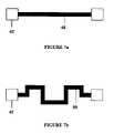
- FIG. 7 ais a schematic of a linear passive trace with terminated resistors.
- FIG. 7 bis a schematic of a serpentine passive trace with terminated resistors.
- FIG. 8is a schematic of a resistor embedded in a via between two circuit layers.
- FIG. 9depicts a method for depositing a coating on the walls and bottom of a via.
- FIGS. 10 a - care schematics using the M 3 D® process in a hybrid additive/subtractive technique to fabricate precision metal structures using an etch resist.
- the M 3 D® processis an additive direct printing technology that operates in an ambient environment, and eliminates the need for lithographic or vacuum deposition techniques.
- the methodis capable of depositing a passive electronic component in a predetermined pattern, and uses aerodynamic focusing of an aerosol stream to deposit patterns onto a planar or non-planar target without the use of masks or modified environments.
- the M 3 D® methodis compatible with commercial thick film and polymer thick film paste compositions, and may also be used with liquid precursor-based formulations, particle-based formulations, and formulations consisting of a combination of particles and liquid precursors.
- the methodis also capable of depositing multiple formulations onto the same target layer. This capability enables direct deposition of resistive structures with a large range of resistance values—ranging from under 50 ⁇ /square to over 500 K ⁇ /square—onto the same layer.
- the M 3 D® methodis capable of blending different formulations, for example one low-value and one high-value composition, in-transit, in a method in which multiple atomizers are preferably used to aerosolize the two compositions.
- the formulationsare preferably deposited through a single deposition head, and blending may occur during aerosol transport, or when the aerosol droplets combine on the target.
- This methodallows for automated tailoring of a formulation, allowing for the resistivity, or other electrical, thermal, optical, or chemical property of the deposit, to be continuously varied from the low value to the high value.
- the blending processcan also be applied to pastes, inks, various fluids (including, but not limited to, chemical precursor solutions, particle suspensions of electronic, optical, biological and bio-compatible materials, adhesives), and combinations thereof.
- passive structuremeans a structure having a desired electrical, magnetic, or other property, including but not limited to a conductor, resistor, capacitor, inductor, insulator, dielectric, suppressor, filter, varistor, ferromagnet, adhesive, and the like.
- the M 3 DTM processpreferably deposits material in an aerosolized form. Aerosolization of most particle suspensions is peferably performed using a pneumatic device, such as a nebulizer, however ultrasonic aerosolization may be used for particle suspensions consisting of small particles or low-density particles. In this case, the solid particles may be suspended in water or an organic solvent and additives that maintain the suspension.
- the two atomization methodsallow for the generation of droplets or droplet/particles with sizes typically in, but not limited to, the 1-5 micron size range.
- Ultrasonically aerosolized compositionstypically have viscosities ranging from 1-10 cP.
- Precursor and precursor/particle compositionstypically have viscosities of 10-100 cP, and are preferably aerosolized pneumatically.
- Compositions with viscosities of 100-1000 cPare also preferably pneumatically aerosolized.
- compositions with viscosities greater than 1000 cPmay be modified to a viscosity suitable for pneumatic aerosolization.
- FIG. 1 ashows the M 3 D® apparatus configured for pneumatic atomization, and details the most general embodiment of the apparatus.
- An inert carrier gas or carrier fluidis preferably used to deliver the aerosolized sample to the deposition module.
- the aerosol-laden carrier gaspreferably enters the deposition head immediately after the aerosolization process.
- the carrier gasmay comprise compressed air, an inert gas (which may comprise a solvent vapor), or a mixture of both.
- the pneumatic aerosolization processrequires a carrier gas flow rate that preferably exceeds the maximum allowable gas flow rate through deposition head 22 .
- a virtual impactoris preferably used to reduce the flowrate of the carrier gas, without appreciable loss of particles or droplets.
- the number of stages used in the virtual impactormay vary, and is dependent on the amount of carrier gas that must be removed.
- the streamis introduced into the M 3 D® deposition head, where an annular flow is developed, consisting of an inner aerosol stream surrounded by a sheath gas.
- the co-flowing configurationis capable of focusing the aerosol stream to approximately one-tenth the size of the orifice diameter.
- the aerosol streamWhen fabricating passive structures using an annular flow, the aerosol stream preferably enters through ports mounted on deposition head 22 and is directed towards the orifice. Aerosol carrier gas flow controller 10 preferably controls the mass throughput. Inside the deposition head, the aerosol stream is preferably initially collimated by passing through a millimeter-size orifice. The emergent particle stream is then combined with a sheath gas or fluid, forming an annular distribution consisting of an inner aerosol-laden carrier gas and an outer sheath gas or fluid.
- the sheath gasmost commonly comprises compressed air or an inert gas, where one or both may contain a modified solvent vapor content. The sheath gas enters through the sheath air inlet below the aerosol inlet and forms an annular flow with the aerosol stream.
- Gas flow controller 12preferably controls the sheath gas.
- the combined streamsexit the chamber through an orifice directed at target 28 .
- This annular flowfocuses the aerosol stream onto target 28 and allows for deposition of features with dimensions as small as 10 microns or lower.
- the purpose of the sheath gasis to form a boundary layer that both focuses the aerosol stream and prevents particles from depositing onto the orifice wall. This shielding effect minimizes clogging of the orifices.
- the diameter of the emerging stream(and therefore the linewidth of the deposit) is controlled by the orifice size, the ratio of sheath gas flow rate to carrier gas flow rate, and the spacing between the orifice and target 28 .
- target 28is attached to a platen that moves in two orthogonal directions under computer control via X-Y linear stages, so that intricate geometries may be deposited.
- An alternate configurationallows for deposition head 22 to move in two orthogonal directions while maintaining target 28 in a fixed position.
- Yet another configurationallows for movement of deposition head 22 in one direction, while target 28 moves in a direction orthogonal to that of deposition head 22 .
- the processalso enables the deposition of three-dimensional structures.
- the M 3 D® methodIn the M 3 D® method, once the sheath gas is combined with the aerosol stream, the flow does not need to pass through more than one orifice in order to deposit sub-millimeter linewidths.
- the M 3 D® methodIn the deposition of a 10-micron line, the M 3 D® method typically achieves a flow diameter constriction of approximately 250, and may be capable of constrictions in excess of 1000, for this “single-stage” deposition. No axial constrictors are used, and the flows typically do not reach supersonic flow velocities, thus preventing the formation of turbulent flow, which could potentially lead to a complete constriction of the flow.
- Collison-type pneumatic atomizer 32aerosolizes the material in the sample vial.
- the aerosol-laden gas streamis delivered to cross 30 that bridges atomizer 32 , deposition head 22 , exhaust flow controller 34 , and pressure sensing transducer 36 .
- Cross 30is preferably configured so that the aerosol flow inlet is opposite the aerosol flow outlet.
- the outletis connected to the M 3 D® deposition head.
- Excess carrier gasis preferably exhausted from the system 90° from the aerosol inlet/outlet line of travel.
- Mass flow controller 34is preferably used to control the amount of gas that is exhausted from the system. Controlling the exhaust flow using a flow controller increases the precision of the deposition process by aiding in the control of the mass flux of the material that passes to the deposition head.
- the atomizeris located directly adjacent to the virtual impactor. Positioning the virtual impactor near the pneumatic atomizer output results in the deposition of larger droplets, since the aerosol ultimately spends less time in transit from the atomizer to the target, and undergoes reduced evaporation.
- the deposition of larger dropletscan produce a considerable effect on the characteristics of the deposited structure. In general, deposited structures formed from larger droplets show less particle overspray and improved edge definition when compared with structures deposited with small to moderate size droplets.
- the atomizeris optionally agitated to prevent material agglomeration.
- the carrier gas flowrate needed for pneumatic atomizationmust be reduced after the aerosol is generated, in order for the aerosol stream to be introduced into the deposition head.
- a virtual impactormay cause the system to be prone to clogging, decreasing the operating time of the apparatus to as little as several minutes, while undesirably decreasing the tolerance of the deposited structure.
- the apparatus of FIG. 1 bmay deposit carbon-based resistors for as little as 15 minutes before failure, with a tolerance in the resistance values of as much as 30%.
- Cross 30acts as a virtual impactor with considerably larger jet and collector orifice diameters than those used with the standard impactor. The use of larger jet and collector orifice diameters may increase the amount of material that flows through the virtual impactor minor flow axis, while minimizing the accumulation of material on the interior of the device.
- the present inventionpreferably uses a leak/clog sensor comprising pressure transducers to monitor the pressure developed at the atomizer gas inlet and at the sheath gas inlet.
- the pressure developed within the systemis related to the total gas flow rate through the system, and can be calculated using a second-order polynomial equation.
- a plot of pressure versus total flow through the systemis shown in FIG. 2 . If the system pressure is higher than the pressure predicted by the curve of FIG. 2 , a non-ideal flow may have developed within the system as a result of material accumulation. If the pressure is too low, a system leak is present, and material deposition may be inhibited or stopped entirely.
- Q pneumaticF sheath +F pneumatic ⁇ F exhaust where F is the device flow rate.
- the coefficients M 0 , M 1 , and M 2are constants for each deposition tip diameter, but are variable with respect to atmospheric pressure.
- the leak/clog sensorprovides a valuable system diagnostic that can allow for continuous manual or automated monitoring and control of the system.
- the systemmay be monitored for clogs, and automatically purged when an increase in pressure beyond a pre-determined value is detected.
- Quantitative measurement of the amount of aerosol generated by the atomizer unitsis critical for extended manual or automated operation of the M 3 D® system. Maintenance of a constant mist density allows for precision deposition, since the mass flux of aerosolized material delivered to the target can be monitored and controlled.
- the system of the present inventionpreferably utilizes a mist sensor, which preferably comprises a visible wavelength laser whose beam passed through the aerosol outlet tube of the atomizer unit.
- the beamis preferably oriented perpendicular to the axis of the tube, and silicon photodiodes are preferably positioned adjacent to the tube on an axis perpendicular to both the axes of the tube and the laser.
- silicon photodiodesare preferably positioned adjacent to the tube on an axis perpendicular to both the axes of the tube and the laser.
- the energy detected by the photodiodesis proportional to the aerosol density of the mist flow.
- the mist flow rateincreases, the photodiode output increases until a state of saturation is reached, at which the photodiode output becomes constant.
- a saturated mist level conditionis preferred for constant mist output, so that a constant photodiode output indicates an optimum operating condition.
- the output of the photodiodesis monitored and can be used to determine the input power to the ultrasonic atomizer transducer.
- the aerosolized material compositionsmay be processed in-flight—during transport to the deposition head 22 (pre-processing)—or once deposited on the target 28 (post-processing).
- Pre-processingmay include, but is not limited to, humidifying or drying the aerosol carrier gas or the sheath gas.
- the humidification processmay be accomplished by introducing aerosolized droplets and/or vapor into the carrier gas flow.
- the evaporation processis preferably accomplished using a heating assembly to evaporate one or more of the solvent and additives.
- Post-processingmay include, but is not limited to using one or a combination of the following processes: (1) thermally heating the deposited feature, (2) subjecting the deposited feature to a reduced pressure atmosphere, or (3) irradiating the feature with electromagnetic radiation.
- Post-processing of passive structuresgenerally requires temperatures ranging from approximately 25 to 1000° C.
- Deposits requiring solvent evaporation or cross-linkingare typically processed at temperatures of approximately 25 to 250° C.
- Precursor or nanoparticle-based depositstypically require processing temperatures of approximately 75 to 600° C., while commercial fireable pastes require more conventional firing temperatures of approximately 450 to 1000° C.
- Commercial polymer thick film pastesare typically processed at temperatures of approximately 25° to 250° C.
- Post-processingmay optionally take place in an oxidizing environment or a reducing environment. Subjecting the deposit to a reduced pressure environment before or during the heating step, in order to aid in the removal of solvents and other volatile additives, may facilitate processing of passive structures on heat-sensitive targets.
- Two preferred methods of reaching the required processing temperaturesare by heating the deposit and target on a heated platen or in a furnace (thermal processing), or by irradiating the feature with laser radiation.
- Laser heating of the depositallows for densification of traditional thick film pastes on heat-sensitive targets.
- Laser photochemical processinghas also been used to decompose liquid precursors to form mid to high-range resistors, low to mid-range dielectric films, and highly conductive metal.
- Laser processingmay optionally be performed simultaneously with deposition. Simultaneous deposition and processing can be used to deposit structures with thicknesses greater than several microns, or to build three-dimensional structures. More details on laser processing may be found in commonly-owned U.S.
- Thermally processed structureshave linewidths that are partially determined by the deposition head and the deposition parameters, and have a minimum linewidth of approximately 5 microns.
- the maximum single pass linewidthis approximately 200 microns.
- Linewidths greater than 200 micronsmay be obtained using a rastered deposition technique.
- Laser-processed linesmay have linewidths ranging from approximately 1 to 100 microns (for a structure deposited with a single pass). Linewidths greater than 100 microns may be obtained using a rastered processing technique.
- laser processingis used to densify or to convert films deposited on heat-sensitive targets, such as those with low temperature thresholds of 400° C. or less, or when a linewidth of less than approximately 5 microns is desired. Deposition of the aerosol stream and processing may occur simultaneously.
- the present inventionprovides a method for precision fabrication of passive structures, wherein the material composition includes, but is not limited to, liquid chemical precursors, inks, pastes, or any combination thereof.
- the present inventioncan deposit electronic materials including but not limited to conductors, resistors, dielectrics, and ferromagnetic materials.
- Metal systemsinclude, but are not limited to, silver, copper, gold, platinum, and palladium, which may be in commercially available paste form.
- Resistor compositionsinclude, but are not limited to, systems composed of silver/glass, ruthenates, polymer thick films formulations, and carbon-based formulations.
- Formulations for deposition of capacitive structuresinclude, but are not limited to, barium titanate, barium strontium titanate, aluminum oxide, and tantalum oxide.
- Inductive structureshave been deposited using a manganese/zinc ferrite formulation blended with low-melting temperature glass particles.
- the present inventioncan also blend two uv-curable inks to produce a final composition with a targeted characteristic, such as a specific refractive index.
- a precursoris a chemical formulation consisting of a solute or solutes dissolved in a suitable solvent.
- the systemmay also contain additives that alter the fluid, chemical, physical, or optical properties of the solution.
- Inksmay be comprised of particles, including but not limited to metal nanoparticles or metal nanoparticles with glass inclusions, of an electronic material suspended in a fluid medium.
- Depositable pastesinclude, but are not limited to, commercially available paste formulations for conductive, resistive, dielectric, and inductive systems.
- the present inventioncan also deposit commercially available adhesive pastes.
- a silver/glass resistor formulationmay be composed of a liquid molecular precursor for silver, along with a suspension of glass particles, or silver and glass particles, or silver particles in a liquid precursor for glass.
- a ruthenate systemmay be comprised of conductive ruthenium oxide particles and insulating glass particles, ruthenium oxide particles in a precursor for glass, or a combination of a ruthenium oxide precursor and a precursor for glass or an insulating medium.
- Precursor compositions and some precursor/particle compositionsmay have viscosities of approximately 10 to 100 cP, and may be aerosolized ultrasonically.
- Resistor pastesmay be comprised of either or both of ruthenates, polymer thick film formulations, or carbon-based formulations.
- ruthenate pastestypically consisting of ruthenium oxide and glass particles, having viscosities of 1000 cP or greater, may be diluted with a suitable solvent such as terpineol to a viscosity of 1000 cP or less.
- a suitable solventsuch as terpineol
- Polymer thick film pastesmay also be diluted in a suitable solvent to a similar viscosity, so that pneumatic aerosolization and flow-guidance is enabled.
- carbon-based pastescan be diluted with a solvent such as butyl carbitol to a viscosity of approximately 1000 cP or less. Therefore, many commercial paste compositions with viscosities greater than 1000 cP may be modified and deposited using the M 3 D® process.
- ResistorsRange of Resistance, Repeatability, and Temperature Coefficient of Resistance
- the resistive structures deposited using the M 3 D® processmay comprise a resistance spanning approximately six orders of magnitude, from 1 ohm to 1 Mohm. This range of resistance values may be obtained by depositing the appropriate material with the appropriate geometrical cross-sectional area.
- the tolerance or variance of the resistance valuesdefined as the ratio of the difference in the resistance value of the highest and lowest passive structure and the average resistance value, for a set of deposits—may be as low as 2 percent.
- the temperature coefficient of resistance (TCR) for Ag/glass and ruthenate structuresmay range from approximately ⁇ 50 to ⁇ 100 ppm.
- the present methodis capable of producing a specific electronic, optical, physical, or chemical value of a structure by controlling the geometry of the deposit.
- properties of a structurecan be altered by controlling the cross-sectional area of the structure, as shown in FIGS. 3 a and 3 b .
- Resistance valuesmay be altered by adding material to an existing trace, thereby increasing the cross sectional area of the total trace, thus decreasing the resistance value as material is added to the existing trace.
- This methodis analogous to commonly used laser trimming methods, however material is added rather than removed.
- the additively trimmed passive trace 38is deposited onto the existing passive trace 40 .
- a specific valuemay be obtained by controlling the length of a deposited structure; as shown in FIG.
- the rightmost resistorhas a greater resistance than the middle structure, by virtue of the greater length of resistor material between the contact pads.
- the method of the present inventionmay also be used to add material to a set of traces or between one or more sets of contact pads 42 connected to a pre-existing electronic circuit, as shown in FIGS. 5 a and 5 b .
- Ladder passive traces 44 a - bare added to existing passive trace 40 . This method enables tuning of the circuit to a specific response or characteristic value.
- the methodis also capable of creating passive structures between layers of circuitry by making passive connections in vias, or by wrapping resistor material 46 around the edge of circuit layers, as shown in FIG. 6 .
- the passive structures deposited using the M 3 D® process of the present inventiontypically have linear geometries, such as the linear passive trace 48 shown in FIG. 7 a .
- Other geometriesinclude, but are not limited to, serpentine 50 (as shown in FIG. 7 b ), spiral, and helical patterns.
- Linewidths of deposited resistor materialtypically range from approximately 10 to 200 microns, but could be greater or lower. Linewidths greater than 200 microns may be obtained by depositing material in a rastered fashion. The thickness of the deposited film may range from a few hundred nanometers to several microns.
- the M 3 D® processcan be used to fill vias, providing electrical interconnectivity between adjacent layers of an electronic circuit.
- the present inventionallows for the precise, uniform deposition of an aerosolized material over an extended period of time, for example into via holes.
- FIG. 8shows a resistive connection between different layers of circuitry.
- Conductive layers in a PCBprinted circuit board
- the M 3 D® processalso allows for deposition of resistive structures into vias.
- the resistive via configurationis advantageous since, by moving the layer resistors into vias, additional space is provided on the surface of the circuit board layers.
- FIG. 9depicts a method for depositing a coating on the walls and bottom of a via.
- via 60is completely filled with ink 62 using the process of the present invention.
- ink 62dries, the solids 64 will adhere onto the walls and the bottom of the via, leaving the middle of the via hollow, as shown in FIG. 9 b .
- Coating the wall with highly conductive materialresults in a very useful structure, because most of the current in a via flows along the wall and not through the middle.
- an inkcan be comprised of a precursor for an insulator, such as polyimide, while a paste may be a formulation containing dielectric particles and low melting temperature glass inclusions.
- the precision deposition offered by the present inventionis critical to fabrication of high tolerance capacitors, since the thickness and uniformity of a capacitive film determines the capacitance and the performance of the capacitor.
- Low-k dielectric materialssuch as glass and polyimide have been deposited for dielectric layers in capacitor applications, and as insulation or passivation layers deposited to isolate electronic components.
- Mid-k and high-k dielectricssuch as barium titanate can be deposited for capacitor applications.
- the present embodiment of the M 3 D® processmay be used in a hybrid additive/subtractive technique to fabricate precision metal structures using an etch resist.
- Etch resist 70is preferably atomized and deposited through the deposition head onto metal layer 72 , as shown in FIG. 10 a .
- a subtractive techniquefor example etching, is then used to remove the exposed metal, FIG. 10 b .
- the etch resistis removed, leaving metal structure 74 on the underlying substrate, FIG. 10 c .
- the additive/subtractive etch resist processcan be used to deposit reactive metals such as copper.
- Targets suitable for direct write of passive structures using the M 3 D® processinclude, but are not limited to, polyimide, FR4, alumina, glass, zirconia, and silicon. Processing of resistor formulations on polyimide, FR4, and other targets with low temperature damage thresholds, i.e. damage thresholds of approximately 400° C. or less, generally requires laser heating to obtain suitable densification. Laser photochemical processing may be used to direct write mid to high range resistor materials such as strontium ruthenate on polyimide.
- M 3 D® processesinclude, but are not limited to, direct write resistors for electronic circuits, heating elements, thermistors, and strain gauges.
- the structuresmay be printed on the more conventional high-temperature targets such as alumina and zirconia, but may also be printed on heat-sensitive targets such as polyimide and FR4.
- the M 3 D® processmay also be used to print embedded passive structures onto pre-existing circuit boards, onto planar or non-planar surfaces, and into vias connecting several layers of a three-dimensional electronic circuit.
- Other applicationsinclude, but are not limited to, blending passive element formulations to produce a deposited structure with a specific physical, optical, electrical, or chemical property; repair of passive structures on pre-populated circuit boards; and deposition of passive structures onto pre-populated targets for the purpose of altering the physical, optical, electrical, or chemical performance of a system.
- the present inventionenables the above applications with tolerances in physical or electrical properties of 5% or less.
Landscapes
- Engineering & Computer Science (AREA)
- Manufacturing & Machinery (AREA)
- Microelectronics & Electronic Packaging (AREA)
- Physics & Mathematics (AREA)
- Condensed Matter Physics & Semiconductors (AREA)
- General Physics & Mathematics (AREA)
- Computer Hardware Design (AREA)
- Power Engineering (AREA)
- Other Surface Treatments For Metallic Materials (AREA)
- Application Of Or Painting With Fluid Materials (AREA)
- Nozzles (AREA)
- Manufacturing Of Printed Wiring (AREA)
Abstract
Description
P=M0+M1Q+M2Q2
where P is the sheath gas pressure and Q is the total flow rate. The total flow rate through the system is given by:
Qultrasonic=Fsheath+Fultrasonic
Qpneumatic=Fsheath+Fpneumatic−Fexhaust
where F is the device flow rate. The coefficients M0, M1, and M2are constants for each deposition tip diameter, but are variable with respect to atmospheric pressure.
Claims (11)
Priority Applications (7)
| Application Number | Priority Date | Filing Date | Title |
|---|---|---|---|
| US11/302,481US7674671B2 (en) | 2004-12-13 | 2005-12-12 | Aerodynamic jetting of aerosolized fluids for fabrication of passive structures |
| JP2007545735AJP5213452B2 (en) | 2004-12-13 | 2005-12-13 | Method and apparatus for aerodynamic injection of aerosolized fluid to produce a passive structure |
| CN2005800426893ACN101142677B (en) | 2004-12-13 | 2005-12-13 | Apparatus and method for depositing passive structures on a target |
| PCT/US2005/045407WO2006065986A2 (en) | 2004-12-13 | 2005-12-13 | Aerodynamic jetting of aerosolized fluids for fabrication of passive structures |
| KR1020077016167AKR101150502B1 (en) | 2004-12-13 | 2005-12-13 | Aerodynamic jetting of aerosolized fluids for fabrication of passive structures |
| US12/720,573US8796146B2 (en) | 2004-12-13 | 2010-03-09 | Aerodynamic jetting of blended aerosolized materials |
| US14/449,811US9607889B2 (en) | 2004-12-13 | 2014-08-01 | Forming structures using aerosol jet® deposition |
Applications Claiming Priority (2)
| Application Number | Priority Date | Filing Date | Title |
|---|---|---|---|
| US63584804P | 2004-12-13 | 2004-12-13 | |
| US11/302,481US7674671B2 (en) | 2004-12-13 | 2005-12-12 | Aerodynamic jetting of aerosolized fluids for fabrication of passive structures |
Related Child Applications (1)
| Application Number | Title | Priority Date | Filing Date |
|---|---|---|---|
| US12/720,573ContinuationUS8796146B2 (en) | 2004-12-13 | 2010-03-09 | Aerodynamic jetting of blended aerosolized materials |
Publications (2)
| Publication Number | Publication Date |
|---|---|
| US20060163570A1 US20060163570A1 (en) | 2006-07-27 |
| US7674671B2true US7674671B2 (en) | 2010-03-09 |
Family
ID=36588543
Family Applications (3)
| Application Number | Title | Priority Date | Filing Date |
|---|---|---|---|
| US11/302,481Expired - Fee RelatedUS7674671B2 (en) | 2004-12-13 | 2005-12-12 | Aerodynamic jetting of aerosolized fluids for fabrication of passive structures |
| US12/720,573ActiveUS8796146B2 (en) | 2004-12-13 | 2010-03-09 | Aerodynamic jetting of blended aerosolized materials |
| US14/449,811ActiveUS9607889B2 (en) | 2004-12-13 | 2014-08-01 | Forming structures using aerosol jet® deposition |
Family Applications After (2)
| Application Number | Title | Priority Date | Filing Date |
|---|---|---|---|
| US12/720,573ActiveUS8796146B2 (en) | 2004-12-13 | 2010-03-09 | Aerodynamic jetting of blended aerosolized materials |
| US14/449,811ActiveUS9607889B2 (en) | 2004-12-13 | 2014-08-01 | Forming structures using aerosol jet® deposition |
Country Status (4)
| Country | Link |
|---|---|
| US (3) | US7674671B2 (en) |
| JP (1) | JP5213452B2 (en) |
| KR (1) | KR101150502B1 (en) |
| WO (1) | WO2006065986A2 (en) |
Cited By (76)
| Publication number | Priority date | Publication date | Assignee | Title |
|---|---|---|---|---|
| US20060008590A1 (en)* | 1998-09-30 | 2006-01-12 | Optomec Design Company | Annular aerosol jet deposition using an extended nozzle |
| US20060175431A1 (en)* | 2004-12-13 | 2006-08-10 | Optomec Design Company | Miniature aerosol jet and aerosol jet array |
| US20070154634A1 (en)* | 2005-12-15 | 2007-07-05 | Optomec Design Company | Method and Apparatus for Low-Temperature Plasma Sintering |
| US20090061077A1 (en)* | 2007-08-31 | 2009-03-05 | Optomec, Inc. | Aerosol Jet (R) printing system for photovoltaic applications |
| US20090061089A1 (en)* | 2007-08-30 | 2009-03-05 | Optomec, Inc. | Mechanically Integrated and Closely Coupled Print Head and Mist Source |
| US20090090298A1 (en)* | 2007-08-31 | 2009-04-09 | Optomec, Inc. | Apparatus for Anisotropic Focusing |
| US20090252874A1 (en)* | 2007-10-09 | 2009-10-08 | Optomec, Inc. | Multiple Sheath Multiple Capillary Aerosol Jet |
| US20100310630A1 (en)* | 2007-04-27 | 2010-12-09 | Technische Universitat Braunschweig | Coated surface for cell culture |
| US7879394B1 (en) | 2006-06-02 | 2011-02-01 | Optomec, Inc. | Deep deposition head |
| US20110036403A1 (en)* | 2008-04-28 | 2011-02-17 | Korea Research Institute Of Chemical Technology | Preparation method of organic photovoltaic cell's photoactive layer using aerosol jet printing |
| US7987813B2 (en) | 1998-09-30 | 2011-08-02 | Optomec, Inc. | Apparatuses and methods for maskless mesoscale material deposition |
| US8110247B2 (en) | 1998-09-30 | 2012-02-07 | Optomec Design Company | Laser processing for heat-sensitive mesoscale deposition of oxygen-sensitive materials |
| US8525346B2 (en) | 2009-06-02 | 2013-09-03 | Hsio Technologies, Llc | Compliant conductive nano-particle electrical interconnect |
| US8610265B2 (en) | 2009-06-02 | 2013-12-17 | Hsio Technologies, Llc | Compliant core peripheral lead semiconductor test socket |
| US8618649B2 (en) | 2009-06-02 | 2013-12-31 | Hsio Technologies, Llc | Compliant printed circuit semiconductor package |
| US8758067B2 (en) | 2010-06-03 | 2014-06-24 | Hsio Technologies, Llc | Selective metalization of electrical connector or socket housing |
| US8789272B2 (en) | 2009-06-02 | 2014-07-29 | Hsio Technologies, Llc | Method of making a compliant printed circuit peripheral lead semiconductor test socket |
| US8796146B2 (en) | 2004-12-13 | 2014-08-05 | Optomec, Inc. | Aerodynamic jetting of blended aerosolized materials |
| US8803539B2 (en) | 2009-06-03 | 2014-08-12 | Hsio Technologies, Llc | Compliant wafer level probe assembly |
| US8912812B2 (en) | 2009-06-02 | 2014-12-16 | Hsio Technologies, Llc | Compliant printed circuit wafer probe diagnostic tool |
| US8928344B2 (en) | 2009-06-02 | 2015-01-06 | Hsio Technologies, Llc | Compliant printed circuit socket diagnostic tool |
| US8955216B2 (en) | 2009-06-02 | 2015-02-17 | Hsio Technologies, Llc | Method of making a compliant printed circuit peripheral lead semiconductor package |
| US8955215B2 (en) | 2009-05-28 | 2015-02-17 | Hsio Technologies, Llc | High performance surface mount electrical interconnect |
| US8970031B2 (en) | 2009-06-16 | 2015-03-03 | Hsio Technologies, Llc | Semiconductor die terminal |
| US8981568B2 (en) | 2009-06-16 | 2015-03-17 | Hsio Technologies, Llc | Simulated wirebond semiconductor package |
| US8981809B2 (en) | 2009-06-29 | 2015-03-17 | Hsio Technologies, Llc | Compliant printed circuit semiconductor tester interface |
| US8988093B2 (en) | 2009-06-02 | 2015-03-24 | Hsio Technologies, Llc | Bumped semiconductor wafer or die level electrical interconnect |
| US8984748B2 (en) | 2009-06-29 | 2015-03-24 | Hsio Technologies, Llc | Singulated semiconductor device separable electrical interconnect |
| US8987886B2 (en) | 2009-06-02 | 2015-03-24 | Hsio Technologies, Llc | Copper pillar full metal via electrical circuit structure |
| US9054097B2 (en) | 2009-06-02 | 2015-06-09 | Hsio Technologies, Llc | Compliant printed circuit area array semiconductor device package |
| US9093767B2 (en) | 2009-06-02 | 2015-07-28 | Hsio Technologies, Llc | High performance surface mount electrical interconnect |
| US9136196B2 (en) | 2009-06-02 | 2015-09-15 | Hsio Technologies, Llc | Compliant printed circuit wafer level semiconductor package |
| US9184145B2 (en) | 2009-06-02 | 2015-11-10 | Hsio Technologies, Llc | Semiconductor device package adapter |
| US9184527B2 (en) | 2009-06-02 | 2015-11-10 | Hsio Technologies, Llc | Electrical connector insulator housing |
| US9196980B2 (en) | 2009-06-02 | 2015-11-24 | Hsio Technologies, Llc | High performance surface mount electrical interconnect with external biased normal force loading |
| US9232654B2 (en) | 2009-06-02 | 2016-01-05 | Hsio Technologies, Llc | High performance electrical circuit structure |
| US9231328B2 (en) | 2009-06-02 | 2016-01-05 | Hsio Technologies, Llc | Resilient conductive electrical interconnect |
| US9254535B2 (en) | 2014-06-20 | 2016-02-09 | Velo3D, Inc. | Apparatuses, systems and methods for three-dimensional printing |
| US9276339B2 (en) | 2009-06-02 | 2016-03-01 | Hsio Technologies, Llc | Electrical interconnect IC device socket |
| US9276336B2 (en) | 2009-05-28 | 2016-03-01 | Hsio Technologies, Llc | Metalized pad to electrical contact interface |
| US9277654B2 (en) | 2009-06-02 | 2016-03-01 | Hsio Technologies, Llc | Composite polymer-metal electrical contacts |
| US9320144B2 (en) | 2009-06-17 | 2016-04-19 | Hsio Technologies, Llc | Method of forming a semiconductor socket |
| US9318862B2 (en) | 2009-06-02 | 2016-04-19 | Hsio Technologies, Llc | Method of making an electronic interconnect |
| US9320133B2 (en) | 2009-06-02 | 2016-04-19 | Hsio Technologies, Llc | Electrical interconnect IC device socket |
| US9350093B2 (en) | 2010-06-03 | 2016-05-24 | Hsio Technologies, Llc | Selective metalization of electrical connector or socket housing |
| US9414500B2 (en) | 2009-06-02 | 2016-08-09 | Hsio Technologies, Llc | Compliant printed flexible circuit |
| US9536815B2 (en) | 2009-05-28 | 2017-01-03 | Hsio Technologies, Llc | Semiconductor socket with direct selective metalization |
| US9559447B2 (en) | 2015-03-18 | 2017-01-31 | Hsio Technologies, Llc | Mechanical contact retention within an electrical connector |
| US9603249B2 (en) | 2009-06-02 | 2017-03-21 | Hsio Technologies, Llc | Direct metalization of electrical circuit structures |
| US9613841B2 (en) | 2009-06-02 | 2017-04-04 | Hsio Technologies, Llc | Area array semiconductor device package interconnect structure with optional package-to-package or flexible circuit to package connection |
| US9662840B1 (en) | 2015-11-06 | 2017-05-30 | Velo3D, Inc. | Adept three-dimensional printing |
| US9689897B2 (en) | 2010-06-03 | 2017-06-27 | Hsio Technologies, Llc | Performance enhanced semiconductor socket |
| US9699906B2 (en) | 2009-06-02 | 2017-07-04 | Hsio Technologies, Llc | Hybrid printed circuit assembly with low density main core and embedded high density circuit regions |
| US9761520B2 (en) | 2012-07-10 | 2017-09-12 | Hsio Technologies, Llc | Method of making an electrical connector having electrodeposited terminals |
| US20180015730A1 (en)* | 2016-07-14 | 2018-01-18 | Integrated Deposition Solutions, Inc. | Apparatuses and Methods for Stable Aerosol-Based Printing Using an Internal Pneumatic Shutter |
| US9919360B2 (en) | 2016-02-18 | 2018-03-20 | Velo3D, Inc. | Accurate three-dimensional printing |
| US9930775B2 (en) | 2009-06-02 | 2018-03-27 | Hsio Technologies, Llc | Copper pillar full metal via electrical circuit structure |
| US9962767B2 (en) | 2015-12-10 | 2018-05-08 | Velo3D, Inc. | Apparatuses for three-dimensional printing |
| US20180126649A1 (en) | 2016-11-07 | 2018-05-10 | Velo3D, Inc. | Gas flow in three-dimensional printing |
| US10086432B2 (en) | 2014-12-10 | 2018-10-02 | Washington State University | Three dimensional sub-mm wavelength sub-THz frequency antennas on flexible and UV-curable dielectric using printed electronic metal traces |
| US10144176B1 (en) | 2018-01-15 | 2018-12-04 | Velo3D, Inc. | Three-dimensional printing systems and methods of their use |
| US10159154B2 (en) | 2010-06-03 | 2018-12-18 | Hsio Technologies, Llc | Fusion bonded liquid crystal polymer circuit structure |
| US10252336B2 (en) | 2016-06-29 | 2019-04-09 | Velo3D, Inc. | Three-dimensional printing and three-dimensional printers |
| US10272525B1 (en) | 2017-12-27 | 2019-04-30 | Velo3D, Inc. | Three-dimensional printing systems and methods of their use |
| US20190143678A1 (en)* | 2017-11-13 | 2019-05-16 | Optomec, Inc. | Shuttering of Aerosol Streams |
| US10315252B2 (en) | 2017-03-02 | 2019-06-11 | Velo3D, Inc. | Three-dimensional printing of three-dimensional objects |
| US10449696B2 (en) | 2017-03-28 | 2019-10-22 | Velo3D, Inc. | Material manipulation in three-dimensional printing |
| US10506722B2 (en) | 2013-07-11 | 2019-12-10 | Hsio Technologies, Llc | Fusion bonded liquid crystal polymer electrical circuit structure |
| US10611092B2 (en) | 2017-01-05 | 2020-04-07 | Velo3D, Inc. | Optics in three-dimensional printing |
| US10667410B2 (en) | 2013-07-11 | 2020-05-26 | Hsio Technologies, Llc | Method of making a fusion bonded circuit structure |
| US10994473B2 (en) | 2015-02-10 | 2021-05-04 | Optomec, Inc. | Fabrication of three dimensional structures by in-flight curing of aerosols |
| US11691343B2 (en) | 2016-06-29 | 2023-07-04 | Velo3D, Inc. | Three-dimensional printing and three-dimensional printers |
| US11817588B2 (en) | 2018-10-04 | 2023-11-14 | Carnegie Mellon University | Three-dimensional lattice batteries via additive manufacturing |
| US11999110B2 (en) | 2019-07-26 | 2024-06-04 | Velo3D, Inc. | Quality assurance in formation of three-dimensional objects |
| US12070907B2 (en) | 2016-09-30 | 2024-08-27 | Velo3D | Three-dimensional objects and their formation |
| US12172444B2 (en) | 2021-04-29 | 2024-12-24 | Optomec, Inc. | High reliability sheathed transport path for aerosol jet devices |
Families Citing this family (18)
| Publication number | Priority date | Publication date | Assignee | Title |
|---|---|---|---|---|
| US20050156991A1 (en)* | 1998-09-30 | 2005-07-21 | Optomec Design Company | Maskless direct write of copper using an annular aerosol jet |
| US7108894B2 (en)* | 1998-09-30 | 2006-09-19 | Optomec Design Company | Direct Write™ System |
| CA2412904A1 (en)* | 2000-06-13 | 2001-12-20 | Element Six (Pty) Ltd. | Composite diamond compacts |
| EP3372266B1 (en)* | 2006-10-02 | 2020-01-01 | Philip Morris Products S.a.s. | Continuous high pressure delivery system |
| US7570493B2 (en)* | 2006-11-16 | 2009-08-04 | Sony Ericsson Mobile Communications | Printed circuit board with embedded circuit component |
| BRPI0817649B8 (en)* | 2007-10-02 | 2021-06-22 | Philip Morris Products Sa | method of dispensing a liquid or aerosol to keep a capillary system free from obstruction and system for maintaining a capillary free from obstruction |
| MX2010003438A (en)* | 2007-10-02 | 2010-04-21 | Philip Morris Prod | Biomarkers and methods for determining sensitivity to vascular endothelial growth factor receptor-2 modulators. |
| US8988756B2 (en)* | 2008-01-31 | 2015-03-24 | Ajjer, Llc | Conductive busbars and sealants for chromogenic devices |
| KR101084171B1 (en) | 2009-08-10 | 2011-11-17 | 삼성모바일디스플레이주식회사 | Organic light emitting display device and manufacturing method of organic light emitting display device |
| US9713687B2 (en) | 2012-08-21 | 2017-07-25 | Philip Morris Usa Inc. | Ventilator aerosol delivery system with transition adapter for introducing carrier gas |
| US9908291B2 (en)* | 2013-09-30 | 2018-03-06 | Adobe Systems Incorporated | Smooth 3D printing using multi-stage filaments |
| US20170348903A1 (en)* | 2015-02-10 | 2017-12-07 | Optomec, Inc. | Fabrication of Three-Dimensional Materials Gradient Structures by In-Flight Curing of Aerosols |
| CA2899255A1 (en)* | 2015-07-31 | 2017-01-31 | National Research Council Of Canada | Apparatus and method for aerosol deposition of nanoparticles on a substrate |
| DE202016103464U1 (en)* | 2016-06-29 | 2016-07-19 | SMR Patents S.à.r.l. | Heater, device for applying a heater and exterior rearview mirror with a heater |
| TW201811543A (en)* | 2016-08-10 | 2018-04-01 | 美商阿普托麥克股份有限公司 | Fabrication of three-dimensional materials gradient structures by in-flight curing of aerosols |
| US11454490B2 (en) | 2019-04-01 | 2022-09-27 | General Electric Company | Strain sensor placement |
| US20220088925A1 (en)* | 2020-09-21 | 2022-03-24 | Integrated Deposition Solutions, Inc. | High-definition aerosol printing using an optimized aerosol distribution and aerodynamic lens system |
| EP4395476A4 (en)* | 2021-08-26 | 2025-01-15 | Shennan Circuits Co., Ltd. | Resistor-buried circuit board and processing method |
Citations (170)
| Publication number | Priority date | Publication date | Assignee | Title |
|---|---|---|---|---|
| US3590477A (en) | 1968-12-19 | 1971-07-06 | Ibm | Method for fabricating insulated-gate field effect transistors having controlled operating characeristics |
| US3715785A (en) | 1971-04-29 | 1973-02-13 | Ibm | Technique for fabricating integrated incandescent displays |
| US3808550A (en) | 1969-12-15 | 1974-04-30 | Bell Telephone Labor Inc | Apparatuses for trapping and accelerating neutral particles |
| US3808432A (en) | 1970-06-04 | 1974-04-30 | Bell Telephone Labor Inc | Neutral particle accelerator utilizing radiation pressure |
| US3846661A (en) | 1971-04-29 | 1974-11-05 | Ibm | Technique for fabricating integrated incandescent displays |
| US3854321A (en) | 1973-04-27 | 1974-12-17 | B Dahneke | Aerosol beam device and method |
| US3901798A (en) | 1973-11-21 | 1975-08-26 | Environmental Research Corp | Aerosol concentrator and classifier |
| US3959798A (en) | 1974-12-31 | 1976-05-25 | International Business Machines Corporation | Selective wetting using a micromist of particles |
| US3974769A (en) | 1975-05-27 | 1976-08-17 | International Business Machines Corporation | Method and apparatus for recording information on a recording surface through the use of mists |
| US3982251A (en) | 1974-08-23 | 1976-09-21 | Ibm Corporation | Method and apparatus for recording information on a recording medium |
| US4016417A (en) | 1976-01-08 | 1977-04-05 | Richard Glasscock Benton | Laser beam transport, and method |
| US4019188A (en) | 1975-05-12 | 1977-04-19 | International Business Machines Corporation | Micromist jet printer |
| US4034025A (en) | 1976-02-09 | 1977-07-05 | Martner John G | Ultrasonic gas stream liquid entrainment apparatus |
| US4046074A (en) | 1976-02-02 | 1977-09-06 | International Business Machines Corporation | Non-impact printing system |
| US4046073A (en) | 1976-01-28 | 1977-09-06 | International Business Machines Corporation | Ultrasonic transfer printing with multi-copy, color and low audible noise capability |
| US4092535A (en) | 1977-04-22 | 1978-05-30 | Bell Telephone Laboratories, Incorporated | Damping of optically levitated particles by feedback and beam shaping |
| US4112437A (en) | 1977-06-27 | 1978-09-05 | Eastman Kodak Company | Electrographic mist development apparatus and method |
| US4132894A (en) | 1978-04-04 | 1979-01-02 | The United States Of America As Represented By The United States Department Of Energy | Monitor of the concentration of particles of dense radioactive materials in a stream of air |
| US4171096A (en) | 1977-05-26 | 1979-10-16 | John Welsh | Spray gun nozzle attachment |
| US4200660A (en) | 1966-04-18 | 1980-04-29 | Firmenich & Cie. | Aromatic sulfur flavoring agents |
| US4228440A (en) | 1977-12-22 | 1980-10-14 | Ricoh Company, Ltd. | Ink jet printing apparatus |
| US4269868A (en) | 1979-03-30 | 1981-05-26 | Rolls-Royce Limited | Application of metallic coatings to metallic substrates |
| US4323756A (en) | 1979-10-29 | 1982-04-06 | United Technologies Corporation | Method for fabricating articles by sequential layer deposition |
| US4453803A (en) | 1981-06-25 | 1984-06-12 | Agency Of Industrial Science & Technology | Optical waveguide for middle infrared band |
| US4485387A (en) | 1982-10-26 | 1984-11-27 | Microscience Systems Corp. | Inking system for producing circuit patterns |
| US4497692A (en) | 1983-06-13 | 1985-02-05 | International Business Machines Corporation | Laser-enhanced jet-plating and jet-etching: high-speed maskless patterning method |
| US4601921A (en) | 1984-12-24 | 1986-07-22 | General Motors Corporation | Method and apparatus for spraying coating material |
| US4605574A (en) | 1981-09-14 | 1986-08-12 | Takashi Yonehara | Method and apparatus for forming an extremely thin film on the surface of an object |
| US4670135A (en) | 1986-06-27 | 1987-06-02 | Regents Of The University Of Minnesota | High volume virtual impactor |
| US4689052A (en) | 1986-02-19 | 1987-08-25 | Washington Research Foundation | Virtual impactor |
| US4825299A (en) | 1986-08-29 | 1989-04-25 | Hitachi, Ltd. | Magnetic recording/reproducing apparatus utilizing phase comparator |
| US4826583A (en) | 1986-09-25 | 1989-05-02 | Lasers Applications Belgium, En Abrege Label S.A. | Apparatus for pinpoint laser-assisted electroplating of metals on solid substrates |
| EP0331022A2 (en) | 1988-03-01 | 1989-09-06 | Texas Instruments Incorporated | Radiation induced pattern deposition |
| US4893886A (en) | 1987-09-17 | 1990-01-16 | American Telephone And Telegraph Company | Non-destructive optical trap for biological particles and method of doing same |
| US4904621A (en) | 1987-07-16 | 1990-02-27 | Texas Instruments Incorporated | Remote plasma generation process using a two-stage showerhead |
| US4911365A (en) | 1989-01-26 | 1990-03-27 | James E. Hynds | Spray gun having a fanning air turbine mechanism |
| US4920254A (en) | 1988-02-22 | 1990-04-24 | Sierracin Corporation | Electrically conductive window and a method for its manufacture |
| US4947463A (en) | 1988-02-24 | 1990-08-07 | Agency Of Industrial Science & Technology | Laser spraying process |
| US4997809A (en) | 1987-11-18 | 1991-03-05 | International Business Machines Corporation | Fabrication of patterned lines of high Tc superconductors |
| US5032850A (en) | 1989-12-18 | 1991-07-16 | Tokyo Electric Co., Ltd. | Method and apparatus for vapor jet printing |
| US5043548A (en) | 1989-02-08 | 1991-08-27 | General Electric Company | Axial flow laser plasma spraying |
| EP0444550A2 (en) | 1990-03-02 | 1991-09-04 | Fried. Krupp AG Hoesch-Krupp | Apparatus for supplying powder filler materials in a welding zone |
| US5064685A (en) | 1989-08-23 | 1991-11-12 | At&T Laboratories | Electrical conductor deposition method |
| US5164535A (en) | 1991-09-05 | 1992-11-17 | Silent Options, Inc. | Gun silencer |
| US5170890A (en) | 1990-12-05 | 1992-12-15 | Wilson Steven D | Particle trap |
| US5176744A (en) | 1991-08-09 | 1993-01-05 | Microelectronics Computer & Technology Corp. | Solution for direct copper writing |
| US5182430A (en) | 1990-10-10 | 1993-01-26 | Societe National D'etude Et De Construction De Moteurs D'aviation "S.N.E.C.M.A." | Powder supply device for the formation of coatings by laser beam treatment |
| US5194297A (en)* | 1992-03-04 | 1993-03-16 | Vlsi Standards, Inc. | System and method for accurately depositing particles on a surface |
| US5208431A (en) | 1990-09-10 | 1993-05-04 | Agency Of Industrial Science & Technology | Method for producing object by laser spraying and apparatus for conducting the method |
| US5245404A (en) | 1990-10-18 | 1993-09-14 | Physical Optics Corportion | Raman sensor |
| US5250383A (en) | 1990-02-23 | 1993-10-05 | Fuji Photo Film Co., Ltd. | Process for forming multilayer coating |
| US5254832A (en) | 1990-01-12 | 1993-10-19 | U.S. Philips Corporation | Method of manufacturing ultrafine particles and their application |
| US5270542A (en) | 1992-12-31 | 1993-12-14 | Regents Of The University Of Minnesota | Apparatus and method for shaping and detecting a particle beam |
| US5292418A (en) | 1991-03-08 | 1994-03-08 | Mitsubishi Denki Kabushiki Kaisha | Local laser plating apparatus |
| US5322221A (en) | 1992-11-09 | 1994-06-21 | Graco Inc. | Air nozzle |
| EP0470911B1 (en) | 1990-08-10 | 1994-07-27 | Roussel-Uclaf | Spraying system |
| US5335000A (en) | 1992-08-04 | 1994-08-02 | Calcomp Inc. | Ink vapor aerosol pen for pen plotters |
| US5344676A (en) | 1992-10-23 | 1994-09-06 | The Board Of Trustees Of The University Of Illinois | Method and apparatus for producing nanodrops and nanoparticles and thin film deposits therefrom |
| US5366559A (en) | 1993-05-27 | 1994-11-22 | Research Triangle Institute | Method for protecting a substrate surface from contamination using the photophoretic effect |
| US5378505A (en) | 1991-02-27 | 1995-01-03 | Honda Giken Kogyo Kabushiki Kaisha | Method of and apparatus for electrostatically spray-coating work with paint |
| US5378508A (en) | 1992-04-01 | 1995-01-03 | Akzo Nobel N.V. | Laser direct writing |
| US5403617A (en) | 1993-09-15 | 1995-04-04 | Mobium Enterprises Corporation | Hybrid pulsed valve for thin film coating and method |
| US5449536A (en) | 1992-12-18 | 1995-09-12 | United Technologies Corporation | Method for the application of coatings of oxide dispersion strengthened metals by laser powder injection |
| US5486676A (en) | 1994-11-14 | 1996-01-23 | General Electric Company | Coaxial single point powder feed nozzle |
| US5495105A (en) | 1992-02-20 | 1996-02-27 | Canon Kabushiki Kaisha | Method and apparatus for particle manipulation, and measuring apparatus utilizing the same |
| US5512745A (en) | 1994-03-09 | 1996-04-30 | Board Of Trustees Of The Leland Stanford Jr. University | Optical trap system and method |
| US5607730A (en) | 1995-09-11 | 1997-03-04 | Clover Industries, Inc. | Method and apparatus for laser coating |
| US5609921A (en) | 1994-08-26 | 1997-03-11 | Universite De Sherbrooke | Suspension plasma spray |
| US5612099A (en) | 1995-05-23 | 1997-03-18 | Mcdonnell Douglas Corporation | Method and apparatus for coating a substrate |
| US5614252A (en) | 1988-12-27 | 1997-03-25 | Symetrix Corporation | Method of fabricating barium strontium titanate |
| US5648127A (en) | 1994-01-18 | 1997-07-15 | Qqc, Inc. | Method of applying, sculpting, and texturing a coating on a substrate and for forming a heteroepitaxial coating on a surface of a substrate |
| US5676719A (en) | 1996-02-01 | 1997-10-14 | Engineering Resources, Inc. | Universal insert for use with radiator steam traps |
| US5733609A (en) | 1993-06-01 | 1998-03-31 | Wang; Liang | Ceramic coatings synthesized by chemical reactions energized by laser plasmas |
| US5736195A (en) | 1993-09-15 | 1998-04-07 | Mobium Enterprises Corporation | Method of coating a thin film on a substrate |
| US5770272A (en) | 1995-04-28 | 1998-06-23 | Massachusetts Institute Of Technology | Matrix-bearing targets for maldi mass spectrometry and methods of production thereof |
| US5772106A (en) | 1995-12-29 | 1998-06-30 | Microfab Technologies, Inc. | Printhead for liquid metals and method of use |
| US5814152A (en) | 1995-05-23 | 1998-09-29 | Mcdonnell Douglas Corporation | Apparatus for coating a substrate |
| US5844192A (en) | 1996-05-09 | 1998-12-01 | United Technologies Corporation | Thermal spray coating method and apparatus |
| US5854311A (en) | 1996-06-24 | 1998-12-29 | Richart; Douglas S. | Process and apparatus for the preparation of fine powders |
| US5861136A (en) | 1995-01-10 | 1999-01-19 | E. I. Du Pont De Nemours And Company | Method for making copper I oxide powders by aerosol decomposition |
| US5882722A (en) | 1995-07-12 | 1999-03-16 | Partnerships Limited, Inc. | Electrical conductors formed from mixtures of metal powders and metallo-organic decompositions compounds |
| US5894403A (en) | 1997-05-01 | 1999-04-13 | Wilson Greatbatch Ltd. | Ultrasonically coated substrate for use in a capacitor |
| US5940099A (en) | 1993-08-15 | 1999-08-17 | Ink Jet Technology, Inc. & Scitex Corporation Ltd. | Ink jet print head with ink supply through porous medium |
| US5958268A (en) | 1995-06-07 | 1999-09-28 | Cauldron Limited Partnership | Removal of material by polarized radiation |
| US5965212A (en) | 1995-07-27 | 1999-10-12 | Isis Innovation Limited | Method of producing metal quantum dots |
| US5980998A (en) | 1997-09-16 | 1999-11-09 | Sri International | Deposition of substances on a surface |
| US5993549A (en) | 1996-01-19 | 1999-11-30 | Deutsche Forschungsanstalt Fuer Luft- Und Raumfahrt E.V. | Powder coating apparatus |
| US5997956A (en) | 1995-08-04 | 1999-12-07 | Microcoating Technologies | Chemical vapor deposition and powder formation using thermal spray with near supercritical and supercritical fluid solutions |
| US6007631A (en) | 1997-11-10 | 1999-12-28 | Speedline Technologies, Inc. | Multiple head dispensing system and method |
| US6015083A (en) | 1995-12-29 | 2000-01-18 | Microfab Technologies, Inc. | Direct solder bumping of hard to solder substrate |
| US6025037A (en) | 1994-04-25 | 2000-02-15 | U.S. Philips Corporation | Method of curing a film |
| US6110144A (en) | 1998-01-15 | 2000-08-29 | Medtronic Ave, Inc. | Method and apparatus for regulating the fluid flow rate to and preventing over-pressurization of a balloon catheter |
| US6116718A (en) | 1998-09-30 | 2000-09-12 | Xerox Corporation | Print head for use in a ballistic aerosol marking apparatus |
| US6136442A (en) | 1998-09-30 | 2000-10-24 | Xerox Corporation | Multi-layer organic overcoat for particulate transport electrode grid |
| US6151435A (en) | 1998-11-01 | 2000-11-21 | The United States Of America As Represented By The Secretary Of The Navy | Evanescent atom guiding in metal-coated hollow-core optical fibers |
| US6159749A (en) | 1998-07-21 | 2000-12-12 | Beckman Coulter, Inc. | Highly sensitive bead-based multi-analyte assay system using optical tweezers |
| US6182688B1 (en) | 1998-06-19 | 2001-02-06 | Aerospatiale Societe Nationale Industrielle | Autonomous device for limiting the rate of flow of a fluid through a pipe, and fuel circuit for an aircraft comprising such a device |
| US6197366B1 (en) | 1997-05-06 | 2001-03-06 | Takamatsu Research Laboratory | Metal paste and production process of metal film |
| US6251488B1 (en) | 1999-05-05 | 2001-06-26 | Optomec Design Company | Precision spray processes for direct write electronic components |
| US6258733B1 (en) | 1996-05-21 | 2001-07-10 | Sand Hill Capital Ii, Lp | Method and apparatus for misted liquid source deposition of thin film with reduced mist particle size |
| US6265050B1 (en) | 1998-09-30 | 2001-07-24 | Xerox Corporation | Organic overcoat for electrode grid |
| US6290342B1 (en) | 1998-09-30 | 2001-09-18 | Xerox Corporation | Particulate marking material transport apparatus utilizing traveling electrostatic waves |
| US6291088B1 (en) | 1998-09-30 | 2001-09-18 | Xerox Corporation | Inorganic overcoat for particulate transport electrode grid |
| US6293659B1 (en) | 1999-09-30 | 2001-09-25 | Xerox Corporation | Particulate source, circulation, and valving system for ballistic aerosol marking |
| US20010046551A1 (en)* | 2000-02-16 | 2001-11-29 | Michael Falck | Strip coating method |
| US6340216B1 (en) | 1998-09-30 | 2002-01-22 | Xerox Corporation | Ballistic aerosol marking apparatus for treating a substrate |
| US20020012743A1 (en) | 2000-07-25 | 2002-01-31 | The Research Foundation Of State University Of New York | Method and apparatus for fine feature spray deposition |
| US6348687B1 (en) | 1999-09-10 | 2002-02-19 | Sandia Corporation | Aerodynamic beam generator for large particles |
| US6349668B1 (en)* | 1998-04-27 | 2002-02-26 | Msp Corporation | Method and apparatus for thin film deposition on large area substrates |
| US6379745B1 (en) | 1997-02-20 | 2002-04-30 | Parelec, Inc. | Low temperature method and compositions for producing electrical conductors |
| US6390115B1 (en) | 1998-05-20 | 2002-05-21 | GSF-Forschungszentrum für Umwelt und Gesundheit | Method and device for producing a directed gas jet |
| US6406137B1 (en) | 1998-12-22 | 2002-06-18 | Canon Kabushiki Kaisha | Ink-jet print head and production method of ink-jet print head |
| US6416159B1 (en) | 1998-09-30 | 2002-07-09 | Xerox Corporation | Ballistic aerosol marking apparatus with non-wetting coating |
| US6416389B1 (en) | 2000-07-28 | 2002-07-09 | Xerox Corporation | Process for roughening a surface |
| US6416157B1 (en) | 1998-09-30 | 2002-07-09 | Xerox Corporation | Method of marking a substrate employing a ballistic aerosol marking apparatus |
| US6416156B1 (en) | 1998-09-30 | 2002-07-09 | Xerox Corporation | Kinetic fusing of a marking material |
| US20020096647A1 (en) | 2000-08-25 | 2002-07-25 | Asm Lithography B.V. | Mask handling apparatus, lithographic projection apparatus, device manufacturing method and device manufactured thereby |
| US20020100416A1 (en) | 2001-01-30 | 2002-08-01 | Sun James J. | Method and apparatus for deposition of particles on surfaces |
| US20020132051A1 (en) | 1995-12-14 | 2002-09-19 | Kwang-Leong Choy | Film or coating deposition and powder formation |
| US6454384B1 (en) | 1998-09-30 | 2002-09-24 | Xerox Corporation | Method for marking with a liquid material using a ballistic aerosol marking apparatus |
| US6467862B1 (en) | 1998-09-30 | 2002-10-22 | Xerox Corporation | Cartridge for use in a ballistic aerosol marking apparatus |
| US6471327B2 (en) | 2001-02-27 | 2002-10-29 | Eastman Kodak Company | Apparatus and method of delivering a focused beam of a thermodynamically stable/metastable mixture of a functional material in a dense fluid onto a receiver |
| US20020162974A1 (en) | 2001-05-03 | 2002-11-07 | Orsini Rocco A. | High temperature EUV source nozzle |
| US20030003241A1 (en) | 2001-06-27 | 2003-01-02 | Matsushita Electric Industrial Co., Ltd. | Depositing method and a surface modifying method for nano-particles in a gas stream |
| US6503831B2 (en) | 1997-10-14 | 2003-01-07 | Patterning Technologies Limited | Method of forming an electronic device |
| US20030020768A1 (en) | 1998-09-30 | 2003-01-30 | Renn Michael J. | Direct write TM system |
| US6513736B1 (en) | 1996-07-08 | 2003-02-04 | Corning Incorporated | Gas-assisted atomizing device and methods of making gas-assisted atomizing devices |
| US6521297B2 (en) | 2000-06-01 | 2003-02-18 | Xerox Corporation | Marking material and ballistic aerosol marking process for the use thereof |
| US20030048314A1 (en) | 1998-09-30 | 2003-03-13 | Optomec Design Company | Direct write TM system |
| US6537501B1 (en) | 1998-05-18 | 2003-03-25 | University Of Washington | Disposable hematology cartridge |
| US6544599B1 (en) | 1996-07-31 | 2003-04-08 | Univ Arkansas | Process and apparatus for applying charged particles to a substrate, process for forming a layer on a substrate, products made therefrom |
| US6548122B1 (en) | 1997-09-16 | 2003-04-15 | Sri International | Method of producing and depositing a metal film |
| US6573491B1 (en) | 1999-05-17 | 2003-06-03 | Rock Mountain Biosystems, Inc. | Electromagnetic energy driven separation methods |
| US20030108664A1 (en) | 2001-10-05 | 2003-06-12 | Kodas Toivo T. | Methods and compositions for the formation of recessed electrical features on a substrate |
| US20030108511A1 (en) | 1998-08-14 | 2003-06-12 | Sawhney Amarpreet S. | Adhesion barriers applicable by minimally invasive surgery and methods of use thereof |
| US20030117691A1 (en) | 2001-12-21 | 2003-06-26 | Xiangxin Bi | Three dimensional engineering of planar optical structures |
| US20030138967A1 (en) | 2002-01-22 | 2003-07-24 | Dakocytomation Denmark A/S | Environmental containment system for a flow cytometer |
| US20030175411A1 (en) | 2001-10-05 | 2003-09-18 | Kodas Toivo T. | Precursor compositions and methods for the deposition of passive electrical components on a substrate |
| US20030180451A1 (en) | 2001-10-05 | 2003-09-25 | Kodas Toivo T. | Low viscosity copper precursor compositions and methods for the deposition of conductive electronic features |
| US6636676B1 (en) | 1998-09-30 | 2003-10-21 | Optomec Design Company | Particle guidance system |
| US20030202043A1 (en) | 2002-04-24 | 2003-10-30 | Huanzhao Zeng | Determination of control points for construction of first color space-to-second color space look-up table |
| US6646253B1 (en) | 1998-05-20 | 2003-11-11 | GSF-Forschungszentrum für Umwelt und Gesundheit GmbH | Gas inlet for an ion source |
| US20030219923A1 (en) | 2002-03-01 | 2003-11-27 | Arokia Nathan | Method and system for fabricating electronics |
| US20030228124A1 (en)* | 1998-09-30 | 2003-12-11 | Renn Michael J. | Apparatuses and method for maskless mesoscale material deposition |
| US20040004209A1 (en) | 2000-10-25 | 2004-01-08 | Yorishige Matsuba | Electroconductive metal paste and method for production thereof |
| US20040029706A1 (en) | 2002-02-14 | 2004-02-12 | Barrera Enrique V. | Fabrication of reinforced composite material comprising carbon nanotubes, fullerenes, and vapor-grown carbon fibers for thermal barrier materials, structural ceramics, and multifunctional nanocomposite ceramics |
| US20040038808A1 (en) | 1998-08-27 | 2004-02-26 | Hampden-Smith Mark J. | Method of producing membrane electrode assemblies for use in proton exchange membrane and direct methanol fuel cells |
| US20040080917A1 (en) | 2002-10-23 | 2004-04-29 | Steddom Clark Morrison | Integrated microwave package and the process for making the same |
| US20040151978A1 (en) | 2003-01-30 | 2004-08-05 | Huang Wen C. | Method and apparatus for direct-write of functional materials with a controlled orientation |
| US20040185388A1 (en) | 2003-01-29 | 2004-09-23 | Hiroyuki Hirai | Printed circuit board, method for producing same, and ink therefor |
| US20040191695A1 (en) | 2003-03-27 | 2004-09-30 | Ray Kevin Barry | Nanopastes as patterning compositions for electronic parts |
| US20040197493A1 (en) | 1998-09-30 | 2004-10-07 | Optomec Design Company | Apparatus, methods and precision spray processes for direct write and maskless mesoscale material deposition |
| US6811805B2 (en) | 2001-05-30 | 2004-11-02 | Novatis Ag | Method for applying a coating |
| US20040247782A1 (en)* | 1997-02-24 | 2004-12-09 | Hampden-Smith Mark J. | Palladium-containing particles, method and apparatus of manufacture, palladium-containing devices made therefrom |
| US6832124B2 (en) | 2000-06-22 | 2004-12-14 | Telefonaktiebolaget Lm Ericsson (Publ) | Method and an arrangement relating to optical fibers |
| US6890624B1 (en) | 2000-04-25 | 2005-05-10 | Nanogram Corporation | Self-assembled structures |
| US20050110064A1 (en) | 2002-09-30 | 2005-05-26 | Nanosys, Inc. | Large-area nanoenabled macroelectronic substrates and uses therefor |
| US20050129383A1 (en) | 1998-09-30 | 2005-06-16 | Optomec Design Company | Laser processing for heat-sensitive mesoscale deposition |
| US20050145968A1 (en) | 2003-11-06 | 2005-07-07 | Rohm And Haas Electronic Materials, L.L.C. | Optical article |
| US20050147749A1 (en) | 2004-01-05 | 2005-07-07 | Msp Corporation | High-performance vaporizer for liquid-precursor and multi-liquid-precursor vaporization in semiconductor thin film deposition |
| US20050156991A1 (en) | 1998-09-30 | 2005-07-21 | Optomec Design Company | Maskless direct write of copper using an annular aerosol jet |
| US20050184328A1 (en) | 2004-02-19 | 2005-08-25 | Matsushita Electric Industrial Co., Ltd. | Semiconductor device and its manufacturing method |
| US20050215689A1 (en) | 2002-06-13 | 2005-09-29 | Arkady Garbar | Nano-powder-based coating and ink compositions |
| US20050214480A1 (en) | 2002-06-13 | 2005-09-29 | Arkady Garbar | Nano-powder-based coating and ink compositions |
| US20050238804A1 (en) | 2002-06-13 | 2005-10-27 | Arkady Garbar | Nano-powder-based coating and ink compositions |
| US20060008590A1 (en) | 1998-09-30 | 2006-01-12 | Optomec Design Company | Annular aerosol jet deposition using an extended nozzle |
| WO2006065978A2 (en) | 2004-12-13 | 2006-06-22 | Optomec Design Company | Miniature aerosol jet and aerosol jet array |
| US20060280866A1 (en) | 2004-10-13 | 2006-12-14 | Optomec Design Company | Method and apparatus for mesoscale deposition of biological materials and biomaterials |
| US20070019028A1 (en) | 1998-09-30 | 2007-01-25 | Optomec Design Company | Laser processing for heat-sensitive mesoscale deposition of oxygen-sensitive materials |
| JP2007507114A (en) | 2003-09-26 | 2007-03-22 | オプトメック・デザイン・カンパニー | Laser treatment of heat sensitive medium scale deposition. |
Family Cites Families (149)
| Publication number | Priority date | Publication date | Assignee | Title |
|---|---|---|---|---|
| US597956A (en)* | 1898-01-25 | Warping-rollefl | ||
| US3474971A (en) | 1967-06-14 | 1969-10-28 | North American Rockwell | Two-piece injector |
| US3642202A (en) | 1970-05-13 | 1972-02-15 | Exxon Research Engineering Co | Feed system for coking unit |
| US3777983A (en) | 1971-12-16 | 1973-12-11 | Gen Electric | Gas cooled dual fuel air atomized fuel nozzle |
| US3816025A (en) | 1973-01-18 | 1974-06-11 | Neill W O | Paint spray system |
| US4036434A (en) | 1974-07-15 | 1977-07-19 | Aerojet-General Corporation | Fluid delivery nozzle with fluid purged face |
| DE2517715C2 (en) | 1975-04-22 | 1977-02-10 | Hans Behr | PROCESS AND DEVICE FOR MIXING AND / OR DISPERSING AND BLASTING THE COMPONENTS OF A FLOWABLE MATERIAL FOR COATING SURFACES |
| US4004733A (en) | 1975-07-09 | 1977-01-25 | Research Corporation | Electrostatic spray nozzle system |
| US4235563A (en) | 1977-07-11 | 1980-11-25 | The Upjohn Company | Method and apparatus for feeding powder |
| US4200669A (en) | 1978-11-22 | 1980-04-29 | The United States Of America As Represented By The Secretary Of The Navy | Laser spraying |
| JPS5948873B2 (en) | 1980-05-14 | 1984-11-29 | ペルメレック電極株式会社 | Method for manufacturing electrode substrate or electrode provided with corrosion-resistant coating |
| US4685563A (en) | 1983-05-16 | 1987-08-11 | Michelman Inc. | Packaging material and container having interlaminate electrostatic shield and method of making same |
| US4694136A (en) | 1986-01-23 | 1987-09-15 | Westinghouse Electric Corp. | Laser welding of a sleeve within a tube |
| US4823009A (en) | 1986-04-14 | 1989-04-18 | Massachusetts Institute Of Technology | Ir compatible deposition surface for liquid chromatography |
| US4733018A (en) | 1986-10-02 | 1988-03-22 | Rca Corporation | Thick film copper conductor inks |
| US4927992A (en) | 1987-03-04 | 1990-05-22 | Westinghouse Electric Corp. | Energy beam casting of metal articles |
| US4724299A (en) | 1987-04-15 | 1988-02-09 | Quantum Laser Corporation | Laser spray nozzle and method |
| US4917830A (en) | 1988-09-19 | 1990-04-17 | The United States Of America As Represented By The United States Department Of Energy | Monodisperse aerosol generator |
| US4971251A (en) | 1988-11-28 | 1990-11-20 | Minnesota Mining And Manufacturing Company | Spray gun with disposable liquid handling portion |
| US6056994A (en)* | 1988-12-27 | 2000-05-02 | Symetrix Corporation | Liquid deposition methods of fabricating layered superlattice materials |
| US5038014A (en) | 1989-02-08 | 1991-08-06 | General Electric Company | Fabrication of components by layered deposition |
| US5017317A (en) | 1989-12-04 | 1991-05-21 | Board Of Regents, The Uni. Of Texas System | Gas phase selective beam deposition |
| US4978067A (en) | 1989-12-22 | 1990-12-18 | Sono-Tek Corporation | Unitary axial flow tube ultrasonic atomizer with enhanced sealing |
| US5176328A (en) | 1990-03-13 | 1993-01-05 | The Board Of Regents Of The University Of Nebraska | Apparatus for forming fin particles |
| US5126102A (en) | 1990-03-15 | 1992-06-30 | Kabushiki Kaisha Toshiba | Fabricating method of composite material |
| CN2078199U (en) | 1990-06-15 | 1991-06-05 | 蒋隽 | Multipurpose protable ultrasonic atomizer |
| US6175422B1 (en) | 1991-01-31 | 2001-01-16 | Texas Instruments Incorporated | Method and apparatus for the computer-controlled manufacture of three-dimensional objects from computer data |
| DE59201161D1 (en) | 1991-02-02 | 1995-02-23 | Theysohn Friedrich Fa | Process for producing a wear-reducing layer. |
| WO1992018323A1 (en) | 1991-04-09 | 1992-10-29 | Haber Michael B | Computerised macro-assembly manufacture |
| US5173220A (en) | 1991-04-26 | 1992-12-22 | Motorola, Inc. | Method of manufacturing a three-dimensional plastic article |
| US5314003A (en) | 1991-12-24 | 1994-05-24 | Microelectronics And Computer Technology Corporation | Three-dimensional metal fabrication using a laser |
| FR2685922B1 (en) | 1992-01-07 | 1995-03-24 | Strasbourg Elec | COAXIAL NOZZLE FOR SURFACE TREATMENT UNDER LASER IRRADIATION, WITH SUPPLY OF MATERIALS IN POWDER FORM. |
| JPH05283708A (en) | 1992-04-02 | 1993-10-29 | Mitsubishi Electric Corp | Nonvolatile semiconductor memory device, manufacturing method and testing method thereof |
| DE69314343T2 (en) | 1992-07-08 | 1998-03-26 | Nordson Corp | DEVICE AND METHOD FOR APPLYING FOAM COATINGS |
| US5294459A (en) | 1992-08-27 | 1994-03-15 | Nordson Corporation | Air assisted apparatus and method for selective coating |
| IL107120A (en) | 1992-09-29 | 1997-09-30 | Boehringer Ingelheim Int | Atomising nozzle and filter and spray generating device |
| JPH08156106A (en) | 1992-11-13 | 1996-06-18 | Japan Atom Energy Res Inst | 3D object manufacturing method |
| US5775402A (en) | 1995-10-31 | 1998-07-07 | Massachusetts Institute Of Technology | Enhancement of thermal properties of tooling made by solid free form fabrication techniques |
| US5529634A (en) | 1992-12-28 | 1996-06-25 | Kabushiki Kaisha Toshiba | Apparatus and method of manufacturing semiconductor device |
| US5359172A (en) | 1992-12-30 | 1994-10-25 | Westinghouse Electric Corporation | Direct tube repair by laser welding |
| US5425802A (en) | 1993-05-05 | 1995-06-20 | The United States Of American As Represented By The Administrator Of Environmental Protection Agency | Virtual impactor for removing particles from an airstream and method for using same |
| US20030203976A1 (en)* | 1993-07-19 | 2003-10-30 | William L. Hunter | Anti-angiogenic compositions and methods of use |
| US5398193B1 (en) | 1993-08-20 | 1997-09-16 | Alfredo O Deangelis | Method of three-dimensional rapid prototyping through controlled layerwise deposition/extraction and apparatus therefor |
| US5491317A (en) | 1993-09-13 | 1996-02-13 | Westinghouse Electric Corporation | System and method for laser welding an inner surface of a tubular member |
| US5518680A (en) | 1993-10-18 | 1996-05-21 | Massachusetts Institute Of Technology | Tissue regeneration matrices by solid free form fabrication techniques |
| US5477026A (en) | 1994-01-27 | 1995-12-19 | Chromalloy Gas Turbine Corporation | Laser/powdered metal cladding nozzle |
| FR2724853B1 (en) | 1994-09-27 | 1996-12-20 | Saint Gobain Vitrage | DEVICE FOR DISPENSING POWDERY SOLIDS ON THE SURFACE OF A SUBSTRATE FOR LAYING A COATING |
| US5732885A (en) | 1994-10-07 | 1998-03-31 | Spraying Systems Co. | Internal mix air atomizing spray nozzle |
| US5541006A (en) | 1994-12-23 | 1996-07-30 | Kennametal Inc. | Method of making composite cermet articles and the articles |
| US5779833A (en) | 1995-08-04 | 1998-07-14 | Case Western Reserve University | Method for constructing three dimensional bodies from laminations |
| US5837960A (en) | 1995-08-14 | 1998-11-17 | The Regents Of The University Of California | Laser production of articles from powders |
| US5746844A (en) | 1995-09-08 | 1998-05-05 | Aeroquip Corporation | Method and apparatus for creating a free-form three-dimensional article using a layer-by-layer deposition of molten metal and using a stress-reducing annealing process on the deposited metal |
| US5653925A (en) | 1995-09-26 | 1997-08-05 | Stratasys, Inc. | Method for controlled porosity three-dimensional modeling |
| US5772964A (en)* | 1996-02-08 | 1998-06-30 | Lab Connections, Inc. | Nozzle arrangement for collecting components from a fluid for analysis |
| CN1093783C (en) | 1996-02-21 | 2002-11-06 | 松下电器产业株式会社 | Liquid spray nozzle and method of manufacturing liquid spray nozzle |
| US5705117A (en) | 1996-03-01 | 1998-01-06 | Delco Electronics Corporaiton | Method of combining metal and ceramic inserts into stereolithography components |
| DE69700945T2 (en) | 1996-04-17 | 2000-07-20 | Koninklijke Philips Electronics N.V., Eindhoven | METHOD FOR PRODUCING A SINTERED STRUCTURE ON A SUBSTRATE |
| US6046426A (en) | 1996-07-08 | 2000-04-04 | Sandia Corporation | Method and system for producing complex-shape objects |
| US5772963A (en) | 1996-07-30 | 1998-06-30 | Bayer Corporation | Analytical instrument having a control area network and distributed logic nodes |
| US5707715A (en) | 1996-08-29 | 1998-01-13 | L. Pierre deRochemont | Metal ceramic composites with improved interfacial properties and methods to make such composites |
| JP3867176B2 (en) | 1996-09-24 | 2007-01-10 | アール・アイ・ディー株式会社 | Powder mass flow measuring device and electrostatic powder coating device using the same |
| US6143116A (en) | 1996-09-26 | 2000-11-07 | Kyocera Corporation | Process for producing a multi-layer wiring board |
| US5742050A (en) | 1996-09-30 | 1998-04-21 | Aviv Amirav | Method and apparatus for sample introduction into a mass spectrometer for improving a sample analysis |
| US6144008A (en) | 1996-11-22 | 2000-11-07 | Rabinovich; Joshua E. | Rapid manufacturing system for metal, metal matrix composite materials and ceramics |
| US5578227A (en) | 1996-11-22 | 1996-11-26 | Rabinovich; Joshua E. | Rapid prototyping system |
| JP3831415B2 (en) | 1997-01-03 | 2006-10-11 | エムディーエス インコーポレーテッド | Spray chamber with dryer |
| US5849238A (en) | 1997-06-26 | 1998-12-15 | Ut Automotive Dearborn, Inc. | Helical conformal channels for solid freeform fabrication and tooling applications |
| JP2987430B2 (en)* | 1997-06-30 | 1999-12-06 | 工業技術院長 | Method for forming and forming ultrafine particles and apparatus therefor |
| US6391494B2 (en) | 1999-05-13 | 2002-05-21 | Nanogram Corporation | Metal vanadium oxide particles |
| US5847357A (en) | 1997-08-25 | 1998-12-08 | General Electric Company | Laser-assisted material spray processing |
| US6021776A (en) | 1997-09-09 | 2000-02-08 | Intertex Research, Inc. | Disposable atomizer device with trigger valve system |
| US5993554A (en) | 1998-01-22 | 1999-11-30 | Optemec Design Company | Multiple beams and nozzles to increase deposition rate |
| US6967183B2 (en)* | 1998-08-27 | 2005-11-22 | Cabot Corporation | Electrocatalyst powders, methods for producing powders and devices fabricated from same |
| US20050097987A1 (en) | 1998-02-24 | 2005-05-12 | Cabot Corporation | Coated copper-containing powders, methods and apparatus for producing such powders, and copper-containing devices fabricated from same |
| US6410105B1 (en) | 1998-06-30 | 2002-06-25 | Jyoti Mazumder | Production of overhang, undercut, and cavity structures using direct metal depostion |
| US6149076A (en) | 1998-08-05 | 2000-11-21 | Nordson Corporation | Dispensing apparatus having nozzle for controlling heated liquid discharge with unheated pressurized air |
| KR100271208B1 (en) | 1998-08-13 | 2000-12-01 | 윤덕용 | Selective infiltration manufacturing method and apparatus |
| DE19841401C2 (en) | 1998-09-10 | 2000-09-21 | Lechler Gmbh & Co Kg | Two-component flat jet nozzle |
| JP2002528744A (en) | 1998-09-30 | 2002-09-03 | ボード・オブ・コントロール・オブ・ミシガン・テクノロジカル・ユニバーシティ | Laser guided operation of non-atomic particles |
| US6001304A (en) | 1998-12-31 | 1999-12-14 | Materials Modification, Inc. | Method of bonding a particle material to near theoretical density |
| KR100284607B1 (en) | 1998-12-31 | 2001-08-07 | 하상채 | Electrostatic Powder Coating System with Residual Paint Recovery System |
| US6280302B1 (en) | 1999-03-24 | 2001-08-28 | Flow International Corporation | Method and apparatus for fluid jet formation |
| DE19913451C2 (en) | 1999-03-25 | 2001-11-22 | Gsf Forschungszentrum Umwelt | Gas inlet for generating a directed and cooled gas jet |
| US6405095B1 (en) | 1999-05-25 | 2002-06-11 | Nanotek Instruments, Inc. | Rapid prototyping and tooling system |
| US6520996B1 (en) | 1999-06-04 | 2003-02-18 | Depuy Acromed, Incorporated | Orthopedic implant |
| US20020128714A1 (en) | 1999-06-04 | 2002-09-12 | Mark Manasas | Orthopedic implant and method of making metal articles |
| GB2350910A (en)* | 1999-06-08 | 2000-12-13 | Advanced Risc Mach Ltd | Status bits for cache memory |
| US6267301B1 (en) | 1999-06-11 | 2001-07-31 | Spraying Systems Co. | Air atomizing nozzle assembly with improved air cap |
| US20060003095A1 (en) | 1999-07-07 | 2006-01-05 | Optomec Design Company | Greater angle and overhanging materials deposition |
| US6811744B2 (en) | 1999-07-07 | 2004-11-02 | Optomec Design Company | Forming structures from CAD solid models |
| US6391251B1 (en) | 1999-07-07 | 2002-05-21 | Optomec Design Company | Forming structures from CAD solid models |
| US6656409B1 (en) | 1999-07-07 | 2003-12-02 | Optomec Design Company | Manufacturable geometries for thermal management of complex three-dimensional shapes |
| US6328026B1 (en) | 1999-10-13 | 2001-12-11 | The University Of Tennessee Research Corporation | Method for increasing wear resistance in an engine cylinder bore and improved automotive engine |
| US6486432B1 (en) | 1999-11-23 | 2002-11-26 | Spirex | Method and laser cladding of plasticating barrels |
| US6318642B1 (en) | 1999-12-22 | 2001-11-20 | Visteon Global Tech., Inc | Nozzle assembly |
| KR20010063781A (en) | 1999-12-24 | 2001-07-09 | 박종섭 | Fabricating method for semiconductor device |
| JP3736607B2 (en)* | 2000-01-21 | 2006-01-18 | セイコーエプソン株式会社 | Semiconductor device and manufacturing method thereof, circuit board, and electronic apparatus |
| US6564038B1 (en) | 2000-02-23 | 2003-05-13 | Lucent Technologies Inc. | Method and apparatus for suppressing interference using active shielding techniques |
| US6384365B1 (en) | 2000-04-14 | 2002-05-07 | Siemens Westinghouse Power Corporation | Repair and fabrication of combustion turbine components by spark plasma sintering |
| AU5273401A (en) | 2000-04-18 | 2001-11-12 | Kang-Ho Ahn | Apparatus for manufacturing ultra-fine particles using electrospray device and method thereof |
| US20020063117A1 (en) | 2000-04-19 | 2002-05-30 | Church Kenneth H. | Laser sintering of materials and a thermal barrier for protecting a substrate |
| US6572033B1 (en) | 2000-05-15 | 2003-06-03 | Nordson Corporation | Module for dispensing controlled patterns of liquid material and a nozzle having an asymmetric liquid discharge orifice |
| JP4380962B2 (en) | 2000-05-24 | 2009-12-09 | シルバーブルック リサーチ ピーティワイ リミテッド | Inkjet printhead manufacturing method |
| US20020082741A1 (en) | 2000-07-27 | 2002-06-27 | Jyoti Mazumder | Fabrication of biomedical implants using direct metal deposition |
| JP3686317B2 (en) | 2000-08-10 | 2005-08-24 | 三菱重工業株式会社 | Laser processing head and laser processing apparatus provided with the same |
| EP1215705A3 (en) | 2000-12-12 | 2003-05-21 | Nisshinbo Industries, Inc. | Transparent electromagnetic radiation shielding material |
| US6780368B2 (en) | 2001-04-10 | 2004-08-24 | Nanotek Instruments, Inc. | Layer manufacturing of a multi-material or multi-color 3-D object using electrostatic imaging and lamination |
| EP1258293A3 (en) | 2001-05-16 | 2003-06-18 | Roberit Ag | Apparatus for spraying a multicomponent mix |
| US6998785B1 (en) | 2001-07-13 | 2006-02-14 | University Of Central Florida Research Foundation, Inc. | Liquid-jet/liquid droplet initiated plasma discharge for generating useful plasma radiation |
| US6706234B2 (en) | 2001-08-08 | 2004-03-16 | Nanotek Instruments, Inc. | Direct write method for polarized materials |
| US6598954B1 (en) | 2002-01-09 | 2003-07-29 | Xerox Corporation | Apparatus and process ballistic aerosol marking |
| US6593540B1 (en) | 2002-02-08 | 2003-07-15 | Honeywell International, Inc. | Hand held powder-fed laser fusion welding torch |
| FR2838685B1 (en)* | 2002-04-19 | 2004-05-28 | Alstom | METHOD AND DEVICE FOR REGULATING THE POWER REQUIRED BY A RAIL VEHICLE MOTOR |
| JP4388263B2 (en) | 2002-09-11 | 2009-12-24 | 日鉱金属株式会社 | Iron silicide sputtering target and manufacturing method thereof |
| JP4244382B2 (en) | 2003-02-26 | 2009-03-25 | セイコーエプソン株式会社 | Functional material fixing method and device manufacturing method |
| US7009137B2 (en) | 2003-03-27 | 2006-03-07 | Honeywell International, Inc. | Laser powder fusion repair of Z-notches with nickel based superalloy powder |
| US7579251B2 (en)* | 2003-05-15 | 2009-08-25 | Fujitsu Limited | Aerosol deposition process |
| EP1631992A2 (en) | 2003-06-12 | 2006-03-08 | Patterning Technologies Limited | Transparent conducting structures and methods of production thereof |
| US6855631B2 (en) | 2003-07-03 | 2005-02-15 | Micron Technology, Inc. | Methods of forming via plugs using an aerosol stream of particles to deposit conductive materials |
| US20050002818A1 (en) | 2003-07-04 | 2005-01-06 | Hitachi Powdered Metals Co., Ltd. | Production method for sintered metal-ceramic layered compact and production method for thermal stress relief pad |
| KR20070019651A (en) | 2003-09-17 | 2007-02-15 | 쓰리엠 이노베이티브 프로퍼티즈 컴파니 | Die coating machine and method for forming a coating layer having a substantially uniform thickness |
| US20050205415A1 (en) | 2004-03-19 | 2005-09-22 | Belousov Igor V | Multi-component deposition |
| JP4593947B2 (en) | 2004-03-19 | 2010-12-08 | キヤノン株式会社 | Film forming apparatus and film forming method |
| KR101054129B1 (en) | 2004-03-31 | 2011-08-03 | 이스트맨 코닥 캄파니 | Deposition of a Uniform Layer of Particulate Material |
| US7220456B2 (en) | 2004-03-31 | 2007-05-22 | Eastman Kodak Company | Process for the selective deposition of particulate material |
| CA2463409A1 (en) | 2004-04-02 | 2005-10-02 | Servo-Robot Inc. | Intelligent laser joining head |
| US7736582B2 (en) | 2004-06-10 | 2010-06-15 | Allomet Corporation | Method for consolidating tough coated hard powders |
| EP1625893A1 (en) | 2004-08-10 | 2006-02-15 | Konica Minolta Photo Imaging, Inc. | Spray coating method, spray coating device and inkjet recording sheet |
| JP2006051413A (en) | 2004-08-10 | 2006-02-23 | Konica Minolta Photo Imaging Inc | Spray coating method of surface layer, spray coating apparatus for coating surface layer and ink jet recording paper |
| US7129567B2 (en)* | 2004-08-31 | 2006-10-31 | Micron Technology, Inc. | Substrate, semiconductor die, multichip module, and system including a via structure comprising a plurality of conductive elements |
| US7575999B2 (en)* | 2004-09-01 | 2009-08-18 | Micron Technology, Inc. | Method for creating conductive elements for semiconductor device structures using laser ablation processes and methods of fabricating semiconductor device assemblies |
| US7235431B2 (en)* | 2004-09-02 | 2007-06-26 | Micron Technology, Inc. | Methods for packaging a plurality of semiconductor dice using a flowable dielectric material |
| US7732349B2 (en)* | 2004-11-30 | 2010-06-08 | Semiconductor Energy Laboratory Co., Ltd. | Manufacturing method of insulating film and semiconductor device |
| US7674671B2 (en) | 2004-12-13 | 2010-03-09 | Optomec Design Company | Aerodynamic jetting of aerosolized fluids for fabrication of passive structures |
| US20080013299A1 (en) | 2004-12-13 | 2008-01-17 | Optomec, Inc. | Direct Patterning for EMI Shielding and Interconnects Using Miniature Aerosol Jet and Aerosol Jet Array |
| WO2006076603A2 (en) | 2005-01-14 | 2006-07-20 | Cabot Corporation | Printable electrical conductors |
| US7178380B2 (en) | 2005-01-24 | 2007-02-20 | Joseph Gerard Birmingham | Virtual impactor device with reduced fouling |
| US7393559B2 (en) | 2005-02-01 | 2008-07-01 | The Regents Of The University Of California | Methods for production of FGM net shaped body for various applications |
| ATE443658T1 (en) | 2005-11-21 | 2009-10-15 | Mannkind Corp | POWDER DISPENSING AND COLLECTION APPARATUS AND METHOD |
| US20070154634A1 (en) | 2005-12-15 | 2007-07-05 | Optomec Design Company | Method and Apparatus for Low-Temperature Plasma Sintering |
| US8012235B2 (en) | 2006-04-14 | 2011-09-06 | Hitachi Metals, Ltd. | Process for producing low-oxygen metal powder |
| US20080099456A1 (en) | 2006-10-25 | 2008-05-01 | Schwenke Robert A | Dispensing method for variable line volume |
| DE102007017032B4 (en) | 2007-04-11 | 2011-09-22 | MAX-PLANCK-Gesellschaft zur Förderung der Wissenschaften e.V. | Method for the production of surface size or distance variations in patterns of nanostructures on surfaces |
| TWI482662B (en) | 2007-08-30 | 2015-05-01 | Optomec Inc | Mechanically integrated and tightly coupled print heads and spray sources |
| TW200918325A (en) | 2007-08-31 | 2009-05-01 | Optomec Inc | AEROSOL JET® printing system for photovoltaic applications |
| TWI538737B (en) | 2007-08-31 | 2016-06-21 | 阿普托麥克股份有限公司 | Material deposition assembly |
| US8916084B2 (en) | 2008-09-04 | 2014-12-23 | Xerox Corporation | Ultra-violet curable gellant inks for three-dimensional printing and digital fabrication applications |
| WO2013010108A1 (en) | 2011-07-13 | 2013-01-17 | Nuvotronics, Llc | Methods of fabricating electronic and mechanical structures |
| US9067299B2 (en) | 2012-04-25 | 2015-06-30 | Applied Materials, Inc. | Printed chemical mechanical polishing pad |
- 2005
- 2005-12-12USUS11/302,481patent/US7674671B2/ennot_activeExpired - Fee Related
- 2005-12-13JPJP2007545735Apatent/JP5213452B2/ennot_activeExpired - Fee Related
- 2005-12-13KRKR1020077016167Apatent/KR101150502B1/ennot_activeExpired - Fee Related
- 2005-12-13WOPCT/US2005/045407patent/WO2006065986A2/enactiveApplication Filing
- 2010
- 2010-03-09USUS12/720,573patent/US8796146B2/enactiveActive
- 2014
- 2014-08-01USUS14/449,811patent/US9607889B2/enactiveActive
Patent Citations (187)
| Publication number | Priority date | Publication date | Assignee | Title |
|---|---|---|---|---|
| US4200660A (en) | 1966-04-18 | 1980-04-29 | Firmenich & Cie. | Aromatic sulfur flavoring agents |
| US3590477A (en) | 1968-12-19 | 1971-07-06 | Ibm | Method for fabricating insulated-gate field effect transistors having controlled operating characeristics |
| US3808550A (en) | 1969-12-15 | 1974-04-30 | Bell Telephone Labor Inc | Apparatuses for trapping and accelerating neutral particles |
| US3808432A (en) | 1970-06-04 | 1974-04-30 | Bell Telephone Labor Inc | Neutral particle accelerator utilizing radiation pressure |
| US3715785A (en) | 1971-04-29 | 1973-02-13 | Ibm | Technique for fabricating integrated incandescent displays |
| US3846661A (en) | 1971-04-29 | 1974-11-05 | Ibm | Technique for fabricating integrated incandescent displays |
| US3854321A (en) | 1973-04-27 | 1974-12-17 | B Dahneke | Aerosol beam device and method |
| US3901798A (en) | 1973-11-21 | 1975-08-26 | Environmental Research Corp | Aerosol concentrator and classifier |
| US3982251A (en) | 1974-08-23 | 1976-09-21 | Ibm Corporation | Method and apparatus for recording information on a recording medium |
| US3959798A (en) | 1974-12-31 | 1976-05-25 | International Business Machines Corporation | Selective wetting using a micromist of particles |
| US4019188A (en) | 1975-05-12 | 1977-04-19 | International Business Machines Corporation | Micromist jet printer |
| US3974769A (en) | 1975-05-27 | 1976-08-17 | International Business Machines Corporation | Method and apparatus for recording information on a recording surface through the use of mists |
| US4016417A (en) | 1976-01-08 | 1977-04-05 | Richard Glasscock Benton | Laser beam transport, and method |
| US4046073A (en) | 1976-01-28 | 1977-09-06 | International Business Machines Corporation | Ultrasonic transfer printing with multi-copy, color and low audible noise capability |
| US4046074A (en) | 1976-02-02 | 1977-09-06 | International Business Machines Corporation | Non-impact printing system |
| US4034025A (en) | 1976-02-09 | 1977-07-05 | Martner John G | Ultrasonic gas stream liquid entrainment apparatus |
| US4092535A (en) | 1977-04-22 | 1978-05-30 | Bell Telephone Laboratories, Incorporated | Damping of optically levitated particles by feedback and beam shaping |
| US4171096A (en) | 1977-05-26 | 1979-10-16 | John Welsh | Spray gun nozzle attachment |
| US4112437A (en) | 1977-06-27 | 1978-09-05 | Eastman Kodak Company | Electrographic mist development apparatus and method |
| US4228440A (en) | 1977-12-22 | 1980-10-14 | Ricoh Company, Ltd. | Ink jet printing apparatus |
| US4132894A (en) | 1978-04-04 | 1979-01-02 | The United States Of America As Represented By The United States Department Of Energy | Monitor of the concentration of particles of dense radioactive materials in a stream of air |
| US4269868A (en) | 1979-03-30 | 1981-05-26 | Rolls-Royce Limited | Application of metallic coatings to metallic substrates |
| US4323756A (en) | 1979-10-29 | 1982-04-06 | United Technologies Corporation | Method for fabricating articles by sequential layer deposition |
| US4453803A (en) | 1981-06-25 | 1984-06-12 | Agency Of Industrial Science & Technology | Optical waveguide for middle infrared band |
| US4605574A (en) | 1981-09-14 | 1986-08-12 | Takashi Yonehara | Method and apparatus for forming an extremely thin film on the surface of an object |
| US4485387A (en) | 1982-10-26 | 1984-11-27 | Microscience Systems Corp. | Inking system for producing circuit patterns |
| US4497692A (en) | 1983-06-13 | 1985-02-05 | International Business Machines Corporation | Laser-enhanced jet-plating and jet-etching: high-speed maskless patterning method |
| US4601921A (en) | 1984-12-24 | 1986-07-22 | General Motors Corporation | Method and apparatus for spraying coating material |
| US4689052A (en) | 1986-02-19 | 1987-08-25 | Washington Research Foundation | Virtual impactor |
| US4670135A (en) | 1986-06-27 | 1987-06-02 | Regents Of The University Of Minnesota | High volume virtual impactor |
| US4825299A (en) | 1986-08-29 | 1989-04-25 | Hitachi, Ltd. | Magnetic recording/reproducing apparatus utilizing phase comparator |
| US4826583A (en) | 1986-09-25 | 1989-05-02 | Lasers Applications Belgium, En Abrege Label S.A. | Apparatus for pinpoint laser-assisted electroplating of metals on solid substrates |
| US4904621A (en) | 1987-07-16 | 1990-02-27 | Texas Instruments Incorporated | Remote plasma generation process using a two-stage showerhead |
| US4893886A (en) | 1987-09-17 | 1990-01-16 | American Telephone And Telegraph Company | Non-destructive optical trap for biological particles and method of doing same |
| US4997809A (en) | 1987-11-18 | 1991-03-05 | International Business Machines Corporation | Fabrication of patterned lines of high Tc superconductors |
| US4920254A (en) | 1988-02-22 | 1990-04-24 | Sierracin Corporation | Electrically conductive window and a method for its manufacture |
| US4947463A (en) | 1988-02-24 | 1990-08-07 | Agency Of Industrial Science & Technology | Laser spraying process |
| EP0331022A2 (en) | 1988-03-01 | 1989-09-06 | Texas Instruments Incorporated | Radiation induced pattern deposition |
| US5614252A (en) | 1988-12-27 | 1997-03-25 | Symetrix Corporation | Method of fabricating barium strontium titanate |
| US4911365A (en) | 1989-01-26 | 1990-03-27 | James E. Hynds | Spray gun having a fanning air turbine mechanism |
| US5043548A (en) | 1989-02-08 | 1991-08-27 | General Electric Company | Axial flow laser plasma spraying |
| US5064685A (en) | 1989-08-23 | 1991-11-12 | At&T Laboratories | Electrical conductor deposition method |
| US5032850A (en) | 1989-12-18 | 1991-07-16 | Tokyo Electric Co., Ltd. | Method and apparatus for vapor jet printing |
| US5254832A (en) | 1990-01-12 | 1993-10-19 | U.S. Philips Corporation | Method of manufacturing ultrafine particles and their application |
| US5250383A (en) | 1990-02-23 | 1993-10-05 | Fuji Photo Film Co., Ltd. | Process for forming multilayer coating |
| EP0444550A2 (en) | 1990-03-02 | 1991-09-04 | Fried. Krupp AG Hoesch-Krupp | Apparatus for supplying powder filler materials in a welding zone |
| EP0470911B1 (en) | 1990-08-10 | 1994-07-27 | Roussel-Uclaf | Spraying system |
| US5208431A (en) | 1990-09-10 | 1993-05-04 | Agency Of Industrial Science & Technology | Method for producing object by laser spraying and apparatus for conducting the method |
| US5182430A (en) | 1990-10-10 | 1993-01-26 | Societe National D'etude Et De Construction De Moteurs D'aviation "S.N.E.C.M.A." | Powder supply device for the formation of coatings by laser beam treatment |
| US5245404A (en) | 1990-10-18 | 1993-09-14 | Physical Optics Corportion | Raman sensor |
| US5170890A (en) | 1990-12-05 | 1992-12-15 | Wilson Steven D | Particle trap |
| US5378505A (en) | 1991-02-27 | 1995-01-03 | Honda Giken Kogyo Kabushiki Kaisha | Method of and apparatus for electrostatically spray-coating work with paint |
| US5292418A (en) | 1991-03-08 | 1994-03-08 | Mitsubishi Denki Kabushiki Kaisha | Local laser plating apparatus |
| US5176744A (en) | 1991-08-09 | 1993-01-05 | Microelectronics Computer & Technology Corp. | Solution for direct copper writing |
| US5164535A (en) | 1991-09-05 | 1992-11-17 | Silent Options, Inc. | Gun silencer |
| US5495105A (en) | 1992-02-20 | 1996-02-27 | Canon Kabushiki Kaisha | Method and apparatus for particle manipulation, and measuring apparatus utilizing the same |
| US5194297A (en)* | 1992-03-04 | 1993-03-16 | Vlsi Standards, Inc. | System and method for accurately depositing particles on a surface |
| US5378508A (en) | 1992-04-01 | 1995-01-03 | Akzo Nobel N.V. | Laser direct writing |
| US5335000A (en) | 1992-08-04 | 1994-08-02 | Calcomp Inc. | Ink vapor aerosol pen for pen plotters |
| US5344676A (en) | 1992-10-23 | 1994-09-06 | The Board Of Trustees Of The University Of Illinois | Method and apparatus for producing nanodrops and nanoparticles and thin film deposits therefrom |
| US5322221A (en) | 1992-11-09 | 1994-06-21 | Graco Inc. | Air nozzle |
| US5449536A (en) | 1992-12-18 | 1995-09-12 | United Technologies Corporation | Method for the application of coatings of oxide dispersion strengthened metals by laser powder injection |
| US5270542A (en) | 1992-12-31 | 1993-12-14 | Regents Of The University Of Minnesota | Apparatus and method for shaping and detecting a particle beam |
| US5366559A (en) | 1993-05-27 | 1994-11-22 | Research Triangle Institute | Method for protecting a substrate surface from contamination using the photophoretic effect |
| US5733609A (en) | 1993-06-01 | 1998-03-31 | Wang; Liang | Ceramic coatings synthesized by chemical reactions energized by laser plasmas |
| US5940099A (en) | 1993-08-15 | 1999-08-17 | Ink Jet Technology, Inc. & Scitex Corporation Ltd. | Ink jet print head with ink supply through porous medium |
| US6481074B1 (en) | 1993-08-15 | 2002-11-19 | Aprion Digital Ltd. | Method of producing an ink jet print head |
| US5736195A (en) | 1993-09-15 | 1998-04-07 | Mobium Enterprises Corporation | Method of coating a thin film on a substrate |
| US5403617A (en) | 1993-09-15 | 1995-04-04 | Mobium Enterprises Corporation | Hybrid pulsed valve for thin film coating and method |
| US5648127A (en) | 1994-01-18 | 1997-07-15 | Qqc, Inc. | Method of applying, sculpting, and texturing a coating on a substrate and for forming a heteroepitaxial coating on a surface of a substrate |
| US5512745A (en) | 1994-03-09 | 1996-04-30 | Board Of Trustees Of The Leland Stanford Jr. University | Optical trap system and method |
| US6025037A (en) | 1994-04-25 | 2000-02-15 | U.S. Philips Corporation | Method of curing a film |
| US5609921A (en) | 1994-08-26 | 1997-03-11 | Universite De Sherbrooke | Suspension plasma spray |
| US5486676A (en) | 1994-11-14 | 1996-01-23 | General Electric Company | Coaxial single point powder feed nozzle |
| US5861136A (en) | 1995-01-10 | 1999-01-19 | E. I. Du Pont De Nemours And Company | Method for making copper I oxide powders by aerosol decomposition |
| US5770272A (en) | 1995-04-28 | 1998-06-23 | Massachusetts Institute Of Technology | Matrix-bearing targets for maldi mass spectrometry and methods of production thereof |
| US5814152A (en) | 1995-05-23 | 1998-09-29 | Mcdonnell Douglas Corporation | Apparatus for coating a substrate |
| US5612099A (en) | 1995-05-23 | 1997-03-18 | Mcdonnell Douglas Corporation | Method and apparatus for coating a substrate |
| US5958268A (en) | 1995-06-07 | 1999-09-28 | Cauldron Limited Partnership | Removal of material by polarized radiation |
| US5882722A (en) | 1995-07-12 | 1999-03-16 | Partnerships Limited, Inc. | Electrical conductors formed from mixtures of metal powders and metallo-organic decompositions compounds |
| US6036889A (en) | 1995-07-12 | 2000-03-14 | Parelec, Inc. | Electrical conductors formed from mixtures of metal powders and metallo-organic decomposition compounds |
| US5965212A (en) | 1995-07-27 | 1999-10-12 | Isis Innovation Limited | Method of producing metal quantum dots |
| US5997956A (en) | 1995-08-04 | 1999-12-07 | Microcoating Technologies | Chemical vapor deposition and powder formation using thermal spray with near supercritical and supercritical fluid solutions |
| US5607730A (en) | 1995-09-11 | 1997-03-04 | Clover Industries, Inc. | Method and apparatus for laser coating |
| US20020132051A1 (en) | 1995-12-14 | 2002-09-19 | Kwang-Leong Choy | Film or coating deposition and powder formation |
| US6015083A (en) | 1995-12-29 | 2000-01-18 | Microfab Technologies, Inc. | Direct solder bumping of hard to solder substrate |
| US5772106A (en) | 1995-12-29 | 1998-06-30 | Microfab Technologies, Inc. | Printhead for liquid metals and method of use |
| US5993549A (en) | 1996-01-19 | 1999-11-30 | Deutsche Forschungsanstalt Fuer Luft- Und Raumfahrt E.V. | Powder coating apparatus |
| US5676719A (en) | 1996-02-01 | 1997-10-14 | Engineering Resources, Inc. | Universal insert for use with radiator steam traps |
| US5844192A (en) | 1996-05-09 | 1998-12-01 | United Technologies Corporation | Thermal spray coating method and apparatus |
| US6258733B1 (en) | 1996-05-21 | 2001-07-10 | Sand Hill Capital Ii, Lp | Method and apparatus for misted liquid source deposition of thin film with reduced mist particle size |
| US5854311A (en) | 1996-06-24 | 1998-12-29 | Richart; Douglas S. | Process and apparatus for the preparation of fine powders |
| US6513736B1 (en) | 1996-07-08 | 2003-02-04 | Corning Incorporated | Gas-assisted atomizing device and methods of making gas-assisted atomizing devices |
| US6544599B1 (en) | 1996-07-31 | 2003-04-08 | Univ Arkansas | Process and apparatus for applying charged particles to a substrate, process for forming a layer on a substrate, products made therefrom |
| US6379745B1 (en) | 1997-02-20 | 2002-04-30 | Parelec, Inc. | Low temperature method and compositions for producing electrical conductors |
| US20040247782A1 (en)* | 1997-02-24 | 2004-12-09 | Hampden-Smith Mark J. | Palladium-containing particles, method and apparatus of manufacture, palladium-containing devices made therefrom |
| US5894403A (en) | 1997-05-01 | 1999-04-13 | Wilson Greatbatch Ltd. | Ultrasonically coated substrate for use in a capacitor |
| US6197366B1 (en) | 1997-05-06 | 2001-03-06 | Takamatsu Research Laboratory | Metal paste and production process of metal film |
| US6548122B1 (en) | 1997-09-16 | 2003-04-15 | Sri International | Method of producing and depositing a metal film |
| US5980998A (en) | 1997-09-16 | 1999-11-09 | Sri International | Deposition of substances on a surface |
| US6503831B2 (en) | 1997-10-14 | 2003-01-07 | Patterning Technologies Limited | Method of forming an electronic device |
| US6007631A (en) | 1997-11-10 | 1999-12-28 | Speedline Technologies, Inc. | Multiple head dispensing system and method |
| US6110144A (en) | 1998-01-15 | 2000-08-29 | Medtronic Ave, Inc. | Method and apparatus for regulating the fluid flow rate to and preventing over-pressurization of a balloon catheter |
| US6349668B1 (en)* | 1998-04-27 | 2002-02-26 | Msp Corporation | Method and apparatus for thin film deposition on large area substrates |
| US6537501B1 (en) | 1998-05-18 | 2003-03-25 | University Of Washington | Disposable hematology cartridge |
| US6390115B1 (en) | 1998-05-20 | 2002-05-21 | GSF-Forschungszentrum für Umwelt und Gesundheit | Method and device for producing a directed gas jet |
| US6646253B1 (en) | 1998-05-20 | 2003-11-11 | GSF-Forschungszentrum für Umwelt und Gesundheit GmbH | Gas inlet for an ion source |
| US6182688B1 (en) | 1998-06-19 | 2001-02-06 | Aerospatiale Societe Nationale Industrielle | Autonomous device for limiting the rate of flow of a fluid through a pipe, and fuel circuit for an aircraft comprising such a device |
| US6159749A (en) | 1998-07-21 | 2000-12-12 | Beckman Coulter, Inc. | Highly sensitive bead-based multi-analyte assay system using optical tweezers |
| US20030108511A1 (en) | 1998-08-14 | 2003-06-12 | Sawhney Amarpreet S. | Adhesion barriers applicable by minimally invasive surgery and methods of use thereof |
| US20040038808A1 (en) | 1998-08-27 | 2004-02-26 | Hampden-Smith Mark J. | Method of producing membrane electrode assemblies for use in proton exchange membrane and direct methanol fuel cells |
| US20040197493A1 (en) | 1998-09-30 | 2004-10-07 | Optomec Design Company | Apparatus, methods and precision spray processes for direct write and maskless mesoscale material deposition |
| US20030020768A1 (en) | 1998-09-30 | 2003-01-30 | Renn Michael J. | Direct write TM system |
| US6416159B1 (en) | 1998-09-30 | 2002-07-09 | Xerox Corporation | Ballistic aerosol marking apparatus with non-wetting coating |
| US6416158B1 (en) | 1998-09-30 | 2002-07-09 | Xerox Corporation | Ballistic aerosol marking apparatus with stacked electrode structure |
| US20050129383A1 (en) | 1998-09-30 | 2005-06-16 | Optomec Design Company | Laser processing for heat-sensitive mesoscale deposition |
| US6416157B1 (en) | 1998-09-30 | 2002-07-09 | Xerox Corporation | Method of marking a substrate employing a ballistic aerosol marking apparatus |
| US6416156B1 (en) | 1998-09-30 | 2002-07-09 | Xerox Corporation | Kinetic fusing of a marking material |
| US20060233953A1 (en) | 1998-09-30 | 2006-10-19 | Optomec Design Company | Apparatuses and methods for maskless mesoscale material deposition |
| US6116718A (en) | 1998-09-30 | 2000-09-12 | Xerox Corporation | Print head for use in a ballistic aerosol marking apparatus |
| US6265050B1 (en) | 1998-09-30 | 2001-07-24 | Xerox Corporation | Organic overcoat for electrode grid |
| US6454384B1 (en) | 1998-09-30 | 2002-09-24 | Xerox Corporation | Method for marking with a liquid material using a ballistic aerosol marking apparatus |
| US6467862B1 (en) | 1998-09-30 | 2002-10-22 | Xerox Corporation | Cartridge for use in a ballistic aerosol marking apparatus |
| US20090114151A1 (en) | 1998-09-30 | 2009-05-07 | Optomec, Inc. Fka Optomec Design Company | Apparatuses and Methods for Maskless Mesoscale Material Deposition |
| US20070019028A1 (en) | 1998-09-30 | 2007-01-25 | Optomec Design Company | Laser processing for heat-sensitive mesoscale deposition of oxygen-sensitive materials |
| US6636676B1 (en) | 1998-09-30 | 2003-10-21 | Optomec Design Company | Particle guidance system |
| US7270844B2 (en) | 1998-09-30 | 2007-09-18 | Optomec Design Company | Direct write™ system |
| US6290342B1 (en) | 1998-09-30 | 2001-09-18 | Xerox Corporation | Particulate marking material transport apparatus utilizing traveling electrostatic waves |
| US20060008590A1 (en) | 1998-09-30 | 2006-01-12 | Optomec Design Company | Annular aerosol jet deposition using an extended nozzle |
| US7108894B2 (en) | 1998-09-30 | 2006-09-19 | Optomec Design Company | Direct Write™ System |
| US20040179808A1 (en) | 1998-09-30 | 2004-09-16 | Optomec Design Company | Particle guidance system |
| US20030048314A1 (en) | 1998-09-30 | 2003-03-13 | Optomec Design Company | Direct write TM system |
| US7045015B2 (en) | 1998-09-30 | 2006-05-16 | Optomec Design Company | Apparatuses and method for maskless mesoscale material deposition |
| US6291088B1 (en) | 1998-09-30 | 2001-09-18 | Xerox Corporation | Inorganic overcoat for particulate transport electrode grid |
| US6136442A (en) | 1998-09-30 | 2000-10-24 | Xerox Corporation | Multi-layer organic overcoat for particulate transport electrode grid |
| US20050163917A1 (en) | 1998-09-30 | 2005-07-28 | Optomec Design Company | Direct writeTM system |
| US7294366B2 (en) | 1998-09-30 | 2007-11-13 | Optomec Design Company | Laser processing for heat-sensitive mesoscale deposition |
| US6340216B1 (en) | 1998-09-30 | 2002-01-22 | Xerox Corporation | Ballistic aerosol marking apparatus for treating a substrate |
| US7485345B2 (en) | 1998-09-30 | 2009-02-03 | Optomec Design Company | Apparatuses and methods for maskless mesoscale material deposition |
| US20050156991A1 (en) | 1998-09-30 | 2005-07-21 | Optomec Design Company | Maskless direct write of copper using an annular aerosol jet |
| US20030228124A1 (en)* | 1998-09-30 | 2003-12-11 | Renn Michael J. | Apparatuses and method for maskless mesoscale material deposition |
| US6151435A (en) | 1998-11-01 | 2000-11-21 | The United States Of America As Represented By The Secretary Of The Navy | Evanescent atom guiding in metal-coated hollow-core optical fibers |
| US6406137B1 (en) | 1998-12-22 | 2002-06-18 | Canon Kabushiki Kaisha | Ink-jet print head and production method of ink-jet print head |
| US6251488B1 (en) | 1999-05-05 | 2001-06-26 | Optomec Design Company | Precision spray processes for direct write electronic components |
| US6573491B1 (en) | 1999-05-17 | 2003-06-03 | Rock Mountain Biosystems, Inc. | Electromagnetic energy driven separation methods |
| US6348687B1 (en) | 1999-09-10 | 2002-02-19 | Sandia Corporation | Aerodynamic beam generator for large particles |
| US6293659B1 (en) | 1999-09-30 | 2001-09-25 | Xerox Corporation | Particulate source, circulation, and valving system for ballistic aerosol marking |
| US20010046551A1 (en)* | 2000-02-16 | 2001-11-29 | Michael Falck | Strip coating method |
| US6890624B1 (en) | 2000-04-25 | 2005-05-10 | Nanogram Corporation | Self-assembled structures |
| US6521297B2 (en) | 2000-06-01 | 2003-02-18 | Xerox Corporation | Marking material and ballistic aerosol marking process for the use thereof |
| US6832124B2 (en) | 2000-06-22 | 2004-12-14 | Telefonaktiebolaget Lm Ericsson (Publ) | Method and an arrangement relating to optical fibers |
| US20020012743A1 (en) | 2000-07-25 | 2002-01-31 | The Research Foundation Of State University Of New York | Method and apparatus for fine feature spray deposition |
| US6416389B1 (en) | 2000-07-28 | 2002-07-09 | Xerox Corporation | Process for roughening a surface |
| US20020096647A1 (en) | 2000-08-25 | 2002-07-25 | Asm Lithography B.V. | Mask handling apparatus, lithographic projection apparatus, device manufacturing method and device manufactured thereby |
| US20040004209A1 (en) | 2000-10-25 | 2004-01-08 | Yorishige Matsuba | Electroconductive metal paste and method for production thereof |
| US6607597B2 (en) | 2001-01-30 | 2003-08-19 | Msp Corporation | Method and apparatus for deposition of particles on surfaces |
| US20020100416A1 (en) | 2001-01-30 | 2002-08-01 | Sun James J. | Method and apparatus for deposition of particles on surfaces |
| US6471327B2 (en) | 2001-02-27 | 2002-10-29 | Eastman Kodak Company | Apparatus and method of delivering a focused beam of a thermodynamically stable/metastable mixture of a functional material in a dense fluid onto a receiver |
| US20020162974A1 (en) | 2001-05-03 | 2002-11-07 | Orsini Rocco A. | High temperature EUV source nozzle |
| US6811805B2 (en) | 2001-05-30 | 2004-11-02 | Novatis Ag | Method for applying a coating |
| US20030003241A1 (en) | 2001-06-27 | 2003-01-02 | Matsushita Electric Industrial Co., Ltd. | Depositing method and a surface modifying method for nano-particles in a gas stream |
| US20030180451A1 (en) | 2001-10-05 | 2003-09-25 | Kodas Toivo T. | Low viscosity copper precursor compositions and methods for the deposition of conductive electronic features |
| US20030108664A1 (en) | 2001-10-05 | 2003-06-12 | Kodas Toivo T. | Methods and compositions for the formation of recessed electrical features on a substrate |
| US20030175411A1 (en) | 2001-10-05 | 2003-09-18 | Kodas Toivo T. | Precursor compositions and methods for the deposition of passive electrical components on a substrate |
| US20030117691A1 (en) | 2001-12-21 | 2003-06-26 | Xiangxin Bi | Three dimensional engineering of planar optical structures |
| US6780377B2 (en) | 2002-01-22 | 2004-08-24 | Dakocytomation Denmark A/S | Environmental containment system for a flow cytometer |
| US20030138967A1 (en) | 2002-01-22 | 2003-07-24 | Dakocytomation Denmark A/S | Environmental containment system for a flow cytometer |
| US20040029706A1 (en) | 2002-02-14 | 2004-02-12 | Barrera Enrique V. | Fabrication of reinforced composite material comprising carbon nanotubes, fullerenes, and vapor-grown carbon fibers for thermal barrier materials, structural ceramics, and multifunctional nanocomposite ceramics |
| US20030219923A1 (en) | 2002-03-01 | 2003-11-27 | Arokia Nathan | Method and system for fabricating electronics |
| US20030202043A1 (en) | 2002-04-24 | 2003-10-30 | Huanzhao Zeng | Determination of control points for construction of first color space-to-second color space look-up table |
| US20050215689A1 (en) | 2002-06-13 | 2005-09-29 | Arkady Garbar | Nano-powder-based coating and ink compositions |
| US20050214480A1 (en) | 2002-06-13 | 2005-09-29 | Arkady Garbar | Nano-powder-based coating and ink compositions |
| US20050238804A1 (en) | 2002-06-13 | 2005-10-27 | Arkady Garbar | Nano-powder-based coating and ink compositions |
| US20050110064A1 (en) | 2002-09-30 | 2005-05-26 | Nanosys, Inc. | Large-area nanoenabled macroelectronic substrates and uses therefor |
| US20040080917A1 (en) | 2002-10-23 | 2004-04-29 | Steddom Clark Morrison | Integrated microwave package and the process for making the same |
| US20040185388A1 (en) | 2003-01-29 | 2004-09-23 | Hiroyuki Hirai | Printed circuit board, method for producing same, and ink therefor |
| US20040151978A1 (en) | 2003-01-30 | 2004-08-05 | Huang Wen C. | Method and apparatus for direct-write of functional materials with a controlled orientation |
| US20040191695A1 (en) | 2003-03-27 | 2004-09-30 | Ray Kevin Barry | Nanopastes as patterning compositions for electronic parts |
| US6921626B2 (en) | 2003-03-27 | 2005-07-26 | Kodak Polychrome Graphics Llc | Nanopastes as patterning compositions for electronic parts |
| JP2007507114A (en) | 2003-09-26 | 2007-03-22 | オプトメック・デザイン・カンパニー | Laser treatment of heat sensitive medium scale deposition. |
| US20050145968A1 (en) | 2003-11-06 | 2005-07-07 | Rohm And Haas Electronic Materials, L.L.C. | Optical article |
| US20050147749A1 (en) | 2004-01-05 | 2005-07-07 | Msp Corporation | High-performance vaporizer for liquid-precursor and multi-liquid-precursor vaporization in semiconductor thin film deposition |
| US20050184328A1 (en) | 2004-02-19 | 2005-08-25 | Matsushita Electric Industrial Co., Ltd. | Semiconductor device and its manufacturing method |
| WO2006041657A2 (en) | 2004-09-27 | 2006-04-20 | Optomec Design Company | Maskless direct write of copper using an annular aerosol jet |
| US20060280866A1 (en) | 2004-10-13 | 2006-12-14 | Optomec Design Company | Method and apparatus for mesoscale deposition of biological materials and biomaterials |
| US20060175431A1 (en) | 2004-12-13 | 2006-08-10 | Optomec Design Company | Miniature aerosol jet and aerosol jet array |
| WO2006065978A2 (en) | 2004-12-13 | 2006-06-22 | Optomec Design Company | Miniature aerosol jet and aerosol jet array |
Non-Patent Citations (22)
| Title |
|---|
| Ashkin, A, "Acceleration and Trapping of Particles by Radiation Pressure", Physical Review Letters, (Jan. 26, 1970),156-159. |
| Ashkin, A. , "Optical trapping and manipulation of single cells using infrared laser beams", Nature, (Dec. 1987),769-771. |
| Dykhuizen, R. C., "Impact of High Velocity Cold Spray Particles", (May 13, 2000),1-18. |
| Fernandez De La Mora, J. et al., "Aerodynamic focusing of particles in a carrier gas", J. Fluid Mech. vol. 195, printed in Great Britain 1988, 1-21. |
| King, Bruce et al., "M3D TM Technology: Maskless Mesoscale TM Materials Deposition", Optomec pamphlet 2001. |
| Lewandowski, H. J., et al., "Laser Guiding of Microscopic Particles in Hollow Optical Fibers", Announcer 27, Summer Meeting-Invited and Contributed Abstracts, (Jul. 1997),89. |
| Marple, V. A., et al., "Inertial, Gravitational, Centrifugal, and Thermal Collection Techniques", Aerosol Measurement: Principles, Techniques and Applications, (2001),229-260. |
| Miller, Doyle et al., "Maskless Mesoscale Materials Deposition", HDI vol. 4, No. 9 Sep. 2001, 1-3. |
| Odde, D. J., et al., "Laser-Based Guidance of Cells Through Hollow Optical Fibers", The American Society for Cell Biology Thirty-Seventh Annual Meeting, (Dec. 17, 1997). |
| Odde, D. J., et al., "Laser-guided direct writing for applications in biotechnology", Trends in Biotechnology, (Oct. 1999),385-389. |
| Rao, N. P. et al., "Aerodynamic Focusing of Particles in Viscous Jets", J. Aerosol Sci. vol. 24, No. 7, Pergamon Press, Ltd., Great Britain 1993 , 879-892. |
| Renn, M. J., et al., "Evanescent-wave guiding of atoms in hollow optical fibers", Physical Review A, (Feb. 1996),R648-R651. |
| Renn, M. J., et al., "Laser-Guidance and Trapping of Mesoscale Particles in Hollow-Core Optical Fibers", Physical Review Letters, (Feb. 15, 1999),1574-1577. |
| Renn, M. J., et al., "Laser-Guided Atoms in Hollow-Core Optical Fibers", Physical Review Letters, (Oct. 30, 1995),3253-3256. |
| Renn, M. J., et al., "Optical-dipole-force fiber guiding and heating of atoms", Physical Review A, (May 1997),3684-3696. |
| Renn, M. J., et al., "Particle manipulation and surface patterning by laser guidance", Journal of Vacuum Science& Technology B, (Nov./Dec. 1998),3859-3863. |
| Renn, M. J., et al., "Particle Manipulation and Surface Patterning by Laser Guidance", Submitted to EIPBN '98, Session AM4, (1998). |
| Renn, Michael J. et al., "Flow- and Laser-Guided Direct Write of Electronic and Biological Components", Direct-Write Technologies for Rapid Prototyping Applications Academic Press 2002 , 475-492. |
| Sobeck, et al., Technical Digest: 1994 Solid-State Sensor and Actuator Workshop, (1994),647. |
| Vanheusden, K. , et al., "Direct Printing of Interconnect Materials for Organic Electronics", IMAPS ATW, Printing an Intelligent Future, (Mar. 8-10, 2002),1-5. |
| Webster's Ninth New Collegiate Dictionary, Merriam-Webster, Inc., Springifled, MA. USA, (1990), 744. |
| Zhang, Xuefeng et al., "A Numerical Characterization of Particle Beam Collimation by an Aerodynamic Lens-Nozzle System: Part I. An Individual Lens or Nozzle", Aerosol Science and Technology vol. 36, Taylor and Francis 2002 , 617-631. |
Cited By (130)
| Publication number | Priority date | Publication date | Assignee | Title |
|---|---|---|---|---|
| US7938079B2 (en) | 1998-09-30 | 2011-05-10 | Optomec Design Company | Annular aerosol jet deposition using an extended nozzle |
| US20060008590A1 (en)* | 1998-09-30 | 2006-01-12 | Optomec Design Company | Annular aerosol jet deposition using an extended nozzle |
| US8455051B2 (en) | 1998-09-30 | 2013-06-04 | Optomec, Inc. | Apparatuses and methods for maskless mesoscale material deposition |
| US8110247B2 (en) | 1998-09-30 | 2012-02-07 | Optomec Design Company | Laser processing for heat-sensitive mesoscale deposition of oxygen-sensitive materials |
| US7987813B2 (en) | 1998-09-30 | 2011-08-02 | Optomec, Inc. | Apparatuses and methods for maskless mesoscale material deposition |
| US20100173088A1 (en)* | 2004-12-13 | 2010-07-08 | Optomec, Inc. | Miniature Aerosol Jet and Aerosol Jet Array |
| US20060175431A1 (en)* | 2004-12-13 | 2006-08-10 | Optomec Design Company | Miniature aerosol jet and aerosol jet array |
| US8796146B2 (en) | 2004-12-13 | 2014-08-05 | Optomec, Inc. | Aerodynamic jetting of blended aerosolized materials |
| US20100192847A1 (en)* | 2004-12-13 | 2010-08-05 | Optomec, Inc. | Miniature Aerosol Jet and Aerosol Jet Array |
| US8640975B2 (en) | 2004-12-13 | 2014-02-04 | Optomec, Inc. | Miniature aerosol jet and aerosol jet array |
| US9607889B2 (en) | 2004-12-13 | 2017-03-28 | Optomec, Inc. | Forming structures using aerosol jet® deposition |
| US8132744B2 (en) | 2004-12-13 | 2012-03-13 | Optomec, Inc. | Miniature aerosol jet and aerosol jet array |
| US7938341B2 (en) | 2004-12-13 | 2011-05-10 | Optomec Design Company | Miniature aerosol jet and aerosol jet array |
| US20070154634A1 (en)* | 2005-12-15 | 2007-07-05 | Optomec Design Company | Method and Apparatus for Low-Temperature Plasma Sintering |
| US7879394B1 (en) | 2006-06-02 | 2011-02-01 | Optomec, Inc. | Deep deposition head |
| US20100310630A1 (en)* | 2007-04-27 | 2010-12-09 | Technische Universitat Braunschweig | Coated surface for cell culture |
| US9114409B2 (en) | 2007-08-30 | 2015-08-25 | Optomec, Inc. | Mechanically integrated and closely coupled print head and mist source |
| US8272579B2 (en) | 2007-08-30 | 2012-09-25 | Optomec, Inc. | Mechanically integrated and closely coupled print head and mist source |
| US20090061089A1 (en)* | 2007-08-30 | 2009-03-05 | Optomec, Inc. | Mechanically Integrated and Closely Coupled Print Head and Mist Source |
| US9192054B2 (en) | 2007-08-31 | 2015-11-17 | Optomec, Inc. | Apparatus for anisotropic focusing |
| US20090061077A1 (en)* | 2007-08-31 | 2009-03-05 | Optomec, Inc. | Aerosol Jet (R) printing system for photovoltaic applications |
| US20090090298A1 (en)* | 2007-08-31 | 2009-04-09 | Optomec, Inc. | Apparatus for Anisotropic Focusing |
| US20090252874A1 (en)* | 2007-10-09 | 2009-10-08 | Optomec, Inc. | Multiple Sheath Multiple Capillary Aerosol Jet |
| US8887658B2 (en) | 2007-10-09 | 2014-11-18 | Optomec, Inc. | Multiple sheath multiple capillary aerosol jet |
| US20110036403A1 (en)* | 2008-04-28 | 2011-02-17 | Korea Research Institute Of Chemical Technology | Preparation method of organic photovoltaic cell's photoactive layer using aerosol jet printing |
| US8642375B2 (en) | 2008-04-28 | 2014-02-04 | Korea Research Institute Of Chemical Technology | Preparation method of organic photovoltaic cell's photoactive layer using aerosol jet printing |
| US9536815B2 (en) | 2009-05-28 | 2017-01-03 | Hsio Technologies, Llc | Semiconductor socket with direct selective metalization |
| US9276336B2 (en) | 2009-05-28 | 2016-03-01 | Hsio Technologies, Llc | Metalized pad to electrical contact interface |
| US9660368B2 (en) | 2009-05-28 | 2017-05-23 | Hsio Technologies, Llc | High performance surface mount electrical interconnect |
| US8955215B2 (en) | 2009-05-28 | 2015-02-17 | Hsio Technologies, Llc | High performance surface mount electrical interconnect |
| US9276339B2 (en) | 2009-06-02 | 2016-03-01 | Hsio Technologies, Llc | Electrical interconnect IC device socket |
| US9414500B2 (en) | 2009-06-02 | 2016-08-09 | Hsio Technologies, Llc | Compliant printed flexible circuit |
| US8928344B2 (en) | 2009-06-02 | 2015-01-06 | Hsio Technologies, Llc | Compliant printed circuit socket diagnostic tool |
| US8955216B2 (en) | 2009-06-02 | 2015-02-17 | Hsio Technologies, Llc | Method of making a compliant printed circuit peripheral lead semiconductor package |
| US8829671B2 (en) | 2009-06-02 | 2014-09-09 | Hsio Technologies, Llc | Compliant core peripheral lead semiconductor socket |
| US8525346B2 (en) | 2009-06-02 | 2013-09-03 | Hsio Technologies, Llc | Compliant conductive nano-particle electrical interconnect |
| US9613841B2 (en) | 2009-06-02 | 2017-04-04 | Hsio Technologies, Llc | Area array semiconductor device package interconnect structure with optional package-to-package or flexible circuit to package connection |
| US8610265B2 (en) | 2009-06-02 | 2013-12-17 | Hsio Technologies, Llc | Compliant core peripheral lead semiconductor test socket |
| US8988093B2 (en) | 2009-06-02 | 2015-03-24 | Hsio Technologies, Llc | Bumped semiconductor wafer or die level electrical interconnect |
| US9603249B2 (en) | 2009-06-02 | 2017-03-21 | Hsio Technologies, Llc | Direct metalization of electrical circuit structures |
| US8987886B2 (en) | 2009-06-02 | 2015-03-24 | Hsio Technologies, Llc | Copper pillar full metal via electrical circuit structure |
| US9054097B2 (en) | 2009-06-02 | 2015-06-09 | Hsio Technologies, Llc | Compliant printed circuit area array semiconductor device package |
| US9076884B2 (en) | 2009-06-02 | 2015-07-07 | Hsio Technologies, Llc | Compliant printed circuit semiconductor package |
| US9093767B2 (en) | 2009-06-02 | 2015-07-28 | Hsio Technologies, Llc | High performance surface mount electrical interconnect |
| US9699906B2 (en) | 2009-06-02 | 2017-07-04 | Hsio Technologies, Llc | Hybrid printed circuit assembly with low density main core and embedded high density circuit regions |
| US9136196B2 (en) | 2009-06-02 | 2015-09-15 | Hsio Technologies, Llc | Compliant printed circuit wafer level semiconductor package |
| US9184145B2 (en) | 2009-06-02 | 2015-11-10 | Hsio Technologies, Llc | Semiconductor device package adapter |
| US9184527B2 (en) | 2009-06-02 | 2015-11-10 | Hsio Technologies, Llc | Electrical connector insulator housing |
| US8789272B2 (en) | 2009-06-02 | 2014-07-29 | Hsio Technologies, Llc | Method of making a compliant printed circuit peripheral lead semiconductor test socket |
| US9196980B2 (en) | 2009-06-02 | 2015-11-24 | Hsio Technologies, Llc | High performance surface mount electrical interconnect with external biased normal force loading |
| US9232654B2 (en) | 2009-06-02 | 2016-01-05 | Hsio Technologies, Llc | High performance electrical circuit structure |
| US9231328B2 (en) | 2009-06-02 | 2016-01-05 | Hsio Technologies, Llc | Resilient conductive electrical interconnect |
| US9930775B2 (en) | 2009-06-02 | 2018-03-27 | Hsio Technologies, Llc | Copper pillar full metal via electrical circuit structure |
| US8618649B2 (en) | 2009-06-02 | 2013-12-31 | Hsio Technologies, Llc | Compliant printed circuit semiconductor package |
| US8912812B2 (en) | 2009-06-02 | 2014-12-16 | Hsio Technologies, Llc | Compliant printed circuit wafer probe diagnostic tool |
| US9277654B2 (en) | 2009-06-02 | 2016-03-01 | Hsio Technologies, Llc | Composite polymer-metal electrical contacts |
| US8704377B2 (en) | 2009-06-02 | 2014-04-22 | Hsio Technologies, Llc | Compliant conductive nano-particle electrical interconnect |
| US9318862B2 (en) | 2009-06-02 | 2016-04-19 | Hsio Technologies, Llc | Method of making an electronic interconnect |
| US9320133B2 (en) | 2009-06-02 | 2016-04-19 | Hsio Technologies, Llc | Electrical interconnect IC device socket |
| US10609819B2 (en) | 2009-06-02 | 2020-03-31 | Hsio Technologies, Llc | Hybrid printed circuit assembly with low density main core and embedded high density circuit regions |
| US8803539B2 (en) | 2009-06-03 | 2014-08-12 | Hsio Technologies, Llc | Compliant wafer level probe assembly |
| US8970031B2 (en) | 2009-06-16 | 2015-03-03 | Hsio Technologies, Llc | Semiconductor die terminal |
| US8981568B2 (en) | 2009-06-16 | 2015-03-17 | Hsio Technologies, Llc | Simulated wirebond semiconductor package |
| US9320144B2 (en) | 2009-06-17 | 2016-04-19 | Hsio Technologies, Llc | Method of forming a semiconductor socket |
| US8981809B2 (en) | 2009-06-29 | 2015-03-17 | Hsio Technologies, Llc | Compliant printed circuit semiconductor tester interface |
| US8984748B2 (en) | 2009-06-29 | 2015-03-24 | Hsio Technologies, Llc | Singulated semiconductor device separable electrical interconnect |
| US9689897B2 (en) | 2010-06-03 | 2017-06-27 | Hsio Technologies, Llc | Performance enhanced semiconductor socket |
| US10159154B2 (en) | 2010-06-03 | 2018-12-18 | Hsio Technologies, Llc | Fusion bonded liquid crystal polymer circuit structure |
| US8758067B2 (en) | 2010-06-03 | 2014-06-24 | Hsio Technologies, Llc | Selective metalization of electrical connector or socket housing |
| US9350093B2 (en) | 2010-06-03 | 2016-05-24 | Hsio Technologies, Llc | Selective metalization of electrical connector or socket housing |
| US9350124B2 (en) | 2010-12-01 | 2016-05-24 | Hsio Technologies, Llc | High speed circuit assembly with integral terminal and mating bias loading electrical connector assembly |
| US9761520B2 (en) | 2012-07-10 | 2017-09-12 | Hsio Technologies, Llc | Method of making an electrical connector having electrodeposited terminals |
| US10453789B2 (en) | 2012-07-10 | 2019-10-22 | Hsio Technologies, Llc | Electrodeposited contact terminal for use as an electrical connector or semiconductor packaging substrate |
| US10667410B2 (en) | 2013-07-11 | 2020-05-26 | Hsio Technologies, Llc | Method of making a fusion bonded circuit structure |
| US10506722B2 (en) | 2013-07-11 | 2019-12-10 | Hsio Technologies, Llc | Fusion bonded liquid crystal polymer electrical circuit structure |
| US9403235B2 (en) | 2014-06-20 | 2016-08-02 | Velo3D, Inc. | Apparatuses, systems and methods for three-dimensional printing |
| US9573193B2 (en) | 2014-06-20 | 2017-02-21 | Velo3D, Inc. | Apparatuses, systems and methods for three-dimensional printing |
| US9486878B2 (en) | 2014-06-20 | 2016-11-08 | Velo3D, Inc. | Apparatuses, systems and methods for three-dimensional printing |
| US9586290B2 (en) | 2014-06-20 | 2017-03-07 | Velo3D, Inc. | Systems for three-dimensional printing |
| US10493564B2 (en) | 2014-06-20 | 2019-12-03 | Velo3D, Inc. | Apparatuses, systems and methods for three-dimensional printing |
| US9573225B2 (en) | 2014-06-20 | 2017-02-21 | Velo3D, Inc. | Apparatuses, systems and methods for three-dimensional printing |
| US9821411B2 (en) | 2014-06-20 | 2017-11-21 | Velo3D, Inc. | Apparatuses, systems and methods for three-dimensional printing |
| US9399256B2 (en) | 2014-06-20 | 2016-07-26 | Velo3D, Inc. | Apparatuses, systems and methods for three-dimensional printing |
| US9254535B2 (en) | 2014-06-20 | 2016-02-09 | Velo3D, Inc. | Apparatuses, systems and methods for three-dimensional printing |
| US10195693B2 (en) | 2014-06-20 | 2019-02-05 | Vel03D, Inc. | Apparatuses, systems and methods for three-dimensional printing |
| US9346127B2 (en) | 2014-06-20 | 2016-05-24 | Velo3D, Inc. | Apparatuses, systems and methods for three-dimensional printing |
| US10507549B2 (en) | 2014-06-20 | 2019-12-17 | Velo3D, Inc. | Apparatuses, systems and methods for three-dimensional printing |
| US10086432B2 (en) | 2014-12-10 | 2018-10-02 | Washington State University | Three dimensional sub-mm wavelength sub-THz frequency antennas on flexible and UV-curable dielectric using printed electronic metal traces |
| US10994473B2 (en) | 2015-02-10 | 2021-05-04 | Optomec, Inc. | Fabrication of three dimensional structures by in-flight curing of aerosols |
| US9755335B2 (en) | 2015-03-18 | 2017-09-05 | Hsio Technologies, Llc | Low profile electrical interconnect with fusion bonded contact retention and solder wick reduction |
| US9559447B2 (en) | 2015-03-18 | 2017-01-31 | Hsio Technologies, Llc | Mechanical contact retention within an electrical connector |
| US9676145B2 (en) | 2015-11-06 | 2017-06-13 | Velo3D, Inc. | Adept three-dimensional printing |
| US10065270B2 (en) | 2015-11-06 | 2018-09-04 | Velo3D, Inc. | Three-dimensional printing in real time |
| US9662840B1 (en) | 2015-11-06 | 2017-05-30 | Velo3D, Inc. | Adept three-dimensional printing |
| US10357957B2 (en) | 2015-11-06 | 2019-07-23 | Velo3D, Inc. | Adept three-dimensional printing |
| US10058920B2 (en) | 2015-12-10 | 2018-08-28 | Velo3D, Inc. | Skillful three-dimensional printing |
| US10207454B2 (en) | 2015-12-10 | 2019-02-19 | Velo3D, Inc. | Systems for three-dimensional printing |
| US10183330B2 (en) | 2015-12-10 | 2019-01-22 | Vel03D, Inc. | Skillful three-dimensional printing |
| US10071422B2 (en) | 2015-12-10 | 2018-09-11 | Velo3D, Inc. | Skillful three-dimensional printing |
| US10688722B2 (en) | 2015-12-10 | 2020-06-23 | Velo3D, Inc. | Skillful three-dimensional printing |
| US10286603B2 (en) | 2015-12-10 | 2019-05-14 | Velo3D, Inc. | Skillful three-dimensional printing |
| US9962767B2 (en) | 2015-12-10 | 2018-05-08 | Velo3D, Inc. | Apparatuses for three-dimensional printing |
| US9931697B2 (en) | 2016-02-18 | 2018-04-03 | Velo3D, Inc. | Accurate three-dimensional printing |
| US10252335B2 (en) | 2016-02-18 | 2019-04-09 | Vel03D, Inc. | Accurate three-dimensional printing |
| US10434573B2 (en) | 2016-02-18 | 2019-10-08 | Velo3D, Inc. | Accurate three-dimensional printing |
| US9919360B2 (en) | 2016-02-18 | 2018-03-20 | Velo3D, Inc. | Accurate three-dimensional printing |
| US10259044B2 (en) | 2016-06-29 | 2019-04-16 | Velo3D, Inc. | Three-dimensional printing and three-dimensional printers |
| US11691343B2 (en) | 2016-06-29 | 2023-07-04 | Velo3D, Inc. | Three-dimensional printing and three-dimensional printers |
| US10286452B2 (en) | 2016-06-29 | 2019-05-14 | Velo3D, Inc. | Three-dimensional printing and three-dimensional printers |
| US10252336B2 (en) | 2016-06-29 | 2019-04-09 | Velo3D, Inc. | Three-dimensional printing and three-dimensional printers |
| US20180015730A1 (en)* | 2016-07-14 | 2018-01-18 | Integrated Deposition Solutions, Inc. | Apparatuses and Methods for Stable Aerosol-Based Printing Using an Internal Pneumatic Shutter |
| US10086622B2 (en)* | 2016-07-14 | 2018-10-02 | Integrated Deposition Solutions, Inc. | Apparatuses and methods for stable aerosol-based printing using an internal pneumatic shutter |
| US12070907B2 (en) | 2016-09-30 | 2024-08-27 | Velo3D | Three-dimensional objects and their formation |
| US20180126649A1 (en) | 2016-11-07 | 2018-05-10 | Velo3D, Inc. | Gas flow in three-dimensional printing |
| US10661341B2 (en) | 2016-11-07 | 2020-05-26 | Velo3D, Inc. | Gas flow in three-dimensional printing |
| US10611092B2 (en) | 2017-01-05 | 2020-04-07 | Velo3D, Inc. | Optics in three-dimensional printing |
| US10442003B2 (en) | 2017-03-02 | 2019-10-15 | Velo3D, Inc. | Three-dimensional printing of three-dimensional objects |
| US10369629B2 (en) | 2017-03-02 | 2019-08-06 | Veo3D, Inc. | Three-dimensional printing of three-dimensional objects |
| US10357829B2 (en) | 2017-03-02 | 2019-07-23 | Velo3D, Inc. | Three-dimensional printing of three-dimensional objects |
| US10888925B2 (en) | 2017-03-02 | 2021-01-12 | Velo3D, Inc. | Three-dimensional printing of three-dimensional objects |
| US10315252B2 (en) | 2017-03-02 | 2019-06-11 | Velo3D, Inc. | Three-dimensional printing of three-dimensional objects |
| US10449696B2 (en) | 2017-03-28 | 2019-10-22 | Velo3D, Inc. | Material manipulation in three-dimensional printing |
| US10850510B2 (en) | 2017-11-13 | 2020-12-01 | Optomec, Inc. | Shuttering of aerosol streams |
| US10632746B2 (en)* | 2017-11-13 | 2020-04-28 | Optomec, Inc. | Shuttering of aerosol streams |
| US20190143678A1 (en)* | 2017-11-13 | 2019-05-16 | Optomec, Inc. | Shuttering of Aerosol Streams |
| US10272525B1 (en) | 2017-12-27 | 2019-04-30 | Velo3D, Inc. | Three-dimensional printing systems and methods of their use |
| US10144176B1 (en) | 2018-01-15 | 2018-12-04 | Velo3D, Inc. | Three-dimensional printing systems and methods of their use |
| US11817588B2 (en) | 2018-10-04 | 2023-11-14 | Carnegie Mellon University | Three-dimensional lattice batteries via additive manufacturing |
| US11999110B2 (en) | 2019-07-26 | 2024-06-04 | Velo3D, Inc. | Quality assurance in formation of three-dimensional objects |
| US12172444B2 (en) | 2021-04-29 | 2024-12-24 | Optomec, Inc. | High reliability sheathed transport path for aerosol jet devices |
Also Published As
| Publication number | Publication date |
|---|---|
| US20140342082A1 (en) | 2014-11-20 |
| JP2008526469A (en) | 2008-07-24 |
| JP5213452B2 (en) | 2013-06-19 |
| US9607889B2 (en) | 2017-03-28 |
| US20060163570A1 (en) | 2006-07-27 |
| KR101150502B1 (en) | 2012-07-09 |
| US8796146B2 (en) | 2014-08-05 |
| KR20070093425A (en) | 2007-09-18 |
| WO2006065986A2 (en) | 2006-06-22 |
| US20100255209A1 (en) | 2010-10-07 |
| WO2006065986A3 (en) | 2007-11-22 |
Similar Documents
| Publication | Publication Date | Title |
|---|---|---|
| US9607889B2 (en) | Forming structures using aerosol jet® deposition | |
| US7294366B2 (en) | Laser processing for heat-sensitive mesoscale deposition | |
| US8110247B2 (en) | Laser processing for heat-sensitive mesoscale deposition of oxygen-sensitive materials | |
| EP1670610B1 (en) | Laser processing for heat-sensitive mesoscale deposition | |
| US7045015B2 (en) | Apparatuses and method for maskless mesoscale material deposition | |
| US6212078B1 (en) | Nanolaminated thin film circuitry materials | |
| US20140370203A1 (en) | Micro cold spray direct write systems and methods for printed micro electronics | |
| US20050156991A1 (en) | Maskless direct write of copper using an annular aerosol jet | |
| IL129493A (en) | Formation of thin film resistors | |
| Lall et al. | Process-Consistency in Additive Printed Multilayer Substrates With Offset-Vias Using Aerosol Jet Technology | |
| Oh et al. | Precise size control of inkjet-printed droplets on a flexible polymer substrate using plasma surface treatment | |
| CN101142677A (en) | Aerodynamic jets of aerosol-like liquids for the fabrication of passive structures | |
| CN100591428C (en) | Laser processing for heat sensitive mesoscale deposition | |
| Khan et al. | Laser sintering of direct write silver nano-ink conductors for microelectronic applications | |
| Felba | Inkjet printed electrically conductive structures for microelectronics | |
| Auyeung et al. | Matrix-assisted laser transfer of electronic materials for direct-write applications | |
| Lall et al. | Process Development for Additive Fabrication of Z-Axis Interconnects In Multilayer Circuits | |
| JP2013065680A (en) | Manufacturing method of electronic circuit and electronic circuit board | |
| Zeng et al. | An additive method to fabricate conductive lines and electronic components directly by laser microcladding electronic materials | |
| JP2007036084A (en) | Resistance element, resistance element manufacturing apparatus and manufacturing method |
Legal Events
| Date | Code | Title | Description |
|---|---|---|---|
| AS | Assignment | Owner name:OPTOMEC DESIGN COMPANY,NEW MEXICO Free format text:ASSIGNMENT OF ASSIGNORS INTEREST;ASSIGNORS:RENN, MICHAEL J.;ESSIEN, MARCELINO;KING, BRUCE H.;AND OTHERS;SIGNING DATES FROM 20060130 TO 20060217;REEL/FRAME:017407/0460 Owner name:OPTOMEC DESIGN COMPANY, NEW MEXICO Free format text:ASSIGNMENT OF ASSIGNORS INTEREST;ASSIGNORS:RENN, MICHAEL J.;ESSIEN, MARCELINO;KING, BRUCE H.;AND OTHERS;REEL/FRAME:017407/0460;SIGNING DATES FROM 20060130 TO 20060217 | |
| STCF | Information on status: patent grant | Free format text:PATENTED CASE | |
| FPAY | Fee payment | Year of fee payment:4 | |
| FPAY | Fee payment | Year of fee payment:8 | |
| AS | Assignment | Owner name:NEW MEXICO RECOVERY FUND, LP, NEW MEXICO Free format text:SECURITY INTEREST;ASSIGNOR:OPTOMEC, INC.;REEL/FRAME:052852/0113 Effective date:20200604 | |
| FEPP | Fee payment procedure | Free format text:MAINTENANCE FEE REMINDER MAILED (ORIGINAL EVENT CODE: REM.); ENTITY STATUS OF PATENT OWNER: SMALL ENTITY | |
| LAPS | Lapse for failure to pay maintenance fees | Free format text:PATENT EXPIRED FOR FAILURE TO PAY MAINTENANCE FEES (ORIGINAL EVENT CODE: EXP.); ENTITY STATUS OF PATENT OWNER: SMALL ENTITY | |
| STCH | Information on status: patent discontinuation | Free format text:PATENT EXPIRED DUE TO NONPAYMENT OF MAINTENANCE FEES UNDER 37 CFR 1.362 | |
| FP | Lapsed due to failure to pay maintenance fee | Effective date:20220309 |