US7673193B1 - Processor-memory unit for use in system-in-package and system-in-module devices - Google Patents
Processor-memory unit for use in system-in-package and system-in-module devicesDownload PDFInfo
- Publication number
- US7673193B1 US7673193B1US11/208,099US20809905AUS7673193B1US 7673193 B1US7673193 B1US 7673193B1US 20809905 AUS20809905 AUS 20809905AUS 7673193 B1US7673193 B1US 7673193B1
- Authority
- US
- United States
- Prior art keywords
- module
- memory
- processing module
- processor
- programmable
- Prior art date
- Legal status (The legal status is an assumption and is not a legal conclusion. Google has not performed a legal analysis and makes no representation as to the accuracy of the status listed.)
- Active, expires
Links
- 230000015654memoryEffects0.000claimsabstractdescription160
- 238000012545processingMethods0.000claimsabstractdescription85
- 238000012360testing methodMethods0.000claimsabstractdescription62
- 238000000034methodMethods0.000claimsabstractdescription26
- 238000004891communicationMethods0.000claimsabstractdescription12
- 230000002950deficientEffects0.000claimsdescription5
- 238000012546transferMethods0.000claims3
- 238000012986modificationMethods0.000claims2
- 230000004048modificationEffects0.000claims2
- 230000008878couplingEffects0.000claims1
- 238000010168coupling processMethods0.000claims1
- 238000005859coupling reactionMethods0.000claims1
- 230000010354integrationEffects0.000abstractdescription4
- 230000006870functionEffects0.000abstractdescription3
- 238000012544monitoring processMethods0.000description8
- 238000010586diagramMethods0.000description6
- 238000013481data captureMethods0.000description5
- 230000008439repair processEffects0.000description3
- 238000010276constructionMethods0.000description2
- 238000011065in-situ storageMethods0.000description2
- 238000005476solderingMethods0.000description2
- 238000004458analytical methodMethods0.000description1
- 238000013459approachMethods0.000description1
- 238000003491arrayMethods0.000description1
- 230000005540biological transmissionEffects0.000description1
- 239000013078crystalSubstances0.000description1
- 230000007547defectEffects0.000description1
- 230000007812deficiencyEffects0.000description1
- 238000011161developmentMethods0.000description1
- 238000005516engineering processMethods0.000description1
- 230000005055memory storageEffects0.000description1
- 238000004806packaging method and processMethods0.000description1
- 230000003068static effectEffects0.000description1
- 238000010998test methodMethods0.000description1
Images


Classifications
- G—PHYSICS
- G11—INFORMATION STORAGE
- G11C—STATIC STORES
- G11C29/00—Checking stores for correct operation ; Subsequent repair; Testing stores during standby or offline operation
- G11C29/56—External testing equipment for static stores, e.g. automatic test equipment [ATE]; Interfaces therefor
- G—PHYSICS
- G11—INFORMATION STORAGE
- G11C—STATIC STORES
- G11C29/00—Checking stores for correct operation ; Subsequent repair; Testing stores during standby or offline operation
- G11C29/56—External testing equipment for static stores, e.g. automatic test equipment [ATE]; Interfaces therefor
- G11C2029/5602—Interface to device under test
- G—PHYSICS
- G11—INFORMATION STORAGE
- G11C—STATIC STORES
- G11C5/00—Details of stores covered by group G11C11/00
- G11C5/02—Disposition of storage elements, e.g. in the form of a matrix array
- G11C5/04—Supports for storage elements, e.g. memory modules; Mounting or fixing of storage elements on such supports
Definitions
- the present inventiongenerally relates to the field of integrated circuit devices and, in particular, system-in-package and system-in-module integrated circuit devices.
- SoCsystem-on-chip
- SiPsystem-in-package
- SiMsystem-in-module
- various functional componentse.g., processors, application-specific integrated circuits (ASICs), memory devices, and the like
- ASICsapplication-specific integrated circuits
- SiP devicedifferent types and generations (e.g., versions) of SoC devices are combined in a single package (SiP device), assembly or module (SiM device), the package, assembly or module including several SoC and/or SiP devices.
- SiP and SiM devicesare not limited by constraints associated with the size of the die and use of a common fabricating process for individual functional components of a single-die IC device. As such, the SiP and SiM devices can be designed and manufactured for a different range of specific functions than SoC devices.
- processor-memory unitfor use in SiP or SiM devices.
- processor-memory unitfacilitate system integration and testing of component functional devices of the processor-memory unit.
- functional devicesinclude various types of processors, ASICs, and/or memory devices.
- a processor-memory unitincludes at least one processor and/or at least one ASIC, a memory module including at least one memory bank, and a programmable system module.
- a memory bankmay include one or more memory storage devices (e.g., memory cells).
- the system moduleis programmable to provide signal/protocol compatibility for communications between a processing module (including the processor and/or ASIC) and the memory module, as well as in-situ testing of these modules.
- Each of the processing module and memory modulemay comprise devices having different component functionality (e.g., different processors and/or memory banks, communication protocols, etc.).
- the programmable features of the system moduleare used to provide compatibility between these various component functionalities, without the need to provide a different specialized circuit for each possible combination of components.
- Various embodiments of the inventioninclude methods of facilitating system-level compatibility and testability of the modules and component functional devices of the processor-memory unit.
- a processor-memory unitcomprising a processing module including at least one processor or at least one logic application-specific circuit (ASIC), the processing module being included in a system-in-package (SiP) or system-in-module (SiM) device, a memory module including at least a first memory bank, and being including in the same in a system-in-package (SiP) or system-in-module (SiM) device as the processing module, and a programmable system module coupled to the processing module and the memory module, the programmable system module being programmable to provide signal/protocol compatibility between the processing module and the memory module.
- a processing moduleincluding at least one processor or at least one logic application-specific circuit (ASIC)
- ASICapplication-specific circuit
- Various embodiments of the inventioninclude a method comprising (a) receiving a processing module including at least one processor and/or at least one logic application-specific circuit (ASIC), (b) receiving a memory module including at least one memory bank, (c) receiving a programmable system module coupled to the processing module and the memory module, the processing module, memory module and programmable system module being configured for inclusion in a system-in-package (SiP) or system-in-module (SiM) device, (d) programming the system module to provide signal/protocol compatibility between the processing module and the memory module, (e) facilitating data and command interfaces between the processing module and the system module, (f) facilitating data and command interfaces between the system module and the memory module, and (g) exchanging information between the processing module and the memory module using the system module.
- a processing moduleincluding at least one processor and/or at least one logic application-specific circuit (ASIC)
- ASICapplication-specific circuit
- memory moduleincluding at least one memory bank
- SiMsystem-
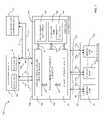
- FIG. 1depicts a block diagram of an exemplary processor-memory unit (PMU) for inclusion in a SiP or SiM device, in accordance with various embodiments of the present invention
- PMUprocessor-memory unit
- FIG. 2depicts a block diagram of a system module of the apparatus of FIG. 1 , in accordance with various embodiments of the invention.
- FIG. 3depicts a flow diagram illustrating a method for using the apparatus of FIG. 1 , in accordance with various embodiments of the present invention.
- Various embodiments of the inventiongenerally relate to a processor-memory unit for inclusion in a SIP or SiM device.
- the processor-memory unitincludes a system module configured to facilitate system integration and/or testing of different types of modules and component functional devices (e.g., different types of processors, ASICs, and/or memories) within the processor-memory unit.
- Some embodiments of the inventionmay be advantageously utilized in consumer products, such as digital cameras, gaming devices, media players, and the like. It will be appreciated by those skilled in the art that the invention may also be equally efficiently utilized within the context of other computerized products and devices.
- FIG. 1depicts a block diagram of an exemplary processor-memory unit (PMU) 100 for inclusion in a SiP or SiM device in accordance with various embodiments of the present invention.
- PMUprocessor-memory unit
- FIG. 1depicts a block diagram of an exemplary processor-memory unit (PMU) 100 for inclusion in a SiP or SiM device in accordance with various embodiments of the present invention.
- PMUprocessor-memory unit
- the PMU 100comprises a processing module 110 , a system module 120 encompassing programmable processor/ASIC-memory interfacing capabilities, and a memory module 130 .
- the processing module 110is coupled to the system module 120
- the system module 120is coupled to the memory module 130 using data/command buses 111 and 121 , respectively.
- system module 120acts as an interface between processing module 110 and memory module 130 .
- the modules of the PMU 100as well as their functional components, may be embodied in either separate dies within one or more IC (integrated circuit) packages or separately packaged IC devices.
- the processing module 110includes at least one processor (processors 112 and 114 are illustratively shown) and/or at least one logic ASIC (not shown), which optionally use the same bus 111 and optionally have the same or similar interfacing requirements for communicating to memory devices.
- the memory module 130may consist of at least one memory bank 132 (memory banks 132 1 - 132 N are shown, where N is an integer and N ⁇ 1). Because system module 120 is used as an interface between memory module 130 and processing module, each of the memory banks 132 may utilize a different data exchange protocol (e.g., read/write protocol) and different clock signals, and use command and data interfaces 136 and 138 having different widths.
- the memory module 130may comprise the memory banks 132 having different types of the memory cells.
- the memory module 130may comprise the memory banks 132 each having different types of the memory cells.
- the memory banks 132may comprise arrays of dynamic random access memory (DRAM) cells, static random access memory (SRAM) cells, FLASH memory cells, reduced latency DRAM (RLDRAM) cells, fast-cycle DRAM (FCDRAM) cells, RambusTM DRAM (RDRAM) cells, and/or double data rate DRAM (DDR DRAM) cells, among other types of memory cells.
- DRAMdynamic random access memory
- SRAMstatic random access memory
- FLASH memory cellsFLASH memory cells
- reduced latency DRAM (RLDRAM) cellsreduced latency DRAM (RLDRAM) cells
- FCDRAMfast-cycle DRAM
- RDRAMRambusTM DRAM
- DDR DRAMdouble data rate DRAM
- bus 111includes, for the purpose of example, a command interface 102 , a data interface 104 , a test data interface 106 and a test command interface 108 .
- the system module 120may be configured to be compatible with an optional external automatic test equipment ATE 150 .
- system module 120is configured such that the interfaces 106 and 108 are coupled to, and are pin-compatible with, respectively, interfaces 152 and 154 of external automatic test equipment (ATE) 150 .
- interface 152is configured for communicating test data
- interface 154is configured for communicating test commands.
- ATE 150may be used, without additional interfacing means, for post-assembly testing and monitoring performance and/or data exchanges between the modules 110 , 120 and 130 and/or their functional components.
- ATE 150is optionally an unmodified prior art test equipment device.
- the system module 120comprises a processor/ASIC and ATE interface (PAI) module 122 , a programmable data/command converter 124 , a memory interface module (MIM) 126 , and an optional controller 140 .
- the module 122is coupled to the converter 124 and the converter 124 is coupled to the MIM 126 using interfaces 162 and 164 , respectively.
- the controller 140is, typically, selectively coupled to the modules 122 , 124 , and 126 , for example by a means of interfaces 166 - 168 .
- SiPLINKTMProgrammable data/command converters under the trade name SiPLINKTM are available from Inapac Technology, Inc. of San Jose, Calif. Salient features of the converter adapted for use in the PMU 100 are discussed herein, for example in reference to FIG. 2 .
- the controller 140comprises a programmable logic circuit 142 and a memory bank 144 of, optionally non-volatile (NV), memory cells.
- a portion 146 of the memory bank 144is allocated for storing one or more programs executing internal test routines and performance monitoring routines in the PMU 100 , as well as for storing pre-programmed configuration settings for the system module 120 .
- the remaining portion (not shown) of the memory bank 144comprises one or more redundant memory cells, which are optionally used for replacing defective (e.g., failed) cells in the memory banks 132 .
- the processing module 110does not comprise logic ASICs, or the PMU 100 does not execute an internal test mode (as discussed elsewhere herein) or facilitate memory repairs, the controller 140 is optional.
- system module 120facilitates an operating mode and at least one of external test, monitoring, or internal test modes of the PMU 100 .
- the system module 120captures data/command streams from the processing module 110 , converts the captured streams to a communication protocol compatible with a protocol of an addressed memory bank 132 , and transmits the converted data/command streams from the processing module 110 to the memory banks 132 .
- the system module 120captures data/command streams from memory bank 132 , converts the captured streams to a communication protocol compatible with a protocol of the processing module 110 , and delivers the converted data streams to the processing module 110 .
- the system module 120stores converted data/command streams and schedules delivery of the streams in a manner maximizing efficiency of communications in the PMU 100 .
- the ATE 150executes test procedures and provides active real-time testing of signal flow and/or performance of the processing module 110 and memory banks 132 , among other functional components of the PMU 100 .
- the ATE 150passively monitors the data/command streams described, for example, in reference to the operating mode for analysis of malfunctioning and/or communication errors in the PMU 100 .
- some defects in the memory banks 132may be “repaired.”
- redundant NV memory cells of the memory bank 144are substituted for defective memory cells within memory module 130 .
- memory interface module 126is programmed to reroute memory fetches from the defective memory cells to the NV memory cells of the memory bank. This rerouting is transparent to processing module 110 .
- At least a portion of the functions described herein, in reference to the external test and monitoring modes,may be performed in-situ, by executing the test routines stored in the controller 140 .
- FIG. 2depicts a block diagram of system module 120 of the apparatus of FIG. 1 .
- the module 122comprises a command capture circuit 210 , a data capture & send circuit 212 , and a test input/output (I/O) circuit 214 .
- the converter 124comprises a clock signal(s) generator 220 configured for supplying a clock signal to the memory banks 132 , a data read/write configuration and scheduling (DRWCS) module 222 , a test controller 224 , a test mode logic circuit 226 , and a test data buffer 228 .
- the MIM 126comprises a plurality of N memory interface circuits (MICs) 230 (circuits 230 1 - 230 N are shown).
- an instance of MIC circuit 230includes an optional delay locked loop (DLL) 232 (DLLs 232 1 - 232 N are shown).
- DLLdelay locked loop
- a clock manager 250is configured to provide clock signals to clock signal(s) generator 220 , command capture circuit 210 and/or data capture & send circuit 212 , via data interfaces 254 and 260 .
- Clock manager 250optionally includes a phase-locked-loop and may be configured to buffer and manage clock signals received from external devices.
- clock manager 250is configured to receive a CK-IN signal 256 from a crystal oscillator or other device.
- clock manager 250is configured to receive an optional CLK input 252 from devices external to system module 120 .
- These devicesmay include processor 112 , processing module 110 , automatic test equipment (ATE) 150 , a phase-locked-loop, a clock synthesizer, or the like.
- clock manager 250receives clock signals from more than one source
- elements of system module 120 , memory module 130 and/or processing module 110may each operate at different clock frequencies.
- processing module 110may operate at a first clock frequency while system module 120 and/or memory module 130 operate at a different clock frequency.
- a clock signal received by clock manager 250is reduced (e.g., divided by 1.5, 2, 3 or 4 etc.) to produce an additional clock signal at a different frequency.
- elements of system module 120 and/or memory module 130may operated at different frequencies than elements of processing module 110 or automatic test equipment (ATE) 150 .
- Signal flow between respective components of the modules 122 , 124 and 140is selectively provided by command interfaces 216 , 217 , 221 , 223 , 227 , and 229 and data interfaces 213 , 215 , 218 , and 225 . Accordingly, the signal flow between the PAI module 124 and memory interface circuits 230 is facilitated using data/command buses 241 - 246 coupled via a data/command system bus 240 . Collectively, these buses and interfaces form the buses 162 , 164 , and 166 - 168 discussed above in reference to FIG. 1 .
- the generator 220uses at least one of clock signals of a processor or logic ASIC of the processing module 110 as a base signal(s) to form one or more clock signals for the memory banks 132 .
- configuration/scheduling settings for the DRWCS module 222may be provided by the processing module 110 via a path comprising the data interfaces 104 , 213 and the data capture & send circuit 212 and initiated by a command communicated via a path comprising the command interfaces 102 , 217 and the command capture circuit 210 .
- the controller 140may be used to program the DRWCS module 222 via the data and command links coupled to, e.g., the interfaces 213 and 217 , respectively.
- the ATE 150 or other external programming devicee.g., computer
- the DRWCS module 222matches data exchange protocols used by components of the processing module 110 (e.g., processor 112 or 114 ) and the addressed memory bank 132 , temporarily stores the converted data and/or commands (e.g., in an internal buffer (not shown)), and transmits the stored data and commands to the intended addressees.
- the DRWCS module 222selectively converts outgoing signals of the processing module 110 in one on more protocols compatible with the respective memory banks 132 and converts the outgoing signals from the memory banks 132 into the protocols compatible with the addressed processor or logic ASIC of the processing module 110 .
- the DRWCS module 222provides scheduling (or grouping) of the stored information before transmitting to the respective destination.
- data and commands from the processing module 110(via a path comprising the data interfaces 104 , 213 and the data capture & send circuit 212 and a path comprising command interfaces 102 , 217 and the command capture circuit 210 , respectively) in a memory-compatible format are placed, via a bus 242 , on the system bus 240 .
- configuration settings for the data capture circuit 212may be provided, via the interface 216 , by the processing module 110 . From the system bus 240 , such data and commands become available to the MICs 230 each selectively coupled to the respective memory bank 132 .
- test data and test commands from the ATE 150are placed, via a bus 243 , on the system bus 240 and become available to the MICs 230 and memory banks 132 , as well as to the processing module 110 .
- These test commandsmay be communicated via a path comprising the data interfaces 106 / 152 , 215 and the test I/O circuit 214 and test data buffer 228 , and a path comprising command interfaces 108 / 154 , 221 , 229 and the test controller 224 and test mode logic circuit 226 , respectively.
- the ATE 150 and processing module 110may control configuration settings of the programmable logic circuit 142 , via the interfaces 108 / 154 , the test controller 224 , and interfaces 221 and 223 .
- the ATE 150may monitor data/command exchanges in the system module 120 . These exchanges are optionally made via the bus 243 , the test data buffer 228 , the test I/O circuit 214 , and the data interface 106 / 152 .
- test data and test commands provided or monitored by the ATE 150 in the external test and monitoring modesmay be similarly provided or monitored, via the interfaces 225 and 227 , using the controller 140 .
- FIG. 3depicts a flow diagram illustrating a method 300 in accordance with various embodiments.
- the method 300includes processing steps performed for assembling and testing the PMU 100 (e.g., steps 310 - 340 ), as well as steps for using the PMU 100 (e.g., steps 350 - 370 ).
- the assembly and use of PMU 100are optionally performed as separate methods.
- the illustrated stepsare sequentially performed in the depicted order. In alternate embodiments, some of the steps may be performed contemporaneously or in a different order. To best understand the invention, the reader should simultaneously refer to FIGS. 1-3 .
- the method 300starts at step 302 and proceeds to step 310 .
- the processing module 110 , system module 120 , and memory module 130 of the PMU 100are provided and received for assembly.
- the processing module 110 , system module 120 , and memory module 130may be received for inclusion in SiP or SiM devices.
- step 320data, command, and test interfaces are facilitated between the processing module 110 , system module 120 , and ATE 150 .
- This facilitationmay include construction of electrical interconnects, command interfaces, data busses, signal channels, soldering of bond pads, or the like.
- the system module 120encompasses programmable processor/ASIC-memory interfacing capabilities and shares the same pin-compatible test interfaces 106 / 152 (data) and 108 / 154 (commands) with the processing module 110 and external ATE 150 .
- step 330data, command, and test interfaces are facilitated between the system module 110 and memory module 130 .
- This facilitationmay include construction of electrical interconnects, command interfaces, data busses, signal channels, soldering of bond pads, or the like.
- the facilitation of steps 320 and 330can also include packaging of the components, providing signals to the interfaces, or the like.
- the system module 120is programmed to provide signal/protocol compatibility between the processing module 110 and the memory banks 132 of the memory module 130 , as well as, optionally, for providing external (ATE 150 ) and/or internal (controller 140 ) testability of the PMU 100 .
- Configuration settings for use in programmingmay be provided to the system module using the processing module 110 , ATE 150 , or external programming device.
- the system module 120is used to perform data and/or command communications between the processing module 110 and memory module 130 by converting the incoming and outgoing data/command streams into formats compatible with the protocols and requirements of the respective recipients of these streams, as discussed above in reference to the operating mode of the PMU 100 .
- the DRWCS module 222is used to schedule transmission of outgoing data/command streams to their respective destinations.
- step 360functional components of the memory module 130 and processing module 110 , as well as portions of the system module 120 , are tested/monitored using the ATE 150 or controller 140 , as discussed above in the context of the external test, monitoring, and internal test modes of the PMU 100 .
- step 370upon completion of step 360 , the method 300 ends.
Landscapes
- Tests Of Electronic Circuits (AREA)
Abstract
Description
Claims (31)
Priority Applications (4)
| Application Number | Priority Date | Filing Date | Title |
|---|---|---|---|
| US11/208,099US7673193B1 (en) | 2005-08-18 | 2005-08-18 | Processor-memory unit for use in system-in-package and system-in-module devices |
| US11/472,016US7466160B2 (en) | 2002-11-27 | 2006-06-20 | Shared memory bus architecture for system with processor and memory units |
| US12/646,540US7945824B2 (en) | 2005-08-18 | 2009-12-23 | Processor-memory unit for use in system-in-package and system-in-module devices |
| US13/093,720US8195992B2 (en) | 2005-08-18 | 2011-04-25 | Processor-memory unit for use in system-in-package and system-in-module devices |
Applications Claiming Priority (1)
| Application Number | Priority Date | Filing Date | Title |
|---|---|---|---|
| US11/208,099US7673193B1 (en) | 2005-08-18 | 2005-08-18 | Processor-memory unit for use in system-in-package and system-in-module devices |
Related Parent Applications (1)
| Application Number | Title | Priority Date | Filing Date |
|---|---|---|---|
| US10/679,673Continuation-In-PartUS7006940B1 (en) | 2000-09-21 | 2003-10-03 | Set up for a first integrated circuit chip to allow for testing of a co-packaged second integrated circuit chip |
Related Child Applications (3)
| Application Number | Title | Priority Date | Filing Date |
|---|---|---|---|
| US11/223,286Continuation-In-PartUS7245141B2 (en) | 2001-09-28 | 2005-09-09 | Shared bond pad for testing a memory within a packaged semiconductor device |
| US11/472,016Continuation-In-PartUS7466160B2 (en) | 2002-11-27 | 2006-06-20 | Shared memory bus architecture for system with processor and memory units |
| US12/646,540ContinuationUS7945824B2 (en) | 2005-08-18 | 2009-12-23 | Processor-memory unit for use in system-in-package and system-in-module devices |
Publications (1)
| Publication Number | Publication Date |
|---|---|
| US7673193B1true US7673193B1 (en) | 2010-03-02 |
Family
ID=41717750
Family Applications (3)
| Application Number | Title | Priority Date | Filing Date |
|---|---|---|---|
| US11/208,099Active2028-12-29US7673193B1 (en) | 2002-11-27 | 2005-08-18 | Processor-memory unit for use in system-in-package and system-in-module devices |
| US12/646,540Expired - LifetimeUS7945824B2 (en) | 2005-08-18 | 2009-12-23 | Processor-memory unit for use in system-in-package and system-in-module devices |
| US13/093,720Expired - LifetimeUS8195992B2 (en) | 2005-08-18 | 2011-04-25 | Processor-memory unit for use in system-in-package and system-in-module devices |
Family Applications After (2)
| Application Number | Title | Priority Date | Filing Date |
|---|---|---|---|
| US12/646,540Expired - LifetimeUS7945824B2 (en) | 2005-08-18 | 2009-12-23 | Processor-memory unit for use in system-in-package and system-in-module devices |
| US13/093,720Expired - LifetimeUS8195992B2 (en) | 2005-08-18 | 2011-04-25 | Processor-memory unit for use in system-in-package and system-in-module devices |
Country Status (1)
| Country | Link |
|---|---|
| US (3) | US7673193B1 (en) |
Cited By (14)
| Publication number | Priority date | Publication date | Assignee | Title |
|---|---|---|---|---|
| US20070067687A1 (en)* | 2001-09-28 | 2007-03-22 | Ong Adrian E | Integrated Circuit Testing Module Configured for Set-up and Hold Time Testing |
| US20070079204A1 (en)* | 2001-09-28 | 2007-04-05 | Ong Adrian E | Integrated Circuit Testing Module Including Signal Shaping Interface |
| US20100228514A1 (en)* | 2006-06-30 | 2010-09-09 | Rambus Inc. | Delay lock loop delay adjusting method and apparatus |
| US8063650B2 (en) | 2002-11-27 | 2011-11-22 | Rambus Inc. | Testing fuse configurations in semiconductor devices |
| US8286046B2 (en) | 2001-09-28 | 2012-10-09 | Rambus Inc. | Integrated circuit testing module including signal shaping interface |
| DE102013112900A1 (en) | 2012-11-30 | 2014-06-05 | Samsung Electronics Co., Ltd. | Method and system for providing an intelligent memory architecture |
| US9069719B2 (en) | 2012-02-11 | 2015-06-30 | Samsung Electronics Co., Ltd. | Method and system for providing a smart memory architecture |
| US20150332787A1 (en)* | 2014-05-13 | 2015-11-19 | SK Hynix Inc. | Semiconductor memory apparatus |
| TWI602278B (en)* | 2015-11-05 | 2017-10-11 | 凌陽科技股份有限公司 | Semiconductor apparatus |
| US10049763B2 (en) | 2014-05-13 | 2018-08-14 | SK Hynix Inc. | Semiconductor memory apparatus |
| US10679711B2 (en) | 2018-03-22 | 2020-06-09 | Toshiba Memory Corporation | Memory system including power supply control circuit and temperature sensor, and control method thereof |
| US11314278B2 (en)* | 2016-01-25 | 2022-04-26 | Samsung Electronics Co., Ltd. | Semiconductor device, semiconductor system and method for operating semiconductor device |
| US11340685B2 (en) | 2016-01-25 | 2022-05-24 | Samsung Electronics Co., Ltd. | Semiconductor device including clock management unit for outputting clock and acknowledgment signals to an intelectual property block |
| US20230314499A1 (en)* | 2022-03-31 | 2023-10-05 | Advantest Test Solutions, Inc. | Test system support component exchange system and method |
Families Citing this family (2)
| Publication number | Priority date | Publication date | Assignee | Title |
|---|---|---|---|---|
| US8966457B2 (en)* | 2011-11-15 | 2015-02-24 | Global Supercomputing Corporation | Method and system for converting a single-threaded software program into an application-specific supercomputer |
| US10572427B2 (en) | 2017-11-13 | 2020-02-25 | Data I/O Corporation | Device programming system with protocol emulation |
Citations (33)
| Publication number | Priority date | Publication date | Assignee | Title |
|---|---|---|---|---|
| US5594694A (en) | 1995-07-28 | 1997-01-14 | Micron Quantum Devices, Inc. | Memory circuit with switch for selectively connecting an input/output pad directly to a nonvolatile memory cell |
| US5825697A (en) | 1995-12-22 | 1998-10-20 | Micron Technology, Inc. | Circuit and method for enabling a function in a multiple memory device module |
| US6191603B1 (en) | 1999-01-08 | 2001-02-20 | Agilent Technologies Inc. | Modular embedded test system for use in integrated circuits |
| US6365421B2 (en) | 1996-06-13 | 2002-04-02 | Micron Technology, Inc. | Method and apparatus for storage of test results within an integrated circuit |
| US6457141B1 (en) | 1998-10-08 | 2002-09-24 | Samsung Electronics Co., Ltd. | Semiconductor device with embedded memory cells |
| US20020178416A1 (en)* | 2001-05-23 | 2002-11-28 | Ibm Corporation | Hierarchical built-in self-test for system-on-chip design |
| US6492727B2 (en) | 2000-03-03 | 2002-12-10 | Hitachi, Ltd. | Semiconductor device |
| US6519171B2 (en) | 2000-11-17 | 2003-02-11 | Fujitsu Limited | Semiconductor device and multichip module |
| US6531339B2 (en) | 1998-12-23 | 2003-03-11 | Micron Technology, Inc. | Redundancy mapping in a multichip semiconductor package |
| US20030120985A1 (en)* | 2001-12-26 | 2003-06-26 | Richard Slobodnik | Method and apparatus for memory self testing |
| US6711042B2 (en)* | 2001-09-05 | 2004-03-23 | Fujitsu Limited | Semiconductor device whereon memory chip and logic chip are mounted, making testing of memory chip possible |
| US6732304B1 (en)* | 2000-09-21 | 2004-05-04 | Inapac Technology, Inc. | Chip testing within a multi-chip semiconductor package |
| US20040100296A1 (en) | 2002-11-27 | 2004-05-27 | Ong Adrian E. | Bonding pads for testing of a semiconductor device |
| US6825683B1 (en) | 2002-04-18 | 2004-11-30 | Cypress Semiconductor Corporation | System and method for testing multiple integrated circuits that are in the same package |
| US20050024977A1 (en) | 2000-09-21 | 2005-02-03 | Ong Adrian E. | Multiple power levels for a chip within a multi-chip semiconductor package |
| US6967397B2 (en) | 2000-10-20 | 2005-11-22 | Oki Electric Industry Co., Ltd. | Test circuit and multi-chip package type semiconductor device having the test circuit |
| US6973405B1 (en)* | 2002-05-22 | 2005-12-06 | Xilinx, Inc. | Programmable interactive verification agent |
| US20050289428A1 (en) | 2000-09-21 | 2005-12-29 | Sidley Austin Brown & Wood Llp | Architecture and method for testing of an integrated circuit device |
| US6996745B1 (en) | 2001-09-27 | 2006-02-07 | Sun Microsystems, Inc. | Process for shutting down a CPU in a SMP configuration |
| US7006940B1 (en) | 2002-11-27 | 2006-02-28 | Inapac Technology, Inc. | Set up for a first integrated circuit chip to allow for testing of a co-packaged second integrated circuit chip |
| US7053470B1 (en) | 2005-02-19 | 2006-05-30 | Azul Systems, Inc. | Multi-chip package having repairable embedded memories on a system chip with an EEPROM chip storing repair information |
| US7061263B1 (en) | 2001-11-15 | 2006-06-13 | Inapac Technology, Inc. | Layout and use of bond pads and probe pads for testing of integrated circuits devices |
| US7075175B2 (en) | 2004-04-22 | 2006-07-11 | Qualcomm Incorporated | Systems and methods for testing packaged dies |
| US20060152241A1 (en) | 2002-11-27 | 2006-07-13 | Inapac Technology, Inc. | Shared bond pad for testing a memory within a packaged semiconductor device |
| US7133798B1 (en) | 2004-10-18 | 2006-11-07 | Inapac Technology, Inc. | Monitoring signals between two integrated circuit devices within a single package |
| US7149135B2 (en) | 2003-10-30 | 2006-12-12 | Kabushiki Kaisha Toshiba | Multi chip package type memory system and a replacement method of replacing a defect therein |
| US7249301B2 (en)* | 2003-07-30 | 2007-07-24 | Infineon Technologies Ag | Semiconductor circuit and method for testing, monitoring and application-near setting of a semiconductor circuit |
| US7269765B1 (en) | 2000-04-13 | 2007-09-11 | Micron Technology, Inc. | Method and apparatus for storing failing part locations in a module |
| US7305595B2 (en) | 2003-09-11 | 2007-12-04 | International Business Machines Corporation | Method, system, and product for isolating memory system defects to a particular memory system component |
| US7353442B2 (en)* | 2004-04-08 | 2008-04-01 | Stmicroelectronics Pvt. Ltd. | On-chip and at-speed tester for testing and characterization of different types of memories |
| US20080133206A1 (en)* | 2002-02-01 | 2008-06-05 | Devins Robert J | Method of switching external models in an automated system-on-chip integrated circuit design verification system |
| US20080313583A1 (en)* | 2005-07-14 | 2008-12-18 | International Business Machines Corporation | Apparatus and Method for Testing Sub-Systems of a System-on-a-Chip Using a Configurable External System-on-a-Chip |
| US7484188B2 (en)* | 2006-03-15 | 2009-01-27 | Marvell International Technology Ltd. | On-chip test circuit and method for testing of system-on-chip (SOC) integrated circuits |
Family Cites Families (18)
| Publication number | Priority date | Publication date | Assignee | Title |
|---|---|---|---|---|
| US5850513A (en)* | 1996-01-05 | 1998-12-15 | Unisys Corporation | Processor path emulation system providing fast readout and verification of main memory by maintenance controller interface to maintenance subsystem |
| US6865663B2 (en)* | 2000-02-24 | 2005-03-08 | Pts Corporation | Control processor dynamically loading shadow instruction register associated with memory entry of coprocessor in flexible coupling mode |
| JP2001337845A (en)* | 2000-05-30 | 2001-12-07 | Mitsubishi Electric Corp | Microprocessor |
| US20020105522A1 (en)* | 2000-12-12 | 2002-08-08 | Kolluru Mahadev S. | Embedded memory architecture for video applications |
| US7365557B1 (en)* | 2001-09-28 | 2008-04-29 | Inapac Technology, Inc. | Integrated circuit testing module including data generator |
| US7265570B2 (en)* | 2001-09-28 | 2007-09-04 | Inapac Technology, Inc. | Integrated circuit testing module |
| US8166361B2 (en)* | 2001-09-28 | 2012-04-24 | Rambus Inc. | Integrated circuit testing module configured for set-up and hold time testing |
| US20040019841A1 (en)* | 2002-07-25 | 2004-01-29 | Ong Adrian E. | Internally generating patterns for testing in an integrated circuit device |
| US7313740B2 (en)* | 2002-07-25 | 2007-12-25 | Inapac Technology, Inc. | Internally generating patterns for testing in an integrated circuit device |
| US7446551B1 (en)* | 2001-09-28 | 2008-11-04 | Inapac Technology, Inc. | Integrated circuit testing module including address generator |
| US7404117B2 (en)* | 2005-10-24 | 2008-07-22 | Inapac Technology, Inc. | Component testing and recovery |
| US7370256B2 (en)* | 2001-09-28 | 2008-05-06 | Inapac Technology, Inc. | Integrated circuit testing module including data compression |
| US7309999B2 (en)* | 2002-11-27 | 2007-12-18 | Inapac Technology, Inc. | Electronic device having an interface supported testing mode |
| US7466160B2 (en)* | 2002-11-27 | 2008-12-16 | Inapac Technology, Inc. | Shared memory bus architecture for system with processor and memory units |
| US7325178B2 (en)* | 2003-12-05 | 2008-01-29 | Texas Instruments Incorporated | Programmable built in self test of memory |
| US7360130B2 (en)* | 2004-05-24 | 2008-04-15 | Jed Margolin | Memory with integrated programmable controller |
| US7779311B2 (en)* | 2005-10-24 | 2010-08-17 | Rambus Inc. | Testing and recovery in a multilayer device |
| US7269524B1 (en)* | 2006-06-30 | 2007-09-11 | Inapac Technology, Inc. | Delay lock loop delay adjusting method and apparatus |
- 2005
- 2005-08-18USUS11/208,099patent/US7673193B1/enactiveActive
- 2009
- 2009-12-23USUS12/646,540patent/US7945824B2/ennot_activeExpired - Lifetime
- 2011
- 2011-04-25USUS13/093,720patent/US8195992B2/ennot_activeExpired - Lifetime
Patent Citations (38)
| Publication number | Priority date | Publication date | Assignee | Title |
|---|---|---|---|---|
| US5594694A (en) | 1995-07-28 | 1997-01-14 | Micron Quantum Devices, Inc. | Memory circuit with switch for selectively connecting an input/output pad directly to a nonvolatile memory cell |
| US5825697A (en) | 1995-12-22 | 1998-10-20 | Micron Technology, Inc. | Circuit and method for enabling a function in a multiple memory device module |
| US6365421B2 (en) | 1996-06-13 | 2002-04-02 | Micron Technology, Inc. | Method and apparatus for storage of test results within an integrated circuit |
| US6457141B1 (en) | 1998-10-08 | 2002-09-24 | Samsung Electronics Co., Ltd. | Semiconductor device with embedded memory cells |
| US6531339B2 (en) | 1998-12-23 | 2003-03-11 | Micron Technology, Inc. | Redundancy mapping in a multichip semiconductor package |
| US6191603B1 (en) | 1999-01-08 | 2001-02-20 | Agilent Technologies Inc. | Modular embedded test system for use in integrated circuits |
| US6492727B2 (en) | 2000-03-03 | 2002-12-10 | Hitachi, Ltd. | Semiconductor device |
| US7269765B1 (en) | 2000-04-13 | 2007-09-11 | Micron Technology, Inc. | Method and apparatus for storing failing part locations in a module |
| US20050024977A1 (en) | 2000-09-21 | 2005-02-03 | Ong Adrian E. | Multiple power levels for a chip within a multi-chip semiconductor package |
| US20050289428A1 (en) | 2000-09-21 | 2005-12-29 | Sidley Austin Brown & Wood Llp | Architecture and method for testing of an integrated circuit device |
| US6732304B1 (en)* | 2000-09-21 | 2004-05-04 | Inapac Technology, Inc. | Chip testing within a multi-chip semiconductor package |
| US20040196709A1 (en) | 2000-09-21 | 2004-10-07 | Ong Adrian E. | Chip testing within a multi-chip semiconductor package |
| US7139945B2 (en) | 2000-09-21 | 2006-11-21 | Inapac Technology, Inc. | Chip testing within a multi-chip semiconductor package |
| US6967397B2 (en) | 2000-10-20 | 2005-11-22 | Oki Electric Industry Co., Ltd. | Test circuit and multi-chip package type semiconductor device having the test circuit |
| US6519171B2 (en) | 2000-11-17 | 2003-02-11 | Fujitsu Limited | Semiconductor device and multichip module |
| US20020178416A1 (en)* | 2001-05-23 | 2002-11-28 | Ibm Corporation | Hierarchical built-in self-test for system-on-chip design |
| US6711042B2 (en)* | 2001-09-05 | 2004-03-23 | Fujitsu Limited | Semiconductor device whereon memory chip and logic chip are mounted, making testing of memory chip possible |
| US6996745B1 (en) | 2001-09-27 | 2006-02-07 | Sun Microsystems, Inc. | Process for shutting down a CPU in a SMP configuration |
| US7061263B1 (en) | 2001-11-15 | 2006-06-13 | Inapac Technology, Inc. | Layout and use of bond pads and probe pads for testing of integrated circuits devices |
| US20030120985A1 (en)* | 2001-12-26 | 2003-06-26 | Richard Slobodnik | Method and apparatus for memory self testing |
| US20080133206A1 (en)* | 2002-02-01 | 2008-06-05 | Devins Robert J | Method of switching external models in an automated system-on-chip integrated circuit design verification system |
| US6825683B1 (en) | 2002-04-18 | 2004-11-30 | Cypress Semiconductor Corporation | System and method for testing multiple integrated circuits that are in the same package |
| US6973405B1 (en)* | 2002-05-22 | 2005-12-06 | Xilinx, Inc. | Programmable interactive verification agent |
| US20050204223A1 (en) | 2002-11-27 | 2005-09-15 | Ong Adrian E. | Bonding pads for testing of a semiconductor device |
| US7006940B1 (en) | 2002-11-27 | 2006-02-28 | Inapac Technology, Inc. | Set up for a first integrated circuit chip to allow for testing of a co-packaged second integrated circuit chip |
| US20040100296A1 (en) | 2002-11-27 | 2004-05-27 | Ong Adrian E. | Bonding pads for testing of a semiconductor device |
| US20060152241A1 (en) | 2002-11-27 | 2006-07-13 | Inapac Technology, Inc. | Shared bond pad for testing a memory within a packaged semiconductor device |
| US6812726B1 (en) | 2002-11-27 | 2004-11-02 | Inapac Technology, Inc. | Entering test mode and accessing of a packaged semiconductor device |
| US6882171B2 (en) | 2002-11-27 | 2005-04-19 | Inapac Technology, Inc. | Bonding pads for testing of a semiconductor device |
| US7249301B2 (en)* | 2003-07-30 | 2007-07-24 | Infineon Technologies Ag | Semiconductor circuit and method for testing, monitoring and application-near setting of a semiconductor circuit |
| US7305595B2 (en) | 2003-09-11 | 2007-12-04 | International Business Machines Corporation | Method, system, and product for isolating memory system defects to a particular memory system component |
| US7149135B2 (en) | 2003-10-30 | 2006-12-12 | Kabushiki Kaisha Toshiba | Multi chip package type memory system and a replacement method of replacing a defect therein |
| US7353442B2 (en)* | 2004-04-08 | 2008-04-01 | Stmicroelectronics Pvt. Ltd. | On-chip and at-speed tester for testing and characterization of different types of memories |
| US7075175B2 (en) | 2004-04-22 | 2006-07-11 | Qualcomm Incorporated | Systems and methods for testing packaged dies |
| US7133798B1 (en) | 2004-10-18 | 2006-11-07 | Inapac Technology, Inc. | Monitoring signals between two integrated circuit devices within a single package |
| US7053470B1 (en) | 2005-02-19 | 2006-05-30 | Azul Systems, Inc. | Multi-chip package having repairable embedded memories on a system chip with an EEPROM chip storing repair information |
| US20080313583A1 (en)* | 2005-07-14 | 2008-12-18 | International Business Machines Corporation | Apparatus and Method for Testing Sub-Systems of a System-on-a-Chip Using a Configurable External System-on-a-Chip |
| US7484188B2 (en)* | 2006-03-15 | 2009-01-27 | Marvell International Technology Ltd. | On-chip test circuit and method for testing of system-on-chip (SOC) integrated circuits |
Cited By (28)
| Publication number | Priority date | Publication date | Assignee | Title |
|---|---|---|---|---|
| US8286046B2 (en) | 2001-09-28 | 2012-10-09 | Rambus Inc. | Integrated circuit testing module including signal shaping interface |
| US20070079204A1 (en)* | 2001-09-28 | 2007-04-05 | Ong Adrian E | Integrated Circuit Testing Module Including Signal Shaping Interface |
| US10114073B2 (en) | 2001-09-28 | 2018-10-30 | Rambus Inc. | Integrated circuit testing |
| US20070067687A1 (en)* | 2001-09-28 | 2007-03-22 | Ong Adrian E | Integrated Circuit Testing Module Configured for Set-up and Hold Time Testing |
| US8001439B2 (en) | 2001-09-28 | 2011-08-16 | Rambus Inc. | Integrated circuit testing module including signal shaping interface |
| US9116210B2 (en) | 2001-09-28 | 2015-08-25 | Rambus Inc. | Integrated circuit testing module including signal shaping interface |
| US8166361B2 (en) | 2001-09-28 | 2012-04-24 | Rambus Inc. | Integrated circuit testing module configured for set-up and hold time testing |
| US9568544B2 (en) | 2002-11-27 | 2017-02-14 | Rambus Inc. | Testing fuse configurations in semiconductor devices |
| US8063650B2 (en) | 2002-11-27 | 2011-11-22 | Rambus Inc. | Testing fuse configurations in semiconductor devices |
| US11009548B2 (en) | 2002-11-27 | 2021-05-18 | Rambus Inc. | Testing fuse configurations in semiconductor devices |
| US8717052B2 (en) | 2002-11-27 | 2014-05-06 | Rambus Inc. | Testing fuse configurations in semiconductor devices |
| US10302696B2 (en) | 2002-11-27 | 2019-05-28 | Rambus Inc. | Testing fuse configurations in semiconductor devices |
| US20100228514A1 (en)* | 2006-06-30 | 2010-09-09 | Rambus Inc. | Delay lock loop delay adjusting method and apparatus |
| US7991572B2 (en) | 2006-06-30 | 2011-08-02 | Rambus Inc. | Delay lock loop delay adjusting method and apparatus |
| US9069719B2 (en) | 2012-02-11 | 2015-06-30 | Samsung Electronics Co., Ltd. | Method and system for providing a smart memory architecture |
| US9679664B2 (en) | 2012-02-11 | 2017-06-13 | Samsung Electronics Co., Ltd. | Method and system for providing a smart memory architecture |
| DE102013112900A1 (en) | 2012-11-30 | 2014-06-05 | Samsung Electronics Co., Ltd. | Method and system for providing an intelligent memory architecture |
| US9349488B2 (en)* | 2014-05-13 | 2016-05-24 | SK Hynix Inc. | Semiconductor memory apparatus |
| US10049763B2 (en) | 2014-05-13 | 2018-08-14 | SK Hynix Inc. | Semiconductor memory apparatus |
| US20150332787A1 (en)* | 2014-05-13 | 2015-11-19 | SK Hynix Inc. | Semiconductor memory apparatus |
| TWI602278B (en)* | 2015-11-05 | 2017-10-11 | 凌陽科技股份有限公司 | Semiconductor apparatus |
| US11314278B2 (en)* | 2016-01-25 | 2022-04-26 | Samsung Electronics Co., Ltd. | Semiconductor device, semiconductor system and method for operating semiconductor device |
| US11340685B2 (en) | 2016-01-25 | 2022-05-24 | Samsung Electronics Co., Ltd. | Semiconductor device including clock management unit for outputting clock and acknowledgment signals to an intelectual property block |
| US11747853B2 (en) | 2016-01-25 | 2023-09-05 | Samsung Electronics Co., Ltd. | Semiconductor device, semiconductor system and method for operating semiconductor device |
| US11789515B2 (en) | 2016-01-25 | 2023-10-17 | Samsung Electronics Co., Ltd. | Semiconductor device |
| US10679711B2 (en) | 2018-03-22 | 2020-06-09 | Toshiba Memory Corporation | Memory system including power supply control circuit and temperature sensor, and control method thereof |
| US20230314499A1 (en)* | 2022-03-31 | 2023-10-05 | Advantest Test Solutions, Inc. | Test system support component exchange system and method |
| US12235315B2 (en)* | 2022-03-31 | 2025-02-25 | Advantest Test Solutions, Inc. | Test system support component exchange system and method |
Also Published As
| Publication number | Publication date |
|---|---|
| US8195992B2 (en) | 2012-06-05 |
| US7945824B2 (en) | 2011-05-17 |
| US20110202789A1 (en) | 2011-08-18 |
| US20100100661A1 (en) | 2010-04-22 |
Similar Documents
| Publication | Publication Date | Title |
|---|---|---|
| US7945824B2 (en) | Processor-memory unit for use in system-in-package and system-in-module devices | |
| CN112703409B (en) | Automatic test equipment, method and computer program | |
| US9117685B2 (en) | Reconfiguring through silicon vias in stacked multi-die packages | |
| US7480830B2 (en) | System, method and storage medium for testing a memory module | |
| US12079098B2 (en) | Automated test equipment with hardware accelerator | |
| US20160163609A1 (en) | Methods and apparatus for testing auxiliary components in a multichip package | |
| KR20160019398A (en) | A tester with mixed protocol engine in a fpga block | |
| US8555122B2 (en) | Interface device and method | |
| US6181616B1 (en) | Circuits and systems for realigning data output by semiconductor testers to packet-based devices under test | |
| US20210074680A1 (en) | Through-silicon via (tsv) test circuit, tsv test method and integrated circuits (ic) chip | |
| CN113391142A (en) | Providing protocol flexibility in automated test equipment using host bus adapters | |
| US20140110711A1 (en) | Stacked chip module with integrated circuit chips having integratable built-in self-maintenance blocks | |
| Amory et al. | Wrapper design for the reuse of a bus, network-on-chip, or other functional interconnect as test access mechanism [Note 1] | |
| CN101599306B (en) | Field mounting-type test apparatus and method | |
| US9116876B2 (en) | Programmable built-in-self tester (BIST) in memory controller | |
| CN101167141A (en) | Test system for memory chip in MCP or SIP | |
| US6760871B2 (en) | Circuit, system and method for arranging data output by semiconductor testers to packet-based devices under test | |
| CN104952487B (en) | A method of operating a multi-chip packaging device | |
| US10541043B1 (en) | On demand data stream controller for programming and executing operations in an integrated circuit | |
| US7600168B2 (en) | Apparatus with programmable scan chains for multiple chip modules and method for programming the same | |
| US7353425B2 (en) | Data processing circuit apparatus having a data transmission unit of redundant design | |
| US6885961B2 (en) | Hybrid tester architecture | |
| CN116825170B (en) | Automatic calibration architecture and chip for die-to-die interconnect | |
| US7117410B2 (en) | Distributed failure analysis memory for automatic test equipment | |
| CN117271434B (en) | On-site programmable system-in-chip |
Legal Events
| Date | Code | Title | Description |
|---|---|---|---|
| AS | Assignment | Owner name:INAPAC TECHNOLOGY, INC.,CALIFORNIA Free format text:ASSIGNMENT OF ASSIGNORS INTEREST;ASSIGNORS:ONG, ADRIAN E.;BALIGA, NARESH;REEL/FRAME:016910/0103 Effective date:20050816 | |
| AS | Assignment | Owner name:CARR & FERRELL LLP,CALIFORNIA Free format text:UCC FINANCING STATEMENT FILED IN CALIFORNIA;ASSIGNOR:INAPAC TECHNOLOGY, INC.;REEL/FRAME:021425/0952 Effective date:20080811 Owner name:CARR & FERRELL LLP, CALIFORNIA Free format text:UCC FINANCING STATEMENT FILED IN CALIFORNIA;ASSIGNOR:INAPAC TECHNOLOGY, INC.;REEL/FRAME:021425/0952 Effective date:20080811 | |
| AS | Assignment | Owner name:INAPAC TECHNOLOGY, INC.,CALIFORNIA Free format text:RELEASE OF SECURITY AGREEMENT (CA);ASSIGNOR:CARR & FERRELL LLP;REEL/FRAME:022158/0338 Effective date:20090114 Owner name:INAPAC TECHNOLOGY, INC., CALIFORNIA Free format text:RELEASE OF SECURITY AGREEMENT (CA);ASSIGNOR:CARR & FERRELL LLP;REEL/FRAME:022158/0338 Effective date:20090114 | |
| AS | Assignment | Owner name:RAMBUS INC.,CALIFORNIA Free format text:ASSIGNMENT OF ASSIGNORS INTEREST;ASSIGNOR:INAPAC TECHNOLOGY, INC.;REEL/FRAME:022597/0896 Effective date:20090227 Owner name:RAMBUS INC., CALIFORNIA Free format text:ASSIGNMENT OF ASSIGNORS INTEREST;ASSIGNOR:INAPAC TECHNOLOGY, INC.;REEL/FRAME:022597/0896 Effective date:20090227 | |
| STCF | Information on status: patent grant | Free format text:PATENTED CASE | |
| FPAY | Fee payment | Year of fee payment:4 | |
| FEPP | Fee payment procedure | Free format text:PAYOR NUMBER ASSIGNED (ORIGINAL EVENT CODE: ASPN); ENTITY STATUS OF PATENT OWNER: LARGE ENTITY | |
| AS | Assignment | Owner name:SCA IPLA HOLDINGS INC., NEW YORK Free format text:ASSIGNMENT OF ASSIGNORS INTEREST;ASSIGNOR:RAMBUS INC.;REEL/FRAME:033026/0152 Effective date:20140401 | |
| MAFP | Maintenance fee payment | Free format text:PAYMENT OF MAINTENANCE FEE, 8TH YEAR, LARGE ENTITY (ORIGINAL EVENT CODE: M1552) Year of fee payment:8 | |
| MAFP | Maintenance fee payment | Free format text:PAYMENT OF MAINTENANCE FEE, 12TH YEAR, LARGE ENTITY (ORIGINAL EVENT CODE: M1553); ENTITY STATUS OF PATENT OWNER: LARGE ENTITY Year of fee payment:12 |