US7671620B2 - Testing system for solar cells - Google Patents
Testing system for solar cellsDownload PDFInfo
- Publication number
- US7671620B2 US7671620B2US11/249,298US24929805AUS7671620B2US 7671620 B2US7671620 B2US 7671620B2US 24929805 AUS24929805 AUS 24929805AUS 7671620 B2US7671620 B2US 7671620B2
- Authority
- US
- United States
- Prior art keywords
- solar cells
- electrical
- conveyor belt
- checking
- testing system
- Prior art date
- Legal status (The legal status is an assumption and is not a legal conclusion. Google has not performed a legal analysis and makes no representation as to the accuracy of the status listed.)
- Expired - Fee Related, expires
Links
Images


Classifications
- H—ELECTRICITY
- H02—GENERATION; CONVERSION OR DISTRIBUTION OF ELECTRIC POWER
- H02S—GENERATION OF ELECTRIC POWER BY CONVERSION OF INFRARED RADIATION, VISIBLE LIGHT OR ULTRAVIOLET LIGHT, e.g. USING PHOTOVOLTAIC [PV] MODULES
- H02S50/00—Monitoring or testing of PV systems, e.g. load balancing or fault identification
- H02S50/10—Testing of PV devices, e.g. of PV modules or single PV cells
- G—PHYSICS
- G01—MEASURING; TESTING
- G01R—MEASURING ELECTRIC VARIABLES; MEASURING MAGNETIC VARIABLES
- G01R31/00—Arrangements for testing electric properties; Arrangements for locating electric faults; Arrangements for electrical testing characterised by what is being tested not provided for elsewhere
- G01R31/40—Testing power supplies
- H—ELECTRICITY
- H01—ELECTRIC ELEMENTS
- H01L—SEMICONDUCTOR DEVICES NOT COVERED BY CLASS H10
- H01L21/00—Processes or apparatus adapted for the manufacture or treatment of semiconductor or solid state devices or of parts thereof
- H01L21/67—Apparatus specially adapted for handling semiconductor or electric solid state devices during manufacture or treatment thereof; Apparatus specially adapted for handling wafers during manufacture or treatment of semiconductor or electric solid state devices or components ; Apparatus not specifically provided for elsewhere
- H01L21/677—Apparatus specially adapted for handling semiconductor or electric solid state devices during manufacture or treatment thereof; Apparatus specially adapted for handling wafers during manufacture or treatment of semiconductor or electric solid state devices or components ; Apparatus not specifically provided for elsewhere for conveying, e.g. between different workstations
- H—ELECTRICITY
- H10—SEMICONDUCTOR DEVICES; ELECTRIC SOLID-STATE DEVICES NOT OTHERWISE PROVIDED FOR
- H10F—INORGANIC SEMICONDUCTOR DEVICES SENSITIVE TO INFRARED RADIATION, LIGHT, ELECTROMAGNETIC RADIATION OF SHORTER WAVELENGTH OR CORPUSCULAR RADIATION
- H10F19/00—Integrated devices, or assemblies of multiple devices, comprising at least one photovoltaic cell covered by group H10F10/00, e.g. photovoltaic modules
- H—ELECTRICITY
- H10—SEMICONDUCTOR DEVICES; ELECTRIC SOLID-STATE DEVICES NOT OTHERWISE PROVIDED FOR
- H10F—INORGANIC SEMICONDUCTOR DEVICES SENSITIVE TO INFRARED RADIATION, LIGHT, ELECTROMAGNETIC RADIATION OF SHORTER WAVELENGTH OR CORPUSCULAR RADIATION
- H10F71/00—Manufacture or treatment of devices covered by this subclass
- G—PHYSICS
- G01—MEASURING; TESTING
- G01N—INVESTIGATING OR ANALYSING MATERIALS BY DETERMINING THEIR CHEMICAL OR PHYSICAL PROPERTIES
- G01N21/00—Investigating or analysing materials by the use of optical means, i.e. using sub-millimetre waves, infrared, visible or ultraviolet light
- G01N21/84—Systems specially adapted for particular applications
- G01N21/88—Investigating the presence of flaws or contamination
- G01N21/8803—Visual inspection
- H—ELECTRICITY
- H02—GENERATION; CONVERSION OR DISTRIBUTION OF ELECTRIC POWER
- H02S—GENERATION OF ELECTRIC POWER BY CONVERSION OF INFRARED RADIATION, VISIBLE LIGHT OR ULTRAVIOLET LIGHT, e.g. USING PHOTOVOLTAIC [PV] MODULES
- H02S40/00—Components or accessories in combination with PV modules, not provided for in groups H02S10/00 - H02S30/00
- H02S40/30—Electrical components
- H02S40/38—Energy storage means, e.g. batteries, structurally associated with PV modules
- Y—GENERAL TAGGING OF NEW TECHNOLOGICAL DEVELOPMENTS; GENERAL TAGGING OF CROSS-SECTIONAL TECHNOLOGIES SPANNING OVER SEVERAL SECTIONS OF THE IPC; TECHNICAL SUBJECTS COVERED BY FORMER USPC CROSS-REFERENCE ART COLLECTIONS [XRACs] AND DIGESTS
- Y02—TECHNOLOGIES OR APPLICATIONS FOR MITIGATION OR ADAPTATION AGAINST CLIMATE CHANGE
- Y02E—REDUCTION OF GREENHOUSE GAS [GHG] EMISSIONS, RELATED TO ENERGY GENERATION, TRANSMISSION OR DISTRIBUTION
- Y02E10/00—Energy generation through renewable energy sources
- Y02E10/50—Photovoltaic [PV] energy
Definitions
- the inventionrelates to a testing system for optical and electrical monitoring of the production quality and/or for determining optical and electrical properties of solar cells.
- a testing system of the above mentioned typewhich has a first conveyor device for conveying the solar cells to a test region, a second conveyor device for moving the solar cells through the test region, and a third conveyor device for conveying the solar cells out of the test region, and having an optical checking device, located in the test region, for visual checking of the solar cells, and an electrical checking device, also located in the test region, for checking the electrical functions of the solar cells, the electrical checking device including an illumination device for shining light on the light-sensitive surfaces of the solar cells and also includes an electrical contacting device for picking up voltages and/or currents at electrical contacts of the solar cells.
- Such testing systemsare typically equipped with the solar cells to be tested via a first conveyor device, in the form of a conveyor belt.
- the solar cellsare then taken from the first conveyor device by a robot and placed on an indexing turntable, where they are delivered, in timed increments to the optical checking device for visual checking and to the electrical checking device for function testing.
- the optical checking device as a ruleincludes a area scanning camera, which in the stopped times in the cycle detects the surface of the solar cell to be tested.
- any irregularitiesare then recognized either by a human or by an assessment computer, and the applicable solar cell is classified as unacceptable or only limitedly acceptable in the cycling of the indexing turntable, and electrical contacting with the solar cell to be examined is then done at a different point in the test region, for checking the electrical functions.
- lightis shone on the light-sensitive surface of the solar cell, and at corresponding contacts of the solar cell, the current and/or voltages that occur are measured.
- the electrical checkingis typically also done during a stopped time of the indexing turntable.
- the checked solar cellis taken from the indexing turntable again by the same robot arm or a different one and transferred to a third conveyor device, where it is assigned to a defined quality class in accordance with the outcomes of the check and is carried away, usually with a linear belt device.
- the total cycle time for such a test cycleis between three and five seconds, in testing systems known at present.
- the solar cells to be testedWhen the solar cells to be tested are fastened in the holder devices of the indexing turntable, the solar cells usually have a certain waviness, which in turn can impair the precision and conclusiveness of the optical checking.
- the first, second and third conveyor devicesinclude a common, linear conveyor belt system, which passes through the test region and has a vacuum suction device for holding the solar cells on a surface of the conveyor belt system.
- the solar cellsare smoothed and are located flat, opposite one another in the test region of the optical checking device, so that the visual checking for mechanical flaws can be done substantially more precisely.
- the cycle time in the checking devicecan also be shortened considerably, making cycle times of less than two seconds, and in continuous operation even checking times on the order of magnitude of one second, attainable.
- testing system of the inventionin which the solar cells are located with their light-sensitive surfaces facing upward on the conveyor belt system, and the illumination device of the electrical checking device is mounted above the conveyor belt system in the test region, and the electrical contacting device is mounted below and/or above the conveyor belt system is especially preferred.
- the testing systemcan be constructed in an especially compact, space-saving way in the test region.
- An embodiment of the invention in which the conveyor belt system includes at least two parallel belts, extending parallel to the conveying direction, of which at least one has openings that are open toward the belt surface and communicate with the vacuum suction deviceis also advantageous. Dividing up the conveyor belt into a plurality of parallel belts on the one hand reduces the mass of the belt that has to be moved; on the other, given suitable geometric design, a sufficiently large, secure bearing face for the solar cells to be conveyed is nevertheless furnished.
- a refinement of this embodiment in which the parallel belts are spaced apart from one another in a direction crosswise to the conveying direction of the conveyor belt systemis especially preferred. In this way, access to the solar cells being conveyed is possible from below.
- a refinement of the above-described embodiment, in which the conveyor belt system includes precisely three parallel belts, of which at least the middle one has openings that are open toward the belt surface and communicate with the vacuum suction device,is especially favorable geometrically.
- all the parallel beltsmay have openings that are open toward the belt surface and communicate with the vacuum suction device.
- the precision of the optical measurementcan also be further improved by providing that the openings that communicate with the vacuum suction device are distributed uniformly over the surface of the respective parallel belt, which guarantees especially uniform aspiration of the solar cell over its full surface area.
- a further preferred embodiment of the testing system of the inventionis distinguished in that the conveyor belt system includes a plurality of belt segments, following one another in the conveying direction, the length of each of which is a multiple of the length of one solar cell, and in operation, a solar cell arriving at the end of a belt segment is transferred to the beginning of a subsequent belt segment and from the final belt segment is transferred to a further device, in particular a sorter.
- the individual belt segmentscan therefore be designed as considerably shorter than one continuous conveyor belt. This also makes it possible to adapt to three-dimensional requirements in an individual application.
- the belt segmentsare driven synchronously, in order to accomplish a uniform passage through the test region of the solar cells conveyed.
- a refinement of this embodiment in which successive belt segments are spaced apart from one another three-dimensionally in the conveying direction by less than the length of one solar cellis also advantageous. In this way, no separate devices are necessary for transferring the solar cells to be conveyed from one belt to the next.
- the optical checking deviceincludes at least one line scanning camera, which preferably scans the solar cells, moving past it on the conveyor belt system, from above. In this way, the optical checking can be done even continuously, without stopped times of the conveyor device.
- the line scanning cameraoperates in synchronization with the travel speed of the conveyor belt system, so that an optical monitoring of the entire visible surface of the solar cell to be checked can be assured.
- a refinement in which the line scanning camera is located in a gap between successive belt segmentsis especially particularly preferred.
- the optical checking devicecan be designed in an especially compact, space-saving way.
- the cycle time for checking the solar cellcan be reduced considerably in embodiments of the invention, if the optical checking device is designed such that the visual checking of the solar cells can be done in operation with the conveyor belt system running, and in particular can be done continuously.
- the electrical checking devicemay be designed such that the checking of the electrical functions of the solar cells can be done in clocked fashion, in each case in a stopped period between two conveying periods of the conveyor device. Thus cycle times in the range of less than two seconds can be attained for checking the solar cells.
- an embodiment of the testing systemin which the electrical contacting device has contacts that move intermittently with a solar cell traveling past, which contacts, after passing through the portion, automatically return to their outset position, and in which the electrical checking device is designed such that the checking of the electrical functions of the solar cells can be done in operation, with the conveyor belt system running, is very particularly preferred. In this continuous operation, cycle times of approximately one second and less can be attained for checking the solar cells.
- FIG. 1 ais a schematic plan view from above on an embodiment of the testing system of the invention
- FIG. 1 bis a schematic side view of the embodiment of FIG. 1 a ;
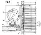
- FIG. 2shows a testing system of the prior art.
- FIGS. 1 a and 1 b of a testing system 1 of the invention for optical and electrical monitoring of the production quality and/or for determining optical and electrical properties of solar cells 2includes an optical checking device 3 , 3 ′, 3 ′′ for inspecting the solar cells 2 , which is located in a test region of the testing system 1 and in the present exemplary embodiment, among other things, includes optical monitoring for correctness and completeness of printed conductor elements on the surface of the solar cells 2 , checking for correct color and geometry of the solar cells 2 , and three-dimensional optical monitoring, for instance for splinters or other foreign bodies located in the printed conductor elements. Also located in the test region of the testing system 1 is an electrical checking device 4 for monitoring the electrical functions of the solar cells 2 .
- the illumination device 5for shining light on the light-sensitive surfaces of the solar cells 2 and an electrical contacting device 6 for picking up voltages and/or currents at electrical contacts of the solar cells 2 .
- the illumination device 5is located above and the electrical contacting device 6 is located below and/or above the solar cells 2 , traveling past it and to be checked, in the test region.
- the solar cells 2 to be monitoredare delivered to the test region by a first conveyor device, moved within the test region by a second conveyor device, and finally conveyed out of the test region by a third conveyor device.
- these three conveyor devicesinclude a common, linear conveyor belt system 7 , which in the present exemplary embodiment is constructed of a plurality of synchronously driven belt segments 7 a . . .
- the conveyor belt system 7has a vacuum suction device, not shown in detail in the drawing, for holding the solar cells 2 on a surface of the conveyor belt system.
- the solar cells 2 to be conveyedare thus held in a way secure against slipping, and moreover any waviness or unevenness of the solar cells 2 that may be present is smoothed, so that particularly their optical monitoring can be done without problems in the optical checking device 3 , 3 ′, 3 ′′.
- the conveyor belts of the conveyor belt system 7include three parallel belts, extending parallel to the conveying direction, of which at least the middle one has openings that are open toward the belt surface and communicate with the vacuum suction device.
- the electrical contacting device 6in particular can grasp the solar cells 2 to be checked, and moving past it, from below.
- the parallel belts of the conveyor belt system 7may also be moved independently of one another in the conveying direction.
- the optical checking device 3includes a area scanning camera 9 , which is located in a gap between successive belt segments 7 a , 7 b , and which as a position indicator cooperates with a discharge device, not shown in further detail, for separating the solar cells 2 that are supplied in stacks.
- the optical checking device 3 ′also has a portion (which in other embodiments may also be located in a gap in the belt, and) which includes a line scanning camera 9 ′.
- a line scanning camera 9 ′′may be provided for optically scanning the surface of the particularly solar cells 2 moving past it.
- Both the optical and the electrical checking of the solar cells 2can be done in operation with the belt moving, in particular continuously and without stopping the conveying of solar cells.
- the electrical checking device 4 and in particular its contacting device 6are designed such that checking the electrical functions of the solar cells 2 traveling past is done by means of contacts that in some portions move along with the solar cells and that after passing through the portion automatically return to their outset position.
- the electrical checkingcan be done in clocked fashion in each case in a stopped period between two conveying periods of the conveyor device.
- the testing system of the prior art described at the outset, shown schematically in FIG. 2includes a robot arm 10 , with which solar cells 2 supplied are taken from a first conveyor device 11 , designed as a conveyor belt, and are delivered to a second conveyor device, designed as a indexing turntable 12 .
- the indexing turntable 12conveys the solar cells 2 to be checked in clocked fashion to respective schematically shown optical and electrical measurement stations.
- the checked solar cell 2is taken by the robot arm 10 from the applicable station on the indexing turntable 12 and is transferred to a third conveyor device, designed as a transfer belt 13 , which transfers the solar cell to a sorter 14 , in which, depending on the quality class assigned it after the checking, it is sent for further processing or for shipment.
Landscapes
- General Physics & Mathematics (AREA)
- Physics & Mathematics (AREA)
- Engineering & Computer Science (AREA)
- Health & Medical Sciences (AREA)
- Chemical & Material Sciences (AREA)
- Computer Hardware Design (AREA)
- Microelectronics & Electronic Packaging (AREA)
- Power Engineering (AREA)
- Condensed Matter Physics & Semiconductors (AREA)
- Life Sciences & Earth Sciences (AREA)
- Manufacturing & Machinery (AREA)
- Analytical Chemistry (AREA)
- Biochemistry (AREA)
- General Health & Medical Sciences (AREA)
- Immunology (AREA)
- Pathology (AREA)
- Testing Of Individual Semiconductor Devices (AREA)
- Photovoltaic Devices (AREA)
Abstract
Description
Claims (21)
Applications Claiming Priority (3)
| Application Number | Priority Date | Filing Date | Title |
|---|---|---|---|
| DE102004050463ADE102004050463B3 (en) | 2004-10-16 | 2004-10-16 | Test system for solar cells |
| DE102004050463.6 | 2004-10-16 | ||
| DE102004050463 | 2004-10-16 |
Publications (2)
| Publication Number | Publication Date |
|---|---|
| US20060103371A1 US20060103371A1 (en) | 2006-05-18 |
| US7671620B2true US7671620B2 (en) | 2010-03-02 |
Family
ID=35510988
Family Applications (1)
| Application Number | Title | Priority Date | Filing Date |
|---|---|---|---|
| US11/249,298Expired - Fee RelatedUS7671620B2 (en) | 2004-10-16 | 2005-10-13 | Testing system for solar cells |
Country Status (5)
| Country | Link |
|---|---|
| US (1) | US7671620B2 (en) |
| EP (1) | EP1647827A1 (en) |
| KR (1) | KR100673138B1 (en) |
| CN (1) | CN100504422C (en) |
| DE (1) | DE102004050463B3 (en) |
Cited By (12)
| Publication number | Priority date | Publication date | Assignee | Title |
|---|---|---|---|---|
| US20090256581A1 (en)* | 2008-04-14 | 2009-10-15 | Applied Materials, Inc. | Solar parametric testing module and processes |
| US20110232059A1 (en)* | 2008-12-01 | 2011-09-29 | Thomas Rossmann | Method and device for fully automatically selecting and packing photovoltaic modules |
| US20120171807A1 (en)* | 2010-12-29 | 2012-07-05 | Berger Alexander J | Method and apparatus for masking substrates for deposition |
| US8664030B2 (en) | 1999-03-30 | 2014-03-04 | Daniel Luch | Collector grid and interconnect structures for photovoltaic arrays and modules |
| US8729385B2 (en) | 2006-04-13 | 2014-05-20 | Daniel Luch | Collector grid and interconnect structures for photovoltaic arrays and modules |
| US8822810B2 (en) | 2006-04-13 | 2014-09-02 | Daniel Luch | Collector grid and interconnect structures for photovoltaic arrays and modules |
| US8884155B2 (en) | 2006-04-13 | 2014-11-11 | Daniel Luch | Collector grid and interconnect structures for photovoltaic arrays and modules |
| US9006563B2 (en) | 2006-04-13 | 2015-04-14 | Solannex, Inc. | Collector grid and interconnect structures for photovoltaic arrays and modules |
| US9234843B2 (en) | 2011-08-25 | 2016-01-12 | Alliance For Sustainable Energy, Llc | On-line, continuous monitoring in solar cell and fuel cell manufacturing using spectral reflectance imaging |
| US9236512B2 (en) | 2006-04-13 | 2016-01-12 | Daniel Luch | Collector grid and interconnect structures for photovoltaic arrays and modules |
| US9865758B2 (en) | 2006-04-13 | 2018-01-09 | Daniel Luch | Collector grid and interconnect structures for photovoltaic arrays and modules |
| US10480935B2 (en) | 2016-12-02 | 2019-11-19 | Alliance For Sustainable Energy, Llc | Thickness mapping using multispectral imaging |
Families Citing this family (101)
| Publication number | Priority date | Publication date | Assignee | Title |
|---|---|---|---|---|
| DE10239845C1 (en)* | 2002-08-29 | 2003-12-24 | Day4 Energy Inc | Electrode for photovoltaic cells, photovoltaic cell and photovoltaic module |
| EP1710589A1 (en)* | 2005-03-30 | 2006-10-11 | VA TECH Transmission & Distribution SA | Optical sensor arrangement for electrical switchgear |
| US20070068567A1 (en)* | 2005-09-23 | 2007-03-29 | Rubin Leonid B | Testing apparatus and method for solar cells |
| DE102006037586A1 (en)* | 2006-08-11 | 2008-02-28 | Solarwatt Ag | Device and method for investigating the flow distribution in solar cells and solar modules |
| US20080092944A1 (en)* | 2006-10-16 | 2008-04-24 | Leonid Rubin | Semiconductor structure and process for forming ohmic connections to a semiconductor structure |
| US20080290368A1 (en)* | 2007-05-21 | 2008-11-27 | Day4 Energy, Inc. | Photovoltaic cell with shallow emitter |
| ITUD20070196A1 (en) | 2007-10-24 | 2009-04-25 | Baccini S P A | AUTOMATIC WAREHOUSE AND PROCEDURE FOR STORAGE OF ELECTRONIC CIRCUIT PLATES |
| US7667479B2 (en)* | 2007-10-31 | 2010-02-23 | Atomic Energy Council | Apparatus for testing concentration-type solar cells |
| JP2011507282A (en)* | 2007-12-18 | 2011-03-03 | デイ4 エネルギー インコーポレイテッド | SOLAR CELL MODULE, INTERCONNECT METHOD, DEVICE AND SYSTEM WITH EDGE ACCESSING UNIT TO PV STRING |
| US8138782B2 (en)* | 2008-01-10 | 2012-03-20 | Applied Materials, Inc. | Photovoltaic cell solar simulator |
| TW201006600A (en)* | 2008-04-10 | 2010-02-16 | Applied Materials Inc | Laser-scribing platform and hybrid writing strategy |
| CN101990481A (en)* | 2008-04-10 | 2011-03-23 | 应用材料股份有限公司 | Laser-scribing platform |
| US20090321399A1 (en)* | 2008-04-11 | 2009-12-31 | Applied Materials, Inc. | Dynamic scribe alignment for laser scribing, welding or any patterning system |
| WO2009126910A2 (en)* | 2008-04-11 | 2009-10-15 | Applied Materials, Inc. | Laser scribe inspection methods and systems |
| US20090314752A1 (en)* | 2008-05-14 | 2009-12-24 | Applied Materials, Inc. | In-situ monitoring for laser ablation |
| DE102008024000A1 (en) | 2008-05-18 | 2009-12-17 | Jonas & Redmann Automationstechnik Gmbh | Method for holding flat transporting goods, particularly substrates such as silicon wafer and solar cells at transporting surface of flat belt of conveyor, involves arranging electrical field with electrical potential difference |
| US20090308426A1 (en)* | 2008-06-11 | 2009-12-17 | Kent Kernahan | Method and apparatus for installing, testing, monitoring and activating power generation equipment |
| US7981778B2 (en)* | 2009-07-22 | 2011-07-19 | Applied Materials, Inc. | Directional solid phase crystallization of thin amorphous silicon for solar cell applications |
| US8293568B2 (en)* | 2008-07-28 | 2012-10-23 | Day4 Energy Inc. | Crystalline silicon PV cell with selective emitter produced with low temperature precision etch back and passivation process |
| GB0814406D0 (en)* | 2008-08-06 | 2008-09-10 | G24 Innovations Ltd | Testing photovoltaic transducers |
| KR20110059724A (en)* | 2008-08-26 | 2011-06-03 | 어플라이드 머티어리얼스, 인코포레이티드 | Laser material removal method and apparatus |
| WO2010039500A2 (en)* | 2008-09-23 | 2010-04-08 | Applied Materials, Inc. | Light soaking system and test method for solar cells |
| DE102008048834A1 (en)* | 2008-09-25 | 2010-04-08 | Schulz Systemtechnik Gmbh | Apparatus for testing solar cells |
| GB0821146D0 (en) | 2008-11-19 | 2008-12-24 | Univ Denmark Tech Dtu | Method of testing solar cells |
| WO2010059595A2 (en)* | 2008-11-19 | 2010-05-27 | Applied Materials, Inc. | Laser-scribing tool architecture |
| US20100212358A1 (en)* | 2009-02-26 | 2010-08-26 | Applied Materials, Inc. | Glass substrate orientation inspection methods and systems for photo voltaics production |
| DE102009012021B4 (en)* | 2009-03-10 | 2011-02-03 | Fraunhofer-Gesellschaft zur Förderung der angewandten Forschung e.V. | Measuring device for the electrical measurement of a measurement structure that can be electrically contacted on one side of a measurement side |
| US8333843B2 (en)* | 2009-04-16 | 2012-12-18 | Applied Materials, Inc. | Process to remove metal contamination on a glass substrate |
| US20100269853A1 (en)* | 2009-04-27 | 2010-10-28 | Applied Materials, Inc. | Debris-extraction exhaust system |
| KR101011493B1 (en)* | 2009-06-09 | 2011-01-31 | (유)에스엔티 | Solar cell manufacturing process system |
| WO2010144778A2 (en)* | 2009-06-12 | 2010-12-16 | Applied Materials, Inc. | Methods and systems for laser-scribed line alignment |
| US20100330711A1 (en)* | 2009-06-26 | 2010-12-30 | Applied Materials, Inc. | Method and apparatus for inspecting scribes in solar modules |
| EP2284520A1 (en)* | 2009-07-28 | 2011-02-16 | David Marcos Muntal | Assembly for the inspection in a continuous manner of cells, strings and photovoltaic modules and inspection method thereof |
| US20110139758A1 (en)* | 2009-08-06 | 2011-06-16 | Applied Materials, Inc. | Latitudinal iso-line scribe, stitching, and simplified laser and scanner controls |
| US20110198322A1 (en)* | 2009-08-06 | 2011-08-18 | Applied Materials, Inc. | In-line metrology methods and systems for solar cell fabrication |
| US8129658B2 (en)* | 2009-08-06 | 2012-03-06 | Applied Materials, Inc. | Systems for thin film laser scribing devices |
| WO2011017572A2 (en)* | 2009-08-06 | 2011-02-10 | Applied Materials, Inc. | Laser modules and processes for thin film solar panel laser scribing |
| US8228088B1 (en) | 2009-08-07 | 2012-07-24 | Brett Hinze | Automated solar module testing |
| IT1395561B1 (en) | 2009-09-03 | 2012-09-28 | Applied Materials Inc | TEST SYSTEM AND ITS PROCEDURE |
| US20110065227A1 (en)* | 2009-09-15 | 2011-03-17 | Applied Materials, Inc. | Common laser module for a photovoltaic production line |
| KR101020908B1 (en) | 2009-09-30 | 2011-03-09 | 엘지이노텍 주식회사 | Solar cell module and its detection method |
| US9595913B2 (en) | 2009-09-30 | 2017-03-14 | Lg Innotek Co., Ltd. | Solar cell apparatus |
| DE102009049705B3 (en)* | 2009-10-18 | 2011-05-12 | Harrexco Ag | Test device for a photovoltaic module plate, test equipment and methods for testing |
| CN101976698B (en)* | 2009-10-30 | 2012-04-04 | 浙江正泰太阳能科技有限公司 | Method for positioning and repairing defective cell in I-V curve abnormal solar cell module |
| US20110139755A1 (en)* | 2009-11-03 | 2011-06-16 | Applied Materials, Inc. | Multi-wavelength laser-scribing tool |
| US20110140726A1 (en)* | 2009-11-23 | 2011-06-16 | Applied Materials, Inc. | Apparatus and Methods for Measuring Solar Cell Module Performance |
| NL2003936C2 (en)* | 2009-12-10 | 2011-06-14 | Eurotron B V | METHOD AND DEVICE FOR MANUFACTURING SOLAR PANEL USING A CARRIER |
| US9525381B2 (en)* | 2011-09-26 | 2016-12-20 | First Solar, Inc. | Method and apparatus for electrically accessing photovoltaic modules |
| DE202010000325U1 (en)* | 2010-03-05 | 2011-08-26 | Kuka Systems Gmbh | service facility |
| DE202010000365U1 (en) | 2010-03-12 | 2011-08-30 | Kuka Systems Gmbh | test equipment |
| CN102201499A (en)* | 2010-03-25 | 2011-09-28 | 日本麦可罗尼克斯股份有限公司 | Electric processing apparatus and method, and detection unit |
| CN102384913A (en)* | 2010-09-02 | 2012-03-21 | 致茂电子(苏州)有限公司 | Solar wafer position calibrating device and detection machine station with the same |
| WO2012051695A1 (en)* | 2010-10-18 | 2012-04-26 | Day4 Energy Inc. | Testing apparatus for photovoltaic cells |
| KR101053065B1 (en)* | 2011-03-30 | 2011-08-01 | 한명전기주식회사 | Solar panel with junction box |
| US9863890B2 (en)* | 2011-06-10 | 2018-01-09 | The Boeing Company | Solar cell testing apparatus and method |
| US9513313B2 (en)* | 2011-06-14 | 2016-12-06 | Konica Minolta, Inc. | Method for inspecting electronic device and electronic device inspection apparatus |
| CN102721908A (en)* | 2012-06-29 | 2012-10-10 | 苏州晟成新能源科技有限公司 | Insulation tester with recognition function |
| CN102788941A (en)* | 2012-06-29 | 2012-11-21 | 苏州晟成新能源科技有限公司 | Insulation tester with centering device |
| CN102788938A (en)* | 2012-06-29 | 2012-11-21 | 苏州晟成新能源科技有限公司 | Insulation tester with rotatable display screen |
| CN102788940A (en)* | 2012-06-29 | 2012-11-21 | 苏州晟成新能源科技有限公司 | Insulation tester with adjustable conveying width |
| CN102788939B (en)* | 2012-06-29 | 2015-07-08 | 苏州晟成新能源科技有限公司 | Insulation tester with adjustable conveying length |
| DE102012017564B4 (en)* | 2012-09-05 | 2018-10-11 | Universität Konstanz | Device for non-permanent electrical contacting of solar cells for measuring electrical properties |
| JP6233602B2 (en)* | 2012-09-28 | 2017-11-22 | パナソニックIpマネジメント株式会社 | SOLAR CELL MODULE MANUFACTURING METHOD AND SOLAR CELL MODULE MANUFACTURING SYSTEM |
| US10090430B2 (en) | 2014-05-27 | 2018-10-02 | Sunpower Corporation | System for manufacturing a shingled solar cell module |
| US8952715B2 (en)* | 2012-11-14 | 2015-02-10 | Stratasense LLC | Wireless current-voltage tracer with uninterrupted bypass system and method |
| CN103344900B (en)* | 2013-07-03 | 2016-09-07 | 英利能源(中国)有限公司 | Photovoltaic battery panel electric performance test, data process and place method for separating and equipment |
| CN103399246B (en)* | 2013-08-29 | 2015-12-23 | 烟台市牟平海联联合有限责任公司 | A kind of electrical performance of cell detects and control system of classifying automatically |
| CN103675679B (en)* | 2013-12-05 | 2016-08-31 | 上海电机系统节能工程技术研究中心有限公司 | A kind of rollgang for motor full-automatic delivery test system |
| US11482639B2 (en) | 2014-05-27 | 2022-10-25 | Sunpower Corporation | Shingled solar cell module |
| KR102368110B1 (en)* | 2014-05-27 | 2022-02-25 | 선파워 코포레이션 | Shingled solar cell module |
| US11949026B2 (en) | 2014-05-27 | 2024-04-02 | Maxeon Solar Pte. Ltd. | Shingled solar cell module |
| CN106489211A (en)* | 2014-05-27 | 2017-03-08 | 太阳能公司 | Covered solar cell module |
| CN104085656A (en)* | 2014-06-30 | 2014-10-08 | 昆山爱都思电子科技有限公司 | Simultaneous-carrying plural-test cyclic automatic inspection system |
| TWI702732B (en) | 2014-10-20 | 2020-08-21 | 加拿大商奧羅拉太陽能技術(加拿大)有限公司 | Mapping of measurement data to production tool location and batch or time of processing |
| US10861999B2 (en) | 2015-04-21 | 2020-12-08 | Sunpower Corporation | Shingled solar cell module comprising hidden tap interconnects |
| CN104914379B (en)* | 2015-05-07 | 2017-08-25 | 浙江工商大学 | A kind of reverse-flow type full-automatic battery combo system based on dynamic optimization |
| CN104880674B (en)* | 2015-05-14 | 2018-01-19 | 苏州大源自动化科技股份有限公司 | A kind of battery on-line measuring device |
| CN106340563B (en)* | 2015-07-09 | 2017-10-10 | 英稳达科技股份有限公司 | How to make a solar cell |
| CN105259499B (en)* | 2015-10-30 | 2018-08-14 | 昆山鸿志犀自动化机电设备有限公司 | The linear automated test device to move in circles |
| CN105632957A (en)* | 2015-12-22 | 2016-06-01 | 中国电子科技集团公司第四十八研究所 | Method and device for testing battery slices |
| CN105719984A (en)* | 2016-02-22 | 2016-06-29 | 成都振中电气有限公司 | Solar cell performance detection system |
| CN105632966A (en)* | 2016-03-28 | 2016-06-01 | 成都振中电气有限公司 | Surface defect detection system of solar cell piece |
| CN108010983A (en)* | 2016-10-31 | 2018-05-08 | 无锡市瑞能科技有限公司 | Cell piece based on line scanning integrates detection module |
| DE102016224767B4 (en)* | 2016-12-13 | 2019-08-08 | Bayerische Motoren Werke Aktiengesellschaft | Device and method for detecting defects of a test object |
| CN108263848B (en)* | 2016-12-30 | 2019-07-16 | 中国科学院沈阳自动化研究所 | An automatic feeding device for battery cells |
| CN109088597A (en)* | 2018-08-02 | 2018-12-25 | 海宁奇瑞特光电有限公司 | A kind of photovoltaic module and its manufacturing method of recoverable heat |
| KR102626124B1 (en)* | 2018-11-13 | 2024-01-18 | 한국전력공사 | Apparatus evaluating solar cell |
| CN109828545B (en)* | 2019-02-28 | 2020-09-11 | 武汉三工智能装备制造有限公司 | AI intelligent process anomaly identification closed-loop control method, host and equipment system |
| CN109926341A (en)* | 2019-03-26 | 2019-06-25 | 武汉大学 | Silicon photrouics scanning vortex thermal imaging detection platform and defect classification method |
| CN111865215A (en)* | 2019-04-29 | 2020-10-30 | 北京铂阳顶荣光伏科技有限公司 | Detection device and method for solar cell |
| CN110665853B (en)* | 2019-09-20 | 2025-05-06 | 珠海冠宇电源有限公司 | Fully automatic laptop loading, testing, sorting and storage machine |
| DE102020102494A1 (en) | 2020-01-31 | 2021-08-05 | Heliatek Gmbh | Method for checking a photovoltaic element, as well as a photovoltaic element, checked according to such a method |
| CN112113618B (en)* | 2020-09-24 | 2024-10-11 | 武汉心浩智能科技有限公司 | Automatic testing device for circulator and isolator |
| CN112444695B (en)* | 2020-11-11 | 2022-06-28 | 安徽锦希自动化科技有限公司 | Detection apparatus for electrical automation equipment |
| CN112466768B (en)* | 2020-11-12 | 2022-05-24 | 东营大海科林光电有限公司 | Detection device and detection method for photovoltaic cell panel |
| CN112495812A (en)* | 2020-11-30 | 2021-03-16 | 广东新宇智能装备有限公司 | Voltage internal resistance test equipment of battery |
| CN115108318A (en)* | 2021-03-22 | 2022-09-27 | 江苏润阳光伏科技有限公司 | A kind of automatic conveying mechanism of manipulator handling roller shaft transmission device |
| DE102022116064A1 (en) | 2022-06-28 | 2023-12-28 | Wavelabs Solar Metrology Systems Gmbh | SOLAR CELL PRODUCTION PROCESS AND SOLAR CELL PRODUCTION PLANT |
| DE102022116102A1 (en) | 2022-06-28 | 2023-12-28 | Wavelabs Solar Metrology Systems Gmbh | SOLAR CELL TESTING PROCESS, SOLAR CELL PRODUCTION PROCESS, SOLAR CELL TESTING FACILITY AND SOLAR CELL PRODUCTION FACILITY |
| CN115931060B (en)* | 2023-03-13 | 2023-06-13 | 国网山西省电力公司晋中供电公司 | Storage battery monitoring device with alarm function |
| CN118399889B (en)* | 2024-04-29 | 2024-11-26 | 苏州柯派自动化设备有限公司 | A battery cell testing system and method |
Citations (16)
| Publication number | Priority date | Publication date | Assignee | Title |
|---|---|---|---|---|
| US3812947A (en) | 1969-07-29 | 1974-05-28 | Texas Instruments Inc | Automatic slice processing |
| US5460659A (en)* | 1993-12-10 | 1995-10-24 | Spectrolab, Inc. | Concentrating photovoltaic module and fabrication method |
| US5848868A (en) | 1996-04-22 | 1998-12-15 | Kabushiki Kaisha Shinkawa | Wafer conveying apparatus |
| US6154034A (en)* | 1998-10-20 | 2000-11-28 | Lovelady; James N. | Method and apparatus for testing photovoltaic solar cells using multiple pulsed light sources |
| US6183186B1 (en)* | 1997-08-29 | 2001-02-06 | Daitron, Inc. | Wafer handling system and method |
| JP2001091567A (en) | 1999-09-21 | 2001-04-06 | Mitsubishi Heavy Ind Ltd | Solar cell evaluating apparatus |
| US6265242B1 (en)* | 1998-02-23 | 2001-07-24 | Canon Kabushiki Kaisha | Solar cell module and a process for producing said solar cell module |
| US6359212B1 (en)* | 2000-07-13 | 2002-03-19 | Trw Inc. | Method for testing solar cell assemblies and second surface mirrors by ultraviolet reflectometry for susceptibility to ultraviolet degradation |
| US6362020B1 (en)* | 1998-01-30 | 2002-03-26 | Canon Kabushiki Kaisha | Process of forming deposited film, process of producing semiconductor element substrate, and process of producing photovoltaic element |
| US6590408B1 (en)* | 2002-05-29 | 2003-07-08 | Taiwan Semiconductor Manufacturing Co., Ltd. | Microelectronic fabrication electrical test apparatus and method providing enhanced electrical test accuracy |
| US6657447B1 (en)* | 2001-07-31 | 2003-12-02 | Xilnx, Inc. | Liquid crystal method to localize metal short on multi-layer metal CMOS process |
| US6731127B2 (en)* | 2001-12-21 | 2004-05-04 | Texas Instruments Incorporated | Parallel integrated circuit test apparatus and test method |
| US6798515B1 (en)* | 2001-11-29 | 2004-09-28 | Cognex Technology And Investment Corporation | Method for calculating a scale relationship for an imaging system |
| US6841725B2 (en)* | 2002-08-13 | 2005-01-11 | David F. Fortuna | Measure minder |
| US6944324B2 (en)* | 2000-01-24 | 2005-09-13 | Robotic Vision Systems, Inc. | Machine vision-based singulation verification system and method |
| US6946858B2 (en)* | 2002-07-26 | 2005-09-20 | Canon Kabushiki Kaisha | Method and apparatus for measuring photoelectric conversion device, and process and apparatus for producing photoelectric conversion device |
Family Cites Families (8)
| Publication number | Priority date | Publication date | Assignee | Title |
|---|---|---|---|---|
| CA931024A (en)* | 1970-12-19 | 1973-07-31 | H. Prange Bernard | Method and apparatus for silk screening a pattern on an underlying substrate |
| AU2095083A (en)* | 1982-11-09 | 1984-05-17 | Energy Conversion Devices Inc. | Laminated strip of large area solar cells |
| US4561541A (en)* | 1983-09-26 | 1985-12-31 | Spectrolab, Incorporated | Carrier system for photovoltaic cells |
| JP2788604B2 (en)* | 1994-06-20 | 1998-08-20 | インターナショナル・ビジネス・マシーンズ・コーポレイション | Information display tag having two-dimensional information pattern, image processing method and image processing apparatus using the same |
| US5863412A (en)* | 1995-10-17 | 1999-01-26 | Canon Kabushiki Kaisha | Etching method and process for producing a semiconductor element using said etching method |
| JP4461625B2 (en)* | 2001-03-13 | 2010-05-12 | 富士電機ホールディングス株式会社 | Method and apparatus for continuous automatic measurement of solar cell characteristics |
| JP3809353B2 (en)* | 2001-08-02 | 2006-08-16 | キヤノン株式会社 | Manufacturing method of workpiece with ID |
| JP2003065727A (en)* | 2001-08-28 | 2003-03-05 | Mitsubishi Heavy Ind Ltd | Device for measuring thickness of transmissive film and film producing apparatus employing the same |
- 2004
- 2004-10-16DEDE102004050463Apatent/DE102004050463B3/ennot_activeExpired - Fee Related
- 2005
- 2005-10-07EPEP05021867Apatent/EP1647827A1/ennot_activeCeased
- 2005-10-13USUS11/249,298patent/US7671620B2/ennot_activeExpired - Fee Related
- 2005-10-14CNCNB2005101249722Apatent/CN100504422C/ennot_activeExpired - Fee Related
- 2005-10-15KRKR1020050097253Apatent/KR100673138B1/ennot_activeExpired - Fee Related
Patent Citations (16)
| Publication number | Priority date | Publication date | Assignee | Title |
|---|---|---|---|---|
| US3812947A (en) | 1969-07-29 | 1974-05-28 | Texas Instruments Inc | Automatic slice processing |
| US5460659A (en)* | 1993-12-10 | 1995-10-24 | Spectrolab, Inc. | Concentrating photovoltaic module and fabrication method |
| US5848868A (en) | 1996-04-22 | 1998-12-15 | Kabushiki Kaisha Shinkawa | Wafer conveying apparatus |
| US6183186B1 (en)* | 1997-08-29 | 2001-02-06 | Daitron, Inc. | Wafer handling system and method |
| US6362020B1 (en)* | 1998-01-30 | 2002-03-26 | Canon Kabushiki Kaisha | Process of forming deposited film, process of producing semiconductor element substrate, and process of producing photovoltaic element |
| US6265242B1 (en)* | 1998-02-23 | 2001-07-24 | Canon Kabushiki Kaisha | Solar cell module and a process for producing said solar cell module |
| US6154034A (en)* | 1998-10-20 | 2000-11-28 | Lovelady; James N. | Method and apparatus for testing photovoltaic solar cells using multiple pulsed light sources |
| JP2001091567A (en) | 1999-09-21 | 2001-04-06 | Mitsubishi Heavy Ind Ltd | Solar cell evaluating apparatus |
| US6944324B2 (en)* | 2000-01-24 | 2005-09-13 | Robotic Vision Systems, Inc. | Machine vision-based singulation verification system and method |
| US6359212B1 (en)* | 2000-07-13 | 2002-03-19 | Trw Inc. | Method for testing solar cell assemblies and second surface mirrors by ultraviolet reflectometry for susceptibility to ultraviolet degradation |
| US6657447B1 (en)* | 2001-07-31 | 2003-12-02 | Xilnx, Inc. | Liquid crystal method to localize metal short on multi-layer metal CMOS process |
| US6798515B1 (en)* | 2001-11-29 | 2004-09-28 | Cognex Technology And Investment Corporation | Method for calculating a scale relationship for an imaging system |
| US6731127B2 (en)* | 2001-12-21 | 2004-05-04 | Texas Instruments Incorporated | Parallel integrated circuit test apparatus and test method |
| US6590408B1 (en)* | 2002-05-29 | 2003-07-08 | Taiwan Semiconductor Manufacturing Co., Ltd. | Microelectronic fabrication electrical test apparatus and method providing enhanced electrical test accuracy |
| US6946858B2 (en)* | 2002-07-26 | 2005-09-20 | Canon Kabushiki Kaisha | Method and apparatus for measuring photoelectric conversion device, and process and apparatus for producing photoelectric conversion device |
| US6841725B2 (en)* | 2002-08-13 | 2005-01-11 | David F. Fortuna | Measure minder |
Cited By (15)
| Publication number | Priority date | Publication date | Assignee | Title |
|---|---|---|---|---|
| US8664030B2 (en) | 1999-03-30 | 2014-03-04 | Daniel Luch | Collector grid and interconnect structures for photovoltaic arrays and modules |
| US9006563B2 (en) | 2006-04-13 | 2015-04-14 | Solannex, Inc. | Collector grid and interconnect structures for photovoltaic arrays and modules |
| US9236512B2 (en) | 2006-04-13 | 2016-01-12 | Daniel Luch | Collector grid and interconnect structures for photovoltaic arrays and modules |
| US9865758B2 (en) | 2006-04-13 | 2018-01-09 | Daniel Luch | Collector grid and interconnect structures for photovoltaic arrays and modules |
| US8884155B2 (en) | 2006-04-13 | 2014-11-11 | Daniel Luch | Collector grid and interconnect structures for photovoltaic arrays and modules |
| US8822810B2 (en) | 2006-04-13 | 2014-09-02 | Daniel Luch | Collector grid and interconnect structures for photovoltaic arrays and modules |
| US8729385B2 (en) | 2006-04-13 | 2014-05-20 | Daniel Luch | Collector grid and interconnect structures for photovoltaic arrays and modules |
| US20090256581A1 (en)* | 2008-04-14 | 2009-10-15 | Applied Materials, Inc. | Solar parametric testing module and processes |
| US8049521B2 (en)* | 2008-04-14 | 2011-11-01 | Applied Materials, Inc. | Solar parametric testing module and processes |
| US20110232059A1 (en)* | 2008-12-01 | 2011-09-29 | Thomas Rossmann | Method and device for fully automatically selecting and packing photovoltaic modules |
| US9379661B2 (en) | 2008-12-01 | 2016-06-28 | Grenzebach Maschinenbau Gmbh | Method and device for fully automatically selecting and packing photovoltaic modules |
| US8677929B2 (en)* | 2010-12-29 | 2014-03-25 | Intevac, Inc. | Method and apparatus for masking solar cell substrates for deposition |
| US20120171807A1 (en)* | 2010-12-29 | 2012-07-05 | Berger Alexander J | Method and apparatus for masking substrates for deposition |
| US9234843B2 (en) | 2011-08-25 | 2016-01-12 | Alliance For Sustainable Energy, Llc | On-line, continuous monitoring in solar cell and fuel cell manufacturing using spectral reflectance imaging |
| US10480935B2 (en) | 2016-12-02 | 2019-11-19 | Alliance For Sustainable Energy, Llc | Thickness mapping using multispectral imaging |
Also Published As
| Publication number | Publication date |
|---|---|
| DE102004050463B3 (en) | 2006-04-20 |
| KR20060054028A (en) | 2006-05-22 |
| CN100504422C (en) | 2009-06-24 |
| EP1647827A1 (en) | 2006-04-19 |
| KR100673138B1 (en) | 2007-01-22 |
| CN1769920A (en) | 2006-05-10 |
| US20060103371A1 (en) | 2006-05-18 |
Similar Documents
| Publication | Publication Date | Title |
|---|---|---|
| US7671620B2 (en) | Testing system for solar cells | |
| CN109709106B (en) | Inspection system and method for analyzing defects | |
| US4851902A (en) | Auatomatic inspection system for IC lead frames and visual inspection method thereof | |
| TWI682487B (en) | Component centralization | |
| JP2003528323A (en) | Circuit board tester | |
| CN110385278B (en) | Automobile steering gear sleeve detection device | |
| US10937683B1 (en) | Conveyor inspection system, substrate rotator, and test system having the same | |
| CN103084341A (en) | Substrate inspection apparatus | |
| KR20050032530A (en) | Automatic inspection apparatus of substrate for semiconductor package | |
| JPH04107000A (en) | Part appearance selector | |
| JPH01250845A (en) | Automatic external appearance inspection machine for chip-shaped component | |
| US20240429078A1 (en) | Inspection system | |
| KR20180010492A (en) | Vision inspection module and device handler having the same | |
| TWM448687U (en) | Testing apparatus with turn-over device | |
| WO2010071609A2 (en) | System and processing of a substrate | |
| CN109225918A (en) | A kind of interior star-wheel loading and unloading detection device | |
| CN100459086C (en) | Method and apparatus for testing electronic components | |
| CN108449975A (en) | Visual inspection module and component inspection system including this module | |
| CN206002457U (en) | Noble metal check machine | |
| US6311886B1 (en) | Position and direction sensing system for an inspection and handling system | |
| CN114871126B (en) | Shell size detection device | |
| KR20150069144A (en) | Method for Inspecting Lead Frame of LED | |
| CN114365272A (en) | Conveyor inspection system, substrate rotator, and test system having the same | |
| WO2023200368A1 (en) | Arrangement of a system for in-line quality control and sorting of individual articles | |
| WO2021066984A1 (en) | Conveyor inspection system, substrate rotator, and test system having the same |
Legal Events
| Date | Code | Title | Description |
|---|---|---|---|
| AS | Assignment | Owner name:MANZ AUTOMATION AG,GERMANY Free format text:ASSIGNMENT OF ASSIGNORS INTEREST;ASSIGNOR:MANZ, DIETER;REEL/FRAME:016830/0381 Effective date:20051017 Owner name:MANZ AUTOMATION AG, GERMANY Free format text:ASSIGNMENT OF ASSIGNORS INTEREST;ASSIGNOR:MANZ, DIETER;REEL/FRAME:016830/0381 Effective date:20051017 | |
| STCF | Information on status: patent grant | Free format text:PATENTED CASE | |
| FPAY | Fee payment | Year of fee payment:4 | |
| FEPP | Fee payment procedure | Free format text:PAYOR NUMBER ASSIGNED (ORIGINAL EVENT CODE: ASPN); ENTITY STATUS OF PATENT OWNER: LARGE ENTITY | |
| MAFP | Maintenance fee payment | Free format text:PAYMENT OF MAINTENANCE FEE, 8TH YEAR, LARGE ENTITY (ORIGINAL EVENT CODE: M1552) Year of fee payment:8 | |
| FEPP | Fee payment procedure | Free format text:MAINTENANCE FEE REMINDER MAILED (ORIGINAL EVENT CODE: REM.); ENTITY STATUS OF PATENT OWNER: LARGE ENTITY | |
| LAPS | Lapse for failure to pay maintenance fees | Free format text:PATENT EXPIRED FOR FAILURE TO PAY MAINTENANCE FEES (ORIGINAL EVENT CODE: EXP.); ENTITY STATUS OF PATENT OWNER: LARGE ENTITY | |
| STCH | Information on status: patent discontinuation | Free format text:PATENT EXPIRED DUE TO NONPAYMENT OF MAINTENANCE FEES UNDER 37 CFR 1.362 | |
| FP | Lapsed due to failure to pay maintenance fee | Effective date:20220302 |