US7670758B2 - Optical films and methods of making the same - Google Patents
Optical films and methods of making the sameDownload PDFInfo
- Publication number
- US7670758B2 US7670758B2US11/139,954US13995405AUS7670758B2US 7670758 B2US7670758 B2US 7670758B2US 13995405 AUS13995405 AUS 13995405AUS 7670758 B2US7670758 B2US 7670758B2
- Authority
- US
- United States
- Prior art keywords
- less
- layer
- portions
- grating
- precursor
- Prior art date
- Legal status (The legal status is an assumption and is not a legal conclusion. Google has not performed a legal analysis and makes no representation as to the accuracy of the status listed.)
- Expired - Lifetime
Links
- 238000000034methodMethods0.000titleclaimsabstractdescription54
- 239000012788optical filmSubstances0.000titledescription4
- 239000010410layerSubstances0.000claimsdescription218
- 239000000463materialSubstances0.000claimsdescription136
- 239000002243precursorSubstances0.000claimsdescription74
- 239000002356single layerSubstances0.000claimsdescription59
- 239000003153chemical reaction reagentSubstances0.000claimsdescription48
- 230000005855radiationEffects0.000claimsdescription46
- VYPSYNLAJGMNEJ-UHFFFAOYSA-NSilicium dioxideChemical compoundO=[Si]=OVYPSYNLAJGMNEJ-UHFFFAOYSA-N0.000claimsdescription35
- 229910052751metalInorganic materials0.000claimsdescription29
- 239000002184metalSubstances0.000claimsdescription29
- 238000000151depositionMethods0.000claimsdescription22
- 229910052681coesiteInorganic materials0.000claimsdescription16
- 229910052906cristobaliteInorganic materials0.000claimsdescription16
- 239000000377silicon dioxideSubstances0.000claimsdescription16
- 229910052682stishoviteInorganic materials0.000claimsdescription16
- 229910052905tridymiteInorganic materials0.000claimsdescription16
- 229910052782aluminiumInorganic materials0.000claimsdescription8
- 229910052802copperInorganic materials0.000claimsdescription7
- 229910052737goldInorganic materials0.000claimsdescription7
- 239000003989dielectric materialSubstances0.000claimsdescription6
- 238000011049fillingMethods0.000claimsdescription6
- 229910052709silverInorganic materials0.000claimsdescription6
- 230000003287optical effectEffects0.000abstractdescription26
- 239000000758substrateSubstances0.000description48
- 230000010287polarizationEffects0.000description40
- 239000010408filmSubstances0.000description33
- GWEVSGVZZGPLCZ-UHFFFAOYSA-NTitan oxideChemical compoundO=[Ti]=OGWEVSGVZZGPLCZ-UHFFFAOYSA-N0.000description22
- 238000005530etchingMethods0.000description21
- 238000000231atomic layer depositionMethods0.000description18
- 239000007789gasSubstances0.000description14
- 230000008021depositionEffects0.000description13
- 230000005540biological transmissionEffects0.000description11
- 238000003491arrayMethods0.000description10
- 239000000203mixtureSubstances0.000description10
- 238000000025interference lithographyMethods0.000description9
- 238000010926purgeMethods0.000description9
- 239000006227byproductSubstances0.000description8
- 239000012159carrier gasSubstances0.000description8
- 238000006243chemical reactionMethods0.000description8
- 238000001228spectrumMethods0.000description8
- 230000001902propagating effectEffects0.000description7
- 238000004544sputter depositionMethods0.000description7
- MCMNRKCIXSYSNV-UHFFFAOYSA-NZirconium dioxideChemical compoundO=[Zr]=OMCMNRKCIXSYSNV-UHFFFAOYSA-N0.000description6
- VSCWAEJMTAWNJL-UHFFFAOYSA-Kaluminium trichlorideChemical compoundCl[Al](Cl)ClVSCWAEJMTAWNJL-UHFFFAOYSA-K0.000description6
- 238000005229chemical vapour depositionMethods0.000description6
- 238000005137deposition processMethods0.000description6
- 238000001704evaporationMethods0.000description6
- ZKATWMILCYLAPD-UHFFFAOYSA-Nniobium pentoxideChemical compoundO=[Nb](=O)O[Nb](=O)=OZKATWMILCYLAPD-UHFFFAOYSA-N0.000description6
- PBCFLUZVCVVTBY-UHFFFAOYSA-Ntantalum pentoxideInorganic materialsO=[Ta](=O)O[Ta](=O)=OPBCFLUZVCVVTBY-UHFFFAOYSA-N0.000description6
- XLYOFNOQVPJJNP-UHFFFAOYSA-NwaterChemical compoundOXLYOFNOQVPJJNP-UHFFFAOYSA-N0.000description6
- 238000010521absorption reactionMethods0.000description5
- QVGXLLKOCUKJST-UHFFFAOYSA-Natomic oxygenChemical compound[O]QVGXLLKOCUKJST-UHFFFAOYSA-N0.000description5
- 238000010586diagramMethods0.000description5
- 238000005566electron beam evaporationMethods0.000description5
- CJNBYAVZURUTKZ-UHFFFAOYSA-Nhafnium(IV) oxideInorganic materialsO=[Hf]=OCJNBYAVZURUTKZ-UHFFFAOYSA-N0.000description5
- 230000002452interceptive effectEffects0.000description5
- -1metal fluorides)Chemical class0.000description5
- 238000001127nanoimprint lithographyMethods0.000description5
- 239000001301oxygenSubstances0.000description5
- 229910052760oxygenInorganic materials0.000description5
- 238000001020plasma etchingMethods0.000description5
- 238000002310reflectometryMethods0.000description5
- XKRFYHLGVUSROY-UHFFFAOYSA-NArgonChemical compound[Ar]XKRFYHLGVUSROY-UHFFFAOYSA-N0.000description4
- PEDCQBHIVMGVHV-UHFFFAOYSA-NGlycerineChemical compoundOCC(O)COPEDCQBHIVMGVHV-UHFFFAOYSA-N0.000description4
- 229910003074TiCl4Inorganic materials0.000description4
- PNEYBMLMFCGWSK-UHFFFAOYSA-Naluminium oxideInorganic materials[O-2].[O-2].[O-2].[Al+3].[Al+3]PNEYBMLMFCGWSK-UHFFFAOYSA-N0.000description4
- 229910052804chromiumInorganic materials0.000description4
- 229910052593corundumInorganic materials0.000description4
- 239000011521glassSubstances0.000description4
- PSCMQHVBLHHWTO-UHFFFAOYSA-Kindium(iii) chlorideChemical compoundCl[In](Cl)ClPSCMQHVBLHHWTO-UHFFFAOYSA-K0.000description4
- 239000011147inorganic materialSubstances0.000description4
- 239000004973liquid crystal related substanceSubstances0.000description4
- 238000002161passivationMethods0.000description4
- 230000000737periodic effectEffects0.000description4
- 238000007493shaping processMethods0.000description4
- XJDNKRIXUMDJCW-UHFFFAOYSA-Jtitanium tetrachlorideChemical compoundCl[Ti](Cl)(Cl)ClXJDNKRIXUMDJCW-UHFFFAOYSA-J0.000description4
- JLTRXTDYQLMHGR-UHFFFAOYSA-NtrimethylaluminiumChemical compoundC[Al](C)CJLTRXTDYQLMHGR-UHFFFAOYSA-N0.000description4
- 229910001845yogo sapphireInorganic materials0.000description4
- LFQSCWFLJHTTHZ-UHFFFAOYSA-NEthanolChemical compoundCCOLFQSCWFLJHTTHZ-UHFFFAOYSA-N0.000description3
- 229910004205SiNXInorganic materials0.000description3
- 230000008901benefitEffects0.000description3
- 230000008033biological extinctionEffects0.000description3
- 238000000576coating methodMethods0.000description3
- 238000001816coolingMethods0.000description3
- 235000019441ethanolNutrition0.000description3
- 230000008020evaporationEffects0.000description3
- 239000012535impuritySubstances0.000description3
- 229910010272inorganic materialInorganic materials0.000description3
- 238000000869ion-assisted depositionMethods0.000description3
- 239000007788liquidSubstances0.000description3
- 229910001635magnesium fluorideInorganic materials0.000description3
- 238000004519manufacturing processMethods0.000description3
- 150000002739metalsChemical class0.000description3
- 239000011368organic materialSubstances0.000description3
- 239000007800oxidant agentSubstances0.000description3
- 238000000623plasma-assisted chemical vapour depositionMethods0.000description3
- 229920000642polymerPolymers0.000description3
- 230000002829reductive effectEffects0.000description3
- CSCPPACGZOOCGX-UHFFFAOYSA-NAcetoneChemical compoundCC(C)=OCSCPPACGZOOCGX-UHFFFAOYSA-N0.000description2
- IJGRMHOSHXDMSA-UHFFFAOYSA-NAtomic nitrogenChemical compoundN#NIJGRMHOSHXDMSA-UHFFFAOYSA-N0.000description2
- KZBUYRJDOAKODT-UHFFFAOYSA-NChlorineChemical compoundClClKZBUYRJDOAKODT-UHFFFAOYSA-N0.000description2
- 229910003865HfCl4Inorganic materials0.000description2
- MHAJPDPJQMAIIY-UHFFFAOYSA-NHydrogen peroxideChemical compoundOOMHAJPDPJQMAIIY-UHFFFAOYSA-N0.000description2
- CBENFWSGALASAD-UHFFFAOYSA-NOzoneChemical compound[O-][O+]=OCBENFWSGALASAD-UHFFFAOYSA-N0.000description2
- 229910003910SiCl4Inorganic materials0.000description2
- 229910003818SiH2Cl2Inorganic materials0.000description2
- BOTDANWDWHJENH-UHFFFAOYSA-NTetraethyl orthosilicateChemical compoundCCO[Si](OCC)(OCC)OCCBOTDANWDWHJENH-UHFFFAOYSA-N0.000description2
- XLOMVQKBTHCTTD-UHFFFAOYSA-NZinc monoxideChemical compound[Zn]=OXLOMVQKBTHCTTD-UHFFFAOYSA-N0.000description2
- XAGFODPZIPBFFR-UHFFFAOYSA-NaluminiumChemical compound[Al]XAGFODPZIPBFFR-UHFFFAOYSA-N0.000description2
- 229910052786argonInorganic materials0.000description2
- 230000000712assemblyEffects0.000description2
- 238000000429assemblyMethods0.000description2
- 239000011248coating agentSubstances0.000description2
- 230000001427coherent effectEffects0.000description2
- 239000000470constituentSubstances0.000description2
- 239000013078crystalSubstances0.000description2
- 239000002178crystalline materialSubstances0.000description2
- 150000002222fluorine compoundsChemical class0.000description2
- 235000011187glycerolNutrition0.000description2
- PDPJQWYGJJBYLF-UHFFFAOYSA-Jhafnium tetrachlorideChemical compoundCl[Hf](Cl)(Cl)ClPDPJQWYGJJBYLF-UHFFFAOYSA-J0.000description2
- 238000007654immersionMethods0.000description2
- 238000010884ion-beam techniqueMethods0.000description2
- 150000002500ionsChemical class0.000description2
- 238000001459lithographyMethods0.000description2
- 238000002156mixingMethods0.000description2
- 150000004767nitridesChemical class0.000description2
- 150000002894organic compoundsChemical class0.000description2
- 230000001590oxidative effectEffects0.000description2
- 229920002120photoresistant polymerPolymers0.000description2
- 229920003229poly(methyl methacrylate)Polymers0.000description2
- 239000004926polymethyl methacrylateSubstances0.000description2
- 239000004065semiconductorSubstances0.000description2
- FDNAPBUWERUEDA-UHFFFAOYSA-Nsilicon tetrachlorideChemical compoundCl[Si](Cl)(Cl)ClFDNAPBUWERUEDA-UHFFFAOYSA-N0.000description2
- 239000002904solventSubstances0.000description2
- 238000001179sorption measurementMethods0.000description2
- 239000000126substanceSubstances0.000description2
- XOLBLPGZBRYERU-UHFFFAOYSA-Ntin dioxideChemical compoundO=[Sn]=OXOLBLPGZBRYERU-UHFFFAOYSA-N0.000description2
- RZVAJINKPMORJF-UHFFFAOYSA-NAcetaminophenChemical compoundCC(=O)NC1=CC=C(O)C=C1RZVAJINKPMORJF-UHFFFAOYSA-N0.000description1
- 102000052666B-Cell Lymphoma 3Human genes0.000description1
- 108700009171B-Cell Lymphoma 3Proteins0.000description1
- 101150072667Bcl3 geneProteins0.000description1
- ZAMOUSCENKQFHK-UHFFFAOYSA-NChlorine atomChemical compound[Cl]ZAMOUSCENKQFHK-UHFFFAOYSA-N0.000description1
- 229910001218Gallium arsenideInorganic materials0.000description1
- 229910003327LiNbO3Inorganic materials0.000description1
- OKKJLVBELUTLKV-UHFFFAOYSA-NMethanolChemical compoundOCOKKJLVBELUTLKV-UHFFFAOYSA-N0.000description1
- 239000004793PolystyreneSubstances0.000description1
- ATJFFYVFTNAWJD-UHFFFAOYSA-NTinChemical compound[Sn]ATJFFYVFTNAWJD-UHFFFAOYSA-N0.000description1
- 239000007983Tris bufferSubstances0.000description1
- 229910007932ZrCl4Inorganic materials0.000description1
- 239000002253acidSubstances0.000description1
- 150000007513acidsChemical class0.000description1
- 239000000853adhesiveSubstances0.000description1
- 230000001070adhesive effectEffects0.000description1
- 230000002411adverseEffects0.000description1
- 150000001298alcoholsChemical class0.000description1
- 239000005354aluminosilicate glassSubstances0.000description1
- 229910021486amorphous silicon dioxideInorganic materials0.000description1
- 238000004380ashingMethods0.000description1
- 230000009286beneficial effectEffects0.000description1
- 230000000903blocking effectEffects0.000description1
- 239000005388borosilicate glassSubstances0.000description1
- 230000015556catabolic processEffects0.000description1
- 239000007795chemical reaction productSubstances0.000description1
- 239000000460chlorineSubstances0.000description1
- 229910052801chlorineInorganic materials0.000description1
- 150000001805chlorine compoundsChemical class0.000description1
- 238000004140cleaningMethods0.000description1
- 238000004891communicationMethods0.000description1
- 150000001875compoundsChemical class0.000description1
- 229910021419crystalline siliconInorganic materials0.000description1
- 230000007423decreaseEffects0.000description1
- 238000006731degradation reactionMethods0.000description1
- 230000000694effectsEffects0.000description1
- 238000001493electron microscopyMethods0.000description1
- 238000000609electron-beam lithographyMethods0.000description1
- 238000000572ellipsometryMethods0.000description1
- 230000007613environmental effectEffects0.000description1
- 239000012530fluidSubstances0.000description1
- 239000005350fused silica glassSubstances0.000description1
- 239000002223garnetSubstances0.000description1
- 239000001307heliumSubstances0.000description1
- 229910052734heliumInorganic materials0.000description1
- SWQJXJOGLNCZEY-UHFFFAOYSA-Nhelium atomChemical compound[He]SWQJXJOGLNCZEY-UHFFFAOYSA-N0.000description1
- ORJFXWYTRPGGRK-UHFFFAOYSA-Nhydroxy-tris(2-methylbutan-2-yloxy)silaneChemical compoundCCC(C)(C)O[Si](O)(OC(C)(C)CC)OC(C)(C)CCORJFXWYTRPGGRK-UHFFFAOYSA-N0.000description1
- HLDBBQREZCVBMA-UHFFFAOYSA-Nhydroxy-tris[(2-methylpropan-2-yl)oxy]silaneChemical compoundCC(C)(C)O[Si](O)(OC(C)(C)C)OC(C)(C)CHLDBBQREZCVBMA-UHFFFAOYSA-N0.000description1
- 238000003384imaging methodMethods0.000description1
- PJXISJQVUVHSOJ-UHFFFAOYSA-Nindium(III) oxideInorganic materials[O-2].[O-2].[O-2].[In+3].[In+3]PJXISJQVUVHSOJ-UHFFFAOYSA-N0.000description1
- 230000003993interactionEffects0.000description1
- 229910052743kryptonInorganic materials0.000description1
- DNNSSWSSYDEUBZ-UHFFFAOYSA-Nkrypton atomChemical compound[Kr]DNNSSWSSYDEUBZ-UHFFFAOYSA-N0.000description1
- 230000000873masking effectEffects0.000description1
- 238000005259measurementMethods0.000description1
- 229910001510metal chlorideInorganic materials0.000description1
- 229910001512metal fluorideInorganic materials0.000description1
- 229910001092metal group alloyInorganic materials0.000description1
- 229910044991metal oxideInorganic materials0.000description1
- 150000004706metal oxidesChemical class0.000description1
- 238000001465metallisationMethods0.000description1
- 239000002086nanomaterialSubstances0.000description1
- 229910052754neonInorganic materials0.000description1
- GKAOGPIIYCISHV-UHFFFAOYSA-Nneon atomChemical compound[Ne]GKAOGPIIYCISHV-UHFFFAOYSA-N0.000description1
- 229910052759nickelInorganic materials0.000description1
- 229910052757nitrogenInorganic materials0.000description1
- 239000003960organic solventSubstances0.000description1
- 238000007254oxidation reactionMethods0.000description1
- 238000000206photolithographyMethods0.000description1
- 239000004033plasticSubstances0.000description1
- 229920003023plasticPolymers0.000description1
- 238000005498polishingMethods0.000description1
- 238000002360preparation methodMethods0.000description1
- 239000011241protective layerSubstances0.000description1
- 239000005297pyrexSubstances0.000description1
- 239000010453quartzSubstances0.000description1
- 239000000376reactantSubstances0.000description1
- 238000005070samplingMethods0.000description1
- 229920006395saturated elastomerPolymers0.000description1
- HYXGAEYDKFCVMU-UHFFFAOYSA-Nscandium(III) oxideInorganic materialsO=[Sc]O[Sc]=OHYXGAEYDKFCVMU-UHFFFAOYSA-N0.000description1
- SCPYDCQAZCOKTP-UHFFFAOYSA-NsilanolChemical compound[SiH3]OSCPYDCQAZCOKTP-UHFFFAOYSA-N0.000description1
- 229910052814silicon oxideInorganic materials0.000description1
- 229910052950sphaleriteInorganic materials0.000description1
- 230000001360synchronised effectEffects0.000description1
- 125000004213tert-butoxy groupChemical group[H]C([H])([H])C(O*)(C([H])([H])[H])C([H])([H])[H]0.000description1
- 238000002207thermal evaporationMethods0.000description1
- 239000012815thermoplastic materialSubstances0.000description1
- 239000010409thin filmSubstances0.000description1
- 150000003568thioethersChemical class0.000description1
- 229910052719titaniumInorganic materials0.000description1
- 230000001131transforming effectEffects0.000description1
- LENZDBCJOHFCAS-UHFFFAOYSA-NtrisChemical compoundOCC(N)(CO)COLENZDBCJOHFCAS-UHFFFAOYSA-N0.000description1
- 238000001771vacuum depositionMethods0.000description1
- 238000001429visible spectrumMethods0.000description1
- 239000002699waste materialSubstances0.000description1
- 238000001039wet etchingMethods0.000description1
- 229910052724xenonInorganic materials0.000description1
- FHNFHKCVQCLJFQ-UHFFFAOYSA-Nxenon atomChemical compound[Xe]FHNFHKCVQCLJFQ-UHFFFAOYSA-N0.000description1
- 229910052984zinc sulfideInorganic materials0.000description1
- DUNKXUFBGCUVQW-UHFFFAOYSA-Jzirconium tetrachlorideChemical compoundCl[Zr](Cl)(Cl)ClDUNKXUFBGCUVQW-UHFFFAOYSA-J0.000description1
Images


Classifications
- G—PHYSICS
- G02—OPTICS
- G02B—OPTICAL ELEMENTS, SYSTEMS OR APPARATUS
- G02B5/00—Optical elements other than lenses
- G02B5/30—Polarising elements
- G02B5/3025—Polarisers, i.e. arrangements capable of producing a definite output polarisation state from an unpolarised input state
- G—PHYSICS
- G02—OPTICS
- G02B—OPTICAL ELEMENTS, SYSTEMS OR APPARATUS
- G02B5/00—Optical elements other than lenses
- G02B5/30—Polarising elements
- B—PERFORMING OPERATIONS; TRANSPORTING
- B05—SPRAYING OR ATOMISING IN GENERAL; APPLYING FLUENT MATERIALS TO SURFACES, IN GENERAL
- B05D—PROCESSES FOR APPLYING FLUENT MATERIALS TO SURFACES, IN GENERAL
- B05D5/00—Processes for applying liquids or other fluent materials to surfaces to obtain special surface effects, finishes or structures
- B05D5/06—Processes for applying liquids or other fluent materials to surfaces to obtain special surface effects, finishes or structures to obtain multicolour or other optical effects
- B—PERFORMING OPERATIONS; TRANSPORTING
- B29—WORKING OF PLASTICS; WORKING OF SUBSTANCES IN A PLASTIC STATE IN GENERAL
- B29D—PRODUCING PARTICULAR ARTICLES FROM PLASTICS OR FROM SUBSTANCES IN A PLASTIC STATE
- B29D11/00—Producing optical elements, e.g. lenses or prisms
- G—PHYSICS
- G02—OPTICS
- G02B—OPTICAL ELEMENTS, SYSTEMS OR APPARATUS
- G02B5/00—Optical elements other than lenses
- G02B5/18—Diffraction gratings
- G02B5/1847—Manufacturing methods
- G02B5/1857—Manufacturing methods using exposure or etching means, e.g. holography, photolithography, exposure to electron or ion beams
- G—PHYSICS
- G02—OPTICS
- G02B—OPTICAL ELEMENTS, SYSTEMS OR APPARATUS
- G02B5/00—Optical elements other than lenses
- G02B5/20—Filters
- G—PHYSICS
- G02—OPTICS
- G02B—OPTICAL ELEMENTS, SYSTEMS OR APPARATUS
- G02B5/00—Optical elements other than lenses
- G02B5/30—Polarising elements
- G02B5/3083—Birefringent or phase retarding elements
- B—PERFORMING OPERATIONS; TRANSPORTING
- B82—NANOTECHNOLOGY
- B82Y—SPECIFIC USES OR APPLICATIONS OF NANOSTRUCTURES; MEASUREMENT OR ANALYSIS OF NANOSTRUCTURES; MANUFACTURE OR TREATMENT OF NANOSTRUCTURES
- B82Y20/00—Nanooptics, e.g. quantum optics or photonic crystals
- G—PHYSICS
- G02—OPTICS
- G02F—OPTICAL DEVICES OR ARRANGEMENTS FOR THE CONTROL OF LIGHT BY MODIFICATION OF THE OPTICAL PROPERTIES OF THE MEDIA OF THE ELEMENTS INVOLVED THEREIN; NON-LINEAR OPTICS; FREQUENCY-CHANGING OF LIGHT; OPTICAL LOGIC ELEMENTS; OPTICAL ANALOGUE/DIGITAL CONVERTERS
- G02F1/00—Devices or arrangements for the control of the intensity, colour, phase, polarisation or direction of light arriving from an independent light source, e.g. switching, gating or modulating; Non-linear optics
- G02F1/01—Devices or arrangements for the control of the intensity, colour, phase, polarisation or direction of light arriving from an independent light source, e.g. switching, gating or modulating; Non-linear optics for the control of the intensity, phase, polarisation or colour
- G02F1/13—Devices or arrangements for the control of the intensity, colour, phase, polarisation or direction of light arriving from an independent light source, e.g. switching, gating or modulating; Non-linear optics for the control of the intensity, phase, polarisation or colour based on liquid crystals, e.g. single liquid crystal display cells
- G02F1/133—Constructional arrangements; Operation of liquid crystal cells; Circuit arrangements
- G02F1/1333—Constructional arrangements; Manufacturing methods
- G02F1/1335—Structural association of cells with optical devices, e.g. polarisers or reflectors
- G02F1/13363—Birefringent elements, e.g. for optical compensation
Definitions
- This inventionrelates to optical films and related articles, systems and methods.
- optical devices and optical systemsare commonly used where manipulation of light is desired.
- optical devicesinclude lenses, polarizers, optical filters, antireflection films, retarders (e.g., quarter-waveplates), and beam splitters (e.g., polarizing and non-polarizing beam splitters).
- This inventionrelates to films for optical use, articles containing such films, methods for making such films, and systems that utilize such films.
- the inventionfeatures methods that include filling at least about 10% of a volume of a trench in a surface of a layer of a first material of an article by sequentially forming a plurality of monolayers of a second material different from the first material within the trench, wherein the layer transmits about 50% or more of light of wavelength ⁇ having a first polarization state incident on the layer along a path, the layer blocks about 80% or more of light of wavelength ⁇ having a second polarization state incident on the layer along the path, the first and second polarization states being orthogonal, and ⁇ is between about 150 nm and about 5,000 nm.
- the trenchcan be formed by etching a continuous layer of the first material. Etching the first layer can include reactive ion etching.
- the trenchis formed lithographically.
- the trenchcan be formed using nano-imprint lithography.
- Nano-imprint lithographycan include forming a pattern in a thermoplastic material.
- the nano-imprint lithographycan include forming a pattern in a UV curable material.
- the trenchcan be formed using holographic lithography.
- Holographic lithographycan include immersing a layer of the first material in a fluid having a refractive index higher than a refractive index of air.
- Holographic lithographycan include exposing a layer of a resist material to an interference pattern formed from radiation having a wavelength of about 400 nm or less (e.g., about 351 nm, about 266 nm).
- the trenchcan have a width of about 1,000 nm or less (e.g., about 750 nm or less, about 500 nm or less, about 300 nm or less, about 200 nm or less, about 100 nm or less, about 80 nm or less, about 70 nm or less, about 60 nm or less, about 50 nm or less, about 40 nm or less).
- the trenchcan have a depth of about 10 nm or more (e.g., about 20 nm or more, about 30 nm or more, about 50 nm or more, about 80 nm or more, about 100 nm or more, about 130 nm or more, about 150 nm or more, about 200 nm or more, about 250 nm or more, about 300 nm or more).
- a depthof about 10 nm or more (e.g., about 20 nm or more, about 30 nm or more, about 50 nm or more, about 80 nm or more, about 100 nm or more, about 130 nm or more, about 150 nm or more, about 200 nm or more, about 250 nm or more, about 300 nm or more).
- the first materialcan include a metal.
- the first materialincludes at least one metal selected from the group consisting of Al, Au, Ag, and Cu.
- the methodscan further include forming one or more monolayers of a third material within the trench, wherein the third material is different from the first and second materials.
- the monolayers of the second and third materialscan form a nanolaminate material.
- At least about 50% of the volume of the trenchis filled by sequentially forming the plurality of monolayers within the trench.
- at least about 80%, such as 90% or more, of the volume of the trenchcan be filled by sequentially forming the plurality of monolayers within the trench.
- at least about 99% of the volume of the trenchis filled by sequentially forming the plurality of monolayers within the trench.
- the layer of the first material and the second materialcan form a continuous layer.
- Forming the plurality of monolayers of the second materialcan include depositing a monolayer of a precursor and exposing the monolayer of the precursor to a reagent to provide a monolayer of the second material.
- the reagentcan chemically react with the precursor to form the second material.
- the reagentcan oxidize the precursor to form the second material.
- Depositing the monolayer of the precursorcan include introducing a first gas comprising the precursor into a chamber housing the article. A pressure of the first gas in the chamber can be about 0.01 to about 100 Torr while the monolayer of the precursor is deposited.
- Exposing the monolayer of the precursor to the reagentcan include introducing a second gas comprising the reagent into the chamber.
- a pressure of the second gas in the chambercan be about 0.01 to about 100 Torr while the monolayer of the precursor is exposed to the reagent.
- a third gascan be introduced into the chamber after the first gas is introduced and prior to introducing the second gas.
- the third gascan be inert with respect to the precursor.
- the third gascan include at least one gas selected from the group consisting of helium, argon, nitrogen, neon, krypton, and xenon.
- the precursorcan include at least one precursor selected from the group consisting of tris(tert-butoxy)silanol, (CH 3 ) 3 Al, TiCl 4 , SiCl 4 , SiH 2 Cl 2 , TaCl 3 , AlCl 3 , Hf-ethaoxide and Ta-ethaoxide.
- the second materialcan include at least one material selected from a group consisting of SiO 2 , SiN x , Si, Al 2 O 3 , ZrO 2 , Ta 2 O 5 , TiO 2 , HfO 2 , Nb 2 O 5 , and MgF 2 .
- the layer of the first materialcan include additional trenches formed in the surface of the layer.
- the methodcan include filling at least about 10% (e.g., at least about 50%, at least about 80%, at least about 90%, at least about 99%) of a volume of each of the additional trenches by sequentially forming the plurality of monolayers of the second material within the additional trenches.
- the trenchescan be separated by rows of the first material.
- the layer of the first materialcan form a surface relief grating.
- the surface relief gratingcan have a grating period of about 500 nm or less (e.g., about 300 nm or less, about 200 nm or less, about 180 nm or less, about 160 nm or less, about 150 nm or less, about 140 nm or less, about 130 nm or less, about 120 nm or less, about 110 nm or less, about 100 nm or less).
- the layercan transmit about 80% or more (e.g., about 90% or more, about 95% or more, about 98% or more, about 99% or more) of light of wavelength ⁇ having the first polarization state incident on the layer along the path.
- the layercan block about 90% or more (e.g., about 95% or more, about 97% or more, about 98% or more, about 99% or more) of light of wavelength ⁇ having the second polarization state incident on the layer along the path.
- the first and second polarization statescan be linear polarization states.
- the first and second polarization statescan be TM and TE polarization states, respectively.
- ⁇is between about 400 nm and about 700 nm. In certain embodiments, ⁇ is between about 400 nm and about 1,100 nm. In embodiments, ⁇ is between about 1,250 nm and about 1,700 nm. It some embodiments, ⁇ is between about 150 nm and about 300 nm.
- the layercan transmit about 50% or more of light of wavelength ⁇ ′ having a first polarization state incident on the layer along a path and the layer can block about 80% or more of light of wavelength ⁇ ′ having a second polarization state incident on the layer along the path, wherein
- is about 50 nm or more (e.g., about 100 nm or more, about 150 nm or more, about 200 nm or more, about 250 nm or more, about 300 nm or more, about 350 nm or more, about 400 nm or more, about 500 nm or more).
- the methodscan include forming a layer of the second material over the filled trench by sequentially forming monolayers of the second material over the trench.
- the layer of the second materialcan have a surface with an arithmetic mean roughness of about 100 nm or less (e.g., about 50 nm or less, about 40 nm or less, about 30 nm or less, about 20 nm or less).
- the methodcan include forming an anti-reflection film on a surface of the article.
- the articlecan include a substrate supporting the layer of the first material.
- the substratecan include a layer of an inorganic glass material (e.g., BK7 glass).
- the inventionfeatures methods that include forming a polarizing layer using atomic layer deposition. Implementations of the methods can include one or more of the following features and/or features of other aspects.
- forming the polarizing layercan include forming a grating layer comprising a first material.
- the polarizing layercan transmit about 50% or more of light of wavelength ⁇ having a first polarization state incident on the layer along a path.
- the polarizing layercan block about 80% or more of light of wavelength ⁇ having a second polarization state incident on the layer along the path, the first and second polarization states being orthogonal, where ⁇ is between about 150 nm and about 5,000 nm.
- the first materialcan include a metal.
- the first materialcan include at least one metal selected from the group consisting of Al, Au, Ag, Cu, and Cr.
- the polarizing layercan be formed by using atomic layer deposition to form one or more monolayers of a first material on a grating comprising a plurality of elongated portions of a second material different from the first material.
- the inventionfeatures articles that include a continuous layer including rows of a first material alternating with rows of a nanolaminate material, wherein the continuous layer transmits about 50% or more of light of wavelength ⁇ having a first polarization state incident on the layer along a path and the layer blocks about 80% or more of light of wavelength ⁇ having a second polarization state incident on the layer along the path, wherein the first and second polarization states are orthogonal and ⁇ is between about 150 nm and about 5,000 nm.
- Embodiments of the articlecan include one or more of the features of other aspects.
- the articlescan be formed using the methods of other aspects.
- the inventionfeatures articles that include a polarizing layer comprising a nanolaminate material.
- Embodiments of the articlecan include one or more of the features of other aspects.
- the articlescan be formed using the methods of other aspects.
- the methodscan be used to form nanostructured polarizers that operate over broad wavelength bands.
- the methodscan be used to form broadband polarizers for the visible and near infrared portion of the electromagnetic spectrum (e.g., from about 400 nm to about 2,000 nm).
- the methodscan be used to form periodic nanostructured layers having relatively large aspect ratios and relatively short periods.
- periodic nanostructures having periods substantially less than visible wavelengthscan be formed (e.g., about 200 nm or less), and these structures can have aspect ratios of about 2:1 or greater.
- the methodsalso include techniques for depositing conformal coatings onto the surface of a nanostructured layer.
- the conformal coating techniquescan be used to homogeneously deposit materials within structures in a nanostructured layer, forming continuous nanostructured layers.
- atomic layer depositioncan be used to fill trenches in a nanostructured layer. Where the material deposited by atomic layer deposition is optically different from the material composing the nanostructured layer, the result is a physically continuous layer that is optically nanostructured.
- nanostructured layerscan be formed that have substantially planar exposed surfaces.
- additional planar layerse.g., optical thin films, such as antireflection films
- devices that include these layerscan be relatively robust (e.g., mechanically robust) compared to devices that include nanostructured layers that are not continuous.
- Filling nanostructured layerscan also effectively seal the nanostructured layer, reducing degradation of the nanostructured layer by environmental factors, such as moisture and/or atmospheric oxygen, for example.
- Nanostructured articlessuch as nanostructured polarizers, can be formed from inorganic materials that do not degrade to the extend organic materials can when exposed to intense radiation sources for extended periods.
- nanostructured layerscan be used to form polarizers that have relatively high pass-state transmission at wavelengths of interest.
- polarizersbe formed from materials that have relatively high transmission and can include one or more antireflection films on one or more interfaces that reduce reflection of light at wavelengths of interest.
- the methodscan be used to form polarizer arrays.
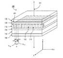
- FIG. 1is a perspective view of an embodiment of an polarizer.
- FIGS. 2A-2Jshow steps in the manufacture of the polarizer shown in FIG. 1 .
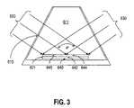
- FIG. 3is a schematic diagram showing exposure of an article in immersion holographic lithography.
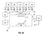
- FIG. 4Ais a schematic diagram of an atomic layer deposition system.
- FIG. 4Bis a cross-sectional view of an embodiment of an article with a nanolaminate film.
- FIG. 5is a flow chart showing steps for forming a nanolaminate using atomic layer deposition.
- FIG. 6is a cross-sectional view of a circular polarizer incorporating a linear polarizer.
- FIG. 7is a cross-sectional view of a polarizing beam splitter.
- FIG. 8is a schematic diagram of a liquid crystal projection display.
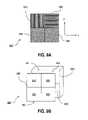
- FIG. 9Ais a diagram of a polarizer that includes a grating array.
- FIG. 9Bis a diagram of a detector assembly including a grating array.
- a linear polarizer 100includes a grating layer 110 and two antireflection films 150 and 160 .
- Linear polarizer 100also includes a substrate 140 , an etch stop layer 130 , and a cap layer 120 .
- Grating layer 110includes elongated portions 111 having a first composition and portions 112 having a different composition. The different compositions have different optical properties for light of wavelength ⁇ .
- Grating layer 110linearly polarizes incident light of wavelength ⁇ propagating along an axis 101 , parallel to the z-axis of the Cartesian coordinate system shown in FIG. 1 .
- linear polarizer 100transmits a relatively large amount of the component of incident light plane-polarized in the x-direction (referred to as “pass” state polarization) while blocking a relatively large amount of the component plane-polarized in the y-direction (referred to as “block” state polarization).
- a layertransmits a relatively large amount of a component of incident light if it transmits about 60% or more of the incident component (e.g., about 80% or more, about 90% or more, about 95% or more, about 98% or more, about 99% or more).
- a layerblocks a relatively large amount of a component of incident light if it blocks about 80% or more of the incident component (e.g., about 90% or more, about 95% or more, about 98% or more, about 99% or more).
- ⁇is between about 150 nm and about 5,000 nm. In certain embodiments, ⁇ corresponds to a wavelength within the visible portion of the electromagnetic spectrum (e.g., from about 400 nm to about 700 nm).
- linear polarizer 100polarizes radiation at more than one wavelength, such as for a continuous band of wavelengths.
- linear polarizer 100can polarize radiation for a band of wavelengths about 50 nm wide or more (e.g., about 100 nm wide or more, about 200 nm wide or more, about 300 nm wide or more).
- linear polarizer 100polarizes radiation, for substantially the entire visible portion of the electromagnetic spectrum (e.g., for ⁇ from about 400 nm to about 700 nm).
- linear polarizer 100can polarize radiation for substantially the entire near infrared portion of the electromagnetic spectrum (e.g., from about 1,200 nm to 2,000 nm).
- linear polarizer 100polarizes radiation for substantially the entire visible and near infrared portions of the electromagnetic spectrum (e.g., from about 400 nm to about 2,000 nm)
- linear polarizer 100polarizes incident radiation propagating parallel to the z-axis
- polarizer 100can polarize radiation at ⁇ for radiation at non-normal angles of incidence (i.e., for radiation incident on linear polarizer 100 propagating at an angle ⁇ with respect to the z-axis, where ⁇ is non-zero).
- linear polarizer 100can polarize radiation incident at more than one angle of incidence, such as for a range of incident angles.
- linear polarizer 100polarizes radiation incident within a cone of incident angles for ⁇ of about 10° or more (e.g., about 15° or more, about 20° or more). Note that for non-normal incidence, the pass state corresponds to light polarized parallel to the x-z plane, while the block state corresponds to light polarized orthogonal to the x-z plane.
- linear polarizer 100blocks a relatively large amount of incident radiation at ⁇ having the block state polarization by reflecting and/or absorbing a relatively large amount of the block state radiation.
- linear polarizer 100can reflect about 80% or more of incident radiation at ⁇ having the block polarization state (e.g., about 90% or more, about 95% or more).
- absorption of the block state radiationis relatively low.
- block state absorptioncan be about 10% or less (e.g., about 5% or less).
- linear polarizer 100absorbs a relatively large amount of the incident radiation at ⁇ having the block polarization state.
- linear polarizer 100can absorb about 30% or more of the block state polarization (e.g., about 40% or more, about 50% or more).
- Linear polarizer 100can have a relatively high extinction ratio, E T , for transmitted light at ⁇ .
- E Textinction ratio
- the extinction ratiorefers to the ratio of pass state intensity at ⁇ to the block state intensity transmitted by linear polarizer 100 .
- E Tcan be, for example, about 30 or more at ⁇ (e.g., about 50 or more, about 100 or more, about 150 or more).
- E Tcan be very high, such as about 1000 or more.
- linear polarizercan have a relatively high extinction ratio, E R , for reflected light at ⁇ .
- E Ris the ratio of the reflected intensity of block state radiation to the reflected intensity of pass state radiation at ⁇ .
- E Rcan be, for example, about 30 or more (e.g., about 50 or more, about 100 or more, about 150 or more).
- both E T and E Rare relatively high.
- elongated portions 111 and 112extend along the y-direction, forming a periodic structure consisting of a series of alternating rows, where adjacent rows have different optical properties.
- the rows corresponding to portions 111have a width ⁇ 111 in the x-direction, while the rows corresponding to portions 112 have a width ⁇ 112 in the x-direction.
- the grating period, ⁇equal to ⁇ 111 + ⁇ 112 , is smaller than ⁇ and as a result light of wavelength ⁇ interacts with grating layer 110 without encountering significant high-order diffraction that can occur when light interacts with periodic structures.
- Grating layer 110is an example of a nanostructured layer.
- ⁇ 111can be about 0.2 ⁇ or less (e.g., about 0.1 ⁇ or less, about 0.05 ⁇ or less, about 0.04 ⁇ or less, about 0.03 ⁇ or less, about 0.02 ⁇ or less, 0.01 ⁇ or less).
- ⁇ 111is about 200 nm or less (e.g., about 150 nm or less, about 100 nm or less, about 80 nm or less, about 70 nm or less, about 60 nm or less, about 50 nm or less, about 40 nm or less, about 30 nm or less).
- ⁇ 112can be about 0.2 ⁇ or less (e.g., about 0.1 ⁇ or less, about 0.05 ⁇ or less, about 0.04 ⁇ or less, about 0.03 ⁇ or less, about 0.02 ⁇ or less, 0.01 ⁇ or less).
- ⁇ 112is about 200 nm or less (e.g., about 150 nm or less, about 100 nm or less, about 80 nm or less, about 70 nm or less, about 60 nm or less, about 50 nm or less, about 40 nm or less, about 30 nm or less).
- ⁇ 111 and ⁇ 112can be the same as each other or different.
- ⁇is less than ⁇ , such as about 0.5 ⁇ or less (e.g., about 0.3 ⁇ or less, about 0.2 ⁇ or less, about 0.1 ⁇ or less, about 0.08 ⁇ or less, about 0.05 ⁇ or less, about 0.04 ⁇ or less, about 0.03 ⁇ or less, about 0.02 ⁇ or less, 0.01 ⁇ or less).
- ⁇is about 500 nm or less (e.g., about 300 nm or less, about 200 nm or less, about 150 nm or less, about 130 nm or less, about 100 nm or less, about 80 nm or less, about 60 nm or less, about 50 nm or less, about 40 nm or less).
- the duty cycle of grating layercan vary as desired. In some embodiments, the duty cycle is less than about 50% (e.g., about 40% or less, about 30% or less, about 20% or less). Alternatively, in certain embodiments, the duty cycle is more than about 50% (e.g., about 60% or more, about 70% or more, about 80% or more).
- grating layer 110is shown as having 19 portions, in general, the number of portions in a grating layer may vary as desired. The number of portions depends on the period, ⁇ , and the area required by the linear polarizer's end use application. In some embodiments, grating layer 110 can have about 50 or more portions (e.g., about 100 or more portions, about 500 or more portions, about 1,000 or more portions, about 5,000 or more portions, about 10,000 or more portions, about 50,000 or more portions, about 100,000 or more portions, about 500,000 more portions).
- portionse.g., about 100 or more portions, about 500 or more portions, about 1,000 or more portions, about 5,000 or more portions, about 10,000 or more portions, about 50,000 or more portions, about 100,000 or more portions, about 500,000 more portions.
- the thickness, d, of grating layer 110 measured along the z-axiscan vary as desired. In general, the thickness of layer 110 is selected based on the refractive indices of portions 111 and 112 and the desired optical properties of grating layer 110 at ⁇ . In some embodiments, d can be about 50 nm or more (e.g., about 75 nm or more, about 100 nm or more, about 125 nm or more, about 150 nm or more, about 200 nm or more, about 250 nm or more, about 300 nm or more, about 400 nm or more, about 500 nm or more, about 1,000 or more, such as about 2,000 nm).
- dcan be about 50 nm or more (e.g., about 75 nm or more, about 100 nm or more, about 125 nm or more, about 150 nm or more, about 200 nm or more, about 250 nm or more, about 300 nm or more, about 400
- the aspect ratio of grating layer thickness, d, to ⁇ 111 and/or d to ⁇ 112can be relatively high.
- d: ⁇ 111 and/or d: ⁇ 112can be about 2:1 or more (e.g., about 3:1 or more, about 4:1 or more, about 5:1 or more, about 8:1 or more, about 10:1 or more).
- portions 111 and 112are selected so that polarizer 100 has desired polarizing properties.
- Portions 111 and/or 112can include inorganic and/or organic materials.
- inorganic materialsinclude metals, semiconductors, and inorganic dielectric materials (e.g., glass).
- organic materialsinclude polymers.
- portions 111 and/or portions 112include one or more dielectric materials, such as dielectric oxides (e.g., metal oxides), fluorides (e.g., metal fluorides), sulphides, and/or nitrides (e.g., metal nitrides).
- oxidesinclude SiO 2 , Al 2 O 3 , Nb 2 O 5 , TiO 2 , ZrO 2 , HfO 2 , SnO 2 , ZnO, ErO 2 , Sc 2 O 3 , and Ta 2 O 5 .
- fluoridesinclude MgF 2 .
- Other examplesinclude ZnS, SiN x , SiO y N x , AlN, TiN, and HfN.
- portions 111 and/or portions 112include a metal, such as Au, Ag, Al, Cr, and Cu. Portions 111 and/or portions 112 can be formed from more than one metal (e.g., portions 111 and/or portions 112 can be formed from a metal alloy).
- portions 111 and 112are typically selected based on their optical properties and their compatibility with the processes used to manufacture polarizer 100 and their compatibility with the materials used to form other layers of polarizer 100 .
- portions 111are composed of a material that is transmissive at ⁇
- portions 112are composed of a material that is non-transmissive at ⁇ .
- a one millimeter thick sample of a transmissive materialtransmits about 80% or more of radiation at ⁇ normally incident thereon (e.g., about 90% or more, about 95% or more, about 98% or more, about 99% or more).
- transmissive materials for visible and infrared wavelengthsinclude various dielectric materials, such as SiO 2 .
- a one millimeter thick sample of a non-transmissive materialtransmits less than about 1% or less of radiation at ⁇ normally incident thereon (e.g., about 0.5% or less, about 0.1% or less, about 0.01% or less, about 0.001% or less).
- Non-transmissive materialsinclude materials that reflect and/or absorb a relatively large amount of radiation at ⁇ .
- Examples of non-transmissive materials for visible and infrared wavelengthsinclude various metals, such as Al, Au, Ag, Cr, and Cu.
- Al and Agare examples of materials that have high reflectance across the visible portion of the electromagnetic spectrum, while Au and Cu have high reflectance for the yellow and red portions of the spectrum, while absorbing relatively more of the shorter visible wavelengths (e.g., the green and blue wavelengths).
- the composition of portions 111 and portions 112have a relatively low absorption at ⁇ , so that grating layer 110 has a relatively low absorption at ⁇ .
- grating layer 110can absorb about 10% or less of radiation at ⁇ propagating along axis 101 (e.g., about 5% or less, about 3% or less, about 2% or less, about 1% or less).
- Portions 111 and/or portions 112can be formed from a single material or from multiple different materials.
- one or both of portions 111 and 112are formed from a nanolaminate material, which refers to materials that are composed of layers of at least two different materials and the layers of at least one of the materials are extremely thin (e.g., between one and about 10 monolayers thick).
- nanolaminate materialshave a locally homogeneous index of refraction that depends on the refractive index of its constituent materials. Varying the amount of each constituent material can vary the refractive index of a nanolaminate.
- nanolaminate portionsinclude portions composed of SiO 2 monolayers and TiO 2 monolayers, SiO 2 mono layers and Ta 2 O 5 mono layers, or Al 2 O 3 mono layers and TiO 2 mono layers
- portions 111 and/or portions 112can include crystalline, semi-crystalline, and/or amorphous portions.
- an amorphous materialis optically isotropic and may transmit radiation better than portions that are partially or mostly crystalline.
- both portions 111 and 112are formed from amorphous materials, such as amorphous dielectric materials (e.g., amorphous TiO 2 or SiO 2 ).
- portions 111are formed from a crystalline or semi-crystalline material (e.g., crystalline or semi-crystalline Si), while portions 112 are formed from an amorphous material (e.g., an amorphous dielectric material, such as TiO 2 or SiO 2 ).
- the structure and composition of grating layer 110is selected based on the desired optical performance of linear polarizer 100 .
- Structural parameters that affect the optical performance of linear polarize 100include, for example, d, ⁇ , ⁇ 111 , and ⁇ 112 .
- varying a single parameteraffects multiple different performance parameters.
- the overall transmission of the polarizer at ⁇can be varied by changing the relative thickness of portions formed from a transmissive material, ⁇ 111 , to the thickness or portions formed from a non-transmissive material, ⁇ 112 .
- the period ⁇ of the grating layershould be shorter than ⁇ , such as about ⁇ /4 or less (e.g., about ⁇ /6 or less, about ⁇ /10 or less).
- ⁇should be shorter than the shortest wavelength in the wavelength band.
- ⁇should be less than about 300 nm, such as about 200 nm or less (e.g., about 150 nm or less, about 130 nm or less, about 110 nm or less, about 100 nm or less, about 90 nm or less, about 80 nm or less).
- the reflectance of grating layer 110can be increased by forming at least some of the portions from a material having a relatively high reflectance at ⁇ .
- the reflectance of the polarizecan also be increased by increasing the relative size of the portions of reflective material relative to the portions of transmissive material.
- a larger duty cyclecan provide increased reflectance at ⁇ .
- the transmission of grating layer 110can be increased by reducing the duty cycle.
- the duty cycleis in the range of about 20% to about 80%.
- E Tcan be increased by increasing the depth of grating layer 110 , d. Increasing d can provide increased E T without substantially reducing the amount of pass state transmission.
- polarizer transmissioncan be increased by forming portion 111 from materials that have a relatively high transmission at ⁇ .
- portions 111can reduce reflection of the pass state radiation.
- portions 111can be formed from a material having a refractive index of about 1.6 or less at 1 (e.g., about 1.55 or less, about 1.5 or less, about 1.45 or less).
- SiO 2is an example of a material with a relatively low refractive index in the visible portion of the electromagnetic spectrum. Reflection can be reduced because the effective refractive index of grating layer 110 is reduced relative to a grating layer where portions 111 are formed from a material having a relatively high refractive index.
- Selecting a material or materials having a relatively low refractive index at ⁇ for any part of polarizer 100 that contact portions 112can improve optical characteristics of the grating layer, such as, for example, E T .
- portions 112should be formed from a material that has a high reflectivity at ⁇ .
- the materialshould have a relatively high reflectivity for all wavelengths in the band.
- Alprovides higher broadband reflectivity for visible wavelengths compared to Au or Cu, for example, which have higher absorption for shorter visible wavelengths.
- substrate 140provides mechanical support to polarizer 100 .
- substrate 140is transparent to light at wavelength ⁇ , transmitting substantially all light impinging thereon at wavelength ⁇ (e.g., about 90% or more, about 95% or more, about 97% or more, about 99% or more, about 99.5% or more).
- substrate 140can be formed from any material compatible with the manufacturing processes used to produce retarder 100 that can support the other layers.
- substrate 140is formed from a glass, such as BK7 (available from Abrisa Corporation), borosilicate glass (e.g., pyrex available from Corning), aluminosilicate glass (e.g., C1737 available from Corning), or quartz/fused silica.
- substrate 140can be formed from a crystalline material, such as a non-linear optical crystal (e.g., LiNbO 3 or a magneto-optical rotator, such as garnett) or a crystalline (or semicrystalline) semiconductor (e.g., Si, InP, or GaAs).
- Substrate 140can also be formed from an inorganic material, such as a polymer (e.g., a plastic).
- Etch stop layer 130is formed from a material resistant to etching processes used to etch the material(s) from which portions 112 are formed (see discussion below).
- the material(s) forming etch stop layer 130should also be compatible with substrate 140 and with the materials forming grating layer 110 .
- Examples of materials that can form etch stop layer 130include HfO 2 , SiO 2 , Ta 2 O 5 , TiO 2 , SiN x , or metals (e.g., Cr, Ti, Ni).
- etch stop layer 130can be varied as desired. Typically, etch stop layer 130 is sufficiently thick to prevent significant etching of substrate 140 , but should not be so thick as to adversely impact the optical performance of polarizer 100 . In some embodiments, etch stop layer is about 500 nm or less (e.g., about 250 nm or less, about 100 nm or less, about 75 nm or less, about 50 nm or less, about 40 nm or less, about 30 nm or less, about 20 nm or less).
- Cap layer 120is typically formed from the same material(s) as portions 111 of grating layer 110 and provides a surface 121 onto which additional layers, such as the layers forming antireflection film 150 , can be deposited.
- Surface 121can be substantially planar.
- Antireflection films 150 and 160can reduce the reflectance of pass state light of wavelength ⁇ impinging on and exiting polarizer 100 .
- Antireflection film 150 and 160generally include one or more layers of different refractive index.
- one or both of antireflection films 150 and 160can be formed from four alternating high and low index layers.
- the high index layerscan be formed from TiO 2 or Ta 2 O 5 and the low index layers can be formed from SiO 2 or MgF 2 .
- the antireflection filmscan be broadband antireflection films or narrowband antireflection films.
- polarizer 100has a reflectance of about 5% or less of light impinging thereon at wavelength ⁇ for pass state polarization (e.g., about 3% or less, about 2% or less, about 1% or less, about 0.5% or less, about 0.2% or less).
- polarizer 100can be prepared as desired.
- FIGS. 2A-2Jshow different phases of an example of a preparation process. Initially, substrate 140 is provided, as shown in FIG. 2A . Surface 141 of substrate 140 can be polished and/or cleaned (e.g., by exposing the substrate to one or more solvents, acids, and/or baking the substrate).
- etch stop layer 130is deposited on surface 141 of substrate 140 .
- the material forming etch stop layer 130can be formed using one of a variety of techniques, including sputtering (e.g., radio frequency sputtering), evaporating (e.g., electron beam evaporation, ion assisted deposition (IAD) electron beam evaporation), or chemical vapor deposition (CVD) such as plasma enhanced CVD (PECVD), ALD, or by oxidization.
- a layer of HfO 2can be deposited on substrate 140 by IAD electron beam evaporation.
- an intermediate layer 210is then deposited on surface 131 of etch stop layer 130 . Portions 112 are etched from intermediate layer 210 , so intermediation layer 210 is formed from the material used for portions 112 .
- the material forming intermediate layer 210can be deposited using one of a variety of techniques, including sputtering (e.g., radio frequency sputtering), evaporating (e.g., election beam evaporation), or chemical vapor deposition (CVD) (e.g., plasma enhanced CVD).
- intermediate layer 210is formed from a metal, such as aluminum.
- Metal layerscan be formed by evaporation (e.g., thermal evaporation), for example.
- metal layersare formed by evaporating the metal onto surface 131 at relatively fast rates, such as about 5 Angstroms per second or more (e.g., about 10 Angstroms per second or more, about 12 Angstroms per second or more, about 15 Angstroms per second or more), for example.
- Fast deposition ratescan improve the purity of the metal layer by reducing the amount of impurities (such as oxygen) that can incorporate into the film as it is deposited.
- the substratecan be cooled prior to and/or during metal deposition.
- the substratecan be cooled to about 0° C. or less (e.g., about ⁇ 20° C. or less, about ⁇ 50° C. or less). Cooling the substrate can increase the size of metal grains formed on the substrate during deposition. It is believed than lower substrate temperature can reduce the kinetic energy of the metal clusters that tend to prevent the clusters from forming larger grains. Larger metal grain size may be beneficial by providing improved optical characteristics, such as higher reflectance compared to metal layers composed of smaller grains. Moreover, grating layers having short periods can be more easily formed from metal layers having larger grain sizes.
- Evaporationcan also be performed under relatively high vacuums, such as vacuums of about 10 ⁇ 6 Torr or less (e.g., about 5 ⁇ 10 ⁇ 7 Torr or less, about 2 ⁇ 10 ⁇ 7 Torr or less).
- High vacuum depositioncan also improve the purity of the metal layer by reducing the amount of impurities (such as oxygen) present in the vicinity of the deposited layer as it is formed, thereby reducing the amount of impurities that are incorporated in the film.
- substrate 140is positioned relatively far from the source of the deposited metal in the deposition chamber (e.g., about 12 inches or more, about 15 inches or more, about 20 inches or more, about 24 inches or more). This can increase the uniformity of the deposited material across surface 131 relative to systems in which the source is positioned closer to the substrate.
- the thickness of intermediate layer 210is selected based on the desired thickness of grating layer 110 .
- Intermediate layer 210is processed to provide portions 112 of grating layer 110 using lithographic techniques.
- portions 112can be formed from intermediate layer 210 using electron beam lithography or photolithography (e.g., using a photomask or using holographic techniques).
- portions 112are formed using nano-imprint lithography.
- nano-imprint lithographyincludes forming a layer 220 of a resist on surface 211 of intermediate layer 210 .
- the resistcan be polymethylmethacrylate (PMMA) or polystyrene (PS), for example.
- a patternis impressed into resist layer 220 using a mold.
- the patterned resist layer 220includes thin portions 221 and thick portions 222 .
- Patterned resist layer 220is then etched (e.g., by oxygen reactive ion etching (RIE)), removing thin portions 221 to expose portions 224 of surface 211 of intermediate layer 210 , as shown in FIG. 2F .
- Thick portions 222are also etched, but are not completely removed. Accordingly, portions 223 of resist remain on surface 211 after etching.
- intermediate layer 210is subsequently etched, forming trenches 212 in intermediate layer 210 .
- the unetched portions of intermediate layer 210correspond to portions 112 of grating layer 110 .
- Intermediate layer 210can be etched using, for example, reactive ion etching, ion beam etching, sputtering etching, chemical assisted ion beam etching (CAIBE), or wet etching.
- the exposed portions of intermediate layer 210are etched down to etch stop layer 130 , which is formed from a material resistant to the etching method. Accordingly, the depth of trenches 212 formed by etching is the same as the thickness of portions 112 .
- Resistcan be removed by rinsing the article in a solvent (e.g., an organic solvent, such as acetone or alcohol), by O 2 plasma ashing, O 2 RIE, or ozone cleaning.
- a solvente.g., an organic solvent, such as acetone or alcohol
- an etch maskis formed on the surface of intermediate layer 210 prior to depositing resist layer 220 .
- Etch masksare provide to prevent etching of layer 210 by the etchant used to remove portions of the resist layer.
- Certain oxide materialse.g., SiO 2
- etchantse.g., reactive ion etchants
- a layer of SiO 2can be used to mask a metal layer from a chlorine-based reactive ion etchant.
- Etch mask layerscan be relatively thin (e.g., about 100 nm or less, 50 nm or less, such as in a range from about 20 nm to about 25 nm).
- Etchingcan be performed using commercially-available equipment, such as a TCP® 9600DFM (available from Lam Research, Fremont, Calif.).
- More than one etch stepcan be used.
- a two-step etchis used.
- An example of a two step etching process for Alis as follows. The first etch is performed using a gas mixture composed of BCL3 (e.g., at about 90 sccm), Cl 2 (e.g., at about 30 sccm), N2 (e.g., at about 10 sccm), He (e.g., at about 10 Torr) for backside cooling.
- the radio frequency (RF) poweris about 500 W and the chamber pressure about 5 mtorr.
- the second etchis performed using Cl 2 (e.g., at about 56 sccm), HCl (e.g., at about 14 sccm), N 2 (e.g., at about 35 sccm), H 2 (e.g., at about 10 Torr) for back side cooling.
- the RF poweris about 300 W and the chamber pressure is about 7 mtorr.
- the first etching timecan be about 4 seconds and the second etching time can be about 15 seconds.
- a post-etching passivation stepcan be employed to provide a passivation layer on the surface of the etched layer.
- Post-etching passivationcan be done, for example, by exposing the etched layer to an oxidant to produce an oxide layer at the surface of the etched layer.
- Post-etch passivation of an etched Al layerfor example, can be performed by exposing the etched layer to water vapor at an elevated temperature (e.g., at about 200° C. or more, about 250° C. or more, about 300° C. or more).
- materialis deposited onto the article, filling trenches 212 and forming cap layer 120 .
- the filled trenchescorrespond to portions 111 of grating layer 110 .
- Materialcan be deposited onto the article in a variety of ways, including sputtering, electron beam evaporation, CVD (e.g., high density CVD) or atomic layer deposition (ALD). Note that where cap layer 120 is formed and trenches 212 are filled during the same deposition step, portions 111 and cap layer 120 are formed from a continuous portion of material.
- antireflection films 150 and 160are deposited onto surface 121 of cap layer 120 and surface 142 of substrate 140 , respectively.
- Materials forming the antireflection filmscan be deposited onto the article by sputtering, electron beam evaporation, or ALD, for example.
- multiple polarizerscan be prepared simultaneously by forming a relatively large grating layer on a single substrate, which is then diced into individual units.
- a grating layercan be formed on a substrate that has a single-side surface area about 10 square inches or more (e.g., a four inch, six inch, or eight inch diameter substrate). After forming the grating layer, the substrate can be diced into multiple units of smaller size (e.g., having a single-side surface area of about one square inch or less).
- holographic lithography techniquescan be used to form a pattern in a layer of resist material on intermediate layer 210 .
- a photosensitive resist layeris exposed to an interference pattern formed by overlapping two or more coherence beams of radiation, usually derived from a laser light source.
- the varying light intensity of the interference patternis transferred to the resist material, which can be developed after exposure to provide a patterned resist layer.
- Holographic lithographycan be used to generate a period intensity pattern by interfering two coherent beams of similar intensity.
- the techniqueis particularly versatile as the period of the intensity pattern can be varied by varying the angle at which the two beams interfere.
- interference patterns having relatively short periodscan be formed by selecting a light source with a relatively short wavelength (e.g., an argon laser having output at 351 nm).
- the interference pattern periodcan be reduced by interfering the two beams at relatively large angles (e.g., ⁇ about 45 degrees or more).
- the resistcan be exposed to two 351 nm beams with ⁇ at about 61 degrees to provide a grating having a period of about 200 nm.
- holographic lithographycan be performed while immersing the substrate and resist in a medium having a refractive index higher than the refractive index of air.
- the resist surfacecan be immersed in a liquid such as water (which has a refractive index of about 1.33) or an organic liquid (e.g., glycerin, which has a refractive index of about 1.5)
- immersion holographic lithographycan be performed by immersing an article 601 in a container 610 filled with a liquid 611 , such as water or glycerin, and exposing the article to an interference pattern while it is immersed.
- the interference patternis formed by interfering coherent beams 620 and 630 at angle ⁇ .
- the walls of container 610can be oriented so that beams 620 and 630 are substantially normally incident. Alternatively, or additionally, certain walls of container 610 can include an antireflection coating to reduce reflection of beams 620 and 630 .
- the beamsare expanded to provide an interference pattern sufficiently large to expose article 601 in a single exposure.
- the beamscan be expanded to have a diameter of several inches (e.g., about 4 inches or more, about 6 inches or more, about 8 inches or more).
- article 601includes a substrate layer 640 , an intermediate layer 642 disposed on substrate layer 640 , and a photoresist layer 644 disposed on intermediate layer 642 .
- a surface 645 of photoresist layer 644is exposed to the interference pattern.
- portions 111 of grating layer 110 , cap layer 120 , and/or one or both of antireflection films 150 and 160are prepared using atomic layer deposition (ALD).
- ALDatomic layer deposition
- an ALD system 300is used to fill trenches 212 of an intermediate article 301 (composed of substrate 140 , cap layer 130 , and portions 112 ) with a nanolaminate multilayer film 4001 , forming portions 111 and cap layer 120 .
- Deposition of nanolaminate multilayer film 4001occurs monolayer by monolayer, providing substantial control over the composition and thickness of the films.
- vapors of a precursorare introduced into the chamber and are adsorbed onto exposed surfaces of portions 112 , etch stop layer surface 131 or previously deposited monolayers adjacent these surfaces.
- a reactantis introduced into the chamber that reacts chemically with the adsorbed precursor, forming a monolayer of a desired material.
- the self-limiting nature of the chemical reaction on the surfacecan provide precise control of film thickness and large-area uniformity of the deposited layer.
- the non-directional adsorption of precursor onto each exposed surfaceprovides for uniform deposition of material onto the exposed surfaces, regardless of the orientation of the surface relative to chamber 110 . Accordingly, the layers of the nanolaminate film conform to the shape of the trenches of intermediate article 301 .
- ALD system 300includes a reaction chamber 310 , which is connected to sources 350 , 360 , 370 , 380 , and 390 via a manifold 330 .
- Sources 350 , 360 , 370 , 380 , and 390are connected to manifold 330 via supply lines 351 , 361 , 371 , 381 , and 391 , respectively.
- Valves 352 , 362 , 372 , 382 , and 392regulate the flow of gases from sources 350 , 360 , 370 , 380 , and 390 , respectively.
- Sources 350 and 380contain a first and second precursor, respectively, while sources 360 and 390 include a first reagent and second reagent, respectively.
- Source 370contains a carrier gas, which is constantly flowed through chamber 310 during the deposition process transporting precursors and reagents to article 301 , while transporting reaction byproducts away from the substrate. Precursors and reagents are introduced into chamber 310 by mixing with the carrier gas in manifold 330 . Gases are exhausted from chamber 310 via an exit port 345 . A pump 340 exhausts gases from chamber 310 via an exit port 345 . Pump 340 is connected to exit port 345 via a tube 346 .
- ALD system 300includes a temperature controller 395 , which controls the temperature of chamber 310 .
- temperature controller 395elevates the temperature of article 301 above room temperature.
- the temperatureshould be sufficiently high to facilitate a rapid reaction between precursors and reagents, but should not damage the substrate.
- the temperature of article 301can be about 500° C. or less (e.g., about 400° C. or less, about 300° C. or less, about 200° C. or less, about 150° C. or less, about 125° C. or less, about 100° C. or less).
- the temperatureshould not vary significantly between different portions of article 301 .
- Large temperature variationscan cause variations in the reaction rate between the precursors and reagents at different portions of the substrate, which can cause variations in the thickness and/or morphology of the deposited layers.
- the temperature between different portions of the deposition surfacescan vary by about 40° C. or less (e.g., about 30° C. or less, about 20° C. or less, about 10° C. or less, about 5° C. or less).
- Deposition process parametersare controlled and synchronized by an electronic controller 399 .
- Electronic controller 399is in communication with temperature controller 395 ; pump 340 ; and valves 352 , 362 , 372 , 382 , and 392 .
- Electronic controller 399also includes a user interface, from which an operator can set deposition process parameters, monitor the deposition process, and otherwise interact with system 300 .
- the ALD processis started ( 410 ) when system 300 introduces the first precursor from source 350 into chamber 310 by mixing it with carrier gas from source 370 ( 420 ). A monolayer of the first precursor is adsorbed onto exposed surfaces of article 301 , and residual precursor is purged from chamber 310 by the continuous flow of carrier gas through the chamber ( 430 ).
- the systemintroduces a first reagent from source 360 into chamber 310 via manifold 330 ( 440 ).
- the first reagentreacts with the monolayer of the first precursor, forming a monolayer of the first material.
- the flow of carrier gaspurges residual reagent from the chamber ( 450 ). Steps 420 through 460 are repeated until the layer of the first material reaches a desired thickness ( 460 ).
- the processceases once the layer of first material reaches the desired thickness ( 470 ).
- the systemintroduces a second precursor into chamber 310 through manifold 330 ( 380 ).
- a monolayer of the second precursoris adsorbed onto the exposed surfaces of the deposited layer of first material and carrier gas purges the chamber of residual precursor ( 490 ).
- the systemthen introduces the second reagent from source 380 into chamber 310 via manifold 330 .
- the second reagentreacts with the monolayer of the second precursor, forming a monolayer of the second material ( 500 ).
- Flow of carrier gas through the chamberpurges residual reagent ( 510 ). Steps 580 through 510 are repeated until the layer of the second material reaches a desired thickness ( 520 ).
- Additional layers of the first and second materialsare deposited by repeating steps 520 through 530 .
- the processterminates ( 540 ), and the coated article is removed from chamber 310 .
- the precursoris introduced into the chamber before the reagent during each cycle in the process described above, in other examples the reagent can be introduced before the precursor.
- the order in which the precursor and reagent are introducedcan be selected based on their interactions with the exposed surfaces. For example, where the bonding energy between the precursor and the surface is higher than the bonding energy between the reagent and the surface, the precursor can be introduced before the reagent. Alternatively, if the binding energy of the reagent is higher, the reagent can be introduced before the precursor.
- each monolayergenerally depends on a number of factors.
- the thickness of each monolayercan depend on the type of material being deposited. Materials composed of larger molecules may result in thicker monolayers compared to materials composed of smaller molecules.
- the temperature of the articlecan also affect the monolayer thickness. For example, for some precursors, a higher temperate can reduce adsorption of a precursor onto a surface during a deposition cycle, resulting in a thinner monolayer than would be formed if the substrate temperature were lower.
- monolayer thicknesscan also affect monolayer thickness.
- monolayers of a materialcan be deposited with a particular precursor, but with different reagents, resulting in different monolayer thickness for each combination.
- monolayers of a material formed from different precursorscan result in different monolayer thickness for the different precursors.
- Examples of other factors which may affect monolayer thicknessinclude purge duration, residence time of the precursor at the coated surface, pressure in the reactor, physical geometry of the reactor, and possible effects from the byproducts on the deposited material.
- An example of where the byproducts affect the film thicknessare where a byproduct etches the deposited material.
- HClis a byproduct when depositing TiO 2 using a TiCl 4 precursor and water as a reagent. HCl can etch the deposited TiO 2 before it is exhausted.
- Etchingwill reduce the thickness of the deposited monolayer, and can result in a varying monolayer thickness across the substrate if certain portions of the substrate are exposed to HCl longer than other portions (e.g., portions of the substrate closer to the exhaust may be exposed to byproducts longer than portions of the substrate further from the exhaust).
- monolayer thicknessis between about 0.1 nm and about five nm.
- the thickness of one or more of the deposited monolayerscan be about 0.2 nm or more (e.g., about 0.3 nm or more, about 0.5 nm or more).
- the thickness of one or more of the deposited monolayerscan be about three nm or less (e.g., about two nm, about one nm or less, about 0.8 nm or less, about 0.5 nm or less).
- the average deposited monolayer thicknessmay be determined by depositing a preset number of monolayers on a substrate to provide a layer of a material. Subsequently, the thickness of the deposited layer is measured (e.g., by ellipsometry, electron microscopy, or some other method). The average deposited monolayer thickness can then be determined as the measured layer thickness divided by the number of deposition cycles.
- the average deposited monolayer thicknessmay correspond to a theoretical monolayer thickness.
- the theoretical monolayer thicknessrefers to a characteristic dimension of a molecule composing the monolayer, which can be calculated from the material's bulk density and the molecules molecular weight. For example, an estimate of the monolayer thickness for SiO 2 is ⁇ 0.37 nm. The thickness is estimated as the cube root of a formula unit of amorphous SiO 2 with density of 2.0 grams per cubic centimeter.
- average deposited monolayer thicknesscan correspond to a fraction of a theoretical monolayer thickness (e.g., about 0.2 of the theoretical monolayer thickness, about 0.3 of the theoretical monolayer thickness, about 0.4 of the theoretical monolayer thickness, about 0.5 of the theoretical monolayer thickness, about 0.6 of the theoretical monolayer thickness, about 0.7 of the theoretical monolayer thickness, about 0.8 of the theoretical monolayer thickness, about 0.9 of the theoretical monolayer thickness).
- a theoretical monolayer thicknesse.g., about 0.2 of the theoretical monolayer thickness, about 0.3 of the theoretical monolayer thickness, about 0.4 of the theoretical monolayer thickness, about 0.5 of the theoretical monolayer thickness, about 0.6 of the theoretical monolayer thickness, about 0.7 of the theoretical monolayer thickness, about 0.8 of the theoretical monolayer thickness, about 0.9 of the theoretical monolayer thickness.
- the average deposited monolayer thicknesscan correspond to more than one theoretical monolayer thickness up to about 30 times the theoretical monolayer thickness (e.g., about twice or more than the theoretical monolayer thickness, about three time or more than the theoretical monolayer thickness, about five times or more than the theoretical monolayer thickness, about eight times or more than the theoretical monolayer thickness, about 10 times or more than the theoretical monolayer thickness, about 20 times or more than the theoretical monolayer thickness).
- the theoretical monolayer thicknesse.g., about twice or more than the theoretical monolayer thickness, about three time or more than the theoretical monolayer thickness, about five times or more than the theoretical monolayer thickness, about eight times or more than the theoretical monolayer thickness, about 10 times or more than the theoretical monolayer thickness, about 20 times or more than the theoretical monolayer thickness.
- the pressure in chamber 310can be maintained at substantially constant pressure, or can vary. Controlling the flow rate of carrier gas through the chamber generally controls the pressure. In general, the pressure should be sufficiently high to allow the precursor to saturate the surface with chemisorbed species, the reagent to react completely with the surface species left by the precursor and leave behind reactive sites for the next cycle of the precursor. If the chamber pressure is too low, which may occur if the dosing of precursor and/or reagent is too low, and/or if the pump rate is too high, the surfaces may not be saturated by the precursors and the reactions may not be self limited. This can result in an uneven thickness in the deposited layers.
- the chamber pressureshould not be so high as to hinder the removal of the reaction products generated by the reaction of the precursor and reagent. Residual byproducts may interfere with the saturation of the surface when the next dose of precursor is introduced into the chamber.
- the chamber pressureis maintained between about 0.01 Torr and about 100 Torr (e.g., between about 0.1 Torr and about 20 Torr, between about 0.5 Torr and 10 Torr, such as about 1 Torr).
- the amount of precursor and/or reagent introduced during each cyclecan be selected according to the size of the chamber, the area of the exposed substrate surfaces, and/or the chamber pressure.
- the amount of precursor and/or reagent introduced during each cyclecan be determined empirically.
- the amount of precursor and/or reagent introduced during each cyclecan be controlled by the timing of the opening and closing of valves 352 , 362 , 382 , and 392 .
- the amount of precursor or reagent introducedcorresponds to the amount of time each valve is open each cycle.
- the valvesshould open for sufficiently long to introduce enough precursor to provide adequate monolayer coverage of the substrate surfaces.
- the amount of reagent introduced during each cycleshould be sufficient to react with substantially all precursor deposited on the exposed surfaces. Introducing more precursor and/or reagent than is necessary can extend the cycle time and/or waste precursor and/or reagent.
- the precursor dosecorresponds to opening the appropriate valve for between about 0.1 seconds and about five seconds each cycle (e.g., about 0.2 seconds or more, about 0.3 seconds or more, about 0.4 seconds or more, about 0.5 seconds or more, about 0.6 seconds or more, about 0.8 seconds or more, about one second or more).
- the reagent dosecan correspond to opening the appropriate valve for between about 0.1 seconds and about five seconds each cycle (e.g., about 0.2 seconds or more, about 0.3 seconds or more, about 0.4 seconds or more, about 0.5 seconds or more, about 0.6 seconds or more, about 0.8 seconds or more, about one second or more).
- the time between precursor and reagent dosescorresponds to the purge.
- the duration of each purgeshould be sufficiently long to remove residual precursor or reagent from the chamber, but if it is longer than this it can increase the cycle time without benefit.
- the duration of different purges in each cyclecan be the same or can vary.
- the duration of a purgeis about 0.1 seconds or more (e.g., about 0.2 seconds or more, about 0.3 seconds or more, about 0.4 seconds or more, about 0.5 seconds or more, about 0.6 seconds or more, about 0.8 seconds or more, about one second or more, about 1.5 seconds or more, about two seconds or more).
- the duration of a purgeis about 10 seconds or less (e.g., about eight seconds or less, about five seconds or less, about four seconds or less, about three seconds or less).
- the time between introducing successive doses of precursorcorresponds to the cycle time.
- the cycle timecan be the same or different for cycles depositing monolayers of different materials. Moreover, the cycle time can be the same or different for cycles depositing monolayers of the same material, but using different precursors and/or different reagents. In some embodiments, the cycle time can be about 20 seconds or less (e.g., about 15 seconds or less, about 12 seconds or less, about 10 seconds or less, about 8 seconds or less, about 7 seconds or less, about 6 seconds or less, about 5 seconds or less, about 4 seconds or less, about 3 seconds or less). Reducing the cycle time can reduce the time of the deposition process.
- the precursorsare generally selected to be compatible with the ALD process, and to provide the desired deposition materials upon reaction with a reagent.
- the precursors and materialsshould be compatible with the material on which they are deposited (e.g., with the substrate material or the material forming the previously deposited layer).
- Examples of precursorsinclude chlorides (e.g., metal chlorides), such as TiCl 4 , SiCl 4 , SiH 2 Cl 2 , TaCl 3 , HfCl 4 , InCl 3 and AlCl 3 .
- organic compoundscan be used as a precursor (e.g., Ti-ethaOxide, Ta-ethaOxide, Nb-ethaOxide).
- organic compound precursoris (CH 3 ) 3 Al.
- suitable precursorsinclude Tris(tert-butoxy), Tris(tert-pentoxy) silanol, or tetraethoxysilane (TEOS).
- the reagentsare also generally selected to be compatible with the ALD process, and are selected based on the chemistry of the precursor and material.
- the reagentcan be an oxidizing agent.
- suitable oxidizing agentsinclude water, hydrogen peroxide, oxygen, ozone, (CH 3 ) 3 Al, and various alcohols (e.g., Ethyl alcohol CH 3 OH).
- Waterfor example, is a suitable reagent for oxidizing precursors such as TiCl 4 to obtain TiO 2 , AlCl 3 to obtain Al 2 O 3 , and Ta-ethaoxide to obtain Ta 2 O 5 , Nb-ethaoxide to obtain Nb 2 O 5 , HfCl 4 to obtain HfO 2 , ZrCl 4 to obtain ZrO 2 , and InCl 3 to obtain In 2 O 3 .
- HClis produced as a byproduct.
- (CH 3 ) 3 Alcan be used to oxidize silanol to provide SiO 2 .
- linear polarizer 100shows a specific configuration of different layers
- other embodimentscan include additional or fewer layers.
- polarizersneed not include one or both of antireflection films 150 and 160 .
- polarizerscan include additional antireflection films (e.g., between substrate layer 140 and etch stop layer 130 ).
- Embodimentscan also include protective layers, such as hardcoat layers (e.g., hardcoat polymers) on one or both of antireflection films 150 and 160 .
- polarizersneed not include a cap layer.
- the cap layerwhich forms while filling trenches between portions 112 , can be removed once portions 111 are formed. The cap layer can be removed by, e.g., chemical mechanical polishing or etching.
- polarizershave been described that include a grating layer that has a rectangular grating profile, other embodiments are also possible.
- the grating layerhave a curved profile, such as a sinusoidal profile.
- the grating layercan have a triangular, sawtooth profile, or trapezoidal profile.
- the grating period in the grating layers of polarizershas been described as constant, in certain embodiments the grating period may vary. In some embodiments, portions of grating layers can be non-periodically arranged.
- a linear polarizercan include regions where the portions of the grating layer are oriented along different directions compared to other regions.
- a polarizer 900include a grating layer that has four different grating regions, 910 , 920 , 930 , and 940 , in which the grating portions are aligned along different directions, forming a grating array.
- the pass and block states for each regiondepend on the orientation of the grating portions in that region, the pass and block states are different for regions having different orientation.
- grating arrayscan include as many regions as desired.
- grating arrayscan include several hundred or thousands of regions (e.g., about 500 or more regions, about 1,000 or more regions, about 5,000 or more regions, about 10,000 or more regions).
- grating arrayscan include regions corresponding to standard graphics array (GA) resolutions (e.g., VGA 640 ⁇ 480, XGA 1024 ⁇ 768, SXGA 1280 ⁇ 1024, UXGA 1600 ⁇ 1200 WXGA 1366 ⁇ 768).
- GAgraphics array
- Two or more regions in a grating arraycan have grating layers having the same orientation.
- grating orientationsform a repeated pattern.
- the period and/or duty cycle of each region in a grating arraycan be the same or different.
- Polarizers that include more than one grating regioncan be prepared by the techniques discussed previously. For example, single or multi-exposure photolithographic methods can be used. Grating arrays can be formed using single step exposures by using a lithography mask that has a pattern corresponding to the grating array. Multiple exposure methods include holographic lithography, where the orientation of the substrate and the interference pattern are changed for each exposure. Pre-exposed regions are masked for subsequent exposures.
- Imprint lithographycan also be used to form grating arrays by using mold that has the corresponding grating array pattern.
- Polarizerssuch as those described herein can be incorporated into optical devices, including passive optical devices (e.g., polarizing devices) and active optical devices (e.g., liquid crystal displays). Polarizers can be integrated into the device, providing a monolithic device, or can be arranged separately from other components of the device.
- passive optical devicese.g., polarizing devices
- active optical devicese.g., liquid crystal displays
- Circular polarizer 660includes a linear polarizer 670 and a quarter-waveplate 680 .
- Linear polarizer 670linearly polarizes radiation incident on circular polarizer 660 propagating along axis 661 having wavelength ⁇ .
- Quarter-waveplate 680then retards the linearly polarized light, providing circularly polarized light exiting polarizer 660 .
- the ellipticity of the exiting lightcan vary as desired by choosing waveplates with varying amounts of retardation instead of quarter-waveplate 680 to provide a desired amount of retardation.
- linear polarizerscan be used as a polarizing beam splitter 700 .
- Polarizing beam splitterstypically reflect (e.g., specularly reflect) a relatively large amount of incident block state radiation while transmitting a relatively large amount of the incident pass state radiation.
- PBS 700is positioned with respect to radiation propagating parallel to axis 710 , so that the radiation is incident non-normally on the surface of the PBS.
- PBS 700specularly reflects the incident block state radiation, which propagates away from the PBS in direction 722 .
- PBS 700transmits a relatively large amount of incident pass state radiation, which propagates in direction 720 . Accordingly, PBS 700 provides two beams of orthogonally-polarized radiation.
- Polarizing beam splitterscan be used in projection displays.
- a PBS 810 that includes a linear polarizeris included in a liquid crystal projection display 800 .
- Display 800also includes a broadband light source 830 , beam shaping optics 860 , a reflective liquid crystal display panel 820 , and projection optics 840 .
- Display 800is configured to project an image generated by panel 820 onto a projection screen 850 .
- Display 800operates as follows. Broadband light source 830 emits radiation 801 that is collimated by beam shaping optics 860 and directed towards polarizing beam splitter 810 as a substantially collimated beam 802 .
- beam shaping optics 860include one or more lenses and one or more apertures that gather divergent radiation from source 830 to provide substantially collimated beam 802 .
- beam shaping optics 860can include a polarizing element that linearly polarizes the radiation so that beam 802 includes mainly block state radiation.
- PBS 810reflects the block state component of beam 802 towards panel 820 .
- Panel 820spatially modulates the polarization of incident beam 803 , transforming the polarization state of some of the incident radiation, while leaving the polarization state of some of the incident radiation substantially unchanged.
- certain portions of reflected beam 803have pass state polarization.
- Reflected beam 803returns to PBS 810 where the portions of the beam having pass state polarization are transmitted, while the rest is blocked by the PBS.
- the transmitted radiationshown as beam 804 , propagates to projection optics 804 , which projects radiation, indicated by 805 , out onto screen 850 where it forms an image.
- Projection optics 840conventionally includes one or more lens elements and/or other passive optical components that image panel 820 to screen 850 .
- the imageis typically magnified substantially, so that a relatively small panel can be used to provide a relatively large image that can be viewed by a suitably situated observer.
- grating arrayssuch as polarizer 900
- a detector array 950can be used as polarization analyzers with a detector array 950 to provide a detector assembly 999 capable of simultaneously sampling different polarization components of an incident beam.
- Detector array 950includes elements 951 , 952 , 953 , and 954 that correspond to regions 910 , 920 , 930 , and 940 of polarizer 900 . Because each region of polarizer 900 has its pass state oriented differently to the other regions, each detector element in detector array 950 measures the intensity of a different polarization component.
- the grating arraycan be formed directly on the detector elements.
- polarizer 900can be affixed to detector 950 (e.g., using an adhesive).
- detector assembly 999can be used in a polarimeter to measure the polarization state (e.g., the Stokes parameters) of incident light by a single measurement at each detector element.
- Additional componentssuch as a retarder (e.g., a retarder array), such as a quarter wave plate or quarter wave plate array, and/or a polarizer (e.g., another polarizer array) can be integrated with polarizer 900 to provide a compact polarimeter assembly.
- Retarders and/or polarizerscan be integrated with polarizer 900 using the techniques disclosed herein and the techniques disclosed in U.S. patent application Ser. No. 10/866,416, entitled “OPTICAL FILMS AND METHODS OF MAKING THE SAME,” filed on Jun. 11, 2004.
- Such a polarimeteris referred to as a wavefront division polarimeter because it divides up an incident wavefront into different components and samples a different polarization components for each component.
- Polarimeter arrayscan also be formed using multiple detector assemblies.
- the detector assembliescan be integrated into a single component.
- the detector arrays corresponding to each detector assemblycan be formed on the same substrate.
- Polarimeter arrayscan be used in imaging applications.
- an optical isolatorcan include a polarizer formed directly on a magneto-optic or electro-optic component (such as a garnet crystal) using the techniques described above.
Landscapes
- Physics & Mathematics (AREA)
- General Physics & Mathematics (AREA)
- Optics & Photonics (AREA)
- Engineering & Computer Science (AREA)
- Manufacturing & Machinery (AREA)
- Health & Medical Sciences (AREA)
- Ophthalmology & Optometry (AREA)
- Mechanical Engineering (AREA)
- Polarising Elements (AREA)
- Manufacture Of Macromolecular Shaped Articles (AREA)
Abstract
Description
where λbis the wavelength of the interfering radiation, n is the refractive index of the medium in which the beams interfere, and φ is half the angle subtended by the interfering beams. Since Γ is proportional to λb, interference patterns having relatively short periods (e.g., about 300 nm or less) can be formed by selecting a light source with a relatively short wavelength (e.g., an argon laser having output at 351 nm). Furthermore, the interference pattern period can be reduced by interfering the two beams at relatively large angles (e.g., φ about 45 degrees or more). For example, the resist can be exposed to two 351 nm beams with φ at about 61 degrees to provide a grating having a period of about 200 nm.
Claims (5)
Priority Applications (6)
| Application Number | Priority Date | Filing Date | Title |
|---|---|---|---|
| US11/139,954US7670758B2 (en) | 2004-04-15 | 2005-05-27 | Optical films and methods of making the same |
| KR1020077000725AKR20070052263A (en) | 2004-06-11 | 2005-06-07 | Optical film and method of manufacturing same |
| EP05757327AEP1791653A4 (en) | 2004-06-11 | 2005-06-07 | OPTICAL FILMS AND METHODS OF PRODUCING THEM |
| PCT/US2005/019864WO2005123277A2 (en) | 2004-06-11 | 2005-06-07 | Optical films and methods of making the same |
| JP2007527628AJP4778969B2 (en) | 2004-06-11 | 2005-06-07 | Optical film and method of manufacturing optical film |
| US12/692,193US8808972B2 (en) | 2004-04-15 | 2010-01-22 | Optical films and methods of making the same |
Applications Claiming Priority (3)
| Application Number | Priority Date | Filing Date | Title |
|---|---|---|---|
| US56289004P | 2004-04-15 | 2004-04-15 | |
| US10/866,416US20050275944A1 (en) | 2004-06-11 | 2004-06-11 | Optical films and methods of making the same |
| US11/139,954US7670758B2 (en) | 2004-04-15 | 2005-05-27 | Optical films and methods of making the same |
Related Parent Applications (1)
| Application Number | Title | Priority Date | Filing Date |
|---|---|---|---|
| US10/866,416Continuation-In-PartUS20050275944A1 (en) | 2004-04-15 | 2004-06-11 | Optical films and methods of making the same |
Related Child Applications (1)
| Application Number | Title | Priority Date | Filing Date |
|---|---|---|---|
| US12/692,193ContinuationUS8808972B2 (en) | 2004-04-15 | 2010-01-22 | Optical films and methods of making the same |
Publications (2)
| Publication Number | Publication Date |
|---|---|
| US20050277063A1 US20050277063A1 (en) | 2005-12-15 |
| US7670758B2true US7670758B2 (en) | 2010-03-02 |
Family
ID=35510294
Family Applications (2)
| Application Number | Title | Priority Date | Filing Date |
|---|---|---|---|
| US11/139,954Expired - LifetimeUS7670758B2 (en) | 2004-04-15 | 2005-05-27 | Optical films and methods of making the same |
| US12/692,193Expired - LifetimeUS8808972B2 (en) | 2004-04-15 | 2010-01-22 | Optical films and methods of making the same |
Family Applications After (1)
| Application Number | Title | Priority Date | Filing Date |
|---|---|---|---|
| US12/692,193Expired - LifetimeUS8808972B2 (en) | 2004-04-15 | 2010-01-22 | Optical films and methods of making the same |
Country Status (4)
| Country | Link |
|---|---|
| US (2) | US7670758B2 (en) |
| EP (1) | EP1791653A4 (en) |
| KR (1) | KR20070052263A (en) |
| WO (1) | WO2005123277A2 (en) |
Cited By (29)
| Publication number | Priority date | Publication date | Assignee | Title |
|---|---|---|---|---|
| US20080055723A1 (en)* | 2006-08-31 | 2008-03-06 | Eric Gardner | Durable, Inorganic, Absorptive, Ultra-Violet, Grid Polarizer |
| US20080225251A1 (en)* | 2005-09-30 | 2008-09-18 | Holmes Steven J | Immersion optical lithography system having protective optical coating |
| US20080259976A1 (en)* | 2005-11-30 | 2008-10-23 | The Governors Of The University Of Alberta | Organic Columnar Thin Films |
| US20080278811A1 (en)* | 2004-12-06 | 2008-11-13 | Perkins Raymond T | Selectively Absorptive Wire-Grid Polarizer |
| US20090015794A1 (en)* | 2007-07-11 | 2009-01-15 | Seiko Epson Corporation | Polarization Conversion Unit, Polarization Conversion Device, and Projector |
| US20090066885A1 (en)* | 2007-09-12 | 2009-03-12 | Seiko Epson Corporation | Polarization element, method for manufacturing the same, liquid crystal device, and electronic apparatus |
| US20090169735A1 (en)* | 2006-06-01 | 2009-07-02 | Park In Sung | Manufacturing method of photonic crystal |
| US20100014808A1 (en)* | 2008-06-05 | 2010-01-21 | Colorado School Of Mines | Hybrid dielectric/surface plasmon polariton waveguide with grating coupling |
| US20100265571A1 (en)* | 2004-04-15 | 2010-10-21 | Jian Jim Wang | Optical films and methods of making the same |
| US20110187917A1 (en)* | 2005-01-12 | 2011-08-04 | Canon Kabushiki Kaisha | Optical device |
| US20120168889A1 (en)* | 2011-01-05 | 2012-07-05 | Sony Corporation | Manufacturing method of solid-state imaging device and solid-state imaging device |
| US8248696B2 (en) | 2009-06-25 | 2012-08-21 | Moxtek, Inc. | Nano fractal diffuser |
| US20120305523A1 (en)* | 2011-06-06 | 2012-12-06 | Primal Fernando | Polarizer Devices and Processes of Manufacture |
| US20130120840A1 (en)* | 2011-06-28 | 2013-05-16 | Colorado School Of Mines | Spectroscopic polarimeter |
| US8611007B2 (en) | 2010-09-21 | 2013-12-17 | Moxtek, Inc. | Fine pitch wire grid polarizer |
| US8765360B2 (en) | 2004-04-15 | 2014-07-01 | Polarization Solutions, Llc | Optical films and methods of making the same |
| US8873144B2 (en) | 2011-05-17 | 2014-10-28 | Moxtek, Inc. | Wire grid polarizer with multiple functionality sections |
| US20140354910A1 (en)* | 2013-05-29 | 2014-12-04 | Samsung Electronics Co., Ltd. | Wire grid polarizer, and liquid crystal display panel and liquid crystal display device including the same |
| US8913321B2 (en) | 2010-09-21 | 2014-12-16 | Moxtek, Inc. | Fine pitch grid polarizer |
| US8913320B2 (en) | 2011-05-17 | 2014-12-16 | Moxtek, Inc. | Wire grid polarizer with bordered sections |
| US8922890B2 (en) | 2012-03-21 | 2014-12-30 | Moxtek, Inc. | Polarizer edge rib modification |
| US20150036991A1 (en)* | 2013-08-05 | 2015-02-05 | Taiwan Semiconductor Manufacturing Company, Ltd. | Method of making a metal grating in a waveguide and device formed |
| US9229137B2 (en) | 2013-10-02 | 2016-01-05 | Samsung Display Co., Ltd. | Wire grid polarizer comprising transparent particles, display device including the same, and method of fabricating the wire grid polarizer |
| US9329316B2 (en) | 2013-08-27 | 2016-05-03 | Samsung Electronics Co., Ltd. | Wire grid polarizer and liquid crystal display panel and liquid crystal display device having the same |
| US9348076B2 (en) | 2013-10-24 | 2016-05-24 | Moxtek, Inc. | Polarizer with variable inter-wire distance |
| US20180143359A1 (en)* | 2016-11-21 | 2018-05-24 | Stmicroelectronics (Research & Development) Limited | Wafer level microstructures for an optical lens |
| US20220075109A1 (en)* | 2019-01-31 | 2022-03-10 | Facebook Technologies, Llc | Duty cycle range increase for waveguide combiners |
| US11391957B2 (en) | 2018-10-29 | 2022-07-19 | Stmicroelectronics (Research & Development) Limited | Embedded transmissive diffractive optical elements |
| US11754758B2 (en) | 2016-11-21 | 2023-09-12 | Stmicroelectronics (Crolles 2) Sas | Optical diffuser and its method of manufacture |
Families Citing this family (51)
| Publication number | Priority date | Publication date | Assignee | Title |
|---|---|---|---|---|
| WO2006007868A1 (en)* | 2004-07-22 | 2006-01-26 | Pirelli & C. S.P.A. | Integrated wavelength selective grating-based filter |
| TWI248859B (en)* | 2004-11-24 | 2006-02-11 | Ind Tech Res Inst | Manufacture of mold core used in nanoimprint |
| US7800823B2 (en) | 2004-12-06 | 2010-09-21 | Moxtek, Inc. | Polarization device to polarize and further control light |
| US7570424B2 (en) | 2004-12-06 | 2009-08-04 | Moxtek, Inc. | Multilayer wire-grid polarizer |
| US7630133B2 (en) | 2004-12-06 | 2009-12-08 | Moxtek, Inc. | Inorganic, dielectric, grid polarizer and non-zero order diffraction grating |
| US20070165308A1 (en)* | 2005-12-15 | 2007-07-19 | Jian Wang | Optical retarders and methods of making the same |
| US20070139771A1 (en)* | 2005-12-15 | 2007-06-21 | Jian Wang | Optical retarders and methods of making the same |
| US20070217008A1 (en)* | 2006-03-17 | 2007-09-20 | Wang Jian J | Polarizer films and methods of making the same |
| US20070264424A1 (en)* | 2006-05-12 | 2007-11-15 | Nanoopto Corporation | Lens arrays and methods of making the same |
| WO2008022097A2 (en)* | 2006-08-15 | 2008-02-21 | Api Nanofabrication And Research Corp. | Methods for forming patterned structures |
| WO2008022099A2 (en)* | 2006-08-15 | 2008-02-21 | Api Nanofabrication And Research Corp. | Polarizer films and methods of making the same |
| US7789515B2 (en) | 2007-05-17 | 2010-09-07 | Moxtek, Inc. | Projection device with a folded optical path and wire-grid polarizer |
| US20090087192A1 (en)* | 2007-09-28 | 2009-04-02 | Francis Lawrence Leard | Near infrared sensor system with nano-imprinted wire-grid polarizers and method |
| US7981591B2 (en)* | 2008-03-27 | 2011-07-19 | Corning Incorporated | Semiconductor buried grating fabrication method |
| CN102076882B (en) | 2008-04-25 | 2013-12-25 | Asm国际公司 | Synthesis and use of precursors for ALD of tellurium and selenium thin films |
| TWI531855B (en)* | 2008-09-15 | 2016-05-01 | 南亞科技股份有限公司 | Method for manufacturing photo mask |
| US8506827B2 (en)* | 2008-09-22 | 2013-08-13 | Polarization Solutions, Llc | Short pitch metal gratings and methods for making the same |
| US8120861B2 (en)* | 2008-09-22 | 2012-02-21 | Martin Moskovits | Patterned polarization-sensitive optical elements and devices using the same |
| US8115999B2 (en)* | 2008-10-07 | 2012-02-14 | Chimei Innolux Corporation | Polarizing lamp |
| WO2011056519A2 (en) | 2009-10-26 | 2011-05-12 | Asm International N.V. | Synthesis and use of precursors for ald of group va element containing thin films |
| US20150077851A1 (en) | 2010-12-30 | 2015-03-19 | Moxtek, Inc. | Multi-layer absorptive wire grid polarizer |
| JP2012181420A (en)* | 2011-03-02 | 2012-09-20 | Sony Chemical & Information Device Corp | Polarization element |
| JP2012238632A (en)* | 2011-05-10 | 2012-12-06 | Sony Corp | Solid-state imaging device, method of manufacturing the same, and electronic apparatus |
| US9250178B2 (en)* | 2011-10-07 | 2016-02-02 | Kla-Tencor Corporation | Passivation of nonlinear optical crystals |
| JP2015500508A (en)* | 2011-12-05 | 2015-01-05 | エルジー・ケム・リミテッド | Polarization separation element |
| DE102012101555B4 (en)* | 2012-02-27 | 2013-12-24 | Fraunhofer-Gesellschaft zur Förderung der angewandten Forschung e.V. | Diffraction grating and method for its production |
| KR102064210B1 (en)* | 2013-07-04 | 2020-01-10 | 삼성디스플레이 주식회사 | Polarizer, polarized light illuminating apparatus having the same and method of manufacturing the same |
| US10168450B2 (en)* | 2013-12-27 | 2019-01-01 | Sunasic Technologies, Inc. | Silicon wafer having colored top side |
| JP6274916B2 (en)* | 2014-03-10 | 2018-02-07 | キヤノン株式会社 | Imaging apparatus having polarization information acquisition unit |
| US9720147B2 (en)* | 2014-03-28 | 2017-08-01 | Lumentum Operations Llc | Reflective diffraction grating and fabrication method |
| US9632224B2 (en) | 2014-06-25 | 2017-04-25 | Moxtek, Inc. | Broadband, selectively-absorptive wire grid polarizer |
| US9575316B2 (en) | 2014-10-29 | 2017-02-21 | Google Inc. | Simplified mirror |
| US9618664B2 (en) | 2015-04-15 | 2017-04-11 | Finisar Corporation | Partially etched phase-transforming optical element |
| WO2017019967A1 (en)* | 2015-07-29 | 2017-02-02 | Sage Electrochromics, Inc. | Laminate including panels and a fill material between the panels and a process of forming the laminate |
| US10175401B2 (en) | 2015-11-12 | 2019-01-08 | Moxtek, Inc. | Dual-purpose, absorptive, reflective wire grid polarizer |
| US10539723B2 (en) | 2016-10-19 | 2020-01-21 | Finisar Corporation | Phase-transforming optical reflector formed by partial etching or by partial etching with reflow |
| KR102612722B1 (en)* | 2016-11-07 | 2023-12-12 | 주성엔지니어링(주) | Organic Light Emitting Device and Method of manufacturing the same |
| US10139537B2 (en) | 2016-11-22 | 2018-11-27 | Moxtek, Inc. | Multiple-stack wire grid polarizer |
| US10388721B2 (en)* | 2017-01-24 | 2019-08-20 | International Business Machines Corporation | Conformal capacitor structure formed by a single process |
| US10649121B2 (en)* | 2017-10-05 | 2020-05-12 | Moxtek, Inc. | Low Ts wire grid polarizer |
| US10845596B2 (en)* | 2018-01-23 | 2020-11-24 | Facebook Technologies, Llc | Slanted surface relief grating for rainbow reduction in waveguide display |
| US10914954B2 (en) | 2018-08-03 | 2021-02-09 | Facebook Technologies, Llc | Rainbow reduction for waveguide displays |
| US10761330B2 (en) | 2018-01-23 | 2020-09-01 | Facebook Technologies, Llc | Rainbow reduction in waveguide displays |
| CN110164909B (en)* | 2018-04-24 | 2021-03-16 | 京东方科技集团股份有限公司 | Display substrate, preparation method thereof and display device |
| CN108461580B (en)* | 2018-05-04 | 2019-08-23 | 南通北外滩建设工程有限公司 | A kind of silicon solar cell and preparation method thereof |
| KR102535740B1 (en) | 2018-06-28 | 2023-05-26 | 어플라이드 머티어리얼스, 인코포레이티드 | Fabrication of diffraction gratings |
| JP6825610B2 (en) | 2018-10-02 | 2021-02-03 | セイコーエプソン株式会社 | Polarizing elements, liquid crystals, and electronic devices |
| TWI713214B (en)* | 2018-10-26 | 2020-12-11 | 友達光電股份有限公司 | Polarizer substrate and display panel |
| US11433154B2 (en) | 2020-05-18 | 2022-09-06 | Wangs Alliance Corporation | Germicidal lighting |
| US20220179145A1 (en)* | 2020-12-08 | 2022-06-09 | Moxtek, Inc. | Multilayer Grid Waveplate |
| TWI792337B (en)* | 2021-06-03 | 2023-02-11 | 占暉光學股份有限公司 | Optical lens device having an etched polarization miniature structure and method thereof |
Citations (66)
| Publication number | Priority date | Publication date | Assignee | Title |
|---|---|---|---|---|
| US4009933A (en) | 1975-05-07 | 1977-03-01 | Rca Corporation | Polarization-selective laser mirror |
| US4289381A (en)* | 1979-07-02 | 1981-09-15 | Hughes Aircraft Company | High selectivity thin film polarizer |
| US4385975A (en) | 1981-12-30 | 1983-05-31 | International Business Machines Corp. | Method of forming wide, deep dielectric filled isolation trenches in the surface of a silicon semiconductor substrate |
| DE3412958A1 (en) | 1984-04-06 | 1985-10-17 | Dr. Johannes Heidenhain Gmbh, 8225 Traunreut | Phase grating |
| US4688897A (en) | 1985-06-17 | 1987-08-25 | Hughes Aircraft Company | Liquid crystal device |
| JPH02230203A (en) | 1989-03-03 | 1990-09-12 | Nippon Telegr & Teleph Corp <Ntt> | Polarizer |
| US5119231A (en) | 1990-06-15 | 1992-06-02 | Honeywell Inc. | Hybrid diffractive optical filter |
| US5196953A (en) | 1991-11-01 | 1993-03-23 | Rockwell International Corporation | Compensator for liquid crystal display, having two types of layers with different refractive indices alternating |
| US5245471A (en) | 1991-06-14 | 1993-09-14 | Tdk Corporation | Polarizers, polarizer-equipped optical elements, and method of manufacturing the same |
| US5282121A (en) | 1991-04-30 | 1994-01-25 | Vari-Lite, Inc. | High intensity lighting projectors |
| US5375012A (en) | 1991-06-13 | 1994-12-20 | Corning Incorporated | Birefringent glass waveplate |
| US5377044A (en) | 1990-03-19 | 1994-12-27 | Canon Kabushiki Kaisha | Reflecting diffraction grating and device, such as encoder or the like, using the same |
| JPH075316A (en) | 1993-06-18 | 1995-01-10 | Tdk Corp | Diffraction grating type polarizer and its production |
| US5383053A (en) | 1992-04-07 | 1995-01-17 | Hughes Aircraft Company | Virtual image display having a high efficiency grid beamsplitter |
| US5458084A (en)* | 1992-04-16 | 1995-10-17 | Moxtek, Inc. | X-ray wave diffraction optics constructed by atomic layer epitaxy |
| US5504603A (en) | 1994-04-04 | 1996-04-02 | Rockwell International Corporation | Optical compensator for improved gray scale performance in liquid crystal display |
| JPH0990122A (en) | 1995-09-28 | 1997-04-04 | Kyocera Corp | Method for manufacturing grid-type polarizer |
| US5638197A (en) | 1994-04-04 | 1997-06-10 | Rockwell International Corp. | Inorganic thin film compensator for improved gray scale performance in twisted nematic liquid crystal displays and method of making |
| US5748368A (en) | 1994-12-29 | 1998-05-05 | Sony Corporation | Polarization optical element |
| US5772905A (en) | 1995-11-15 | 1998-06-30 | Regents Of The University Of Minnesota | Nanoimprint lithography |
| US5852688A (en) | 1994-09-09 | 1998-12-22 | Gemfire Corporation | Method for manipulating optical energy using poled structure |
| US5851849A (en) | 1997-05-22 | 1998-12-22 | Lucent Technologies Inc. | Process for passivating semiconductor laser structures with severe steps in surface topography |
| JPH1114814A (en) | 1997-06-19 | 1999-01-22 | Ricoh Co Ltd | Optical element |
| WO1999018458A1 (en) | 1997-10-07 | 1999-04-15 | Rainbow Optical Systems Ltd. | A diffractive optical element and a method for producing same |
| US6020944A (en) | 1995-12-05 | 2000-02-01 | Canon Kabushiki Kaisha | Illumination device and liquid crystal apparatus including same |
| US6057901A (en) | 1995-02-03 | 2000-05-02 | Ois Optical Imaging Sytems, Inc. | Liquid crystal display with first and second tilted retarders |
| US6122103A (en) | 1999-06-22 | 2000-09-19 | Moxtech | Broadband wire grid polarizer for the visible spectrum |
| JP2000284117A (en) | 1999-03-30 | 2000-10-13 | Fuji Elelctrochem Co Ltd | Grid polarizer and method of manufacturing the same |
| US6185019B1 (en) | 1998-05-14 | 2001-02-06 | Optical Switch Corporation | Holographic patterning method and tool employing prism coupling |
| US6208463B1 (en) | 1998-05-14 | 2001-03-27 | Moxtek | Polarizer apparatus for producing a generally polarized beam of light |
| CN1292431A (en) | 1999-10-06 | 2001-04-25 | 三星电子株式会社 | Method for forming film by using atomic layer deposition method |
| US6234634B1 (en) | 1999-07-28 | 2001-05-22 | Moxtek | Image projection system with a polarizing beam splitter |
| US6243199B1 (en) | 1999-09-07 | 2001-06-05 | Moxtek | Broad band wire grid polarizing beam splitter for use in the visible wavelength region |
| US6288840B1 (en) | 1999-06-22 | 2001-09-11 | Moxtek | Imbedded wire grid polarizer for the visible spectrum |
| US20010051443A1 (en) | 1999-12-13 | 2001-12-13 | Hyundai Electronics Industries Co., Ltd. | Defect analysis method in image sensor device |
| US20020003664A1 (en) | 2000-05-25 | 2002-01-10 | Atomic Telecom | Optical filter construction by atomic layer control for next generation dense wavelength division multiplexer |
| US20020012172A1 (en) | 2000-05-19 | 2002-01-31 | Steinberg Dan A. | Method of fabricating optical filters |
| US6375870B1 (en) | 1998-11-17 | 2002-04-23 | Corning Incorporated | Replicating a nanoscale pattern |
| US6447120B2 (en) | 1999-07-28 | 2002-09-10 | Moxtex | Image projection system with a polarizing beam splitter |
| US20020191880A1 (en) | 2001-06-19 | 2002-12-19 | Borrelli Nicholas F. | Method for fabricating an integrated optical isolator and a novel wire grid structure |
| US20030022425A1 (en) | 2001-07-25 | 2003-01-30 | Motorola, Inc. | Structure and method for fabricating semiconductor structures and devices for optical filtering |
| US20030026575A1 (en) | 2001-08-02 | 2003-02-06 | Motorola, Inc. | Structure and method for fabricating semiconductor optical waveguide structures utilizing the formation of a compliant substrate |
| US6519016B1 (en) | 1999-09-22 | 2003-02-11 | Fuji Photo Film Co., Ltd. | Phase retarder comprising two optically anisotropic layers |
| JP2003066229A (en) | 2001-08-28 | 2003-03-05 | Kyocera Corp | Striped polarizer |
| US6563582B1 (en) | 1998-10-07 | 2003-05-13 | Cornell Seu Lun Chun | Achromatic retarder array for polarization imaging |
| US6576053B1 (en) | 1999-10-06 | 2003-06-10 | Samsung Electronics Co., Ltd. | Method of forming thin film using atomic layer deposition method |
| US6585378B2 (en) | 2001-03-20 | 2003-07-01 | Eastman Kodak Company | Digital cinema projector |
| US20030156325A1 (en) | 2001-12-27 | 2003-08-21 | Canon Kabushiki Kaisha | Optical element, optical functional device, polarization conversion device, image display apparatus, and image display system |
| US6613695B2 (en) | 2000-11-24 | 2003-09-02 | Asm America, Inc. | Surface preparation prior to deposition |
| US6618104B1 (en) | 1998-07-28 | 2003-09-09 | Nippon Telegraph And Telephone Corporation | Optical device having reverse mode holographic PDLC and front light guide |
| US6661952B2 (en) | 2001-05-04 | 2003-12-09 | Ut Battelle, Llc | Sub-wavelength efficient polarization filter (SWEP filter) |
| US20030227597A1 (en) | 2002-06-05 | 2003-12-11 | Eastman Kodak Company | Projection display using a wire grid polarization beamsplitter with compensator |
| US6692797B1 (en) | 1999-03-12 | 2004-02-17 | Qinetiq Limited | Photoactive pentaerythritol derivatives and orientation layers |
| US20040036961A1 (en) | 2002-08-22 | 2004-02-26 | Mcguire James P. | Structures and methods for reducing polarization aberration in optical systems |
| US20040043149A1 (en) | 2000-09-28 | 2004-03-04 | Gordon Roy G. | Vapor deposition of metal oxides, silicates and phosphates, and silicon dioxide |
| US6785050B2 (en) | 2002-05-09 | 2004-08-31 | Moxtek, Inc. | Corrosion resistant wire-grid polarizer and method of fabrication |
| US20040208994A1 (en) | 2003-02-06 | 2004-10-21 | Planar Systems, Inc. | Deposition of carbon-and transition metal-containing thin films |
| US20040218270A1 (en) | 2003-02-10 | 2004-11-04 | Jian Wang | Universal broadband polarizer, devices incorporating same, and method of making same |
| US20050045799A1 (en)* | 2003-12-19 | 2005-03-03 | Nanoopto Corporation | Optical retarders and related devices and systems |
| US6906782B2 (en) | 1997-09-19 | 2005-06-14 | Nikon Corporation | Stage apparatus, scanning type exposure apparatus, and device produced with the same |
| US6909473B2 (en) | 2002-01-07 | 2005-06-21 | Eastman Kodak Company | Display apparatus and method |
| US20050275944A1 (en)* | 2004-06-11 | 2005-12-15 | Wang Jian J | Optical films and methods of making the same |
| US20060001969A1 (en)* | 2004-07-02 | 2006-01-05 | Nanoopto Corporation | Gratings, related optical devices and systems, and methods of making such gratings |
| US20060127829A1 (en)* | 2004-12-15 | 2006-06-15 | Xuegong Deng | Structures for polarization and beam control |
| US20060127830A1 (en)* | 2004-12-15 | 2006-06-15 | Xuegong Deng | Structures for polarization and beam control |
| US7294360B2 (en)* | 2003-03-31 | 2007-11-13 | Planar Systems, Inc. | Conformal coatings for micro-optical elements, and method for making the same |
Family Cites Families (5)
| Publication number | Priority date | Publication date | Assignee | Title |
|---|---|---|---|---|
| US4099933A (en)* | 1973-06-01 | 1978-07-11 | Hydrocarbon Research, Inc. | Process for the multiple zone gasification of coal |
| IT1024761B (en)* | 1974-11-06 | 1978-07-20 | Olivetti Ing C S P A | FIXING UNIT WITH FUSER ROLLERS FOR ELECTROSTATIC COPIERS |
| JPH099122A (en) | 1995-06-16 | 1997-01-10 | Canon Inc | Video camera with still camera |
| JP3288976B2 (en)* | 1998-08-07 | 2002-06-04 | 彰二郎 川上 | Polarizer and its manufacturing method |
| US7670758B2 (en)* | 2004-04-15 | 2010-03-02 | Api Nanofabrication And Research Corporation | Optical films and methods of making the same |
- 2005
- 2005-05-27USUS11/139,954patent/US7670758B2/ennot_activeExpired - Lifetime
- 2005-06-07WOPCT/US2005/019864patent/WO2005123277A2/enactiveApplication Filing
- 2005-06-07EPEP05757327Apatent/EP1791653A4/ennot_activeWithdrawn
- 2005-06-07KRKR1020077000725Apatent/KR20070052263A/ennot_activeCeased
- 2010
- 2010-01-22USUS12/692,193patent/US8808972B2/ennot_activeExpired - Lifetime
Patent Citations (70)
| Publication number | Priority date | Publication date | Assignee | Title |
|---|---|---|---|---|
| US4009933A (en) | 1975-05-07 | 1977-03-01 | Rca Corporation | Polarization-selective laser mirror |
| US4289381A (en)* | 1979-07-02 | 1981-09-15 | Hughes Aircraft Company | High selectivity thin film polarizer |
| US4385975A (en) | 1981-12-30 | 1983-05-31 | International Business Machines Corp. | Method of forming wide, deep dielectric filled isolation trenches in the surface of a silicon semiconductor substrate |
| DE3412958A1 (en) | 1984-04-06 | 1985-10-17 | Dr. Johannes Heidenhain Gmbh, 8225 Traunreut | Phase grating |
| US4688897A (en) | 1985-06-17 | 1987-08-25 | Hughes Aircraft Company | Liquid crystal device |
| JPH02230203A (en) | 1989-03-03 | 1990-09-12 | Nippon Telegr & Teleph Corp <Ntt> | Polarizer |
| US5377044A (en) | 1990-03-19 | 1994-12-27 | Canon Kabushiki Kaisha | Reflecting diffraction grating and device, such as encoder or the like, using the same |
| US5119231A (en) | 1990-06-15 | 1992-06-02 | Honeywell Inc. | Hybrid diffractive optical filter |
| US5282121A (en) | 1991-04-30 | 1994-01-25 | Vari-Lite, Inc. | High intensity lighting projectors |
| US5375012A (en) | 1991-06-13 | 1994-12-20 | Corning Incorporated | Birefringent glass waveplate |
| US5245471A (en) | 1991-06-14 | 1993-09-14 | Tdk Corporation | Polarizers, polarizer-equipped optical elements, and method of manufacturing the same |
| US5196953A (en) | 1991-11-01 | 1993-03-23 | Rockwell International Corporation | Compensator for liquid crystal display, having two types of layers with different refractive indices alternating |
| US5383053A (en) | 1992-04-07 | 1995-01-17 | Hughes Aircraft Company | Virtual image display having a high efficiency grid beamsplitter |
| US5458084A (en)* | 1992-04-16 | 1995-10-17 | Moxtek, Inc. | X-ray wave diffraction optics constructed by atomic layer epitaxy |
| JPH075316A (en) | 1993-06-18 | 1995-01-10 | Tdk Corp | Diffraction grating type polarizer and its production |
| US5504603A (en) | 1994-04-04 | 1996-04-02 | Rockwell International Corporation | Optical compensator for improved gray scale performance in liquid crystal display |
| US5638197A (en) | 1994-04-04 | 1997-06-10 | Rockwell International Corp. | Inorganic thin film compensator for improved gray scale performance in twisted nematic liquid crystal displays and method of making |
| US5852688A (en) | 1994-09-09 | 1998-12-22 | Gemfire Corporation | Method for manipulating optical energy using poled structure |
| US5748368A (en) | 1994-12-29 | 1998-05-05 | Sony Corporation | Polarization optical element |
| US6057901A (en) | 1995-02-03 | 2000-05-02 | Ois Optical Imaging Sytems, Inc. | Liquid crystal display with first and second tilted retarders |
| JPH0990122A (en) | 1995-09-28 | 1997-04-04 | Kyocera Corp | Method for manufacturing grid-type polarizer |
| US5772905A (en) | 1995-11-15 | 1998-06-30 | Regents Of The University Of Minnesota | Nanoimprint lithography |
| US6020944A (en) | 1995-12-05 | 2000-02-01 | Canon Kabushiki Kaisha | Illumination device and liquid crystal apparatus including same |
| US5851849A (en) | 1997-05-22 | 1998-12-22 | Lucent Technologies Inc. | Process for passivating semiconductor laser structures with severe steps in surface topography |
| JPH1114814A (en) | 1997-06-19 | 1999-01-22 | Ricoh Co Ltd | Optical element |
| US6906782B2 (en) | 1997-09-19 | 2005-06-14 | Nikon Corporation | Stage apparatus, scanning type exposure apparatus, and device produced with the same |
| WO1999018458A1 (en) | 1997-10-07 | 1999-04-15 | Rainbow Optical Systems Ltd. | A diffractive optical element and a method for producing same |
| US6185019B1 (en) | 1998-05-14 | 2001-02-06 | Optical Switch Corporation | Holographic patterning method and tool employing prism coupling |
| US6208463B1 (en) | 1998-05-14 | 2001-03-27 | Moxtek | Polarizer apparatus for producing a generally polarized beam of light |
| US6618104B1 (en) | 1998-07-28 | 2003-09-09 | Nippon Telegraph And Telephone Corporation | Optical device having reverse mode holographic PDLC and front light guide |
| US6563582B1 (en) | 1998-10-07 | 2003-05-13 | Cornell Seu Lun Chun | Achromatic retarder array for polarization imaging |
| US6375870B1 (en) | 1998-11-17 | 2002-04-23 | Corning Incorporated | Replicating a nanoscale pattern |
| US6692797B1 (en) | 1999-03-12 | 2004-02-17 | Qinetiq Limited | Photoactive pentaerythritol derivatives and orientation layers |
| JP2000284117A (en) | 1999-03-30 | 2000-10-13 | Fuji Elelctrochem Co Ltd | Grid polarizer and method of manufacturing the same |
| US6122103A (en) | 1999-06-22 | 2000-09-19 | Moxtech | Broadband wire grid polarizer for the visible spectrum |
| US6288840B1 (en) | 1999-06-22 | 2001-09-11 | Moxtek | Imbedded wire grid polarizer for the visible spectrum |
| US6234634B1 (en) | 1999-07-28 | 2001-05-22 | Moxtek | Image projection system with a polarizing beam splitter |
| US6447120B2 (en) | 1999-07-28 | 2002-09-10 | Moxtex | Image projection system with a polarizing beam splitter |
| US6243199B1 (en) | 1999-09-07 | 2001-06-05 | Moxtek | Broad band wire grid polarizing beam splitter for use in the visible wavelength region |
| US6519016B1 (en) | 1999-09-22 | 2003-02-11 | Fuji Photo Film Co., Ltd. | Phase retarder comprising two optically anisotropic layers |
| DE10049257A1 (en) | 1999-10-06 | 2001-04-26 | Samsung Electronics Co Ltd | Process for thin film production using atomic layer deposition |
| CN1292431A (en) | 1999-10-06 | 2001-04-25 | 三星电子株式会社 | Method for forming film by using atomic layer deposition method |
| US6576053B1 (en) | 1999-10-06 | 2003-06-10 | Samsung Electronics Co., Ltd. | Method of forming thin film using atomic layer deposition method |
| GB2355727A (en) | 1999-10-06 | 2001-05-02 | Samsung Electronics Co Ltd | Atomic layer deposition method |
| US20010051443A1 (en) | 1999-12-13 | 2001-12-13 | Hyundai Electronics Industries Co., Ltd. | Defect analysis method in image sensor device |
| US20020012172A1 (en) | 2000-05-19 | 2002-01-31 | Steinberg Dan A. | Method of fabricating optical filters |
| US20020003664A1 (en) | 2000-05-25 | 2002-01-10 | Atomic Telecom | Optical filter construction by atomic layer control for next generation dense wavelength division multiplexer |
| US20040043149A1 (en) | 2000-09-28 | 2004-03-04 | Gordon Roy G. | Vapor deposition of metal oxides, silicates and phosphates, and silicon dioxide |
| US6613695B2 (en) | 2000-11-24 | 2003-09-02 | Asm America, Inc. | Surface preparation prior to deposition |
| US6585378B2 (en) | 2001-03-20 | 2003-07-01 | Eastman Kodak Company | Digital cinema projector |
| US6661952B2 (en) | 2001-05-04 | 2003-12-09 | Ut Battelle, Llc | Sub-wavelength efficient polarization filter (SWEP filter) |
| US20020191880A1 (en) | 2001-06-19 | 2002-12-19 | Borrelli Nicholas F. | Method for fabricating an integrated optical isolator and a novel wire grid structure |
| US20030022425A1 (en) | 2001-07-25 | 2003-01-30 | Motorola, Inc. | Structure and method for fabricating semiconductor structures and devices for optical filtering |
| US20030026575A1 (en) | 2001-08-02 | 2003-02-06 | Motorola, Inc. | Structure and method for fabricating semiconductor optical waveguide structures utilizing the formation of a compliant substrate |
| JP2003066229A (en) | 2001-08-28 | 2003-03-05 | Kyocera Corp | Striped polarizer |
| US20030156325A1 (en) | 2001-12-27 | 2003-08-21 | Canon Kabushiki Kaisha | Optical element, optical functional device, polarization conversion device, image display apparatus, and image display system |
| US6947215B2 (en) | 2001-12-27 | 2005-09-20 | Canon Kabushiki Kaisha | Optical element, optical functional device, polarization conversion device, image display apparatus, and image display system |
| US6909473B2 (en) | 2002-01-07 | 2005-06-21 | Eastman Kodak Company | Display apparatus and method |
| US6785050B2 (en) | 2002-05-09 | 2004-08-31 | Moxtek, Inc. | Corrosion resistant wire-grid polarizer and method of fabrication |
| US20030227597A1 (en) | 2002-06-05 | 2003-12-11 | Eastman Kodak Company | Projection display using a wire grid polarization beamsplitter with compensator |
| US6805445B2 (en) | 2002-06-05 | 2004-10-19 | Eastman Kodak Company | Projection display using a wire grid polarization beamsplitter with compensator |
| US20040036961A1 (en) | 2002-08-22 | 2004-02-26 | Mcguire James P. | Structures and methods for reducing polarization aberration in optical systems |
| US20040208994A1 (en) | 2003-02-06 | 2004-10-21 | Planar Systems, Inc. | Deposition of carbon-and transition metal-containing thin films |
| US20040218270A1 (en) | 2003-02-10 | 2004-11-04 | Jian Wang | Universal broadband polarizer, devices incorporating same, and method of making same |
| US7294360B2 (en)* | 2003-03-31 | 2007-11-13 | Planar Systems, Inc. | Conformal coatings for micro-optical elements, and method for making the same |
| US20050045799A1 (en)* | 2003-12-19 | 2005-03-03 | Nanoopto Corporation | Optical retarders and related devices and systems |
| US20050275944A1 (en)* | 2004-06-11 | 2005-12-15 | Wang Jian J | Optical films and methods of making the same |
| US20060001969A1 (en)* | 2004-07-02 | 2006-01-05 | Nanoopto Corporation | Gratings, related optical devices and systems, and methods of making such gratings |
| US20060127829A1 (en)* | 2004-12-15 | 2006-06-15 | Xuegong Deng | Structures for polarization and beam control |
| US20060127830A1 (en)* | 2004-12-15 | 2006-06-15 | Xuegong Deng | Structures for polarization and beam control |
Non-Patent Citations (85)
| Title |
|---|
| Auton, "Infrared transmission polarizers by photolithography", Applied Optics, vol. 6, No. 6, Jul. 1967. |
| Bennett, "Polarizers (Chapter 3 of Handbook of Optics, Edited by Bass et al.)", McGraw-Hill, Inc., ISBN 0-07-047974-7, (1995). |
| Bokor et al. "Achromatic phase retarder by slanted illumination of a dielectric grating with period comparable with the wavelength." Applied Optics, 40:13, pp. 2076-2080, May 1, 2001. |
| Boulbry et al., "Polarization errors associated with zero-order achromatic quarter-wave plates in the whole visible spectral range" Optics Express, vol. 9, No. 5, pp. 225-235. |
| Carl Buhrer, "Four waveplate dual tuner for birefringent filters and multiplexers", Applied Optics, vol. 26, No. 17, pp. 3628-3632, Sep. 1, 1987. |
| Cescato et al. "Holographic quarterwave plates." Applied Optics, 29:22, pp. 3286-3290, Aug. 1, 1990. |
| Chang et al., "Multiple-phase retrieval for optical security systems by use of random-phase encoding", Applied Optics vol. 41, No. 23, Aug. 10, 2002. |
| Colburn, M., et al., "Step and Flash Imprint Lithography: A New Approach to High Resolution Patterning", Proc. SPIE, (Mar. 1999) vol. 3676, pp. 379-389., see pp. 379-380 in particular. |
| David J. Griffiths, "Electromagnetic Waves in Nonconducting Media" Introduction to Electrodynamics, 2nd Ed., p. 363, (1989). |
| Definitions-www.profluxpolarizer.com, pp. 1-2 (1995). |
| Deng et al., "Achromatic wave plates for optical pickup units fabricated by use of imprint lithography", Optical Society of America-Optical Letters, vol. 30, No. 19, pp. 2616-2616, Oct. 1, 2005. |
| Deng et al., "Design of cascaded diffractive phase elements for three-dimensional multiwavelength optical interconnects", Optical Society of America-Optical Letters, vol. 25, No. 14, Jul. 15, 2000. |
| Deng et al., "Generic three-dimensional wavelength router based on cross connects of multi-layer diffractive elements", Proceeding of SPIE, vol. 4292 (2001). |
| Doshi et al., "Optically Defined Multifunctional Patterning of Photosensitive Thin-Film Silica Mesophases", Science, vol. 290, Oct. 6, 2000. |
| Doumuki et al., "An aluminum-wire grid polarizer fabricated on a gallium-arsenide photodiode", Appl. Phys. Lett. vol. 71, No. 5, pp. 686-688, Figure 2 and related text, Aug. 4, 1997. |
| E.W. Van Stryland et al., Handbook of Optics, Devices, Measurements & Properties, 3.10 vol. 2, 2nd Ed., (1995). |
| E.W. Van Stryland et al., Handbook of Optics, Devices, Measurements & Properties, 3.10 vol. 2, 2nd Ed., (1995). |
| Enger et al. "Optical elements with ultrahigh spatial-frequency surface corrugations." Applied Optics, 22:20, pp. 3220-3228, Oct. 15, 1983. |
| Felbacq et al., "Left-handed media and homogenization of photonic crystals", Optical Society of America-Optical Letters, vol. 30, No. 10, May 15, 2005. |
| Flanders, Dale C. "Submicrometer periodicity gratings as artificial anisotropic dielectrics." Appl. Phys. Lett., 42:6, pp. 492-494, Mar. 15, 1983. |
| Gaylord et al., "Analysis and applications of optical diffraction gratings", Proc. IEEE, vol. 73, No. 5, (1985). |
| Glaser et al., "Beam switching with binary single-order diffractive gratings", Optical Society of America-Optical Letters, vol. 23, No. 4, Dec. 15, 1998. |
| Gori, "Measuring Stokes parameters by means of a polarization grating", Opt. Lett., vol. 24, No. 9, pp. 584, (1999). |
| Grann et al., "Artificial uniaxial and biaxial dielectrics with us of two-dimensional subwavelength binary gratings", Optical Society of America, vol. 11, No. 10, Oct. 1994. |
| Gu et al., "Form birefringence dispersion in periodic layered media", Optical Society of America-Optical Letters, vol. 21, No. 7, pp. 504-506, Apr. 1, 1996. |
| Guo, L. Jay. "Recent progress in nanoimprint technology and its applications." Journal of Physics D: Applied Physics. 37,pp. R123-R141, 2004. |
| Haggans et al., "Effective-medium theory of zeroth order lamellar gratings in conical mountings", J. Opt. Soc. Am. A, vol. 10, pp. 2217-2225 (1993). |
| Hausmann et al. "Rapid Vapor Deposition of Highly Conformal Silica Nanolaminates." Science. 298, pp. 402-406, Oct. 11, 2002. |
| Johnson et al., "Phase encryption of biometrics in diffractive optical elements", Optical Society of America-Optical Letters, vol. 21, No. 16, Apr. 15, 1996. |
| Kikuta et al. "Archromatic quarter-wave plates using the dispersion of form birefringence." Applied Optics. 36:7, pp. 1566-1572, Mar. 1, 1997. |
| Kikuta et al., "Ability and Limitations of effective medium theory for subwavelength gratings", Opt. Rev., vol. 2, pp. 93-99, (1995). |
| Kim et al., "Design of a grating-based thin-film filter for broadband spectropolarmetry", Applied Optics, vol. 42, No. 31, pp. 6321-6326, Nov. 1, 2003. |
| Kitagawa et al., Form birefringence of SiO2 /Ta2 O5 periodic multilayers, Applied Optics, vol. 24, No. 20, pp. 3359-3362, Oct. 15, 1985. |
| Kleemann et al., "Area-coded effective medium structures, a new type of grating design", Optical Society of America-Optical Letters, vol. 30, No. 13, pp. 1617-1619, Jul. 1, 2005. |
| Kramar J.A., et al., "Grating pitch measurements with molecular measuring machine", Proc. SPIE, Jul. 1999, vol. 3806, pp. 46-53, particularly p. 48. |
| Lee et al., "Arbitrary structuring of two-dimensional photonic crystals by use of phase-only Fourier gratings", Optical Society of America, vol. 29, No. 21, Nov. 1, 2004. |
| Leger et al., "Diffractive optical element for mode shaping of a Nd:YAG laser", Optical Society of America-Optical Letters, vol. 19, No. 2, Jan. 15, 1994. |
| Levy et al., "Design, fabrication and characterization of subwavelength computer-generated holograms for spot array generation", Optics Express, vol. 12, No. 22, Nov. 1, 2004. |
| Li et al. "All dielectric high efficiency reflection gratings made with multilayer thin film coatings", Opt. Lett., vol. 20(11) pp. 1349-1351 (Jun. 1995).* |
| Li, "Multilayer modal method for diffraction gratings of arbitrary profile, depth, and permittivity", J. Opt. Soc. Am. A, vol. 10, No. 12, pp. 2581, (1993). |
| Liu et al., "Multilevel binary phase grating polarization device with a birefringent substrate", Optical Society of America-Optical Letters, vol. 20, No. 17, Sep. 1, 1995. |
| Liu et al., "Realization of a polarizer employing the combined effects of birefringence and diffraction", Optical Society of America-Optical Letters, vol. 22, No. 19, Oct. 1, 1997. |
| Lopez et al., "Wave-plate polarization beam splitter based on a form-birefringent multilayer grating", Optical Society of America, vol. 23, No. 20, Oct. 15, 1998. |
| Lu et al., "Trench filling by ionized metal physical vapor deposition", American Vacuum Society, pp. 2652-2663, Sep./Oct. 2001. |
| Lugmair et al. "New Tris (tert-butoxy)silixy Complexes of Aluminum and Their Transformation to Homogeneous Aluminosilicate Materials via Low-Temperature Thermolytic Pathways." Chem. Mater., 14, pp. 888-898, 2002. |
| Lutze et al., "Spin-on-glass for 200nm trench isolation structures", J.Micromech. Microeng, pp. 46-51, (1991). |
| Masterson et al. "Novel Polarization Interference Filters For Wide Spectral Tuning of an Optical Null", Boulder Nonlinear Systems, 450 Courtney Way, Lafayette Colorado 80026. |
| Mirotznik et al., "Design of two-dimensional polarization-selective diffractive optical elements with form-birefringent microstructures", Applied Science, vol. 43, No. 32, Nov. 10, 2004. |
| Nieuborg et al., "Polarization-selective diffractive optical elements with an index-matching gap material", Applied Optics, vol. 36, No. 20, Jul. 10, 1997. |
| Noda et al., "Polarization mode control of two-dimensional photonic crystal laser by unit cell structure design" Science, vol. 293, Aug. 10, 2001. |
| Nordin et al., "Broadband form birefringent quarter-wave plate of the mid-infrared wavelength region", Optics Express, vol. 5, No. 8, pp. 163-168, Oct. 11, 1999. |
| Pancharatnam, "Achromatic Combinations of Birefringent Plates-Part II. An Achromatic Quarter-Wave Plate", Memoir No. 71 of the Raman Research Institute, Bangalore, pp. 137-144, Mar. 5, 1955. |
| Pezzaniti et al., "Angular dependence of polarizing beam-splitter cubes", Applied Optics vol. 33, Issue 10, pp. 1916-1929, Apr. 1994. |
| Rey et al., "Monte Carlo low pressure deposition profile simulations", American Vacuum Society, May/Jun. 1991. |
| Riihela et al. "Introducing atomic layer epitaxy tfor the deposition of optical thin films", Thin. Sol. Films., vol. 289, pp. 250-255 (1996).* |
| Sato et al., "Fabrication Techniques and Characteristics of Al-SiO2 Laminated Optical Polarizers", IEEE Journal of Quantum Electronics, vol. 29, No. 1, pp. 175-181, Jan. 1993. |
| Schnabel et al., "Study on polarizing visible light by sub-wavelength-period metal-stripe gratings", Opt. Eng. vol. 38, No. 2, pp. 220-226, Figure 8 and related text, Feb. 1999. |
| Shareef et al., "Subatomospheric chemical vapor deposition ozone/TEOS process for SiO2 trench filling", American Vacuum Society, Jul./Aug. 1995. |
| Shiraishi et al., "Experimental verification of a form-birefringent polarization spliter", American Institute of Physics, vol. 58, No. 3, Jan. 21, 1991. |
| Shiraishi et al., "Spatial walk-off polarizer utilizing artificial anisotropic dielectrics", Optical Society of America-Optical Letters, vol. 15, No. 9, May 1, 1990. |
| Sinclair et al., "Synthetic infrared spectra", Optical Society of America-Optical Letters, vol. 22, No. 13, Jul. 1, 1997. |
| Stockley et al., "High-speed analog achromatic intensity modulator", Optical Society of America-Optical Letters, vol. 19, No. 10, pp. 758-760, May 15, 1994. |
| Stork et al., "Artificial distribution-index media fabrication by zero-order gratings." Optical Society of America, vol. 16, No. 24, Dec. 15, 1991. |
| Suleski et al. "Fabrication Trends for Free-Space Microoptics", Journal of Lightwave Technology, vol. 23, No. 2, Feb. 2005. |
| Tamada et al., "Al wire-grid polarizer using the s-polarization resonance effect at the 0.8-mum-wavelenth band", Optical Society of America-Optical Letters, vol. 22, No. 6, Mar. 15, 1997. |
| Tamada et al., "Al wire-grid polarizer using the s-polarization resonance effect at the 0.8-μm-wavelenth band", Optical Society of America—Optical Letters, vol. 22, No. 6, Mar. 15, 1997. |
| Translation of DE 3212958. |
| Translation of JP 02-230203.* |
| Translation of JP 07-005316.* |
| Translation of JP 07-250727.* |
| Translation of JP 11-014814. |
| Translation of JP 2000-284177. |
| Translation of JP 2003-066229.* |
| Tyan et al. "Design, fabrication, and characterization of form-birefringent multilayer polarizing beam splitter." J. Opt. Soc. Am. A, 14:7, pp. 1627-1636, Jul. 1997. |
| Tyan et al. "Polarizing beam splitter based on the anisotropic spectral relectivity characteristic of form-birefringent multiplayer gratings." Optics Letters, 21:10, 761-763, May 15, 1996. |
| Tyan et al. "Subwavelength Multilayer Binary Grating Design for Implementing Photonic Crystals." OSA Tech Digest Series, 9, Topical Meeting on Quantum Optoelectronics, 1997. |
| Wang et al., "Fabrication of a new broadband waveguide polarizer with a double-layer 190nm period metal-gratings using nanoimprint lithography", American Vacuum Society, vol. 17, No. 6, Nov./Dec. 1999. |
| Wang et al., "High-performance nanowire-grid polarizers", Optical Society of America-Optical Letters, vol. 30, No. 2, pp. 195-197, Jan. 15, 2005. |
| Wang et al., "High-performance optical retarders based on all-dielectric immersion nanogratings", Optical Society of America-Optical Letters, vol. 30, No. 14, pp. 1864-1866, Jul. 15, 2005. |
| Wang et al., "Monolithically Integrated Isolators Based on Nanowire-Grid Polarizers", IEEE Photonics Technology Letters, vol. 17, No. 2, pp. 396-398, Feb. 2005. |
| Weber et al., "Giant Birefringent Optics in Multilayer Polymer Mirrors", Science, vol. 287, Mar. 31, 2000. |
| Xu et al., "Single-substrate birefringent computer-generated holograms", Optical Society of America-Optical Letters, vol. 21, No. 7, Apr. 1, 1996. |
| Yeh et al., "Electromagnetic propagation in periodic stratified media. I. General theory", Optical Society of America, vol. 67, No. 4, Apr. 1977. |
| Zaitsu et al. "Optical thin films consisting of nanoscale laminated layers." Appl. Phys. Lett., 80:14, pp. 2442-2444, Apr. 8, 2002. |
| Zhao et al., "Creation of a three-dimensional optical chain for controllable particle delivery", Optical Society of America-Optical Letters, vol. 30, No. 8, Apr. 15, 2005. |
Cited By (54)
| Publication number | Priority date | Publication date | Assignee | Title |
|---|---|---|---|---|
| US8808972B2 (en)* | 2004-04-15 | 2014-08-19 | Polarization Solutions, Llc | Optical films and methods of making the same |
| US8765360B2 (en) | 2004-04-15 | 2014-07-01 | Polarization Solutions, Llc | Optical films and methods of making the same |
| US20100265571A1 (en)* | 2004-04-15 | 2010-10-21 | Jian Jim Wang | Optical films and methods of making the same |
| US7961393B2 (en) | 2004-12-06 | 2011-06-14 | Moxtek, Inc. | Selectively absorptive wire-grid polarizer |
| US20080278811A1 (en)* | 2004-12-06 | 2008-11-13 | Perkins Raymond T | Selectively Absorptive Wire-Grid Polarizer |
| US8366330B2 (en)* | 2005-01-12 | 2013-02-05 | Canon Kabushiki Kaisha | Optical device |
| US20110187917A1 (en)* | 2005-01-12 | 2011-08-04 | Canon Kabushiki Kaisha | Optical device |
| US20080225251A1 (en)* | 2005-09-30 | 2008-09-18 | Holmes Steven J | Immersion optical lithography system having protective optical coating |
| US8009268B2 (en)* | 2005-09-30 | 2011-08-30 | International Business Machines Corporation | Immersion optical lithography system having protective optical coating |
| US20080259976A1 (en)* | 2005-11-30 | 2008-10-23 | The Governors Of The University Of Alberta | Organic Columnar Thin Films |
| US20090169735A1 (en)* | 2006-06-01 | 2009-07-02 | Park In Sung | Manufacturing method of photonic crystal |
| US8361545B2 (en)* | 2006-06-01 | 2013-01-29 | Iucf-Hyu Industry-University Cooperation Foundation, Hanyang University | Manufacturing method of photonic crystal |
| US8755113B2 (en)* | 2006-08-31 | 2014-06-17 | Moxtek, Inc. | Durable, inorganic, absorptive, ultra-violet, grid polarizer |
| US20080055723A1 (en)* | 2006-08-31 | 2008-03-06 | Eric Gardner | Durable, Inorganic, Absorptive, Ultra-Violet, Grid Polarizer |
| US20090015794A1 (en)* | 2007-07-11 | 2009-01-15 | Seiko Epson Corporation | Polarization Conversion Unit, Polarization Conversion Device, and Projector |
| US7922331B2 (en)* | 2007-07-11 | 2011-04-12 | Seiko Epson Corporation | Polarization conversion unit, polarization conversion device, and projector |
| US8094373B2 (en)* | 2007-09-12 | 2012-01-10 | Seiko Epson Corporation | Polarization element, method for manufacturing the same, liquid crystal device, and electronic apparatus |
| US20090066885A1 (en)* | 2007-09-12 | 2009-03-12 | Seiko Epson Corporation | Polarization element, method for manufacturing the same, liquid crystal device, and electronic apparatus |
| US20100014808A1 (en)* | 2008-06-05 | 2010-01-21 | Colorado School Of Mines | Hybrid dielectric/surface plasmon polariton waveguide with grating coupling |
| US8238702B2 (en)* | 2008-06-05 | 2012-08-07 | Colorado School Of Mines | Hybrid dielectric/surface plasmon polariton waveguide with grating coupling |
| US8248696B2 (en) | 2009-06-25 | 2012-08-21 | Moxtek, Inc. | Nano fractal diffuser |
| US8913321B2 (en) | 2010-09-21 | 2014-12-16 | Moxtek, Inc. | Fine pitch grid polarizer |
| US8611007B2 (en) | 2010-09-21 | 2013-12-17 | Moxtek, Inc. | Fine pitch wire grid polarizer |
| US9105774B2 (en) | 2011-01-05 | 2015-08-11 | Sony Corporation | Manufacturing method of solid-state imaging device and solid-state imaging device |
| US8441088B2 (en)* | 2011-01-05 | 2013-05-14 | Sony Corporation | Manufacturing method of solid-state imaging device and solid-state imaging device |
| US20120168889A1 (en)* | 2011-01-05 | 2012-07-05 | Sony Corporation | Manufacturing method of solid-state imaging device and solid-state imaging device |
| US8873144B2 (en) | 2011-05-17 | 2014-10-28 | Moxtek, Inc. | Wire grid polarizer with multiple functionality sections |
| US8913320B2 (en) | 2011-05-17 | 2014-12-16 | Moxtek, Inc. | Wire grid polarizer with bordered sections |
| US20120305523A1 (en)* | 2011-06-06 | 2012-12-06 | Primal Fernando | Polarizer Devices and Processes of Manufacture |
| US9327483B2 (en)* | 2011-06-06 | 2016-05-03 | Primal Fernando | Polarizer devices and processes of manufacture |
| US20130120840A1 (en)* | 2011-06-28 | 2013-05-16 | Colorado School Of Mines | Spectroscopic polarimeter |
| US9389344B2 (en)* | 2011-06-28 | 2016-07-12 | Colorado School Of Mines | Spectroscopic polarimeter |
| US8922890B2 (en) | 2012-03-21 | 2014-12-30 | Moxtek, Inc. | Polarizer edge rib modification |
| US9335582B2 (en)* | 2013-05-29 | 2016-05-10 | Samsung Electronics Co., Ltd. | Wire grid polarizer, and liquid crystal display panel and liquid crystal display device including the same |
| US20140354910A1 (en)* | 2013-05-29 | 2014-12-04 | Samsung Electronics Co., Ltd. | Wire grid polarizer, and liquid crystal display panel and liquid crystal display device including the same |
| US10502894B2 (en) | 2013-08-05 | 2019-12-10 | Taiwan Semiconductor Manufacturing Company, Ltd. | Method of making a metal grating in a waveguide and device formed |
| US20150036991A1 (en)* | 2013-08-05 | 2015-02-05 | Taiwan Semiconductor Manufacturing Company, Ltd. | Method of making a metal grating in a waveguide and device formed |
| US9575249B2 (en)* | 2013-08-05 | 2017-02-21 | Taiwan Semiconductor Manufacturing Company, Ltd. | Method of making a metal grating in a waveguide and device formed |
| US10866361B2 (en) | 2013-08-05 | 2020-12-15 | Taiwan Semiconductor Manufacturing Company, Ltd. | Method of making a metal grating in a waveguide and device formed |
| US10061079B2 (en) | 2013-08-05 | 2018-08-28 | Taiwan Semiconductor Manufacturing Company, Ltd. | Method of making a metal grating in a waveguide and device formed |
| US9329316B2 (en) | 2013-08-27 | 2016-05-03 | Samsung Electronics Co., Ltd. | Wire grid polarizer and liquid crystal display panel and liquid crystal display device having the same |
| US9229137B2 (en) | 2013-10-02 | 2016-01-05 | Samsung Display Co., Ltd. | Wire grid polarizer comprising transparent particles, display device including the same, and method of fabricating the wire grid polarizer |
| US9348076B2 (en) | 2013-10-24 | 2016-05-24 | Moxtek, Inc. | Polarizer with variable inter-wire distance |
| US9354374B2 (en) | 2013-10-24 | 2016-05-31 | Moxtek, Inc. | Polarizer with wire pair over rib |
| US9632223B2 (en) | 2013-10-24 | 2017-04-25 | Moxtek, Inc. | Wire grid polarizer with side region |
| US10473834B2 (en)* | 2016-11-21 | 2019-11-12 | Stmicroelectronics (Research & Development) Limited | Wafer level microstructures for an optical lens |
| US20180143359A1 (en)* | 2016-11-21 | 2018-05-24 | Stmicroelectronics (Research & Development) Limited | Wafer level microstructures for an optical lens |
| US11187837B2 (en) | 2016-11-21 | 2021-11-30 | Stmicroelectronics (Research & Development) Limited | Wafer level microstructures for an optical lens |
| US11747529B2 (en) | 2016-11-21 | 2023-09-05 | Stmicroelectronics (Research & Development) Limited | Wafer level microstructures for an optical lens |
| US11754758B2 (en) | 2016-11-21 | 2023-09-12 | Stmicroelectronics (Crolles 2) Sas | Optical diffuser and its method of manufacture |
| US12276816B2 (en) | 2016-11-21 | 2025-04-15 | STMicroelectronics (Research &Development) Limited | Wafer level microstructures for an optical lens |
| US12360296B2 (en) | 2016-11-21 | 2025-07-15 | Stmicroelectronics (Crolles 2) Sas | Optical diffuser and its method of manufacture |
| US11391957B2 (en) | 2018-10-29 | 2022-07-19 | Stmicroelectronics (Research & Development) Limited | Embedded transmissive diffractive optical elements |
| US20220075109A1 (en)* | 2019-01-31 | 2022-03-10 | Facebook Technologies, Llc | Duty cycle range increase for waveguide combiners |
Also Published As
| Publication number | Publication date |
|---|---|
| EP1791653A4 (en) | 2009-11-11 |
| US20050277063A1 (en) | 2005-12-15 |
| EP1791653A2 (en) | 2007-06-06 |
| WO2005123277A2 (en) | 2005-12-29 |
| WO2005123277A3 (en) | 2006-04-27 |
| US8808972B2 (en) | 2014-08-19 |
| KR20070052263A (en) | 2007-05-21 |
| US20100265571A1 (en) | 2010-10-21 |
Similar Documents
| Publication | Publication Date | Title |
|---|---|---|
| US7670758B2 (en) | Optical films and methods of making the same | |
| JP4778969B2 (en) | Optical film and method of manufacturing optical film | |
| US8804241B2 (en) | Methods for forming optical films | |
| US8709703B2 (en) | Methods for forming patterned structures | |
| JP5775201B2 (en) | Production method | |
| JP4778958B2 (en) | Manufacturing method of optical film | |
| US7142375B2 (en) | Films for optical use and methods of making such films | |
| US7619816B2 (en) | Structures for polarization and beam control | |
| US8506827B2 (en) | Short pitch metal gratings and methods for making the same | |
| US20060127830A1 (en) | Structures for polarization and beam control | |
| WO2007134145A2 (en) | Lens arrays and methods of making the same | |
| US20070139771A1 (en) | Optical retarders and methods of making the same | |
| US20070165308A1 (en) | Optical retarders and methods of making the same | |
| WO2007117323A2 (en) | Optical retarders and methods of making the same |
Legal Events
| Date | Code | Title | Description |
|---|---|---|---|
| AS | Assignment | Owner name:NANOOPTO CORPORATION,NEW JERSEY Free format text:ASSIGNMENT OF ASSIGNORS INTEREST;ASSIGNORS:WANG, JIAN JIM;SCIORTINO, JR., PAUL;DENG, XUEGONG;AND OTHERS;REEL/FRAME:016668/0483 Effective date:20050816 Owner name:NANOOPTO CORPORATION, NEW JERSEY Free format text:ASSIGNMENT OF ASSIGNORS INTEREST;ASSIGNORS:WANG, JIAN JIM;SCIORTINO, JR., PAUL;DENG, XUEGONG;AND OTHERS;REEL/FRAME:016668/0483 Effective date:20050816 | |
| AS | Assignment | Owner name:API NANOFARICATION AND RESEARCH CORPORATION, NEW J Free format text:ASSIGNMENT OF ASSIGNORS INTEREST;ASSIGNOR:NANOOPTO CORPORATION;REEL/FRAME:020204/0046 Effective date:20071120 Owner name:API NANOFARICATION AND RESEARCH CORPORATION,NEW JE Free format text:ASSIGNMENT OF ASSIGNORS INTEREST;ASSIGNOR:NANOOPTO CORPORATION;REEL/FRAME:020204/0046 Effective date:20071120 | |
| FEPP | Fee payment procedure | Free format text:PAYOR NUMBER ASSIGNED (ORIGINAL EVENT CODE: ASPN); ENTITY STATUS OF PATENT OWNER: LARGE ENTITY | |
| STCF | Information on status: patent grant | Free format text:PATENTED CASE | |
| AS | Assignment | Owner name:API NANOFABRICATION AND RESEARCH CORPORATION,NEW J Free format text:CORRECTIVE ASSIGNMENT TO CORRECT THE ASSIGNEE: PLEASE REMOVE "API NANOFARICATION AND RESEARCH CORPORATION" AND INSERT "API NANOFABRICATION AND RESEARCH CORPORATION" PREVIOUSLY RECORDED ON REEL 020204 FRAME 0046. ASSIGNOR(S) HEREBY CONFIRMS THE ASSIGNMENT OF ASSIGNOR'S INTEREST;ASSIGNOR:NANOOPTO CORPORATION;REEL/FRAME:023942/0508 Effective date:20070717 | |
| AS | Assignment | Owner name:FISH & RICHARDSON P.C.,MASSACHUSETTS Free format text:LIEN;ASSIGNOR:API NANOFABRICATION AND RESEARCH CORP.;REEL/FRAME:024128/0344 Effective date:20100324 Owner name:FISH & RICHARDSON P.C., MASSACHUSETTS Free format text:LIEN;ASSIGNOR:API NANOFABRICATION AND RESEARCH CORP.;REEL/FRAME:024128/0344 Effective date:20100324 | |
| AS | Assignment | Owner name:ABRAXIS BIOSENSORS, LLC, CALIFORNIA Free format text:ASSIGNMENT OF ASSIGNORS INTEREST;ASSIGNOR:API NANOFABRICATION AND RESEARCH CORPORATION;REEL/FRAME:024964/0001 Effective date:20100611 | |
| AS | Assignment | Owner name:API NANOFABRICATION AND RESEARCH CORP., NEW JERSEY Free format text:RELEASE BY SECURED PARTY;ASSIGNOR:FISH & RICHARDSON P.C.;REEL/FRAME:024964/0677 Effective date:20100910 | |
| FEPP | Fee payment procedure | Free format text:PAT HOLDER NO LONGER CLAIMS SMALL ENTITY STATUS, ENTITY STATUS SET TO UNDISCOUNTED (ORIGINAL EVENT CODE: STOL); ENTITY STATUS OF PATENT OWNER: LARGE ENTITY | |
| FEPP | Fee payment procedure | Free format text:PAYER NUMBER DE-ASSIGNED (ORIGINAL EVENT CODE: RMPN); ENTITY STATUS OF PATENT OWNER: LARGE ENTITY Free format text:PAYOR NUMBER ASSIGNED (ORIGINAL EVENT CODE: ASPN); ENTITY STATUS OF PATENT OWNER: LARGE ENTITY | |
| AS | Assignment | Owner name:NANTOPTICS, LLC, CALIFORNIA Free format text:CHANGE OF NAME;ASSIGNOR:ABRAXIS BIOSENSORS, LLC;REEL/FRAME:029441/0526 Effective date:20070206 Owner name:POLARIZATION SOLUTIONS, LLC, NEW JERSEY Free format text:ASSIGNMENT OF ASSIGNORS INTEREST;ASSIGNOR:NANTOPTICS, LLC;REEL/FRAME:029438/0661 Effective date:20121012 | |
| FPAY | Fee payment | Year of fee payment:4 | |
| AS | Assignment | Owner name:USHIO DENKI KABUSHIKI KAISHA, JAPAN Free format text:ASSIGNMENT OF ASSIGNORS INTEREST;ASSIGNOR:POLARIZATION SOLUTIONS, LLC.;REEL/FRAME:040255/0079 Effective date:20160916 | |
| FPAY | Fee payment | Year of fee payment:8 | |
| MAFP | Maintenance fee payment | Free format text:PAYMENT OF MAINTENANCE FEE, 12TH YEAR, LARGE ENTITY (ORIGINAL EVENT CODE: M1553); ENTITY STATUS OF PATENT OWNER: LARGE ENTITY Year of fee payment:12 |