US7670534B2 - Method to control an atmosphere between a body and a substrate - Google Patents
Method to control an atmosphere between a body and a substrateDownload PDFInfo
- Publication number
- US7670534B2 US7670534B2US11/231,580US23158005AUS7670534B2US 7670534 B2US7670534 B2US 7670534B2US 23158005 AUS23158005 AUS 23158005AUS 7670534 B2US7670534 B2US 7670534B2
- Authority
- US
- United States
- Prior art keywords
- substrate
- distance
- magnitude
- recited
- wall
- Prior art date
- Legal status (The legal status is an assumption and is not a legal conclusion. Google has not performed a legal analysis and makes no representation as to the accuracy of the status listed.)
- Active, expires
Links
Images


Classifications
- B—PERFORMING OPERATIONS; TRANSPORTING
- B29—WORKING OF PLASTICS; WORKING OF SUBSTANCES IN A PLASTIC STATE IN GENERAL
- B29C—SHAPING OR JOINING OF PLASTICS; SHAPING OF MATERIAL IN A PLASTIC STATE, NOT OTHERWISE PROVIDED FOR; AFTER-TREATMENT OF THE SHAPED PRODUCTS, e.g. REPAIRING
- B29C43/00—Compression moulding, i.e. applying external pressure to flow the moulding material; Apparatus therefor
- B29C43/02—Compression moulding, i.e. applying external pressure to flow the moulding material; Apparatus therefor of articles of definite length, i.e. discrete articles
- B29C43/021—Compression moulding, i.e. applying external pressure to flow the moulding material; Apparatus therefor of articles of definite length, i.e. discrete articles characterised by the shape of the surface
- B—PERFORMING OPERATIONS; TRANSPORTING
- B29—WORKING OF PLASTICS; WORKING OF SUBSTANCES IN A PLASTIC STATE IN GENERAL
- B29C—SHAPING OR JOINING OF PLASTICS; SHAPING OF MATERIAL IN A PLASTIC STATE, NOT OTHERWISE PROVIDED FOR; AFTER-TREATMENT OF THE SHAPED PRODUCTS, e.g. REPAIRING
- B29C43/00—Compression moulding, i.e. applying external pressure to flow the moulding material; Apparatus therefor
- B29C43/003—Compression moulding, i.e. applying external pressure to flow the moulding material; Apparatus therefor characterised by the choice of material
- B—PERFORMING OPERATIONS; TRANSPORTING
- B29—WORKING OF PLASTICS; WORKING OF SUBSTANCES IN A PLASTIC STATE IN GENERAL
- B29C—SHAPING OR JOINING OF PLASTICS; SHAPING OF MATERIAL IN A PLASTIC STATE, NOT OTHERWISE PROVIDED FOR; AFTER-TREATMENT OF THE SHAPED PRODUCTS, e.g. REPAIRING
- B29C43/00—Compression moulding, i.e. applying external pressure to flow the moulding material; Apparatus therefor
- B29C43/32—Component parts, details or accessories; Auxiliary operations
- B29C43/56—Compression moulding under special conditions, e.g. vacuum
- B—PERFORMING OPERATIONS; TRANSPORTING
- B82—NANOTECHNOLOGY
- B82Y—SPECIFIC USES OR APPLICATIONS OF NANOSTRUCTURES; MEASUREMENT OR ANALYSIS OF NANOSTRUCTURES; MANUFACTURE OR TREATMENT OF NANOSTRUCTURES
- B82Y10/00—Nanotechnology for information processing, storage or transmission, e.g. quantum computing or single electron logic
- B—PERFORMING OPERATIONS; TRANSPORTING
- B82—NANOTECHNOLOGY
- B82Y—SPECIFIC USES OR APPLICATIONS OF NANOSTRUCTURES; MEASUREMENT OR ANALYSIS OF NANOSTRUCTURES; MANUFACTURE OR TREATMENT OF NANOSTRUCTURES
- B82Y40/00—Manufacture or treatment of nanostructures
- G—PHYSICS
- G03—PHOTOGRAPHY; CINEMATOGRAPHY; ANALOGOUS TECHNIQUES USING WAVES OTHER THAN OPTICAL WAVES; ELECTROGRAPHY; HOLOGRAPHY
- G03F—PHOTOMECHANICAL PRODUCTION OF TEXTURED OR PATTERNED SURFACES, e.g. FOR PRINTING, FOR PROCESSING OF SEMICONDUCTOR DEVICES; MATERIALS THEREFOR; ORIGINALS THEREFOR; APPARATUS SPECIALLY ADAPTED THEREFOR
- G03F7/00—Photomechanical, e.g. photolithographic, production of textured or patterned surfaces, e.g. printing surfaces; Materials therefor, e.g. comprising photoresists; Apparatus specially adapted therefor
- G03F7/0002—Lithographic processes using patterning methods other than those involving the exposure to radiation, e.g. by stamping
- B—PERFORMING OPERATIONS; TRANSPORTING
- B29—WORKING OF PLASTICS; WORKING OF SUBSTANCES IN A PLASTIC STATE IN GENERAL
- B29C—SHAPING OR JOINING OF PLASTICS; SHAPING OF MATERIAL IN A PLASTIC STATE, NOT OTHERWISE PROVIDED FOR; AFTER-TREATMENT OF THE SHAPED PRODUCTS, e.g. REPAIRING
- B29C43/00—Compression moulding, i.e. applying external pressure to flow the moulding material; Apparatus therefor
- B29C43/02—Compression moulding, i.e. applying external pressure to flow the moulding material; Apparatus therefor of articles of definite length, i.e. discrete articles
- B29C43/021—Compression moulding, i.e. applying external pressure to flow the moulding material; Apparatus therefor of articles of definite length, i.e. discrete articles characterised by the shape of the surface
- B29C2043/023—Compression moulding, i.e. applying external pressure to flow the moulding material; Apparatus therefor of articles of definite length, i.e. discrete articles characterised by the shape of the surface having a plurality of grooves
- B29C2043/025—Compression moulding, i.e. applying external pressure to flow the moulding material; Apparatus therefor of articles of definite length, i.e. discrete articles characterised by the shape of the surface having a plurality of grooves forming a microstructure, i.e. fine patterning
- B—PERFORMING OPERATIONS; TRANSPORTING
- B29—WORKING OF PLASTICS; WORKING OF SUBSTANCES IN A PLASTIC STATE IN GENERAL
- B29C—SHAPING OR JOINING OF PLASTICS; SHAPING OF MATERIAL IN A PLASTIC STATE, NOT OTHERWISE PROVIDED FOR; AFTER-TREATMENT OF THE SHAPED PRODUCTS, e.g. REPAIRING
- B29C43/00—Compression moulding, i.e. applying external pressure to flow the moulding material; Apparatus therefor
- B29C43/02—Compression moulding, i.e. applying external pressure to flow the moulding material; Apparatus therefor of articles of definite length, i.e. discrete articles
- B29C43/14—Compression moulding, i.e. applying external pressure to flow the moulding material; Apparatus therefor of articles of definite length, i.e. discrete articles in several steps
- B29C2043/141—Compression moulding, i.e. applying external pressure to flow the moulding material; Apparatus therefor of articles of definite length, i.e. discrete articles in several steps for making single layer articles
- B29C2043/142—Compression moulding, i.e. applying external pressure to flow the moulding material; Apparatus therefor of articles of definite length, i.e. discrete articles in several steps for making single layer articles by moving a single mould or the article progressively, i.e. portionwise
- B—PERFORMING OPERATIONS; TRANSPORTING
- B29—WORKING OF PLASTICS; WORKING OF SUBSTANCES IN A PLASTIC STATE IN GENERAL
- B29C—SHAPING OR JOINING OF PLASTICS; SHAPING OF MATERIAL IN A PLASTIC STATE, NOT OTHERWISE PROVIDED FOR; AFTER-TREATMENT OF THE SHAPED PRODUCTS, e.g. REPAIRING
- B29C43/00—Compression moulding, i.e. applying external pressure to flow the moulding material; Apparatus therefor
- B29C43/32—Component parts, details or accessories; Auxiliary operations
- B29C43/56—Compression moulding under special conditions, e.g. vacuum
- B29C2043/566—Compression moulding under special conditions, e.g. vacuum in a specific gas atmosphere, with or without pressure
Definitions
- the field of the inventionrelates generally to micro-fabrication techniques. More particularly, the present invention is directed to a system of controlling an atmosphere between a mold and a substrate.
- Nano-fabricationinvolves the fabrication of very small structures, e.g., having features on the order of nano-meters or smaller.
- One area in which nano-fabrication has had a sizeable impactis in the processing of integrated circuits.
- nano-fabricationbecomes increasingly important.
- Nano-fabricationprovides greater process control while allowing increased reduction of the minimum feature dimension of the structures formed.
- Other areas of development in which nano-fabrication has been employedinclude biotechnology, optical technology, mechanical systems and the like.
- An exemplary nano-fabrication techniqueis commonly referred to as imprint lithography.
- Exemplary imprint lithography processesare described in detail in numerous publications, such as United States patent application publication 2004/0065976 filed as U.S. patent application Ser. No. 10/264,960, entitled, “Method and a Mold to Arrange Features on a Substrate to Replicate Features having Minimal Dimensional Variability”; United States patent application publication 2004/0065252 filed as U.S. patent application Ser. No. 10/264,926, entitled “Method of Forming a Layer on a Substrate to Facilitate Fabrication of Metrology Standards”; and U.S. Pat. No. 6,936,194, entitled “Functional Patterning Material for Imprint Lithography Processes,” all of which are assigned to the assignee of the present invention.
- the fundamental imprint lithography technique disclosed in each of the aforementioned United States patent application publications and United States patentincludes formation of a relief pattern in a polymerizable layer and transferring a pattern corresponding to the relief pattern into an underlying substrate.
- the substratemay be positioned upon a motion stage to obtain a desired position to facilitate patterning thereof.
- a templateis employed spaced-apart from the substrate with a formable liquid present between the template and the substrate.
- the liquidis solidified to form a solidified layer that has a pattern recorded therein that is conforming to a shape of the surface of the template in contact with the liquid.
- the templateis then separated from the solidified layer such that the template and the substrate are spaced-apart.
- the substrate and the solidified layerare then subjected to processes to transfer, into the substrate, a relief image that corresponds to the pattern in the solidified layer.
- United States patent application publication 2005/0074512 filed as U.S. patent application Ser. No. 10/898,037 entitled “System for Creating a Turbulent Flow of Fluid between a Mold and a Substrate”describes a system for introducing a flow of a fluid between a mold and a substrate. More specifically, the system includes a baffle coupled to a chuck, the baffle having first and second apertures in communication with a fluid supply to create a turbulent flow of the fluid between the mold and the substrate.
- the present inventionis directed towards a method of controlling an atmosphere about a substrate, the method including, inter alia, positioning a body a distance from a surface of the substrate, the body having a wall coupled thereto placed in a position to create a flow resistance of a fluid between first and second regions of the substrate; and altering the position of the wall such that when a magnitude of the distance between the body and the surface of the substrate is decreased, a probability of the wall contacting the substrate is minimized.
- FIG. 1is a simplified side view of a lithographic system having walls coupled to an imprint head
- FIG. 2is a side view of a portion of the system shown in FIG. 1 , with the walls placed in a first position;
- FIG. 3is a side view of a portion of the system shown in FIG. 1 , with the walls placed in a second position;
- FIG. 4is a side view of a portion of the lithographic system shown in FIG. 1 , with a template in contact with a material on a substrate;
- FIG. 5is a side view of a portion of the lithographic system shown in FIG. 1 , with the walls being positioned to expose a portion of an atmosphere between a template and a substrate to an ambient environment.
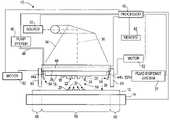
- a system 10 employed to form a relief pattern in a substrate 12includes a stage 14 upon which substrate 12 is supported, and a template 16 having a mold 18 with a patterning surface 20 thereon.
- substrate 12may be coupled to a substrate chuck (not shown), the substrate chuck (not shown) being any chuck including, but not limited to, vacuum and electromagnetic.
- Template 16 and/or mold 18may be formed from such materials including but not limited to, fused-silica, quartz, silicon, organic polymers, siloxane polymers, borosilicate glass, fluorocarbon polymers, metal, and hardened sapphire.
- patterning surface 20comprises features defined by a plurality of spaced-apart recessions 22 and protrusions 24 .
- patterning surface 20may be substantially smooth and/or planar. The plurality of features of patterning surface 20 defines an original pattern that forms the basis of a pattern to be formed on substrate 12 .
- Template 16may be coupled to an imprint head 26 to facilitate movement of template 16 , and therefore, mold 18 .
- template 16may be coupled to a template chuck (not shown), the template chuck (not shown) being any chuck including, but not limited to, vacuum and electromagnetic.
- a fluid dispense system 27is coupled to be selectively placed in fluid communication with substrate 12 so as to deposit a polymerizable material 28 thereon.
- polymerizable material 28may be deposited using any known technique, e.g., spin-coating, dip coating, chemical vapor deposition (CVD), physical vapor deposition (PVD), and the like. In the present example, however, polymerizable material 28 is deposited as a plurality of spaced-apart discrete droplets 30 on substrate 12 .
- a source 32 of energy 34is coupled to direct energy 34 along a path 36 .
- Imprint head 26 and stage 14are configured to arrange mold 18 and substrate 12 , respectively, to be in superimposition, and disposed in path 36 . Either imprint head 26 , stage 14 , or both vary a distance between mold 18 and substrate 12 to define a desired volume therebetween that is filled by polymerizable material 28 .
- polymerizable material 28is disposed upon substrate 12 before the desired volume is defined between mold 18 and substrate 12 .
- polymerizable material 28may fill the volume after the desired volume has been obtained.
- source 32produces energy 34 , which causes polymerizable material 28 to solidify and/or cross-link, forming a polymeric material conforming to the shape of a surface 38 of substrate 12 and patterning surface 20 of mold 18 .
- Control of this processis regulated by processor 40 that is in data communication with stage 14 , imprint head 26 , fluid dispense system 27 , and source 32 , operating on a computer-readable program stored in memory 42 .
- System 10further comprises a pair of conduits 44 a and 44 b .
- conduits 44 a and 44 bare coupled to imprint head 26 ; however, conduits 44 a and 44 b may be coupled to any part of system 10 , i.e., substrate 12 , stage 14 , template 16 , the substrate chuck (not shown), or the template chuck (not shown).
- system 10may comprise any number of conduits.
- Conduits 44 a and 44 bmay be in fluid communication with a pump system 46 via throughways 48 . As shown, throughways 48 are contained within imprint head 26 .
- throughways 48may be positioned anywhere throughout system 10 and may be coupled to any part of system 10 , i.e., substrate 12 , stage 14 , template 16 , the substrate chuck (not shown), or the template chuck (not shown).
- Pump system 46may be in communication with processor 40 operating on memory 42 to control an introduction/evacuation of a fluid 54 in an atmosphere 56 defined between mold 18 and droplets 30 , described further below.
- system 10comprises walls 50 coupled to imprint head 26 .
- walls 50may be coupled to any part of system 10 , i.e., substrate 12 , stage 14 , template 16 , the substrate chuck (not shown), or the template chuck (not shown).
- Walls 50may be positioned at an interface between first and second regions 58 and 60 of substrate 12 , with first region 58 being in superimposition with mold 18 and droplets 30 .
- walls 50may substantially surround imprint head 26 , and therefore, atmosphere 56 . However, for simplicity of illustration, walls 50 are shown surrounding a portion of imprint head 26 and atmosphere 56 .
- Walls 50may be in communication with a motor 52 , with motor 52 controlling a motion thereof.
- motor 52is shown as two separate bodies.
- Motor 52may comprise a solenoid selected from a group of solenoids including but not limited to, electric, pneumatic, and hydraulic. Further, motor 52 may be employed without feedback.
- Motor 52may be in communication with processor 40 operating on memory 42 .
- template 16 and therefore, mold 18are brought into proximity with substrate 12 before positioning polymerizable material 28 in droplets 30 upon substrate 12 .
- template 16is brought within hundreds of microns of substrate 12 , e.g., approximately 200 microns. It has been found desirable to perform localized control of atmosphere 56 that is proximate to both template 16 and substrate 12 .
- atmosphere 56For example, to avoid the deleterious effects of gases and/or gas pockets present in polymerizable material 28 in droplets 30 and/or subsequently trapped in a patterned layer, described further below, formed from droplets 30 , it has been found beneficial to control desired properties of atmosphere 56 and/or the pressure of atmosphere 56 . More specifically, it may be desired to control fluid 54 within atmosphere 56 . To that end, a system and a method to facilitate control of atmosphere 56 is described below.
- FIG. 2a portion of system 10 is shown. More specifically, mold 18 is shown spaced-apart from surface 38 of substrate 12 a first distance ‘d 1 ’. Distance ‘d 1 ’ may be on the order of hundreds of microns, i.e., approximately 200 to 300 microns. Walls 50 of system 10 are shown placed in a first position spaced-apart a distance ‘d 2 ’ from surface 38 of substrate 12 . Distance ‘d 2 ’ may be on the order of tens of microns, i.e., approximately 50 microns.
- Fluid 54may comprise a gas selected from a group of gases including, but not limited to, helium, hydrogen, nitrogen, carbon dioxide, and xenon. Fluid 54 may be introduced into atmosphere 56 through conduits 44 a and 44 b employing any desired method. For example, fluid 54 may be introduced through both conduits 44 a and 44 b concurrently, or sequentially pulsed through the same, i.e., first fluid is introduced through conduit 44 a and subsequently through conduit 44 b and then again through conduit 44 b , with the process being repeated for a desired time or during the entire imprinting process.
- conduits 44 a and 44 bmay introduce fluid 54 within atmosphere 56 at a flow rate of 9 liters/minute.
- atmosphere 56it may be desired to control atmosphere 56 , and more specifically, it may be desired to maintain fluid 54 within atmosphere 56 preceding to and until contact between mold 18 and polymerizable material 28 in droplets 30 . In a further embodiment, it may be desired to maintain fluid 54 within atmosphere 56 prior to and subsequent to contact between mold 18 and polymerizable material 28 in droplets 30 . In an example, it may be desired to have atmosphere 56 comprise more than a 95% mass fraction of fluid 54 therein. To that end, walls 50 facilitate control of atmosphere 56 by creating a flow resistance between first and second regions 58 and 60 of substrate 12 .
- walls 50are spaced-apart a distance ‘d 2 ’ from surface 38 of substrate 12 ; and mold 18 , in superimposition with polymerizable material 28 in droplets 30 , is spaced-apart a distance ‘d 1 ’ from surface 38 of substrate 12 . Further, distance ‘d 1 ’ is substantially greater than distance ‘d 2 ’. As a result, a greater resistance to a flow of fluid 54 is established between walls 50 and surface 38 of substrate 12 than between mold 18 and surface 38 of substrate 12 ; and thus, fluid 54 may tend to be maintained within atmosphere 56 , which may be desired.
- the distance ‘d 2 ’may be selected to achieve a desired resistance to the flow of fluid 54 between first and second regions 58 and 60 of substrate 12 .
- a desired volumeis defined between mold 18 and substrate 12 that is filled by polymerizable material 28 in droplets 30 .
- imprint head 26may position mold 18 such that polymerizable material 28 in droplets 30 are in contact therewith.
- walls 50may translate to minimize a probability of the same contacting substrate 12 during a decrease in a magnitude of distance ‘d 1 ’, and more specifically, during contact of mold 18 with polymerizable material 28 in droplets 30 .
- Contact of substrate 12 by walls 50may result in, inter alia, structural comprise of system 10 , impedance of contact between mold 18 and droplets 30 , misalignment of mold 18 with respect to substrate 12 , and damage to substrate 12 and/or mold 18 , all of which are undesirable.
- walls 50may translate in a first direction away from substrate 12 . More specifically, motor 52 may position walls 50 such that the same are positioned a distance ‘d 3 ’ from surface 38 of substrate 12 , with distance ‘d 3 ’ being greater than distance ‘d 1 ’. Distance ‘d 3 ’ may be on the order of hundreds of microns.
- mold 18is shown in mechanical contact with polymerizable material 28 , spreading droplets 30 , shown in FIG. 1 , so as to generate a contiguous formation 62 of polymerizable material 28 over surface 38 of substrate 12 .
- Template 16and further, mold 18 , may translate in a second direction towards substrate 12 , with the second direction being opposite to the aforementioned first direction.
- stage 14and further, substrate 12 may translate in a third direction towards mold 18 , with the third direction being in a direction substantially the same as the first direction.
- walls 50may translate in the first direction concurrently or asynchronously with translation of mold 18 and/or substrate 12 .
- fluid 54may be introduced into atmosphere 56 at any time prior to contact between mold 18 and droplets 30 .
- introduction of fluid 54 into atmosphere 56may be ceased at any time.
- walls 50 a and 50 bmay be positioned distance ‘d 2 ’ from surface 38 of substrate 12 , as mentioned above.
- wall 50 cmay be positioned a distance ‘d 4 ’ from surface 38 of substrate 12 .
- Distance ‘d 4 ’may have a magnitude approximately between 200 microns and 1 millimeter.
- atmosphere 56may be exposed to an ambient environment.
- walls 50may substantially surround imprint head 26 , and thus atmosphere 56 , forming a chamber (not shown).
- the chamber (not shown)may be completely evacuated or pressurized.
- distance ‘d 1 ’may be increased prior to contact of mold 18 with droplets 30 . More specifically, distance ‘d 1 ’ may be on the order of millimeters, i.e., approximately 1 millimeter.
Landscapes
- Engineering & Computer Science (AREA)
- Nanotechnology (AREA)
- Chemical & Material Sciences (AREA)
- Physics & Mathematics (AREA)
- Mechanical Engineering (AREA)
- General Physics & Mathematics (AREA)
- Crystallography & Structural Chemistry (AREA)
- Condensed Matter Physics & Semiconductors (AREA)
- Manufacturing & Machinery (AREA)
- Mathematical Physics (AREA)
- Theoretical Computer Science (AREA)
- Shaping Of Tube Ends By Bending Or Straightening (AREA)
- Exposure Of Semiconductors, Excluding Electron Or Ion Beam Exposure (AREA)
Abstract
Description
Claims (20)
Priority Applications (3)
| Application Number | Priority Date | Filing Date | Title |
|---|---|---|---|
| US11/231,580US7670534B2 (en) | 2005-09-21 | 2005-09-21 | Method to control an atmosphere between a body and a substrate |
| US11/231,616US7316554B2 (en) | 2005-09-21 | 2005-09-21 | System to control an atmosphere between a body and a substrate |
| US12/688,190US7931846B2 (en) | 2005-09-21 | 2010-01-15 | Method to control an atmosphere between a body and a substrate |
Applications Claiming Priority (1)
| Application Number | Priority Date | Filing Date | Title |
|---|---|---|---|
| US11/231,580US7670534B2 (en) | 2005-09-21 | 2005-09-21 | Method to control an atmosphere between a body and a substrate |
Related Child Applications (2)
| Application Number | Title | Priority Date | Filing Date |
|---|---|---|---|
| US11/231,616ContinuationUS7316554B2 (en) | 2005-09-21 | 2005-09-21 | System to control an atmosphere between a body and a substrate |
| US12/688,190ContinuationUS7931846B2 (en) | 2005-09-21 | 2010-01-15 | Method to control an atmosphere between a body and a substrate |
Publications (2)
| Publication Number | Publication Date |
|---|---|
| US20070063384A1 US20070063384A1 (en) | 2007-03-22 |
| US7670534B2true US7670534B2 (en) | 2010-03-02 |
Family
ID=37883265
Family Applications (3)
| Application Number | Title | Priority Date | Filing Date |
|---|---|---|---|
| US11/231,616Active2025-12-24US7316554B2 (en) | 2005-09-21 | 2005-09-21 | System to control an atmosphere between a body and a substrate |
| US11/231,580Active2028-09-20US7670534B2 (en) | 2005-09-21 | 2005-09-21 | Method to control an atmosphere between a body and a substrate |
| US12/688,190Expired - LifetimeUS7931846B2 (en) | 2005-09-21 | 2010-01-15 | Method to control an atmosphere between a body and a substrate |
Family Applications Before (1)
| Application Number | Title | Priority Date | Filing Date |
|---|---|---|---|
| US11/231,616Active2025-12-24US7316554B2 (en) | 2005-09-21 | 2005-09-21 | System to control an atmosphere between a body and a substrate |
Family Applications After (1)
| Application Number | Title | Priority Date | Filing Date |
|---|---|---|---|
| US12/688,190Expired - LifetimeUS7931846B2 (en) | 2005-09-21 | 2010-01-15 | Method to control an atmosphere between a body and a substrate |
Country Status (1)
| Country | Link |
|---|---|
| US (3) | US7316554B2 (en) |
Cited By (14)
| Publication number | Priority date | Publication date | Assignee | Title |
|---|---|---|---|---|
| US20060125154A1 (en)* | 2004-01-15 | 2006-06-15 | Molecular Imprints, Inc. | Method to improve the flow rate of imprinting material employing an absorption layer |
| US20090148619A1 (en)* | 2007-12-05 | 2009-06-11 | Molecular Imprints, Inc. | Controlling Thickness of Residual Layer |
| US20090273119A1 (en)* | 2006-03-10 | 2009-11-05 | Tetsuya Imai | Imprint Method and Imprint Apparatus |
| US20100096764A1 (en)* | 2008-10-20 | 2010-04-22 | Molecular Imprints, Inc. | Gas Environment for Imprint Lithography |
| US20100112220A1 (en)* | 2008-11-03 | 2010-05-06 | Molecular Imprints, Inc. | Dispense system set-up and characterization |
| US20100119637A1 (en)* | 2005-09-21 | 2010-05-13 | Molecular Imprints, Inc. | Method to Control an Atmosphere Between a Body and a Substrate |
| US20100237042A1 (en)* | 2009-03-23 | 2010-09-23 | Intevac, Inc. | Process for optimization of island to trench ratio in patterned media |
| US20120080820A1 (en)* | 2010-10-04 | 2012-04-05 | Canon Kabushiki Kaisha | Imprinting method |
| US20120080825A1 (en)* | 2010-09-30 | 2012-04-05 | Soichiro Mitsui | Imprinting lithography apparatus and imprinting lithography method |
| US20140191441A1 (en)* | 2011-09-21 | 2014-07-10 | Canon Kabushiki Kaisha | Imprint apparatus and article manufacturing method using same |
| US9811671B1 (en) | 2000-05-24 | 2017-11-07 | Copilot Ventures Fund Iii Llc | Authentication method and system |
| US9846814B1 (en) | 2008-04-23 | 2017-12-19 | Copilot Ventures Fund Iii Llc | Authentication method and system |
| US11198235B2 (en) | 2018-08-09 | 2021-12-14 | Canon Kabushiki Kaisha | Flexible mask modulation for controlling atmosphere between mask and substrate and methods of using the same |
| US11590687B2 (en) | 2020-06-30 | 2023-02-28 | Canon Kabushiki Kaisha | Systems and methods for reducing pressure while shaping a film |
Families Citing this family (47)
| Publication number | Priority date | Publication date | Assignee | Title |
|---|---|---|---|---|
| US20080160129A1 (en)* | 2006-05-11 | 2008-07-03 | Molecular Imprints, Inc. | Template Having a Varying Thickness to Facilitate Expelling a Gas Positioned Between a Substrate and the Template |
| US7077992B2 (en)* | 2002-07-11 | 2006-07-18 | Molecular Imprints, Inc. | Step and repeat imprint lithography processes |
| US7019819B2 (en) | 2002-11-13 | 2006-03-28 | Molecular Imprints, Inc. | Chucking system for modulating shapes of substrates |
| US7442336B2 (en)* | 2003-08-21 | 2008-10-28 | Molecular Imprints, Inc. | Capillary imprinting technique |
| US7641840B2 (en) | 2002-11-13 | 2010-01-05 | Molecular Imprints, Inc. | Method for expelling gas positioned between a substrate and a mold |
| US8211214B2 (en)* | 2003-10-02 | 2012-07-03 | Molecular Imprints, Inc. | Single phase fluid imprint lithography method |
| US20060062922A1 (en) | 2004-09-23 | 2006-03-23 | Molecular Imprints, Inc. | Polymerization technique to attenuate oxygen inhibition of solidification of liquids and composition therefor |
| US7906058B2 (en)* | 2005-12-01 | 2011-03-15 | Molecular Imprints, Inc. | Bifurcated contact printing technique |
| MY144847A (en)* | 2005-12-08 | 2011-11-30 | Molecular Imprints Inc | Method and system for double-sided patterning of substrates |
| US7670530B2 (en)* | 2006-01-20 | 2010-03-02 | Molecular Imprints, Inc. | Patterning substrates employing multiple chucks |
| KR20080114681A (en)* | 2006-04-03 | 2008-12-31 | 몰레큘러 임프린츠 인코퍼레이티드 | Lithography Imprinting System |
| US8215946B2 (en) | 2006-05-18 | 2012-07-10 | Molecular Imprints, Inc. | Imprint lithography system and method |
| DE102006024524A1 (en)* | 2006-05-23 | 2007-12-06 | Von Ardenne Anlagentechnik Gmbh | Transparent multi-layer composite system capable of reflecting infrared radiation for hardening and/or shaping of substrates and temperature process, comprises layers, anti-reflection coating, blocking layer and dielectric interface layer |
| TW200842934A (en)* | 2006-12-29 | 2008-11-01 | Molecular Imprints Inc | Imprint fluid control |
| US20090014917A1 (en)* | 2007-07-10 | 2009-01-15 | Molecular Imprints, Inc. | Drop Pattern Generation for Imprint Lithography |
| JP2009034926A (en)* | 2007-08-02 | 2009-02-19 | Sumitomo Electric Ind Ltd | Resin pattern forming method |
| US8144309B2 (en)* | 2007-09-05 | 2012-03-27 | Asml Netherlands B.V. | Imprint lithography |
| US8119052B2 (en)* | 2007-11-02 | 2012-02-21 | Molecular Imprints, Inc. | Drop pattern generation for imprint lithography |
| US8361371B2 (en)* | 2008-02-08 | 2013-01-29 | Molecular Imprints, Inc. | Extrusion reduction in imprint lithography |
| JP5235506B2 (en)* | 2008-06-02 | 2013-07-10 | キヤノン株式会社 | Pattern transfer apparatus and device manufacturing method |
| WO2010004006A2 (en)* | 2008-07-10 | 2010-01-14 | Singulus Technologies Ag | Device and method for impressing structures in a substrate, in particular in optical data storage media, semiconductor structures and microstructures |
| US8512797B2 (en)* | 2008-10-21 | 2013-08-20 | Molecular Imprints, Inc. | Drop pattern generation with edge weighting |
| US8586126B2 (en) | 2008-10-21 | 2013-11-19 | Molecular Imprints, Inc. | Robust optimization to generate drop patterns in imprint lithography which are tolerant of variations in drop volume and drop placement |
| JP5175771B2 (en)* | 2009-02-27 | 2013-04-03 | 株式会社日立ハイテクノロジーズ | Fine structure transfer apparatus and fine structure transfer method |
| EP2287666B1 (en)* | 2009-08-22 | 2012-06-27 | EV Group E. Thallner GmbH | Device for embossing substrates |
| JP2011071500A (en)* | 2009-08-31 | 2011-04-07 | Fujifilm Corp | Pattern transfer apparatus and pattern forming method |
| WO2011064021A1 (en)* | 2009-11-30 | 2011-06-03 | Asml Netherlands B.V. | Imprint lithography apparatus and method |
| US8691134B2 (en)* | 2010-01-28 | 2014-04-08 | Molecular Imprints, Inc. | Roll-to-roll imprint lithography and purging system |
| JP5848263B2 (en)* | 2010-02-09 | 2016-01-27 | モレキュラー・インプリンツ・インコーポレーテッド | Process gas confinement for nanoimprint |
| JP5491931B2 (en)* | 2010-03-30 | 2014-05-14 | 富士フイルム株式会社 | Nanoimprint method and mold manufacturing method |
| JP6230041B2 (en)* | 2013-04-18 | 2017-11-15 | キヤノン株式会社 | Imprint apparatus and article manufacturing method using the same |
| KR102056902B1 (en) | 2013-05-29 | 2019-12-18 | 삼성전자주식회사 | Wire grid polarizer and liquid crystal display panel and liquid crystal display device having the same |
| KR102089661B1 (en) | 2013-08-27 | 2020-03-17 | 삼성전자주식회사 | Wire grid polarizer and liquid crystal display panel and liquid crystal display device having the same |
| JP2015056548A (en)* | 2013-09-12 | 2015-03-23 | 大日本印刷株式会社 | Imprint apparatus and imprint method |
| JP6294679B2 (en)* | 2014-01-21 | 2018-03-14 | キヤノン株式会社 | Imprint apparatus and article manufacturing method |
| JP6445772B2 (en)* | 2014-03-17 | 2018-12-26 | キヤノン株式会社 | Imprint apparatus and article manufacturing method |
| EP2960059B1 (en) | 2014-06-25 | 2018-10-24 | Universal Display Corporation | Systems and methods of modulating flow during vapor jet deposition of organic materials |
| US11220737B2 (en) | 2014-06-25 | 2022-01-11 | Universal Display Corporation | Systems and methods of modulating flow during vapor jet deposition of organic materials |
| US11267012B2 (en)* | 2014-06-25 | 2022-03-08 | Universal Display Corporation | Spatial control of vapor condensation using convection |
| JP6525567B2 (en)* | 2014-12-02 | 2019-06-05 | キヤノン株式会社 | Imprint apparatus and method of manufacturing article |
| US10566534B2 (en) | 2015-10-12 | 2020-02-18 | Universal Display Corporation | Apparatus and method to deliver organic material via organic vapor-jet printing (OVJP) |
| JP6643048B2 (en)* | 2015-11-09 | 2020-02-12 | キヤノン株式会社 | Apparatus for processing substrate, method for manufacturing article, and gas supply path |
| JP6700771B2 (en)* | 2015-12-16 | 2020-05-27 | キヤノン株式会社 | Imprint apparatus and article manufacturing method |
| JP6808386B2 (en)* | 2016-07-12 | 2021-01-06 | キヤノン株式会社 | Imprint equipment and article manufacturing method |
| US10895806B2 (en)* | 2017-09-29 | 2021-01-19 | Canon Kabushiki Kaisha | Imprinting method and apparatus |
| JP2021027107A (en) | 2019-08-01 | 2021-02-22 | キヤノン株式会社 | Imprint apparatus, imprint method, and article manufacturing method |
| US20240231220A9 (en)* | 2022-10-24 | 2024-07-11 | Canon Kabushiki Kaisha | Planarization process, apparatus and method of manufacturing an article |
Citations (104)
| Publication number | Priority date | Publication date | Assignee | Title |
|---|---|---|---|---|
| US4279628A (en) | 1979-12-31 | 1981-07-21 | Energy Synergistics, Inc. | Apparatus for drying a natural gas stream |
| US4512848A (en) | 1984-02-06 | 1985-04-23 | Exxon Research And Engineering Co. | Procedure for fabrication of microstructures over large areas using physical replication |
| US4521175A (en) | 1980-03-14 | 1985-06-04 | Multivac Sepp Haggenmuller Kg | Apparatus for producing containers from thermoplastic sheet material |
| US4689004A (en) | 1985-04-18 | 1987-08-25 | Firma Carl Freudenberg | Apparatus for adhering thermally-softenable plastic particles into a plastic body |
| US4731155A (en) | 1987-04-15 | 1988-03-15 | General Electric Company | Process for forming a lithographic mask |
| US4767584A (en) | 1985-04-03 | 1988-08-30 | Massachusetts Institute Of Technology | Process of and apparatus for producing design patterns in materials |
| US4848911A (en) | 1986-06-11 | 1989-07-18 | Kabushiki Kaisha Toshiba | Method for aligning first and second objects, relative to each other, and apparatus for practicing this method |
| US4959252A (en) | 1986-09-29 | 1990-09-25 | Rhone-Poulenc Chimie | Highly oriented thermotropic optical disc member |
| US5028366A (en) | 1988-01-12 | 1991-07-02 | Air Products And Chemicals, Inc. | Water based mold release compositions for making molded polyurethane foam |
| US5110514A (en) | 1989-05-01 | 1992-05-05 | Soane Technologies, Inc. | Controlled casting of a shrinkable material |
| US5148037A (en) | 1988-09-09 | 1992-09-15 | Canon Kabushiki Kaisha | Position detecting method and apparatus |
| US5151754A (en) | 1989-10-06 | 1992-09-29 | Kabushiki Kaisha Toshiba | Method and an apparatus for measuring a displacement between two objects and a method and an apparatus for measuring a gap distance between two objects |
| US5240550A (en) | 1990-09-21 | 1993-08-31 | U.S. Philips Corp. | Method of forming at least one groove in a substrate layer |
| US5259926A (en) | 1991-09-24 | 1993-11-09 | Hitachi, Ltd. | Method of manufacturing a thin-film pattern on a substrate |
| US5338177A (en) | 1992-04-22 | 1994-08-16 | Societe Nationale Industrielle Et Aerospatiale | Hot compacting device for the production of parts requiring simultaneous pressure and temperature rises |
| US5362940A (en) | 1990-11-09 | 1994-11-08 | Litel Instruments | Use of Fresnel zone plates for material processing |
| US5371822A (en) | 1992-06-09 | 1994-12-06 | Digital Equipment Corporation | Method of packaging and assembling opto-electronic integrated circuits |
| US5425848A (en) | 1993-03-16 | 1995-06-20 | U.S. Philips Corporation | Method of providing a patterned relief of cured photoresist on a flat substrate surface and device for carrying out such a method |
| US5480047A (en) | 1993-06-04 | 1996-01-02 | Sharp Kabushiki Kaisha | Method for forming a fine resist pattern |
| US5512131A (en) | 1993-10-04 | 1996-04-30 | President And Fellows Of Harvard College | Formation of microstamped patterns on surfaces and derivative articles |
| US5545367A (en) | 1992-04-15 | 1996-08-13 | Soane Technologies, Inc. | Rapid prototype three dimensional stereolithography |
| US5601641A (en) | 1992-07-21 | 1997-02-11 | Tse Industries, Inc. | Mold release composition with polybutadiene and method of coating a mold core |
| US5669303A (en) | 1996-03-04 | 1997-09-23 | Motorola | Apparatus and method for stamping a surface |
| US5694961A (en) | 1993-02-25 | 1997-12-09 | J.M. Voith Gmbh | Device and method for changing the flow resistance of a fluid flow control device |
| US5772905A (en) | 1995-11-15 | 1998-06-30 | Regents Of The University Of Minnesota | Nanoimprint lithography |
| US5776748A (en) | 1993-10-04 | 1998-07-07 | President And Fellows Of Harvard College | Method of formation of microstamped patterns on plates for adhesion of cells and other biological materials, devices and uses therefor |
| US5812629A (en) | 1997-04-30 | 1998-09-22 | Clauser; John F. | Ultrahigh resolution interferometric x-ray imaging |
| US5820769A (en) | 1995-05-24 | 1998-10-13 | Regents Of The University Of Minnesota | Method for making magnetic storage having discrete elements with quantized magnetic moments |
| US5821175A (en) | 1988-07-08 | 1998-10-13 | Cauldron Limited Partnership | Removal of surface contaminants by irradiation using various methods to achieve desired inert gas flow over treated surface |
| US5849209A (en) | 1995-03-31 | 1998-12-15 | Johnson & Johnson Vision Products, Inc. | Mold material made with additives |
| US5849222A (en) | 1995-09-29 | 1998-12-15 | Johnson & Johnson Vision Products, Inc. | Method for reducing lens hole defects in production of contact lens blanks |
| US5858580A (en) | 1997-09-17 | 1999-01-12 | Numerical Technologies, Inc. | Phase shifting circuit manufacture method and apparatus |
| US5888650A (en) | 1996-06-03 | 1999-03-30 | Minnesota Mining And Manufacturing Company | Temperature-responsive adhesive article |
| US5948470A (en) | 1997-04-28 | 1999-09-07 | Harrison; Christopher | Method of nanoscale patterning and products made thereby |
| US5974150A (en) | 1997-09-30 | 1999-10-26 | Tracer Detection Technology Corp. | System and method for authentication of goods |
| US5997963A (en) | 1998-05-05 | 1999-12-07 | Ultratech Stepper, Inc. | Microchamber |
| US6046056A (en) | 1996-06-28 | 2000-04-04 | Caliper Technologies Corporation | High throughput screening assay systems in microscale fluidic devices |
| US6074827A (en) | 1996-07-30 | 2000-06-13 | Aclara Biosciences, Inc. | Microfluidic method for nucleic acid purification and processing |
| US6099771A (en) | 1998-07-08 | 2000-08-08 | Lear Corporation | Vacuum compression method for forming molded thermoplastic floor mat having a "Class A" finish |
| US6159400A (en) | 1995-08-01 | 2000-12-12 | Laquer; Henry Louis | Method for deforming solids in a controlled atmosphere and at adjustable rates, pressures and temperature |
| US6218316B1 (en) | 1998-10-22 | 2001-04-17 | Micron Technology, Inc. | Planarization of non-planar surfaces in device fabrication |
| US6257866B1 (en) | 1996-06-18 | 2001-07-10 | Hy-Tech Forming Systems, Inc. | Apparatus for accurately forming plastic sheet |
| US6274294B1 (en) | 1999-02-03 | 2001-08-14 | Electroformed Stents, Inc. | Cylindrical photolithography exposure process and apparatus |
| US6309580B1 (en) | 1995-11-15 | 2001-10-30 | Regents Of The University Of Minnesota | Release surfaces, particularly for use in nanoimprint lithography |
| US6326627B1 (en) | 2000-08-02 | 2001-12-04 | Archimedes Technology Group, Inc. | Mass filtering sputtered ion source |
| US6334960B1 (en) | 1999-03-11 | 2002-01-01 | Board Of Regents, The University Of Texas System | Step and flash imprint lithography |
| US20020018190A1 (en) | 2000-06-15 | 2002-02-14 | Hideki Nogawa | Exposure apparatus and device manufacturing method |
| US6348999B1 (en) | 1995-05-10 | 2002-02-19 | Epigem Limited | Micro relief element and preparation thereof |
| US6355198B1 (en) | 1996-03-15 | 2002-03-12 | President And Fellows Of Harvard College | Method of forming articles including waveguides via capillary micromolding and microtransfer molding |
| US20020042027A1 (en) | 1998-10-09 | 2002-04-11 | Chou Stephen Y. | Microscale patterning and articles formed thereby |
| US6391217B2 (en) | 1999-12-23 | 2002-05-21 | University Of Massachusetts | Methods and apparatus for forming submicron patterns on films |
| US6416311B1 (en) | 1998-05-04 | 2002-07-09 | Jenoptik Aktiengesellschaft | Device and method for separating a shaped substrate from a stamping tool |
| US20020132482A1 (en) | 2000-07-18 | 2002-09-19 | Chou Stephen Y. | Fluid pressure imprint lithography |
| US6461524B1 (en) | 1999-05-27 | 2002-10-08 | Sanyo Electric Co., Ltd. | Method of filtering a fluid |
| US20020168578A1 (en) | 1996-09-18 | 2002-11-14 | Numerical Technologies, Inc. | Phase shifting circuit manufacture method and apparatus |
| US20020170880A1 (en) | 2001-03-22 | 2002-11-21 | Yong Chen | Scanning probe based lithographic alignment |
| US6498640B1 (en) | 1999-12-30 | 2002-12-24 | Koninklijke Philips Electronics N.V. | Method to measure alignment using latent image grating structures |
| US20030025895A1 (en) | 2001-08-03 | 2003-02-06 | Michael Binnard | Apparatus and methods for detecting tool-induced shift in microlithography apparatus |
| US6518189B1 (en) | 1995-11-15 | 2003-02-11 | Regents Of The University Of Minnesota | Method and apparatus for high density nanostructures |
| US6517995B1 (en) | 1999-09-14 | 2003-02-11 | Massachusetts Institute Of Technology | Fabrication of finely featured devices by liquid embossing |
| US6517977B2 (en) | 2001-03-28 | 2003-02-11 | Motorola, Inc. | Lithographic template and method of formation and use |
| US20030062334A1 (en) | 2001-09-25 | 2003-04-03 | Lee Hong Hie | Method for forming a micro-pattern on a substrate by using capillary force |
| US20030081193A1 (en) | 2001-06-01 | 2003-05-01 | White Donald L. | Holder, system, and process for improving overlay in lithography |
| US20030080472A1 (en) | 2001-10-29 | 2003-05-01 | Chou Stephen Y. | Lithographic method with bonded release layer for molding small patterns |
| US6580172B2 (en) | 2001-03-02 | 2003-06-17 | Motorola, Inc. | Lithographic template and method of formation and use |
| US20030137494A1 (en) | 2000-05-01 | 2003-07-24 | Tulbert David J. | Human-machine interface |
| US6621960B2 (en) | 2002-01-24 | 2003-09-16 | Oplink Communications, Inc. | Method of fabricating multiple superimposed fiber Bragg gratings |
| US20030174435A1 (en) | 2002-03-18 | 2003-09-18 | International Business Machines Corporation | Method and apparatus for providing an aligned coil for an inductive head structure using a patterned seed layer |
| US20030186140A1 (en) | 2001-06-27 | 2003-10-02 | Fries David P. | Maskless photolithography for using photoreactive agents |
| US6646662B1 (en) | 1998-05-26 | 2003-11-11 | Seiko Epson Corporation | Patterning method, patterning apparatus, patterning template, and method for manufacturing the patterning template |
| US6696220B2 (en) | 2000-10-12 | 2004-02-24 | Board Of Regents, The University Of Texas System | Template for room temperature, low pressure micro-and nano-imprint lithography |
| US20040036201A1 (en) | 2000-07-18 | 2004-02-26 | Princeton University | Methods and apparatus of field-induced pressure imprint lithography |
| US20040046288A1 (en) | 2000-07-18 | 2004-03-11 | Chou Stephen Y. | Laset assisted direct imprint lithography |
| US20040046271A1 (en)* | 2002-09-05 | 2004-03-11 | Watts Michael P.C. | Functional patterning material for imprint lithography processes |
| US20040110856A1 (en) | 2002-12-04 | 2004-06-10 | Young Jung Gun | Polymer solution for nanoimprint lithography to reduce imprint temperature and pressure |
| US20040131718A1 (en) | 2000-07-18 | 2004-07-08 | Princeton University | Lithographic apparatus for fluid pressure imprint lithography |
| US20040129293A1 (en) | 2003-01-08 | 2004-07-08 | Eichenberger Louis C. | Flow system flush process |
| US20040132301A1 (en)* | 2002-09-12 | 2004-07-08 | Harper Bruce M. | Indirect fluid pressure imprinting |
| US20040137734A1 (en) | 1995-11-15 | 2004-07-15 | Princeton University | Compositions and processes for nanoimprinting |
| US6764386B2 (en) | 2002-01-11 | 2004-07-20 | Applied Materials, Inc. | Air bearing-sealed micro-processing chamber |
| US20040156108A1 (en) | 2001-10-29 | 2004-08-12 | Chou Stephen Y. | Articles comprising nanoscale patterns with reduced edge roughness and methods of making same |
| US6776094B1 (en) | 1993-10-04 | 2004-08-17 | President & Fellows Of Harvard College | Kit For Microcontact Printing |
| US20040192041A1 (en) | 2003-03-27 | 2004-09-30 | Jun-Ho Jeong | UV nanoimprint lithography process using elementwise embossed stamp and selectively additive pressurization |
| US20040197843A1 (en) | 2001-07-25 | 2004-10-07 | Chou Stephen Y. | Nanochannel arrays and their preparation and use for high throughput macromolecular analysis |
| US20040200368A1 (en)* | 2003-03-20 | 2004-10-14 | Masahiko Ogino | Mold structures, and method of transfer of fine structures |
| US20040219249A1 (en)* | 2003-05-02 | 2004-11-04 | Yong-Chen Chung | Uniform pressing apparatus |
| US20040250945A1 (en) | 2003-06-10 | 2004-12-16 | Industrial Technology Research Institute | Method for and apparatus for bonding patterned imprint to a substrate by adhering means |
| US6849558B2 (en) | 2002-05-22 | 2005-02-01 | The Board Of Trustees Of The Leland Stanford Junior University | Replication and transfer of microstructures and nanostructures |
| US20050037143A1 (en) | 2000-07-18 | 2005-02-17 | Chou Stephen Y. | Imprint lithography with improved monitoring and control and apparatus therefor |
| US6869890B2 (en) | 2001-01-09 | 2005-03-22 | Ebara Corporation | Processing apparatus to be sealed against workpiece |
| US20050064054A1 (en)* | 2003-09-24 | 2005-03-24 | Canon Kabushiki Kaisha | Pattern forming apparatus |
| US6873087B1 (en) | 1999-10-29 | 2005-03-29 | Board Of Regents, The University Of Texas System | High precision orientation alignment and gap control stages for imprint lithography processes |
| US20050072755A1 (en)* | 2003-10-02 | 2005-04-07 | University Of Texas System Board Of Regents | Single phase fluid imprint lithography method |
| US6900881B2 (en) | 2002-07-11 | 2005-05-31 | Molecular Imprints, Inc. | Step and repeat imprint lithography systems |
| US6908861B2 (en) | 2002-07-11 | 2005-06-21 | Molecular Imprints, Inc. | Method for imprint lithography using an electric field |
| US6916584B2 (en) | 2002-08-01 | 2005-07-12 | Molecular Imprints, Inc. | Alignment methods for imprint lithography |
| US6916585B2 (en) | 2000-07-16 | 2005-07-12 | Board Of Regents, The University Of Texas Systems | Method of varying template dimensions to achieve alignment during imprint lithography |
| US6932934B2 (en) | 2002-07-11 | 2005-08-23 | Molecular Imprints, Inc. | Formation of discontinuous films during an imprint lithography process |
| US6964793B2 (en) | 2002-05-16 | 2005-11-15 | Board Of Regents, The University Of Texas System | Method for fabricating nanoscale patterns in light curable compositions using an electric field |
| US6982783B2 (en) | 2002-11-13 | 2006-01-03 | Molecular Imprints, Inc. | Chucking system for modulating shapes of substrates |
| US20060076717A1 (en) | 2002-07-11 | 2006-04-13 | Molecular Imprints, Inc. | Step and repeat imprint lithography processes |
| US7128875B2 (en) | 1995-04-10 | 2006-10-31 | Cubicciotti Roger S | Signal processing devices comprising biological and bio-mimetic components |
| US20070065532A1 (en) | 2005-09-21 | 2007-03-22 | Molecular Imprints, Inc. | System to control an atmosphere between a body and a substrate |
| US20070243279A1 (en)* | 2005-01-31 | 2007-10-18 | Molecular Imprints, Inc. | Imprint Lithography Template to Facilitate Control of Liquid Movement |
Family Cites Families (5)
| Publication number | Priority date | Publication date | Assignee | Title |
|---|---|---|---|---|
| DE10010001A1 (en)* | 2000-03-02 | 2001-09-06 | Celanese Ventures Gmbh | Membranes useful in fuel cells comprise a blend of sulfonated aryl polymer, aminated or nitrated polyether(ether)sulfone and plasticizer |
| JP4233802B2 (en)* | 2002-04-26 | 2009-03-04 | 東レエンジニアリング株式会社 | Mounting method and mounting apparatus |
| WO2005018702A2 (en)* | 2003-08-13 | 2005-03-03 | Medtronic, Inc. | Active agent delivery systems including a miscible polymer blend, medical devices, and methods |
| US7329114B2 (en)* | 2004-01-20 | 2008-02-12 | Komag, Inc. | Isothermal imprint embossing system |
| US20050155554A1 (en)* | 2004-01-20 | 2005-07-21 | Saito Toshiyuki M. | Imprint embossing system |
- 2005
- 2005-09-21USUS11/231,616patent/US7316554B2/enactiveActive
- 2005-09-21USUS11/231,580patent/US7670534B2/enactiveActive
- 2010
- 2010-01-15USUS12/688,190patent/US7931846B2/ennot_activeExpired - Lifetime
Patent Citations (126)
| Publication number | Priority date | Publication date | Assignee | Title |
|---|---|---|---|---|
| US4279628A (en) | 1979-12-31 | 1981-07-21 | Energy Synergistics, Inc. | Apparatus for drying a natural gas stream |
| US4521175A (en) | 1980-03-14 | 1985-06-04 | Multivac Sepp Haggenmuller Kg | Apparatus for producing containers from thermoplastic sheet material |
| US4512848A (en) | 1984-02-06 | 1985-04-23 | Exxon Research And Engineering Co. | Procedure for fabrication of microstructures over large areas using physical replication |
| US4767584A (en) | 1985-04-03 | 1988-08-30 | Massachusetts Institute Of Technology | Process of and apparatus for producing design patterns in materials |
| US4689004A (en) | 1985-04-18 | 1987-08-25 | Firma Carl Freudenberg | Apparatus for adhering thermally-softenable plastic particles into a plastic body |
| US4848911A (en) | 1986-06-11 | 1989-07-18 | Kabushiki Kaisha Toshiba | Method for aligning first and second objects, relative to each other, and apparatus for practicing this method |
| US4959252A (en) | 1986-09-29 | 1990-09-25 | Rhone-Poulenc Chimie | Highly oriented thermotropic optical disc member |
| US4731155A (en) | 1987-04-15 | 1988-03-15 | General Electric Company | Process for forming a lithographic mask |
| US5028366A (en) | 1988-01-12 | 1991-07-02 | Air Products And Chemicals, Inc. | Water based mold release compositions for making molded polyurethane foam |
| US5821175A (en) | 1988-07-08 | 1998-10-13 | Cauldron Limited Partnership | Removal of surface contaminants by irradiation using various methods to achieve desired inert gas flow over treated surface |
| US5148037A (en) | 1988-09-09 | 1992-09-15 | Canon Kabushiki Kaisha | Position detecting method and apparatus |
| US5110514A (en) | 1989-05-01 | 1992-05-05 | Soane Technologies, Inc. | Controlled casting of a shrinkable material |
| US5151754A (en) | 1989-10-06 | 1992-09-29 | Kabushiki Kaisha Toshiba | Method and an apparatus for measuring a displacement between two objects and a method and an apparatus for measuring a gap distance between two objects |
| US5240550A (en) | 1990-09-21 | 1993-08-31 | U.S. Philips Corp. | Method of forming at least one groove in a substrate layer |
| US5362940A (en) | 1990-11-09 | 1994-11-08 | Litel Instruments | Use of Fresnel zone plates for material processing |
| US5259926A (en) | 1991-09-24 | 1993-11-09 | Hitachi, Ltd. | Method of manufacturing a thin-film pattern on a substrate |
| US5545367A (en) | 1992-04-15 | 1996-08-13 | Soane Technologies, Inc. | Rapid prototype three dimensional stereolithography |
| US5338177A (en) | 1992-04-22 | 1994-08-16 | Societe Nationale Industrielle Et Aerospatiale | Hot compacting device for the production of parts requiring simultaneous pressure and temperature rises |
| US5371822A (en) | 1992-06-09 | 1994-12-06 | Digital Equipment Corporation | Method of packaging and assembling opto-electronic integrated circuits |
| US5601641A (en) | 1992-07-21 | 1997-02-11 | Tse Industries, Inc. | Mold release composition with polybutadiene and method of coating a mold core |
| US5694961A (en) | 1993-02-25 | 1997-12-09 | J.M. Voith Gmbh | Device and method for changing the flow resistance of a fluid flow control device |
| US5425848A (en) | 1993-03-16 | 1995-06-20 | U.S. Philips Corporation | Method of providing a patterned relief of cured photoresist on a flat substrate surface and device for carrying out such a method |
| US5480047A (en) | 1993-06-04 | 1996-01-02 | Sharp Kabushiki Kaisha | Method for forming a fine resist pattern |
| US5776748A (en) | 1993-10-04 | 1998-07-07 | President And Fellows Of Harvard College | Method of formation of microstamped patterns on plates for adhesion of cells and other biological materials, devices and uses therefor |
| US6776094B1 (en) | 1993-10-04 | 2004-08-17 | President & Fellows Of Harvard College | Kit For Microcontact Printing |
| US5512131A (en) | 1993-10-04 | 1996-04-30 | President And Fellows Of Harvard College | Formation of microstamped patterns on surfaces and derivative articles |
| US5849209A (en) | 1995-03-31 | 1998-12-15 | Johnson & Johnson Vision Products, Inc. | Mold material made with additives |
| US7128875B2 (en) | 1995-04-10 | 2006-10-31 | Cubicciotti Roger S | Signal processing devices comprising biological and bio-mimetic components |
| US6348999B1 (en) | 1995-05-10 | 2002-02-19 | Epigem Limited | Micro relief element and preparation thereof |
| US5820769A (en) | 1995-05-24 | 1998-10-13 | Regents Of The University Of Minnesota | Method for making magnetic storage having discrete elements with quantized magnetic moments |
| US5956216A (en) | 1995-05-24 | 1999-09-21 | Regents Of The University Of Minnesota | Magnetic storage having discrete elements with quantized magnetic moments |
| US6159400A (en) | 1995-08-01 | 2000-12-12 | Laquer; Henry Louis | Method for deforming solids in a controlled atmosphere and at adjustable rates, pressures and temperature |
| US5849222A (en) | 1995-09-29 | 1998-12-15 | Johnson & Johnson Vision Products, Inc. | Method for reducing lens hole defects in production of contact lens blanks |
| US20040137734A1 (en) | 1995-11-15 | 2004-07-15 | Princeton University | Compositions and processes for nanoimprinting |
| US6309580B1 (en) | 1995-11-15 | 2001-10-30 | Regents Of The University Of Minnesota | Release surfaces, particularly for use in nanoimprint lithography |
| US6518189B1 (en) | 1995-11-15 | 2003-02-11 | Regents Of The University Of Minnesota | Method and apparatus for high density nanostructures |
| US6828244B2 (en) | 1995-11-15 | 2004-12-07 | Regents Of The University Of Minnesota | Method and apparatus for high density nanostructures |
| US5772905A (en) | 1995-11-15 | 1998-06-30 | Regents Of The University Of Minnesota | Nanoimprint lithography |
| US6809356B2 (en) | 1995-11-15 | 2004-10-26 | Regents Of The University Of Minnesota | Method and apparatus for high density nanostructures |
| US5669303A (en) | 1996-03-04 | 1997-09-23 | Motorola | Apparatus and method for stamping a surface |
| US6355198B1 (en) | 1996-03-15 | 2002-03-12 | President And Fellows Of Harvard College | Method of forming articles including waveguides via capillary micromolding and microtransfer molding |
| US5888650A (en) | 1996-06-03 | 1999-03-30 | Minnesota Mining And Manufacturing Company | Temperature-responsive adhesive article |
| US6257866B1 (en) | 1996-06-18 | 2001-07-10 | Hy-Tech Forming Systems, Inc. | Apparatus for accurately forming plastic sheet |
| US6046056A (en) | 1996-06-28 | 2000-04-04 | Caliper Technologies Corporation | High throughput screening assay systems in microscale fluidic devices |
| US6074827A (en) | 1996-07-30 | 2000-06-13 | Aclara Biosciences, Inc. | Microfluidic method for nucleic acid purification and processing |
| US20020168578A1 (en) | 1996-09-18 | 2002-11-14 | Numerical Technologies, Inc. | Phase shifting circuit manufacture method and apparatus |
| US5948470A (en) | 1997-04-28 | 1999-09-07 | Harrison; Christopher | Method of nanoscale patterning and products made thereby |
| US5812629A (en) | 1997-04-30 | 1998-09-22 | Clauser; John F. | Ultrahigh resolution interferometric x-ray imaging |
| US5858580A (en) | 1997-09-17 | 1999-01-12 | Numerical Technologies, Inc. | Phase shifting circuit manufacture method and apparatus |
| US5974150A (en) | 1997-09-30 | 1999-10-26 | Tracer Detection Technology Corp. | System and method for authentication of goods |
| US6416311B1 (en) | 1998-05-04 | 2002-07-09 | Jenoptik Aktiengesellschaft | Device and method for separating a shaped substrate from a stamping tool |
| US5997963A (en) | 1998-05-05 | 1999-12-07 | Ultratech Stepper, Inc. | Microchamber |
| US6646662B1 (en) | 1998-05-26 | 2003-11-11 | Seiko Epson Corporation | Patterning method, patterning apparatus, patterning template, and method for manufacturing the patterning template |
| US20020167117A1 (en) | 1998-06-30 | 2002-11-14 | Regents Of The University Of Minnesota | Release surfaces, particularly for use in nanoimprint lithography |
| US20030034329A1 (en) | 1998-06-30 | 2003-02-20 | Chou Stephen Y. | Lithographic method for molding pattern with nanoscale depth |
| US6099771A (en) | 1998-07-08 | 2000-08-08 | Lear Corporation | Vacuum compression method for forming molded thermoplastic floor mat having a "Class A" finish |
| US20040118809A1 (en) | 1998-10-09 | 2004-06-24 | Chou Stephen Y. | Microscale patterning and articles formed thereby |
| US6713238B1 (en) | 1998-10-09 | 2004-03-30 | Stephen Y. Chou | Microscale patterning and articles formed thereby |
| US20020042027A1 (en) | 1998-10-09 | 2002-04-11 | Chou Stephen Y. | Microscale patterning and articles formed thereby |
| US6218316B1 (en) | 1998-10-22 | 2001-04-17 | Micron Technology, Inc. | Planarization of non-planar surfaces in device fabrication |
| US6274294B1 (en) | 1999-02-03 | 2001-08-14 | Electroformed Stents, Inc. | Cylindrical photolithography exposure process and apparatus |
| US6334960B1 (en) | 1999-03-11 | 2002-01-01 | Board Of Regents, The University Of Texas System | Step and flash imprint lithography |
| US6461524B1 (en) | 1999-05-27 | 2002-10-08 | Sanyo Electric Co., Ltd. | Method of filtering a fluid |
| US6517995B1 (en) | 1999-09-14 | 2003-02-11 | Massachusetts Institute Of Technology | Fabrication of finely featured devices by liquid embossing |
| US6873087B1 (en) | 1999-10-29 | 2005-03-29 | Board Of Regents, The University Of Texas System | High precision orientation alignment and gap control stages for imprint lithography processes |
| US6391217B2 (en) | 1999-12-23 | 2002-05-21 | University Of Massachusetts | Methods and apparatus for forming submicron patterns on films |
| US6498640B1 (en) | 1999-12-30 | 2002-12-24 | Koninklijke Philips Electronics N.V. | Method to measure alignment using latent image grating structures |
| US20030137494A1 (en) | 2000-05-01 | 2003-07-24 | Tulbert David J. | Human-machine interface |
| US20020018190A1 (en) | 2000-06-15 | 2002-02-14 | Hideki Nogawa | Exposure apparatus and device manufacturing method |
| US6916585B2 (en) | 2000-07-16 | 2005-07-12 | Board Of Regents, The University Of Texas Systems | Method of varying template dimensions to achieve alignment during imprint lithography |
| US20040046288A1 (en) | 2000-07-18 | 2004-03-11 | Chou Stephen Y. | Laset assisted direct imprint lithography |
| US20040131718A1 (en) | 2000-07-18 | 2004-07-08 | Princeton University | Lithographic apparatus for fluid pressure imprint lithography |
| US6946360B2 (en) | 2000-07-18 | 2005-09-20 | Nanonex Corporation | Fluid pressure bonding |
| US20020132482A1 (en) | 2000-07-18 | 2002-09-19 | Chou Stephen Y. | Fluid pressure imprint lithography |
| US6482742B1 (en) | 2000-07-18 | 2002-11-19 | Stephen Y. Chou | Fluid pressure imprint lithography |
| US20040036201A1 (en) | 2000-07-18 | 2004-02-26 | Princeton University | Methods and apparatus of field-induced pressure imprint lithography |
| US20050037143A1 (en) | 2000-07-18 | 2005-02-17 | Chou Stephen Y. | Imprint lithography with improved monitoring and control and apparatus therefor |
| US6326627B1 (en) | 2000-08-02 | 2001-12-04 | Archimedes Technology Group, Inc. | Mass filtering sputtered ion source |
| US6696220B2 (en) | 2000-10-12 | 2004-02-24 | Board Of Regents, The University Of Texas System | Template for room temperature, low pressure micro-and nano-imprint lithography |
| US6869890B2 (en) | 2001-01-09 | 2005-03-22 | Ebara Corporation | Processing apparatus to be sealed against workpiece |
| US6580172B2 (en) | 2001-03-02 | 2003-06-17 | Motorola, Inc. | Lithographic template and method of formation and use |
| US6955767B2 (en) | 2001-03-22 | 2005-10-18 | Hewlett-Packard Development Company, Lp. | Scanning probe based lithographic alignment |
| US20020170880A1 (en) | 2001-03-22 | 2002-11-21 | Yong Chen | Scanning probe based lithographic alignment |
| US6517977B2 (en) | 2001-03-28 | 2003-02-11 | Motorola, Inc. | Lithographic template and method of formation and use |
| US20030081193A1 (en) | 2001-06-01 | 2003-05-01 | White Donald L. | Holder, system, and process for improving overlay in lithography |
| US20030186140A1 (en) | 2001-06-27 | 2003-10-02 | Fries David P. | Maskless photolithography for using photoreactive agents |
| US20040197843A1 (en) | 2001-07-25 | 2004-10-07 | Chou Stephen Y. | Nanochannel arrays and their preparation and use for high throughput macromolecular analysis |
| US6678038B2 (en) | 2001-08-03 | 2004-01-13 | Nikon Corporation | Apparatus and methods for detecting tool-induced shift in microlithography apparatus |
| US20030025895A1 (en) | 2001-08-03 | 2003-02-06 | Michael Binnard | Apparatus and methods for detecting tool-induced shift in microlithography apparatus |
| US20030062334A1 (en) | 2001-09-25 | 2003-04-03 | Lee Hong Hie | Method for forming a micro-pattern on a substrate by using capillary force |
| US20030080471A1 (en) | 2001-10-29 | 2003-05-01 | Chou Stephen Y. | Lithographic method for molding pattern with nanoscale features |
| US20040156108A1 (en) | 2001-10-29 | 2004-08-12 | Chou Stephen Y. | Articles comprising nanoscale patterns with reduced edge roughness and methods of making same |
| US20030080472A1 (en) | 2001-10-29 | 2003-05-01 | Chou Stephen Y. | Lithographic method with bonded release layer for molding small patterns |
| US6764386B2 (en) | 2002-01-11 | 2004-07-20 | Applied Materials, Inc. | Air bearing-sealed micro-processing chamber |
| US6621960B2 (en) | 2002-01-24 | 2003-09-16 | Oplink Communications, Inc. | Method of fabricating multiple superimposed fiber Bragg gratings |
| US20030174435A1 (en) | 2002-03-18 | 2003-09-18 | International Business Machines Corporation | Method and apparatus for providing an aligned coil for an inductive head structure using a patterned seed layer |
| US7117583B2 (en) | 2002-03-18 | 2006-10-10 | International Business Machines Corporation | Method and apparatus using a pre-patterned seed layer for providing an aligned coil for an inductive head structure |
| US6964793B2 (en) | 2002-05-16 | 2005-11-15 | Board Of Regents, The University Of Texas System | Method for fabricating nanoscale patterns in light curable compositions using an electric field |
| US6849558B2 (en) | 2002-05-22 | 2005-02-01 | The Board Of Trustees Of The Leland Stanford Junior University | Replication and transfer of microstructures and nanostructures |
| US20060077374A1 (en) | 2002-07-11 | 2006-04-13 | Molecular Imprints, Inc. | Step and repeat imprint lithography systems |
| US20060062867A1 (en) | 2002-07-11 | 2006-03-23 | Molecular Imprints, Inc. | Formation of discontinuous films during an imprint lithography process |
| US7077992B2 (en) | 2002-07-11 | 2006-07-18 | Molecular Imprints, Inc. | Step and repeat imprint lithography processes |
| US20060076717A1 (en) | 2002-07-11 | 2006-04-13 | Molecular Imprints, Inc. | Step and repeat imprint lithography processes |
| US6900881B2 (en) | 2002-07-11 | 2005-05-31 | Molecular Imprints, Inc. | Step and repeat imprint lithography systems |
| US6908861B2 (en) | 2002-07-11 | 2005-06-21 | Molecular Imprints, Inc. | Method for imprint lithography using an electric field |
| US6932934B2 (en) | 2002-07-11 | 2005-08-23 | Molecular Imprints, Inc. | Formation of discontinuous films during an imprint lithography process |
| US6916584B2 (en) | 2002-08-01 | 2005-07-12 | Molecular Imprints, Inc. | Alignment methods for imprint lithography |
| US20040046271A1 (en)* | 2002-09-05 | 2004-03-11 | Watts Michael P.C. | Functional patterning material for imprint lithography processes |
| US20040132301A1 (en)* | 2002-09-12 | 2004-07-08 | Harper Bruce M. | Indirect fluid pressure imprinting |
| US6982783B2 (en) | 2002-11-13 | 2006-01-03 | Molecular Imprints, Inc. | Chucking system for modulating shapes of substrates |
| US20070114686A1 (en) | 2002-11-13 | 2007-05-24 | Molecular Imprints, Inc. | Method for expelling gas positioned between a substrate and a mold |
| US7019819B2 (en) | 2002-11-13 | 2006-03-28 | Molecular Imprints, Inc. | Chucking system for modulating shapes of substrates |
| US20040110856A1 (en) | 2002-12-04 | 2004-06-10 | Young Jung Gun | Polymer solution for nanoimprint lithography to reduce imprint temperature and pressure |
| US20040129293A1 (en) | 2003-01-08 | 2004-07-08 | Eichenberger Louis C. | Flow system flush process |
| US20040200368A1 (en)* | 2003-03-20 | 2004-10-14 | Masahiko Ogino | Mold structures, and method of transfer of fine structures |
| US20040192041A1 (en) | 2003-03-27 | 2004-09-30 | Jun-Ho Jeong | UV nanoimprint lithography process using elementwise embossed stamp and selectively additive pressurization |
| US20040219249A1 (en)* | 2003-05-02 | 2004-11-04 | Yong-Chen Chung | Uniform pressing apparatus |
| US20040250945A1 (en) | 2003-06-10 | 2004-12-16 | Industrial Technology Research Institute | Method for and apparatus for bonding patterned imprint to a substrate by adhering means |
| US20050064054A1 (en)* | 2003-09-24 | 2005-03-24 | Canon Kabushiki Kaisha | Pattern forming apparatus |
| US20050072755A1 (en)* | 2003-10-02 | 2005-04-07 | University Of Texas System Board Of Regents | Single phase fluid imprint lithography method |
| US20050072757A1 (en)* | 2003-10-02 | 2005-04-07 | University Of Texas System Board Of Regents | Method of creating a turbulent flow of fluid between a mold and a substrate |
| US7090716B2 (en)* | 2003-10-02 | 2006-08-15 | Molecular Imprints, Inc. | Single phase fluid imprint lithography method |
| US7270533B2 (en) | 2003-10-02 | 2007-09-18 | University Of Texas System, Board Of Regents | System for creating a turbulent flow of fluid between a mold and a substrate |
| US20070243279A1 (en)* | 2005-01-31 | 2007-10-18 | Molecular Imprints, Inc. | Imprint Lithography Template to Facilitate Control of Liquid Movement |
| US20070065532A1 (en) | 2005-09-21 | 2007-03-22 | Molecular Imprints, Inc. | System to control an atmosphere between a body and a substrate |
| US7316554B2 (en)* | 2005-09-21 | 2008-01-08 | Molecular Imprints, Inc. | System to control an atmosphere between a body and a substrate |
Non-Patent Citations (28)
| Title |
|---|
| Abstract of Japanese patent 02-192045, Jul. 27, 1990. |
| Abstract of Japanese Patent 02-24848, Jan. 26, 1990. |
| Abstract of Japanese Patent 02-92603, Aug. 12, 2004. |
| Bailey et al., Step and Flash Imprint Lithography: Defect Analysis, Journal of Vacuum Science, B 19(6), pp. 2806-2810 Nov. 1, 2001. |
| Bailey et al., Step and Flash Imprint Lithography: Template Surface Treatment and Defect Analysis, Journal of Vacuum Science, B 18(6), pp. 3572-3577 Nov. 1, 2000. |
| Choi et al., Design of Orientation Stages for Step and Flash Imprint Lithography, Precision Engineering, pp. 192-199 Jan. 1, 2001. |
| Chou et al., Imprint Lithography with 25-Nanometer Resolution, Science vol. 272, pp. 85-87 Apr. 5, 1996. |
| Chou et al., Imprint Lithography with Sub-10 nm Feature Size and High Throughput, Microelectronic Engineering 35, pp. 237-240 Jan. 1, 1997. |
| Chou et al., Imprint of Sub-25 nm Vias and Trenches in Polymers, Appl. Phys. Lett. 67 (21) Nov. 20, 1995. |
| Chou et al., Lithographically Induced Self-assembly of Periodic Polymer Micropillar Arrays, J. Vac. Sci. Technol. B 17 (6), pp. 3197-3202 Nov. 1, 1999. |
| Chou et al., Nanoimprint Lithography, Journal of Vacuum Science Technolgoy B 14(16), pp. 4129-4133 Nov. 1, 1996. |
| Chou et al., Ultrafast and Direct Imprint of Nanostructures in Silicon, Nature, Col. 417, (Jun. 2002), pp. 835-837 Jun. 1, 2002. |
| Chou, Nanoimprint Lithography and Lithographically Induced Self-Assembly, MRS Bulletin, pp. 512-517 Jul. 1, 2001. |
| Colburn et al., Characterization and Modeling of Volumetric and Mechanical Properties for Step and Flash Imprint Lithography Photopolymers, Journal of Vacuum Science Technology. vol. b. 19(6) Nov. 1, 2001. |
| Colburn et al., Development and Advantages of Step-and-Flash Lithography, Solid State Technology Jul. 1, 2001. |
| Colburn et al., Dissertation for the Degree of Doctor of Philosophy, Step and Flash Imprint Lithography: A Low-Pressure, Room-Temperature Nanoimprint Lithography Aug. 1, 2001. |
| Colburn et al., Step and Flash Imprint Lithography for sub-100 nm Patterning, Proceedings of SPIE vol. 3997, pp. 453-457 Jan. 1, 2000. |
| Colburn et al., Step and Flash Imprint Lithography: A New Approach to High-Resolution Patterning, Proc. Of SPIE, vol. 3676 Mar. 1, 1999. |
| Haisma et al., Mold-assisted Nanolithography: A Process for Reliable Pattern Replication, J. Vac. Sci. Technol. B, pp. 4124-4128 Nov. 1, 1996. |
| Heidari, Nanoimprint Lithography at the 6 in. Wafer Scale, J. Vac. Sci. Technol. B 18(6), pp. 3557-3560 Nov. 1, 2000. |
| Johnson et al., Advances in Step and Flash Imprint Lithography, SPIE Microlithography Conference Feb. 23, 2003. |
| Nguyen, Asymmetric Fluid-Structure Dynamics in Nanoscale Imprint Lithography, The University of Texas at Austin, pp. 1-111 Aug. 1, 2001. |
| Schneider et al., Stripes of Partially Fluorinated Alkyl Chains: Dipolar Langmuir Monolayers, J. Chem. Phys. vol. 122, Issue 9 Mar. 1, 2005. |
| Translation of Japanese Patent 02-24848, Jan. 26, 1990. |
| Translation of Japanese Patent 02-92603, Apr. 3, 1990. |
| U.S. Appl. No. 11/695,263, naming Inventors Cherala et al., entitled Partial Vacuum Environment Imprinting, filed Apr. 2, 2007. |
| U.S. Appl. No. 11/749,909, naming Inventors Choi et al., entitled Method for Expelling Gas Positioned Between a Substrate and a Mold, filed May 17, 2007. |
| Xia et al., Soft Lithography, Angew. Chem. Int. Ed., pp. 550-575 Jan. 1, 1998. |
Cited By (22)
| Publication number | Priority date | Publication date | Assignee | Title |
|---|---|---|---|---|
| US9811671B1 (en) | 2000-05-24 | 2017-11-07 | Copilot Ventures Fund Iii Llc | Authentication method and system |
| US20060125154A1 (en)* | 2004-01-15 | 2006-06-15 | Molecular Imprints, Inc. | Method to improve the flow rate of imprinting material employing an absorption layer |
| US7931846B2 (en)* | 2005-09-21 | 2011-04-26 | Molecular Imprints, Inc. | Method to control an atmosphere between a body and a substrate |
| US20100119637A1 (en)* | 2005-09-21 | 2010-05-13 | Molecular Imprints, Inc. | Method to Control an Atmosphere Between a Body and a Substrate |
| US20090273119A1 (en)* | 2006-03-10 | 2009-11-05 | Tetsuya Imai | Imprint Method and Imprint Apparatus |
| US20090148619A1 (en)* | 2007-12-05 | 2009-06-11 | Molecular Imprints, Inc. | Controlling Thickness of Residual Layer |
| US10275675B1 (en) | 2008-04-23 | 2019-04-30 | Copilot Ventures Fund Iii Llc | Authentication method and system |
| US9846814B1 (en) | 2008-04-23 | 2017-12-19 | Copilot Ventures Fund Iii Llc | Authentication method and system |
| US12212690B2 (en) | 2008-04-23 | 2025-01-28 | Copilot Ventures Fund Iii Llc | Authentication method and system |
| US11924356B2 (en) | 2008-04-23 | 2024-03-05 | Copilot Ventures Fund Iii Llc | Authentication method and system |
| US11600056B2 (en) | 2008-04-23 | 2023-03-07 | CoPilot Ventures III LLC | Authentication method and system |
| US11200439B1 (en) | 2008-04-23 | 2021-12-14 | Copilot Ventures Fund Iii Llc | Authentication method and system |
| US20100096764A1 (en)* | 2008-10-20 | 2010-04-22 | Molecular Imprints, Inc. | Gas Environment for Imprint Lithography |
| US20100112220A1 (en)* | 2008-11-03 | 2010-05-06 | Molecular Imprints, Inc. | Dispense system set-up and characterization |
| US20100237042A1 (en)* | 2009-03-23 | 2010-09-23 | Intevac, Inc. | Process for optimization of island to trench ratio in patterned media |
| US8715515B2 (en) | 2009-03-23 | 2014-05-06 | Intevac, Inc. | Process for optimization of island to trench ratio in patterned media |
| US20120080825A1 (en)* | 2010-09-30 | 2012-04-05 | Soichiro Mitsui | Imprinting lithography apparatus and imprinting lithography method |
| US20120080820A1 (en)* | 2010-10-04 | 2012-04-05 | Canon Kabushiki Kaisha | Imprinting method |
| US9694535B2 (en)* | 2011-09-21 | 2017-07-04 | Canon Kabushiki Kaisha | Imprint apparatus and article manufacturing method using same |
| US20140191441A1 (en)* | 2011-09-21 | 2014-07-10 | Canon Kabushiki Kaisha | Imprint apparatus and article manufacturing method using same |
| US11198235B2 (en) | 2018-08-09 | 2021-12-14 | Canon Kabushiki Kaisha | Flexible mask modulation for controlling atmosphere between mask and substrate and methods of using the same |
| US11590687B2 (en) | 2020-06-30 | 2023-02-28 | Canon Kabushiki Kaisha | Systems and methods for reducing pressure while shaping a film |
Also Published As
| Publication number | Publication date |
|---|---|
| US20070063384A1 (en) | 2007-03-22 |
| US7316554B2 (en) | 2008-01-08 |
| US20070065532A1 (en) | 2007-03-22 |
| US7931846B2 (en) | 2011-04-26 |
| US20100119637A1 (en) | 2010-05-13 |
Similar Documents
| Publication | Publication Date | Title |
|---|---|---|
| US7670534B2 (en) | Method to control an atmosphere between a body and a substrate | |
| US9227361B2 (en) | Imprint lithography template | |
| US7462028B2 (en) | Partial vacuum environment imprinting | |
| US7531025B2 (en) | Method of creating a turbulent flow of fluid between a mold and a substrate | |
| US7641840B2 (en) | Method for expelling gas positioned between a substrate and a mold | |
| US8211214B2 (en) | Single phase fluid imprint lithography method | |
| US8142850B2 (en) | Patterning a plurality of fields on a substrate to compensate for differing evaporation times | |
| US8609326B2 (en) | Methods for exposure for the purpose of thermal management for imprint lithography processes | |
| US8545709B2 (en) | Critical dimension control during template formation | |
| US20100015270A1 (en) | Inner cavity system for nano-imprint lithography | |
| US20070231422A1 (en) | System to vary dimensions of a thin template | |
| KR20170113166A (en) | System and methods for nanoimprint lithography, and device manufacturing method | |
| WO2007136832A2 (en) | Method for expelling gas positioned between a substrate and a mold | |
| Stacey et al. | Method of creating a turbulent flow of fluid between a mold and a substrate | |
| Stacey et al. | System for creating a turbulent flow of fluid between a mold and a substrate |
Legal Events
| Date | Code | Title | Description |
|---|---|---|---|
| AS | Assignment | Owner name:MOLECULAR IMPRINTS, INC.,TEXAS Free format text:ASSIGNMENT OF ASSIGNORS INTEREST;ASSIGNORS:CHOI, YEONG-JUN;CHOI, BYUNG-JIN;REEL/FRAME:016687/0925 Effective date:20050920 Owner name:MOLECULAR IMPRINTS, INC., TEXAS Free format text:ASSIGNMENT OF ASSIGNORS INTEREST;ASSIGNORS:CHOI, YEONG-JUN;CHOI, BYUNG-JIN;REEL/FRAME:016687/0925 Effective date:20050920 | |
| FEPP | Fee payment procedure | Free format text:ENTITY STATUS SET TO UNDISCOUNTED (ORIGINAL EVENT CODE: BIG.); ENTITY STATUS OF PATENT OWNER: LARGE ENTITY | |
| FEPP | Fee payment procedure | Free format text:PAYOR NUMBER ASSIGNED (ORIGINAL EVENT CODE: ASPN); ENTITY STATUS OF PATENT OWNER: LARGE ENTITY | |
| STCF | Information on status: patent grant | Free format text:PATENTED CASE | |
| AS | Assignment | Owner name:CANON INC., JAPAN Free format text:ASSIGNMENT OF ASSIGNORS INTEREST;ASSIGNOR:MOLECULAR IMPRINTS, INC.;REEL/FRAME:026842/0929 Effective date:20110901 | |
| AS | Assignment | Owner name:CANON INC., JAPAN Free format text:CORRECTIVE ASSIGNMENT TO CORRECT THE NATURE OF CONVEYANCE FROM AN "ASSIGNMENT" TO "SECURITY AGREEMENT" PREVIOUSLY RECORDED ON REEL 026842 FRAME 0929. ASSIGNOR(S) HEREBY CONFIRMS THE THE ORIGINAL DOCUMENT SUBMITTED WAS A "SECURITY AGREEMENT";ASSIGNOR:MOLECULAR IMPRINTS, INC.;REEL/FRAME:031003/0031 Effective date:20110901 | |
| FPAY | Fee payment | Year of fee payment:4 | |
| AS | Assignment | Owner name:CANON INC., JAPAN Free format text:RELEASE OF SECURITY INTEREST;ASSIGNOR:MOLECULAR IMPRINTS, INC.;REEL/FRAME:033161/0705 Effective date:20140613 | |
| AS | Assignment | Owner name:MOLECULAR IMPRINTS, INC., TEXAS Free format text:CORRECTIVE ASSIGNMENT TO CORRECT THE ASSIGNOR AND ASSIGNEE PREVIOUSLY RECORDED ON REEL 033161 FRAME 0705. ASSIGNOR(S) HEREBY CONFIRMS THE ASSIGNMENT;ASSIGNOR:CANON INC.;REEL/FRAME:033227/0398 Effective date:20140613 | |
| AS | Assignment | Owner name:MII NEWCO, INC., TEXAS Free format text:ASSIGNMENT OF JOINT OWNERSHIP;ASSIGNOR:MOLECULAR IMPRINTS, INC.;REEL/FRAME:033329/0280 Effective date:20140710 | |
| AS | Assignment | Owner name:CANON NANOTECHNOLOGIES, INC., TEXAS Free format text:CHANGE OF NAME;ASSIGNOR:MOLECULAR IMPRINTS, INC.;REEL/FRAME:033400/0184 Effective date:20140417 | |
| AS | Assignment | Owner name:MOLECULAR IMPRINTS, INC., TEXAS Free format text:CHANGE OF NAME;ASSIGNOR:MII NEWCO, INC.;REEL/FRAME:033449/0684 Effective date:20140423 | |
| AS | Assignment | Owner name:MOLECULAR IMPRINTS, INC., TEXAS Free format text:CONFIRMATORY ASSIGNMENT OF JOINT PATENT OWNERSHIP;ASSIGNOR:CANON NANOTECHNOLOGIES, INC.;REEL/FRAME:035507/0559 Effective date:20150427 | |
| MAFP | Maintenance fee payment | Free format text:PAYMENT OF MAINTENANCE FEE, 8TH YEAR, LARGE ENTITY (ORIGINAL EVENT CODE: M1552) Year of fee payment:8 | |
| AS | Assignment | Owner name:JP MORGAN CHASE BANK, N.A., NEW YORK Free format text:PATENT SECURITY AGREEMENT;ASSIGNORS:MAGIC LEAP, INC.;MOLECULAR IMPRINTS, INC.;MENTOR ACQUISITION ONE, LLC;REEL/FRAME:050138/0287 Effective date:20190820 | |
| AS | Assignment | Owner name:CITIBANK, N.A., NEW YORK Free format text:ASSIGNMENT OF SECURITY INTEREST IN PATENTS;ASSIGNOR:JPMORGAN CHASE BANK, N.A.;REEL/FRAME:050967/0138 Effective date:20191106 | |
| MAFP | Maintenance fee payment | Free format text:PAYMENT OF MAINTENANCE FEE, 12TH YEAR, LARGE ENTITY (ORIGINAL EVENT CODE: M1553); ENTITY STATUS OF PATENT OWNER: LARGE ENTITY Year of fee payment:12 |